JP2010097130A - Optical member, manufacturing method and grid polarizing film - Google Patents
Optical member, manufacturing method and grid polarizing filmDownload PDFInfo
- Publication number
- JP2010097130A JP2010097130AJP2008269860AJP2008269860AJP2010097130AJP 2010097130 AJP2010097130 AJP 2010097130AJP 2008269860 AJP2008269860 AJP 2008269860AJP 2008269860 AJP2008269860 AJP 2008269860AJP 2010097130 AJP2010097130 AJP 2010097130A
- Authority
- JP
- Japan
- Prior art keywords
- concavo
- optical member
- convex
- uneven
- layer
- Prior art date
- Legal status (The legal status is an assumption and is not a legal conclusion. Google has not performed a legal analysis and makes no representation as to the accuracy of the status listed.)
- Pending
Links
Images


Landscapes
- Polarising Elements (AREA)
Abstract
Translated fromJapaneseDescription
Translated fromJapanese本発明は、光学部材、その製造方法及びグリッド偏光フィルムに関する。 The present invention relates to an optical member, a manufacturing method thereof, and a grid polarizing film.
表面に微細な凹凸構造を有する光学部材は、その構造に応じた特徴的な光学特性を示すことから、近年注目されている。例えば、表面に多数の微細な突起を設けることにより表面の反射を低減したモスアイと呼ばれる部材、及びサブ波長構造を利用した波長板などの光学部材が提案されている。しかしながら、光学部材の表面に構造が形成されていることから、耐擦傷性が悪いといった問題を有している。 An optical member having a fine concavo-convex structure on the surface has attracted attention in recent years because it exhibits characteristic optical characteristics according to the structure. For example, there have been proposed a member called moth eye in which reflection on the surface is reduced by providing a large number of fine protrusions on the surface, and an optical member such as a wave plate using a sub-wavelength structure. However, since the structure is formed on the surface of the optical member, there is a problem that the scratch resistance is poor.
特許文献1では、微細な反射防止構造上に、ハードコート層を形成した反射防止部材が提案されている。しかしながら、この構成では耐擦傷性が十分とは言えず、光学部材として十分とは言えない。 Patent Document 1 proposes an antireflection member in which a hard coat layer is formed on a fine antireflection structure. However, this structure cannot be said to have sufficient scratch resistance and cannot be said to be sufficient as an optical member.
耐擦傷性を改善する他の方法としては、(1)微細な凹凸構造を樹脂等の材料により埋めた構造とする、(2)凹凸面に保護フィルムを貼付する、(3)凹凸面に斜め蒸着により保護層を設ける(特許文献2参照)等の方法が考えられる。しかしながら、(1)の場合、微細な凹凸に基づく光学特性が著しく劣化する。(2)の場合、貼り合わせに手間がかかること、大面積なものを得る場合中央部が磨耗しやすいこと、貼付のための接着剤が凹凸構造を埋めてしまい光学特性を劣化させてしまうこと等の問題が生じる。(3)の場合、真空プロセスが必要であり、しかも蒸着方向の制御が必要であり、製造工程が複雑でコストがかかるという欠点がある。 Other methods for improving the scratch resistance include (1) a structure in which a fine concavo-convex structure is filled with a material such as a resin, (2) a protective film is applied to the concavo-convex surface, and (3) the concavo-convex surface is oblique. A method such as providing a protective layer by vapor deposition (see Patent Document 2) is conceivable. However, in the case of (1), the optical characteristics based on fine irregularities are remarkably deteriorated. In the case of (2), it takes a lot of time for pasting, the center part is easily worn when obtaining a large area, and the adhesive for filling fills the concavo-convex structure and deteriorates the optical characteristics. Such problems arise. In the case of (3), a vacuum process is necessary, and the vapor deposition direction needs to be controlled, and the manufacturing process is complicated and expensive.
本発明の目的は、光学的に有用な微細構造を有し、耐擦傷性に優れ、且つ低コストで製造することができる光学部材、及びその製造方法を提供することにある。 An object of the present invention is to provide an optical member having an optically useful fine structure, excellent in scratch resistance, and capable of being produced at low cost, and a method for producing the same.
本発明者は上記課題に鑑み検討した結果、微細構造を被覆する保護層を設け、基材において特定の物性を有する支持層を活用し、かつ該支持層と該保護層との厚み比を特定範囲にすることにより上記課題を解決しうることを見出し、本発明を解決するに至った。即ち、本発明によれば、以下のものが提供される。 As a result of studying the above-mentioned problems, the present inventor has provided a protective layer that covers the fine structure, utilizes a support layer having specific physical properties in the base material, and specifies the thickness ratio between the support layer and the protective layer. The present inventors have found that the above-described problems can be solved by setting the range, and have solved the present invention. That is, according to the present invention, the following is provided.
〔1〕 凹凸構造を有する凹凸面を、その表面の少なくとも一部に有する凹凸基材、及び前記凹凸面上に設けられた保護層を有する光学部材であって、
前記凹凸基材が、ビッカース硬度が15〜30である支持層を有し、
(前記支持層の厚さ)/(前記保護層の厚さ)の比が1000以上である、光学部材。
〔2〕 前記凹凸基材が、前記支持層に加えて、前記凹凸面をその面上に有する凹凸構造層を有する、前記光学部材。
〔3〕 前記保護層の厚さが50nm以下である、前記光学部材。
〔4〕 前記保護層が、有機材料を含み、
前記有機材料が、熱硬化性樹脂、エネルギー線硬化性樹脂、およびこれらの混合物からなる群より選択される、前記光学部材。
〔5〕 前記凹凸構造が、平行に延びた畝状の構造である、前記光学部材。
〔6〕 前記凹凸基材が透明樹脂層及び前記畝に沿って延長する金属層を有する、前記光学部材。
〔7〕 前記光学部材の製造方法であって、
保護層形成材料を前記凹凸面上に塗布して塗膜を得る工程、及び前記塗膜を硬化させる工程を含む製造方法。
〔8〕 前記光学部材からなるグリッド偏光フィルム。[1] An optical member having an uneven substrate having an uneven surface having an uneven structure on at least a part of its surface, and a protective layer provided on the uneven surface,
The uneven substrate has a support layer having a Vickers hardness of 15 to 30,
An optical member having a ratio of (thickness of the support layer) / (thickness of the protective layer) of 1000 or more.
[2] The optical member, wherein the uneven base material includes an uneven structure layer having the uneven surface on the surface in addition to the support layer.
[3] The optical member, wherein the protective layer has a thickness of 50 nm or less.
[4] The protective layer contains an organic material,
The optical member, wherein the organic material is selected from the group consisting of a thermosetting resin, an energy ray curable resin, and a mixture thereof.
[5] The optical member, wherein the concavo-convex structure is a hook-like structure extending in parallel.
[6] The optical member, wherein the uneven substrate has a transparent resin layer and a metal layer extending along the ridge.
[7] A method for producing the optical member,
The manufacturing method including the process of apply | coating a protective layer forming material on the said uneven | corrugated surface, obtaining a coating film, and the process of hardening the said coating film.
[8] A grid polarizing film comprising the optical member.
本発明の光学部材は、特徴的な光学特性を発揮しうる微細な構造を有しながら、耐擦傷性に優れ、且つ低コストで製造することができるため、低反射部材、グリッド偏光子等の各種の光学部材として有用である。
本発明の光学部材の製造方法は、前記本発明の光学部材を低コストで製造することができる。Since the optical member of the present invention has a fine structure capable of exhibiting characteristic optical properties, it has excellent scratch resistance and can be manufactured at low cost, so that the low reflection member, grid polarizer, etc. It is useful as various optical members.
The optical member manufacturing method of the present invention can manufacture the optical member of the present invention at low cost.
本発明の光学部材は、所定構造の凹凸基材、及び保護層を有する。 The optical member of the present invention has an irregular base material having a predetermined structure and a protective layer.
1.凹凸基材
(1−1.支持層)
本発明において、凹凸基材は、所定の硬度を有する支持層を有する。
支持層は、そのビッカース硬度が15〜30、好ましくは18〜25である。当該範囲のビッカース硬度を有することにより、凹凸基材にかかる応力を分散し、その結果耐擦傷性を向上することができる。ここでビッカース硬度は、JISZ 2244で規定されれる硬度であって、押し込み深さを1μmとしたときの値とする。
支持層としては、光学部材の構成材料としうる透明度を有し、且つ前記所定のビッカース硬度を有する各種の樹脂を用いることができる。具体的には、ポリカーボネート樹脂、二酢酸セルロース、三酢酸セルロース、及び脂環式構造含有重合体などが挙げられる。
等の樹脂のフィルムを用いることができる。これらのうち、ポリカーボネート樹脂、脂環式構造含有重合体が好適である。1. Uneven substrate (1-1. Support layer)
In the present invention, the concavo-convex substrate has a support layer having a predetermined hardness.
The support layer has a Vickers hardness of 15 to 30, preferably 18 to 25. By having the Vickers hardness in the range, the stress applied to the concavo-convex substrate can be dispersed, and as a result, the scratch resistance can be improved. Here, the Vickers hardness is a hardness defined by JISZ 2244, and is a value when the indentation depth is 1 μm.
As the support layer, various resins having transparency that can be used as a constituent material of the optical member and having the predetermined Vickers hardness can be used. Specific examples include polycarbonate resin, cellulose diacetate, cellulose triacetate, and alicyclic structure-containing polymers.
A resin film such as can be used. Of these, polycarbonate resins and alicyclic structure-containing polymers are preferred.
支持層の厚さは、後述する保護層の厚さとの相対的な関係が本発明で規定する範囲内である限りにおいて特に限定されないが、その下限は、好ましくは5μm、より好ましくは20μmとすることができる。一方支持層の厚さの上限は好ましくは10mm、より好ましくは500μmとすることができる。上記下限以上の厚さとすることにより、応力分散の効果を良好に発揮し耐擦傷性を向上させることができ、また光学部材の機械的強度を確保することができる。また、上記上限以下の厚さとすることにより、光学部材を軽量化させることができ、且つ透過する光の損失を低減することができる。 The thickness of the support layer is not particularly limited as long as the relative relationship with the thickness of the protective layer described later is within the range defined by the present invention, but the lower limit is preferably 5 μm, more preferably 20 μm. be able to. On the other hand, the upper limit of the thickness of the support layer is preferably 10 mm, more preferably 500 μm. By setting the thickness to be equal to or more than the above lower limit, the effect of stress dispersion can be satisfactorily exhibited, the scratch resistance can be improved, and the mechanical strength of the optical member can be ensured. Moreover, by setting it as the thickness below the said upper limit, an optical member can be reduced in weight and the loss of the light to permeate | transmit can be reduced.
本発明において、凹凸基材は、支持層のみからなってもよく、支持層と他の層とからなる複数の層からなってもよい。凹凸基材が複数の層からなる場合は、凹凸構造は支持層以外の層に設けられ、支持層は、凹凸構造を有する層とは別の層であることが好ましい。 In the present invention, the concavo-convex substrate may be composed of only the support layer, or may be composed of a plurality of layers composed of the support layer and other layers. When the concavo-convex substrate is composed of a plurality of layers, the concavo-convex structure is provided in a layer other than the support layer, and the support layer is preferably a layer different from the layer having the concavo-convex structure.
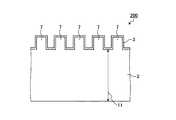
かかる構成を、図1及び2を参照して説明する。図1は、本発明の光学部材の一例を概略的に示す部分断面図であり、図2は本発明の光学部材の別の一例を概略的に示す部分断面図である。図1に示す光学部材100において、凹凸基材6は、矢印10で示す厚さを有する支持層1と、支持層1とは別の部材であり複数の凸部7からなる凹凸構造を有する凹凸構造層5とから構成されている。一方、図2に示す光学部材200において、凹凸基材は、矢印11で示す厚さを有する支持層2のみから構成されており、図1に示す例における凹凸構造5を有しておらず、代わりに支持層2の上面に複数の凸部7からなる凹凸構造が構成されている。 Such a configuration will be described with reference to FIGS. FIG. 1 is a partial sectional view schematically showing an example of the optical member of the present invention, and FIG. 2 is a partial sectional view schematically showing another example of the optical member of the present invention. In the
支持層2のように支持層が凹凸構造を有する場合において、支持層の厚さは、応力分散の効果を有する範囲として、図2の矢印11に示す通り、凸部の高さを含まない厚さとすることができる。ただし、実際の好ましい態様においては、凹凸構造の高さは凹凸基材の厚さに比べて無視できる程度に小さい(図1、図2及び本願のその他の図面において、凹凸構造の図示は概略的なものであり、図示の便宜上、凹凸構造は凹凸基材の厚さに比べて相対的に大きく図示している)。 In the case where the support layer has a concavo-convex structure like the
凹凸基材が、図1に示すように凹凸構造層と支持層とを含む複数の層からなる態様は、下記の理由により好ましい。
(イ)凹凸構造を、支持層より硬度の高いものとすることができ、そのため凹凸構造が強固でありながら応力分散ができる凹凸基材とすることができ、その結果耐擦傷性がさらに向上する。
(ロ)凹凸構造層を薄いものとすることができ、そのため凹凸構造層を、エネルギー線硬化性樹脂、熱硬化性樹脂等の樹脂を材料として用い、支持層上に短時間の工程で形成することができ、その結果、インラインでの効率的な生産が可能となり、長尺の光学部材を低コストで得ることができる。The embodiment in which the uneven substrate is composed of a plurality of layers including an uneven structure layer and a support layer as shown in FIG. 1 is preferable for the following reasons.
(A) The concavo-convex structure can be made harder than the support layer, so that the concavo-convex structure can be made into a concavo-convex base material that can disperse stress while the concavo-convex structure is strong. As a result, the scratch resistance is further improved. .
(B) The concavo-convex structure layer can be made thin, and therefore the concavo-convex structure layer is formed on the support layer in a short time using a resin such as an energy ray curable resin or a thermosetting resin as a material. As a result, in-line efficient production becomes possible, and a long optical member can be obtained at low cost.
(1−2.凹凸構造層)
凹凸基材が、図1に示す例のごとく、支持層とは別の部材として凹凸構造層を有する場合、かかる凹凸構造層の材質は、光学部材として機能しうる任意の材質、例えば入射した光の一部を反射又は透過させる材質とすることができる。具体的には、透明樹脂等の有機材料とすることが、光透過性能と加工の容易さの観点から好ましい。(1-2. Uneven structure layer)
When the concavo-convex base material has a concavo-convex structure layer as a member different from the support layer as in the example shown in FIG. 1, the material of the concavo-convex structure layer is any material that can function as an optical member, for example, incident light. It is possible to use a material that reflects or transmits part of the material. Specifically, an organic material such as a transparent resin is preferable from the viewpoint of light transmission performance and ease of processing.
かかる透明樹脂は、凹凸構造を容易に形成できるという観点から、硬化性樹脂を硬化させたものが好ましい。硬化性樹脂としては、熱硬化性のものと、エネルギー線硬化性のものが挙げられる。エネルギー線は、可視光線、紫外線、電子線、X線を含む。 Such a transparent resin is preferably one obtained by curing a curable resin from the viewpoint that an uneven structure can be easily formed. Examples of the curable resin include thermosetting resins and energy beam curable resins. Energy rays include visible light, ultraviolet rays, electron beams, and X-rays.
熱硬化性樹脂の具体例としては、フェノール樹脂、尿素樹脂、ジアリルフタレート樹脂、メラミン樹脂、グアナミン樹脂、不飽和ポリエステル樹脂、ポリウレタン樹脂、エポキシ樹脂、アミノアルキッド樹脂、メラミン−尿素共縮合樹脂、珪素樹脂、及びポリシロキサン樹脂が挙げられる。 Specific examples of the thermosetting resin include phenol resin, urea resin, diallyl phthalate resin, melamine resin, guanamine resin, unsaturated polyester resin, polyurethane resin, epoxy resin, aminoalkyd resin, melamine-urea cocondensation resin, silicon resin. And polysiloxane resins.
エネルギー線硬化性樹脂としては、ラジカル重合性不飽和基及び/又はカチオン重合性基を有する低分子量化合物、又は樹脂等が挙げられる。なお、ラジカル重合性不飽和基及び/又はカチオン重合性基は、1分子中に2以上含んでいてもよい。 Examples of the energy ray curable resin include a low molecular weight compound having a radically polymerizable unsaturated group and / or a cationically polymerizable group, or a resin. In addition, the radically polymerizable unsaturated group and / or the cation polymerizable group may contain two or more in one molecule.
前記ラジカル重合性不飽和基を有する低分子量化合物としては、エチレン、プロピレン等のα−オレフィン;ブタジエン、イソプレン等の共役ジエン化合物;スチレン、α−メチルスチレン、t−ブチルスチレン、ジビニルベンゼン、ビニルナフタレン、4−ビニルピリジン等のラジカル反応性芳香族化合物;アクリル酸、メタクリル酸、フマール酸、マレイン酸、エンド−ビシクロ[2.2.1]−5−ヘプテン−2,8−ジカルボン酸(エンディック酸)、テトラヒドロフタル酸、イタコン酸、シトラコン酸、クロトン酸、イソクロトン酸等の不飽和カルボン酸;アクリル酸クロライド、メタクリル酸クロライド、マレイン酸クロライド等の不飽和カルボン酸のハライド;アクリルアミド、メタクリルアミド、マレイミド等の不飽和カルボン酸のアミド若しくはイミド誘導体;無水マレイン酸、無水エンディック酸、無水シトラコン酸等の不飽和カルボン酸の無水物;マレイン酸モノメチル、マレイン酸ジメチル、メチル(メタ)アクリレート、エチル(メタ)アクリレート、2−ヒドロキシエチル(メタ)アクリレート、2−ヒドロキシプロピル(メタ)アクリレート、ジメチルアミノエチル(メタ)アクリレート、2−エチルヘキシル(メタ)アクリレート、シクロヘキシル(メタ)アクリレート、イソボルニル(メタ)アクリレート、ジシクロペンテニル(メタ)アクリレート、アリル(メタ)アクリレート、フェニル(メタ)アクリレート、ベンジル(メタ)アクリレート、フエノキシエチル(メタ)アクリレート、へキサンジオールジ(メタ)アクリレート、ネオペンチルグリコールジ(メタ)アクリレート、ジエチレングリコールジ(メタ)アクリレート、トリシクロデカンジメチロールジ(メタ)アクリレート、トリメチロールプロパントリ(メタ)アクリレート、プロピオン酸・ジペンタエリスリトールトリ(メタ)アクリレート、プロピオン酸・ジペンタエリスリトールテトラ(メタ)アクリレート、ジペンタエリスリトールへキサ(メタ)アクリレート等の不飽和カルボン酸のエステル誘導体;ビニルトリクロロシラン、ビニルトリメトキシシラン、ビニルトリエトキシシラン、p−スチリルトリメトキシシラン、3−(メタ)アクリロキシプロピルトリメトキシシラン、3−(メタ)アクリロキシトリエトキシシラン等のラジカル反応不飽和基を有するシラン化合物;等が挙げられる。 Examples of the low molecular weight compound having a radical polymerizable unsaturated group include α-olefins such as ethylene and propylene; conjugated diene compounds such as butadiene and isoprene; styrene, α-methylstyrene, t-butylstyrene, divinylbenzene, and vinylnaphthalene. Radical-reactive aromatic compounds such as 4-vinylpyridine; acrylic acid, methacrylic acid, fumaric acid, maleic acid, endo-bicyclo [2.2.1] -5-heptene-2,8-dicarboxylic acid (endic Acid), tetrahydrophthalic acid, itaconic acid, citraconic acid, crotonic acid, isocrotonic acid and other unsaturated carboxylic acids; acrylic acid chloride, methacrylic acid chloride, maleic acid chloride and other unsaturated carboxylic acid halides; acrylamide, methacrylamide, Unsaturated carbo such as maleimide Amide or imide derivatives of acids; anhydrides of unsaturated carboxylic acids such as maleic anhydride, endic anhydride, citraconic anhydride; monomethyl maleate, dimethyl maleate, methyl (meth) acrylate, ethyl (meth) acrylate, 2-hydroxyethyl (meth) acrylate, 2-hydroxypropyl (meth) acrylate, dimethylaminoethyl (meth) acrylate, 2-ethylhexyl (meth) acrylate, cyclohexyl (meth) acrylate, isobornyl (meth) acrylate, dicyclopentenyl ( (Meth) acrylate, allyl (meth) acrylate, phenyl (meth) acrylate, benzyl (meth) acrylate, phenoxyethyl (meth) acrylate, hexanediol di (meth) acrylate, neopen Diglycol di (meth) acrylate, diethylene glycol di (meth) acrylate, tricyclodecane dimethylol di (meth) acrylate, trimethylolpropane tri (meth) acrylate, propionic acid / dipentaerythritol tri (meth) acrylate, propionic acid / Ester derivatives of unsaturated carboxylic acids such as dipentaerythritol tetra (meth) acrylate and dipentaerythritol hexa (meth) acrylate; vinyltrichlorosilane, vinyltrimethoxysilane, vinyltriethoxysilane, p-styryltrimethoxysilane, 3 Silane compounds having a radical reaction unsaturated group such as-(meth) acryloxypropyltrimethoxysilane, 3- (meth) acryloxytriethoxysilane; and the like.
前記カチオン重合性基を有する低分子量化合物としては、ジシクロペンタジエンジオキサイド、(3,4−エポキシシクロヘキシル)メチル−3,4−エポキシシクロヘキサンカルボキシレート、ビス(2,3−エポキシシクロペンチル)エーテル、ビス(3,4−エポキシシクロヘキシルメチル)アジペート、ビス(3,4−エポキシ−6−メチルシクロヘキシルメチル)アジペート、(3,4−エポキシ−6−メチルシクロヘキシル)メチル−3,4−エポキシ−6−メチルシクロヘキサンカルボキシレート、ビス(3,4−エポキシシクロヘキシルメチル)アセタール、エチレングリコールのビス(3,4−エポキシシクロヘキシル)エーテル、エチレングリコールの3,4−エポキシシクロヘキサンカルボン酸ジエステル等の脂環式エポキシ基を含有する化合物;エチレングリコールジグリシジルエーテル、プロピレングリコールジグリシジルエーテル、ポリエチレングリコールジグリシジルエーテル、ポリプロピレングリコールジグリシジルエーテル、1,4−ブタンジオールジグリシジルエーテル、ネオペンチルグリコールジグリシジルエーテル、1,6−ヘキサンジオールジグリシジルエーテル、グリセリンジグリシジルエーテル、ジグリセリンテトラグリシジルエーテル、トリメチロールプロパントリグリシジルエーテル、スピログリコールジグリシジルエーテル等のグリシジル基を含有するエポキシ化合物;3−エチル−3−メトキシメチルオキセタン、3−エチル−3−エトキシメチルオキセタン、3−エチル−3−ブトキシメチルオキセタン、3−エチル−3−アリルオキシメチルオキセタン、3−メチル−3−ヒドロキシメチルオキセタン、3−エチル−3−ヒドロキシメチルオキセタン、3−エチル−3−(2’−ヒドロキシエチル)オキシメチルオキセタン、3−エチル−3−(2’−ヒドロキシ−3’−フェノキシプロピル)オキシメチルオキセタン、3−エチル−3−(2’−ヒドロキシ−3’−ブトキシプロピル)オキシメチルオキセタン、3−エチル−3−[2’−(2”−エトキシエチル)オキシメチル]オキセタン等のオキセタン環を含有する化合物;等が挙げられる。 Examples of the low molecular weight compound having a cationic polymerizable group include dicyclopentadiene dioxide, (3,4-epoxycyclohexyl) methyl-3,4-epoxycyclohexanecarboxylate, bis (2,3-epoxycyclopentyl) ether, bis (3,4-epoxycyclohexylmethyl) adipate, bis (3,4-epoxy-6-methylcyclohexylmethyl) adipate, (3,4-epoxy-6-methylcyclohexyl) methyl-3,4-epoxy-6-methyl Cyclohexane carboxylate, bis (3,4-epoxycyclohexylmethyl) acetal, bis (3,4-epoxycyclohexyl) ether of ethylene glycol, 3,4-epoxycyclohexanecarboxylic acid diester of ethylene glycol, etc. Compounds containing a poxy group; ethylene glycol diglycidyl ether, propylene glycol diglycidyl ether, polyethylene glycol diglycidyl ether, polypropylene glycol diglycidyl ether, 1,4-butanediol diglycidyl ether, neopentyl glycol diglycidyl ether, 1, Epoxy compounds containing a glycidyl group such as 6-hexanediol diglycidyl ether, glycerin diglycidyl ether, diglycerin tetraglycidyl ether, trimethylolpropane triglycidyl ether, spiroglycol diglycidyl ether; 3-ethyl-3-methoxymethyloxetane 3-ethyl-3-ethoxymethyloxetane, 3-ethyl-3-butoxymethyloxetane, 3-ethyl- -Allyloxymethyloxetane, 3-methyl-3-hydroxymethyloxetane, 3-ethyl-3-hydroxymethyloxetane, 3-ethyl-3- (2'-hydroxyethyl) oxymethyloxetane, 3-ethyl-3- ( 2'-hydroxy-3'-phenoxypropyl) oxymethyloxetane, 3-ethyl-3- (2'-hydroxy-3'-butoxypropyl) oxymethyloxetane, 3-ethyl-3- [2 '-(2 " -Ethoxyethyl) oxymethyl] a compound containing an oxetane ring such as oxetane;
前記ラジカル重合性不飽和基又はカチオン重合性基を有する樹脂としては、低分子量のポリエステル樹脂、ポリエーテル樹脂、アクリル樹脂、メタクリル樹脂、エポキシ樹脂、ウレタン樹脂、アルキッド樹脂、スピロアセタール樹脂、ポリブタジエン樹脂、ポリチオールポリエン樹脂等の側鎖にラジカル重合性不飽和基又はカチオン重合性基を有する樹脂が挙げられる。 Examples of the resin having a radical polymerizable unsaturated group or a cationic polymerizable group include low molecular weight polyester resins, polyether resins, acrylic resins, methacrylic resins, epoxy resins, urethane resins, alkyd resins, spiroacetal resins, polybutadiene resins, Examples thereof include resins having a radically polymerizable unsaturated group or a cationically polymerizable group in the side chain such as a polythiol polyene resin.
エネルギー線として紫外線や可視光線を用いる場合には、硬化性樹脂の中に光重合開始剤、光増感剤などを含ませることができる。光重合開始剤としては、アセトフェノン類、ベンゾフェノン類、ミヒラーベンゾイルベンゾエート、α−アミロキシムエステル、テトラメチルチウラムモノサルファイド、チオキサントン類等が挙げられる。光増感剤としてn−ブチルアミン、トリエチルアミン、トリ−n−ブチルホスフィン等が挙げられる。 When ultraviolet rays or visible rays are used as energy rays, a photopolymerization initiator, a photosensitizer, or the like can be included in the curable resin. Examples of the photopolymerization initiator include acetophenones, benzophenones, Michler benzoylbenzoate, α-amyloxime ester, tetramethylthiuram monosulfide, thioxanthones, and the like. Examples of the photosensitizer include n-butylamine, triethylamine, and tri-n-butylphosphine.
凹凸基材を構成する透明樹脂は、加工性の観点からガラス転移温度が60〜200℃であることが好ましく、100〜180℃であることがより好ましい。なお、ガラス転移温度は示差走査熱量分析(DSC)により測定することができる。 The transparent resin constituting the concavo-convex base material preferably has a glass transition temperature of 60 to 200 ° C., more preferably 100 to 180 ° C. from the viewpoint of processability. The glass transition temperature can be measured by differential scanning calorimetry (DSC).
前記透明樹脂は、顔料や染料のごとき着色剤、蛍光増白剤、分散剤、熱安定剤、光安定剤、紫外線吸収剤、帯電防止剤、酸化防止剤、滑剤、溶剤などの配合剤が適宜配合されたものであってもよい。 The transparent resin may be appropriately mixed with coloring agents such as pigments and dyes, fluorescent brighteners, dispersants, heat stabilizers, light stabilizers, UV absorbers, antistatic agents, antioxidants, lubricants, solvents, and the like. It may be blended.
前記透明樹脂は、100℃で2時間真空乾燥した後の重量W0から、80℃の温水に24時間浸漬し次いで100℃で2時間真空乾燥した後の重量W1への重量減量が、W0の1%以下であることが好ましく、0.8%以下であることがより好ましい。 The weight loss of the transparent resin from weight W0 after vacuum drying at 100 ° C. for 2 hours to weight W1 after immersion in warm water at 80 ° C. for 24 hours and then vacuum drying at 100 ° C. for 2 hours is 1 of W0. % Or less, and more preferably 0.8% or less.
本発明において、凹凸基材は、上に説明した支持層を構成する樹脂及び任意に凹凸構造層を構成する樹脂のみから構成することもできるが、樹脂に加えて他の材料を組み合わせて構成することもできる。例えば、後に詳述するグリッド偏光子のように、透明樹脂の層に加えて金属層を有し、これらの組み合わせにより構成されていてもよい。 In the present invention, the concavo-convex substrate can be composed of only the resin constituting the support layer described above and optionally the resin constituting the concavo-convex structure layer, but is composed by combining other materials in addition to the resin. You can also. For example, like a grid polarizer described in detail later, a metal layer may be provided in addition to a transparent resin layer, and a combination thereof may be used.
凹凸基材が凹凸構造層を有する場合の凹凸構造層の厚さ(図1の矢印12で示される)は、200nm〜20μmであることが好ましい。上記下限以上とすることにより、欠陥のない凹凸構造を安定して製造することができ、また上記上限以下とすることにより、使用に際し凹凸構造にかかる応力を良好に分散することができ、コスト及び部材の重量を低減することができる。 When the concavo-convex substrate has the concavo-convex structure layer, the thickness of the concavo-convex structure layer (indicated by the
(1−3.凹凸構造)
本発明において、凹凸基材は、凹凸構造を有する凹凸面を、その表面の少なくとも一部に有する。凹凸面は、図2の例に示されるように支持層の面上に設けることもでき、図1の例に示されるように支持層以外の層である凹凸構造層の面上に設けることもできる。(1-3. Uneven structure)
In the present invention, the concavo-convex substrate has a concavo-convex surface having a concavo-convex structure on at least a part of its surface. The uneven surface can be provided on the surface of the support layer as shown in the example of FIG. 2, or can be provided on the surface of the uneven structure layer which is a layer other than the support layer as shown in the example of FIG. it can.
凹凸構造は、周期が900nm以下の凹凸構造とすることができる。ここで、凹凸構造の周期とは、凹凸面上の一方向に沿って観察した際に、複数の同一形状の凹凸が繰り返し現れる場合における、一つの凹凸の幅(即ち当該一方向に沿った長さ)ということを意味することができる。
凹凸面上の複数方向において凹凸構造の周期が存在する場合は、それらのうち最も短いものを周期とすることができる。以下においては、特に断らない限り、最も短い周期を単に周期という。The uneven structure can be an uneven structure with a period of 900 nm or less. Here, the period of the concavo-convex structure is the width of one concavo-convex (that is, the length along the one direction) when a plurality of concavo-convex parts having the same shape appear repeatedly when observed along one direction on the concavo-convex surface. Can mean).
When the period of the concavo-convex structure exists in a plurality of directions on the concavo-convex surface, the shortest of them can be used as the period. In the following, unless otherwise specified, the shortest cycle is simply called a cycle.
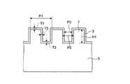
これを図3及び図4に示す例を参照して説明する。図3は、図1に示す光学部材の一例の凹凸構造を拡大して示す部分断面図であり、図4は、図1に示す光学部材の一例における凹凸基材を概略的に示す斜視図である。図4において、凹凸基材6は、座標軸X及びYに平行な面方向に延長するフィルムであり、その上面の全面が、座標軸Yに平行に延長した多数の畝状の凸部7からなる凹凸構造を有する凹凸面である。断面図である図3の断面は、図4に示す座標軸X及びZに平行な面における断面である。この例において、凹凸構造7は、図4のY軸方向に延長する畝状の構造であるため、凹凸構造の最も短い周期は、座標軸X方向、即ち図3における図面の左右方向における周期となる。したがって、凸部7が繰り返し現れる凹凸構造における周期は、図3の矢印P1で示される距離となる。
凹凸構造の周期のより好ましい長さは、作製する光学部材の性能により変動するため特に限定されないが、より好ましくは20〜800nmとすることができる。This will be described with reference to the examples shown in FIGS. 3 is an enlarged partial cross-sectional view showing an example of the uneven structure of the optical member shown in FIG. 1, and FIG. 4 is a perspective view schematically showing the uneven substrate in the example of the optical member shown in FIG. is there. In FIG. 4, the concavo-
Although the more preferable length of the period of the concavo-convex structure varies depending on the performance of the optical member to be manufactured, it is not particularly limited, but more preferably 20 to 800 nm.
本発明において、凹凸構造の具体的な形状は、光学的な特性を発揮しうる様々な微細な構造とすることができるが、表面に多数の突起を有するモスアイ構造、構造複屈折波長板又は以下に詳述するグリッド偏光子として機能しうる畝状の凹凸構造を例示することができる。 In the present invention, the specific shape of the concavo-convex structure can be various fine structures capable of exhibiting optical characteristics, but a moth-eye structure having a large number of protrusions on the surface, a structural birefringent wave plate or the following An eaves-like concavo-convex structure that can function as a grid polarizer described in detail in FIG.
(1−4.畝状の凹凸構造)
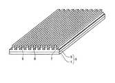
前記畝状の凹凸構造は、図3〜4の例に示すもののように、凹凸基材の少なくとも一方の表面に略平行に並ぶ複数の畝を有するものである。畝の周期は、可視光線の波長よりも短いことが好ましい。該畝は、稜線が略直線状に延びるものである。畝の垂直断面形状は特に限定されないが、矩形、台形、菱形、山形などが挙げられる。(1-4. Bowl-shaped uneven structure)
The ridge-like concavo-convex structure has a plurality of ridges arranged substantially parallel to at least one surface of the concavo-convex base material, as shown in the examples of FIGS. The wrinkle cycle is preferably shorter than the wavelength of visible light. The ridge has a ridge line extending substantially linearly. The vertical cross-sectional shape of the ridge is not particularly limited, and examples thereof include a rectangle, a trapezoid, a diamond, and a mountain.
畝の高さ(図3において矢印H1で示される)は、好ましくは5〜3000nm、より好ましくは20〜1000nm、特に好ましくは50〜300nmである。
畝間に形成される溝の幅は、好ましくは200nm以下、好ましくは20〜100nmである。
畝の幅は、好ましくは25〜300nmであり、畝(稜線)の長さは、好ましくは800nm以上である。
また、畝の中心間距離(ピッチ)即ち畝の周期P1は、好ましくは20〜500nm、より好ましくは30〜300nmである。
畝のアスペクト比(畝の高さ/畝の幅)は、好ましくは0.1〜5.0、より好ましくは0.4〜3.0、特に好ましくは0.8〜2.0である。The height of the ridge (indicated by arrow H1 in FIG. 3) is preferably 5 to 3000 nm, more preferably 20 to 1000 nm, and particularly preferably 50 to 300 nm.
The width of the groove formed between the ribs is preferably 200 nm or less, preferably 20 to 100 nm.
The width of the ridge is preferably 25 to 300 nm, and the length of the ridge (ridge line) is preferably 800 nm or more.
Moreover, the distance (pitch) between the centers of the wrinkles, that is, the period P1 of the wrinkles is preferably 20 to 500 nm, more preferably 30 to 300 nm.
The aspect ratio of the ridge (the height of the ridge / the width of the ridge) is preferably 0.1 to 5.0, more preferably 0.4 to 3.0, and particularly preferably 0.8 to 2.0.
偏光分離性能などの光学特性を考慮すると、畝が略平行に周期的に(同一ピッチで)並んだものが好ましい。なお、本発明において、略平行とは、平行方向から±5°の範囲内にあることをいう。 In consideration of optical characteristics such as polarization separation performance, it is preferable that the ridges are arranged approximately in parallel and periodically (at the same pitch). In the present invention, “substantially parallel” means within a range of ± 5 ° from the parallel direction.
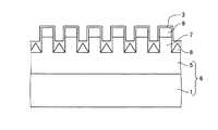
本発明において、畝状の凹凸構造は、上に述べた透明樹脂に加えて、畝の頂に在る金属層A及び/又は前記畝間に形成される溝の底に在る金属層Bによって構成することができる。 In the present invention, the ridge-like uneven structure is constituted by the metal layer A at the top of the ridge and / or the metal layer B at the bottom of the groove formed between the ridges in addition to the transparent resin described above. can do.
金属層(グリッド線)に用いる材料としては、導電性のものが好ましく、具体的には、アルミニウム、インジウム、マグネシウム、ロジウム、スズ等の金属が挙げられる。
金属層は、前記材料を物理蒸着(PVD法)することによって形成することができる。
PVD法は、蒸着材料を蒸発・イオン化し、被膜を形成させる方法である。具体的には、真空蒸着法、スパッタリング法、イオンプレーティング(イオンめっき)法、イオンビームデポジション法等が挙げられる。これらのうち表面粗さを小さくすることが容易という観点から真空蒸着法が好ましい。真空蒸着法は、真空にした容器の中で、蒸着材料を加熱し気化もしくは昇華して、離れた位置に置かれた基材の表面に付着させ、薄膜を形成する方法である。加熱手段としては、抵抗加熱、電子ビーム、高周波誘導、レーザーなどが挙げられる。物理蒸着を行う装置内の雰囲気は、好ましくは絶対圧1×10⁻²Pa以下、より好ましくは絶対圧8×10⁻³Pa以下である。
物理蒸着による製膜速度は、好ましくは1.0nm/秒以上、より好ましくは2.5nm/秒以上、特に好ましくは4.0nm/秒以上である。なお、製膜速度の上限は、製膜装置の性能による限界があるのみで、表面粗さを小さくするという観点においては特に制限されない。製膜速度をこの範囲に調整することによって、表面粗さを小さくすることができる。The material used for the metal layer (grid line) is preferably a conductive material, and specific examples include metals such as aluminum, indium, magnesium, rhodium, and tin.
The metal layer can be formed by physical vapor deposition (PVD method) of the material.
The PVD method is a method of forming a film by evaporating and ionizing a vapor deposition material. Specific examples include vacuum deposition, sputtering, ion plating (ion plating), and ion beam deposition. Of these, vacuum vapor deposition is preferred from the viewpoint of easy surface roughness reduction. The vacuum deposition method is a method of forming a thin film by heating and vaporizing or sublimating a deposition material in a vacuumed container and attaching it to the surface of a substrate placed at a remote position. Examples of the heating means include resistance heating, electron beam, high frequency induction, and laser. The atmosphere in the apparatus for performing physical vapor deposition is preferably an absolute pressure of 1 × 10⁻² Pa or less, more preferably an absolute pressure of 8 × 10⁻³ Pa or less.
The film formation rate by physical vapor deposition is preferably 1.0 nm / second or more, more preferably 2.5 nm / second or more, and particularly preferably 4.0 nm / second or more. Note that the upper limit of the film forming speed is limited only by the performance of the film forming apparatus, and is not particularly limited from the viewpoint of reducing the surface roughness. By adjusting the film forming speed within this range, the surface roughness can be reduced.
畝を有する透明樹脂基材にPVD法により金属層を形成させた場合、前記畝の頂および/または前記畝間に形成される溝の底に金属層が積層される。 When a metal layer is formed on the transparent resin substrate having ridges by the PVD method, the metal layer is laminated on the top of the ridge and / or the bottom of the groove formed between the ridges.
畝の頂に積層された金属層Aの形状は特に制限されず、通常は矩形、台形、円形、山形などである。金属層Aの厚さは、特に制限されないが、好ましくは100nm以下、より好ましくは30〜90nm、特に好ましくは50〜80nmである。金属層Aの幅および長さは、通常、畝の頂面の形状にしたがってほぼ決まる。 The shape of the metal layer A laminated on the top of the ridge is not particularly limited, and is usually rectangular, trapezoidal, circular, mountain-shaped, or the like. The thickness of the metal layer A is not particularly limited, but is preferably 100 nm or less, more preferably 30 to 90 nm, and particularly preferably 50 to 80 nm. The width and length of the metal layer A are generally determined according to the shape of the top surface of the ridge.
畝間に形成される溝の底に積層された金属層Bの形状は、特に制限されず、通常は矩形、台形、円形、山形などである。金属層Bの厚さは、好ましくは100nm以下、より好ましくは30〜90nm、特に好ましくは50〜80nmである。金属層Bの幅および長さは、通常、溝の底面の形状にしたがってほぼ決まる。 The shape of the metal layer B laminated on the bottom of the groove formed between the ribs is not particularly limited, and is usually rectangular, trapezoidal, circular, mountain-shaped, or the like. The thickness of the metal layer B is preferably 100 nm or less, more preferably 30 to 90 nm, and particularly preferably 50 to 80 nm. The width and length of the metal layer B are generally determined according to the shape of the bottom surface of the groove.
また、必要に応じて、望ましい金属層の形状を形成するために、金属層の形成前に、無機誘電体で透明性がある材料をスパッタリングして、その後に金属層を形成する方法がある。ここで、無機誘電体で透明性がある材料としては、二酸化ケイ素、二酸化チタン、酸化アルミニウム等を使用することができる。 Further, if necessary, there is a method of forming a metal layer by sputtering an inorganic dielectric material having transparency before forming the metal layer in order to form a desired metal layer shape. Here, silicon dioxide, titanium dioxide, aluminum oxide, or the like can be used as the inorganic dielectric material having transparency.
図5及び図6は、本発明における、透明樹脂層及び金属層を有する凹凸基材の一例を示す斜視図及び断面図である。図5及び図6において、支持層1及び凹凸構造層5からなる凹凸基材6の構造は、図3及び図4に示すものと同様である。図5及び図6の例に示すように、凹凸構造層5の上面の矩形畝状の凸部7からなる凹凸構造の頂部及び畝間部の両方に、それぞれ断面概略矩形及び三角形の金属層8及び9が積層された構造とすることができる。かかる金属層9のような断面形状の金属層は、断面矩形に形成した金属層を、以下に詳述するエッチング等の手段により変形させることにより得ることができる。 5 and 6 are a perspective view and a cross-sectional view showing an example of an uneven substrate having a transparent resin layer and a metal layer in the present invention. 5 and 6, the structure of the concavo-
前記のような畝形成面に積層された金属層の一部は、湿式エッチングによって除去することが好ましい。除去される金属層の一部とは、畝の側壁に形成された部分、畝の頂の幅からはみ出した部分などである。湿式エッチングは、金属層にエッチング液を接触させる工程と、リンス液で洗浄する工程、およびリンス液を除去する工程を少なくとも含む。 It is preferable to remove a part of the metal layer laminated on the ridge forming surface as described above by wet etching. The part of the metal layer to be removed includes a part formed on the side wall of the ridge, a part protruding from the width of the top of the ridge, and the like. The wet etching includes at least a step of bringing an etching solution into contact with the metal layer, a step of washing with a rinse solution, and a step of removing the rinse solution.
金属層にエッチング液を接触させる工程の前に、除去されないようにしたい部分の金属層の上にマスク層を設けてもよい。マスク層には、通常、無機化合物膜が用いられる。このマスク層によって金属層の厚さの減少を少なくして金属層の幅を狭くすることができる。 Before the step of bringing the etching solution into contact with the metal layer, a mask layer may be provided on a portion of the metal layer that is desired not to be removed. In general, an inorganic compound film is used for the mask layer. The mask layer can reduce the thickness of the metal layer by reducing the decrease in the thickness of the metal layer.
マスキング用の無機化合物は、後述の湿式エッチングに耐えるものであれば特に限定されず、例えば、二酸化ケイ素、窒化ケイ素、炭化ケイ素または窒化酸化ケイ素などの化合物が挙げられる。これらの中では特に二酸化ケイ素が好ましい。積層される無機化合物膜の厚さは、特に制限されないが、通常1〜100nm、好ましくは2〜50nm、より好ましくは3〜20nmである。無機化合物膜はPVD法によって形成できる。 The inorganic compound for masking is not particularly limited as long as it can withstand wet etching described later, and examples thereof include compounds such as silicon dioxide, silicon nitride, silicon carbide, and silicon nitride oxide. Of these, silicon dioxide is particularly preferred. The thickness of the laminated inorganic compound film is not particularly limited, but is usually 1 to 100 nm, preferably 2 to 50 nm, and more preferably 3 to 20 nm. The inorganic compound film can be formed by a PVD method.
金属層にエッチング液を接触させる工程の前に、略平行に並んだ畝に直交する方向に延伸することができる。この延伸によって畝の中心間距離が広がり、金属層A間のピッチ間隔が広がり、結果として光線透過率が高くなる。また溝の底面に形成されていた金属層Bの端が、延伸によって、畝の基部から離れ、隙間ができる。後述する湿式エッチング液がこの隙間に入り込み、金属層Bの両端を優先的に除去し、図3のように、金属層Bの断面における中央部分よりも両端部分を薄くし、概略三角形の断面形状とすることができる。 Before the step of bringing the etching solution into contact with the metal layer, the metal layer can be stretched in a direction perpendicular to the ridges arranged in parallel. By this stretching, the distance between the centers of the ridges is increased, the pitch interval between the metal layers A is increased, and as a result, the light transmittance is increased. Moreover, the end of the metal layer B formed on the bottom surface of the groove is separated from the base portion of the ridge by stretching, and a gap is formed. A wet etching solution, which will be described later, enters this gap and removes both ends of the metal layer B preferentially, and as shown in FIG. It can be.
延伸方法は特に限定されないが、畝に直交する方向の延伸倍率を好ましくは1.05〜5倍、より好ましくは1.1〜3倍、畝に平行な方向の延伸倍率を好ましくは0.9〜1.1倍、より好ましくは0.95〜1.05倍にするとよい。このような延伸を行うために、テンター延伸機による連続的な横一軸延伸が好適である。 The stretching method is not particularly limited, but the stretching ratio in the direction perpendicular to the ridge is preferably 1.05 to 5 times, more preferably 1.1 to 3 times, and the stretching ratio in the direction parallel to the ridge is preferably 0.9. It is good to make it -1.1 times, more preferably 0.95-1.05 times. In order to perform such stretching, continuous transverse uniaxial stretching by a tenter stretching machine is suitable.
金属層にエッチング液を接触させる工程の前に、金属層の表面改質処理を行うことが好ましい。表面改質処理としては、プラズマ処理、コロナ放電処理、UV照射処理および有機溶剤処理からなる群から選ばれる少なくとも一つの処理が好適なものとして挙げられる。金属層の表面改質処理を行うことによって、光学性能のバラツキが小さくなる。 Before the step of bringing the etching solution into contact with the metal layer, it is preferable to perform a surface modification treatment of the metal layer. Suitable examples of the surface modification treatment include at least one treatment selected from the group consisting of plasma treatment, corona discharge treatment, UV irradiation treatment, and organic solvent treatment. By performing the surface modification treatment of the metal layer, variation in optical performance is reduced.
湿式エッチングに用いられるエッチング液は、透明樹脂フィルムを腐食等させずに金属層の一部を除去できる液であれば良く、マスク層(無機化合物膜)、金属層、透明樹脂基材の材質に応じて適宜選択される。エッチング液としては、水酸化ナトリウム、水酸化カリウム等のアルカリ金属化合物を含有する溶液;硫酸、燐酸、硝酸、酢酸、フッ化水素、塩酸などを含有する溶液;過硫酸アンモニウム、過酸化水素、フッ化アンモニウム等やそれらの混合液からなる溶液などが挙げられる。また、エッチング液には界面活性剤などの添加剤が含まれていても良い。 The etching solution used for the wet etching may be a solution that can remove a part of the metal layer without corroding the transparent resin film, and can be used as a material for the mask layer (inorganic compound film), the metal layer, and the transparent resin substrate. It is selected as appropriate. Etching solutions include solutions containing alkali metal compounds such as sodium hydroxide and potassium hydroxide; solutions containing sulfuric acid, phosphoric acid, nitric acid, acetic acid, hydrogen fluoride, hydrochloric acid, etc .; ammonium persulfate, hydrogen peroxide, fluoride Examples include ammonium and the like, and solutions made of a mixture thereof. The etching solution may contain an additive such as a surfactant.
金属層にエッチング液を接触させる方法は、特に制限されないが、ディップ法、スプレー法およびコーティング法からなる群から選ばれる少なくとも一つの方法が好ましい。 A method for bringing the etching solution into contact with the metal layer is not particularly limited, but at least one method selected from the group consisting of a dipping method, a spray method, and a coating method is preferable.
湿式エッチングに用いられるリンス液は、エッチング液を金属層に接触させたときに発生した残渣を取り除く液である。残渣が残ると金属層の表面が荒れ、光学性能に影響を及ぼすことがある。また、残渣が透明樹脂基材の好ましく無い場所に付着することがある。
リンス液としては、水(例えば、純水など)、界面活性剤を含有する溶液、などが挙げられる。
リンス液で金属層を洗浄する方法は、金属層に接触したエッチング液およびエッチング残渣を取り除くことができる方法であれば、特に制限されない。The rinsing liquid used for the wet etching is a liquid that removes residues generated when the etching liquid is brought into contact with the metal layer. If the residue remains, the surface of the metal layer becomes rough, which may affect the optical performance. Moreover, a residue may adhere to the unpreferable location of a transparent resin base material.
Examples of the rinse liquid include water (for example, pure water), a solution containing a surfactant, and the like.
The method of cleaning the metal layer with the rinsing liquid is not particularly limited as long as it is a method that can remove the etching liquid and the etching residue that are in contact with the metal layer.
リンス液で洗浄した後、リンス液を除去する。リンス液の除去方法は特に制限されないが、エアーブローによる方法が好ましい。 After washing with the rinse solution, the rinse solution is removed. The method for removing the rinsing liquid is not particularly limited, but an air blow method is preferred.
凹凸基材における金属層には、腐食防止処理を施して腐食防止膜を設けても良い。腐食防止膜は、グリッド偏光性能の観点から、単分子膜もしくはそれに準じる厚さ、具体的には、100nm以下、好ましくは50nm以下の厚さであることが好ましい。 The metal layer in the concavo-convex substrate may be provided with a corrosion prevention film by performing a corrosion prevention treatment. From the viewpoint of grid polarization performance, the corrosion prevention film is preferably a monomolecular film or a thickness equivalent thereto, specifically, a thickness of 100 nm or less, preferably 50 nm or less.
(1−5.凹凸基材の形状)
凹凸基材の形状は、その表面の少なくとも一部において前記凹凸面を有する限りにおいて特に限定されないが、通常フィルム又は板状の形状とすることができ、当該フィルム又板の表裏の主面のうちの片面又は両面の少なくとも一部において、前記凹凸構造を有する凹凸面が設けられることが好ましい。(1-5. Shape of uneven substrate)
The shape of the concavo-convex substrate is not particularly limited as long as it has the concavo-convex surface in at least a part of the surface thereof, but can be usually a film or a plate-like shape, among the main surfaces of the front and back of the film or plate It is preferable that a concavo-convex surface having the concavo-convex structure is provided on at least a part of one side or both sides.
凹凸基材がフィルムの形状である場合における平均厚さは、取り扱い性の観点から通常5μm〜10mm、好ましくは20〜500μmである。凹凸基材は、波長400〜700nmの可視光線領域の光の透過率が80%以上であるものが好ましい。 The average thickness when the concavo-convex base material is in the form of a film is usually 5 μm to 10 mm, preferably 20 to 500 μm from the viewpoint of handleability. The uneven substrate preferably has a light transmittance of 80% or more in the visible light region having a wavelength of 400 to 700 nm.
本発明に用いられる光学部材を製造するにあたって、凹凸基材として長尺状のものが好ましく用いられる。長尺とは、幅に対し少なくとも5倍程度以上の長さを有するものを言い、好ましくは10倍もしくはそれ以上の長さを有するものを言い、具体的にはロール状に巻回されて保管または運搬される程度の長さを有するものを言う。 In manufacturing the optical member used in the present invention, an elongated base material is preferably used. “Long” means a material having a length of at least about 5 times the width, preferably a material having a length of 10 times or more, and specifically wound and stored in a roll shape. Or what has the length of the grade carried.
長尺状の凹凸基材の幅は、好ましくは500mm以上、より好ましくは1000mm以上である。凹凸基材は、その製造工程の途中において、任意に、その幅方向の両端を切り落とす(トリミング)ことがある。この場合、前記凹凸基材の幅は、両端を切り落とした後の寸法とすることができる。 The width of the long uneven substrate is preferably 500 mm or more, more preferably 1000 mm or more. In the course of the manufacturing process, the concavo-convex base material may be arbitrarily cut off (trimming) at both ends in the width direction. In this case, the width of the concavo-convex base material can be a dimension after cutting off both ends.
2.保護層
本発明の光学部材は、前記凹凸基材の凹凸面上に設けられた保護層を有する。
保護層は、凹凸基材の凹凸面の少なくとも一部の上に設けることができるが、好ましくは凹凸面全面の上に設け、凹凸面を保護することができる。
(2−1.保護層の材料)2. Protective layer The optical member of the present invention has a protective layer provided on the uneven surface of the uneven substrate.
The protective layer can be provided on at least a part of the concavo-convex surface of the concavo-convex base material, but is preferably provided on the entire concavo-convex surface to protect the concavo-convex surface.
(2-1. Material of protective layer)
保護層を構成する材料は、有機材料を含むことが好ましい。
前記有機材料は、透明樹脂であることが好ましい。透明樹脂は、前述の透明樹脂基材を構成するものとして示した、熱硬化性樹脂、エネルギー線硬化性樹脂、およびこれらの混合物を用いることができる。なお、エネルギー線とは、可視光線、紫外線、電子線、などのことをいう。
熱硬化性樹脂としては、フェノール樹脂、尿素樹脂、ジアリルフタレート樹脂、メラミン樹脂、グアナミン樹脂、不飽和ポリエステル樹脂、ポリウレタン樹脂、エポキシ樹脂、アミノアルキッド樹脂、メラミン−尿素共縮合樹脂、珪素樹脂、ポリシロキサン樹脂等が使用でき、これらの樹脂には必要に応じて、架橋剤、重合開始剤等の硬化剤、重合促進剤、溶剤、粘度調整剤等を加えることができる。
エネルギー線硬化型樹脂としては、製造が容易である点から、アクリレート系の官能基を有するものが好ましい。例えば、比較的低分子量のポリエステル樹脂、ポリエーテル樹脂、アクリル樹脂、エポキシ樹脂、ウレタン樹脂、アルキッド樹脂、スピロアセタール樹脂、ポリブタジエン樹脂、ポリチオールポリエン樹脂、多価アルコール等の多官能化合物の(メタ)アクリレート等のオリゴマーまたはプレポリマーおよび反応性希釈剤としてエチル(メタ)アクリレート、エチルヘキシル(メタ)アクリレート、スチレン、メチルスチレン、N−ビニルピロリドン等の単官能モノマー並びに多官能モノマー、例えば、トリメチロールプロパントリ(メタ)アクリレート、ヘキサンジオール(メタ)アクリレート、トリプロピレングリコールジ(メタ)アクリレート、ジエチレングリコールジ(メタ)アクリレート、ペンタエリスリトールトリ(メタ)アクリレート、ジペンタエリスリトールヘキサ(メタ)アクリレート、1、6−ヘキサンジオールジ(メタ)アクリレート、ネオペンチルグリコールジ(メタ)アクリレート等を比較的多量に含有するものが使用できる。エネルギー線として紫外線や可視光線を用いる場合には、この中に光重合開始剤として、アセトフェノン類、ベンゾフェノン類、ミヒラーベンゾイルベンゾエート、α−アミロキシムエステル、テトラメチルチウラムモノサルファイド、チオキサントン類や、光増感剤としてn−ブチルアミン、トリエチルアミン、トリ−n−ブチルホスフィン等を混合して用いることができる。The material constituting the protective layer preferably contains an organic material.
The organic material is preferably a transparent resin. As the transparent resin, a thermosetting resin, an energy ray curable resin, and a mixture thereof, which are shown as constituting the above-described transparent resin base material, can be used. In addition, an energy ray means visible light, an ultraviolet-ray, an electron beam, etc.
Thermosetting resins include phenolic resin, urea resin, diallyl phthalate resin, melamine resin, guanamine resin, unsaturated polyester resin, polyurethane resin, epoxy resin, aminoalkyd resin, melamine-urea co-condensation resin, silicon resin, polysiloxane Resins and the like can be used, and a curing agent such as a crosslinking agent and a polymerization initiator, a polymerization accelerator, a solvent, a viscosity modifier and the like can be added to these resins as necessary.
As the energy ray curable resin, those having an acrylate functional group are preferable from the viewpoint of easy production. For example, relatively low molecular weight polyester resins, polyether resins, acrylic resins, epoxy resins, urethane resins, alkyd resins, spiroacetal resins, polybutadiene resins, polythiol polyene resins, (meth) acrylates of polyfunctional compounds such as polyhydric alcohols Monofunctional monomers such as oligomers or prepolymers such as ethyl (meth) acrylate, ethylhexyl (meth) acrylate, styrene, methylstyrene, N-vinylpyrrolidone as reactive diluents and polyfunctional monomers such as trimethylolpropane tri ( (Meth) acrylate, hexanediol (meth) acrylate, tripropylene glycol di (meth) acrylate, diethylene glycol di (meth) acrylate, pentaerythritol tri (meth) acrylate Rate, dipentaerythritol hexa (meth) acrylate, 1,6-hexanediol di (meth) acrylate, those of relatively high content of neopentyl glycol di (meth) acrylate can be used. When ultraviolet rays or visible rays are used as energy rays, acetophenones, benzophenones, Michler benzoylbenzoate, α-amyloxime ester, tetramethylthiuram monosulfide, thioxanthones, and photopolymerization initiators are used. As a sensitizer, n-butylamine, triethylamine, tri-n-butylphosphine and the like can be mixed and used.
保護層を構成する有機材料は、前述の透明樹脂基材同様に、前記同様の方法で測定した重量減量が1%以下であることが好ましく、0.8%以下であることがより好ましい。 As for the organic material constituting the protective layer, the weight loss measured by the same method as described above is preferably 1% or less, and more preferably 0.8% or less, like the transparent resin substrate described above.
保護層を構成する有機材料は、厚さ10μmでの鉛筆硬度がF以上であることが好ましく、2H以上であることがより好ましい。ここでいう鉛筆硬度は、有機材料を厚さ10μmで、保護層の形成と同様の条件で硬化させた際の硬度である。鉛筆硬度はJIS K5600に準じ測定することができる。 The organic material constituting the protective layer preferably has a pencil hardness of F or more at a thickness of 10 μm, more preferably 2H or more. The pencil hardness here is the hardness when the organic material is cured at a thickness of 10 μm under the same conditions as those for forming the protective layer. The pencil hardness can be measured according to JIS K5600.
(2−2.保護層の特性)
凹凸基材の凹凸面上に形成した保護層は、図1〜図3及び図5の例においては符号3で示される。拡大断面図である図3を参照して説明すると、保護層3の厚さは凹凸構造の凸部間の空隙の幅P2の半分より十分に薄くすることが好ましく、その結果、保護層間の空隙の幅P3を有した凹凸構造が、保護層3の面上に形成することができる。このように、保護層により凹凸構造を埋めることなく、保護層が凹凸構造に追従した形状とすることにより、凹凸構造の光学的性能を損ねることなく、凹凸構造を効果的に保護することが可能となる。(2-2. Characteristics of protective layer)
The protective layer formed on the concavo-convex surface of the concavo-convex substrate is denoted by
本発明の光学部材においては、保護層の厚さと前記支持層の厚さとの相対的な関係が、下記の要件を満たす。即ち、(支持層の厚さ)/(保護層の厚さ)の比が1000以上、好ましくは3000以上である。かかる厚さの比率を有することにより、応力を良好に分散することができる。(支持層の厚さ)/(保護層の厚さ)の比の上限は、制限はないが、光学的特性、光学部材として使用した際の現実的な観点から20000以下、好ましくは10000以下である。ここで、保護層の厚さは、凹凸構造の凸部上における保護層の平均厚さとする。 In the optical member of the present invention, the relative relationship between the thickness of the protective layer and the thickness of the support layer satisfies the following requirements. That is, the ratio of (support layer thickness) / (protective layer thickness) is 1000 or more, and preferably 3000 or more. By having such a thickness ratio, the stress can be well dispersed. The upper limit of the ratio of (thickness of the support layer) / (thickness of the protective layer) is not limited, but is 20000 or less, preferably 10,000 or less from the practical viewpoint when used as an optical member and optical characteristics. is there. Here, the thickness of the protective layer is the average thickness of the protective layer on the convex portion of the concavo-convex structure.
保護層の平均厚さは、凹凸構造の光学的性能を損ねることなく凹凸構造を保護するため、50nm以下であることが好ましく、さらに好ましくは2〜40nmである。保護層の厚さは、光学部材をウルトラミクロトーム等を用いて切断し、その断面を透過型電子顕微鏡等を用いて観察することにより測定できる。かかる50nm以下の厚さとすると、保護層を構成する重合性単量体等の分子が厚さ方向に1分子のみ又は2分子以上重なる状態の層とすることができ、薄い膜厚でありながら良好な強度を有した保護層とするのに特に好適である。 The average thickness of the protective layer is preferably 50 nm or less, and more preferably 2 to 40 nm in order to protect the uneven structure without impairing the optical performance of the uneven structure. The thickness of the protective layer can be measured by cutting the optical member with an ultramicrotome or the like and observing the cross section with a transmission electron microscope or the like. When the thickness is 50 nm or less, a layer in which only one molecule or two or more molecules such as a polymerizable monomer constituting the protective layer overlap in the thickness direction can be formed, and the film is thin but good It is particularly suitable for a protective layer having a high strength.
保護層は、凹凸構造の頂部に少なくとも存在すれば良く、谷部および側面部において保護層が均一である必要はない。ただし、側面部の厚さT2とすると、T2×2<P2かつ、谷部の厚さT3とすると、T3<Hであることが光学特性の観点から好ましい。
ここでいう保護層の平均厚さとは、凸部上の保護層の厚みの平均の厚さを示す。The protective layer only needs to exist at least on the top of the concavo-convex structure, and the protective layer does not need to be uniform in the valley portion and the side surface portion. However, when T2 × 2 <P2 is set for the thickness T2 of the side surface and T3 <H is preferable for the thickness T3 of the valley, from the viewpoint of optical characteristics.
The average thickness of the protective layer here refers to the average thickness of the protective layer on the convex portion.
保護層は、波長400〜700nmの可視光線領域の光の透過率が80%以上であるものが好ましい。
また、保護層は、本発明の効果を阻害しない範囲で顔料や染料のごとき着色剤、蛍光増白剤、分散剤、熱安定剤、光安定剤、紫外線吸収剤、帯電防止剤、酸化防止剤、塩素捕捉剤、難燃剤、結晶化核剤、防曇剤、離型剤、有機又は無機の充填剤、中和剤、滑剤、分解剤、金属不活性化剤、汚染防止剤、蛍光増白剤、抗菌剤、その他の配合剤が適宜配合されたものであってもよい。The protective layer preferably has a light transmittance of 80% or more in the visible light region having a wavelength of 400 to 700 nm.
In addition, the protective layer is a colorant such as a pigment or dye, a fluorescent whitening agent, a dispersing agent, a heat stabilizer, a light stabilizer, an ultraviolet absorber, an antistatic agent, or an antioxidant as long as the effects of the present invention are not impaired. , Chlorine scavengers, flame retardants, crystallization nucleating agents, antifogging agents, mold release agents, organic or inorganic fillers, neutralizing agents, lubricants, decomposition agents, metal deactivators, antifouling agents, fluorescent whitening Agents, antibacterial agents, and other compounding agents may be appropriately blended.
3.光学部材の製造方法
本発明の光学部材は、保護層形成材料を前記凹凸面上に塗布して塗膜を得る工程、及び前記塗膜を硬化させる工程を含む製造方法により製造することができる。より具体的には、下記の工程:
(工程1)凹凸基材を調製する工程、
(工程2)凹凸基材に保護層形成材料を塗布して塗膜を得る工程、及び
(工程3)塗膜を硬化させる工程
を含む製造方法により製造することができる。3. Manufacturing method of optical member The optical member of this invention can be manufactured with the manufacturing method including the process of apply | coating a protective layer forming material on the said uneven | corrugated surface, and obtaining the coating film, and the process of hardening | curing the said coating film. More specifically, the following steps:
(Step 1) A step of preparing an uneven substrate,
(Process 2) A process for producing a coating film by applying a protective layer-forming material to the concavo-convex substrate, and (Process 3) a process for curing the coating film.
(3−1.凹凸基材の調製)
本発明に用いられる凹凸基材は、前記透明樹脂を公知の方法で成形することによって得ることができる。成形法としては、キャスト成形法、押出成形法、インフレーション成形法などが挙げられる。(3-1. Preparation of uneven substrate)
The uneven substrate used in the present invention can be obtained by molding the transparent resin by a known method. Examples of the molding method include a cast molding method, an extrusion molding method, and an inflation molding method.
上記のような畝を有する凹凸基材は、リソグラフィー法と現像エッチング法との組み合わせによって、または転写型または転写ロールを用いた転写法によって、得ることができる。具体的には、エネルギー線硬化性樹脂を流延して塗膜を得、該塗膜に畝に対応するパターンでエネルギー線を照射して、該パターンを現像することによって畝を有する凹凸基材を得ることができる。 The concavo-convex substrate having the above-described wrinkles can be obtained by a combination of a lithography method and a development etching method, or a transfer method using a transfer mold or a transfer roll. Specifically, an uneven substrate having wrinkles by casting an energy ray curable resin to obtain a coating film, irradiating the coating film with energy rays in a pattern corresponding to wrinkles, and developing the pattern Can be obtained.
また特に、上で述べた支持層と凹凸構造層とを有する凹凸基材を製造する場合、液体状の凹凸構造層形成材料を支持層上に流延して凹凸構造層形成材料の塗膜を得、該塗膜に畝に対応した凹凸を有する金型またはロールを押し当て、該押し当てている状態でエネルギー線を照射し、エネルギー線硬化性樹脂を硬化させることによって畝を有する凹凸基材を得ることができる。このような製造方法によれば、凹凸構造の形成を比較的短時間で行なうことができ、その結果、インラインでの効率的な生産が可能となり、長尺の光学部材を低コストで得ることができるため、特に好ましい。 In particular, when producing an uneven substrate having the support layer and the uneven structure layer described above, a liquid uneven structure layer forming material is cast on the support layer to form a coating film of the uneven structure layer forming material. An uneven substrate having wrinkles obtained by pressing a mold or roll having unevenness corresponding to wrinkles to the coating film, irradiating energy rays in the pressed state and curing the energy ray curable resin Can be obtained. According to such a manufacturing method, the concavo-convex structure can be formed in a relatively short time, and as a result, efficient in-line production is possible, and a long optical member can be obtained at low cost. This is particularly preferable because it can be performed.
上記の方法で樹脂材料を成形した後、さらに、必要に応じて、上に述べた方法で金属層を形成し、凹凸基材を得ることができる。得られた凹凸基材には、保護層を均一に形成させるという観点から、保護層形成材料の塗布に先立ち、塗布面に残存する有機物を除去する等の表面改質処理を施すことが好ましい。前記表面改質処理としては、エネルギー線照射処理や薬品処理等が挙げられる。エネルギー線照射処理としては、コロナ処理、プラズマ処理、電子線照射処理、紫外線照射処理等が挙げられる。処理効率の点等から、コロナ処理、プラズマ処理が好ましく、コロナ処理が特に好ましい。薬品処理としては、重クロム酸カリウム溶液、濃硫酸等の酸化剤水溶液中に浸漬し、その後、水で洗浄する方法等が挙げられる。 After molding the resin material by the above method, if necessary, the metal layer can be formed by the method described above to obtain an uneven substrate. From the viewpoint of uniformly forming the protective layer, the obtained concavo-convex substrate is preferably subjected to a surface modification treatment such as removal of organic substances remaining on the coated surface prior to the application of the protective layer forming material. Examples of the surface modification treatment include energy ray irradiation treatment and chemical treatment. Examples of the energy ray irradiation treatment include corona treatment, plasma treatment, electron beam irradiation treatment, and ultraviolet ray irradiation treatment. From the viewpoint of processing efficiency, corona treatment and plasma treatment are preferred, and corona treatment is particularly preferred. Examples of the chemical treatment include a method of immersing in an aqueous solution of an oxidizing agent such as potassium dichromate solution or concentrated sulfuric acid and then washing with water.
(3−2.保護層形成材料の塗布)
保護層を形成するための保護層形成材料は、前記有機材料及び任意にその他の材料を水、有機溶剤又はこれらの混合溶媒等の溶媒に溶解、又は分散させることにより調製することができる。
前記有機溶剤としては、例えばブタン、ペンタン、ヘキサン、ヘプタン、オクタン、シクロペンタン、シクロヘキサン、デカン、ドデカン;等の脂肪族系溶媒、トルエン、プロピルベンゼン、ベンゾニトリル;等の芳香族系溶媒、ブチルクロライド、アミルクロライド、アリルクロライド、クロロトルエン;等のハロゲン系溶媒、ジエチルケトン、ジイソプロピルケトン、メチルヘキシルケトン、ジイソブチルケトン、ブチルアルデヒド、プロピルアセテート、ブチルアセテート、アミルアセテート;等のケトン系溶媒、エチルプロピオネート、エチルイソブチレート、ブチルブチレート;等のエステル系溶媒、ジメチルエーテル、ジヘキシルエーテル、エチレングリコールジメチルエーテル、エチレングリコールジエチルエーテル;等のエーテル系溶媒、メタノール、エタノール、イソプロパノール等のアルコール系溶媒等が挙げられる。これら溶媒は2種類以上の溶媒を混合して用いてもよい。(3-2. Application of protective layer forming material)
The protective layer forming material for forming the protective layer can be prepared by dissolving or dispersing the organic material and optionally other materials in a solvent such as water, an organic solvent, or a mixed solvent thereof.
Examples of the organic solvent include aliphatic solvents such as butane, pentane, hexane, heptane, octane, cyclopentane, cyclohexane, decane, and dodecane; aromatic solvents such as toluene, propylbenzene, and benzonitrile; and butyl chloride. Halogen solvents such as amyl chloride, allyl chloride, chlorotoluene; ketone solvents such as diethyl ketone, diisopropyl ketone, methyl hexyl ketone, diisobutyl ketone, butyraldehyde, propyl acetate, butyl acetate, amyl acetate; etc., ethyl propio Ester solvents such as nate, ethyl isobutyrate, butyl butyrate; and the like, dimethyl ether, dihexyl ether, ethylene glycol dimethyl ether, ethylene glycol diethyl ether; Ether-based solvents, methanol, ethanol, an alcohol solvent such as isopropanol. These solvents may be used by mixing two or more kinds of solvents.
保護層形成材料中の固形分含量(溶媒以外の成分の含量)は、所望する保護層の厚みと塗布方法により異なるため、適宜選択できるが、0.05〜10重量%であることが好ましく、0.1〜5重量%であることがより好ましい。固形分含量を当該範囲とすることにより、得られる保護層を、薄く且つ均一な厚さのものとすることができる。 The solid content (content of components other than the solvent) in the protective layer forming material can be appropriately selected because it varies depending on the desired thickness of the protective layer and the coating method, but is preferably 0.05 to 10% by weight, More preferably, it is 0.1 to 5% by weight. By setting the solid content in the above range, the protective layer obtained can be made thin and uniform in thickness.
前記有機材料及びその他の材料を溶媒に溶解又は分散させる方法は特に制限が無く、ホモジナイザー、ヘンシェルミキサー、ボールミル、ディスパー、タービン型攪拌羽根、ヘリカルリボン型攪拌羽根を用いることができる。
保護層形成材料を凹凸面に塗布する際の塗布方法としては、スピンコート法、ディッピング法、ロールコート法、スプレー法、ベーパー法、グラビアコータやブレードコータなどのコータ法、スクリーン印刷法、インクジェット法等の塗布法を用いることができる。A method for dissolving or dispersing the organic material and other materials in a solvent is not particularly limited, and a homogenizer, a Henschel mixer, a ball mill, a disper, a turbine stirring blade, and a helical ribbon stirring blade can be used.
Application methods for applying the protective layer forming material to the uneven surface include spin coating method, dipping method, roll coating method, spray method, vapor method, coater method such as gravure coater and blade coater, screen printing method, inkjet method Etc. can be used.
(3−3.塗膜の硬化)
上記工程により得られた塗膜を硬化させることにより、保護層を得ることができる。具体的には、熱硬化性樹脂の場合は加温により、溶媒を揮発させ、また固形分中に重合性化合物が含まれる場合はそれを重合させることにより、またエネルギー線硬化性樹脂の場合は、加温により溶媒を揮発させた、後適したエネルギー線を照射することにより、固形の保護層を得ることができる。(3-3. Curing of coating film)
A protective layer can be obtained by curing the coating film obtained in the above step. Specifically, in the case of a thermosetting resin, the solvent is volatilized by heating, and when a polymerizable compound is contained in the solid content, it is polymerized, and in the case of an energy ray curable resin. A solid protective layer can be obtained by irradiating a suitable energy ray after volatilizing the solvent by heating.
4.本発明の光学部材の用途(本発明のグリッド偏光子)
本発明の光学部材は、その凹凸構造の光学的特性に対応した種々の用途に用いることができるが、好ましくは、グリッド偏光子として用いることができる。この場合、さらに好ましくは、凹凸基材として上で述べた畝状の凹凸構造を有するものを用い、グリッドの周期を所望の偏光性能を得られる幅とすることにより、グリッド偏光子として用いうる光学部材を得ることができる。さらに好ましくは、上で述べた金属層の積層及びエッチング処理を施し、図5に示すような断面構造を有するグリッド偏光子とすることにより、さらに良好な性能を付与することができる。4). Use of optical member of the present invention (grid polarizer of the present invention)
The optical member of the present invention can be used for various applications corresponding to the optical characteristics of the concavo-convex structure, but can be preferably used as a grid polarizer. In this case, more preferably, an optical element that can be used as a grid polarizer is obtained by using the above-described concave-convex base material having the ridge-like uneven structure and setting the period of the grid to a width capable of obtaining a desired polarization performance. A member can be obtained. More preferably, the above-described metal layer lamination and etching treatment are performed to obtain a grid polarizer having a cross-sectional structure as shown in FIG.
以下、実施例に基づき、本発明についてさらに詳細に説明する。ただし、本発明は下記実施例に限定されるものではない。 Hereinafter, the present invention will be described in more detail based on examples. However, the present invention is not limited to the following examples.
下記実施例において、諸物性の測定は下記の通り行なった。 In the following examples, various physical properties were measured as follows.
(耐擦傷性試験)
ガラス板上に、保護層を有する面を上にして試験サンプルを固定し、その上にプリズムシート(3M社製,BEFII)を、その構造体を有する面を下にして、かつ、試験サンプルの凹凸構造及びプリズムシートの構造体の長手方向が同じ向きになるように配置し、プリズムシート上から荷重200g/cm2をかけて、ストローク幅25mm、速度30mm/secで10往復、面に平行な方向かつ、構造体の長手方向と直角をなす方向にプリズムシートを動かし、スクラッチ処理した。スクラッチ処理後の表面において、無作為に2μm2の面積で10箇所を抽出し、電解放出形走査電子顕微鏡S−4700(日立製作所製)で観察し、耐擦傷性試験後の凹凸構造の変化を以下の基準で評価した。
◎:凹凸構造が全く変化していない(変化していない観察点が、10/10)。
○:凹凸構造が全く変化していない観察点が、9/10〜7/10。
△:凹凸構造が全く変化していない観察点が、6/10〜4/10以上。
×:凹凸構造が全く変化していない観察点が、3/10以下。(Abrasion resistance test)
A test sample is fixed on a glass plate with the surface having a protective layer facing upward, and a prism sheet (manufactured by 3M, BEFII) is placed on the glass plate, and the surface having the structure is faced down. The concavo-convex structure and the structure of the prism sheet are arranged so that the longitudinal directions thereof are the same direction, a load of 200 g / cm2 is applied from above the prism sheet, the stroke width is 25 mm, and the speed is 30 mm / sec. The prism sheet was moved in a direction perpendicular to the longitudinal direction of the structure and scratched. On the surface after the scratch treatment, 10 spots were randomly extracted with an area of 2 μm2 , observed with the field emission scanning electron microscope S-4700 (manufactured by Hitachi, Ltd.), and the change in the concavo-convex structure after the scratch resistance test was observed. Evaluation was made according to the following criteria.
(Double-circle): The uneven structure has not changed at all (the observation point that has not changed is 10/10).
◯: The observation points where the uneven structure has not changed at all are 9/10 to 7/10.
(Triangle | delta): The observation point in which the uneven structure is not changing at all is 6/10 to 4/10 or more.
X: The observation point where the uneven structure is not changed at all is 3/10 or less.
(支持層のビッカース硬度)
(株)フィッシャー・インスツルメント製ピコデンターHM500を用い測定した。
対面角が136°のダイヤモンド四角錘圧子で、サンプルの試験面に約1μmの深さまで窪みを付け、用いた試験荷重を、永久窪みの対角線長さから求めた永久窪みの表面積で除し、JISZ 2244で規定されるビッカース硬度を算出した。(Vickers hardness of support layer)
Measurement was performed using a Picodenter HM500 manufactured by Fischer Instruments.
A diamond square pyramid indenter with a diagonal angle of 136 ° was used to dent the sample test surface to a depth of about 1 μm, and the test load used was divided by the surface area of the permanent dent obtained from the diagonal length of the permanent dent. The Vickers hardness specified by 2244 was calculated.
試験は、下記実施例で支持層として用いた各種のフィルムをサンプルとして行なった。測定結果は、脂環式構造含有重合体フィルム(日本ゼオン社製、商品名「ゼオノアフィルムZF14−188」、厚さ188μm・100μm・40μm)が20.1、ポリカーボネートフィルム(帝人化成社製、商品名「ピュアエース」、厚さ100μm)が23.6、ポリエチレンテレフタレートフィルム(東洋紡社製、商品名「コスモシャインA4300」厚さ100μm)が32.7であった。 In the test, various films used as a support layer in the following examples were used as samples. As a result of the measurement, an alicyclic structure-containing polymer film (manufactured by ZEON Corporation, trade name “ZEONOR FILM ZF14-188”, thickness 188 μm / 100 μm / 40 μm) was 20.1, polycarbonate film (manufactured by Teijin Chemicals Ltd., product) The name “Pure Ace” (
<実施例1>
(1−1:金属モールド1の調製)
4インチシリコンウェハーに電子線レジスト(日本ゼオン製、ZEP7000)を膜厚300nmで塗布し、レジスト層を形成した。電子線描画装置ELS−5700(エリオニクス製)を使用して、レジスト層表面上の30mm×30mmの領域に、高さ250nm、底面直径200nmの円錐形状を正方格子状に周期300nmで配列した凹凸構造を描画し、レジスト層を現像した。
凹凸構造がパターニングされた面上にニッケル電鋳加工を行って、凹凸構造が反転した形状を表面に有する金属モールド1を作製した。<Example 1>
(1-1: Preparation of metal mold 1)
An electron beam resist (manufactured by Zeon Corporation, ZEP7000) was applied to a 4-inch silicon wafer with a film thickness of 300 nm to form a resist layer. Using an electron beam lithography system ELS-5700 (manufactured by Elionix), a concavo-convex structure in which a conical shape having a height of 250 nm and a bottom surface diameter of 200 nm is arranged in a square lattice with a period of 300 nm in a 30 mm × 30 mm region on the resist layer The resist layer was developed.
Nickel electroforming was performed on the surface on which the concavo-convex structure was patterned, and a metal mold 1 having a shape with an inverted concavo-convex structure on the surface was produced.
(1−2:凹凸基材の調製)
(1−1)で作製したモールドをプレス機の鏡板に取り付けた。厚さ188μmの脂環式オレフィンポリマーフィルム(日本ゼオン社製、商品名「ゼオノアフィルムZF14−188」)を、前記モールドが取り付けられたプレス機を用い200℃にて熱プレス加工し、フィルム表面に凹凸構造を転写することにより、凹凸面を有するフィルム1を得た。
作製したフィルム1の550nmの波長に対する5°反射率を、分光光度計V−570(日本分光製)を用いて測定した結果、反射率は1.5%であった。(1-2: Preparation of uneven substrate)
The mold produced in (1-1) was attached to the end plate of the press machine. A 188 μm-thick alicyclic olefin polymer film (trade name “Zeonor film ZF14-188”, manufactured by Nippon Zeon Co., Ltd.) was hot-pressed at 200 ° C. using a press machine to which the mold was attached. A film 1 having an uneven surface was obtained by transferring the uneven structure.
As a result of measuring the 5 ° reflectance with respect to the wavelength of 550 nm of the produced film 1 using a spectrophotometer V-570 (manufactured by JASCO), the reflectance was 1.5%.
(1−3:保護層の形成−光学部材1の製造)
反応容器に、4,4’−ジフェニルメタンジイソシアネート(MDI、イソシアネート当量125)を30g、メチルエチルケトン30gを入れ均一に溶解させた。該溶液の温度を50℃にした。該溶液を撹拌しながら、それに3−アミノプロピルトリメトキシシラン(信越シリコーン社製、KBM-903)18gを添加して反応を開始させ、FT−IRの測定において2250cm−1のピーク(イソシアネート基のシグナル)の高さに変化が無くなるまで反応させた。次いで、上記反応生成物を、イソプロピルアルコールで固形分濃度2重量%となるよう希釈し、塗工液(A)を作製した。
次いで、(1−2)で作製した凹凸面を有するフィルム1の凹凸面に対し、コロナ処理装置(春日電機製)を用いて、出力200W、直径1.2mmのワイヤー電極、電極長240mm、ワーク電極間1.0mm、搬送速度5m/minの条件で1回放電処理を実施した。その後凹凸基材を前記塗工液(A)に30秒間浸漬した後、100℃の乾燥機で10分間硬化することにより、凹凸面上に保護層を形成し、光学部材1を得た。(1-3: Formation of protective layer-production of optical member 1)
In a reaction vessel, 30 g of 4,4′-diphenylmethane diisocyanate (MDI, isocyanate equivalent 125) and 30 g of methyl ethyl ketone were added and dissolved uniformly. The temperature of the solution was 50 ° C. While stirring the solution, 18 g of 3-aminopropyltrimethoxysilane (KBE-903, manufactured by Shin-Etsu Silicone Co., Ltd.) was added thereto to start the reaction, and a peak of 2250 cm−1 (of the isocyanate group) was measured in FT-IR measurement. The reaction was continued until there was no change in the height of the signal. Next, the reaction product was diluted with isopropyl alcohol to a solid content concentration of 2% by weight to prepare a coating liquid (A).
Next, using a corona treatment device (manufactured by Kasuga Denki) for the uneven surface of the film 1 having an uneven surface prepared in (1-2), an output of 200 W, a wire electrode with a diameter of 1.2 mm, an electrode length of 240 mm, a workpiece The discharge treatment was performed once under the conditions of 1.0 mm between the electrodes and a conveyance speed of 5 m / min. Thereafter, the uneven substrate was immersed in the coating liquid (A) for 30 seconds, and then cured for 10 minutes with a dryer at 100 ° C., thereby forming a protective layer on the uneven surface, whereby the optical member 1 was obtained.
(1−4:光学部材1の評価)
作製した光学部材1の透過電子顕微鏡(TEM)用観察断面を、集束イオンビーム加工観察装置FB−2100(日立製作所製)のマイクロサンプリング装置を使用して作製した。透過電子顕微鏡H−7500(日立製作所製)を用いて当該断面を観察して保護層の厚みを測定した結果、適宜抽出した凸部上保護層10地点の平均を取ると、平均厚さは43nmであった。(支持層の厚さ188μm)/(保護層の厚さ0.043μm)=4372であった。
光学部材1の耐擦傷性試験を実施した結果、凹凸構造の変化の評価は◎であった。さらに、耐擦傷性試験後の光学部材1の反射率を、上記(1−2)において行なった測定と同様に測定した結果、耐擦傷性試験後の反射率は1.5%であり、光学特性に変化は見られなかった。(1-4: Evaluation of optical member 1)
The observation cross section for the transmission electron microscope (TEM) of the produced optical member 1 was produced using a micro sampling device of a focused ion beam processing observation device FB-2100 (manufactured by Hitachi, Ltd.). As a result of observing the cross section using a transmission electron microscope H-7500 (manufactured by Hitachi, Ltd.) and measuring the thickness of the protective layer, when the average of 10 points on the protective layer on the convex portion extracted as appropriate was taken, the average thickness was 43 nm. Met. The thickness of the support layer was 188 μm / the thickness of the protective layer was 0.043 μm = 4372.
As a result of conducting the scratch resistance test of the optical member 1, the evaluation of the change in the concavo-convex structure was ◎. Furthermore, as a result of measuring the reflectance of the optical member 1 after the scratch resistance test in the same manner as the measurement performed in (1-2) above, the reflectance after the scratch resistance test is 1.5%, and the optical There was no change in properties.
<実施例2>
(2−1:金属モールド2の調製)
8mm×8mm×60mmのSUS製シャンクにろう付けされた寸法0.2mm×1mm×1mmの直方体単結晶ダイヤモンドの0.2mm×1mmの面に、集束イオンビーム加工装置SMI3050(セイコーインスツルメンツ製)を用いてアルゴンイオンビームを用いた集束イオンビーム加工を行い、切削工具を作製した。得られた切削工具上の直方体単結晶ダイヤモンドの0.2mm×1mmの面には、長さ1mmの辺に平行な、幅100nm、深さ80nmの断面矩形形状の溝が、周期200nmのパターンで彫り込まれていた。
寸法50mm×50mm、厚さ10mmのステンレス鋼SUS430の表面に、厚さ100μmのニッケル−リン無電解メッキを施し、精密微細加工機(ナガセインテグレックス製、超精密微細加工機NIC200)と上記の切削工具を用いて、ニッケル−リン無電解メッキ面に、切削工具上のパターンを切削加工することにより、所定のパターンを有する金属モールド2を得た。なお、集束イオンビーム加工による切削工具の作製と、ニッケル−リン無電解メッキ面の切削加工は、温度20.0±0.2℃、振動制御システム(昭和サイエンス製)により0.5Hz以上の振動の変位が10μm以下に管理された恒温低振動室内で行った。<Example 2>
(2-1: Preparation of metal mold 2)
A focused ion beam processing device SMI3050 (manufactured by Seiko Instruments Inc.) is used on a 0.2 mm × 1 mm surface of a cuboid single crystal diamond of dimensions 0.2 mm × 1 mm × 1 mm brazed to a SUS shank of 8 mm × 8 mm × 60 mm. Then, focused ion beam processing using an argon ion beam was performed to produce a cutting tool. A rectangular parallelepiped groove having a width of 100 nm and a depth of 80 nm parallel to a side of 1 mm in length is formed in a pattern having a period of 200 nm on a 0.2 mm × 1 mm surface of a cuboid single crystal diamond on the obtained cutting tool. It was engraved.
A surface of stainless steel SUS430 having dimensions of 50 mm × 50 mm and a thickness of 10 mm is subjected to nickel-phosphorus electroless plating with a thickness of 100 μm. The
(2−2:凹凸基材の調製)
イソボルニルアクリレート86.6重量部、ジメチロールトリシクロデカンジアクリレート9.6重量部、光重合開始剤(チバ・スペシャルティ・ケミカルズ製、イルガキュアー184)3.8重量部からなる塗布液を、コロナ処理を行った表面改質済みの厚さ100μmのポリカーボネートフィルム(帝人化成社製、商品名「ピュアエース」、厚さ100μm)表面上に5μmの厚みで塗布し、塗膜を有するフィルム2を得た。(2-2: Preparation of uneven substrate)
A coating solution comprising 86.6 parts by weight of isobornyl acrylate, 9.6 parts by weight of dimethylol tricyclodecane diacrylate, and 3.8 parts by weight of a photopolymerization initiator (manufactured by Ciba Specialty Chemicals, Irgacure 184) A surface-modified polycarbonate film having a thickness of 100 μm that has been subjected to corona treatment (trade name “Pure Ace”,
このフィルム2と前記金属モールド2とを、塗膜面とパターン面とが接触するように合わせ、次いでフィルム側から紫外線照射することにより、塗膜を硬化させ、金属モールド上のパターンが転写された硬化塗膜からなる凹凸面を有するフィルム3を得た。フィルム3を所定のサイズに切り出し、集束イオンビーム加工観察装置FB−2100(日立製作所製)のマイクロサンプリング装置を使用してフィルム3のTEM用観察断面を作製した。断面は、フィルム3の面上の溝の延長方向に垂直な面における断面とした。透過電子顕微鏡H−7500(日立製作所製)にてフィルム3の断面を観察をした結果、フィルム3の硬化塗膜上の凹凸のパターンは、開口部の幅100nm、深さ80nm、周期200nmの矩形形状であった。 The
次いで、フィルム3のパターン形成面に、アルゴンガス存在下にて出力400Wの条件でスパッタリングによりSiO2をフィルムの厚さ方向より70度傾いた方向(傾ける方向はパターン上の溝の延長方向に対して直交する方向の一方とした)から斜方成膜し、さらに傾ける方向を逆方向(即ちパターン上の溝の延長方向に対して直交する方向のもう一方)として70度傾いた方向から同様にSiO2を斜方製膜した後、真空蒸着によりアルミニウムをフィルムの鉛直方向から成膜した。Next, on the pattern forming surface of the
次いで、加熱装置と攪拌装置を備えたエッチング槽に硝酸5.2重量%、リン酸73.0重量%、酢酸3.4重量%、及び残部が水からなる組成(酸成分相当濃度:81.6重量%)のエッチング液を溜め入れ、エッチング液の温度を33℃に調整したエッチング浴に、フィルム34を25秒間浸漬した後、純水を用いて洗浄し、エアーブロワーによる乾燥空気の送風でリンス液を除去することにより、凹凸基材であるフィルム4を得た。 Next, a composition comprising nitric acid 5.2% by weight, phosphoric acid 73.0% by weight, acetic acid 3.4% by weight, and the balance of water in an etching tank equipped with a heating device and a stirring device (acid component equivalent concentration: 81.%). 6% by weight) of the etching solution, and the film 34 is immersed in an etching bath adjusted to a temperature of 33 ° C. for 25 seconds, then washed with pure water, and blown with dry air by an air blower. By removing the rinsing liquid, a film 4 which is an uneven substrate was obtained.
(2−3:凹凸基材の評価)
作製したフィルム4を所定のサイズに切り出し、集束イオンビーム加工観察装置FB−2100(日立製作所製)のマイクロサンプリング装置を使用して凹凸基材のTEM用観察断面を作製した。透過電子顕微鏡H−7500(日立製作所製)にて凹凸基材の断面を観察したところ、凹凸基材の凹凸面の凸部、凹部共に、図5に示す金属層8及び9のような断面形状を有するアルミ層が形成され、グリッド偏光フィルムとして機能しうる構造となっていることが確認された。(2-3: Evaluation of uneven substrate)
The produced film 4 was cut into a predetermined size, and a TEM observation cross section of the concavo-convex substrate was produced using a micro sampling device of a focused ion beam processing observation device FB-2100 (manufactured by Hitachi, Ltd.). When the cross section of the concavo-convex base material was observed with a transmission electron microscope H-7500 (manufactured by Hitachi, Ltd.), both the convex and concave portions of the concavo-convex surface of the concavo-convex base material had a cross-sectional shape like the
フィルム4の波長550nmにおける偏光透過率および偏光反射率を、分光光度計V−570(日本分光製)を用いてそれぞれ測定した。なお、偏光透過率および偏光反射率の測定には直線偏光を使用し、偏光透過率はフィルム又は光学部材の透過軸と入射する光の偏光方向を平行にして透過率を測定することによって、偏光反射率はフィルム又は光学部材の透過軸と入射する光の偏光方向を直交させ入射角5°における反射率を測定した。その結果、偏光透過率は82%、偏光反射率は83%であった。 The polarization transmittance and polarization reflectance at a wavelength of 550 nm of the film 4 were measured using a spectrophotometer V-570 (manufactured by JASCO Corporation). Note that linearly polarized light is used for the measurement of the polarization transmittance and the polarization reflectance, and the polarization transmittance is determined by measuring the transmittance with the transmission axis of the film or optical member parallel to the polarization direction of the incident light. The reflectance was measured at an incident angle of 5 ° with the transmission axis of the film or optical member orthogonal to the polarization direction of incident light. As a result, the polarization transmittance was 82%, and the polarization reflectance was 83%.
(2−4:保護層の形成−光学部材2の製造)
紫外線硬化性樹脂(日本合成化学社製、1600B)をメチルエチルケトンで固形分濃度0.5重量%となるよう希釈し、塗工液(C)を作製した。
次いで、(2−2)で作製したフィルム4を、リモート式大気圧プラズマ処理装置((株)イー・スクエア製)を用いて、出力0.8kW、窒素流量200L/min、搬送速度1m/minの条件で表面処理を実施した後、ギャップが2μmのバーコーターを用い、前記塗工液(B)をフィルム4の凹凸面上に塗布し、80℃の乾燥機で1分間乾燥し、出力300mW/cm2の紫外線に5秒間照射することにより、光学部材2を得た。(2-4: Formation of protective layer-production of optical member 2)
An ultraviolet curable resin (manufactured by Nippon Synthetic Chemical Co., Ltd., 1600B) was diluted with methyl ethyl ketone to a solid content concentration of 0.5% by weight to prepare a coating liquid (C).
Next, the film 4 produced in (2-2) is output 0.8 kW, nitrogen flow rate 200 L / min, conveyance speed 1 m / min using a remote atmospheric pressure plasma processing apparatus (manufactured by E-Square Co., Ltd.). After performing the surface treatment under the conditions, the coating liquid (B) was applied onto the uneven surface of the film 4 using a bar coater having a gap of 2 μm, dried for 1 minute with a dryer at 80 ° C., and an output of 300 mW. The
(2−5:光学部材2の評価)
作製した光学部材2のTEM用観察断面を、集束イオンビーム加工観察装置FB−2100(日立製作所製)のマイクロサンプリング装置を使用して作製した。透過電子顕微鏡H−7500(日立製作所製)を用いて当該断面を観察して保護層の厚みを測定した結果、厚さは11nmであった。(支持層の厚さ100μm)/(保護層の厚さ0.011μm)=9090であった。
光学部材2の耐擦傷性試験を実施した結果、凹凸構造の変化は○であった。さらに、耐擦傷性試験後の光学部材2の光学特性を、上記(2−3)と同様に測定した結果、偏光透過率は82%、偏光反射率は81%であり、光学特性に変化はほとんど見られなかった。(2-5: Evaluation of optical member 2)
The observation cross section for TEM of the produced
As a result of carrying out the scratch resistance test of the
<実施例3>
(3−1:凹凸基材の調製)
実施例2の(2−2)において、厚さ100μmのポリカーボネートフィルムに代えて、厚さ100μmの脂環式構造含有重合体フィルム(日本ゼオン社製、商品名「ゼオノアフィルムZF14−100」)を用いた他は、実施例2の(2−1)〜(2−2)と同様に操作しフィルムを作製した。得られたフィルムはフィルム5とした。<Example 3>
(3-1: Preparation of uneven substrate)
In Example 2 (2-2), instead of the polycarbonate film having a thickness of 100 μm, an alicyclic structure-containing polymer film having a thickness of 100 μm (trade name “Zeonor film ZF14-100” manufactured by Zeon Corporation) was used. A film was produced in the same manner as in (2-1) to (2-2) of Example 2 except that it was used. The resulting film was
(3−2:凹凸基材の評価)
得られたフィルム5を、実施例2の(2−3)と同様に評価した。
凹凸基材の断面の観察により、凹凸基材の凹凸面の凸部、凹部共にアルミ層が形成され、グリッド偏光フィルムとして機能しうる構造となっていることが確認された。
フィルム5の波長550nmにおける偏光透過率および偏光反射率の測定結果は、偏光透過率82%、偏光反射率83%であった。(3-2: Evaluation of uneven substrate)
The obtained
By observing the cross section of the concavo-convex substrate, it was confirmed that an aluminum layer was formed on both the convex and concave portions of the concavo-convex surface of the concavo-convex substrate, and the structure could function as a grid polarizing film.
The measurement results of the polarization transmittance and the polarization reflectance at a wavelength of 550 nm of the
(3−3:保護層の形成−光学部材3の製造)
水性ウレタン樹脂溶液(第一工業製薬社製、スーパーフレックス420)を、固形分濃度1.0重量%となるよう純水で希釈し、塗工液(D)を得た。
次いで、コロナ処理装置(春日電機製)を用いて、出力30W、直径1.2mmのワイヤー電極、電極長240mm、ワーク電極間1.0mm、搬送速度1m/minの条件で1回放電処理を実施し、ギャップが2μmのバーコーターを用い、前記塗工液(D)をフィルム5の凹凸面上に塗布した後、120℃の乾燥機で10分間乾燥することにより、光学部材3を得た。(3-3: Formation of Protective Layer—Manufacture of Optical Member 3)
An aqueous urethane resin solution (manufactured by Daiichi Kogyo Seiyaku Co., Ltd., Superflex 420) was diluted with pure water to a solid content concentration of 1.0% by weight to obtain a coating liquid (D).
Next, using a corona treatment device (manufactured by Kasuga Denki), discharge treatment was performed once under the conditions of an output of 30 W, a wire electrode with a diameter of 1.2 mm, an electrode length of 240 mm, a workpiece electrode of 1.0 mm, and a conveyance speed of 1 m / min. Then, using a bar coater with a gap of 2 μm, the coating liquid (D) was applied onto the concavo-convex surface of the
(3−4:光学部材3の評価)
作製した光学部材3を、実施例2の(2−5)と同様に評価した。保護層の厚さは15nmであり、(支持層の厚さ100μm)/(保護層の厚さ0.015μm)=6666であった。
光学部材3の耐スクラッチ試験を実施した結果、凹凸構造の変化は◎であった。耐スクラッチ試験後の光学部材3の光学特性を測定した結果は、偏光透過率82%、偏光反射率83%であり、光学特性に変化は見られなかった。(3-4: Evaluation of optical member 3)
The produced
As a result of conducting the scratch resistance test of the
<比較例1>
実施例2の(2−2)において、厚さ100μmのポリカーボネートフィルムに代えて、ポリエチレンテレフタレートフィルム(東洋紡社製、商品名「コスモシャインA4300」、厚さ100μm)を用いた他は、実施例2の(2−1)〜(2−2)と同様に操作しフィルムを作製した。得られたフィルムはフィルム6とした。<Comparative Example 1>
Example 2 (2-2) except that a polyethylene terephthalate film (trade name “Cosmo Shine A4300”,
得られたフィルム6を、実施例2の(2−3)と同様に評価した。
凹凸基材の断面の観察により、凹凸基材の凹凸面の凸部、凹部共にアルミ層が形成され、グリッド偏光フィルムとして機能しうる構造となっていることが確認された。
フィルム6の波長550nmにおける偏光透過率および偏光反射率の測定結果は、偏光透過率81%、偏光反射率81%であった。The obtained
By observing the cross section of the concavo-convex substrate, it was confirmed that an aluminum layer was formed on both the convex and concave portions of the concavo-convex surface of the concavo-convex substrate, and the structure could function as a grid polarizing film.
The measurement results of the polarization transmittance and the polarization reflectance at a wavelength of 550 nm of the
フィルム5に代えてフィルム6を用いた他は実施例3の(3−3)と同様に操作し、光学部材を作製した。得られた光学部材は光学部材4とした。光学部材4を実施例2の(2−5)と同様に評価した。保護層の厚さは15nmであり、(支持層の厚さ100μm)/(保護層の厚さ0.015μm)=6666であった。
光学部材4の耐擦傷性試験を実施した結果、凹凸構造の変化は△であった。耐擦傷性試験後の光学部材4の光学特性を測定した結果は、偏光透過率82%、偏光反射率61%であり、光学特性に大きな変化が見られた。An optical member was produced in the same manner as in Example 3 (3-3) except that the
As a result of conducting the scratch resistance test of the optical member 4, the change in the concavo-convex structure was Δ. As a result of measuring the optical characteristics of the optical member 4 after the scratch resistance test, the polarization transmittance was 82% and the polarization reflectance was 61%, and a large change was observed in the optical characteristics.
<比較例2>
実施例1の(1−2)において、厚さ188μmの脂環式構造含有重合体フィルムに代えて、厚さ40μmの脂環式構造含有重合体フィルム(日本ゼオン社製、商品名「ゼオノアフィルムZF14−40」)を用いた以外は、実施例1の(1−1)〜(1−2)と同様に操作しフィルムの作製及び評価を行なった。得られたフィルムはフィルム7とした。フィルム7の550nmの波長に対する5°反射率は1.5%であった。<Comparative example 2>
In Example 1-2 (1-2), in place of the 188 μm thick alicyclic structure-containing polymer film, a 40 μm thick alicyclic structure-containing polymer film (manufactured by Nippon Zeon Co., Ltd., trade name “Zeonor Film”) A film was prepared and evaluated in the same manner as in (1-1) to (1-2) of Example 1 except that ZF14-40 ") was used. The obtained film was named
フィルム1に代えてフィルム7を用いた他は実施例1の(1−3)と同様に操作し、光学部材を作製した。得られた光学部材は光学部材5とした。
光学部材5を実施例1の(1−4)と同様に評価した。保護層5の平均厚さは46nmであり、(支持層の厚さ40μm)/(保護層の厚さ0.046μm)=869であった。
光学部材5の耐擦傷性試験を実施した結果、凹凸構造の変化の評価は×であった。耐擦傷性試験後の光学部材5の光学特性を測定した結果は、反射率16.5%であり、光学特性の大幅な低下が観察された。An optical member was produced in the same manner as in Example 1-3 (1-3) except that the
The
As a result of conducting the scratch resistance test of the
100、200 光学部材
1、2 支持層
3 保護層
5 凹凸構造層
6 凹凸基材
7 凸部
8、9 金属層
10、11 支持層厚さ
12 凹凸構造層厚さ
P1 凹凸構造ピッチ
P2 凸部間の空隙の幅
P3 保護層間の空隙の幅
H1 凹凸構造高さ
T1〜T3 保護層厚さDESCRIPTION OF
Claims (8)
Translated fromJapanese前記凹凸基材が、ビッカース硬度が15〜30である支持層を有し、
(前記支持層の厚さ)/(前記保護層の厚さ)の比が1000以上である、光学部材。An uneven member having an uneven surface having an uneven structure, an uneven substrate having at least a part of the surface, and an optical member having a protective layer provided on the uneven surface,
The uneven substrate has a support layer having a Vickers hardness of 15 to 30,
An optical member having a ratio of (thickness of the support layer) / (thickness of the protective layer) of 1000 or more.
前記有機材料が、熱硬化性樹脂、エネルギー線硬化性樹脂、およびこれらの混合物からなる群より選択される、請求項1〜3のいずれか1項に記載の光学部材。The protective layer includes an organic material;
The optical member according to claim 1, wherein the organic material is selected from the group consisting of a thermosetting resin, an energy ray curable resin, and a mixture thereof.
保護層形成材料を前記凹凸面上に塗布して塗膜を得る工程、及び前記塗膜を硬化させる工程を含む製造方法。It is a manufacturing method of the optical member given in any 1 paragraph of Claims 1-6,
The manufacturing method including the process of apply | coating a protective layer forming material on the said uneven | corrugated surface, obtaining a coating film, and the process of hardening the said coating film.
Priority Applications (1)
| Application Number | Priority Date | Filing Date | Title |
|---|---|---|---|
| JP2008269860AJP2010097130A (en) | 2008-10-20 | 2008-10-20 | Optical member, manufacturing method and grid polarizing film |
Applications Claiming Priority (1)
| Application Number | Priority Date | Filing Date | Title |
|---|---|---|---|
| JP2008269860AJP2010097130A (en) | 2008-10-20 | 2008-10-20 | Optical member, manufacturing method and grid polarizing film |
Publications (1)
| Publication Number | Publication Date |
|---|---|
| JP2010097130Atrue JP2010097130A (en) | 2010-04-30 |
Family
ID=42258838
Family Applications (1)
| Application Number | Title | Priority Date | Filing Date |
|---|---|---|---|
| JP2008269860APendingJP2010097130A (en) | 2008-10-20 | 2008-10-20 | Optical member, manufacturing method and grid polarizing film |
Country Status (1)
| Country | Link |
|---|---|
| JP (1) | JP2010097130A (en) |
Cited By (2)
| Publication number | Priority date | Publication date | Assignee | Title |
|---|---|---|---|---|
| JP2011090141A (en)* | 2009-10-22 | 2011-05-06 | Asahi Glass Co Ltd | Wire grid type polarizer and method for manufacturing the same |
| KR101823680B1 (en)* | 2011-06-24 | 2018-03-14 | 엘지이노텍 주식회사 | A wire grid polarizer, liquid crystal display including the same and method of manufacturing the wire grid polarizer |
- 2008
- 2008-10-20JPJP2008269860Apatent/JP2010097130A/enactivePending
Cited By (2)
| Publication number | Priority date | Publication date | Assignee | Title |
|---|---|---|---|---|
| JP2011090141A (en)* | 2009-10-22 | 2011-05-06 | Asahi Glass Co Ltd | Wire grid type polarizer and method for manufacturing the same |
| KR101823680B1 (en)* | 2011-06-24 | 2018-03-14 | 엘지이노텍 주식회사 | A wire grid polarizer, liquid crystal display including the same and method of manufacturing the wire grid polarizer |
Similar Documents
| Publication | Publication Date | Title |
|---|---|---|
| JP5176950B2 (en) | Film having fine irregularities and method for producing the same | |
| EP2045368B1 (en) | Mold, process for manufacturing mold, and process for producing sheet | |
| TWI498212B (en) | Optical laminate and hardcoat film | |
| CN104870694B (en) | Method for producing porous anodized aluminum, and method for producing molded article having fine uneven structure on surface, and molded article having fine uneven structure on surface | |
| US10151863B2 (en) | Optical grating | |
| TW201501924A (en) | Anti-reflection film, polarizer, cover glass, image display apparatus, method for manufacturing anti-reflection film, cloth for cleaning anti-reflection film, kit having anti-reflection film and cloth for cleaning anti-reflection film | |
| TW200428268A (en) | Internal touch panel, and process for producing it and display device | |
| JP3360898B2 (en) | Method for producing antireflection member and polarizing plate | |
| KR20090123865A (en) | Grid polarizer | |
| WO2010001763A1 (en) | Optical member and grid polarizing film | |
| JP2010177133A (en) | Polarized light-emitting element | |
| WO2021090130A1 (en) | Optical film | |
| JP2004325861A (en) | Method for forming light diffusion layer, light diffusion film and its manufacturing method, and ink jet device for light diffusion layer formation | |
| JP4985161B2 (en) | Optical element and manufacturing method thereof | |
| JP2007199522A (en) | Method for manufacturing optical laminate | |
| JP2010181831A (en) | Grid polarizer and method for manufacturing the same | |
| JP2010097130A (en) | Optical member, manufacturing method and grid polarizing film | |
| JP2006096019A (en) | Method for producing laminated film | |
| JP2009103848A (en) | Polarizing element | |
| JP2006096967A (en) | Method for producing laminated film | |
| JP2010014822A (en) | Method for producing grid polarizing film | |
| JP4747531B2 (en) | Aromatic polyamide film and optical member and display using the same | |
| JP2009075265A (en) | Manufacturing method of grid polarizing film | |
| CN112437890B (en) | Antireflection film, polarizing plate and display device | |
| JP2009069242A (en) | Manufacturing method of grid polarizing film |