JP2010087007A - Phase change memory device and method of manufacturing the same - Google Patents
Phase change memory device and method of manufacturing the sameDownload PDFInfo
- Publication number
- JP2010087007A JP2010087007AJP2008251166AJP2008251166AJP2010087007AJP 2010087007 AJP2010087007 AJP 2010087007AJP 2008251166 AJP2008251166 AJP 2008251166AJP 2008251166 AJP2008251166 AJP 2008251166AJP 2010087007 AJP2010087007 AJP 2010087007A
- Authority
- JP
- Japan
- Prior art keywords
- phase change
- layer
- insulating layer
- memory device
- electrode
- Prior art date
- Legal status (The legal status is an assumption and is not a legal conclusion. Google has not performed a legal analysis and makes no representation as to the accuracy of the status listed.)
- Pending
Links
- 230000008859changeEffects0.000titleclaimsabstractdescription252
- 238000004519manufacturing processMethods0.000titleclaimsdescription20
- 239000004020conductorSubstances0.000claimsabstractdescription79
- 238000009792diffusion processMethods0.000claimsdescription23
- 230000005855radiationEffects0.000abstractdescription4
- 239000010410layerSubstances0.000description235
- 239000000463materialSubstances0.000description40
- 239000012782phase change materialSubstances0.000description34
- 230000001681protective effectEffects0.000description32
- 238000000034methodMethods0.000description25
- 230000017525heat dissipationEffects0.000description14
- 238000001459lithographyMethods0.000description11
- 230000008569processEffects0.000description10
- 238000005530etchingMethods0.000description8
- 238000012545processingMethods0.000description8
- 238000004544sputter depositionMethods0.000description7
- 239000004065semiconductorSubstances0.000description6
- 238000003860storageMethods0.000description6
- 229910052581Si3N4Inorganic materials0.000description5
- 229910004298SiO 2Inorganic materials0.000description5
- 238000001816coolingMethods0.000description5
- 238000010586diagramMethods0.000description5
- 229910052751metalInorganic materials0.000description5
- 239000002184metalSubstances0.000description5
- HQVNEWCFYHHQES-UHFFFAOYSA-Nsilicon nitrideChemical compoundN12[Si]34N5[Si]62N3[Si]51N64HQVNEWCFYHHQES-UHFFFAOYSA-N0.000description5
- 239000000758substrateSubstances0.000description5
- VYPSYNLAJGMNEJ-UHFFFAOYSA-NSilicium dioxideChemical compoundO=[Si]=OVYPSYNLAJGMNEJ-UHFFFAOYSA-N0.000description4
- 239000005380borophosphosilicate glassSubstances0.000description4
- 239000007772electrode materialSubstances0.000description4
- 230000020169heat generationEffects0.000description4
- 239000012212insulatorSubstances0.000description4
- 229910052814silicon oxideInorganic materials0.000description4
- WFKWXMTUELFFGS-UHFFFAOYSA-NtungstenChemical compound[W]WFKWXMTUELFFGS-UHFFFAOYSA-N0.000description4
- 229910052721tungstenInorganic materials0.000description4
- 239000010937tungstenSubstances0.000description4
- NRTOMJZYCJJWKI-UHFFFAOYSA-NTitanium nitrideChemical compound[Ti]#NNRTOMJZYCJJWKI-UHFFFAOYSA-N0.000description3
- 229910052782aluminiumInorganic materials0.000description3
- XAGFODPZIPBFFR-UHFFFAOYSA-NaluminiumChemical compound[Al]XAGFODPZIPBFFR-UHFFFAOYSA-N0.000description3
- 238000011161developmentMethods0.000description3
- 230000018109developmental processEffects0.000description3
- 238000005516engineering processMethods0.000description3
- 238000010438heat treatmentMethods0.000description3
- 230000010354integrationEffects0.000description3
- 150000004767nitridesChemical class0.000description3
- 230000003071parasitic effectEffects0.000description3
- 230000009467reductionEffects0.000description3
- IJGRMHOSHXDMSA-UHFFFAOYSA-NAtomic nitrogenChemical compoundN#NIJGRMHOSHXDMSA-UHFFFAOYSA-N0.000description2
- 230000015556catabolic processEffects0.000description2
- 229910052798chalcogenInorganic materials0.000description2
- 150000004770chalcogenidesChemical class0.000description2
- 150000001787chalcogensChemical class0.000description2
- 150000001875compoundsChemical class0.000description2
- 239000010949copperSubstances0.000description2
- 238000000151depositionMethods0.000description2
- 230000006870functionEffects0.000description2
- 230000006872improvementEffects0.000description2
- 239000012535impuritySubstances0.000description2
- 238000009413insulationMethods0.000description2
- 150000002739metalsChemical class0.000description2
- 239000010955niobiumSubstances0.000description2
- 230000002093peripheral effectEffects0.000description2
- 239000011669seleniumSubstances0.000description2
- 229910021332silicideInorganic materials0.000description2
- 239000002356single layerSubstances0.000description2
- 230000001629suppressionEffects0.000description2
- 239000010936titaniumSubstances0.000description2
- 230000007704transitionEffects0.000description2
- 229910000763AgInSbTeInorganic materials0.000description1
- OKTJSMMVPCPJKN-UHFFFAOYSA-NCarbonChemical compound[C]OKTJSMMVPCPJKN-UHFFFAOYSA-N0.000description1
- RYGMFSIKBFXOCR-UHFFFAOYSA-NCopperChemical compound[Cu]RYGMFSIKBFXOCR-UHFFFAOYSA-N0.000description1
- 229910005542GaSbInorganic materials0.000description1
- 229910005537GaSeTeInorganic materials0.000description1
- 229910005872GeSbInorganic materials0.000description1
- 229910005898GeSnInorganic materials0.000description1
- 229910005900GeTeInorganic materials0.000description1
- ZOKXTWBITQBERF-UHFFFAOYSA-NMolybdenumChemical compound[Mo]ZOKXTWBITQBERF-UHFFFAOYSA-N0.000description1
- 229910018321SbTeInorganic materials0.000description1
- 229910018219SeTeInorganic materials0.000description1
- BUGBHKTXTAQXES-UHFFFAOYSA-NSeleniumChemical compound[Se]BUGBHKTXTAQXES-UHFFFAOYSA-N0.000description1
- XUIMIQQOPSSXEZ-UHFFFAOYSA-NSiliconChemical compound[Si]XUIMIQQOPSSXEZ-UHFFFAOYSA-N0.000description1
- 229910006913SnSbInorganic materials0.000description1
- NINIDFKCEFEMDL-UHFFFAOYSA-NSulfurChemical compound[S]NINIDFKCEFEMDL-UHFFFAOYSA-N0.000description1
- 229910004284Te81Ge15Sb2S2Inorganic materials0.000description1
- ATJFFYVFTNAWJD-UHFFFAOYSA-NTinChemical compound[Sn]ATJFFYVFTNAWJD-UHFFFAOYSA-N0.000description1
- RTAQQCXQSZGOHL-UHFFFAOYSA-NTitaniumChemical compound[Ti]RTAQQCXQSZGOHL-UHFFFAOYSA-N0.000description1
- 229910045601alloyInorganic materials0.000description1
- 239000000956alloySubstances0.000description1
- 238000005280amorphizationMethods0.000description1
- 238000004458analytical methodMethods0.000description1
- 229910052787antimonyInorganic materials0.000description1
- WATWJIUSRGPENY-UHFFFAOYSA-Nantimony atomChemical compound[Sb]WATWJIUSRGPENY-UHFFFAOYSA-N0.000description1
- QVGXLLKOCUKJST-UHFFFAOYSA-Natomic oxygenChemical compound[O]QVGXLLKOCUKJST-UHFFFAOYSA-N0.000description1
- 230000004888barrier functionEffects0.000description1
- 230000008901benefitEffects0.000description1
- 230000015572biosynthetic processEffects0.000description1
- 238000004364calculation methodMethods0.000description1
- 229910052799carbonInorganic materials0.000description1
- 238000005229chemical vapour depositionMethods0.000description1
- 229910052802copperInorganic materials0.000description1
- 239000013078crystalSubstances0.000description1
- 238000002425crystallisationMethods0.000description1
- 230000008025crystallizationEffects0.000description1
- 238000013500data storageMethods0.000description1
- 230000008021depositionEffects0.000description1
- 238000013461designMethods0.000description1
- 229910052732germaniumInorganic materials0.000description1
- GNPVGFCGXDBREM-UHFFFAOYSA-Ngermanium atomChemical compound[Ge]GNPVGFCGXDBREM-UHFFFAOYSA-N0.000description1
- 238000005338heat storageMethods0.000description1
- WPYVAWXEWQSOGY-UHFFFAOYSA-Nindium antimonideChemical compound[Sb]#[In]WPYVAWXEWQSOGY-UHFFFAOYSA-N0.000description1
- 239000011810insulating materialSubstances0.000description1
- 238000010030laminatingMethods0.000description1
- 238000003475laminationMethods0.000description1
- 238000002844meltingMethods0.000description1
- 230000008018meltingEffects0.000description1
- 239000000203mixtureSubstances0.000description1
- 238000012986modificationMethods0.000description1
- 230000004048modificationEffects0.000description1
- 229910052750molybdenumInorganic materials0.000description1
- 239000011733molybdenumSubstances0.000description1
- 229910052758niobiumInorganic materials0.000description1
- GUCVJGMIXFAOAE-UHFFFAOYSA-Nniobium atomChemical compound[Nb]GUCVJGMIXFAOAE-UHFFFAOYSA-N0.000description1
- 229910052757nitrogenInorganic materials0.000description1
- 229910052760oxygenInorganic materials0.000description1
- 239000001301oxygenSubstances0.000description1
- 230000000737periodic effectEffects0.000description1
- 238000000206photolithographyMethods0.000description1
- 239000011241protective layerSubstances0.000description1
- VSZWPYCFIRKVQL-UHFFFAOYSA-Nselanylidenegallium;seleniumChemical compound[Se].[Se]=[Ga].[Se]=[Ga]VSZWPYCFIRKVQL-UHFFFAOYSA-N0.000description1
- 229910052711seleniumInorganic materials0.000description1
- FESBVLZDDCQLFY-UHFFFAOYSA-NseteChemical compound[Te]=[Se]FESBVLZDDCQLFY-UHFFFAOYSA-N0.000description1
- -1silicide compoundChemical class0.000description1
- FVBUAEGBCNSCDD-UHFFFAOYSA-Nsilicide(4-)Chemical compound[Si-4]FVBUAEGBCNSCDD-UHFFFAOYSA-N0.000description1
- 238000004088simulationMethods0.000description1
- 239000007787solidSubstances0.000description1
- 230000003068static effectEffects0.000description1
- 238000006467substitution reactionMethods0.000description1
- 229910052717sulfurInorganic materials0.000description1
- 239000011593sulfurSubstances0.000description1
- 229910052715tantalumInorganic materials0.000description1
- GUVRBAGPIYLISA-UHFFFAOYSA-Ntantalum atomChemical compound[Ta]GUVRBAGPIYLISA-UHFFFAOYSA-N0.000description1
- 229910052714telluriumInorganic materials0.000description1
- PORWMNRCUJJQNO-UHFFFAOYSA-Ntellurium atomChemical compound[Te]PORWMNRCUJJQNO-UHFFFAOYSA-N0.000description1
- 229910052719titaniumInorganic materials0.000description1
Images


Landscapes
- Semiconductor Memories (AREA)
Abstract
Description
Translated fromJapanese本発明は、相変化材料を情報記録媒体として用いた相変化メモリ装置及びその製造方法に関する。 The present invention relates to a phase change memory device using a phase change material as an information recording medium and a manufacturing method thereof.
昨今の高度情報化社会において、半導体集積回路技術を用いて形成される固体メモリ装置の性能向上が必要不可欠となっている。特に信号処理装置(MPU;Micro Processing Unit)の計算能力向上に伴い、コンピューターや電子機器が必要とするメモリ容量は増加の一途をたどっている。固体メモリ装置はハードディスクやレーザーディスク等の磁気および光磁気記憶装置と異なり、物理的な駆動部分を持たないことから機械的強度が高く、半導体製造技術に基づいた高集積化が可能である。したがって、コンピューターやサーバーの一時記憶装置(キャッシュ)や主記憶装置(メインメモリ)としてのみならず、多くのモバイル機器、家電機器の外部記憶装置(ストレージメモリ)として利用されており、現在数百億ドル規模の市場となっている。 In the recent advanced information society, it is essential to improve the performance of solid-state memory devices formed using semiconductor integrated circuit technology. In particular, the memory capacity required by computers and electronic devices has been steadily increasing with the improvement of the calculation capability of signal processing units (MPUs). Unlike magnetic and magneto-optical storage devices such as hard disks and laser disks, solid-state memory devices do not have physical drive parts, and therefore have high mechanical strength, and can be highly integrated based on semiconductor manufacturing technology. Therefore, it is used not only as a temporary storage device (cache) and main storage device (main memory) for computers and servers, but also as an external storage device (storage memory) for many mobile devices and home appliances. It is a dollar-scale market.
このような固体メモリ装置は、その原理によってSRAM(Static Random Access Memory)、DRAM(Dynamic Random Access Memory)およびフラッシュメモリ装置をはじめとするEEPROM(Electrically Erasable and Programmable Read Only Memory)の3種類に分けることができる。このうちSRAMは最も高速に動作するが、電源供給停止時には情報を保持することができず、1ビット当たりに必要なトランジスタ数も多いため大容量化には不向きとなる。したがって、SRAMは主にMPU内のキャッシュとして用いられる。DRAMはリフレッシュ動作を必要としSRAMに比べ動作速度は劣るものの、集積化しやすく1ビット当たりの単価も低いため、主にコンピューター機器や家電機器のメインメモリとして利用される。一方、EEPROMは電源供給を絶った状態においても情報保持できる不揮発性メモリ装置であり、前者に比べ情報の書き込み消去時の速度が遅く比較的大電力を必要とするため、主にストレージメモリとして利用されている。 Such solid-state memory devices are classified into three types according to their principles: SRAM (Static Random Access Memory), DRAM (Dynamic Random Access Memory) and EEPROM (Electrically Erasable and Programmable Read Only Memory) including flash memory devices. Can do. Of these, the SRAM operates at the highest speed, but cannot retain information when the power supply is stopped, and is unsuitable for increasing the capacity because the number of transistors required per bit is large. Therefore, the SRAM is mainly used as a cache in the MPU. DRAM requires a refresh operation and is inferior in operation speed to SRAM, but is easy to integrate and has a low unit price per bit. Therefore, DRAM is mainly used as a main memory for computer equipment and home appliances. On the other hand, an EEPROM is a non-volatile memory device that can hold information even when the power supply is cut off, and is slower in writing and erasing information than the former and requires a relatively large amount of power, so it is mainly used as a storage memory. Has been.
近年、モバイル機器市場の急成長と共に、より高速かつ低消費電力動作が可能なDRAM互換の固体メモリ装置、更にはDRAMとEEPROMの特長を併せ持った不揮発性固体メモリ装置の開発が期待されている。このような次世代固体メモリ装置として、抵抗可変材料を用いた抵抗メモリ装置(ReRAM;Resistive Random Access Memory)や強誘電体を用いた強誘電体メモリ装置(FeRAM;Ferroelectric RAM)の開発が試みられている。また、高速かつ低消費電力動作可能な不揮発性メモリ装置の有力候補の一つに、上記抵抗可変材料の一つである相変化材料を用いた抵抗メモリ装置があり、これを特に、相変化メモリ装置(PRAM;Phase Change Random Access Memory)と呼ぶ。相変化メモリ装置は情報の書き込み速度が50ns程度と非常に高速であり、また素子構成が単純なため高集積化しやすい利点をもつ。 In recent years, with the rapid growth of the mobile device market, development of a DRAM-compatible solid-state memory device that can operate at higher speed and lower power consumption, and a nonvolatile solid-state memory device that combines the features of DRAM and EEPROM is expected. As such next-generation solid-state memory devices, development of resistive memory devices (ReRAM: Resistive Random Access Memory) using variable resistance materials and ferroelectric memory devices (FeRAM: Ferroelectric RAM) using ferroelectrics has been attempted. ing. Further, one of the promising candidates for a nonvolatile memory device capable of operating at high speed and low power consumption is a resistance memory device using a phase change material which is one of the resistance variable materials. It is called a device (PRAM; Phase Change Random Access Memory). The phase change memory device has an advantage that the information writing speed is as high as about 50 ns, and the device structure is simple, so that it is easy to be highly integrated.
相変化メモリ装置は相変化材料を2つの電極で挟んだ構成をしており、回路的に直列に接続された能動素子を用いて選択的に動作させる不揮発性メモリ装置である。能動素子としては、例えはMOS(Metal−Oxide−Semiconductor)トランジスタ、接合ダイオード、バイポーラトランジスタ、ショットキーバリアダイオード等が挙げられる。 A phase change memory device has a configuration in which a phase change material is sandwiched between two electrodes, and is a non-volatile memory device that is selectively operated using active elements connected in series in a circuit. Examples of the active element include a MOS (Metal-Oxide-Semiconductor) transistor, a junction diode, a bipolar transistor, and a Schottky barrier diode.
相変化メモリ装置のデータ記憶及び消去は、相変化材料における例えば(多)結晶状態とアモルファス状態のような2つ以上の固相状態間を熱エネルギーによって遷移させることにより行う。この結晶状態およびアモルファス状態間の遷移は電極を介した回路接続により、その抵抗値の変化として識別される。熱エネルギーの相変化材料への印加は、電気パルス(電圧あるいは電流パルス)を電極間に印加し、相変化材料そのものをジュール加熱することで行われる。この際、例えば結晶状態の相変化材料に大電流を持つ電気パルスを短時間印加すると相変化材料は融点近くの高温状態に熱せられた後に急冷され、アモルファス状態(この状態をリセット状態と呼ぶ)となる。この動作は一般的にリセット動作と呼ばれる。一方、リセット状態においてリセット動作に比べ低電流の電気的パルスを比較的長時間印加すると相変化材料は結晶化温度にまで上昇し、結晶状態(この状態をセット状態と呼ぶ)となる。この動作はリセット動作に対してセット動作と呼ばれる。 Data storage and erasure of the phase change memory device is performed by transitioning between two or more solid state states such as a (poly) crystalline state and an amorphous state in the phase change material by thermal energy. This transition between the crystalline state and the amorphous state is identified as a change in resistance value by circuit connection through the electrode. The application of thermal energy to the phase change material is performed by applying an electric pulse (voltage or current pulse) between the electrodes and heating the phase change material itself by Joule heating. At this time, for example, when an electric pulse having a large current is applied to the phase change material in a crystalline state for a short time, the phase change material is heated to a high temperature state near the melting point and then rapidly cooled to be in an amorphous state (this state is called a reset state) It becomes. This operation is generally called a reset operation. On the other hand, when an electric pulse having a low current is applied for a relatively long time in the reset state as compared with the reset operation, the phase change material rises to the crystallization temperature and enters a crystal state (this state is referred to as a set state). This operation is called a set operation with respect to the reset operation.
相変化メモリ装置には、縦型相変化メモリ装置と横型相変化メモリ装置とが存在する。 Phase change memory devices include vertical phase change memory devices and horizontal phase change memory devices.
縦型相変化メモリ装置は、例えば特許文献1及び非特許文献1に示されている。縦型相変化メモリ装置は相変化材料に接触する2つの電極が相変化材料に対し上下垂直(縦)方向に配列された構造を持つ。縦型相変化メモリ装置において、メモリセルアレイは相変化メモリ素子および選択能動素子を組み合わせたセルを格子状に配置することで構成される。縦型相変化メモリ装置の特徴として高集積化が容易であるほか、DRAMに構成が近いためDRAMのセル集積化技術を流用できる。また、場合によってはメモリセル周辺回路およびメモリセルの構成を工夫することにより、選択能動素子を持たないメモリセルも形成可能である。 A vertical phase change memory device is disclosed in
横型相変化メモリ装置は、例えば非特許文献2に示されている。横型相変化メモリ装置においては、相変化材料に電気的に接続される2つの電極がプレーナ状に相変化領域の横(両側)に配置されている。
以下の分析は、本発明の観点から与えられる。 The following analysis is given from the perspective of the present invention.
例えば、相変化メモリ装置は選択能動素子によって活性化されるため、選択能動素子の駆動電流能力の範囲内にて情報の書き換えを行う必要がある。相変化メモリ装置における相変化材料の相変化領域(例えば非特許文献1参照)は情報書き込み時の電流密度が最も高い部分に主に形成される。例えば、縦型相変化メモリ装置において相変化材料が絶縁体で閉じ込められていない構造をとる場合、相変化材料と下部電極とが接触する最も電流密度が高い部分が発熱し、主にこの部分が相変化を起こす。例えば、セット状態からリセット動作を行った場合、相変化材料の状態遷移を抵抗値の変化として識別するためには、相変化材料のうち、下部(あるいは上部)電極に接触した部分を相変化領域で覆い尽くすか、あるいは相変化材料内を流れるすべての電流経路が必ず相変化領域を通過することが望ましい。したがって、縦型相変化メモリ装置において選択能動素子の駆動電流能力の範囲内の低電流にて前記スイッチング動作をさせるには、相変化材料の相変化領域を縮小(スケーリング)することが有効となる。例えば、縦型相変化メモリ装置において相変化材料が絶縁体で閉じ込められていない構造をとる場合、相変化材料と電極との接触面積の縮小が相変化領域の縮小に有効となる。これにより、情報書き換え時の消費電力を低減することができる。なお、相変化領域とは、相変化が実際に生じる領域であり、形成した相変化材料の全体積が相変化領域となる必要は無い。 For example, since the phase change memory device is activated by the selective active element, it is necessary to rewrite information within the range of the drive current capability of the selective active element. In the phase change memory device, the phase change region of the phase change material (see, for example, Non-Patent Document 1) is mainly formed in a portion where the current density at the time of writing information is highest. For example, when the vertical phase change memory device has a structure in which the phase change material is not confined by an insulator, the portion with the highest current density where the phase change material and the lower electrode are in contact generates heat, and this portion is mainly used. Causes a phase change. For example, when a reset operation is performed from the set state, in order to identify the state transition of the phase change material as a change in resistance value, the portion of the phase change material that contacts the lower (or upper) electrode is the phase change region. It is desirable that all current paths flowing through the phase change material always pass through the phase change region. Accordingly, in the vertical phase change memory device, it is effective to reduce (scaling) the phase change region of the phase change material in order to perform the switching operation at a low current within the range of the drive current capability of the selected active element. . For example, when the vertical phase change memory device has a structure in which the phase change material is not confined with an insulator, the reduction of the contact area between the phase change material and the electrode is effective in reducing the phase change region. Thereby, the power consumption at the time of information rewriting can be reduced. The phase change region is a region where the phase change actually occurs, and the entire volume of the formed phase change material does not need to be the phase change region.
また、縦型相変化メモリ装置において、相変化材料の自己ジュール発熱の際、電極は最も大きな放熱箇所となる。このような観点からも、相変化材料と電極間の接触断面積の縮小、および電極自身の断面積縮小は、相変化材料からの放熱を抑制し、効率的に相変化を生じさせる上で効果的である。 Further, in the vertical phase change memory device, when the phase change material self-joules heat, the electrode becomes the largest heat radiation point. From this point of view, the reduction of the contact cross-sectional area between the phase change material and the electrode and the reduction of the cross-sectional area of the electrode itself are effective in suppressing heat dissipation from the phase change material and effectively generating the phase change. Is.
しかしながら、縦型相変化メモリ装置においては、相変化材料と接続する電極の寸法は、一般的な半導体製造プロセスにおけるリソグラフィ加工の最小加工寸法で決まるため、プロセストレンド以上の縮小化は困難となっている。すなわち、縦型相変化メモリ装置における相変化材料と電極との接触面積は大きくならざるを得ない。そのため、相変化に必要な電流量も大きくなり、データ書き換え時の電流低減が困難となる。なお、最小加工寸法とは、フォトリソグラフィの解像能力やエッチングの加工能力等の製造プロセスで決定される最小の形成可能加工線幅寸法あるいは最小の形成可能加工間隔寸法のことである。 However, in a vertical phase change memory device, the size of the electrode connected to the phase change material is determined by the minimum processing size of lithography processing in a general semiconductor manufacturing process, so it is difficult to reduce the size beyond the process trend. Yes. That is, the contact area between the phase change material and the electrode in the vertical phase change memory device must be large. For this reason, the amount of current required for phase change also increases, making it difficult to reduce current during data rewriting. The minimum processing dimension is a minimum formable processing line width dimension or a minimum formable processing interval dimension determined by a manufacturing process such as photolithography resolution ability or etching processing ability.
また、縦型相変化メモリ装置においては、大きな相変化材料と電極との接触面積に加えて、相変化領域と電極が近接しているため、放熱性が高くなりすぎ、発熱効率が悪いという問題点もある。 In addition, in the vertical phase change memory device, in addition to the contact area between the large phase change material and the electrode, the phase change region and the electrode are close to each other, so that the heat dissipation becomes too high and the heat generation efficiency is poor. There is also a point.
一方、横型相変化メモリ装置においては、相変化領域の縮小化は、リソグラフィ加工の最小加工寸法に依存せず、相変化材料の薄膜化によって達成することができる。そのため、縦型相変化メモリ装置に比べて低い電流量でデータの書き換えが可能となる。また、左右に配置された電極と相変化材料の接触面積を比較的大きくすることができることから、縦型相変化メモリ装置に比べ相変化材料と電極との界面において低抵抗コンタクトを取りやすい。さらに、相変化材料の薄膜化あるいは微細化によって相変化領域を縮小することができるので、相変化領域を電極から遠ざけることが可能となり、相変化時における電極による過度な放熱を抑制することができる。 On the other hand, in the horizontal phase change memory device, the phase change region can be reduced by reducing the thickness of the phase change material without depending on the minimum processing dimension of the lithography process. Therefore, data can be rewritten with a smaller amount of current than in the vertical phase change memory device. In addition, since the contact area between the electrodes arranged on the left and right and the phase change material can be made relatively large, it is easier to make a low resistance contact at the interface between the phase change material and the electrode than in the vertical phase change memory device. Furthermore, since the phase change region can be reduced by thinning or miniaturizing the phase change material, the phase change region can be moved away from the electrode, and excessive heat dissipation by the electrode during the phase change can be suppressed. .
しかしながら、通常、相変化材料(熱伝導率は数W/mKであり成膜方法による)は電極材料(熱伝導率は数10〜100W/mK)に比べ熱伝導率が小さいため、横型相変化メモリ装置においては、素子の微細化に従い発熱効率は向上するもののリセット動作における急冷動作が困難となる。リセット状態において急冷速度が低下すると本来アモルファス化するはずの領域が結晶化してしまうため抵抗値の低下を招き、メモリ情報の書き込み不良原因となる。 However, since the phase change material (having a thermal conductivity of several W / mK and depending on the film forming method) usually has a lower thermal conductivity than the electrode material (having a thermal conductivity of several tens to 100 W / mK), the lateral phase change In the memory device, the heat generation efficiency is improved as the element is miniaturized, but the rapid cooling operation in the reset operation is difficult. When the rapid cooling rate is lowered in the reset state, the region that should be amorphous is crystallized, leading to a decrease in resistance value and causing a memory information write failure.
したがって、相変化メモリ装置では、効率よく相変化領域を発熱することが低電流および高速動作を行う際の鍵となるが、一方で微細化によって印加電流当たりの発熱効率が改善された素子では、リセット動作時において過度な発熱および蓄熱を行うと、それらの過剰な熱エネルギーの放出に時間を要するため、アモルファス化に必要な急速冷却が困難となる。 Therefore, in the phase change memory device, efficiently generating heat in the phase change region is the key to performing low current and high speed operation, but on the other hand, in the element whose heat generation efficiency per applied current is improved by miniaturization, When excessive heat generation and heat storage are performed during the reset operation, it takes time to release the excessive heat energy, and thus rapid cooling necessary for amorphization becomes difficult.
非特許文献2では、放熱性を制御するために半導体基板上に絶縁膜を介して相変化材料を形成し、絶縁膜の膜厚を制御することで、放熱性をコントロールする手法が紹介されている。しかしながら、絶縁膜の膜厚の制御だけでは、放熱量の微調整は困難であると共に、放熱性を高めることはできない。
本発明の第1視点によれば、相変化メモリ装置は、相変化領域と、相変化領域の下に配される第1絶縁層と、第1絶縁層の下に配される導体層と、を備える。相変化領域及び導体層は、相変化領域の熱が第1絶縁層を介して導体層に伝導するように配されている。 According to a first aspect of the present invention, a phase change memory device includes a phase change region, a first insulating layer disposed under the phase change region, a conductor layer disposed under the first insulating layer, Is provided. The phase change region and the conductor layer are arranged so that the heat of the phase change region is conducted to the conductor layer through the first insulating layer.
本発明の第2視点によれば、相変化メモリ装置は、相変化領域と、相変化領域の下に、相変化領域に接して配される第1絶縁層と、第1絶縁層の下に第1絶縁層に接して配されると共に、少なくとも一部が相変化領域の真下に配される導体層と、を備える。導体層は、相変化領域のヒートシンクとして作用する。 According to a second aspect of the present invention, a phase change memory device includes a phase change region, a first insulating layer disposed below the phase change region, in contact with the phase change region, and below the first insulating layer. And a conductor layer disposed in contact with the first insulating layer and disposed at least partially under the phase change region. The conductor layer acts as a heat sink for the phase change region.
本発明の第3視点によれば、相変化メモリ装置の製造方法は、導体層を形成する工程と、導体層上に、第1絶縁層を形成する工程と、第1絶縁層上に、第2絶縁層を形成する工程と、第2絶縁層上に、第1電極及び第2電極を形成する工程と、第2絶縁層、第1電極及び第2電極上に、相変化層を形成する工程と、を含む。 According to a third aspect of the present invention, a method of manufacturing a phase change memory device includes a step of forming a conductor layer, a step of forming a first insulating layer on the conductor layer, and a step of forming a first insulating layer on the first insulating layer. Forming a second insulating layer; forming a first electrode and a second electrode on the second insulating layer; and forming a phase change layer on the second insulating layer, the first electrode and the second electrode. And a process.
本発明によれば、相変化領域の下に配した導体層をヒートシンクとして利用することにより、情報書き込み時における相変化領域の放熱性を適切に制御することができる相変化メモリ装置を得ることができる。 According to the present invention, it is possible to obtain a phase change memory device capable of appropriately controlling the heat dissipation of the phase change region at the time of writing information by using the conductor layer disposed under the phase change region as a heat sink. it can.
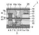
本発明の第1実施形態に係る相変化メモリ装置について説明する。図1に、本発明の第1実施形態に係る相変化メモリ装置の概略断面図を示す。相変化メモリ装置1は、基板2と、基板2に形成された選択能動素子3と、選択能動素子3上に配された導体層11と、導体層11上に配された制御絶縁層(第1絶縁層)13と、制御絶縁層13上に配された相変化層15と、制御絶縁層13上に配された第1電極16及び第2電極17と、相変化層15上に配されたビット線と、制御絶縁層13下に配される下部保護絶縁層10と、制御絶縁層13上に配される上部保護絶縁層14と、を備える。 A phase change memory device according to a first embodiment of the present invention will be described. FIG. 1 is a schematic cross-sectional view of a phase change memory device according to a first embodiment of the present invention. The phase
図2に、図1に示す相変化層の概略上面図を示す。図3に、図1のIII−III線における概略断面図を示す。線状の相変化層15は、第1電極16及び第2電極17により電流注入され、その電流により自己発熱して相変化する相変化領域15aを有する。相変化層15に給電する第1電極16及び第2電極17は、相変化層15に電気的に接続されているが、相変化領域15aに直接接してはいない。また、相変化領域15aは、制御絶縁層13と接して配されている。 FIG. 2 is a schematic top view of the phase change layer shown in FIG. FIG. 3 is a schematic sectional view taken along line III-III in FIG. The linear
相変化領域15aは、低電力かつ迅速に相変化するように、その電流通過方向に対して垂直な断面(図3に示す相変化領域15aの断面)の断面積を小さくすることが好ましい。一方、相変化領域15a以外の相変化層15の領域は、高抵抗化しないように相変化領域15aの断面積よりもその断面積を大きくすると好ましい。したがって、相変化領域15aは、相変化領域15a以外の領域よりも薄層化及び/又は細線化すると好ましい。相変化領域15aの体積(特に図3に示す断面積)は、所望の電力及び速度で情報の書き込みができるように設定する。また、相変化領域15aの厚さは、均一な層厚にできるように設定する。例えば、相変化領域15aの厚さd1は、1nm〜50nmとすることができる。また、相変化領域15a以外の相変化層15の領域の厚さd2は、50nm〜100nmとすることができる。
相変化領域15aの幅w1は、例えば、30nm〜200nmとすることができる。また、相変化領域15a以外の領域の幅w2は、相変化領域の幅w1の1倍〜3倍程度太くすることができる。Widthw 1 of the
相変化層15の材料としては、温度に応じて2以上の相状態を有し、かつ、相状態によって電気抵抗が異なる材料であればよく、例えば、カルコゲナイド材料を用いることができる。カルコゲン元素とは周期律表における6族に属する原子であり硫黄(S)、セレン(Se)、テルル(Te)のことを指す。一般的にカルコゲナイド材料とは、少なくとも1つのカルコゲン元素と共に、ゲルマニウム(Ge)、スズ(Sn)、アンチモン(Sb)のうち少なくとも1つの元素を含む化合物のことである。この際、窒素(N)、酸素(O)、銅(Cu)、アルミニウム(Al)等の元素が添加された材料を用いることもできる。例として、GaSb、InSb、InSe、Sb2Te3、GeTe等の2元系元素、Ge2Sb2Te5、InSbTe、GaSeTe、SnSb2Te4、InSbGe等の3元系元素、AgInSbTe、(GeSn)SbTe、GeSb(SeTe)、Te81Ge15Sb2S2等の4元系元素が挙げられる。The material of the
導体層11は、導体層11に伝導した熱を相変化メモリ装置1の外部に放熱できるように、外部と熱的に接続されていると好ましく、例えば選択能動素子3のGND配線層とすることができる。導体層11は、制御絶縁層13に接して配されている。相変化領域15aと導体層11とは、相変化領域15aの熱を導体層11に伝導できるように、制御絶縁層13を介して少なくとも一部が重複するように配されている。好ましくは、相変化領域15aの熱を効率よく導体層11に伝導できるように、図2に示すように上面から見た場合に、相変化領域15aの面積の80%〜100%が導体層11と重なるようにする。 The
導体層11の材料は、相変化領域15aの急冷速度を制御するために、所望の熱伝導率となるようなものを選択すると好ましい。一般的に、金属の電気抵抗率と熱伝導率は反比例関係にあることが知られており、電気抵抗率を制御することで熱伝導率を容易に算出することができる。例えば、導体層11の熱伝導率を高くしたい場合、アルミニウム(Al)、タングステン(W)等を使用することができ、導体層11の熱伝導率を低くしたい場合、窒化チタン(TiN)等の材料を使用することができる。また、窒化チタン(TiN)のような材料においては、CVD法を用いて導体層11を形成する場合、不純物の混入量等によって比較的簡単に電気抵抗率を制御することができる(例えば、抵抗率をおおよそ20μΩcmから1000μΩcmの範囲で変化させることができる)。 The material of the
導体層11は、単層でもよいが、図1に示すように、材料の異なる複数の層を積層して形成して、放熱制御することもできる。例えば、導体層11を選択能動素子3のGND配線層とした場合に、放熱性抑制の観点からGND配線層を熱伝導率の低い(すなわち電気抵抗率の高い)材料のみで形成すると、GND配線層の高抵抗化のために、GNDパッドとアレイ部との間に電位差が生じ、回路上問題が生じることになる。そこで、電気抵抗率の低い材料を積層することで、導体層11の高抵抗化を抑制することができる。単層が好ましい場合としては、例えば、導体層11に熱伝導率の高い材料を選択した場合である。異なる材料の積層が好ましい場合としては、例えば、放熱制御の観点から、制御絶縁層13と接する上部導体層11bに熱伝導率が低い材料を選択した場合である。この場合には、上部導体層11bの下層となる下部導体層11aに上部導体層11bよりも電気抵抗率が低い材料を選択することが好ましい。例えば、図1に示す形態においては、上部導体層11bとして厚さ10nmの窒化チタン(TiN)を使用し、下部導体層11aとして厚さ20nmのタングステン(W)を使用することができる。また、導体層11の高抵抗化の抑制は、寄生容量が問題とならない程度に導体層11の膜厚を厚くすることによっても実現することができる。導体層11全体の膜厚は、高抵抗化の抑制と寄生容量増大の防止の観点から、20nm〜60nmであると好ましい。 The
制御絶縁層13は、相変化領域15aの熱を導体層11に伝導する機能と共に、相変化層15と導体層11とを絶縁する機能も果たす。そのため、制御絶縁層13の厚さd3は、放熱制御の観点から設定すると共に、絶縁破壊しないように設定する。例えば、制御絶縁層13の厚さd3は、5nm〜30nmとすることができる。The
制御絶縁層13、下部保護絶縁層10及び上部保護絶縁層14の材料は、絶縁層として使用可能なものであれば特に制限されずに用いることができる。例えば、シリコン酸化物(SiO2)、シリコン窒化物(SiN)およびそれらの混合物などを用いることができる。また、場合によってはBPSG(Boro-Phospho silicate glass)等の低誘電率絶縁膜を用いてもよい。絶縁層は原子密度が高いほど熱伝導性が高くなるため、熱処理等を行いなるべく高原子密度となるよう形成すると好ましい。The material of the
制御絶縁層13、下部保護絶縁層10及び上部保護絶縁層14は、同じ材料を用いることもできるが、以下に説明する製造方法において選択的なエッチングができるように、制御絶縁層13と上部保護絶縁層14とは異なる材料で形成すると好ましい。また、下部保護絶縁層10及び上部保護絶縁層14は、寄生容量抑制の観点から低誘電率の材料(例えば酸化シリコン(SiO2)やBPSG)が好ましい。下部保護絶縁層10及び上部保護絶縁層14として、酸化シリコン(SiO2)やBPSGを用いた場合、制御絶縁層13としては、それ以外の材料(例えば窒化シリコン(SiN))を使用することができる。また、相変化領域15aには、情報書き換え時に高い電圧が印加されるので、制御絶縁層13は絶縁破壊耐性が高く、かつリーク電流が小さいと好ましい。この対策として、制御絶縁層13は、複数の絶縁材料の積層構造(例えばSiNとSiO2の積層構造)にすることもできる。The
第1電極16と第2電極17とは、間隔をあけて相変化層15に接続されるが、相変化領域15aはその間に配されるようにする。第1電極16及び第2電極17と相変化領域15aとの間隔(距離)は、第1電極16及び第2電極17と相変化領域15aとの間隔が近すぎると、第1電極16及び第2電極17からの放熱が大きくなりすぎ、相変化状態の適切な制御が困難となるので、第1電極16及び第2電極17からの放熱が大きくなりすぎないように設定すると好ましい。第1電極16及び第2電極17と相変化領域15aとの間隔をとる場合、相変化メモリ装置1が横方向(制御絶縁層13の延在方向)に大きくならないように、相変化領域15aと第1電極16及び第2電極17とで高低差をつけると好ましい。例えば、相変化層15は、図1に示すような断面において、凹状に形成すると好ましい。すなわち、相変化層15に凹部又は溝部15bを形成し、相変化層15の凹部又は溝部15bの底部に相変化領域15aが形成され、凹部又は溝部15bの上部に第1電極16及び第2電極17を電気的に接続すると好ましい。主として導体層11からの放熱制御を支配的にする場合、相変化領域15aと第1電極16及び第2電極17との上下方向の間隔は、相変化領域15aと導体層11との間隔(すなわち制御絶縁層13の厚さd3)の3倍以上であると好ましい。The
相変化層15と第1電極16又は第2電極17との接触面積は、相変化領域15aの面積に対して十分大きいと好ましく、例えば約2〜5倍であると好ましい。 The contact area between the
図1に示す形態のように、相変化層15を凹状に形成する(相変化層に複数の凹部又は溝部15bを形成する)場合、以下に製造方法について説明するように、相変化領域15aのみを選択的に薄膜化することができる。 When the
図1に示す形態においては、第1電極16及び第2電極17の下面は、上部保護絶縁層14に接しており、相変化層15は、その第1電極16及び第2電極17を覆うように形成されている。この形態の場合、以下に製造方法について説明するように、相変化層15を形成する前に第1電極16及び第2電極17を形成することができるので、第1電極16及び第2電極17の形成時に相変化層15の上面にダメージを与えずにすむ。 In the form shown in FIG. 1, the lower surfaces of the
第1電極16及び第2電極17の一方は、第3コンタクト18を介してビット線19と電気的に接続され、他方は、コンタクトプラグ12及び第1コンタクト8を介して、選択能動素子3の第1拡散層4と電気的に接続されている。 One of the
第1電極16及び第2電極17の材料としては、公知の電極材料であれば特に制限なく用いることができる。例えば、チタン(Ti)、タンタル(Ta)、モリブデン(Mo)、ニオブ(Nb)、ジルコニウム(Zr)若しくはタングステン(W)、またはこれらの金属の窒化物、あるいはこれらの金属およびその窒化物を含むシリサイド化合物などを用いることができる。また、前記金属を含む合金を用いることができる。なお、電極材料を形成する窒化物やシリサイド等の化合物は化学量論比である必要はない。また、前記電極材料には炭素(C)等の不純物を添加することもできる。 As materials for the
選択能動素子3(本実施形態においてはMOSトランジスタ)は、相変化領域15a等の下方に配されている。選択能動素子3は、第1拡散層(例えばドレイン拡散層)4、第2拡散層(例えばソース拡散層)5、ゲート絶縁膜7、及びワード線となるゲート電極6を有している。第1拡散層4は、第1コンタクト8及びコンタクトプラグ12を介して第1電極16に電気的に接続され、第2拡散層5は、第2コンタクト9を介して導体層11と電気的に接続されている。 The selective active element 3 (in this embodiment, a MOS transistor) is disposed below the
本実施形態によれば、導体層11を選択能動素子3のGND配線層として使用すると共に、相変化領域15aのヒートシンクとしても使用することができる。また、本発明によれば、選択能動素子3をメモリ部25の下方に配することができ、選択能動素子3とメモリ部25とを横方向に並べて配置する形態よりも面積効率を高めることができ、高集積化を図ることができる。さらに、選択能動素子3とメモリ部25とを横方向に並べて配置する形態よりも製造工程を削減することができ、製造コストを削減することができる。 According to this embodiment, the
第1コンタクト8、第2コンタクト9、第3コンタクト18及びコンタクトプラグ12の材料としては、コンタクトとして使用可能な材料であればいずれの材料を使用することができ、例えばアルミニウム(Al)やタングステン(W)を使用することができる。 As the material of the
本発明の相変化メモリ装置1において、相変化領域15aの熱は、制御絶縁層13を通じて導体層11に伝導し、導体層11がヒートシンクとして作用する。この放熱特性は、導体層11の材料、形状、寸法等、及び制御絶縁層13の材料、寸法等により調整することができ、これにより、リセット動作における冷却速度を制御することができる。 In the phase
なお、図1に示す形態においては、第2拡散層5の真上に相変化領域15aが配されているが、相変化領域15aと導体層11の少なくとも一部が重なるように配されていれば、図1に示す形態に限定されるものではない。 In the embodiment shown in FIG. 1, the
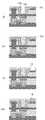
次に、本発明の第1実施形態に係る相変化メモリ装置の製造方法について説明する。図4〜図7に、第1実施形態に係る相変化メモリ装置の製造方法を説明するための概略工程図を示す。 Next, a method for manufacturing the phase change memory device according to the first embodiment of the present invention will be described. 4 to 7 are schematic process diagrams for explaining the method of manufacturing the phase change memory device according to the first embodiment.
まず、基板2に選択能動素子3を形成する。選択能動素子3は、例えば、一般的なDRAMメモリセルにおけるセルトランジスタと同様の方法で作成することができ、その寸法は微細化のトレンドにしたがって決定される。次に、選択能動素子3上に下部保護絶縁層10の一部10aを形成する。次に、第1拡散層4及び第2拡散層5上に、例えばリソグラフィ技術を用いて下部保護絶縁層10の一部10aを第1拡散層4及び第2拡散層5が露出するまで等方性エッチングし、コンタクトホール10bを形成する(図4(a))。 First, the selective
次に、コンタクトホール10b内に、スパッタリング法等により第1コンタクト8及び第2コンタクト9を形成し、その表面を平坦化する(図4(b))。 Next, the
次に、下部保護絶縁層10の一部10cをスパッタリング法などによりさらに堆積する。次に、リソグラフィ技術を用いて、下部絶縁層10の一部10cを第2コンタクト9が露出するまで等方性エッチングし、下部絶縁層10の一部10cに導体層11のパターンからなる溝を形成する。この溝に導体層11をスパッタリング法等によって堆積する。導体層11を2層構造にする場合、下部導体層11aを堆積した後、その上に上部導体層11bを堆積する(図4(c))。 Next, a
次に、導体層11等の上に、スパッタリング法等により制御絶縁層13を堆積する。さらに、制御絶縁層13の上層に、上部保護絶縁層14のうちの第2絶縁層14aを積層し、CMP法等を用いて平坦化する(図4(d))。このとき、上部保護絶縁層14の選択的エッチングができるように、制御絶縁膜13の材料と上部保護絶縁層14の材料とは異なるものを選択する。これにより、後の工程において、制御絶縁膜13の膜厚を大きく変化させることなく、上部保護絶縁層14のみをエッチングすることができ、制御絶縁膜13の膜厚制御が容易となる。 Next, the
次に、第2コンタクト8の上面が露出するように上部保護絶縁層14の第2絶縁層14a、制御絶縁層13及び下部保護絶縁層10の一部10cを、リソグラフィ技術を用いて選択エッチングし、コンタクトホール21を形成する(図4(e))。 Next, the second insulating
次に、コンタクトホール21に、コンタクトプラグ12を堆積し、その表面を平坦化する(図5(f))。 Next, the
次に、第1電極16及び第2電極17の材料をスパッタリング法やCVD法等により堆積し、リソグラフィ技術用いて第1電極16及び第2電極17の材料の堆積層を等方性エッチングして、所定の位置に第1電極16及び第2電極17を形成する。このとき、第1電極16は、コンタクトプラグ12上に形成する(図5(g))。 Next, the materials of the
次に、第1電極16と第2電極17の間の上部保護絶縁層14の第2絶縁層14aをリソグラフィ技術を用いて制御絶縁層13が露出するまで選択エッチングし、第2絶縁層14a及び制御絶縁層13からなる溝部又は凹部(以下「凹部」と表記する)14bを形成する(図5(h))。このとき、凹部14bの底面、すなわち制御絶縁層13が露出する領域の少なくとも一部は、導体層11の形成領域と重複するようにする。好ましくは、導体層11の真上にある制御絶縁層13の領域が露出するようにする。 Next, the second insulating
次に、凹部14b内、上部保護絶縁層14上、及び第1電極16及び第2電極17上に、相変化層15の材料をスパッタリング法等により堆積する(図5(i))。 Next, the material of the
次に、堆積させた相変化層15の材料を、リソグラフィ技術を用いて凹部14b内に相変化層15の凹部15bを形成するように異方性エッチングする(図6(j))。このとき、凹部15bの底面領域が、導体層11の真上に掛かるようし、この領域が相変化領域15aとなる。エッチングは、相変化領域15aが所定の厚さになるまで実施する。 Next, the deposited material of the
次に、堆積した相変化層15の材料を、リソグラフィ技術を用いて線状にエッチングして、相変化層15を形成する。このとき、上部保護絶縁層14として用いることができる材料(例えば酸化シリコン(SiO2)等)をハードマスクとして使用することができる。この場合、ハードマスクを除去する工程を削除することができる。また、相変化層15の上面をエッチングする必要がないので、相変化層15に与えるダメージを少なくすることができる。Next, the
次に、相変化層15の上に、上部保護絶縁層14の第3絶縁層14cを堆積し、CMP法等を用いて平坦化する(図6(k))。 Next, a third insulating
次に、第2電極17の少なくとも一部が露出するように、上部保護絶縁層14の第3絶縁層14c及び相変化層15をリソグラフィ技術を用いて選択エッチングして、コンタクトホール22を形成する(図6(l))。 Next, the third insulating
次に、第3コンタクト18の材料をコンタクトホール22内に堆積して、その表面を平坦化し、第3コンタクト18を形成する(図6(m))。 Next, the material of the
次に、上部保護絶縁層14の第4絶縁層14dを堆積する(図7(n))。次に、堆積した第4絶縁層14dの一部を、リソグラフィ技術を用いて第3コンタクト18が露出するように異方性エッチングして、ビット線を配する溝部又は凹部を形成する(不図示)。 Next, a fourth insulating
次に、第4絶縁層14dに形成した凹部又は溝部にビット線19の材料を堆積し、CMP法等を用いて平坦化して、ビット線19を形成する(図7(o))。 Next, the material of the
次に、上部保護絶縁層14の第5絶縁層14eを堆積して、相変化メモリ装置1を形成する(図7(p))。 Next, the fifth insulating
次に、公知の方法を用いて周辺回路を形成して、相変化メモリ装置1をメモリセルとして有する半導体メモリ装置を形成する(不図示)。 Next, a peripheral circuit is formed by using a known method to form a semiconductor memory device having the phase
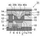
次に、本発明の第2実施形態に係る相変化メモリ装置について説明する。図8に、本発明の第2実施形態に係る相変化メモリ装置の概略断面図を示す。なお、図8において、図1と同じ要素には同じ符号を付してある。本実施形態において、第1実施形態と異なる点は、相変化メモリ装置31がサイドウォール40を有し、相変化層35の形態が異なることである。 Next, a phase change memory device according to a second embodiment of the present invention will be described. FIG. 8 is a schematic cross-sectional view of a phase change memory device according to the second embodiment of the present invention. In FIG. 8, the same elements as those in FIG. The present embodiment is different from the first embodiment in that the phase
サイドウォール40は、相変化領域35aの両側に沿って形成されており、サイドウォール40と制御絶縁層13とで溝部又は凹部(以下「凹部」と表記する)40aを形成している。サイドウォール40は、凹部40aの底面から上方に向かって凹部40aの幅を拡げるような曲面を有する。 The
相変化領域35aは、凹部40aの底面に沿って(好ましくは制御絶縁層13に接して)形成されている。相変化層35は、サイドウォール40の曲面上を相変化領域35aと連続して延在し、凹部40aの底面から上方に向かって層厚が次第に厚くなっている層厚変化領域35bをさらに有し、上部保護絶縁層14上において最も層厚が厚くなっている。 The
サイドウォール40の材料としては、絶縁体であってもよく、または金属であってもよい。サイドウォール40として絶縁体を用いる場合は、制御絶縁層13に対して選択的エッチングできるように、制御絶縁層13と異なる材料を用いると好ましい。 The material of the
サイドウォール40を形成することにより、スパッタリング法による相変化層35の堆積において、エッチング工程を実施しなくても薄層化した相変化領域35aを得ることができる。すなわち、本実施形態によれば、エッチングによるダメージが与えられていない相変化領域35aを得ることができる By forming the
第2実施形態における上記以外の形態は、第1実施形態と同様であり、ここでの説明は省略する。 Other aspects of the second embodiment are the same as those of the first embodiment, and a description thereof is omitted here.
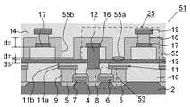
次に、本発明の第3実施形態に係る相変化メモリ装置について説明する。図9に、本発明の第3実施形態に係る相変化メモリ装置の概略断面図を示す。図9において、図1と同じ要素には同じ符号を付してある。第1実施形態においては、1つのメモリ部に対して1つの選択能動素子が形成されていたが、本実施形態においては、隣接する2つのメモリ部が選択能動素子を共有している。 Next, a phase change memory device according to a third embodiment of the invention will be described. FIG. 9 is a schematic cross-sectional view of a phase change memory device according to a third embodiment of the present invention. In FIG. 9, the same elements as those of FIG. In the first embodiment, one selective active element is formed for one memory unit. However, in this embodiment, two adjacent memory units share the selective active element.
相変化層55は、複数の相変化領域55aを有している。例えば、線状の相変化層55には、複数の凹部又は溝部55bが連続的に形成され、図9に示す断面全体において、相変化層55はミアンダ状(又は波形状)に形成されている。第1実施形態と同様に、相変化領域55aは、凹部又は溝部55bの底部に形成されている。
各相変化領域55aの下に導体層11が配されている。図9に示す形態においては、導体層11は、選択能動素子53のGND配線層であり、導体層11下には、第2コンタクト9によって導体層11と電気的に接続された第2拡散層5が形成されている。隣接する2つの第2拡散層5の間には、隣接する第2拡散層5に共有される第1拡散層4が形成されている。第1拡散層4は、第1コンタクト8及びコンタクトプラグ12を介して第1電極16と電気的に接続されている。第1電極16と第2電極17は、第1電極16と第2電極17とで1つの相変化領域55aを挟むように相変化層55に接続されている。すなわち、相変化層55において、第1電極16と第2電極17は交互に連続的に配され、第1電極16と第2電極17との間に相変化領域55aが形成されている。なお、図9において、ワード線6とビット線19とは、上面からみると直交するように延在している。例えば、図9に示す断面に対して、ワード線6が45°方向に延在し、ビット線19が135°方向に延在する。
第3実施形態における上記以外の形態は、第1実施形態と同様であり、ここでの説明は省略する。また、第3実施形態は、第2実施形態と組み合わせることもできる。 Other aspects of the third embodiment are the same as those of the first embodiment, and a description thereof is omitted here. In addition, the third embodiment can be combined with the second embodiment.
本発明の相変化メモリ装置及びその製造方法は、上記実施形態に基づいて説明されているが、上記実施形態に限定されることなく、本発明の範囲内において、かつ本発明の基本的技術思想に基づいて、上記実施形態に対し種々の変形、変更及び改良を含むことができることはいうまでもない。また、本発明の請求の範囲の枠内において、種々の開示要素の多様な組み合わせ・置換ないし選択が可能である。 The phase change memory device and the manufacturing method thereof according to the present invention have been described based on the above embodiment, but are not limited to the above embodiment, and are within the scope of the present invention and the basic technical idea of the present invention. It goes without saying that various modifications, changes and improvements can be included in the above embodiment based on the above. Further, various combinations, substitutions, or selections of various disclosed elements are possible within the scope of the claims of the present invention.
本発明のさらなる課題、目的及び展開形態は、請求の範囲を含む本発明の全開示事項からも明らかにされる。 Further problems, objects, and developments of the present invention will become apparent from the entire disclosure of the present invention including the claims.
1,31,51 相変化メモリ装置
2 基板
3,53 選択能動素子
4 第1拡散層
5 第2拡散層
6 ゲート電極(ワード線)
7 ゲート絶縁膜
8 第1コンタクト
9 第2コンタクト
10 下部保護絶縁層
10a 下部保護絶縁層の一部
10b コンタクトホール
10c 下部保護絶縁層の一部
11 導体層
11a 下部導体層
11b 上部導体層
12 コンタクトプラグ
13 制御絶縁層(第1絶縁層)
14 上部保護絶縁層
14a 第2絶縁層
14b 溝部又は凹部
14c 第3絶縁層
14d 第4絶縁層
14e 第5絶縁層
15,35,55 相変化層
15a,35a,55a 相変化領域
15b,55b 凹部又は溝部
35b 層厚変化領域
16 第1電極
17 第2電極
18 第3コンタクト
19 ビット線
21,22 コンタクトホール
25 メモリ部
40 サイドウォール
40a 溝部又は凹部1, 31, 51 Phase
7
14 upper protective insulating
Claims (21)
Translated fromJapanese前記相変化領域の下に配される第1絶縁層と、
前記第1絶縁層の下に配される導体層と、を備え、
前記相変化領域及び前記導体層は、前記相変化領域の熱が前記第1絶縁層を介して前記導体層に伝導するように配されていることを特徴とする相変化メモリ装置。A phase change region;
A first insulating layer disposed under the phase change region;
A conductor layer disposed under the first insulating layer,
The phase change memory device, wherein the phase change region and the conductor layer are arranged so that heat of the phase change region is conducted to the conductor layer through the first insulating layer.
前記相変化領域の下に、前記相変化領域に接して配される第1絶縁層と、
前記第1絶縁層の下に前記第1絶縁層に接して配されると共に、少なくとも一部が前記相変化領域の真下に配される導体層と、を備え、
前記導体層は、前記相変化領域のヒートシンクとして作用することを特徴とする相変化メモリ装置。A phase change region;
A first insulating layer disposed under and in contact with the phase change region;
A conductive layer disposed under and in contact with the first insulating layer under the first insulating layer, and at least a portion disposed directly under the phase change region;
The phase change memory device, wherein the conductor layer acts as a heat sink for the phase change region.
前記相変化層に電気的に接続され、前記相変化領域に給電する第1電極及び第2電極と、をさらに備え、
前記相変化領域は、前記相変化層の一部であり、
前記第1電極と前記第2電極との間に前記相変化領域が配されていることを特徴とする請求項1〜3のいずれか一項に記載の相変化メモリ装置。A phase change layer;
A first electrode and a second electrode electrically connected to the phase change layer and supplying power to the phase change region;
The phase change region is part of the phase change layer;
The phase change memory device according to claim 1, wherein the phase change region is disposed between the first electrode and the second electrode.
前記相変化領域は、前記相変化層の前記溝部又は凹部の底部に形成され、
前記第1電極及び前記第2電極は、前記相変化領域を挟むように前記溝部又は凹部の上部に形成されていることを特徴とする請求項4に記載の相変化メモリ装置。The phase change layer has a groove or a recess,
The phase change region is formed at the bottom of the groove or recess of the phase change layer,
5. The phase change memory device according to claim 4, wherein the first electrode and the second electrode are formed on an upper portion of the groove or the recess so as to sandwich the phase change region. 6.
前記相変化層は、延在方向に垂直な断面においてミアンダ状又は波形状に形成されていることを特徴とする請求項5に記載の相変化メモリ装置。The phase change layer has a plurality of the phase change regions,
6. The phase change memory device according to claim 5, wherein the phase change layer is formed in a meander shape or a wave shape in a cross section perpendicular to the extending direction.
前記第1電極及び前記第2電極は、前記第2絶縁層より上に配されていることを特徴とする請求項5又は6に記載の相変化メモリ装置。A second insulating layer on the first insulating layer;
7. The phase change memory device according to claim 5, wherein the first electrode and the second electrode are disposed above the second insulating layer. 8.
前記第1絶縁層及び前記第2絶縁層は溝部又は凹部を有し、
前記相変化領域は、前記凹部の底面に沿って形成されていることを特徴とする請求項9に記載の相変化メモリ装置。A second insulating layer on the first insulating layer;
The first insulating layer and the second insulating layer have a groove or a recess,
The phase change memory device according to claim 9, wherein the phase change region is formed along a bottom surface of the recess.
前記サイドウォールは、前記溝部又は凹部の底面から上方に向かって前記溝部又は凹部の幅を拡げるような曲面を有し、
前記層厚変化領域は、前記曲面上に形成されていることを特徴とする請求項10又は11に記載の相変化メモリ装置。Further comprising sidewalls formed along both side surfaces of the groove or recess,
The sidewall has a curved surface that widens the width of the groove or recess upward from the bottom surface of the groove or recess,
The phase change memory device according to claim 10, wherein the layer thickness change region is formed on the curved surface.
前記上部導体層は、前記下部導体層よりも熱伝導率が高いことを特徴とする請求項1〜16のいずれか一項に記載の相変化メモリ装置。The conductor layer has an upper conductor layer disposed in contact with the first insulating layer, and a lower conductor layer laminated under the upper conductor layer,
The phase change memory device according to claim 1, wherein the upper conductor layer has higher thermal conductivity than the lower conductor layer.
前記導体層は、前記選択能動素子のGND配線層であることを特徴とする請求項1〜17のいずれか一項に記載の相変化メモリ装置。A selective active element is further provided below the conductor layer,
The phase change memory device according to claim 1, wherein the conductor layer is a GND wiring layer of the selective active element.
前記選択能動素子は、第1拡散層、第2拡散層、及びゲート電極を有するトランジスタであり、
前記第1拡散層は、前記第1電極と電気的に接続され、
前記第2拡散層は、前記導体層と電気的に接続され、
前記第2電極は、前記ビット線と電気的に接続されることを特徴とする請求項1〜18のいずれか一項に記載の相変化メモリ装置。A bit line is further provided above the phase change layer,
The selective active element is a transistor having a first diffusion layer, a second diffusion layer, and a gate electrode,
The first diffusion layer is electrically connected to the first electrode;
The second diffusion layer is electrically connected to the conductor layer;
The phase change memory device according to claim 1, wherein the second electrode is electrically connected to the bit line.
前記導体層上に、第1絶縁層を形成する工程と、
前記第1絶縁層上に、第2絶縁層を形成する工程と、
前記第2絶縁層上に、第1電極及び第2電極を形成する工程と、
前記第2絶縁層、前記第1電極及び前記第2電極上に、相変化層を形成する工程と、を含むことを特徴とする相変化メモリ装置の製造方法。Forming a conductor layer;
Forming a first insulating layer on the conductor layer;
Forming a second insulating layer on the first insulating layer;
Forming a first electrode and a second electrode on the second insulating layer;
Forming a phase change layer on the second insulating layer, the first electrode, and the second electrode. A method of manufacturing a phase change memory device, comprising:
前記第1絶縁層の露出した領域にも前記相変化層を形成した後に、前記第1絶縁層と接している前記相変化層の一部を薄膜化する工程と、をさらに含むことを特徴とする請求項20に記載の相変化メモリ装置の製造方法。Removing a part of the second insulating layer so that at least a part of a region of the first insulating layer on the conductor layer is exposed before forming the phase change layer;
Further comprising a step of thinning a part of the phase change layer in contact with the first insulating layer after forming the phase change layer also in the exposed region of the first insulating layer. 21. A method of manufacturing a phase change memory device according to claim 20.
Priority Applications (1)
| Application Number | Priority Date | Filing Date | Title |
|---|---|---|---|
| JP2008251166AJP2010087007A (en) | 2008-09-29 | 2008-09-29 | Phase change memory device and method of manufacturing the same |
Applications Claiming Priority (1)
| Application Number | Priority Date | Filing Date | Title |
|---|---|---|---|
| JP2008251166AJP2010087007A (en) | 2008-09-29 | 2008-09-29 | Phase change memory device and method of manufacturing the same |
Publications (1)
| Publication Number | Publication Date |
|---|---|
| JP2010087007Atrue JP2010087007A (en) | 2010-04-15 |
Family
ID=42250723
Family Applications (1)
| Application Number | Title | Priority Date | Filing Date |
|---|---|---|---|
| JP2008251166APendingJP2010087007A (en) | 2008-09-29 | 2008-09-29 | Phase change memory device and method of manufacturing the same |
Country Status (1)
| Country | Link |
|---|---|
| JP (1) | JP2010087007A (en) |
Cited By (12)
| Publication number | Priority date | Publication date | Assignee | Title |
|---|---|---|---|---|
| KR20150133658A (en)* | 2014-05-20 | 2015-11-30 | 크로스바, 인크. | Resistive memory architecture and devices |
| US9431610B2 (en) | 2012-06-01 | 2016-08-30 | Samsung Electronics Co., Ltd. | Methods of manufacturing a phase change memory device including a heat sink |
| US9633724B2 (en) | 2014-07-07 | 2017-04-25 | Crossbar, Inc. | Sensing a non-volatile memory device utilizing selector device holding characteristics |
| US9685483B2 (en) | 2014-07-09 | 2017-06-20 | Crossbar, Inc. | Selector-based non-volatile cell fabrication utilizing IC-foundry compatible process |
| US9698201B2 (en) | 2014-07-09 | 2017-07-04 | Crossbar, Inc. | High density selector-based non volatile memory cell and fabrication |
| US9761635B1 (en) | 2014-03-11 | 2017-09-12 | Crossbar, Inc. | Selector device for two-terminal memory |
| US10096362B1 (en) | 2017-03-24 | 2018-10-09 | Crossbar, Inc. | Switching block configuration bit comprising a non-volatile memory cell |
| US10115819B2 (en) | 2015-05-29 | 2018-10-30 | Crossbar, Inc. | Recessed high voltage metal oxide semiconductor transistor for RRAM cell |
| US10211397B1 (en) | 2014-07-07 | 2019-02-19 | Crossbar, Inc. | Threshold voltage tuning for a volatile selection device |
| US10210929B1 (en) | 2014-07-09 | 2019-02-19 | Crossbar, Inc. | Non-volatile memory cell utilizing volatile switching two terminal device and a MOS transistor |
| CN112635667A (en)* | 2020-12-30 | 2021-04-09 | 上海集成电路装备材料产业创新中心有限公司 | Phase change memory unit and preparation method thereof |
| CN113930219A (en)* | 2021-10-25 | 2022-01-14 | 贵州理工学院 | A kind of micro-current self-heating plate for battery thermal management and preparation method thereof |
Citations (3)
| Publication number | Priority date | Publication date | Assignee | Title |
|---|---|---|---|---|
| JP2007080978A (en)* | 2005-09-12 | 2007-03-29 | Elpida Memory Inc | Phase change memory element, phase change memory IC, method of manufacturing phase change memory element, and method of manufacturing phase change memory IC |
| JP2007513494A (en)* | 2003-10-23 | 2007-05-24 | ライニッシュ−ヴェストフェリッシェ・テクニッシェ・ホッホシューレ・アーヘン | Phase change memory, phase change memory assembly, phase change memory cell, 2D phase change memory cell array, 3D phase change memory cell array, and electronic component |
| JP2008529269A (en)* | 2005-01-25 | 2008-07-31 | エヌエックスピー ビー ヴィ | Fabrication of phase change resistors using back-end processes |
- 2008
- 2008-09-29JPJP2008251166Apatent/JP2010087007A/enactivePending
Patent Citations (3)
| Publication number | Priority date | Publication date | Assignee | Title |
|---|---|---|---|---|
| JP2007513494A (en)* | 2003-10-23 | 2007-05-24 | ライニッシュ−ヴェストフェリッシェ・テクニッシェ・ホッホシューレ・アーヘン | Phase change memory, phase change memory assembly, phase change memory cell, 2D phase change memory cell array, 3D phase change memory cell array, and electronic component |
| JP2008529269A (en)* | 2005-01-25 | 2008-07-31 | エヌエックスピー ビー ヴィ | Fabrication of phase change resistors using back-end processes |
| JP2007080978A (en)* | 2005-09-12 | 2007-03-29 | Elpida Memory Inc | Phase change memory element, phase change memory IC, method of manufacturing phase change memory element, and method of manufacturing phase change memory IC |
Cited By (24)
| Publication number | Priority date | Publication date | Assignee | Title |
|---|---|---|---|---|
| US9431610B2 (en) | 2012-06-01 | 2016-08-30 | Samsung Electronics Co., Ltd. | Methods of manufacturing a phase change memory device including a heat sink |
| KR101934003B1 (en) | 2012-06-01 | 2019-01-02 | 삼성전자주식회사 | Phase change memory devices and methods of manufacturing the same |
| US10121540B1 (en) | 2014-03-11 | 2018-11-06 | Crossbar, Inc. | Selector device for two-terminal memory |
| US9847130B1 (en) | 2014-03-11 | 2017-12-19 | Crossbar, Inc. | Selector device for two-terminal memory |
| US11776626B2 (en) | 2014-03-11 | 2023-10-03 | Crossbar, Inc. | Selector device for two-terminal memory |
| US10964388B2 (en) | 2014-03-11 | 2021-03-30 | Crossbar, Inc. | Selector device for two-terminal memory |
| US9761635B1 (en) | 2014-03-11 | 2017-09-12 | Crossbar, Inc. | Selector device for two-terminal memory |
| JP2015220465A (en)* | 2014-05-20 | 2015-12-07 | クロスバー, インコーポレイテッドCrossbar, Inc. | Resistive memory architecture and apparatus |
| US9768234B2 (en) | 2014-05-20 | 2017-09-19 | Crossbar, Inc. | Resistive memory architecture and devices |
| KR102407740B1 (en)* | 2014-05-20 | 2022-06-10 | 크로스바, 인크. | Resistive memory architecture and devices |
| KR20150133658A (en)* | 2014-05-20 | 2015-11-30 | 크로스바, 인크. | Resistive memory architecture and devices |
| US9633724B2 (en) | 2014-07-07 | 2017-04-25 | Crossbar, Inc. | Sensing a non-volatile memory device utilizing selector device holding characteristics |
| US10211397B1 (en) | 2014-07-07 | 2019-02-19 | Crossbar, Inc. | Threshold voltage tuning for a volatile selection device |
| US10079060B2 (en) | 2014-07-07 | 2018-09-18 | Crossbar, Inc. | Sensing a non-volatile memory device utilizing selector device holding characteristics |
| US10210929B1 (en) | 2014-07-09 | 2019-02-19 | Crossbar, Inc. | Non-volatile memory cell utilizing volatile switching two terminal device and a MOS transistor |
| US9698201B2 (en) | 2014-07-09 | 2017-07-04 | Crossbar, Inc. | High density selector-based non volatile memory cell and fabrication |
| US9685483B2 (en) | 2014-07-09 | 2017-06-20 | Crossbar, Inc. | Selector-based non-volatile cell fabrication utilizing IC-foundry compatible process |
| US10115819B2 (en) | 2015-05-29 | 2018-10-30 | Crossbar, Inc. | Recessed high voltage metal oxide semiconductor transistor for RRAM cell |
| US10096362B1 (en) | 2017-03-24 | 2018-10-09 | Crossbar, Inc. | Switching block configuration bit comprising a non-volatile memory cell |
| US10541025B2 (en) | 2017-03-24 | 2020-01-21 | Crossbar, Inc. | Switching block configuration bit comprising a non-volatile memory cell |
| CN112635667A (en)* | 2020-12-30 | 2021-04-09 | 上海集成电路装备材料产业创新中心有限公司 | Phase change memory unit and preparation method thereof |
| CN112635667B (en)* | 2020-12-30 | 2022-11-25 | 上海集成电路装备材料产业创新中心有限公司 | A kind of phase-change memory unit and preparation method thereof |
| CN113930219A (en)* | 2021-10-25 | 2022-01-14 | 贵州理工学院 | A kind of micro-current self-heating plate for battery thermal management and preparation method thereof |
| CN113930219B (en)* | 2021-10-25 | 2023-04-28 | 贵州理工学院 | Micro-current self-heating flat plate for battery thermal management and preparation method thereof |
Similar Documents
| Publication | Publication Date | Title |
|---|---|---|
| US8129709B2 (en) | Nonvolatile memory device | |
| JP2010087007A (en) | Phase change memory device and method of manufacturing the same | |
| CN100559623C (en) | Non-volatile memory element and manufacture method thereof | |
| CN100541810C (en) | Electrically rewritable nonvolatile memory element and manufacturing method thereof | |
| US7808816B2 (en) | Semiconductor memory device and method for fabricating semiconductor memory device | |
| US7977674B2 (en) | Phase change memory device and method of fabricating the same | |
| CN103872067B (en) | Variable resistance memory device and its manufacturing method | |
| US9893281B2 (en) | Semiconductor device and method of fabricating the same | |
| TWI446528B (en) | Phase-change memory element and method for fabricating the same | |
| US8686393B2 (en) | Integrated circuit semiconductor devices including channel trenches and related methods of manufacturing | |
| JP4577692B2 (en) | Nonvolatile memory device and manufacturing method thereof | |
| JP2009206418A (en) | Nonvolatile memory device and manufacturing method for the same | |
| WO2011086725A1 (en) | Nonvolatile storage device and manufacturing method therefor | |
| WO2010140210A1 (en) | Semiconductor memory device and manufacturing method thereof | |
| JP2011103323A (en) | Semiconductor memory device | |
| CN103137863A (en) | Phase-change random access memory device and method of manufacturing the same | |
| JP5634002B2 (en) | Phase change nonvolatile memory and semiconductor device | |
| US20080186762A1 (en) | Phase-change memory element | |
| KR100946700B1 (en) | Phase change memory device and manufacturing method thereof | |
| US20090101885A1 (en) | Method of producing phase change memory device | |
| JP5579362B2 (en) | Method for manufacturing vertical phase change memory device | |
| KR20100055102A (en) | Variable resistance memory device, method of forming the same and memory system including the same | |
| JP2010087008A (en) | Nonvolatile memory device and method of manufacturing the same | |
| KR20250112592A (en) | Resistance variable memory device and method for fabricating the same | |
| KR20100076631A (en) | Phase change randomm access memory device and manufacturing method thereof |
Legal Events
| Date | Code | Title | Description |
|---|---|---|---|
| A621 | Written request for application examination | Free format text:JAPANESE INTERMEDIATE CODE: A621 Effective date:20110705 | |
| A711 | Notification of change in applicant | Free format text:JAPANESE INTERMEDIATE CODE: A711 Effective date:20130730 | |
| A131 | Notification of reasons for refusal | Free format text:JAPANESE INTERMEDIATE CODE: A131 Effective date:20131217 | |
| A977 | Report on retrieval | Free format text:JAPANESE INTERMEDIATE CODE: A971007 Effective date:20131219 | |
| A601 | Written request for extension of time | Free format text:JAPANESE INTERMEDIATE CODE: A601 Effective date:20140317 | |
| A602 | Written permission of extension of time | Free format text:JAPANESE INTERMEDIATE CODE: A602 Effective date:20140320 | |
| A601 | Written request for extension of time | Free format text:JAPANESE INTERMEDIATE CODE: A601 Effective date:20140325 | |
| A602 | Written permission of extension of time | Free format text:JAPANESE INTERMEDIATE CODE: A602 Effective date:20140328 | |
| A02 | Decision of refusal | Free format text:JAPANESE INTERMEDIATE CODE: A02 Effective date:20140819 |