JP2010080801A - Semiconductor device - Google Patents
Semiconductor deviceDownload PDFInfo
- Publication number
- JP2010080801A JP2010080801AJP2008249495AJP2008249495AJP2010080801AJP 2010080801 AJP2010080801 AJP 2010080801AJP 2008249495 AJP2008249495 AJP 2008249495AJP 2008249495 AJP2008249495 AJP 2008249495AJP 2010080801 AJP2010080801 AJP 2010080801A
- Authority
- JP
- Japan
- Prior art keywords
- lsi
- semiconductor device
- communication
- memory
- lsis
- Prior art date
- Legal status (The legal status is an assumption and is not a legal conclusion. Google has not performed a legal analysis and makes no representation as to the accuracy of the status listed.)
- Withdrawn
Links
Images


Classifications
- H—ELECTRICITY
- H01—ELECTRIC ELEMENTS
- H01L—SEMICONDUCTOR DEVICES NOT COVERED BY CLASS H10
- H01L25/00—Assemblies consisting of a plurality of semiconductor or other solid state devices
- H01L25/18—Assemblies consisting of a plurality of semiconductor or other solid state devices the devices being of the types provided for in two or more different main groups of the same subclass of H10B, H10D, H10F, H10H, H10K or H10N
- G—PHYSICS
- G11—INFORMATION STORAGE
- G11C—STATIC STORES
- G11C29/00—Checking stores for correct operation ; Subsequent repair; Testing stores during standby or offline operation
- G11C29/02—Detection or location of defective auxiliary circuits, e.g. defective refresh counters
- G—PHYSICS
- G11—INFORMATION STORAGE
- G11C—STATIC STORES
- G11C29/00—Checking stores for correct operation ; Subsequent repair; Testing stores during standby or offline operation
- G11C29/02—Detection or location of defective auxiliary circuits, e.g. defective refresh counters
- G11C29/025—Detection or location of defective auxiliary circuits, e.g. defective refresh counters in signal lines
- G—PHYSICS
- G11—INFORMATION STORAGE
- G11C—STATIC STORES
- G11C5/00—Details of stores covered by group G11C11/00
- G11C5/02—Disposition of storage elements, e.g. in the form of a matrix array
- H—ELECTRICITY
- H01—ELECTRIC ELEMENTS
- H01L—SEMICONDUCTOR DEVICES NOT COVERED BY CLASS H10
- H01L24/00—Arrangements for connecting or disconnecting semiconductor or solid-state bodies; Methods or apparatus related thereto
- H01L24/73—Means for bonding being of different types provided for in two or more of groups H01L24/10, H01L24/18, H01L24/26, H01L24/34, H01L24/42, H01L24/50, H01L24/63, H01L24/71
- H—ELECTRICITY
- H01—ELECTRIC ELEMENTS
- H01L—SEMICONDUCTOR DEVICES NOT COVERED BY CLASS H10
- H01L25/00—Assemblies consisting of a plurality of semiconductor or other solid state devices
- H01L25/03—Assemblies consisting of a plurality of semiconductor or other solid state devices all the devices being of a type provided for in a single subclass of subclasses H10B, H10D, H10F, H10H, H10K or H10N, e.g. assemblies of rectifier diodes
- H01L25/04—Assemblies consisting of a plurality of semiconductor or other solid state devices all the devices being of a type provided for in a single subclass of subclasses H10B, H10D, H10F, H10H, H10K or H10N, e.g. assemblies of rectifier diodes the devices not having separate containers
- H01L25/065—Assemblies consisting of a plurality of semiconductor or other solid state devices all the devices being of a type provided for in a single subclass of subclasses H10B, H10D, H10F, H10H, H10K or H10N, e.g. assemblies of rectifier diodes the devices not having separate containers the devices being of a type provided for in group H10D89/00
- H01L25/0657—Stacked arrangements of devices
- G—PHYSICS
- G11—INFORMATION STORAGE
- G11C—STATIC STORES
- G11C5/00—Details of stores covered by group G11C11/00
- G11C5/02—Disposition of storage elements, e.g. in the form of a matrix array
- G11C5/04—Supports for storage elements, e.g. memory modules; Mounting or fixing of storage elements on such supports
- H—ELECTRICITY
- H01—ELECTRIC ELEMENTS
- H01L—SEMICONDUCTOR DEVICES NOT COVERED BY CLASS H10
- H01L2224/00—Indexing scheme for arrangements for connecting or disconnecting semiconductor or solid-state bodies and methods related thereto as covered by H01L24/00
- H01L2224/01—Means for bonding being attached to, or being formed on, the surface to be connected, e.g. chip-to-package, die-attach, "first-level" interconnects; Manufacturing methods related thereto
- H01L2224/26—Layer connectors, e.g. plate connectors, solder or adhesive layers; Manufacturing methods related thereto
- H01L2224/31—Structure, shape, material or disposition of the layer connectors after the connecting process
- H01L2224/32—Structure, shape, material or disposition of the layer connectors after the connecting process of an individual layer connector
- H01L2224/321—Disposition
- H01L2224/32135—Disposition the layer connector connecting between different semiconductor or solid-state bodies, i.e. chip-to-chip
- H01L2224/32145—Disposition the layer connector connecting between different semiconductor or solid-state bodies, i.e. chip-to-chip the bodies being stacked
- H—ELECTRICITY
- H01—ELECTRIC ELEMENTS
- H01L—SEMICONDUCTOR DEVICES NOT COVERED BY CLASS H10
- H01L2224/00—Indexing scheme for arrangements for connecting or disconnecting semiconductor or solid-state bodies and methods related thereto as covered by H01L24/00
- H01L2224/01—Means for bonding being attached to, or being formed on, the surface to be connected, e.g. chip-to-package, die-attach, "first-level" interconnects; Manufacturing methods related thereto
- H01L2224/42—Wire connectors; Manufacturing methods related thereto
- H01L2224/47—Structure, shape, material or disposition of the wire connectors after the connecting process
- H01L2224/48—Structure, shape, material or disposition of the wire connectors after the connecting process of an individual wire connector
- H01L2224/4805—Shape
- H01L2224/4809—Loop shape
- H01L2224/48091—Arched
- H—ELECTRICITY
- H01—ELECTRIC ELEMENTS
- H01L—SEMICONDUCTOR DEVICES NOT COVERED BY CLASS H10
- H01L2224/00—Indexing scheme for arrangements for connecting or disconnecting semiconductor or solid-state bodies and methods related thereto as covered by H01L24/00
- H01L2224/01—Means for bonding being attached to, or being formed on, the surface to be connected, e.g. chip-to-package, die-attach, "first-level" interconnects; Manufacturing methods related thereto
- H01L2224/42—Wire connectors; Manufacturing methods related thereto
- H01L2224/47—Structure, shape, material or disposition of the wire connectors after the connecting process
- H01L2224/48—Structure, shape, material or disposition of the wire connectors after the connecting process of an individual wire connector
- H01L2224/481—Disposition
- H01L2224/48151—Connecting between a semiconductor or solid-state body and an item not being a semiconductor or solid-state body, e.g. chip-to-substrate, chip-to-passive
- H01L2224/48221—Connecting between a semiconductor or solid-state body and an item not being a semiconductor or solid-state body, e.g. chip-to-substrate, chip-to-passive the body and the item being stacked
- H01L2224/48225—Connecting between a semiconductor or solid-state body and an item not being a semiconductor or solid-state body, e.g. chip-to-substrate, chip-to-passive the body and the item being stacked the item being non-metallic, e.g. insulating substrate with or without metallisation
- H01L2224/48227—Connecting between a semiconductor or solid-state body and an item not being a semiconductor or solid-state body, e.g. chip-to-substrate, chip-to-passive the body and the item being stacked the item being non-metallic, e.g. insulating substrate with or without metallisation connecting the wire to a bond pad of the item
- H—ELECTRICITY
- H01—ELECTRIC ELEMENTS
- H01L—SEMICONDUCTOR DEVICES NOT COVERED BY CLASS H10
- H01L2225/00—Details relating to assemblies covered by the group H01L25/00 but not provided for in its subgroups
- H01L2225/03—All the devices being of a type provided for in the same main group of the same subclass of class H10, e.g. assemblies of rectifier diodes
- H01L2225/04—All the devices being of a type provided for in the same main group of the same subclass of class H10, e.g. assemblies of rectifier diodes the devices not having separate containers
- H01L2225/065—All the devices being of a type provided for in the same main group of the same subclass of class H10
- H01L2225/06503—Stacked arrangements of devices
- H01L2225/0651—Wire or wire-like electrical connections from device to substrate
- H—ELECTRICITY
- H01—ELECTRIC ELEMENTS
- H01L—SEMICONDUCTOR DEVICES NOT COVERED BY CLASS H10
- H01L2225/00—Details relating to assemblies covered by the group H01L25/00 but not provided for in its subgroups
- H01L2225/03—All the devices being of a type provided for in the same main group of the same subclass of class H10, e.g. assemblies of rectifier diodes
- H01L2225/04—All the devices being of a type provided for in the same main group of the same subclass of class H10, e.g. assemblies of rectifier diodes the devices not having separate containers
- H01L2225/065—All the devices being of a type provided for in the same main group of the same subclass of class H10
- H01L2225/06503—Stacked arrangements of devices
- H01L2225/06513—Bump or bump-like direct electrical connections between devices, e.g. flip-chip connection, solder bumps
- H—ELECTRICITY
- H01—ELECTRIC ELEMENTS
- H01L—SEMICONDUCTOR DEVICES NOT COVERED BY CLASS H10
- H01L2225/00—Details relating to assemblies covered by the group H01L25/00 but not provided for in its subgroups
- H01L2225/03—All the devices being of a type provided for in the same main group of the same subclass of class H10, e.g. assemblies of rectifier diodes
- H01L2225/04—All the devices being of a type provided for in the same main group of the same subclass of class H10, e.g. assemblies of rectifier diodes the devices not having separate containers
- H01L2225/065—All the devices being of a type provided for in the same main group of the same subclass of class H10
- H01L2225/06503—Stacked arrangements of devices
- H01L2225/06541—Conductive via connections through the device, e.g. vertical interconnects, through silicon via [TSV]
- H—ELECTRICITY
- H01—ELECTRIC ELEMENTS
- H01L—SEMICONDUCTOR DEVICES NOT COVERED BY CLASS H10
- H01L2225/00—Details relating to assemblies covered by the group H01L25/00 but not provided for in its subgroups
- H01L2225/03—All the devices being of a type provided for in the same main group of the same subclass of class H10, e.g. assemblies of rectifier diodes
- H01L2225/04—All the devices being of a type provided for in the same main group of the same subclass of class H10, e.g. assemblies of rectifier diodes the devices not having separate containers
- H01L2225/065—All the devices being of a type provided for in the same main group of the same subclass of class H10
- H01L2225/06503—Stacked arrangements of devices
- H01L2225/06572—Auxiliary carrier between devices, the carrier having an electrical connection structure
- H—ELECTRICITY
- H01—ELECTRIC ELEMENTS
- H01L—SEMICONDUCTOR DEVICES NOT COVERED BY CLASS H10
- H01L2924/00—Indexing scheme for arrangements or methods for connecting or disconnecting semiconductor or solid-state bodies as covered by H01L24/00
- H01L2924/01—Chemical elements
- H01L2924/01006—Carbon [C]
- H—ELECTRICITY
- H01—ELECTRIC ELEMENTS
- H01L—SEMICONDUCTOR DEVICES NOT COVERED BY CLASS H10
- H01L2924/00—Indexing scheme for arrangements or methods for connecting or disconnecting semiconductor or solid-state bodies as covered by H01L24/00
- H01L2924/01—Chemical elements
- H01L2924/01033—Arsenic [As]
- H—ELECTRICITY
- H01—ELECTRIC ELEMENTS
- H01L—SEMICONDUCTOR DEVICES NOT COVERED BY CLASS H10
- H01L2924/00—Indexing scheme for arrangements or methods for connecting or disconnecting semiconductor or solid-state bodies as covered by H01L24/00
- H01L2924/01—Chemical elements
- H01L2924/01082—Lead [Pb]
- H—ELECTRICITY
- H01—ELECTRIC ELEMENTS
- H01L—SEMICONDUCTOR DEVICES NOT COVERED BY CLASS H10
- H01L2924/00—Indexing scheme for arrangements or methods for connecting or disconnecting semiconductor or solid-state bodies as covered by H01L24/00
- H01L2924/15—Details of package parts other than the semiconductor or other solid state devices to be connected
- H01L2924/151—Die mounting substrate
- H01L2924/153—Connection portion
- H01L2924/1531—Connection portion the connection portion being formed only on the surface of the substrate opposite to the die mounting surface
- H01L2924/15311—Connection portion the connection portion being formed only on the surface of the substrate opposite to the die mounting surface being a ball array, e.g. BGA
- H—ELECTRICITY
- H01—ELECTRIC ELEMENTS
- H01L—SEMICONDUCTOR DEVICES NOT COVERED BY CLASS H10
- H01L2924/00—Indexing scheme for arrangements or methods for connecting or disconnecting semiconductor or solid-state bodies as covered by H01L24/00
- H01L2924/30—Technical effects
- H01L2924/301—Electrical effects
- H01L2924/3011—Impedance
Landscapes
- Engineering & Computer Science (AREA)
- Microelectronics & Electronic Packaging (AREA)
- Power Engineering (AREA)
- Computer Hardware Design (AREA)
- Physics & Mathematics (AREA)
- Condensed Matter Physics & Semiconductors (AREA)
- General Physics & Mathematics (AREA)
- Semiconductor Integrated Circuits (AREA)
Abstract
Translated fromJapaneseDescription
Translated fromJapanese本発明は、積層実装されたLSI群に関する。 The present invention relates to a group of stacked LSIs.
LSIは、微細加工技術の進化とともに、より多くのトランジスタを1チップに集積することで性能向上を図ってきた。しかしながら、微細化の限界や、最先端プロセスの利用コストの増大などの影響で、これまでのような1チップへの集積化を進めることが必ずしも最適解ではなくなる。そこで、複数のLSIを積層することによる3次元方向の集積が有望な技術となる。
このとき、積層されるLSI間および積層されたLSIの外部との通信機能が重要となる。積層LSIのための通信方式としては、有線方式(LSI基板シリコンに電極(穴)をあける方法など)、無線方式が検討されている。
昨今の高性能なメディア処理や、ネットワーク処理においては、CPUなどを含むプロセッサLSIとメモリ間の転送が年々大容量化しており、この部分の通信能力が全体の性能を決める主要因になってきている。特許文献1では、メモリとボード上の部品との通信を行うLSIと、複数のメモリLSIを積層した構成について言及している。システムボード上平面に実装されている複数のメモリを積層することでメモリへの配線を短くでき、高速化と低消費電力化に寄与する。With the advancement of microfabrication technology, LSIs have improved performance by integrating more transistors on a single chip. However, due to the limitations of miniaturization and the increase in the cost of using cutting-edge processes, it is not always the optimal solution to proceed with integration on a single chip. Therefore, three-dimensional integration by stacking multiple LSIs is a promising technology.
At this time, communication functions between the stacked LSIs and with the outside of the stacked LSIs are important. As a communication method for the stacked LSI, a wired method (such as a method of forming an electrode (hole) in the LSI substrate silicon) and a wireless method are being studied.
In recent high-performance media processing and network processing, the transfer between the processor LSI including the CPU and the memory is increasing year by year, and the communication capability of this part has become the main factor that determines the overall performance. Yes. Japanese Patent Application Laid-Open No. 2004-228561 refers to a configuration in which an LSI that performs communication between a memory and a component on a board and a plurality of memory LSIs are stacked. By stacking a plurality of memories mounted on a plane on the system board, the wiring to the memories can be shortened, which contributes to higher speed and lower power consumption.
上述の背景技術に対し、我々は更なる性能向上、低消費電力化、スペース効率向上を達成するためには、プロセッサなどのLSIもメモリLSIに合わせて積層することが有効と考える。In order to achieve further performance improvements, lower power consumption, and improved space efficiency, we believe it is effective to stack LSIs such as processors in accordance with memory LSIs.
ここで本願出願人は、上記プロセッサLSIとメモリLSIとを積層する際の、積層順序に対する課題を発見した。一般に、メモリは、DRAM、SRAM等、それぞれの種類によって回路構成や設計プロセス等が大きく異なる。また設計段階で、適用するメモリの種類を変更することも想定される。そのような場合に対応するためには、メモリLSI以外の部分に、メモリの種類、構成等の仕様変更に対する汎用性を持たせることが必要となる。 Here, the present applicant has found a problem with respect to the stacking order when the processor LSI and the memory LSI are stacked. In general, the circuit configuration, design process, and the like of a memory vary greatly depending on the type of DRAM, SRAM, and the like. It is also assumed that the type of memory to be applied is changed at the design stage. In order to cope with such a case, it is necessary to provide versatility with respect to changes in specifications such as the type and configuration of the memory in parts other than the memory LSI.
また、半導体装置の設計を行う際に、外部通信のための外部通信LSI及びプロセッサLSIを設計するベンダと、メモリを設計するベンダが異なる場合がある。そのような場合に、異なるベンダが設計したメモリLSIを積層できるようにする必要がある。 Further, when designing a semiconductor device, a vendor who designs an external communication LSI and a processor LSI for external communication may be different from a vendor who designs a memory. In such a case, it is necessary to be able to stack memory LSIs designed by different vendors.
さらに、メモリLSIを別工程で積層する場合には、メモリLSIの積層前に外部通信LSIとプロセッサLSIとの間の通信をテストできるようにして、外部通信LSIとプロセッサLSIとの間に不良がある場合は、メモリLSIを積層する前に発見できるようにしておくことが望ましい。 In addition, when stacking memory LSIs in a separate process, it is possible to test the communication between the external communication LSI and the processor LSI before stacking the memory LSI, so that there is a defect between the external communication LSI and the processor LSI. In some cases, it is desirable to be able to find the memory LSI before stacking.
しかしながら、これらの課題に対する解決手段は、前述の特許文献1からは発見されなかった。 However, no solution to these problems has been found from the above-mentioned
上述の課題を解決するために本願において開示される発明のうち代表的なものの概要を簡単に説明すれば以下の通りである。 In order to solve the above-described problems, the outline of typical ones of the inventions disclosed in the present application will be briefly described as follows.
すなわち、半導体装置であって、パッケージ基板と、パッケージ基板に接続され、パッケージ基板を介して通信を行うための通信回路を有する第1LSIと、第1LSIの上方に設けられ、演算処理を行うための第2LSIと、複数の第1ビット線及び複数の第1ワード線の交点に設けられた複数の第1メモリセルを具備し第2LSIの演算処理の結果を記憶するための第1記憶装置を有し、第2LSIの上方に設けられる第3LSIと、第2LSIを貫通して設けられ、第1、第2及び第3LSIを互いに電気的に接続するための第1貫通電極とを有することを特徴とする。 That is, the semiconductor device is a package substrate, a first LSI that is connected to the package substrate and has a communication circuit for performing communication via the package substrate, and is provided above the first LSI for performing arithmetic processing. A second LSI, and a first storage device having a plurality of first memory cells provided at intersections of the plurality of first bit lines and the plurality of first word lines, for storing results of arithmetic processing of the second LSI And a third LSI provided above the second LSI, and a first through electrode provided through the second LSI and electrically connecting the first, second, and third LSI to each other. To do.
または、半導体装置であって、パッケージ基板と、パッケージ基板に接続され、パッケージ基板を介して通信を行うための通信回路を有する第1LSIと、第1LSIの上方に設けられ、通信回路からのデータを用いて演算処理を行うための第2LSIと、 第2LSIを貫通し、第1及び第2LSIを電気的に接続するための第1貫通電極と、第2LSIの上方に設けられ、第1貫通電極と電気的に接続され、その上方に他の回路を接続するための接続端子を設けられるインタポーザ層とを有することを特徴とする。 Alternatively, the semiconductor device may be a package substrate, a first LSI that is connected to the package substrate and has a communication circuit for performing communication via the package substrate, and is provided above the first LSI, and receives data from the communication circuit. A second LSI for performing arithmetic processing using the first LSI, a first through electrode penetrating the second LSI and electrically connecting the first LSI and the second LSI, a first through electrode provided above the second LSI, And an interposer layer which is electrically connected and provided with a connection terminal for connecting another circuit thereabove.
さらには、複数のLSIを積層する半導体装置の製造方法であって、パッケージ基板の上方に、パッケージ基板を介して通信を行うための通信回路を有する第1LSIを積層する第1工程と、第1工程の後に、第1LSIの上方に、通信回路からのデータを用いて演算処理を行うための第2LSIを積層する第2工程と、第2工程の後に、前記第2LSIの後に、第1LSI又は第2LSIと、第1LSI以外かつ第2LSI以外のLSIとの間を配線で接続するためのインタポーザ層を設ける第3工程と、第3工程の後に、第2LSIを貫通し、第1LSIと第2LSIを互いに電気的に接続するための第1貫通電極を設ける第4工程とを有することを特徴とする。 Furthermore, a method of manufacturing a semiconductor device in which a plurality of LSIs are stacked, the first step of stacking a first LSI having a communication circuit for performing communication via the package substrate above the package substrate, After the step, a second step of stacking a second LSI for performing arithmetic processing using data from the communication circuit above the first LSI, and after the second LSI, after the second LSI, A third step of providing an interposer layer for connecting the two LSIs to the LSI other than the first LSI and other than the second LSI, and after the third step, the second LSI passes through the second LSI, and the first LSI and the second LSI are mutually connected. And a fourth step of providing a first through electrode for electrical connection.
メモリLSI、プロセッサLSI、および、外部通信LSIの積層工程におけるコストの低減及び積層するメモリLSIの自由度の拡大を実現する。 A cost reduction in the stacking process of the memory LSI, the processor LSI, and the external communication LSI and an increase in the flexibility of the stacked memory LSI are realized.
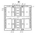
図1には、積層されたLSIの一形態が示される。積層されたLSIの積層断面が図示されている。本形態においては、パッケージ基板100の上層に外部通信LSI130が積層され、その上層に演算器を搭載したプロセッサLSI120〜121が積層され、またその上層にデータの記憶を行うメモリLSI110〜111が積層される。外部通信LSIは、この積層LSI外のシステム基板上の部品との間で通信周波数1GHzを超える高速な有線通信を行う回路を備え、積層LSI外部との高速通信はこの外部通信LSIを介して行う。 FIG. 1 shows one form of stacked LSIs. A laminated cross section of the laminated LSI is shown. In this embodiment, the
外部通信LSIは回路・配線面をパッケージ基板側に向けたフリップ接続をされる。プロセッサLSIは、CPUなど汎用のプロセッサや、グラフィックス・アクセラレータなどの専用プロセッサや、加算器や乗算器などの演算回路を多数ならべてその間をスイッチ回路で接続した動的再構成可能プロセッサや、FPGAを搭載するLSIが該当する。メモリLSIは、DRAMや、SRAM、フラッシュメモリ、磁性体メモリなどのメモリセルアレイからなる記憶装置を搭載するLSIが該当する。 The external communication LSI is flip-connected with the circuit / wiring surface facing the package substrate. The processor LSI is a general-purpose processor such as a CPU, a dedicated processor such as a graphics accelerator, a dynamic reconfigurable processor in which a large number of arithmetic circuits such as adders and multipliers are connected by a switch circuit, and an FPGA. Applicable to LSIs with. The memory LSI corresponds to an LSI on which a storage device including a memory cell array such as DRAM, SRAM, flash memory, and magnetic memory is mounted.
このように、図1に記載の発明は、ひとつの半導体パッケージ内に、外部通信LSI、プロセッサLSIおよびメモリLSIをこの順序で積層し、これらのLSI間を貫通電極で接続することで、高速かつ大容量の通信を行うことを特徴とする。ここで、シリコン貫通電極とは、基板シリコンに穴をあけ、その穴に導電物質をつめたものであり、これにより積層されたLSI間を電気的に接続できる。 As described above, the invention described in FIG. 1 is configured such that an external communication LSI, a processor LSI, and a memory LSI are stacked in this order in a single semiconductor package, and these LSIs are connected by through electrodes, thereby achieving high speed and high speed. It is characterized by high-capacity communication. Here, the through silicon via is a hole formed in a substrate silicon and a conductive material is filled in the hole, whereby the stacked LSIs can be electrically connected.
ここで、積層の順序を上記のような順序にしたのは、以下に述べる理由からである。 Here, the reason why the stacking order is set as described above is as follows.
まずメモリLSIは、外部通信LSIやプロセッサLSIとは製造プロセスが異なる場合があり、また、それに伴い自社では製造が難しい場合がある。例えばDRAMの設計プロセスは、DRAMがキャパシタを有する構造のため、一般のLSI製造プロセスとは異なる。そこで、外部通信LSIやプロセッサLSIは自社で開発し、DRAM LSIを他社から購入する場合を考えると、メモリLSIを最上位に配置することによって組み立てやテストが比較的容易になり、パッケージの歩留まりが向上する。 First, a memory LSI may have a different manufacturing process from an external communication LSI or a processor LSI, and accordingly, it may be difficult to manufacture by itself. For example, the DRAM design process is different from a general LSI manufacturing process because the DRAM has a capacitor structure. Therefore, considering the case where external communication LSIs and processor LSIs are developed in-house and DRAM LSIs are purchased from other companies, assembly and testing becomes relatively easy by placing the memory LSIs at the highest level, which increases the package yield. improves.
またメモリLSIに、積層へ向けた多数の入出力端子が予め用意されている場合、最上位に配置すれば、メモリLSIに対して片面もしくは上面から下面にかけて電極を形成させる加工を施す必要がなく、積層パッケージの歩留まり向上、開発コストの削減が実現できる。 If a memory LSI has a large number of input / output terminals for stacking in advance, if it is placed at the top, there is no need to process the memory LSI to form electrodes from one side or from the top to the bottom. It is possible to improve the yield of stacked packages and reduce development costs.
次に、外部通信LSIは、高速通信を行うため分岐やつなぎ目の少ない伝送路を形成する必要がある。そこで、外部通信LSIを最下層に配置することで、パッケージ基板に直接接続することが可能となり、分岐やつなぎ目の少ない伝送路を形成することが容易となるため、高速通信をより効率的に行うことが可能となる。 Next, the external communication LSI needs to form a transmission path with few branches and joints in order to perform high-speed communication. Therefore, by placing the external communication LSI on the bottom layer, it is possible to connect directly to the package substrate, and it becomes easy to form a transmission path with few branches and joints, so high-speed communication is performed more efficiently. It becomes possible.
また、前述したように、外部通信LSIとプロセッサLSIは一般的な設計プロセスで製造することができる。これら外部通信LSIとプロセッサLSIを自社内で製造し積層した時点で、メモリLSIを積層する前での動作テストを実施することにより、積層失敗時の損失を低減できる。 As described above, the external communication LSI and the processor LSI can be manufactured by a general design process. When these external communication LSIs and processor LSIs are manufactured and stacked in-house, an operation test is performed before stacking the memory LSIs, thereby reducing loss when stacking fails.
以上の理由から、最上層にメモリLSIを配置し、最下層に外部通信LSIを配置し、その間にプロセッサLSIを配置する。そして、シリコン貫通電極140〜141を設けることで、各LSI間の通信を可能とする。図1においては、シリコン貫通電極140〜141は全てのLSIを貫通しているが、全てのLSIを貫通する必要はない。外部通信LSIは回路を配置される面を上向き(フェイス・アップ)に配置することで、シリコン貫通電極140〜141が外部通信LSIを貫通することは不要となる。また、メモリLSIは、回路を配置される面を下向き(フェイス・ダウン)に配置することで、シリコン貫通電極140〜141がメモリLSIを貫通することは不要となる。または、後述のインタポーザを用いることによっても、シリコン貫通電極140〜141がメモリLSIを貫通することは不要となる。よって、最低限の構成としては、シリコン貫通電極140〜141はプロセッサLSIのみを貫通する構成とすることで、SoC全体の通信を可能とする構成を実現できる。 For the above reasons, the memory LSI is arranged in the uppermost layer, the external communication LSI is arranged in the lowermost layer, and the processor LSI is arranged therebetween. By providing the silicon through
加えて、メモリLSIが特定のメモリである場合には、特に最上位にメモリLSIを配置することにより、メモリLSIの放熱性が向上する点が有効となる。例えば、メモリLSIがDRAMである場合は、DRAMは熱によってデータのリフレッシュ時間が短くなってしまうといった問題がある。あるいは、メモリLSIが相変化メモリである場合は、相変化素子は熱により記憶情報を書き込むため、熱による記憶情報のディスターブが問題となる場合がある。 In addition, when the memory LSI is a specific memory, it is effective to improve the heat dissipation of the memory LSI, particularly by arranging the memory LSI at the highest level. For example, when the memory LSI is a DRAM, there is a problem that the DRAM refreshes the data refresh time due to heat. Alternatively, when the memory LSI is a phase change memory, since the phase change element writes stored information by heat, disturbing the stored information by heat may be a problem.
このように熱によって動作性能に与える影響が大きなメモリを積層する場合、メモリLSIを一番上に積層し上面に放熱板を取り付けることによって、放熱効果を高めることが可能となる。これにより、前述の相変化メモリのようなメモリにおいては、記憶情報のディスターブが低減され信頼性が向上する。そして、DRAMにおいては、とりわけ放熱性の効果が顕著に現れる。すなわち、DRAMの場合はリフレッシュ回数を低減することが可能となり、通信性能及び電力性能の向上が実現できるという顕著な効果を有する。 In the case of stacking memories having a large influence on the operation performance due to heat in this way, it is possible to enhance the heat dissipation effect by stacking the memory LSI on the top and attaching a heat sink on the upper surface. Thereby, in a memory such as the above-described phase change memory, disturbance of stored information is reduced and reliability is improved. In DRAM, the effect of heat dissipation is particularly significant. That is, in the case of DRAM, it is possible to reduce the number of refreshes, and there is a remarkable effect that improvement in communication performance and power performance can be realized.
図1において、積層されたLSI間は、シリコン基板に垂直方向に穴をあけ、その穴に導電性の物質を挿入して配線を形成したシリコン貫通電極(140〜141、145〜146、150〜151、160〜161、190〜191)と、ボンディングワイヤ(170〜171、175〜176、180〜181、185〜186)により接続される。シリコン貫通電極145〜146、シリコン貫通電極190〜191は電源供給のためのシリコン貫通電極である。シリコン貫通電極145〜146はメモリLSIとプロセッサLSIと外部通信LSIへ共通の電源を供給するためのシリコン貫通電極であり、電源はパッケージ外部からパッケージ基板、外部通信LSI、シリコン貫通電極145〜146を介して、メモリLSIとプロセッサLSIの電源ラインに接続される。シリコン貫通電極190〜191はプロセッサLSIのみが必要とする電源を供給するためのシリコン貫通電極であり、電源はパッケージ外部からパッケージ基板、ボンディングワイヤ180〜181を介して、プロセッサLSIの電源ラインおよびシリコン貫通電極190〜191に接続される。この電源は貫通電極190〜191を介して外部通信LSIに供給されてもよい。また同様に、シリコン貫通電極160〜161はメモリLSIのみが必要とする電源を供給するためのシリコン貫通電極であり、電源はパッケージ外部からパッケージ基板、ボンディングワイヤ170〜171を介して、メモリLSIの電源ラインおよびシリコン貫通電極160〜161に接続される。すなわち、ワイヤボンディングとシリコン貫通電極を併用することでプロセッサLSIとメモリLSIの電源は、その下方及び上方から供給することが可能となり、上方に設けられたプロセッサLSIやメモリLSIに対しても安定した電源を供給することが可能となる。この点は特に、多数のLSIを積層する場合に顕著になる。 In FIG. 1, between stacked LSIs, holes are formed in a vertical direction in a silicon substrate, and a conductive material is inserted into the holes to form wirings (140 to 141, 145 to 146, 150 to 151, 160-161, 190-191) and bonding wires (170-171, 175-176, 180-181, 185-186). The through
ここで、メモリLSIとプロセッサLSIがシリコン貫通電極145〜146とは別にシリコン貫通電極160〜161およびシリコン貫通電極190〜191を有する理由は、電圧の異なる電源をそれぞれのLSIに供給するためである。異なる電圧を供給する経路は、異なる端子により構成される方が、動作が安定となる。例えば、プロセッサLSIに供給する電源電圧が最も低く、メモリLSIに供給する電源電圧がプロセッサLSIよりも高く、外部通信LSIに供給する電源電圧が更に大きい場合がある。このような場合、別経路を用意して各LSIに電源を供給するほうが、シリコン貫通電極145〜146等のその他の回路に不要な負荷がかからず、回路の誤動作を防止できる。 Here, the reason why the memory LSI and the processor LSI have the silicon through
次に本実施の形態における各LSIおよびパッケージ外部との通信の経路について記載する。プロセッサLSI間の通信は、シリコン貫通電極150〜151を介す。プロセッサLSIとメモリLSI間の通信は、シリコン貫通電極140〜141を介す。プロセッサLSIと外部通信LSI間の通信は、シリコン貫通電極140〜141と、ボンディングワイヤ185〜186と、パッケージ基板100内の配線を介す。プロセッサLSIとパッケージ外部との通信は、シリコン貫通電極140〜141と、ボンディングワイヤ185〜186と、パッケージ基板100内の配線と、システム基板101内の配線を介する。外部通信LSIとメモリLSI間の通信は、シリコン貫通電極シリコン貫通電極140〜141と、ボンディングワイヤ175〜176を介す。外部通信LSI130とパッケージ外部との通信は、パッケージ基板100内の配線と、システム基板101内の配線を介する。メモリLSIとパッケージ外部との通信は、シリコン貫通電極140〜141と、外部通信LSI130と、パッケージ基板100内の配線と、システム基板101内の配線を介する。また、ここでいう通信とは、狭義の通信ではなく、リセット信号や、エンディアン信号や、動作周波数や端子設定などの初期値信号や、LSIの識別子信号なども含め電源以外のすべての情報の入出力をさす。 Next, communication paths between each LSI and the outside of the package in this embodiment will be described. Communication between the processor LSIs passes through the through silicon vias 150-151. Communication between the processor LSI and the memory LSI is performed through the through silicon vias 140-141. Communication between the processor LSI and the external communication LSI is performed through the silicon through
通信のための経路としては、プロセッサLSI、メモリLSI及び外部通信LSIのいずれも貫通するシリコン貫通電極140〜141と、プロセッサLSI同士を接続するシリコン貫通電極150〜151が設けられている。さらに、データ通信用のボンディングワイヤ175〜176によってメモリLSIとパッケージ基板が接続されている。同様に、ボンディングワイヤ185〜186によって、プロセッサLSIとパッケージ基板が接続されている。 As communication paths, through
このシステムの典型的な動作は、外部通信LSI130がパッケージ外部から画像や通信パケットなど処理対象データを積層されたメモリLSI110〜111に読み込み、このデータに対してプロセッサLSI120〜121が何らかの演算処理を行う。そして、その結果をメモリLSI110〜111に格納し、その結果を外部通信LSI130がメモリLSI110〜111から外のストレージやネットワークに出力するというものになる。本発明の積層LSIは、外部通信LSI、プロセッサLSI、メモリLSIが順に積層されているため、積層パッケージ上面に放熱板を取り付けるなどしてメモリLSIの放熱性能をより高めることができ、積層パッケージ内部のメモリLSIにデータを保持する時間が長い用途で積層LSIを用いる場合に、積層LSI全体の低消費電力化を実現できる。 The typical operation of this system is that the
図1においては、全体を接続するシリコン貫通電極140〜141の他に、シリコン貫通電極150〜151というシリコン貫通電極を設けている。しかし、シリコン貫通電極150〜151を用いて行っているプロセッサLSI間の通信も、共通のシリコン貫通電極140〜141を用いて行うことも可能である。この場合は、プロセッサLSIのシリコン貫通電極の数を削減でき、プロセッサLSIの面積の点で有利である。 In FIG. 1, in addition to the silicon through
一方、プロセッサLSI間のみを接続するシリコン貫通電極150〜151を設けることで、プロセッサLSI間に要求される高速通信を実現することが可能となる。 On the other hand, by providing the through silicon vias 150 to 151 that connect only the processor LSIs, it is possible to realize the high-speed communication required between the processor LSIs.
本実施例では、積層されたLSIの一部を接続するシリコン貫通電極150〜151は、プロセッサLSI間のみを接続するものとして記載されているが、一部のLSI間を接続するシリコン貫通電極とすることも可能である。例えば、積層されたLSIの一部を接続するシリコン貫通電極として、他のLSI(例えば、プロセッサLSIとメモリLSI)を接続する方式を採ることもできる。このとき、どのLSIを貫通する場合においても、接続されたLSI間において高速通信が可能となる。 In this embodiment, the silicon through electrodes 150 to 151 that connect a part of the stacked LSIs are described as connecting only between the processor LSIs. It is also possible to do. For example, a method of connecting another LSI (for example, a processor LSI and a memory LSI) can be adopted as a through silicon via that connects a part of the stacked LSIs. At this time, high-speed communication is possible between the connected LSIs regardless of which LSI is penetrated.
また、図1の実施の形態においては積層されたLSI間は直接接続されているが、メモリLSIとプロセッサLSI間、および、プロセッサLSIと外部通信LSI間に端子位置調整用の配線を持つインタポーザ層が挿入される場合もある。インタポーザにより、メモリLSIのシリコン貫通電極の位置と、プロセッサLSIのシリコン貫通電極の位置が一致しない場合の位置合わせを容易にすることができる。また同じ目的で、再配線層を用いることもできる。 In the embodiment shown in FIG. 1, the stacked LSIs are directly connected, but the interposer layer has wiring for adjusting terminal positions between the memory LSI and the processor LSI and between the processor LSI and the external communication LSI. May be inserted. The interposer can facilitate alignment when the position of the silicon through electrode of the memory LSI and the position of the silicon through electrode of the processor LSI do not match. A rewiring layer can also be used for the same purpose.
図2は、メモリLSIの一実施の形態を示す。記憶部200〜203はメモリアレイを含むブロックであり、シリコン貫通電極群220〜223はプロセッサLSIおよび外部通信LSIと通信するためのシリコン貫通電極信号群であり、図1のシリコン貫通電極140〜141に相当する。通信制御ブロック210〜213はシリコン貫通電極群220〜223を用いて通信するためのブロックであり、シリコン貫通電極群220〜223と通信制御ブロック210〜213とを併せて他のLSIとの入出力ポートを構成する。電極250はボンディングワイヤ(図1の170〜171)で電源を供給するための電極であり、電極250から供給された電源は供給されたメモリLSIの電源として、さらに、シリコン貫通電極160〜161に接続され下層のメモリLSIにも電源供給される。電極260〜267には図1のボンディングワイヤ175〜176が接続され、エンディアン信号や、LSIの識別子信号、LSIの機能を指定するための信号などに用いられる。 FIG. 2 shows an embodiment of a memory LSI. The
メモリLSI110〜111は、プロセッサLSI120〜121および外部通信LSI130が出力したデータの読出し/書き込み要求を、シリコン貫通電極群220〜223を介して受信し、その要求に従って記憶部200〜203への読み出し/書き込み処理を行い、読み出しの場合は読み出したデータを含む返答情報をシリコン貫通電極群220〜223に出力する。読出し/書き込み要求は、LSI間の同期をとるための情報、積層された複数のメモリLSIからひとつを選択するためのLSI選択情報、読出し/書き込みを示すコマンド情報、アドレス情報、処理識別子、書き込み時には書き込みデータを含む。返答情報は、LSI間の同期をとるための情報、読出しデータ、処理識別子を含む。処理識別子は、メモリLSIへの読出し/書き込み要求に含まれる情報であり、メモリLSIは返答情報にこの処理識別子を含める。読出し/書き込み要求の発行元であるプロセッサLSI120〜121や外部通信LSI130は、処理識別子を見て自分が発行した要求に対応する返答情報を選別する。多数の積層されたLSIがメモリLSI110〜111に対して要求を行う場合、他のLSIからの要求もシリコン貫通電極上に出力されるため、処理識別子が必要となる。ここで、処理識別子とは、読み出し又は書き込み要求の際のデータの送信先及び送信元のデータを指す。この処理識別子を付加することによって、同種のLSIを積層してもLSIの区別が可能となるため、同種のLSIを積層することが可能となり、スケーラビリティーを向上することができる。また、要求信号には、後述の調停要求の信号も付加される。 The memory LSIs 110 to 111 receive data read / write requests output from the
このように、処理識別子を付加した要求を行うことによって、ある共通のシリコン貫通電極を複数のLSIで使用することが可能となる。 As described above, a common through silicon via can be used in a plurality of LSIs by making a request with a processing identifier added.
図3は、プロセッサLSIの一実施の形態を示す。プロセッシングユニット300〜307は演算を行うブロックであり、DMAC350〜351はデータ転送ブロックであり、周辺回路ブロック355〜356は割込み制御やクロック制御やタイマなどを含むブロックであり、シリコン貫通電極群220〜223 はメモリLSIや外部通信LSIと通信するためのシリコン貫通電極信号群であり、通信制御ブロック370〜373はLSIがシリコン貫通電極群220〜223を用いて行う通信を制御するためのブロックであり、シリコン貫通電極群220〜223と通信制御ブロック370〜371とを併せて他のLSIとの入出力ポートを構成する。シリコン貫通電極群380〜383 は他のプロセッサLSIとの通信するためのシリコン貫通電極信号群であり、制御ブロック385〜388はシリコン貫通電極群380〜383を用いて通信するためのブロックである。テストブロック360〜361はプロセッサLSIと外部通信LSIの動作テストを行うブロックであり、制御ブロック365〜366はボンディングワイヤを介して外部通信LSIへの通信および積層LSI外部への低速通信するための制御ブロックであり、オンチップインタコネクト390〜391はオンチップのブロック間を接続するブロックであり、ブリッジ回路395はオンチップインタコネクト390〜391間を接続するブリッジ回路であり、シリコン貫通電極145〜146とシリコン貫通電極190〜191は図1で示した電源供給用のシリコン貫通電極であり、電極340はボンディングワイヤ(図1の180〜181)で電源を供給するための電極であり、電極340から供給された電源は供給されたプロセッサLSIの電源として、さらに、シリコン貫通電極190〜191に接続され下層のプロセッサLSIにも電源供給される。電極310〜317には図1のボンディングワイヤ185〜186が接続され、エンディアン信号や、LSIの識別子信号、LSIの機能を指定するためなどに用いられる。 FIG. 3 shows an embodiment of the processor LSI. The
プロセッシングユニット300〜307やDMAC350〜351などからメモリLSI内の記憶領域へのデータの読出し/書き込みが発生すると、その要求がオンチップインタコネクト390〜391を介して通信制御ブロック370〜373に伝達し、通信制御ブロック370〜371はその要求に基づきシリコン貫通電極群220〜223を介してメモリLSI110〜111にデータの読出し/書き込み要求を出力する。このアクセスに対するメモリLSI110〜111からの返答データを、シリコン貫通電極群220〜223を介して通信制御ブロック370〜371が受信し、通信制御ブロック370〜371はその情報を、メモリLSI110〜111への要求をおこなったプロセッシングユニット300〜307やDMAC350〜351にオンチップインタコネクト390〜391を介して出力する。シリコン貫通電極群380〜383は、図1におけるシリコン貫通電極150〜151を示しており、プロセッサLSI間の通信に用いられる。シリコン貫通電極群380〜383には、あるプロセッサLSIのプロセッシングユニット300〜307やDMAC350〜351などから別のプロセッサLSIへの読出し/書き込み要求信号、この読出し/書き込みに対する返答のための信号、プロセッサLSI間の割り込み関連信号、プロセッサLSI間のメモリコヒーレンスをとるための信号、プロセッサLSI間でタイミング同期を取るための信号、プロセッサLSIのソフトウェアデバッグをサポートする信号などが含まれる。ここで、インタフェースの配置箇所をLSI間で同一にすることで、積層した際に鉛直方向のみの通信を行うことが可能となる。すると、水平又は斜め方向に通信する場合と比較して、それぞれのLSIにおける面内の通信が不要となり、面積コストを削減することができる。 When data is read from or written to the storage area in the memory LSI from the
図4は、外部通信LSI130の一実施の形態を示す。インタフェース回路ブロック400〜401は3D積層パッケージ外部の部品との間で高速な通信を行うブロックであり、制御ブロック410〜411はインタフェース回路ブロック400〜401を制御するためのブロックであり、コントローラマイコン420〜421は制御ブロック410〜411を制御するための小型のコントローラマイコンであり、テストブロック430〜431はプロセッサLSIと外部通信LSIの動作テストを行うブロックであり、シリコン貫通電極群220〜223 はメモリLSIとの通信するためのシリコン貫通電極信号群であり、通信制御ブロック460〜463はシリコン貫通電極群220〜223を用いて通信するためのブロックであり、オンチップインタコネクト450〜451はオンチップのブロック間を接続するブロックである。制御ブロック410〜411は、内蔵レジスタに指定されたアドレス領域間でのデータ転送を行うDMAC440〜441を含む。また、コントローラマイコン420〜421は、プロセッサLSIとの通信を行うプログラムや、制御ブロック410〜411のレジスタの設定を行うプログラムなど、積層された他のLSIやパッケージ外部との通信にかかわる処理を実行する。 FIG. 4 shows an embodiment of the
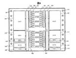
図5は、積層されたLSI同士の位置関係を示した図である。図のように、下から外部通信LSI、プロセッサLSI、メモリLSIが積層され、図において各LSIの中央部に存在するシリコン貫通電極によって、電源の共有と信号の伝達が行われる。それぞれのメモリLSIは4つの入出力ポートを持ち、4つのポートそれぞれにシリコン貫通電極信号群シリコン貫通電極群220〜223が接続されている。このシリコン貫通電極に対してプロセッサLSIと外部通信LSIが接続され、プロセッサLSIと外部通信LSIは共有するシリコン貫通電極群220〜223を時分割で使用し、メモリLSIにアクセスする。各シリコン貫通電極群220〜223は複数のLSIで共有されるため同時にメモリにアクセスすることはできない。そのため、プロセッサLSI120〜121、外部通信LSI130からの各シリコン貫通電極群220〜223の使用要求を調停し、プロセッサLSI120〜121、外部通信LSI130のうちのいずれかひとつに、シリコン貫通電極群220〜223の使用権をあたえる調停機能を、シリコン貫通電極群220〜223毎にひとつ設ける。この調停機能は、シリコン貫通電極ごとに実施する調停機能ブロックが存在するLSIを変更してもよく、例えば、あるシリコン貫通電極の調停機能はプロセッサLSI120の通信制御ブロックが有し、異なるシリコン貫通電極の調停機能は外部通信LSIの通信制御ブロックが有してもよい。ここで、調停機能を特定のLSIに持たせる方法については、後述する。 FIG. 5 is a diagram showing the positional relationship between the stacked LSIs. As shown in the figure, an external communication LSI, a processor LSI, and a memory LSI are stacked from the bottom, and power supply sharing and signal transmission are performed by a through silicon via that exists in the center of each LSI in the figure. Each memory LSI has four input / output ports, and a through silicon via
あるシリコン貫通電極を介して通信を実施したいプロセッサLSIもしくは外部通信LSIがある場合、対象となるシリコン貫通電極を調停するブロックをもつLSIに対して使用要求を発行し、使用を許可されたLSIがシリコン貫通電極を使用してメモリLSIへのアクセスや他のLSIへのアクセスを行う。 When there is a processor LSI or external communication LSI that wants to communicate via a silicon through electrode, a use request is issued to the LSI that has a block that arbitrates the target silicon through electrode, and the LSI that is permitted to use is issued. Access to the memory LSI and other LSIs using through silicon vias.
メモリLSIとプロセッサLSI間、および、プロセッサLSIと外部通信LSI間の接続を上記のように行う主な理由は、積層枚数を変更しても同様の接続方式で対応することが可能であるため、積層枚数に対するスケーラビリティーが高いことがある。 The main reason for the connection between the memory LSI and the processor LSI and between the processor LSI and the external communication LSI as described above is that it can be handled with the same connection method even if the number of stacked layers is changed. Scalability with respect to the number of stacked layers may be high.
一方、シリコン貫通電極群380〜383は、プロセッサLSI間の通信を行うための信号である。別のプロセッサLSI内のオンチップメモリや機能回路へのアクセスなどにはこのシリコン貫通電極を用いる。例えば、プロセッサLSI120内のプロセッシングユニット300が、プロセッサLSI121のプロセッシングユニット301内のメモリ領域への読み出し/書き込みを行いたい時、プロセッサLSI120内のプロセッシングユニット300は接続されるオンチップインタコネクト390に読み出し/書き込み要求を発生する。この要求にはプロセッサLSI121のプロセッシングユニット301内のアクセス対象となる部分を指す要求先アドレス情報、返信をするための要求元アドレス情報、コマンドなどが含まれる。要求を受けたオンチップインタコネクト390はその要求先アドレス情報をデコードし、プロセッサLSI120内の制御ブロック385にプロセッサLSI121への読み出し/書き込み要求を発行する。この制御ブロック385はシリコン貫通電極群380に要求を出力し、プロセッサLSI121内のシリコン貫通電極群380を介してプロセッサLSI121内の制御ブロック385がこの要求を受け取る。この制御ブロック385はプロセッサLSI121内のオンチップインタコネクト390にこの要求を出力し、プロセッサLSI121内のオンチップインタコネクト390は要求先アドレスに基づきプロセッサLSI121内のプロセッシングユニット301に要求を送信する。要求を処理したプロセッサLSI121内のプロセッシングユニット301は返答を要求元アドレスとともに返信する。返信された情報は要求元アドレスに従って、プロセッサLSI120内のプロセッシングユニット300に返信される。 On the other hand, the through silicon via
図6は、プロセッサLSI120〜121内の通信制御ブロック370〜373およびシリコン貫通電極群220〜223について示した図である。この通信制御ブロック370〜373は、接続されるシリコン貫通電極群220〜223の使用権の調停を行う。図1や図5に示すように同一のマスクで製造したプロセッサLSIを複数積層するため、各通信制御ブロック370〜373が調整を行うかどうかを指定する必要があり、調停機能を有する通信制御ブロック370〜373を示すための指定信号600によりこれを指定する。指定信号600信号は、1ビットであることも、複数ビットであることもある。指定信号600に値を与える方法の一つとしては、ヒューズ回路を用いる方法がある。このヒューズを用いる方法では、積層組み立て時に、指定信号600が所望の値となるよう、電気あるいはレーザーなどで負荷を与えてヒューズを切断する。また、指定信号600を与える別の方法としては、LSI内に不揮発メモリデバイスを集積し、この不揮発メモリの出力を指定信号600に接続し、積層組み立て時にこの不揮発メモリデバイスに指定信号600の値を書きこむ方法がある。また、指定信号600を与える別の方法としては、この指定信号600をLSI外部端子として引き出しておき、積層組み立て時にワイヤボンディングなどを用いてこの外部端子に0/1信号を接続する方法がある。また、指定信号600を与える別の方法としては、指定信号600信号をプロセッシングユニット300〜307から書き込み可能な記憶素子の出力に接続し、起動後にプロセッシングユニット300〜307によりこの記憶素子に指定信号600値を書き込む方法がある。ここで、指定信号600を特別に設けずに、特定のLSIを特別な構成にして調停機能を持たせることも可能ではあるが、そのためには、調停機能を持たせるLSIを特別のマスクを用いて製造する必要があり、製造コストが増大してしまう。それに対し、本実施例のように指定信号600によって通信制御ブロック370〜373に調停機能を持たせる構成とすることで、調停機能を持たせるLSIを特別な構成にする必要がなくなり、マスクの作成コストを抑えることができる。 FIG. 6 is a diagram showing the communication control blocks 370 to 373 and the through silicon via
ここで調停機能をプロセッサLSI120に持たせるとすると、制御ブロック610はプロセッサLSI121からのシリコン貫通電極群220〜223使用要求信号(信号620)、自プロセッサLSI(プロセッサLSI120)のプロセッシングユニット300〜307やDMAC350〜351など回路ブロックからのシリコン貫通電極群220〜223使用要求信号(信号621)、外部通信LSI130からのシリコン貫通電極群220〜223使用要求信号(信号622)を受け、シリコン貫通電極群220〜223の使用権の調停を行う。より具体的には、信号620は、プロセッサLSI121から出力され、シリコン貫通電極220〜223を介して、制御ブロック610に伝達される。信号621は、プロセッサLSI120内の回路ブロックから出力され、内部のオンチップインタコネクト390〜391を介して、制御ブロック610に伝達される。信号622は、外部通信LSI130から出力され、シリコン貫通電極群220〜223を介して、制御ブロック610に伝達される。制御ブロック610は、調停の結果、使用権を与える回路に使用許可信号をアサートする。信号630はプロセッサLSI121へのシリコン貫通電極群220〜223使用許可信号であり、信号631はプロセッサLSI120内部のプロセッシングユニット300〜307やDMAC350〜351などへのシリコン貫通電極群220〜223使用許可信号であり、信号632は外部通信LSI130へのシリコン貫通電極群220〜223使用要求信号である。信号630は、シリコン貫通電極220〜223を介して、プロセッサLSI121に伝達される。信号631は、内部のオンチップインタコネクト390〜391を介して、使用権を要求した回路ブロックに伝達される。信号632は、シリコン貫通電極220〜223を介して、外部通信LSIに出力される。 Here, assuming that the
シリコン貫通電極640〜641はメモリへのアクセス要求を行うためのシリコン貫通電極である。シリコン貫通電極群220〜223使用許可を受けたLSIの通信制御ブロック370〜373がこのシリコン貫通電極640〜641にメモリアクセス要求を出力する。シリコン貫通電極640〜641を用いて、LSI間の同期をとるための情報、積層された複数のメモリLSIからひとつを選択するためのLSI選択情報、読出し/書き込みを示すコマンド情報、アドレス情報、処理識別子、書き込みデータなどをメモリに送信する。 The through
シリコン貫通電極650〜651はメモリが読み出しデータなどを返すためのシリコン貫通電極である。要求を出した通信制御ブロック370〜371はメモリから出力された読出しデータ、処理識別子、タイミング同期を取るための信号などを受信する。 The through
また、図6内のインタフェース回路660はオンチップインタコネクト390〜391との接続回路であり、データ変換回路670はオンチップインタコネクト390〜391からの読み出し/書き込み要求をシリコン貫通電極640〜641への出力形式に変換し制御ブロック610に指示されるタイミングで出力する回路であり、データ変換回路671はシリコン貫通電極650〜651を介して得られたデータのうち必要なデータを選択し形式変換を行い、インタフェース回路660へ出力する回路である。 6 is a connection circuit with the on-
信号制御ブロック680、信号制御ブロック681、信号制御ブロック682はシリコン貫通電極への信号送信、または、シリコン貫通電極からの信号受信を行う回路ブロックである。信号制御ブロック680は、送受信双方向の回路ブロックであり、シリコン貫通電極群220〜223の使用要求および使用許可信号に用いられる。また、制御信号690および制御信号691はシリコン貫通電極との通信を制御する信号である。 The
また、積層されるプロセッサLSIは、プロセッサLSIなど同じ構成を持つLSI同士を識別する信号を備える。例えば、プロセッサLSIに搭載されるプロセッシングユニット300〜307はこの信号からの情報により、自身が何番目のプロセッシングユニット300〜307であるかを知ることができる。この情報をプロセッシングユニット300〜307上で動作するプログラムから利用することで、プロセッシングユニット300〜307毎に動作を変えることができる。この識別信号値は、指定信号600と同様の手法により、製造後にLSI毎に与えられる。 The stacked processor LSIs include signals for identifying LSIs having the same configuration, such as processor LSIs. For example, the
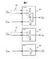
図7に信号制御ブロック680、信号制御ブロック681、信号制御ブロック682、それぞれの回路ブロックの回路構成を示す。信号制御ブロック681は、シリコン貫通電極に信号を出力するための回路ブロックである。本回路は、シリコン貫通電極への出力端子と、出力するデータの入力端子と、信号を出力するか、入力信号に依らずフローティング状態(あるいは弱い信号出力)とするかを指定するための制御入力端子をもつ。ここで、データの入力端子と制御入力端子への入力は図6に記載する制御ブロック670が出力し、このうちの制御入力端子には信号691が接続される。この信号691はシリコン貫通電極群220〜223の使用権が得られたブロックがデータを出力する期間のみアサートされ、この期間回路ブロックは活性化し、信号制御ブロック681からシリコン貫通電極群220〜223にデータが出力される。その他の期間はフローティングされ非活性状態となり、入力の値に依らずシリコン貫通電極群220〜223への出力を高インピーダンス状態とし、シリコン貫通電極群220〜223の使用権を他の回路に開放する。この構成により、他のLSIが通信を行う場合の当該LSIによる影響を無くすことが可能であるため、複数のLSIを同一の貫通電極を介してデータ通信することが可能となる。この構成及び効果は、下記の信号制御ブロック682でも同様である。 FIG. 7 shows a circuit configuration of each of the
信号制御ブロック682は、シリコン貫通電極からのデータを受信するための回路である。 The
信号制御ブロック680は、図6の実施の形態においてシリコン貫通電極群220〜223の使用要求および使用許可信号に用いられる回路である。信号制御ブロック680は、シリコン貫通電極からの入力もシリコン貫通電極への出力も可能な回路構成をとる。接続される通信制御ブロック370〜373がシリコン貫通電極群220〜223の調停機能を担うかどうかで入力と出力が切り替わる。本例では、調停を行う場合について記載する。この時、信号620、信号622を介して他のLSIからシリコン貫通電極群220〜223の使用要求を受け、シリコン貫通電極群220〜223の使用許可を信号630および信号632を介して送信する。そのため、信号制御ブロック680は、信号620と信号622に対してはシリコン貫通電極群220〜223からの入力を受けるように指定され、信号630と信号632に対してはシリコン貫通電極群220〜223に出力を行うよう指定される。また、この信号制御ブロック680は、シリコン貫通電極への入出力端子と、図6における制御ブロック610からの入力端子と、信号を出力するかフローティング状態(あるいは弱い信号出力)とするかを指定するための制御入力端子をもつ。この制御入力端子への入力は、図6に記載する制御ブロック610が出力する信号690が接続される。この信号690は、対応する信号制御ブロック680が送信用であり、かつ、シリコン貫通電極群220〜223の使用権が得られデータを出力する期間のみアサートされる。すなわち、信号690がアサートされた期間に信号制御ブロック680から信号が出力される。信号制御ブロック680がシリコン貫通電極からの信号を受信するか、シリコン貫通電極へ信号を送信するかは、図6の指定信号600の値によって決まる。 The
図6、図7は、プロセッサLSI120およびプロセッサLSI121両方において同様の構成となる。 6 and 7 have the same configuration in both the
図8では、メモリLSI内のメモリ制御ブロック210〜213およびシリコン貫通電極群220〜223の部分について示す。インタフェース回路800は記憶部200〜203との接続回路であり、データ変換回路801はシリコン貫通電極群220〜223からの読み出し/書き込み要求を記憶部200〜203への出力形式に変換し、記憶部200〜203へ出力する回路であり、データ変換回路802は記憶部200〜203からの読み出しデータに付随する情報を合せて形式変換し信号制御ブロック820に出力する回路である。メモリへの読出し/書き込み要求が接続されるシリコン貫通電極640〜641には信号制御ブロック810が接続され、メモリからの返答を返すシリコン貫通電極650〜651には信号制御ブロック820が接続される。信号制御ブロック820に接続される制御信号830は、シリコン貫通電極群220〜223にデータを出力する期間のみアサートされ、この期間に信号制御ブロック681からシリコン貫通電極に対してデータが出力される。その他の期間はフローティング状態となる。 FIG. 8 shows the memory control blocks 210 to 213 and the through silicon via
図9では、外部通信LSI130内の通信制御ブロック460〜463およびシリコン貫通電極群220〜223について示す。シリコン貫通電極622〜623はメモリへのアクセス要求を行うためのシリコン貫通電極である。この外部通信LSIの通信制御ブロック460〜463は、シリコン貫通電極群220〜223内のシリコン貫通電極640〜641および650〜651の使用調停を行うプロセッサLSIの通信制御ブロック370〜373に対して、信号622を介してシリコン貫通電極640〜641使用要求を出力し、信号632を介してシリコン貫通電極640〜641の使用許可を得る。この外部通信LSIの通信制御ブロック460〜461は、使用許可が得られた場合に、シリコン貫通電極640〜641を介して、LSI間の同期をとるための情報、積層された複数のメモリLSIからひとつを選択するためのLSI選択情報、読出し/書き込みを示すコマンド情報、アドレス情報、処理識別子、書き込みデータなどを含むメモリへのアクセス要求を行う。 FIG. 9 shows communication control blocks 460 to 463 and through silicon via
シリコン貫通電極650〜651はメモリが読み出しデータなどの返答を返すためのシリコン貫通電極である。外部通信LSIの通信制御ブロック460〜463は、メモリから出力された読出しデータ、処理識別子、タイミング同期を取るための信号などをシリコン貫通電極650〜651を介して受信する。 The through
また、図9内の、インタフェース回路900はオンチップインタコネクト450〜451との接続回路であり、データ変換回路901はオンチップインタコネクト450〜451からの読み出し/書き込み要求をシリコン貫通電極640〜641への出力形式に変換し制御ブロック960に指示されるタイミングで出力する回路であり、データ変換回路902はシリコン貫通電極650〜651を介して得られたデータのうち必要なデータを選択し形式変換を行い、インタフェース回路900へ出力する回路である。 9, the
図10に、最上位層に積層するメモリLSIに対し、貫通電極を形成せずに積層する場合の実施例を示す。図に示すようにメモリLSI1000を外部から購入した場合、入出力端子としてボールなどの金属端子が用意されている。これを外部通信LSIやプロセッサLSIと積層し、接続するためにインタポーザ1010を挿入する。これにより、サイズや入出力端子の位置の異なるメモリLSIとプロセッサLSIの配線を接続することが可能となり、積層するメモリLSIの自由度が向上する。また更に、インタポーザ1010に放熱性の優れた材料ならびに構造を用いることにより、メモリLSIの放熱性を向上させることができ、パッケージ内部のメモリLSIにデータを保持する時間が長い用途で積層LSIを用いる場合に低消費電力化の効果が大きい。また、前述したように、最上位層のメモリLSIの上に放熱板を搭載することにより、放熱性能を向上させ、同様の効果が得られることは言うまでもない。 FIG. 10 shows an embodiment in which the memory LSI stacked on the uppermost layer is stacked without forming a through electrode. As shown in the figure, when the
この実施例を別の観点から見ると、外部通信LSI及びプロセッサLSIの上方にインタポーザを設けることにより、インタポーザの上方の自由度を確保する実施例と捉えることができる。インタポーザの上層は、特にメモリLSIとすることで、設計の自由度等の面から好適である。とりわけ、熱の影響が大きいDRAM、相変化メモリ等の場合に有効である。 From another point of view, this embodiment can be regarded as an embodiment in which the interposer is provided above the external communication LSI and the processor LSI to ensure the degree of freedom above the interposer. The upper layer of the interposer is particularly a memory LSI, which is preferable in terms of design freedom and the like. In particular, it is effective in the case of DRAM, phase change memory, etc., which are greatly affected by heat.
図11にインタポーザ1010の一実施例を示す。インタポーザ1010は、メモリLSI1000とプロセッサLSI120の間に積層され、メモリLSI1000とプロセッサLSI120の間を配線で接続するために設けられる。また、別の観点から捉えると、インタポーザはその上方の面にメモリLSI1000を接続するための接続端子を配置するために設けられる。この例ではメモリLSIとして一般的に規格化されたDRAMを積層する場合を例として説明する。プロセッサLSI120もしくは外部通信LSIに搭載されたDRAMコントローラ1140からメモリLSIへのアクセスを行う場合、2次元配線の場合は基板上で抵抗や反射を考慮した接続がなされる。ただし積層する場合はDRAMコントローラとメモリLSIの距離を始めとした物理パラメータが大きく異なる。そこで、インタポーザ1010内の貫通電極1120および1130、配線抵抗1100、電源1110を回路によって構成し、これらによって必要な物理パラメータを形成することにより、規格化されたメモリLSIとの接続も可能とすることができる。インタポーザはトランジスタゲート幅の大きな半導体プロセスで製造されてもよく、この場合は微細な半導体プロセスを用いるよりもコストが有利となる。また、半導体プロセスで製造される必要はなく、パッケージ基板やシステム基板といったもので製造されてもよい。また、インタポーザは製造後に配線構造を変更することができるFPGAなどによって構成されてもよい。幾つかの配線パラメータを切替えられる構成としておくことで、上面に積層するメモリLSIの自由度を向上されることが可能となる。 FIG. 11 shows an embodiment of the
また、このインタポーザは単に配線の接続と放熱のみを行う構成であっても良く、上述のメモリLSI1000とプロセッサLSI120の間を配線で接続するための機能と放熱性の機能の両方を実現するために設けることもできる。とりわけ、メモリLSI1000の面積が図10のようにプロセッサLSI120よりも小さい場合は、インタポーザの上面から放熱を行うことが可能となり、プロセッサLSI120の放熱をより効率的に行うことも可能となる。 In addition, this interposer may be configured to simply connect wiring and dissipate heat, in order to realize both the function for connecting the
このインタポーザにより、メモリLSIに貫通電極を形成することなく、積層パッケージを製造することが可能となり、開発コストを低くすることが可能となる。 With this interposer, a stacked package can be manufactured without forming a through electrode in the memory LSI, and the development cost can be reduced.
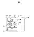
図12はテストブロック360〜361および430〜431を示す図である。プロセッサLSIおよび外部通信LSIに搭載され、メモリLSIを積層する前に、プロセッサLSIと外部通信LSIの動作テストを行うために使用する。図に示すようにテストブロック360はオンチップインタコネクト390に接続され、他の積層LSIとの通信を行い、データの送信と受信を行う。制御部1200は書き込み部1210に対してアドレスやデータなどを送信することにより、書き込み部1210は記憶部1230に対してデータを保存する。また、制御部1200は読出し部1220に対してアドレスや制御信号を送信することにより、読出し部は記憶部1230からデータを読出し制御部へ送信する。また制御部はオンチップインタコネクトを通じて得た受信データと記憶部1230内に格納されているデータの一致性を比較する機能を持ち、これによって通信制御のテストを行うことができる。より詳細には、本テストブロック中もしくは図6に示す貫通電極制御ブロックに、他LSIとの通信ディレイなどを測定する回路を設け、通信性能のテストを行ってもよい。このテストは、制御部1200内のROM1250に格納されたテストプログラムを用いて実行させてもよく、また、オンチップインタコネクト390を介してマイクロコントローラ420からの制御をレジスタ1240で受けて実行されてもよい。更に、通信テストの送信データや期待値は制御部1200内のROM1250に格納されていてもよい。 FIG. 12 is a diagram
これにより、メモリLSIを積層する前の段階でプロセッサLSIと外部通信LSIの積層テストを実施することが容易となる。 This makes it easy to perform a stacking test between the processor LSI and the external communication LSI before the memory LSI is stacked.
図10から図12に記載の発明を、半導体装置の製造方法の観点から捉えると、パッケージ基板上に外部通信LSIを積層する工程と、外部通信LSIの積層後外部通信LSIの上方にプロセッサLSIを積層する工程と、プロセッサLSIの積層後にインタポーザ層を積層する工程及び貫通電極を設ける工程を有することを特徴とする半導体装置の製造方法と考えることもできる。 The invention described in FIGS. 10 to 12 can be understood from the viewpoint of a manufacturing method of a semiconductor device. A process of stacking an external communication LSI on a package substrate, and a processor LSI above the external communication LSI after stacking the external communication LSI It can also be considered as a method of manufacturing a semiconductor device, characterized by having a step of stacking, a step of stacking an interposer layer after stacking of processor LSIs, and a step of providing a through electrode.
以上の工程は、同一のベンダが行う工程である。ここで、インタポーザ層を有することにより、その上方にメモリLSIを積層する工程は別のベンダが行うことが可能となり、メモリLSIを別ベンダから提供される場合に特に好適な製造方法となる。また、同一のベンダがメモリLSIの積層まで行う場合であっても、メモリLSIへシリコン貫通電極を貫通させる必要がなくなることによる歩留まり向上や開発コスト低減の効果もある。 The above steps are steps performed by the same vendor. Here, by having the interposer layer, the process of stacking the memory LSIs thereon can be performed by another vendor, which is a particularly preferable manufacturing method when the memory LSIs are provided from another vendor. Even when the same vendor performs the stacking of the memory LSIs, there is an effect of improving the yield and reducing the development cost by eliminating the need to penetrate the through silicon vias into the memory LSI.
さらに、上述の工程で製造する場合は、メモリLSIの積層を行う前に外部通信LSIとプロセッサLSIの間の動作テストを行うことが可能となるため、積層失敗時のリスクを低減した製造が可能となる。 Furthermore, when manufacturing with the above-mentioned process, it is possible to perform an operation test between the external communication LSI and the processor LSI before stacking the memory LSI, enabling manufacturing with reduced risk of stacking failure It becomes.
100:パッケージ基板
101:システム基板
110〜111:メモリLSI
120〜121:プロセッサLSI
130:外部通信LSI
140〜141、145〜146、150〜151、160〜161、190〜191:シリコン貫通電極
170〜171、175〜176、180〜181、185〜186:ボンディングワイヤ
200〜203:記憶部
220〜223:シリコン貫通電極群
210〜213:通信制御ブロック
250,260〜267:電極
300〜307:プロセッシングユニット
350〜351:DMAC
355〜356:周辺回路ブロック
360〜361:テストブロック
365〜366:制御ブロック
370〜373:通信制御ブロック
380〜383:シリコン貫通電極群
385〜388:制御ブロック
390〜391:オンチップインタコネクト
395:ブリッジ回路
340:電極
310〜317:電極
400〜401:インタフェース回路ブロック
410〜411:制御ブロック
420〜421:コントローラマイコン
430〜431:テストブロック
460〜463:通信制御ブロック
450〜451:オンチップインタコネクト
440〜441:DMAC
600:指定信号
610:制御ブロック
620〜622:シリコン貫通電極群220〜223使用要求信号
630〜632:シリコン貫通電極群220〜223使用許可信号
640〜641:シリコン貫通電極
650〜651:シリコン貫通電極
660:インタフェース回路
670:データ変換回路
680〜682:信号制御ブロック
690〜691:制御信号
800:インタフェース回路
801:データ変換回路
820:信号制御ブロック
810:信号制御ブロック
830:制御信号
900:インタフェース回路
901:データ変換回路
960:制御ブロック
902:データ変換回路
1000:メモリLSI
1010:インタポーザ
1140:DRAMコントローラ
1120および1130:貫通電極
1100:配線抵抗
1110:電源
1200:制御部
1210:書込み部
1230:記憶部
1220:読出し部
1250:ROM
1240:レジスタ100: Package substrate
101: System board
110 to 111: Memory LSI
120 to 121: Processor LSI
130: External communication LSI
140-141, 145-146, 150-151, 160-161, 190-191: Silicon through electrode
170-171, 175-176, 180-181, 185-186: Bonding wire
200 to 203: Storage unit
220 to 223: Silicon through electrode group
210 to 213: Communication control block
250, 260 to 267: Electrode
300 to 307: Processing unit
350-351: DMAC
355-356: Peripheral circuit block
360-361: Test block
365 to 366: Control block
370 to 373: Communication control block
380-383: Silicon through electrode group
385 to 388: Control block
390-391: On-chip interconnect
395: Bridge circuit
340: Electrode
310 to 317: Electrode
400 to 401: Interface circuit block
410-411: Control block
420 to 421: Controller microcomputer
430-431: Test block
460 to 463: Communication control block
450-451: On-chip interconnect
440-441: DMAC
600: Specified signal
610: Control block
620 to 622: Use request signal for through
630 to 632: Silicon through
640 to 641: Silicon through electrode
650 to 651: Silicon through electrode
660: Interface circuit
670: Data conversion circuit
680 to 682: Signal control block
690 to 691: Control signal
800: Interface circuit
801: Data conversion circuit
820: Signal control block
810: Signal control block
830: Control signal
900: Interface circuit
901: Data conversion circuit
960: Control block
902: Data conversion circuit
1000: Memory LSI
1010: Interposer
1140: DRAM controller
1120 and 1130: Through electrode
1100: Wiring resistance
1110: Power supply
1200: Control unit
1210: Writing part
1230: Memory unit
1220: Reading section
1250: ROM
1240: Register
Claims (19)
Translated fromJapanese前記パッケージ基板に接続され、前記パッケージ基板を介して通信を行うための通信回路を有する第1LSIと、
前記第1LSIの上方に設けられ、演算処理を行うための第2LSIと、
複数の第1ビット線及び複数の第1ワード線の交点に設けられた複数の第1メモリセルを具備し前記第2LSIの演算処理の結果を記憶するための第1記憶装置を有し、前記第2LSIの上方に設けられる第3LSIと、
前記第2LSIを貫通して設けられ、前記第1、第2及び第3LSIを互いに電気的に接続するための第1貫通電極とを有することを特徴とする半導体装置。A package substrate;
A first LSI connected to the package substrate and having a communication circuit for communicating via the package substrate;
A second LSI provided above the first LSI for performing arithmetic processing;
A first storage device comprising a plurality of first memory cells provided at intersections of the plurality of first bit lines and the plurality of first word lines, and storing a result of arithmetic processing of the second LSI; A third LSI provided above the second LSI;
A semiconductor device, comprising: a first through electrode provided through the second LSI and electrically connecting the first, second, and third LSIs to each other.
前記第2LSIと前記第3LSIの間に設けられ、前記第2LSIと前記第3LSIの間を配線で接続するためのインタポーザ層をさらに有することを特徴とする半導体装置。The semiconductor device according to claim 1,
A semiconductor device, further comprising an interposer layer provided between the second LSI and the third LSI for connecting the second LSI and the third LSI with a wiring.
前記第3LSIは、回路を配置される面の面積が前記第2LSIの回路が配置される面の面積と異なる大きさのLSIであることを特徴とする半導体装置。The semiconductor device according to claim 2,
The third LSI is a semiconductor device characterized in that an area of a surface on which a circuit is arranged is different from an area of a surface on which the circuit of the second LSI is arranged.
前記第3LSIは、接続端子の位置が第2LSIの接続端子の位置と異なるLSIであることを特徴とする半導体装置。The semiconductor device according to claim 2,
The third LSI is a semiconductor device characterized in that a position of a connection terminal is different from a position of a connection terminal of the second LSI.
前記第1LSIは、第1テスト回路を有し、
前記第2LSIは、第2テスト回路を有し、
前記第1テスト回路及び前記第2テスト回路は、前記第1貫通電極を介する前記第1LSIと前記第2LSIとの間の通信のテストを行うことを特徴とする半導体装置。The semiconductor device according to claim 1,
The first LSI has a first test circuit,
The second LSI has a second test circuit,
The semiconductor device, wherein the first test circuit and the second test circuit test a communication between the first LSI and the second LSI via the first through electrode.
前記複数の第1メモリセルは、DRAMであることを特徴とする半導体装置。The semiconductor device according to claim 1,
The semiconductor device, wherein the plurality of first memory cells are DRAMs.
前記第1貫通電極を介して、前記第1LSI、前記第2LSI及び前記第3LSIに第1電源が供給されることを特徴とする半導体装置。The semiconductor device according to claim 1,
A semiconductor device, wherein a first power is supplied to the first LSI, the second LSI, and the third LSI through the first through electrode.
前記パッケージ基板と前記第2LSIとを接続するための第1ボンディングワイヤと、
前記パッケージ基板と前記第3LSIとを接続するための第2ボンディングワイヤとをさらに有し、
前記第1ボンディングワイヤを介して、前記第2LSIに第2電源が供給され、
前記第2ボンディングワイヤを介して、前記第3LSIに第3電源が供給されることを特徴とする半導体装置。The semiconductor device according to claim 1,
A first bonding wire for connecting the package substrate and the second LSI;
A second bonding wire for connecting the package substrate and the third LSI;
A second power is supplied to the second LSI via the first bonding wire;
3. A semiconductor device, wherein a third power source is supplied to the third LSI through the second bonding wire.
前記第2LSIは、前記第1貫通電極を介して、前記第1LSIからの通信データを受信し、
前記第2LSIは、前記第1貫通電極を介して、前記通信データを演算処理した結果である処理データを前記複数の第1メモリセルに格納することを特徴とする半導体装置。The semiconductor device according to claim 1,
The second LSI receives communication data from the first LSI via the first through electrode,
The semiconductor device, wherein the second LSI stores processing data, which is a result of arithmetic processing of the communication data, in the plurality of first memory cells via the first through electrode.
前記第1LSIと前記第2LSIの間に設けられ、演算処理を行い、前記演算処理の結果を前記第1記憶装置に記憶する第4LSIをさらに有し、
前記第2LSIが前記第3LSIに第1データの送受信を要求する場合は、前記第2LSIは、前記第1データの送受信に対応する第1要求信号に、前記第1要求信号の発信元が前記第2LSIであることを示すための第1識別子を含め、
前記第4LSIが前記第3LSIに第2データの送受信を要求する場合は、前記第4LSIは、前記第2データの送受信に対応する第2要求信号に、前記第2要求信号の発信元が前記第4LSIであることを示すための第2識別子を含めることを特徴とする半導体装置。The semiconductor device according to claim 1,
A fourth LSI that is provided between the first LSI and the second LSI, performs arithmetic processing, and stores a result of the arithmetic processing in the first storage device;
When the second LSI requests the third LSI to transmit / receive the first data, the second LSI receives a first request signal corresponding to the transmission / reception of the first data, and the source of the first request signal is the first request signal. Including a first identifier to indicate that it is a 2 LSI,
When the fourth LSI requests the third LSI to transmit / receive the second data, the fourth LSI transmits a second request signal corresponding to the transmission / reception of the second data to the source of the second request signal. A semiconductor device comprising a second identifier for indicating that the LSI is 4LSI.
複数の第2ビット線及び複数の第2ワード線の交点に設けられた複数の第2メモリセルを具備し前記第2LSIの演算処理の結果を記憶するための第2記憶装置を有し、前記第3LSIの上方に設けられる第5LSIをさらに有し、
前記第2LSIが前記第3LSIに第3データの送受信を要求する場合は、前記第2LSIは、前記第3データの送受信に対応する第3要求信号に、前記第3要求信号の送信先が前記第3LSIであることを示すための第3識別子を含め、
前記第2LSIが前記第5LSIに第4データの送受信を要求する場合は、前記第2LSIは、前記第4データの送受信に対応する第4要求信号に、前記第4要求信号の送信先が前記第5LSIであることを示すための第4識別子を含めることを特徴とする半導体装置。The semiconductor device according to claim 1,
A second storage device comprising a plurality of second memory cells provided at intersections of the plurality of second bit lines and the plurality of second word lines, and storing a result of arithmetic processing of the second LSI; A fifth LSI provided above the third LSI;
When the second LSI requests the third LSI to transmit / receive the third data, the second LSI transmits a third request signal corresponding to the transmission / reception of the third data to the transmission destination of the third request signal. Including a third identifier to indicate that it is 3 LSI,
When the second LSI requests the fifth LSI to transmit / receive the fourth data, the second LSI transmits a fourth request signal corresponding to the transmission / reception of the fourth data to a destination of the fourth request signal. 5. A semiconductor device comprising a fourth identifier for indicating 5LSI.
前記パッケージ基板に接続され、前記パッケージ基板を介して通信を行うための通信回路を有する第1LSIと、
前記第1LSIの上方に設けられ、前記通信回路からのデータを用いて演算処理を行うための第2LSIと、
前記第2LSIを貫通し、前記第1及び第2LSIを電気的に接続するための第1貫通電極と、
前記第2LSIの上方に設けられ、前記第1貫通電極と電気的に接続され、上方の面に他の回路を接続するための接続端子を設けられるインタポーザ層とを有することを特徴とする半導体装置。A package substrate;
A first LSI connected to the package substrate and having a communication circuit for communicating via the package substrate;
A second LSI provided above the first LSI for performing arithmetic processing using data from the communication circuit;
A first through electrode penetrating through the second LSI and electrically connecting the first and second LSIs;
An interposer layer provided above the second LSI, electrically connected to the first through electrode, and provided with a connection terminal for connecting another circuit on the upper surface. .
前記第1LSIは、前記第1LSIの外部のLSIと通信を行うための第1通信部を有し、
前記第2LSIは、前記第2LSIの外部のLSIと通信を行うための第2通信部を有し、
前記インタポーザ層は、前記第1通信部又は前記第2通信部と、前記第1LSI以外かつ前記第2LSI以外のLSIとを接続することを特徴とする半導体装置。The semiconductor device according to claim 12, wherein
The first LSI has a first communication unit for communicating with an LSI outside the first LSI,
The second LSI has a second communication unit for communicating with an LSI outside the second LSI,
The interposer layer connects the first communication unit or the second communication unit to an LSI other than the first LSI and other than the second LSI.
複数の第1ビット線及び複数の第1ワード線の交点に設けられた複数の第1メモリセルを具備し前記第2LSIの演算処理の結果を記憶するための第1記憶装置を有する第3LSIをさらに有し、
前記インタポーザ層は、前記第1LSI及び前記第2LSIと、前記第3LSIとを電気的に接続することを特徴とする半導体装置。The semiconductor device according to claim 12, wherein
A third LSI having a plurality of first memory cells provided at intersections of the plurality of first bit lines and the plurality of first word lines and having a first storage device for storing the result of the arithmetic processing of the second LSI; In addition,
The semiconductor device, wherein the interposer layer electrically connects the first LSI, the second LSI, and the third LSI.
前記第1LSIは、第1テスト回路を有し、
前記第2LSIは、第2テスト回路を有し、
前記第1テスト回路及び前記第2テスト回路は、前記第1貫通電極を介する前記第1LSIと前記第2LSIとの間の通信のテストを行うことを特徴とする半導体装置。The semiconductor device according to claim 12, wherein
The first LSI has a first test circuit,
The second LSI has a second test circuit,
The semiconductor device, wherein the first test circuit and the second test circuit test a communication between the first LSI and the second LSI via the first through electrode.
前記複数の第1メモリセルは、DRAMであることを特徴とする半導体装置。The semiconductor device according to claim 12, wherein
The semiconductor device, wherein the plurality of first memory cells are DRAMs.
パッケージ基板の上方に、前記パッケージ基板を介して通信を行うための通信回路を有する第1LSIを積層する第1工程と、
前記第1工程の後に、前記第1LSIの上方に、前記通信回路からのデータを用いて演算処理を行うための第2LSIを積層する第2工程と、
前記第2工程の後に、前記第2LSIの後に、前記第1LSI又は前記第2LSIと、前記第1LSI以外かつ前記第2LSI以外のLSIとの間を配線で接続するためのインタポーザ層を設ける第3工程と、
前記第3工程の後に、前記第2LSIを貫通し、前記第1LSIと前記第2LSIを互いに電気的に接続するための第1貫通電極を設ける第4工程とを有することを特徴とする半導体装置の製造方法。A method of manufacturing a semiconductor device in which a plurality of LSIs are stacked,
A first step of stacking a first LSI having a communication circuit for performing communication via the package substrate above the package substrate;
A second step of stacking a second LSI for performing arithmetic processing using data from the communication circuit above the first LSI after the first step;
After the second step, a third step of providing an interposer layer for connecting the first LSI or the second LSI to the LSI other than the first LSI and other than the second LSI by wiring after the second LSI. When,
And a fourth step of providing a first through electrode penetrating through the second LSI and electrically connecting the first LSI and the second LSI to each other after the third step. Production method.
前記第4工程の後に、前記第1貫通電極における、前記第1LSIと前記第2LSIとの間の通信をテストする第5工程をさらに有することを特徴とする半導体装置の製造方法。The method of manufacturing a semiconductor device according to claim 17.
A method for manufacturing a semiconductor device, further comprising a fifth step of testing communication between the first LSI and the second LSI in the first through electrode after the fourth step.
前記第4工程の後に、前記インタポーザ層によって前記第1LSI又は前記第2LSIと接続され、複数の第1ビット線及び複数の第1ワード線の交点に設けられた複数の第1メモリセルを具備し前記第2LSIの演算処理の結果を記憶するための第1記憶装置を有する第3LSIを設ける第6工程をさらに有することを特徴とする半導体装置の製造方法。The method of manufacturing a semiconductor device according to claim 17.
After the fourth step, a plurality of first memory cells connected to the first LSI or the second LSI by the interposer layer and provided at intersections of the plurality of first bit lines and the plurality of first word lines are provided. A method of manufacturing a semiconductor device, further comprising a sixth step of providing a third LSI having a first storage device for storing a result of arithmetic processing of the second LSI.
Priority Applications (2)
| Application Number | Priority Date | Filing Date | Title |
|---|---|---|---|
| JP2008249495AJP2010080801A (en) | 2008-09-29 | 2008-09-29 | Semiconductor device |
| US12/465,819US20100078635A1 (en) | 2008-09-29 | 2009-05-14 | Semiconductor device |
Applications Claiming Priority (1)
| Application Number | Priority Date | Filing Date | Title |
|---|---|---|---|
| JP2008249495AJP2010080801A (en) | 2008-09-29 | 2008-09-29 | Semiconductor device |
Publications (1)
| Publication Number | Publication Date |
|---|---|
| JP2010080801Atrue JP2010080801A (en) | 2010-04-08 |
Family
ID=42056400
Family Applications (1)
| Application Number | Title | Priority Date | Filing Date |
|---|---|---|---|
| JP2008249495AWithdrawnJP2010080801A (en) | 2008-09-29 | 2008-09-29 | Semiconductor device |
Country Status (2)
| Country | Link |
|---|---|
| US (1) | US20100078635A1 (en) |
| JP (1) | JP2010080801A (en) |
Cited By (8)
| Publication number | Priority date | Publication date | Assignee | Title |
|---|---|---|---|---|
| JP2013065870A (en)* | 2012-11-12 | 2013-04-11 | Hitachi Ltd | Semiconductor device |
| JP2013183072A (en)* | 2012-03-02 | 2013-09-12 | Toshiba Corp | Semiconductor device |
| US8908345B2 (en) | 2010-12-22 | 2014-12-09 | Hitachi,Ltd. | Semiconductor device |
| JP2017514300A (en)* | 2014-03-28 | 2017-06-01 | インテル コーポレイション | TSV connected back side separation |
| JP2017152648A (en)* | 2016-02-26 | 2017-08-31 | 東芝メモリ株式会社 | Semiconductor device |
| JP2021132228A (en)* | 2015-09-01 | 2021-09-09 | ソニーグループ株式会社 | Laminate |
| JP2022519613A (en)* | 2019-04-15 | 2022-03-24 | 長江存儲科技有限責任公司 | Unified semiconductor devices with programmable logic devices and heterogeneous memory, and methods for forming them |
| JP2023089974A (en)* | 2021-12-16 | 2023-06-28 | 發明與合作實驗室有限公司 | Homogeneous/heterogeneous integrated systems with high performance computing and high storage capacity |
Families Citing this family (23)
| Publication number | Priority date | Publication date | Assignee | Title |
|---|---|---|---|---|
| JP2010129958A (en)* | 2008-12-01 | 2010-06-10 | Seiko Epson Corp | Semiconductor device, and manufacturing method thereof |
| US20100155931A1 (en)* | 2008-12-22 | 2010-06-24 | Qualcomm Incorporated | Embedded Through Silicon Stack 3-D Die In A Package Substrate |
| US8242589B2 (en)* | 2009-02-27 | 2012-08-14 | Hitachi, Ltd. | Semiconductor device |
| KR101710658B1 (en) | 2010-06-18 | 2017-02-27 | 삼성전자 주식회사 | Three dimensional stacked structure semiconductor device having through silicon via and method for signaling thereof |
| KR101696644B1 (en)* | 2010-09-15 | 2017-01-16 | 삼성전자주식회사 | Rf stacked module using three dimension vertical interconnection and arrangement method thereof |
| KR20120039142A (en)* | 2010-10-15 | 2012-04-25 | 에스케이하이닉스 주식회사 | Semiconsuctor package |
| US20120286416A1 (en)* | 2011-05-11 | 2012-11-15 | Tessera Research Llc | Semiconductor chip package assembly and method for making same |
| US8653646B2 (en) | 2011-10-03 | 2014-02-18 | Invensas Corporation | Stub minimization using duplicate sets of terminals for wirebond assemblies without windows |
| US8405207B1 (en) | 2011-10-03 | 2013-03-26 | Invensas Corporation | Stub minimization for wirebond assemblies without windows |
| US8436477B2 (en)* | 2011-10-03 | 2013-05-07 | Invensas Corporation | Stub minimization using duplicate sets of signal terminals in assemblies without wirebonds to package substrate |
| US8873282B2 (en)* | 2011-10-18 | 2014-10-28 | Micron Technology, Inc. | Interfaces and die packages, and appartuses including the same |
| JP6122290B2 (en) | 2011-12-22 | 2017-04-26 | 三星電子株式会社Samsung Electronics Co.,Ltd. | Semiconductor package having a rewiring layer |
| US8933564B2 (en)* | 2012-12-21 | 2015-01-13 | Intel Corporation | Landing structure for through-silicon via |
| US9041220B2 (en)* | 2013-02-13 | 2015-05-26 | Qualcomm Incorporated | Semiconductor device having stacked memory elements and method of stacking memory elements on a semiconductor device |
| KR20150025765A (en)* | 2013-08-30 | 2015-03-11 | 에스케이하이닉스 주식회사 | Semiconductor apparatus |
| US9548289B2 (en) | 2014-09-15 | 2017-01-17 | Mediatek Inc. | Semiconductor package assemblies with system-on-chip (SOC) packages |
| US9484080B1 (en) | 2015-11-09 | 2016-11-01 | Invensas Corporation | High-bandwidth memory application with controlled impedance loading |
| US10658427B2 (en)* | 2018-10-18 | 2020-05-19 | Micron Technology, Inc. | Memory for embedded applications |
| US10770433B1 (en) | 2019-02-27 | 2020-09-08 | Apple Inc. | High bandwidth die to die interconnect with package area reduction |
| TW202044426A (en)* | 2019-05-20 | 2020-12-01 | 日月光半導體製造股份有限公司 | A semiconductor device package and a method of manufacturing the same |
| US11139273B2 (en)* | 2019-09-17 | 2021-10-05 | Intel Corporation | Dynamically configurable multi-chip package |
| US11645212B2 (en)* | 2020-11-02 | 2023-05-09 | Rambus Inc. | Dynamic processing speed |
| US11682465B2 (en)* | 2021-09-30 | 2023-06-20 | Ati Technologies Ulc | Reliable through-silicon vias |
Family Cites Families (9)
| Publication number | Priority date | Publication date | Assignee | Title |
|---|---|---|---|---|
| US5561622A (en)* | 1993-09-13 | 1996-10-01 | International Business Machines Corporation | Integrated memory cube structure |
| TW256013B (en)* | 1994-03-18 | 1995-09-01 | Hitachi Seisakusyo Kk | Installation board |
| JP2002176137A (en)* | 2000-09-28 | 2002-06-21 | Toshiba Corp | Stacked semiconductor device |
| JP3828473B2 (en)* | 2002-09-30 | 2006-10-04 | 株式会社東芝 | Multilayer semiconductor device and manufacturing method thereof |
| JP4419049B2 (en)* | 2003-04-21 | 2010-02-24 | エルピーダメモリ株式会社 | Memory module and memory system |
| JP4836110B2 (en)* | 2004-12-01 | 2011-12-14 | ルネサスエレクトロニクス株式会社 | Multi-chip module |
| JP2007036104A (en)* | 2005-07-29 | 2007-02-08 | Nec Electronics Corp | Semiconductor device and its manufacturing method |
| US7477535B2 (en)* | 2006-10-05 | 2009-01-13 | Nokia Corporation | 3D chip arrangement including memory manager |
| JP2010021306A (en)* | 2008-07-10 | 2010-01-28 | Hitachi Ltd | Semiconductor device |
- 2008
- 2008-09-29JPJP2008249495Apatent/JP2010080801A/ennot_activeWithdrawn
- 2009
- 2009-05-14USUS12/465,819patent/US20100078635A1/ennot_activeAbandoned
Cited By (11)
| Publication number | Priority date | Publication date | Assignee | Title |
|---|---|---|---|---|
| US8908345B2 (en) | 2010-12-22 | 2014-12-09 | Hitachi,Ltd. | Semiconductor device |
| JP2013183072A (en)* | 2012-03-02 | 2013-09-12 | Toshiba Corp | Semiconductor device |
| JP2013065870A (en)* | 2012-11-12 | 2013-04-11 | Hitachi Ltd | Semiconductor device |
| JP2017514300A (en)* | 2014-03-28 | 2017-06-01 | インテル コーポレイション | TSV connected back side separation |
| JP2021132228A (en)* | 2015-09-01 | 2021-09-09 | ソニーグループ株式会社 | Laminate |
| JP7248050B2 (en) | 2015-09-01 | 2023-03-29 | ソニーグループ株式会社 | laminate |
| JP2017152648A (en)* | 2016-02-26 | 2017-08-31 | 東芝メモリ株式会社 | Semiconductor device |
| JP2022519613A (en)* | 2019-04-15 | 2022-03-24 | 長江存儲科技有限責任公司 | Unified semiconductor devices with programmable logic devices and heterogeneous memory, and methods for forming them |
| JP7539901B2 (en) | 2019-04-15 | 2024-08-26 | 長江存儲科技有限責任公司 | Unified semiconductor device having programmable logic device and heterogeneous memory and method for forming same - Patents.com |
| JP2023089974A (en)* | 2021-12-16 | 2023-06-28 | 發明與合作實驗室有限公司 | Homogeneous/heterogeneous integrated systems with high performance computing and high storage capacity |
| JP7701591B2 (en) | 2021-12-16 | 2025-07-02 | エトロン テクノロジー,インコーポレイテッド | Homogeneous/heterogeneous integrated systems with high performance computing and high storage capacity |
Also Published As
| Publication number | Publication date |
|---|---|
| US20100078635A1 (en) | 2010-04-01 |
Similar Documents
| Publication | Publication Date | Title |
|---|---|---|
| JP2010080801A (en) | Semiconductor device | |
| CN101626016B (en) | Wafer treating method | |
| US7834440B2 (en) | Semiconductor device with stacked memory and processor LSIs | |
| US12243575B2 (en) | Memory system having combined high density, low bandwidth and low density, high bandwidth memories | |
| CN202758883U (en) | Stacked semiconductor device assembly | |
| KR20120035725A (en) | Semiconductor device having a chip stack, semiconductor system and fabrication method thereof | |
| TWI886157B (en) | Stack package including core die stacked over a controller die | |
| US20170097790A1 (en) | Memory module and semiconductor memory system including the same | |
| KR20110006482A (en) | Multichip Package Architecture Suitable for Multiprocessor Systems with Memory Link Architecture | |
| TW201517243A (en) | Co-support for XFD packaging | |
| JP5677489B2 (en) | Semiconductor device | |
| US20250183229A1 (en) | Bypass chiplets for memory-logic stack | |
| US20130329390A1 (en) | Semiconductor devices | |
| US11074947B2 (en) | Semiconductor memory apparatus and data processing system | |
| JP6185995B2 (en) | Common support system and microelectronic assembly |
Legal Events
| Date | Code | Title | Description |
|---|---|---|---|
| A621 | Written request for application examination | Free format text:JAPANESE INTERMEDIATE CODE: A621 Effective date:20110216 | |
| A761 | Written withdrawal of application | Free format text:JAPANESE INTERMEDIATE CODE: A761 Effective date:20120110 |