JP2010080341A - Display - Google Patents
DisplayDownload PDFInfo
- Publication number
- JP2010080341A JP2010080341AJP2008249009AJP2008249009AJP2010080341AJP 2010080341 AJP2010080341 AJP 2010080341AJP 2008249009 AJP2008249009 AJP 2008249009AJP 2008249009 AJP2008249009 AJP 2008249009AJP 2010080341 AJP2010080341 AJP 2010080341A
- Authority
- JP
- Japan
- Prior art keywords
- layer
- metal oxide
- substrate
- metal
- organic
- Prior art date
- Legal status (The legal status is an assumption and is not a legal conclusion. Google has not performed a legal analysis and makes no representation as to the accuracy of the status listed.)
- Withdrawn
Links
- 239000000758substrateSubstances0.000claimsabstractdescription81
- 229910044991metal oxideInorganic materials0.000claimsabstractdescription52
- 150000004706metal oxidesChemical class0.000claimsabstractdescription52
- 229910052751metalInorganic materials0.000claimsabstractdescription46
- 239000002184metalSubstances0.000claimsabstractdescription46
- 239000011521glassSubstances0.000claimsabstractdescription41
- 230000005540biological transmissionEffects0.000claimsabstractdescription7
- 239000000463materialSubstances0.000claimsdescription15
- 238000000034methodMethods0.000claimsdescription15
- 229910052782aluminiumInorganic materials0.000claimsdescription6
- XAGFODPZIPBFFR-UHFFFAOYSA-NaluminiumChemical compound[Al]XAGFODPZIPBFFR-UHFFFAOYSA-N0.000claimsdescription6
- BQCADISMDOOEFD-UHFFFAOYSA-NSilverChemical compound[Ag]BQCADISMDOOEFD-UHFFFAOYSA-N0.000claimsdescription5
- XLOMVQKBTHCTTD-UHFFFAOYSA-NZinc monoxideChemical compound[Zn]=OXLOMVQKBTHCTTD-UHFFFAOYSA-N0.000claimsdescription5
- 229910003437indium oxideInorganic materials0.000claimsdescription5
- 229910052709silverInorganic materials0.000claimsdescription5
- 239000004332silverSubstances0.000claimsdescription5
- PJXISJQVUVHSOJ-UHFFFAOYSA-Nindium(iii) oxideChemical compound[O-2].[O-2].[O-2].[In+3].[In+3]PJXISJQVUVHSOJ-UHFFFAOYSA-N0.000claimsdescription3
- 229910000838Al alloyInorganic materials0.000claimsdescription2
- GWEVSGVZZGPLCZ-UHFFFAOYSA-NTitan oxideChemical compoundO=[Ti]=OGWEVSGVZZGPLCZ-UHFFFAOYSA-N0.000claimsdescription2
- APFVFJFRJDLVQX-UHFFFAOYSA-Nindium atomChemical compound[In]APFVFJFRJDLVQX-UHFFFAOYSA-N0.000claimsdescription2
- XOLBLPGZBRYERU-UHFFFAOYSA-Ntin dioxideChemical compoundO=[Sn]=OXOLBLPGZBRYERU-UHFFFAOYSA-N0.000claimsdescription2
- 229910001887tin oxideInorganic materials0.000claimsdescription2
- 238000007789sealingMethods0.000abstractdescription39
- 238000004519manufacturing processMethods0.000abstractdescription5
- 230000006866deteriorationEffects0.000abstractdescription3
- 239000010410layerSubstances0.000description137
- 238000005401electroluminescenceMethods0.000description41
- 239000010408filmSubstances0.000description28
- 239000011229interlayerSubstances0.000description11
- 238000005192partitionMethods0.000description6
- 239000003990capacitorSubstances0.000description5
- 239000002346layers by functionSubstances0.000description5
- 238000002844meltingMethods0.000description5
- 239000007769metal materialSubstances0.000description5
- 239000004065semiconductorSubstances0.000description5
- 238000003860storageMethods0.000description5
- 238000003466weldingMethods0.000description5
- 230000008018meltingEffects0.000description4
- 238000000059patterningMethods0.000description4
- 239000010409thin filmSubstances0.000description4
- 239000004020conductorSubstances0.000description3
- 230000001678irradiating effectEffects0.000description3
- 230000002093peripheral effectEffects0.000description3
- 239000002356single layerSubstances0.000description3
- 239000010936titaniumSubstances0.000description3
- 229910052581Si3N4Inorganic materials0.000description2
- UBSJOWMHLJZVDJ-UHFFFAOYSA-Naluminum neodymiumChemical compound[Al].[Nd]UBSJOWMHLJZVDJ-UHFFFAOYSA-N0.000description2
- 229910052804chromiumInorganic materials0.000description2
- 239000003086colorantSubstances0.000description2
- 239000000470constituentSubstances0.000description2
- 238000001312dry etchingMethods0.000description2
- 238000010438heat treatmentMethods0.000description2
- 238000002347injectionMethods0.000description2
- 239000007924injectionSubstances0.000description2
- 229910010272inorganic materialInorganic materials0.000description2
- 239000011147inorganic materialSubstances0.000description2
- 239000011777magnesiumSubstances0.000description2
- 238000001755magnetron sputter depositionMethods0.000description2
- 150000002894organic compoundsChemical class0.000description2
- 239000011368organic materialSubstances0.000description2
- 238000000206photolithographyMethods0.000description2
- 229910021420polycrystalline siliconInorganic materials0.000description2
- 229920005591polysiliconPolymers0.000description2
- 239000011347resinSubstances0.000description2
- 229920005989resinPolymers0.000description2
- HQVNEWCFYHHQES-UHFFFAOYSA-Nsilicon nitrideChemical compoundN12[Si]34N5[Si]62N3[Si]51N64HQVNEWCFYHHQES-UHFFFAOYSA-N0.000description2
- 238000004544sputter depositionMethods0.000description2
- 229910052719titaniumInorganic materials0.000description2
- 238000001039wet etchingMethods0.000description2
- 241001239379Calophysus macropterusSpecies0.000description1
- FYYHWMGAXLPEAU-UHFFFAOYSA-NMagnesiumChemical compound[Mg]FYYHWMGAXLPEAU-UHFFFAOYSA-N0.000description1
- 229910016024MoTaInorganic materials0.000description1
- 229910016048MoWInorganic materials0.000description1
- RTAQQCXQSZGOHL-UHFFFAOYSA-NTitaniumChemical compound[Ti]RTAQQCXQSZGOHL-UHFFFAOYSA-N0.000description1
- 229910021417amorphous siliconInorganic materials0.000description1
- 238000000137annealingMethods0.000description1
- QVGXLLKOCUKJST-UHFFFAOYSA-Natomic oxygenChemical compound[O]QVGXLLKOCUKJST-UHFFFAOYSA-N0.000description1
- 230000015572biosynthetic processEffects0.000description1
- 230000000903blocking effectEffects0.000description1
- 239000011248coating agentSubstances0.000description1
- 238000000576coating methodMethods0.000description1
- 238000010586diagramMethods0.000description1
- 238000009826distributionMethods0.000description1
- 239000005357flat glassSubstances0.000description1
- 230000005525hole transportEffects0.000description1
- AMGQUBHHOARCQH-UHFFFAOYSA-Nindium;oxotinChemical compound[In].[Sn]=OAMGQUBHHOARCQH-UHFFFAOYSA-N0.000description1
- 238000005304joiningMethods0.000description1
- 238000010030laminatingMethods0.000description1
- 239000004973liquid crystal related substanceSubstances0.000description1
- 229910052749magnesiumInorganic materials0.000description1
- 239000011159matrix materialSubstances0.000description1
- 239000000203mixtureSubstances0.000description1
- 229910052750molybdenumInorganic materials0.000description1
- 230000003287optical effectEffects0.000description1
- 238000001579optical reflectometryMethods0.000description1
- 239000012044organic layerSubstances0.000description1
- 229910052760oxygenInorganic materials0.000description1
- 239000001301oxygenSubstances0.000description1
- 230000035699permeabilityEffects0.000description1
- 239000003566sealing materialSubstances0.000description1
- LIVNPJMFVYWSIS-UHFFFAOYSA-Nsilicon monoxideChemical compound[Si-]#[O+]LIVNPJMFVYWSIS-UHFFFAOYSA-N0.000description1
- 239000000126substanceSubstances0.000description1
- 238000002834transmittanceMethods0.000description1
- 239000012780transparent materialSubstances0.000description1
- 238000007740vapor depositionMethods0.000description1
- 239000011787zinc oxideSubstances0.000description1
Images

Classifications
- H—ELECTRICITY
- H10—SEMICONDUCTOR DEVICES; ELECTRIC SOLID-STATE DEVICES NOT OTHERWISE PROVIDED FOR
- H10K—ORGANIC ELECTRIC SOLID-STATE DEVICES
- H10K59/00—Integrated devices, or assemblies of multiple devices, comprising at least one organic light-emitting element covered by group H10K50/00
- H10K59/10—OLED displays
- H10K59/12—Active-matrix OLED [AMOLED] displays
- H—ELECTRICITY
- H10—SEMICONDUCTOR DEVICES; ELECTRIC SOLID-STATE DEVICES NOT OTHERWISE PROVIDED FOR
- H10K—ORGANIC ELECTRIC SOLID-STATE DEVICES
- H10K50/00—Organic light-emitting devices
- H10K50/80—Constructional details
- H10K50/84—Passivation; Containers; Encapsulations
- H10K50/842—Containers
- H10K50/8426—Peripheral sealing arrangements, e.g. adhesives, sealants
- H—ELECTRICITY
- H10—SEMICONDUCTOR DEVICES; ELECTRIC SOLID-STATE DEVICES NOT OTHERWISE PROVIDED FOR
- H10K—ORGANIC ELECTRIC SOLID-STATE DEVICES
- H10K59/00—Integrated devices, or assemblies of multiple devices, comprising at least one organic light-emitting element covered by group H10K50/00
- H10K59/80—Constructional details
- H10K59/87—Passivation; Containers; Encapsulations
- H10K59/871—Self-supporting sealing arrangements
- H10K59/8722—Peripheral sealing arrangements, e.g. adhesives, sealants
Landscapes
- Engineering & Computer Science (AREA)
- Microelectronics & Electronic Packaging (AREA)
- Physics & Mathematics (AREA)
- Optics & Photonics (AREA)
- Electroluminescent Light Sources (AREA)
Abstract
Description
Translated fromJapaneseこの発明は、表示装置に係り、特に、自発光性の表示素子を備えた構成の表示装置に関する。 The present invention relates to a display device, and more particularly to a display device having a structure including a self-luminous display element.
近年、平面表示装置として、有機エレクトロルミネッセンス(EL)表示装置が注目されている。この有機EL表示装置は、自発光素子である有機EL素子を備えていることから、視野角が広く、バックライトを必要とせず薄型化及び軽量化が可能であり、消費電力が抑えられ、且つ応答速度が速いといった特徴を有している。これらの特徴から、有機EL表示装置は、液晶表示装置に代わる、次世代平面表示装置の有力候補として注目を集めている。 In recent years, organic electroluminescence (EL) display devices have attracted attention as flat display devices. Since this organic EL display device is provided with an organic EL element that is a self-luminous element, the viewing angle is wide, it can be reduced in thickness and weight without the need for a backlight, power consumption is reduced, and The response speed is fast. Because of these characteristics, organic EL display devices are attracting attention as potential candidates for next-generation flat display devices that can replace liquid crystal display devices.
有機EL表示装置は、陽極と陰極との間に発光機能を有する有機化合物を含む有機活性層を保持した有機EL素子を備えて構成されている。このような有機EL表示装置としては、有機EL素子で発生したEL光をアレイ基板側から外部に取り出す下面発光(ボトムエミッション)方式、及び、有機EL素子で発生したEL光を封止基板側から外部に取り出す上面発光(トップエミッション)方式がある。 The organic EL display device includes an organic EL element that holds an organic active layer containing an organic compound having a light emitting function between an anode and a cathode. As such an organic EL display device, a bottom emission method in which EL light generated in the organic EL element is extracted from the array substrate side, and EL light generated in the organic EL element from the sealing substrate side are used. There is a top emission method that takes out to the outside.
このような構成の有機EL素子は、水分や酸素の影響により劣化しやすい薄膜を含んで構成されている。このため、有機EL素子が大気に曝されないように密封する必要がある。 The organic EL element having such a configuration is configured to include a thin film that is easily deteriorated by the influence of moisture and oxygen. For this reason, it is necessary to seal the organic EL element so as not to be exposed to the atmosphere.
そこで、例えば特許文献1によれば、有機EL素子が配置された基板の周辺に設置した低融点ガラスであるフリットガラスを介して封止基板を貼り合せることにより水分の流入を防止する構成が提案されている。また、特許文献2によれば、透明な材質の第1フリット層と、不透明な材質の第2フリット層を含む密封材により厚さ調整を可能とする構成が提案されている。
有機EL素子を備えたアレイ基板と封止基板とをフリットガラスによって接合する場合には、通常、封止基板となるガラス板にフリットガラスを塗布して硬化焼成し、冷却した後にアレイ基板を合わせ、レーザー等の局所的に加熱する装置によってフリットガラスを溶融して、アレイ基板と封止基板との外周全部を接合し、両基板の間に有機EL素子を密封している。 When joining an array substrate equipped with an organic EL element and a sealing substrate with frit glass, the frit glass is usually applied to a glass plate to be a sealing substrate, cured and fired, cooled, and then combined with the array substrate. The frit glass is melted by a locally heating device such as a laser, the entire outer periphery of the array substrate and the sealing substrate is bonded, and the organic EL element is sealed between the two substrates.
平面表示装置については、画像を表示するアクティブエリアの大きさは所望のサイズを確保しつつ、外形寸法を縮小すること(狭額縁化)が市場から強く望まれており、有機EL表示装置についても同様の要望がある。そのため、アレイ基板と封止基板との接合を担うフリットガラスの塗布幅(溶着後の幅)の縮小が望まれる一方で、表示装置として十分な機械的強度及び密封性能を確保する必要がある。 As for flat display devices, there is a strong demand from the market to reduce the outer dimensions (narrow frame size) while ensuring the desired size of the active area for displaying images, and for organic EL display devices as well. There is a similar demand. For this reason, it is desired to reduce the application width (the width after welding) of the frit glass for bonding the array substrate and the sealing substrate, but it is necessary to ensure sufficient mechanical strength and sealing performance as a display device.
しかしながら、アレイ基板の表面に剥き出しとなった金属配線とフリットガラスとが直接溶着されている箇所については、引き剥がす力に対する機械的強度及び密封性能が不足する傾向にあり、製造歩留まりの低下を招くおそれがある。 However, at locations where the metal wiring exposed on the surface of the array substrate and the frit glass are directly welded, the mechanical strength and sealing performance against the peeling force tend to be insufficient, leading to a decrease in manufacturing yield. There is a fear.
この発明は、上述した問題点に鑑みなされたものであって、その目的は、狭額縁化が可能であるとともに、機械的強度及び密封性能を向上することが可能な表示装置を提供することにある。 The present invention has been made in view of the above-described problems, and an object of the present invention is to provide a display device capable of narrowing the frame and improving the mechanical strength and sealing performance. is there.
この発明の態様による表示装置は、
複数の画素によって構成されたアクティブエリアを備えた表示装置であって、
各画素に配置された自発光性の表示素子と、前記アクティブエリアの周辺に配置された光反射性を有する金属層と、前記金属層に積層され光透過性を有する金属酸化物層と、を備えた第1基板と、
前記第1基板の前記表示素子に対向して配置された第2基板と、
前記アクティブエリアを囲むように枠状に配置され、前記金属酸化物層に溶着されたフリットガラスからなり、前記第1基板と前記第2基板とを接合するシール部材と、
を備えたことを特徴とする。A display device according to an aspect of the present invention includes:
A display device having an active area composed of a plurality of pixels,
A self-luminous display element disposed in each pixel; a light-reflective metal layer disposed around the active area; and a light-transmissive metal oxide layer stacked on the metal layer. A first substrate provided;
A second substrate disposed opposite to the display element of the first substrate;
A frit glass which is arranged in a frame shape so as to surround the active area and is welded to the metal oxide layer, and a seal member which joins the first substrate and the second substrate;
It is provided with.
この発明によれば、狭額縁化が可能であるとともに、機械的強度及び密封性能を向上することが可能な表示装置を提供できる。このため、製造歩留まりの低下が抑制されるとともに、表示素子が大気に曝されることがなく、表示素子の劣化が抑制されるため、良好な表示品位の維持及び長寿命化が可能となる。 According to the present invention, it is possible to provide a display device capable of narrowing the frame and improving the mechanical strength and the sealing performance. For this reason, a decrease in manufacturing yield is suppressed, the display element is not exposed to the atmosphere, and deterioration of the display element is suppressed, so that it is possible to maintain good display quality and extend the life.
以下、この発明の一実施の形態に係る表示装置について図面を参照して説明する。なお、この実施の形態では、表示装置として、自己発光型表示装置、例えば、有機EL(エレクトロルミネッセンス)表示装置を例にして説明する。 A display device according to an embodiment of the present invention will be described below with reference to the drawings. In this embodiment, a self-luminous display device, for example, an organic EL (electroluminescence) display device will be described as an example of the display device.
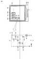
有機EL表示装置1は、図1に示すように、画像を表示するアクティブエリア102を有するアレイ基板(第1基板)100を備えている。アクティブエリア102は、マトリクス状に配置された複数の画素PXによって構成されている。また、図1では、カラー表示タイプの有機EL表示装置1を例に示しており、アクティブエリア102は、複数種類の色画素、例えば3原色に対応した赤色画素PXR、緑色画素PXG、及び、青色画素PXBによって構成されている。 As shown in FIG. 1, the organic
アレイ基板100の少なくともアクティブエリア102は、封止基板200(第2基板)によって封止されている。封止基板200は、光透過性を有する絶縁性の基板、特にガラス基板によって構成されている。この封止基板200のアレイ基板100と対向する内面は、平坦に形成されていても良いし、少なくともアクティブエリア102との対向面が窪み、周縁部より肉薄に形成されても良い。 At least the
これらのアレイ基板100と封止基板200とは、それぞれの周縁部がアクティブエリア102を囲むように枠状に配置されたシール部材300によって接合されている。この実施の形態においては、シール部材300は、フリットガラス(低融点ガラス)からなる。 The
各画素PX(R、G、B)は、画素回路10及びこの画素回路10によって駆動制御される表示素子40を備えている。図1に示した画素回路10は、一例であって、他の構成の画素回路を適用しても良いことは言うまでもない。 Each pixel PX (R, G, B) includes a
図1に示した例では、画素回路10は、駆動トランジスタDRT、各種スイッチ(第1スイッチSW1、第2スイッチSW2、第3スイッチSW3)、蓄積容量素子Csなどを備えて構成されている。駆動トランジスタDRTは、表示素子40に供給する電流量を制御する機能を有している。第1スイッチSW1及び第2スイッチSW2は、サンプル・ホールドスイッチとして機能する。第3スイッチ素子SW3は、駆動トランジスタDRTから表示素子40への駆動電流の供給、つまり表示素子40のオン/オフを制御する機能を有している。蓄積容量素子Csは、駆動トランジスタDRTのゲートーソース間の電位を保持する機能を有している。 In the example illustrated in FIG. 1, the
駆動トランジスタDRTは、高電位電源線P1と第3スイッチSW3との間に接続されている。表示素子40は、第3スイッチSW3と低電位電源線P2との間に接続されている。第1スイッチSW1及び第2スイッチSW2のゲート電極は、第1ゲート線GL1に接続されている。第3スイッチSW3のゲート電極は、第2ゲート線GL2に接続されている。第1スイッチSW1のソース電極は、映像信号線SLに接続されている。 The drive transistor DRT is connected between the high potential power supply line P1 and the third switch SW3. The
これらの駆動トランジスタDRT、第1スイッチSW1、第2スイッチSW2、及び、第3スイッチ素子SW3は、例えば薄膜トランジスタ(TFT)によって構成され、その半導体層は、アモルファスシリコンやポリシリコンなどによって形成可能であり、ここではポリシリコンによって形成されている。 The drive transistor DRT, the first switch SW1, the second switch SW2, and the third switch element SW3 are configured by, for example, a thin film transistor (TFT), and the semiconductor layer can be formed by amorphous silicon, polysilicon, or the like. Here, it is formed of polysilicon.
このような回路構成の場合、第1ゲート線GL1からオン信号が供給されたのに基づいて第1スイッチSW1及び第2スイッチSW2がオンとなり、映像信号線SLを流れる電流量に応じて高電位電源線P1から駆動トランジスタDRTに電流が流れ、また、駆動トランジスタDRTを流れる電流に応じて蓄積容量素子CSが充電される。これにより、駆動トランジスタDRTは、映像信号線SLから供給された電流量と同一の電流量を、高電位電源線P1から表示素子40に供給可能となる。 In the case of such a circuit configuration, the first switch SW1 and the second switch SW2 are turned on based on the ON signal supplied from the first gate line GL1, and the high potential is set according to the amount of current flowing through the video signal line SL. A current flows from the power supply line P1 to the drive transistor DRT, and the storage capacitor element CS is charged according to the current flowing through the drive transistor DRT. As a result, the drive transistor DRT can supply the same amount of current as that supplied from the video signal line SL to the
そして、第2ゲート線GL2からオン信号が供給されたのに基づいて第3スイッチSW3がオンとなり、蓄積容量素子CSで保持した容量に応じて、駆動トランジスタDRTは、高電位電源線P1から第3スイッチSW3を介して表示素子40に所定輝度に対応した所定量の電流を供給する。これにより、表示素子40は、所定の輝度に発光する。 Then, the third switch SW3 is turned on based on the ON signal supplied from the second gate line GL2, and the driving transistor DRT is connected to the first potential from the high potential power supply line P1 according to the capacitance held in the storage capacitor element CS. A predetermined amount of current corresponding to a predetermined luminance is supplied to the
表示素子40は、自発光性の表示素子である有機EL素子40(R、G、B)によって構成されている。すなわち、赤色画素PXRは、主に赤色波長に対応した光を出射する有機EL素子40Rを備えている。緑色画素PXGは、主に緑色波長に対応した光を出射する有機EL素子40Gを備えている。青色画素PXBは、主に青色波長に対応した光を出射する有機EL素子40Bを備えている。 The
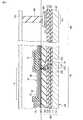
各種有機EL素子40(R、G、B)は、基本的に同一構成であり、例えば、図2に示すように、配線基板120上に配置されている。なお、配線基板120は、ガラス基板などの絶縁性の支持基板101上に、アンダーコート層111、ゲート絶縁膜112、層間絶縁膜113、有機絶縁膜(平坦化層)114などの絶縁層を備える他に、各種スイッチSW、駆動トランジスタDRT、蓄積容量素子Cs、各種配線(ゲート線、映像信号線、電源線等)などを備えて構成されている。アンダーコート層111、ゲート絶縁膜112、及び、層間絶縁膜113は、例えば、窒化シリコン(SiN)や酸化シリコン(SiO)などの無機系材料によって形成されている。 The various organic EL elements 40 (R, G, B) have basically the same configuration, and are disposed on the
すなわち、図2に示した例では、アンダーコート層111の上には、スイッチや駆動トランジスタなどのトランジスタ素子(図1に示した回路構成においては第3スイッチSW3に相当する)20の半導体層21が配置されている。半導体層21は、ゲート絶縁膜112によって覆われている。 That is, in the example shown in FIG. 2, on the
ゲート絶縁膜112の上には、トランジスタ素子20のゲート電極20Gや図示しないゲート線などが配置されている。ゲート電極20Gやゲート線は、層間絶縁膜113によって覆われている。層間絶縁膜113の上には、トランジスタ素子20のソース電極20S及びドレイン電極20Dや図示しない信号線などが配置されている。 On the
これらのソース電極20S及びドレイン電極20Dは、ゲート絶縁膜112及び層間絶縁膜113を半導体層21まで貫通するコンタクトホールを介して半導体層21にそれぞれコンタクトしている。これらのソース電極20S及びドレイン電極20Dや信号線は、有機絶縁膜114によって覆われている。このような有機絶縁膜114は、下層の凹凸の影響を緩和しその表面を平坦化する目的で、樹脂材料をコーティングするなどの手法により形成されている。 The source electrode 20S and the
この実施の形態においては、有機EL素子40は、有機絶縁膜114の上に配置されている。この有機EL素子40は、第1電極60と第2電極64との間に有機活性層62を保持した構成であり、以下に詳細な構造について説明する。 In this embodiment, the
すなわち、第1電極60は、有機絶縁膜114の上において各画素PXに独立した島状に配置され、陽極として機能する。この第1電極60は、有機絶縁膜114をドレイン電極20Dまで貫通するコンタクトホールを介して、ドレイン電極20Dにコンタクトしている。 That is, the
このような第1電極60は、アルミニウム(Al)や銀(Ag)などの光反射性を有する導電材料を用いて形成された反射層の上に、インジウム・ティン・オキサイド(ITO)やインジウム・ジンク・オキサイド(IZO)などの光透過性を有する導電材料を用いて形成された透過層を積層した構造であってもよいし、反射層単層、または、透過層単層として構成しても良い。トップエミッション方式の場合、第1電極60は、反射層を含んでいることが望ましい。 Such a
有機活性層62は、第1電極60の上に配置され、少なくとも発光層を含んでいる。この有機活性層62は、発光層以外の機能層を含むことができ、例えば、ホール注入層、ホール輸送層、ブロッキング層、電子輸送層、電子注入層、バッファ層などの機能層を含むことができる。このような有機活性層62は、複数の機能層を複合した単層で構成されても良いし、各機能層を積層した多層構造であっても良い。有機活性層62においては、発光層が有機系材料であればよく、発光層以外の層は無機系材料でも有機系材料でも構わない。有機活性層62において、発光層以外の機能層は共通層であってもよい。発光層は、赤、緑、または青に発光する発光機能を有した有機化合物によって形成される。なお、有機活性層62は、低分子系材料によって形成された薄膜を含んでいても良い。このような薄膜は、マスク蒸着法などの手法により成膜可能である。 The organic
第2電極64は、複数の画素PXに共通であって、各画素PXの有機活性層62の上に配置され、陰極として機能する。このような第2電極64は、銀(Ag)とマグネシウム(Mg)との混合物などからなる半透過層、及び、ITOなどの光透過性を有する導電材料を用いて形成された透過層を積層した構造であってもよいし、半透過層単層、または、透過層単層として構成しても良い。トップエミッション方式の場合、第2電極64は、半透過層を含んでいることが望ましい。 The
また、アレイ基板100は、アクティブエリア102において、隣接する画素PX(R、G、B)間を分離する隔壁70を備えている。この隔壁70は、例えば、各第1電極60の周縁を覆うように配置され、アクティブエリア102において格子状またはストライプ状に形成されている。これにより、隣接する異なる色の有機EL素子が絶縁される。このような隔壁70は、例えば樹脂材料をパターニングすることによって形成される。この隔壁70は、第2電極64によって覆われている。 Further, the
封止基板200は、アレイ基板100の有機EL素子40に対向するように配置されている。これらのアレイ基板100と封止基板200とは、アクティブエリアの周辺104において、シール部材300により接合されている。シール部材300は、フリットガラスであり、このようなフリットガラスは、レーザー光を照射するなどして熱を加えることによって溶融し、アレイ基板100と封止基板200とを接合する。これにより、アレイ基板100と封止基板200との間に密閉空間が形成される。有機EL素子40は、この密閉空間内に配置され、密封されることになる。 The sealing
ところで、この実施の形態においては、アレイ基板100は、シール部材300の下地として、金属層500及び金属酸化物層600の積層体を備えている。この金属層500は、アクティブエリア102の周辺104に配置され、光反射性を有する金属材料によって形成されている。また、金属酸化物層600は、金属層500の上に積層され、光透過性を有する金属酸化物によって形成されている。シール部材300は、金属酸化物層600に溶着されている。換言すると、金属層500とシール部材300とは、金属酸化物層600を介して溶着されている。 By the way, in this embodiment, the
例えば、図2に示すように、アンダーコート層111、ゲート絶縁膜112、及び、層間絶縁膜113は、アクティブエリア102からその周辺104に延在しており、シール部材300が配置されるシール領域310にも配置されている。金属層500は、シール領域310に対応するように、層間絶縁膜113の上に配置されている。金属酸化物層600は、金属層500の上に積層配置されている。 For example, as shown in FIG. 2, the
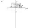
このような金属層500及び金属酸化物層600は、例えば、図3に示すように、アクティブエリア102を囲むように一連の枠状に配置されている。この場合、金属酸化物層600は、シール部材300と全周にわたって重なっている。なお、金属層500及び金属酸化物層600は、このような配置に限らず、一連でなくても良い。例えば、金属層500及び金属酸化物層600は、島状に形成され、アクティブエリア102を囲むように点在するように配置されても良いし、アクティブエリア102に沿った少なくとも一辺に配置されても良いし、特に強固な接合が要求されるコーナー部などの特定の箇所についてのみ配置されても良い。 The
このような金属酸化物層600は、シール領域310において、アレイ基板100の表面に露出している。このため、シール部材300として、フリットガラスを塗布、硬化させた封止基板200をアレイ基板100に貼り合わせる際、シール部材300は、金属酸化物層600に接触する。 Such a
そして、封止基板200の外面側からレーザー光を照射することによって、フリットガラス300を加熱し、また一部のレーザー光が金属酸化物層600を透過して金属層500によって反射されるなどしてフリットガラス300と金属酸化物層600との界面の温度上昇によってフリットガラス300が溶融し、フリットガラス300が金属酸化物層600に溶着される。 Then, the
このような金属酸化物層600は、金属層500よりも比較的高い融点を有している。このため、金属酸化物層600がフリットガラス300の下地としてのバッファ層として機能し、金属層500の溶着時の熱によるダメージを軽減できる。これにより、レーザー光を照射した際に、金属層500と金属酸化物層600との界面での剥離や界面形状乱れを抑制することが可能となる。 Such a
また、金属酸化物層600が光透過性を有するため、照射されたレーザー光は、金属酸化物層600を透過し、金属層500で反射されるため、フリットガラス300にレーザー光のエネルギーが効率よく吸収される。このため、フリットガラス300の溶融が促進され、金属酸化物層600との溶着性が向上し、アレイ基板100と封止基板200とを強固に接合することが可能となる。 In addition, since the
加えて、金属層500の上に金属酸化物層600が積層された構造においては、高い熱伝導性を維持できるため、レーザー光が照射された領域のみが局所的に高温にならず、フリットガラス300と接触している部分が均一な熱分布となる。このため、フリットガラス300と金属酸化物層600との均一な溶着が可能となる。 In addition, in the structure in which the
したがって、アレイ基板100と封止基板200とを接合するために、シール領域310を大幅に拡大する必要がなく、狭額縁化が可能となる。また、機械的強度及び密封性能を向上することが可能となり、製造歩留まりの低下を抑制できるとともに、有機EL素子の劣化が抑制されるため、良好な表示品位の維持及び長寿命化が可能となる。 Therefore, in order to join the
≪構成例≫
金属層500は、アルミニウム(Al)、銀(Ag)、アルミニウム・ネオジム(AlNd)などのアルミニウム合金のいずれかによって形成されることが望ましい。このような金属層500は、例えば、金属層500を形成する金属材料をマグネトロンスパッタ法などで成膜した後に、フォトグラフィー法やドライエッチングあるいはウエットエッチングなどにより所望の形状にパターニングされることによって形成可能である。≪Configuration example≫
The
金属酸化物層600は、インジウム・錫酸化物(ITO)、インジウム酸化物(In2O3)、亜鉛酸化物(ZnO)、チタン酸化物(TiO2)のいずれかによって形成されることが望ましい。このような金属酸化物層600は、金属層500を形成した後に、たとえば、金属酸化物層を形成する材料をスパッタ法などで成膜した後に、パターニングすることによって形成可能である。The
このようにして形成された金属酸化物層600は、例えば図4に示すように、先に形成された金属層500の表面(つまり上面及び側面)を覆うように配置される。 The
金属層500及び金属酸化物層600を形成する金属材料として、上述した材料を選択した場合には、金属層500及び金属酸化物層600は、アレイ基板100に備えられた配線または有機EL素子40を構成する電極を形成する工程で同時に形成可能である。図2に示したように、金属層500が層間絶縁膜113の上に配置された構成では、金属層500及び金属酸化物層600は、アレイ基板100における層間絶縁膜113よりも後に形成される配線または電極と同一材料によって形成可能である。 When the above-described materials are selected as the metal material for forming the
例えば、有機絶縁膜114の上に配置される第1電極60が反射層及びこの反射層の上に透過層を積層した構成においては、反射層がアルミニウムや銀を主金属として形成される場合には、金属層500は、第1電極60の反射層と同一材料により同一工程で形成可能である。また、第1電極60の透過層がITOなどによって形成される場合には、金属酸化物層600は、透過層と同一材料により同一工程で形成可能である。 For example, in the configuration in which the
これにより、金属層500及び金属酸化物層600を形成する工程を別途に必要とせず、製造工程が増加しないため、コストアップを抑制できる。 Thereby, a process for forming the
なお、金属層500については、層間絶縁膜113の上に配置される信号線やトランジスタ素子のソース電極及びドレイン電極と同一材料により同一工程で形成可能である。すなわち、配線や電極の材料としては、チタン、アルミニウムのほかに、MoTa、MoW、Mo/Al/Mo、Cr/Al/Cr、Ti/Al/Tiなどが利用可能であり、いずれも金属層500を形成する材料として適用可能である。 Note that the
次に、実施例について説明する。 Next, examples will be described.
すなわち、封止基板200となる厚さ0.7mmの平板状のガラス板の周縁部に、粘度1,000〜50,000cPのペースト状にしたフリットガラス300を、0.5mmの幅に塗布できるよう適当な塗布条件を設定し、アレイ基板100のアクティブエリア102の外周を囲む形状となるよう塗布する。フリットガラス300を塗布したガラス板を、300℃以上の温度で加熱してペースト中の有機物質を燃焼させ、フリットガラス300を硬化させる。 That is, the fritted
一方で、アレイ基板100の形成過程において、アクティブエリア102においては有機絶縁膜114の上、及び、周辺104においては層間絶縁膜113の上に、金属材料としてアルミニウム(Al)をマグネトロンスパッタ法により成膜した後に、フォトリソグラフィー法およびドライエッチング(またはウェットエッチング)により所望の形状にパターニングする。これにより、アクティブエリア102においては、第1電極60の反射層が形成されるとともに、周辺104のシール領域(溶着領域)310においては、0.7mmの幅でアクティブエリア102を囲むようなリング状の金属層500が形成される。 On the other hand, in the process of forming the
その後、基板上のアクティブエリア102及びその周辺104の全面に、ITOをスパッタ法で成膜した後に、所望の形状にパターニングする。この後、220℃でアニールして膜界面を安定化させ、透過率の向上を図る。これにより、アクティブエリア102においては、第1電極60の反射層の上に透過層が形成されるとともに、周辺104のシール領域(溶着領域)310においては、金属層500の上に金属酸化物層600が形成される。 Thereafter, ITO is deposited on the entire surface of the
その後、アクティブエリア102において、第1電極60と第2電極64との間に有機活性層62を保持した有機EL素子40と、隣接する有機EL素子を分離する隔壁70を形成するなどしてアレイ基板100が完成する。 Thereafter, in the
その後、アレイ基板100と、フリットガラス300を硬化させた封止基板200とを対向配置し、シール領域310において、金属酸化物層600とフリットガラスとを接触させた後、封止基板200側からシール領域310の金属層500に向けてレーザー光を照射してフリットガラス300を溶融し、フリットガラス300と金属酸化物層600とを溶着する。これにより、アレイ基板100と封止基板200との外周全部が接合され、アレイ基板100の有機EL素子40が密封される。 Thereafter, the
この実施例によれば、フリットガラス300を溶融するために、シール領域310に向けて照射されたレーザー光は、金属酸化物層600を透過した後に金属層500によって反射され、フリットガラス300にレーザー光のエネルギーが十分に吸収される。このため、金属酸化物層600上において、フリットガラス300の加熱及び溶融が促進される。これにより、金属酸化物層600の表面で溶融したフリットガラス300が広がり、フリットガラス300と金属酸化物層600との溶着性が向上する。したがって、溶着後のアレイ基板100と封止基板200との接合強度を向上することが可能となる。 According to this embodiment, in order to melt the
なお、この発明は、上記実施形態そのままに限定されるものではなく、その実施の段階ではその要旨を逸脱しない範囲で構成要素を変形して具体化できる。また、上記実施形態に開示されている複数の構成要素の適宜な組み合せにより種々の発明を形成できる。例えば、実施形態に示される全構成要素から幾つかの構成要素を削除してもよい。更に、異なる実施形態に亘る構成要素を適宜組み合せてもよい。 Note that the present invention is not limited to the above-described embodiment as it is, and can be embodied by modifying the constituent elements without departing from the spirit of the invention in the stage of implementation. Further, various inventions can be formed by appropriately combining a plurality of constituent elements disclosed in the embodiment. For example, some components may be deleted from all the components shown in the embodiment. Furthermore, you may combine suitably the component covering different embodiment.
1…有機EL表示装置 PX(R、G、B)…画素
40…有機EL素子(表示素子)
60…第1電極 62…有機活性層 64…第2電極
70…隔壁
100…アレイ基板 102…アクティブエリア 104…アクティブエリア周辺
120…配線基板 200…封止基板 300…シール部材(フリットガラス)
500…金属層 600…金属酸化物層DESCRIPTION OF
DESCRIPTION OF
500 ...
Claims (6)
Translated fromJapanese各画素に配置された自発光性の表示素子と、前記アクティブエリアの周辺に配置された光反射性を有する金属層と、前記金属層に積層され光透過性を有する金属酸化物層と、を備えた第1基板と、
前記第1基板の前記表示素子に対向して配置された第2基板と、
前記アクティブエリアを囲むように枠状に配置され、前記金属酸化物層に溶着されたフリットガラスからなり、前記第1基板と前記第2基板とを接合するシール部材と、
を備えたことを特徴とする表示装置。A display device having an active area composed of a plurality of pixels,
A self-luminous display element disposed in each pixel; a light-reflective metal layer disposed around the active area; and a light-transmissive metal oxide layer stacked on the metal layer. A first substrate provided;
A second substrate disposed opposite to the display element of the first substrate;
A frit glass which is arranged in a frame shape so as to surround the active area and is welded to the metal oxide layer, and a seal member which joins the first substrate and the second substrate;
A display device comprising:
反射層及び反射層の上に積層された透過層を有する第1電極と、
前記第1電極の透過層上に配置された有機活性層と、
前記有機活性層を覆うように配置された第2電極と、を備えたトップエミッション方式であり、
前記金属層は、前記第1電極の反射層と同一材料によって形成されるとともに、前記金属酸化物層は、前記第1電極の透過層と同一材料によって形成されたことを特徴とする請求項1に記載の表示装置。The display element is
A first electrode having a reflective layer and a transmissive layer laminated on the reflective layer;
An organic active layer disposed on the transmission layer of the first electrode;
A second emission electrode disposed so as to cover the organic active layer, and a top emission method.
The metal layer is formed of the same material as the reflective layer of the first electrode, and the metal oxide layer is formed of the same material as the transmissive layer of the first electrode. The display device described in 1.
Priority Applications (2)
| Application Number | Priority Date | Filing Date | Title |
|---|---|---|---|
| JP2008249009AJP2010080341A (en) | 2008-09-26 | 2008-09-26 | Display |
| US12/489,499US20100079065A1 (en) | 2008-09-26 | 2009-06-23 | Display device |
Applications Claiming Priority (1)
| Application Number | Priority Date | Filing Date | Title |
|---|---|---|---|
| JP2008249009AJP2010080341A (en) | 2008-09-26 | 2008-09-26 | Display |
Publications (1)
| Publication Number | Publication Date |
|---|---|
| JP2010080341Atrue JP2010080341A (en) | 2010-04-08 |
Family
ID=42056681
Family Applications (1)
| Application Number | Title | Priority Date | Filing Date |
|---|---|---|---|
| JP2008249009AWithdrawnJP2010080341A (en) | 2008-09-26 | 2008-09-26 | Display |
Country Status (2)
| Country | Link |
|---|---|
| US (1) | US20100079065A1 (en) |
| JP (1) | JP2010080341A (en) |
Cited By (11)
| Publication number | Priority date | Publication date | Assignee | Title |
|---|---|---|---|---|
| JP2011070797A (en)* | 2009-09-24 | 2011-04-07 | Toshiba Corp | Method for manufacturing sealing body, and organic el device |
| JP2012023038A (en)* | 2010-07-12 | 2012-02-02 | Samsung Mobile Display Co Ltd | Organic light-emitting apparatus and method of manufacturing the same |
| JP2013020964A (en)* | 2011-06-16 | 2013-01-31 | Semiconductor Energy Lab Co Ltd | Method for manufacturing sealing body, sealing body, method for manufacturing light-emitting device, and light-emitting device |
| JP2014044936A (en)* | 2012-07-30 | 2014-03-13 | Semiconductor Energy Lab Co Ltd | Encapsulation body, and organic electroluminescence device |
| JP2014067484A (en)* | 2012-09-24 | 2014-04-17 | Semiconductor Energy Lab Co Ltd | Method of producing sealing body, and sealing device |
| US9048350B2 (en) | 2011-11-28 | 2015-06-02 | Semiconductor Energy Laboratory Co., Ltd. | Sealed body, light-emitting module and method of manufacturing sealed body |
| US9214643B2 (en) | 2011-11-29 | 2015-12-15 | Semiconductor Energy Laboratory Co., Ltd. | Sealed structure, light-emitting device, electronic device, and lighting device |
| US9216557B2 (en) | 2011-11-29 | 2015-12-22 | Semiconductor Energy Laboratory Co., Ltd. | Sealed structure, light-emitting device, electronic device, and lighting device |
| US9633871B2 (en) | 2011-08-24 | 2017-04-25 | Semiconductor Energy Laboratory Co., Ltd. | Light-emitting device |
| CN108428804A (en)* | 2018-04-19 | 2018-08-21 | 武汉华星光电技术有限公司 | Oled display panel and its packaging method |
| US10068926B2 (en) | 2011-05-05 | 2018-09-04 | Semiconductor Energy Laboratory Co., Ltd. | Semiconductor device and method for manufacturing the same |
Families Citing this family (15)
| Publication number | Priority date | Publication date | Assignee | Title |
|---|---|---|---|---|
| TWI540931B (en) | 2010-04-01 | 2016-07-01 | 友達光電股份有限公司 | Organic electroluminescent device package and method of manufacturing same |
| CN101826601B (en)* | 2010-04-13 | 2012-12-12 | 友达光电股份有限公司 | Organic electroluminescent element packaging and manufacturing method thereof |
| KR102001815B1 (en) | 2011-11-29 | 2019-07-19 | 가부시키가이샤 한도오따이 에네루기 켄큐쇼 | Method of manufacturing sealed body and method of manufacturing light-emitting device |
| KR101987423B1 (en)* | 2012-11-16 | 2019-06-11 | 삼성디스플레이 주식회사 | Organic light emitting diode display and manufacturing method thereof |
| CN103219474B (en)* | 2013-03-25 | 2016-03-23 | 京东方科技集团股份有限公司 | A kind of substrate packaging method |
| KR102126714B1 (en)* | 2013-09-03 | 2020-06-26 | 삼성디스플레이 주식회사 | Display panel and organic light emitting display apparatus comprising the same |
| KR102240894B1 (en)* | 2014-02-26 | 2021-04-16 | 삼성디스플레이 주식회사 | Display device and method of manufacturing a display device |
| KR102309620B1 (en)* | 2014-11-18 | 2021-10-07 | 삼성디스플레이 주식회사 | Organic light emitting display apparatus and method for manufacturing the same |
| CN104867960B (en)* | 2015-04-21 | 2019-06-04 | 京东方科技集团股份有限公司 | Display panel and packaging method thereof, and display device |
| KR102439308B1 (en)* | 2015-10-06 | 2022-09-02 | 삼성디스플레이 주식회사 | display |
| KR102568631B1 (en)* | 2016-04-15 | 2023-08-21 | 삼성디스플레이 주식회사 | Organic light emitting diode display device |
| KR102495122B1 (en)* | 2018-01-23 | 2023-02-03 | 삼성디스플레이 주식회사 | Display device |
| JP7057740B2 (en)* | 2018-08-30 | 2022-04-20 | 株式会社ジャパンディスプレイ | Display device |
| KR102663522B1 (en)* | 2018-11-05 | 2024-05-16 | 삼성디스플레이 주식회사 | Display device and method for manufacturing of the same |
| KR102627937B1 (en) | 2018-11-27 | 2024-01-23 | 삼성디스플레이 주식회사 | Display panel |
Family Cites Families (4)
| Publication number | Priority date | Publication date | Assignee | Title |
|---|---|---|---|---|
| US6605826B2 (en)* | 2000-08-18 | 2003-08-12 | Semiconductor Energy Laboratory Co., Ltd. | Light-emitting device and display device |
| US6825496B2 (en)* | 2001-01-17 | 2004-11-30 | Semiconductor Energy Laboratory Co., Ltd. | Light emitting device |
| JP3995476B2 (en)* | 2001-12-28 | 2007-10-24 | 三洋電機株式会社 | Display device and manufacturing method thereof |
| US20060273717A1 (en)* | 2005-06-03 | 2006-12-07 | Jian Wang | Electronic device including workpieces and a conductive member therebetween |
- 2008
- 2008-09-26JPJP2008249009Apatent/JP2010080341A/ennot_activeWithdrawn
- 2009
- 2009-06-23USUS12/489,499patent/US20100079065A1/ennot_activeAbandoned
Cited By (18)
| Publication number | Priority date | Publication date | Assignee | Title |
|---|---|---|---|---|
| JP2011070797A (en)* | 2009-09-24 | 2011-04-07 | Toshiba Corp | Method for manufacturing sealing body, and organic el device |
| JP2012023038A (en)* | 2010-07-12 | 2012-02-02 | Samsung Mobile Display Co Ltd | Organic light-emitting apparatus and method of manufacturing the same |
| US11942483B2 (en) | 2011-05-05 | 2024-03-26 | Semiconductor Energy Laboratory Co., Ltd. | Semiconductor device and method for manufacturing the same |
| US10283530B2 (en) | 2011-05-05 | 2019-05-07 | Semiconductor Energy Laboratory Co., Ltd. | Semiconductor device and method for manufacturing the same |
| US10068926B2 (en) | 2011-05-05 | 2018-09-04 | Semiconductor Energy Laboratory Co., Ltd. | Semiconductor device and method for manufacturing the same |
| JP2013020964A (en)* | 2011-06-16 | 2013-01-31 | Semiconductor Energy Lab Co Ltd | Method for manufacturing sealing body, sealing body, method for manufacturing light-emitting device, and light-emitting device |
| US9633871B2 (en) | 2011-08-24 | 2017-04-25 | Semiconductor Energy Laboratory Co., Ltd. | Light-emitting device |
| US9048350B2 (en) | 2011-11-28 | 2015-06-02 | Semiconductor Energy Laboratory Co., Ltd. | Sealed body, light-emitting module and method of manufacturing sealed body |
| US10096741B2 (en) | 2011-11-28 | 2018-10-09 | Semiconductor Energy Laboratory Co., Ltd. | Sealed body, light-emitting module, and method of manufacturing sealed body |
| US9216557B2 (en) | 2011-11-29 | 2015-12-22 | Semiconductor Energy Laboratory Co., Ltd. | Sealed structure, light-emitting device, electronic device, and lighting device |
| US9214643B2 (en) | 2011-11-29 | 2015-12-15 | Semiconductor Energy Laboratory Co., Ltd. | Sealed structure, light-emitting device, electronic device, and lighting device |
| US9761827B2 (en) | 2011-11-29 | 2017-09-12 | Semiconductor Energy Laboratory Co., Ltd. | Sealed structure, light-emitting device, electronic device, and lighting device |
| US10361392B2 (en) | 2011-11-29 | 2019-07-23 | Semiconductor Energy Laboratory Co., Ltd. | Sealed structure, light-emitting device, electronic device, and lighting device |
| US11101444B2 (en) | 2011-11-29 | 2021-08-24 | Semiconductor Energy Laboratory Co., Ltd. | Sealed structure, light-emitting device, electronic device, and lighting device |
| US9853242B2 (en) | 2012-07-30 | 2017-12-26 | Semiconductor Energy Laboratory Co., Ltd. | Sealing structure and organic electroluminescence device |
| JP2014044936A (en)* | 2012-07-30 | 2014-03-13 | Semiconductor Energy Lab Co Ltd | Encapsulation body, and organic electroluminescence device |
| JP2014067484A (en)* | 2012-09-24 | 2014-04-17 | Semiconductor Energy Lab Co Ltd | Method of producing sealing body, and sealing device |
| CN108428804A (en)* | 2018-04-19 | 2018-08-21 | 武汉华星光电技术有限公司 | Oled display panel and its packaging method |
Also Published As
| Publication number | Publication date |
|---|---|
| US20100079065A1 (en) | 2010-04-01 |
Similar Documents
| Publication | Publication Date | Title |
|---|---|---|
| JP2010080341A (en) | Display | |
| JP2010080339A (en) | Display | |
| US11569474B2 (en) | Organic light-emitting diode (OLED) display and method of fabricating the same | |
| US8120249B2 (en) | Organic light emitting display and method of fabricating the same | |
| JP4964606B2 (en) | Organic light-emitting display device and method for manufacturing the same | |
| US20150155527A1 (en) | Organic light-emitting display device and method of manufacturing the same | |
| CN102044555A (en) | Organic light emitting diode display | |
| KR20150042367A (en) | Organic electro luminescent device and method of fabricating the same | |
| TW201240076A (en) | Organic el display device and method for producing same | |
| JP7075039B2 (en) | OLED display device and its manufacturing method | |
| JP2009076437A (en) | Display device | |
| JP2009259731A (en) | Light emitting device and method of manufacturing the same | |
| JP2010080344A (en) | Display | |
| WO2009104563A1 (en) | Organic el display and manufacturing method thereof | |
| JP2010092665A (en) | Organic electroluminescent display | |
| KR20110035444A (en) | Method of fabricating for dual panel type organic electro-luminescent device | |
| JP2008076987A (en) | Organic EL display panel and manufacturing method thereof | |
| JP2010080340A (en) | Display device | |
| JP2009064631A (en) | Manufacturing apparatus of display device | |
| JP2009181865A (en) | Display device | |
| JP5127657B2 (en) | Manufacturing method of organic EL display device | |
| KR102047746B1 (en) | Organic electro-luminescent device and methode of fabricating the same | |
| KR102122924B1 (en) | Organic light emitting display device and method of fabricating the same | |
| JP2010080345A (en) | Display device, and method of manufacturing the same | |
| JP2013115019A (en) | Display device |
Legal Events
| Date | Code | Title | Description |
|---|---|---|---|
| A300 | Application deemed to be withdrawn because no request for examination was validly filed | Free format text:JAPANESE INTERMEDIATE CODE: A300 Effective date:20111206 |