JP2010072110A - Liquid crystal display panel - Google Patents
Liquid crystal display panelDownload PDFInfo
- Publication number
- JP2010072110A JP2010072110AJP2008237018AJP2008237018AJP2010072110AJP 2010072110 AJP2010072110 AJP 2010072110AJP 2008237018 AJP2008237018 AJP 2008237018AJP 2008237018 AJP2008237018 AJP 2008237018AJP 2010072110 AJP2010072110 AJP 2010072110A
- Authority
- JP
- Japan
- Prior art keywords
- liquid crystal
- display panel
- crystal display
- signal lines
- interval
- Prior art date
- Legal status (The legal status is an assumption and is not a legal conclusion. Google has not performed a legal analysis and makes no representation as to the accuracy of the status listed.)
- Withdrawn
Links
Images


Landscapes
- Liquid Crystal (AREA)
Abstract
Description
Translated fromJapaneseこの発明は、液晶表示パネルに関する。 The present invention relates to a liquid crystal display panel.
一般に、液晶表示パネルは、軽量、薄型、低消費電力等の特徴を有しているため、例えば、携帯電話、携帯音楽プレーヤ等の携帯情報端末機に用いられている。特に、液晶表示パネルは、スイッチング素子として薄膜トランジスタを備えることにより高速応答性が得られる。このため、上記液晶表示パネルは、多量の情報を表示する携帯情報端末機等、電子機器の表示部に用いられている。 In general, a liquid crystal display panel has features such as light weight, thinness, and low power consumption, and thus is used in portable information terminals such as a mobile phone and a portable music player. In particular, a liquid crystal display panel can have high-speed response by including a thin film transistor as a switching element. For this reason, the liquid crystal display panel is used in a display unit of an electronic device such as a portable information terminal that displays a large amount of information.
上記液晶表示パネルは、アレイ基板と、対向基板と、液晶層とを備えている。アレイ基板は、格子状に形成された走査線及び信号線を有している。対向基板は、信号線に対向した遮光部と、遮光部に周縁を重ねた赤色、緑色及び青色の着色層とを有している。対向基板に遮光部を設ける技術は、例えば、特許文献1に開示されている。 The liquid crystal display panel includes an array substrate, a counter substrate, and a liquid crystal layer. The array substrate has scanning lines and signal lines formed in a lattice shape. The counter substrate includes a light shielding portion that faces the signal line, and red, green, and blue colored layers that overlap the light shielding portion with a peripheral edge. A technique for providing a light shielding portion on the counter substrate is disclosed in, for example,
近年、携帯情報端末機に用いられる液晶表示パネルにおいても、高輝度及び高コントラストの要求が高くなっている。しかし、上記液晶表示パネルにおいて、信号線は金属で形成されているため、黒表示時に信号線沿いで光漏れが生じてしまう。このため、画素表示領域が信号線沿いを含んでいる場合、液晶表示パネルが高コントラストを得られないという問題がある。 In recent years, liquid crystal display panels used in portable information terminals are also demanded for high brightness and high contrast. However, in the liquid crystal display panel, since the signal line is made of metal, light leakage occurs along the signal line during black display. For this reason, when the pixel display area includes along the signal line, there is a problem that the liquid crystal display panel cannot obtain high contrast.
そこで、上記問題を解決するため、遮光部の幅を大きくし、遮光部で信号線沿いを覆う技術が提案されている。これにより、高コントラスト特性を有した液晶表示パネルを得ることができる。
しかしながら、遮光部の幅を大きくし、遮光部で信号線沿いを覆った場合、開口率が大幅に低下、すなわち、画素表示領域が大幅に縮小してしまう。輝度レベルが低下してしまうため、高輝度の液晶表示パネルを得ることはできない。上記したことから、高輝度及び高コントラスト特性を有した液晶表示パネルが望まれている。
この発明は以上の点に鑑みなされたもので、その目的は、高輝度及び高トントラストを有した液晶表示パネルを提供することにある。However, when the width of the light shielding part is increased and the light shielding part covers the signal line, the aperture ratio is greatly reduced, that is, the pixel display area is significantly reduced. Since the luminance level is lowered, a high-brightness liquid crystal display panel cannot be obtained. From the above, a liquid crystal display panel having high brightness and high contrast characteristics is desired.
The present invention has been made in view of the above points, and an object thereof is to provide a liquid crystal display panel having high luminance and high ton trust.
上記課題を解決するため、本発明の態様に係る液晶表示パネルは、
第1方向に延出した複数の信号線及び前記第1方向に直交した第2方向に延出した複数の走査線を有したアレイ基板と、
前記アレイ基板に隙間を置いて対向配置された対向基板と、
前記アレイ基板及び対向基板間に挟持された液晶層と、
前記第1基板および第2基板間に設けられ、それぞれ前記第1方向に延出しているとともに前記第2方向に交互に隣接して並べられた複数色の着色層で形成されたカラーフィルタと、
前記対向基板に設けられ、それぞれ前記第1方向に延出しているとともに前記第2方向に互いに間隔を置いて並べられ、前記信号線及び着色層間の境界に重なった複数のストライプ部を有した遮光部と、を備え、
前記信号線の間隔と、前記ストライプ部の間隔と、は不等であり、
それぞれ隣合う2本の走査線、並びに隣合う2本の信号線及びストライプ部で囲まれた複数の画素表示領域は、互いに等しい面積を有している。In order to solve the above-described problems, a liquid crystal display panel according to an aspect of the present invention includes:
An array substrate having a plurality of signal lines extending in a first direction and a plurality of scanning lines extending in a second direction orthogonal to the first direction;
A counter substrate disposed opposite to the array substrate with a gap;
A liquid crystal layer sandwiched between the array substrate and the counter substrate;
A color filter formed between a plurality of colored layers provided between the first substrate and the second substrate, each extending in the first direction and arranged alternately adjacent to each other in the second direction;
A light shield having a plurality of stripe portions provided on the counter substrate, each extending in the first direction and arranged at intervals in the second direction, and overlapping a boundary between the signal line and the coloring layer. And comprising
The interval between the signal lines and the interval between the stripe portions are unequal,
A plurality of pixel display regions surrounded by two adjacent scanning lines and two adjacent signal lines and stripe portions have the same area.
この発明によれば、高輝度及び高トントラストを有した液晶表示パネルを提供することができる。 According to the present invention, a liquid crystal display panel having high brightness and high ton trust can be provided.
以下、図面を参照しながらこの発明の実施の形態に係る液晶表示パネルについて詳細に説明する。
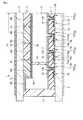
図1乃至図4に示すように、液晶表示パネルは、アレイ基板1と、このアレイ基板に所定の隙間を置いて対向配置された対向基板2と、これらアレイ基板及び対向基板間に挟持された液晶層3と、カラーフィルタ4と、第1偏光板5と、第2偏光板6とを備えている。液晶表示パネルは、矩形状の表示領域R1を備えている。Hereinafter, a liquid crystal display panel according to an embodiment of the present invention will be described in detail with reference to the drawings.
As shown in FIGS. 1 to 4, the liquid crystal display panel is sandwiched between the
アレイ基板1は、第1基板として矩形状のガラス基板10を有している。対向基板2は、第2基板として矩形状のガラス基板20を有している。第1基板及び第2基板はガラス基板に限らず、透明な絶縁基板であれば良い。表示領域R1において、液晶表示パネルは、ガラス基板10及びガラス基板20間にマトリクス状に設けられた複数の画素Pを有している。 The
アレイ基板1において、ガラス基板10上に、第1方向d1に延びているとともに第1方向と直交した第2方向d2に間隔を置いて並んだ複数の信号線11と、複数の信号線と交差して第2方向に延びているとともに第1方向に間隔を置いて並んだ複数の走査線12とが格子状に配置されている。各画素Pは、隣合う2本の信号線11及び隣合う2本の走査線12で囲まれた領域に重なって設けられている。 In the
ガラス基板10上の信号線11及び走査線12の交差部近傍に、複数のスイッチング素子として、例えば複数のTFT(薄膜トランジスタ)13が設けられている。TFT13は、走査線12の一部を延出したゲート電極13a、ゲート電極上に設けられたゲート絶縁膜13b、ゲート絶縁膜を介してゲート電極と対向したチャネル層13c、チャネル層の一方の領域に接続されたソース電極13d及びチャネル層の他方の領域に接続されたドレイン電極13eを有している。 For example, a plurality of TFTs (thin film transistors) 13 are provided as a plurality of switching elements near the intersection of the
ソース電極13dは、信号線11に接続され、ドレイン電極13eは、後述する画素電極15に接続されている。TFT13は、共通のゲート絶縁膜13bで形成されている。TFT13は画素Pに1つずつ設けられ、画素を構成している。 The
ガラス基板10、信号線11、走査線12及びTFT13上に、層間絶縁膜14が形成されている。表示領域R1において、層間絶縁膜14上に、複数の画素電極15がマトリクス状に設けられている。画素電極15は、ITO(インジウム・ティン・オキサイド)等の透明な導電材料により形成されている。各画素電極15は、層間絶縁膜14に形成されたコンタクトホール14hを介して対応するTFT13のドレイン電極13eと電気的に接続されている。画素電極15は画素Pに1つずつ設けられ、画素を構成している。 An
画素電極15上に、複数のスペーサとして、複数の柱状スペーサ16が形成されている。なお、スペーサとしては、柱状スペーサ16に限られるものではなく、球状スペーサ等他のスペーサであっても良い。層間絶縁膜14および画素電極15上に、配向膜17が成膜されている。 A plurality of
対向基板2において、ガラス基板20上に、ストライプ状の第1遮光部21と矩形枠状の第2遮光部22とが設けられている。第1遮光部21は、信号線11に重ねて形成されている。第2遮光部22は、表示領域R1を囲んで形成されている。 In the
ガラス基板20上にはカラーフィルタ4が配設されている。カラーフィルタ4は、赤色の着色層4Rと、緑色の着色層4Gと、青色の着色層4Bとを有している。 A
着色層4Rは、ストライプ状に形成され、第1方向d1に延びているとともに第2方向d2に間隔を置いて並んでいる。各着色層4Rは、その周縁部が第1遮光部21に重なって配設されている。着色層4Gは、ストライプ状に形成され、第1方向d1に延びているとともに第2方向d2に間隔を置いて並んでいる。各着色層4Gは、その周縁部が第1遮光部21に重なって配設されている。着色層4Bは、ストライプ状に形成され、第1方向d1に延びているとともに第2方向d2に間隔を置いて並んでいる。各着色層4Bは、その周縁部が第1遮光部21に重なって配設されている。 The
着色層4R、4G、4Bは、第2方向d2に交互に隣接して並べられている。画素Pは、着色層4R、4G、4Bの何れか1つを有している。
カラーフィルタ4上には、ITO等の透明な導電材料からなる対向電極23が形成されている。対向電極23上に、対向電極23上に配向膜25が成膜されている。The
On the
アレイ基板1及び対向基板2は、柱状スペーサ16により所定の隙間を置いて対向配置されている。アレイ基板1及び対向基板2は、両基板の周縁部に配設されたシール材31により互いに接合されている。液晶層3は、アレイ基板1及び対向基板2間に挟持されている。シール材31の一部には液晶注入口32が形成され、この液晶注入口は封止材33で封止されている。
第1偏光板5はガラス基板10の外面に設けられている。第2偏光板6はガラス基板20の外面に設けられている。第2偏光板6の外面は表示面である。上記したように液晶表示パネルが形成されている。The
The first
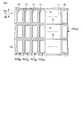
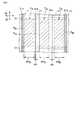
次に、上記液晶表示パネルをさらに詳細に説明する。特に、信号線11及び第1遮光部21について詳細に説明する。
図1乃至図4及び図5に示すように、信号線11間の間隔は不等である。着色層4G(緑色の画素PG)を挟んだ信号線11間の間隔p1Gは、着色層4R(赤色の画素PR)を挟んだ信号線11間の間隔p1R及び着色層4B(青色の画素PB)を挟んだ信号線11間の間隔p1Bより広い。信号線11の幅w1は、それぞれ同一である。Next, the liquid crystal display panel will be described in more detail. In particular, the
As shown in FIGS. 1 to 4 and 5, the spacing between the signal lines 11 is unequal. The interval p1G between the
この実施の形態において、間隔p1Gは、50μmであり、間隔p1R及び間隔p1Bは、それぞれ35μmである。なお、走査線12間の間隔p2は、120μmであり、信号線11の幅w1は、それぞれ8μmである。In this embodiment, the interval p1G is 50 μm, and the interval p1R and the interval p1B are each 35 μm. The interval p2 between the scanning lines 12 is 120 μm, and the width w1 of the
図1乃至図4及び図6に示すように、第1遮光部21は、複数のストライプ部21aを有している。ストライプ部21aは、それぞれ第1方向d1に延出しているとともに第2方向d2に互いに間隔を置いて並べられている。ストライプ部21aは、信号線11に重なっている。さらに、ストライプ部21aは、着色層4R、4G、4B間の境界にも重なっている。 As shown in FIGS. 1 to 4 and 6, the first
ストライプ部21a間の間隔は不等である。着色層4G(緑色の画素PG)を挟んだストライプ部21a間の間隔p3Gは、着色層4R(赤色の画素PR)を挟んだストライプ部21a間の間隔p3R及び着色層4B(青色の画素PB)を挟んだストライプ部21a間の間隔p3Bより狭い。ストライプ部21aの幅は異なっている。着色層4G(緑色の画素PG)を挟んだストライプ部21aの幅w2aは、他のストライプ部21aの幅w2bより大きい。The spacing between the
この実施の形態において、間隔p3Gは、42μmであり、間隔p3R及び間隔p3Bは、それぞれ38μmである。なお、幅w2aは、10μmであり、幅w2bは、5μmである。In this embodiment, the interval p3G is 42 μm, and the interval p3R and the interval p3B are each 38 μm. The width w2a is 10 μm and the width w2b is 5 μm.
図1乃至図7に示すように、信号線11から外れて位置したストライプ部21aの面積は、ストライプ部21aの重なった着色層4R、4G、4Bの色毎に異なっている。ここでは、信号線11から外れて着色層4Gに重なったストライプ部21aの面積が最も大きい。また、着色層4R、4Bに重なった領域において、ストライプ部21aは信号線11から外れて位置していない。 As shown in FIGS. 1 to 7, the area of the
画素PR、PG、PBは、隣合う2本の走査線12、並びに隣合う2本の信号線11及びストライプ部21aで囲まれた画素表示領域RR、RG、RBに設けられている。画素PR、PG、PBの幅w4R、w4G、w4Bは、互いに等しい。
この実施の形態において、幅w4R、w4G、w4Bは、それぞれ20μmである。このため、画素表示領域RR、RG、RB(透過表示領域)は、互いに等しい面積を有している。PixelPR,PG,PB is adjacent two scanning
In this embodiment, the widths w4R , w4G , and w4B are each 20 μm. For this reason, the pixel display regions RR , RG , and RB (transmission display regions) have the same area.
以上のように構成された液晶表示パネルによれば、信号線11間の間隔と、ストライプ部21a間の間隔とは不等である。着色層4G(緑色の画素PG)に重なったストライプ部21aは、信号線11から外れて位置している。このため、黒表示時に表示画像に最も悪影響を及ぼす画素PGの信号線11付近からの光漏れを防止することができる。これにより、液晶表示パネルは、高コントラストを得ることができる。According to the liquid crystal display panel configured as described above, the interval between the
着色層4G(緑色の画素PG)に重なったストライプ部21aは、信号線11から外れて位置しているだけでなく、信号線11、少なくとも信号線11の側縁に重なっている。このため、アレイ基板1及び対向基板2を貼り合せる工程で位置ずれが生じた場合であっても、ストライプ部21aは、光漏れを防止することができる。The
また、着色層4Gに重なった領域においてストライプ部21aが信号線11から外れて位置した面積は、画素表示領域RGの1/3程度である。着色層4R、4Bに重なった領域において、ストライプ部21aは信号線11から外れて位置していない。ストライプ部21aによるRR、RG、RBの面積の縮小は最小限に抑えられているため、開口率の低下を最小限に抑制することができる。これにより、液晶表示パネルは、高い輝度を得ることができる。Further, the area where the
そして、信号線11間の間隔と、ストライプ部21a間の間隔とを調整したことにより、画素表示領域RR、RG、RBの面積を互いに等しくすることができる。これにより、表示品位に優れた液晶表示パネルを得ることができる。
上記したことから、高輝度及び高トントラストを有した液晶表示パネルを得ることができる。Then, the distance between the
As described above, a liquid crystal display panel having high luminance and high ton trust can be obtained.
なお、この発明は上記実施の形態そのままに限定されるものではなく、実施段階ではその要旨を逸脱しない範囲で構成要素を変形して具体化可能である。また、上記実施の形態に開示されている複数の構成要素の適宜な組み合わせにより、種々の発明を形成できる。例えば、実施形態に示される全構成要素から幾つかの構成要素を削除してもよい。 Note that the present invention is not limited to the above-described embodiment as it is, and can be embodied by modifying the constituent elements without departing from the scope of the invention in the implementation stage. Various inventions can be formed by appropriately combining a plurality of constituent elements disclosed in the embodiments. For example, some components may be deleted from all the components shown in the embodiment.
例えば、カラーフィルタ4は、対向基板2側に限らず、アレイ基板1側に設けられていても良い。 For example, the
第1遮光部21は、ストライプ状に限らず、格子状に形成されていても良い。第1遮光部21は、信号線11及び走査線12に重ねて形成される。そして、第1遮光部21により、信号線11付近からの光漏れと、走査線12付近からの光漏れを防止しても良い。The first
1…アレイ基板、2…対向基板、3…液晶層、4…カラーフィルタ、4R,4G,4B…着色層、10…ガラス基板、11…信号線、12…走査線、13…TFT、15…画素電極、20…ガラス基板、21…第1遮光部、21a…ストライプ部、22…第2遮光部、23…対向電極、R1…表示領域、RR,RG,RB…画素表示領域、P,PR,PG,PB…画素、p1R,p1G,p1B,p2,p3R,p3G,p3B…間隔、w1,w2a,w2b,w3,w4R,w4G,w4B…幅、d1…第1方向、d2…第2方向。DESCRIPTION OF
Claims (3)
Translated fromJapanese前記アレイ基板に隙間を置いて対向配置された対向基板と、
前記アレイ基板及び対向基板間に挟持された液晶層と、
前記第1基板および第2基板間に設けられ、それぞれ前記第1方向に延出しているとともに前記第2方向に交互に隣接して並べられた複数色の着色層で形成されたカラーフィルタと、
前記対向基板に設けられ、それぞれ前記第1方向に延出しているとともに前記第2方向に互いに間隔を置いて並べられ、前記信号線及び着色層間の境界に重なった複数のストライプ部を有した遮光部と、を備え、
前記信号線間の間隔と、前記ストライプ部間の間隔と、は不等であり、
それぞれ隣合う2本の走査線、並びに隣合う2本の信号線及びストライプ部で囲まれた複数の画素表示領域は、互いに等しい面積を有している液晶表示パネル。An array substrate having a plurality of signal lines extending in a first direction and a plurality of scanning lines extending in a second direction orthogonal to the first direction;
A counter substrate disposed opposite to the array substrate with a gap;
A liquid crystal layer sandwiched between the array substrate and the counter substrate;
A color filter formed between a plurality of colored layers provided between the first substrate and the second substrate, each extending in the first direction and arranged alternately adjacent to each other in the second direction;
A light shield having a plurality of stripe portions provided on the counter substrate, each extending in the first direction and arranged at intervals in the second direction, and overlapping a boundary between the signal line and the coloring layer. And comprising
The spacing between the signal lines and the spacing between the stripe portions are unequal,
A liquid crystal display panel in which a plurality of pixel display regions surrounded by two adjacent scanning lines and two adjacent signal lines and stripe portions have the same area.
前記緑色の着色層を挟んだ前記信号線間の間隔は、前記赤色の着色層を挟んだ前記信号線間の間隔及び前記青色の着色層を挟んだ前記信号線間の間隔より広く、
前記緑色の着色層を挟んだ前記ストライプ部間の間隔は、前記赤色の着色層を挟んだ前記ストライプ部間の間隔及び前記青色の着色層を挟んだ前記ストライプ部間の間隔より狭い請求項1又は2に記載の液晶表示パネル。The color filter is formed of a plurality of colored layers of red, green and blue,
An interval between the signal lines sandwiching the green colored layer is wider than an interval between the signal lines sandwiching the red colored layer and an interval between the signal lines sandwiching the blue colored layer,
2. The interval between the stripe portions sandwiching the green colored layer is narrower than the interval between the stripe portions sandwiching the red colored layer and the interval between the stripe portions sandwiching the blue colored layer. Or the liquid crystal display panel of 2.
Priority Applications (1)
| Application Number | Priority Date | Filing Date | Title |
|---|---|---|---|
| JP2008237018AJP2010072110A (en) | 2008-09-16 | 2008-09-16 | Liquid crystal display panel |
Applications Claiming Priority (1)
| Application Number | Priority Date | Filing Date | Title |
|---|---|---|---|
| JP2008237018AJP2010072110A (en) | 2008-09-16 | 2008-09-16 | Liquid crystal display panel |
Publications (1)
| Publication Number | Publication Date |
|---|---|
| JP2010072110Atrue JP2010072110A (en) | 2010-04-02 |
Family
ID=42203983
Family Applications (1)
| Application Number | Title | Priority Date | Filing Date |
|---|---|---|---|
| JP2008237018AWithdrawnJP2010072110A (en) | 2008-09-16 | 2008-09-16 | Liquid crystal display panel |
Country Status (1)
| Country | Link |
|---|---|
| JP (1) | JP2010072110A (en) |
Cited By (2)
| Publication number | Priority date | Publication date | Assignee | Title |
|---|---|---|---|---|
| WO2012053399A1 (en)* | 2010-10-18 | 2012-04-26 | シャープ株式会社 | Liquid crystal display device |
| WO2021196787A1 (en)* | 2020-03-30 | 2021-10-07 | 京东方科技集团股份有限公司 | Display substrate, display panel and display device |
- 2008
- 2008-09-16JPJP2008237018Apatent/JP2010072110A/ennot_activeWithdrawn
Cited By (2)
| Publication number | Priority date | Publication date | Assignee | Title |
|---|---|---|---|---|
| WO2012053399A1 (en)* | 2010-10-18 | 2012-04-26 | シャープ株式会社 | Liquid crystal display device |
| WO2021196787A1 (en)* | 2020-03-30 | 2021-10-07 | 京东方科技集团股份有限公司 | Display substrate, display panel and display device |
Similar Documents
| Publication | Publication Date | Title |
|---|---|---|
| US9971188B2 (en) | Display device | |
| JP5197206B2 (en) | Liquid crystal display | |
| JP4946135B2 (en) | Liquid crystal display element | |
| US9575377B2 (en) | Curved liquid crystal display | |
| US8704990B2 (en) | Electro-optical display apparatus | |
| KR100510565B1 (en) | Liquid crystal display device | |
| WO2017140000A1 (en) | Va type coa liquid crystal display panel | |
| TWI753527B (en) | Display device | |
| CN109557733B (en) | Array substrate, display panel and display device | |
| TW201622112A (en) | Display panel | |
| CN114253013A (en) | Display panel and display device | |
| JP6554403B2 (en) | Liquid crystal display | |
| JP2012098329A (en) | Liquid crystal display device | |
| TWI771244B (en) | Display device | |
| JP4306779B2 (en) | Display device | |
| US8477269B2 (en) | Liquid crystal display device | |
| JP2010072110A (en) | Liquid crystal display panel | |
| JP5075427B2 (en) | Liquid crystal display | |
| JP2011013450A (en) | Liquid crystal display device and method of manufacturing the same | |
| JP2005128424A (en) | Display apparatus | |
| US20150042912A1 (en) | Liquid crystal display apparatus | |
| KR101480841B1 (en) | Liquid crystal display device | |
| JP5555649B2 (en) | LCD panel | |
| JP4441507B2 (en) | Liquid crystal display | |
| JPH1184394A (en) | Active matrix type liquid crystal display |
Legal Events
| Date | Code | Title | Description |
|---|---|---|---|
| A300 | Withdrawal of application because of no request for examination | Free format text:JAPANESE INTERMEDIATE CODE: A300 Effective date:20111206 |