JP2010067902A - Light-emitting device - Google Patents
Light-emitting deviceDownload PDFInfo
- Publication number
- JP2010067902A JP2010067902AJP2008234874AJP2008234874AJP2010067902AJP 2010067902 AJP2010067902 AJP 2010067902AJP 2008234874 AJP2008234874 AJP 2008234874AJP 2008234874 AJP2008234874 AJP 2008234874AJP 2010067902 AJP2010067902 AJP 2010067902A
- Authority
- JP
- Japan
- Prior art keywords
- substrate
- electrode
- outer edge
- light
- light emitting
- Prior art date
- Legal status (The legal status is an assumption and is not a legal conclusion. Google has not performed a legal analysis and makes no representation as to the accuracy of the status listed.)
- Pending
Links
Images


Classifications
- H—ELECTRICITY
- H10—SEMICONDUCTOR DEVICES; ELECTRIC SOLID-STATE DEVICES NOT OTHERWISE PROVIDED FOR
- H10H—INORGANIC LIGHT-EMITTING SEMICONDUCTOR DEVICES HAVING POTENTIAL BARRIERS
- H10H20/00—Individual inorganic light-emitting semiconductor devices having potential barriers, e.g. light-emitting diodes [LED]
- H10H20/80—Constructional details
- H10H20/85—Packages
- H10H20/8506—Containers
- H—ELECTRICITY
- H01—ELECTRIC ELEMENTS
- H01L—SEMICONDUCTOR DEVICES NOT COVERED BY CLASS H10
- H01L24/00—Arrangements for connecting or disconnecting semiconductor or solid-state bodies; Methods or apparatus related thereto
- H01L24/93—Batch processes
- H01L24/95—Batch processes at chip-level, i.e. with connecting carried out on a plurality of singulated devices, i.e. on diced chips
- H01L24/97—Batch processes at chip-level, i.e. with connecting carried out on a plurality of singulated devices, i.e. on diced chips the devices being connected to a common substrate, e.g. interposer, said common substrate being separable into individual assemblies after connecting
- H—ELECTRICITY
- H01—ELECTRIC ELEMENTS
- H01L—SEMICONDUCTOR DEVICES NOT COVERED BY CLASS H10
- H01L2224/00—Indexing scheme for arrangements for connecting or disconnecting semiconductor or solid-state bodies and methods related thereto as covered by H01L24/00
- H01L2224/01—Means for bonding being attached to, or being formed on, the surface to be connected, e.g. chip-to-package, die-attach, "first-level" interconnects; Manufacturing methods related thereto
- H01L2224/42—Wire connectors; Manufacturing methods related thereto
- H01L2224/47—Structure, shape, material or disposition of the wire connectors after the connecting process
- H01L2224/48—Structure, shape, material or disposition of the wire connectors after the connecting process of an individual wire connector
- H01L2224/4805—Shape
- H01L2224/4809—Loop shape
- H01L2224/48091—Arched
- H—ELECTRICITY
- H01—ELECTRIC ELEMENTS
- H01L—SEMICONDUCTOR DEVICES NOT COVERED BY CLASS H10
- H01L2924/00—Indexing scheme for arrangements or methods for connecting or disconnecting semiconductor or solid-state bodies as covered by H01L24/00
- H01L2924/15—Details of package parts other than the semiconductor or other solid state devices to be connected
- H01L2924/151—Die mounting substrate
- H01L2924/156—Material
- H01L2924/15786—Material with a principal constituent of the material being a non metallic, non metalloid inorganic material
- H01L2924/15787—Ceramics, e.g. crystalline carbides, nitrides or oxides
Landscapes
- Engineering & Computer Science (AREA)
- Computer Hardware Design (AREA)
- Microelectronics & Electronic Packaging (AREA)
- Power Engineering (AREA)
- Led Device Packages (AREA)
- Led Devices (AREA)
Abstract
Translated fromJapaneseDescription
Translated fromJapanese本発明は、発光装置に関する。 The present invention relates to a light emitting device.
表示装置用バックライト光源に白色LEDを用いると、冷陰極管よりも低消費電力化、小型化、及び薄型化が容易となる。 When a white LED is used as a backlight light source for a display device, lower power consumption, size reduction, and thickness reduction are easier than a cold cathode tube.
また、表示装置の大型化及び高精細化のために、LEDの高出力化が要求されている。このようなLEDを搭載するパッケージの材料にセラミックやガラスエポキシからなる絶縁基板を用いると、小型、薄型、及び高出力化が容易となる。 Further, in order to increase the size and definition of the display device, it is required to increase the output of the LED. When an insulating substrate made of ceramic or glass epoxy is used as a material for a package in which such an LED is mounted, it is easy to reduce the size, the thickness, and the output.
しかしながら、白色LED用パッケージの凹部内には蛍光体を分散配置した封止樹脂を充填するために、幅に対する高さの比率が大きくなる。このために、個々の発光装置に分割する場合、バリや欠けを生じ分割が困難になることがある。また、分割されたパッケージの側面が平面状とならないために、半田付け後の発光装置の光軸を所望の角度方向に揃えることが困難となる問題を生じる。 However, since the sealing resin in which the phosphors are dispersed and filled is filled in the concave portion of the white LED package, the ratio of the height to the width increases. For this reason, when dividing | segmenting into each light-emitting device, a burr | flash or a chip | tip may be produced and division may become difficult. Further, since the side surfaces of the divided packages are not flat, there arises a problem that it is difficult to align the optical axis of the light emitting device after soldering in a desired angular direction.
セラミックを用いた半導体素子用支持体に関する技術開示例がある(特許文献1)。この技術開示例によれば、セラミック基板の主面を作用点とし、曲げモーメントを加えると共に、主面に平行な方向に引っ張りモーメントを加えながらセラミック基板を分割する半導体装置が提供される。
しかしながら、この技術開示例を用いても、幅に対する厚さ比率が大きい絶縁体を積層したパッケージを確実に分割するには十分とは言えない。このために、例えば側面型発光装置を実装基板に対して所望の角度で取り付けることが困難となり、表示画面の輝度が不均一になる問題を生じる。
However, even if this example of technical disclosure is used, it cannot be said that it is sufficient to reliably divide a package in which insulators having a large thickness ratio to width are stacked. For this reason, for example, it becomes difficult to attach the side-type light emitting device at a desired angle with respect to the mounting substrate, thereby causing a problem that the luminance of the display screen is not uniform.
分割が容易で、且つ実装基板へ精度良く取り付け可能な発光装置を提供する。 Provided is a light-emitting device that can be easily divided and attached to a mounting substrate with high accuracy.
本発明の一態様によれば、分割して形成された端面を外縁に有する第1の基板と、第1の電極と、一方の端部が前記第1の電極の一方の端部と対向する第2の電極と、を上面に有し、且つ前記第1の電極と接続された第1の引き出し電極と、前記第2の電極と接続された第2の引き出し電極と、を側面の隅部に有し、外縁が前記第1の基板の前記外縁よりも内側となるように前記第1の基板の上に積層された第2の基板と、前記第1の電極に接着された発光素子と、前記発光素子からの放出光を放出可能な第1の貫通孔を有し、且つ外縁が前記第1の基板の前記外縁よりも内側となるように前記第2の基板の上に積層された第3の基板と、を備えたことを特徴とする発光装置が提供される。 According to one embodiment of the present invention, the first substrate having the end face formed by dividing the outer surface at the outer edge, the first electrode, and the one end portion are opposed to the one end portion of the first electrode. A first electrode having a second electrode on the upper surface and connected to the first electrode, and a second electrode connected to the second electrode, and a corner of the side surface A second substrate laminated on the first substrate such that an outer edge is inside the outer edge of the first substrate, and a light emitting element bonded to the first electrode And a first through hole capable of emitting light emitted from the light emitting element, and the outer edge is laminated on the second substrate so as to be inside the outer edge of the first substrate. And a third substrate. A light emitting device including the third substrate is provided.
また、本発明の他の一態様によれば、第1の電極と、一方の端部が前記第1の電極の一方の端部と対向する第2の電極と、を上面に有し、且つ前記第1の電極と接続された第1の引き出し電極と、前記第2の電極と接続された第2の引き出し電極と、を側面の隅部に有し、分割して形成された端面を外縁に有する第1の基板と、前記発光素子からの放出光を放出可能な第1の貫通孔を有し、外縁が前記第1の基板の前記外縁よりも内側となるように前記第1の基板の上方に積層された第2の基板と、を備えたことを特徴とする発光装置が提供される。 According to another aspect of the present invention, the first electrode and the second electrode having one end facing the one end of the first electrode are provided on the upper surface, and A first lead electrode connected to the first electrode and a second lead electrode connected to the second electrode are provided at the corners of the side surface, and the end face formed by division is an outer edge. A first substrate having a first through hole capable of emitting light emitted from the light emitting element, and an outer edge of the first substrate being located inside the outer edge of the first substrate. There is provided a light emitting device comprising: a second substrate stacked above.
分割が容易で、且つ実装基板へ精度良く取り付け可能な発光装置が提供される。 A light-emitting device that can be easily divided and attached to a mounting substrate with high accuracy is provided.
以下、図面を参照しつつ本発明の実施の形態について説明する。
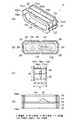
図1は、本発明の第1の実施形態にかかる発光装置の模式図を表す。すなわち、図1(a)は斜視図、図1(b)は第1の基板の平面図、図1(c)は第2の基板の平面図、及び図1(d)は第3の基板の平面図である。Hereinafter, embodiments of the present invention will be described with reference to the drawings.
FIG. 1 is a schematic view of a light emitting device according to a first embodiment of the present invention. 1A is a perspective view, FIG. 1B is a plan view of a first substrate, FIG. 1C is a plan view of a second substrate, and FIG. 1D is a third substrate. FIG.
基板の材料はAl2O3、AlNなどのセラミックやガラスエポキシなどとできるが、 図1の実施形態ではAl2O3からなるセラミックとする。図1の第1の基板10、第2の基板12、及び第3の基板14、は積層前の基板を表し、これらの基板が重ね合わされたのち焼成され積層体となり、図1(a)に表す発光装置となる。The substrate material may be ceramic such as Al2 O3 or AlN, glass epoxy, or the like, but in the embodiment shown in FIG. 1, it is a ceramic made of Al2 O3 . The
発光装置は凹部28を有しており、凹部28の底面には発光素子40が接着されている。また、発光装置の側面の隅部には、取り出し用電極20、22が設けられており、発光素子40へ電圧を供給することが可能である。 The light emitting device has a
図1(b)のように、第1の基板10は、例えば長辺が4mm、短辺が1mm、厚さが0.1mmなどとする。また、第1の基板10の上に積層される第2の基板12及び第2の基板12の上に積層される第3の基板14は、共に長辺を3.8mm、短辺を0.8mmとし、長辺及び短辺が第1の基板10よりも小さい。すなわち、積層体において、第1の基板10の外縁10mは、分割して形成された端面を有する。そして、第1の基板10の外縁10mは、第2の基板12の外縁12m及び第3の基板14の外縁14mよりも外側にあり、第2の基板12の外縁12mと第3の基板14の外縁14mとは上方から見て略一致する。 As shown in FIG. 1B, the
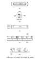
積層前の第1の基板10は、互いに略直交するV溝10cを有しており、個々の発光装置に分割する工程を容易にすることができる。図1(b)において分割数を3×3としているが、分割数を20×20のように多くすると発光装置の生産性を高めることができる。また、分割後に切り欠き部となる領域にはビアホール10aが設けられ、また各辺の略中央部にはガス抜き孔(焼結工程におけるガス抜き用)10bが設けられている。 The
図1(c)のように、第2の基板12の表面には、厚膜印刷工程を用いて第1の電極12f及び第2の電極12gが形成されており、例えば第1の電極12fの上に、発光素子40が銀ペーストなどの接着剤を用いて接着可能とされる。発光素子40の上面の電極と第2の電極12gとはボンディングワイヤ42により接続可能とされる。 As shown in FIG. 1C, the
また、第2の基板12には、第1の基板10のビアホール10a及びガス抜き孔10bと略同一の位置になるようなビアホール12a及びガス抜き孔12bが設けられている。第2の基板12が第1の基板10に重ね合わされた場合、V溝10cの直上近傍を開口部とするので、第2の基板12を構成する個々のパッケージの単位は少なくとも2つの連結部12eにより互いに連結されている。この連結部12eを、例えばガス抜き孔10bを横切るように設けると、分割が容易となる。 Further, the
第2の基板12のビアホール12aの内壁には、第1の電極12fと接続され第1の引き出し用電極22と、第2の電極12gと接続される第2の引き出し用電極20と、が側面メタライズにより形成され、実装基板へ取り付けを容易にする。 On the inner wall of the
図1(d)のように、第3の基板14は、積層体の凹部28を構成する第1の貫通孔14nを有している。凹部28には封止樹脂29が充填され、発光素子40からの放出光が上方に向かって放出可能とされる。また、第1の貫通孔14nは、例えば長径が3mm且つ短径が0.5mmなどとされる。さらに、ビアホール14a、ガス抜き孔14b、及び連結部14eが、第2の基板12と略同一の位置となるように形成されている。 As shown in FIG. 1D, the
それぞれの基板においてビアホールの内壁にメタライズをしておき積層後に分割を行うと、図1(a)のように、切り欠き部の表面全体に引き出し用電極20、22を広げることができる。このため、実装基板との半田付けを確実にできる。なお、厚膜印刷工程などを用いて形成された第1及び第2の引き出し用電極22、20の上に、例えば金メッキを行うと電極表面の酸化を抑制でき、実装基板との半田付けが確実にできるので好ましい。 When metallization is performed on the inner wall of the via hole in each substrate and division is performed after lamination, the
焼成後の積層体は、例えばローラーなどを用いてV溝10cに圧力を加えると、V溝10cを起点に分割が容易となる。この場合、第1の基板10を0.1mmと薄くすると、分割して形成された端面10mにバリや欠けなどを生じることが抑制でき確実に分割可能となり、実装基板へ精度良く取り付けることが容易となる。 When the laminated body after firing is applied with pressure to the V-
図1の発光装置は、上面発光型として用いることができる。封止樹脂29として、例えばシリコーン樹脂などを用い、その中に蛍光体粒子を分散配置すると、発光素子40からの放出光と、蛍光体粒子からの波長変換光と、の混合光を得ることができる。このようにして、例えば窒化物系半導体からなる発光素子40からの青色光と、黄色蛍光体からの黄色光との混合色として、白色光または白熱電球色を得ることができる。 The light emitting device in FIG. 1 can be used as a top emission type. When, for example, a silicone resin is used as the sealing
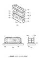
図2は、本発明の第2の実施形態にかかる発光装置の模式図である。すなわち、図2(a)は斜視図、図2(b)は平面図、図2(c)は側面図、図2(d)は正面図、をそれぞれ表す。
また、図3は、基板の模式図である。すなわち、図3(a)は第1の基板の平面図、図3(b)は第2の基板の平面図、図3(c)は第5の基板の平面図、図3(d)は第3の基板の平面図、図3(e)は第4の基板の平面図、図3(f)は分割前の積層体の側面図、をそれぞれ表す。FIG. 2 is a schematic view of a light emitting device according to the second embodiment of the present invention. 2A is a perspective view, FIG. 2B is a plan view, FIG. 2C is a side view, and FIG. 2D is a front view.
FIG. 3 is a schematic diagram of the substrate. 3A is a plan view of the first substrate, FIG. 3B is a plan view of the second substrate, FIG. 3C is a plan view of the fifth substrate, and FIG. The top view of a 3rd board | substrate, FIG.3 (e) represents the top view of a 4th board | substrate, FIG.3 (f) represents the side view of the laminated body before a division | segmentation, respectively.
本実施形態では、最下層となる第1の基板10の外縁10mと、最上層となる第4の基板16の外縁16mと、は分割して形成された端面を有する。また、複数の基板における複数の貫通孔により凹部28が構成されている。 In the present embodiment, the
第1の基板10及び第4の基板16は、例えば長辺が4mm、短辺が1mm、厚さが0.1mmとする。また、第1の基板10の上に積層される第2の基板12、第2の基板12の上に積層される第5の基板18、及び第5の基板18の上に積層される第3の基板14は、共に長辺が3.8mm、短辺が0.8mmとされ、長辺及び短辺は第1の基板10及び第4の基板16よりも小さい。すなわち、図2のように、積層体5において、第1の基板10及び第4の基板16の外縁10m、16mは分割して形成された端面を有する。外縁10m、16mは、第2、第5、及び第3の基板12、18、14の外縁12m、18m、及び14mの外側に位置する。 For example, the
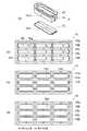
焼結工程ののち、ビアホール10a、12a、18a、14a、16a、ガス抜き孔10b、12b、18b、14b、16b、連結部12e、18e、及び14e、の位置がそれぞれ略同一となるように、それぞれの基板が形成されている。また、焼結後の積層体5を分割すると、ビアホールは側面の4つの隅部において切り欠き部となる。また、ガス抜き孔の中心線近傍に設けられた連結部は分離され、それぞれの突出部24、26を構成する。 After the sintering process, the positions of the via
また、第1の基板10のV溝10cと、第4の基板16のV溝16cと、は上方から見て略一致する(略同一の位置となる)ように積層され、V溝10cとV溝16cとの間は中空構造となっている。 Further, the V-
第2の基板12は、第1の電極12fと、第2の電極12gと、を表面に有している。ビアホール12aの内壁には、第1の電極12fと接続される第1の引き出し用電極22と、第2の電極12gと接続される第2の引き出し用電極20と、が側面メタライズにより形成されており、実装基板への電気的接続及び取り付けを容易にしている。 The
第3の基板14は第1の貫通孔14nを、第4の基板16は第1の貫通孔14n以上の大きさである第2の貫通孔16nを、第5の基板18は第1の貫通孔14nと略同一形状の第3の貫通孔18nを、それそれ有しており、これらの貫通孔が積層され焼結されると、積層体5の凹部28を形成する。 The
第3の基板14が有する貫通孔14nの内壁に、例えば銀などの金属を用いた反射層14kを形成すると発光素子40からの放出光を上方に反射でき、光取り出し効率を高めることが容易となる。この場合、第5の基板18の厚さを、例えば0.1mmなどとして、第2の基板12と第3の基板14との間に挟むように設けると第1の電極12fと、第2の電極12gと、の間の短絡を抑制するアイソレーション層として機能する。なお、第3の基板14の貫通孔14nの内壁の下部に反射層の非形成領域を設けてもアイソレーションが可能であり、この場合、第5の基板18を省略することができる。 If the
図2に表すように、この積層体5の幅Wと高さHとの比率は、1以上となることがある。
このような厚い積層体5であっても、最上層である第4の基板16と、最下層である第1の基板10との厚さを、例えば0.1mmなどと薄くすると、図3(f)のように積層体5は中空であるので、V溝10c、16cが形成されている破線で表すV−V線の方向にローラーなどを用いて圧力を加えると、分離が容易であり且つ分割して形成された端面にバリや欠けを抑制できる。As shown in FIG. 2, the ratio of the width W to the height H of the
Even in such a
このような発光装置は、側面型または上面型として用いることができる。側面型とする場合、発光装置の側面側と実装基板とを半田などを用いて接着する。すなわち、切り欠き部に設けられた引き出し用電極20、22と実装基板の導電部とをそれぞれ半田付けする。 Such a light emitting device can be used as a side surface type or a top surface type. In the case of a side surface type, the side surface side of the light emitting device and the mounting substrate are bonded using solder or the like. That is, the lead-out
側面型発光装置を表示装置のバックライト光源として用いる場合、表示装置の導光板の厚さは、例えば1mm以下である。本実施形態の発光装置の幅Wを1mm以下とすることは容易であり、導光板の側方から効率よく発光素子40の放出光を入射することができる。 When the side-type light emitting device is used as the backlight light source of the display device, the thickness of the light guide plate of the display device is, for example, 1 mm or less. It is easy to make the width W of the light emitting device of this embodiment 1 mm or less, and the light emitted from the
図4は、比較例にかかる発光装置の模式図である。すなわち、図4(a)は平面図、図4(b)は側面図、図4(c)は正面図、図4(d)はV溝を説明する図、図4(e)は実装基板へ取り付けられた状態を表す図である。 FIG. 4 is a schematic diagram of a light emitting device according to a comparative example. 4 (a) is a plan view, FIG. 4 (b) is a side view, FIG. 4 (c) is a front view, FIG. 4 (d) is a diagram for explaining a V-groove, and FIG. 4 (e) is a mounting substrate. It is a figure showing the state attached to.
第1の基板110の上にアイソレーション用の第2の基板118が積層され、第2の基板118の上に第3の基板116がさらに積層され、例えば、積層体の幅WWを1mm、高さを0.8mmなどとできる。高さが0.8mmの積層体に高さの2分の1から3分の1となる深さのV溝120、121を積層体の上側及び下側から形成し、ローラーなどを用いて分割すると、V溝に沿って分割されるが、バリや欠けなどを生じやすい。このために、実装基板へ半田付けすると、図4(e)のように、放出光の光軸が水平軸からずれやすく、バックライト光源に用いると画面の輝度が不均一となることがあり、側面型としては好ましくない。 A
これに対して、本実施形態では、実装基板に対して第1の基板10の外縁10m及び第4の基板16の外縁16mは、上方からみて略一致する(略同一の位置となる)ので、光軸を実装基板に対して略平行にすることが容易である。このために、例えば表示装置用バックライト光源として表示画面の輝度を均一とすることが容易となる。 On the other hand, in the present embodiment, the
図5は、本発明の第3の実施形態にかかる発光装置の模式図である。すなわち、図5(a)は積層前の基板の斜視図、図5(b)は正面図、図5(c)は側面図である。
本実施形態では、第1の電極12fが積層体5の側面側からも引き出し可能とされる。すなわち、第2の基板12の側面には第1の電極12fに接続された側面電極12jが設けられる。この側面電極12jは、アイソレーション用の第5の基板18の側面電極18j、第3の基板14の側面電極14j、及び第4の基板16の側面電極16jと、それぞれメタライズにより接続可能である。FIG. 5 is a schematic view of a light emitting device according to the third embodiment of the present invention. 5A is a perspective view of the substrate before lamination, FIG. 5B is a front view, and FIG. 5C is a side view.
In the present embodiment, the
基板をAl2O3とする場合、熱伝導率が低く発光素子40で生じた熱の多くは第1の電極12fを経由して放熱される。側面電極12jを設けると、熱は第1の電極12fを介した放熱経路よりも短い側面電極12jを介した放熱が可能となる。すなわち、図5(b)及び図5(c)のように、実装基板50との半田付け箇所が3つとなり、側面電極12jから短い距離で実装基板50への放熱がなされ、動作時の発光素子40の接合温度を略10℃低減できる。When the substrate is made of Al2 O3 , most of the heat generated in the
このため、動作電流が20mAでは、雰囲気温度上限を85℃から95℃まで引き上げることができる。また動作温度が60℃以下では、動作電流の上限を略40mAまで引き上げることができ、高輝度とすることが容易となり、且つ信頼性の改善が容易となる。 For this reason, when the operating current is 20 mA, the upper limit of the ambient temperature can be raised from 85 ° C. to 95 ° C. When the operating temperature is 60 ° C. or lower, the upper limit of the operating current can be increased to about 40 mA, and it is easy to achieve high brightness and to improve the reliability.
図6は、本発明の第4の実施形態にかかる発光装置の模式図である。すなわち、図6(a)は積層前の積層体の斜視図、図6(b)は第1の基板の平面図、図6(c)は第3の基板の平面図、図6(d)は第4の基板の平面図、をそれぞれ表す。 FIG. 6 is a schematic view of a light emitting device according to the fourth embodiment of the present invention. 6A is a perspective view of the laminated body before lamination, FIG. 6B is a plan view of the first substrate, FIG. 6C is a plan view of the third substrate, and FIG. 6D. Respectively represent plan views of the fourth substrate.
V溝10cを有する第1の基板10上に、第1の電極10f及び第2の電極10gをそれぞれ形成する。発光素子40を第1の電極10fの上に接着するので、第1の基板10の厚さを、例えば0.2mm以上とすると接合強度及ぶ応力低減ができるので好ましい。 A
貫通孔14nを有する第3の基板14の大きさは、第1の基板10の大きさよりも小さく、第1の基板10の外縁10mが第3の基板の外縁14mよりも外側となるようにする。このようにすると、図1に表す第1の実施形態よりも簡素な構造の上面型発光装置が可能となる。 The size of the
さらに、第4の基板16を設け、その大きさを、第1の基板10の大きさと略同一とし、上方から見てV溝16cの位置とV溝10cの位置とが略一致する(略同一となる)ように積層する。このようにすると、最上層及び最下層の基板のV溝10c、16cを分割することにより、精度良く積層体を分割でき、図2に表す第2の実施形態よりも簡素な構造の側面型及び上面型発光装置が可能となる。 Further, a
第4の実施形態では、基板の数を減らし且つ積層工程が簡素とできるのでパッケージ製造工程の生産性を高めることが容易となる。その結果として、価格低減が容易となる。なお、アイソレーションのための第5の基板18をさらに設けると、第3の基板14の貫通孔14nの内壁に反射層を設け高輝度とすることが容易となる。 In the fourth embodiment, since the number of substrates can be reduced and the stacking process can be simplified, it is easy to increase the productivity of the package manufacturing process. As a result, price reduction is facilitated. If a
以上、図面を参照しつつ本発明の実施の形態について説明した。しかし、本発明はこれらの実施形態に限定されない。発光装置を構成する基板、積層体、電極、発光素子、V溝、貫通孔、ビアホール、ガス抜き孔、蛍光体粒子、封止樹脂の材質、サイズ、形状、配置などに関して当業者が各種設計変更を行ったものであっても、本発明の主旨を逸脱しない限り本発明の範囲に包含される。 The embodiments of the present invention have been described above with reference to the drawings. However, the present invention is not limited to these embodiments. Various design changes by those skilled in the art regarding the material, size, shape, arrangement, etc. of the substrate, laminate, electrode, light emitting element, V-groove, through hole, via hole, gas vent hole, phosphor particle, and sealing resin constituting the light emitting device Even if it performed, unless it deviates from the main point of this invention, it is included in the scope of the present invention.
10 第1の基板、10m 外縁、12 第2の基板、12f 第1の電極、12g 第2の電極、14 第3の基板、14k 反射層、16 第4の基板、16m 外縁、18 第5の基板、20 第1の引き出し用電極、22 第2の引き出し用電極、40 発光素子10 first substrate, 10 m outer edge, 12 second substrate, 12 f first electrode, 12 g second electrode, 14 third substrate, 14 k reflective layer, 16 fourth substrate, 16 m outer edge, 18 fifth Substrate, 20 first extraction electrode, 22 second extraction electrode, 40 light emitting element
Claims (5)
Translated fromJapanese第1の電極と、一方の端部が前記第1の電極の一方の端部と対向する第2の電極と、を上面に有し、且つ前記第1の電極と接続された第1の引き出し電極と、前記第2の電極と接続された第2の引き出し電極と、を側面の隅部に有し、外縁が前記第1の基板の前記外縁よりも内側となるように前記第1の基板の上に積層された第2の基板と、
前記第1の電極に接着された発光素子と、
前記発光素子からの放出光を放出可能な第1の貫通孔を有し、且つ外縁が前記第1の基板の前記外縁よりも内側となるように前記第2の基板の上に積層された第3の基板と、
を備えたことを特徴とする発光装置。A first substrate having an end surface formed by division on an outer edge;
A first lead having a first electrode and a second electrode having one end facing the one end of the first electrode on the top surface and connected to the first electrode The first substrate has an electrode and a second lead electrode connected to the second electrode at a corner of a side surface, and an outer edge is inside the outer edge of the first substrate. A second substrate laminated on the substrate,
A light emitting element bonded to the first electrode;
A first through-hole that has a first through-hole capable of emitting light emitted from the light-emitting element, and is laminated on the second substrate so that an outer edge is inside the outer edge of the first substrate; 3 substrates,
A light-emitting device comprising:
前記第1の貫通孔の内壁には前記放出光の一部を反射可能な反射層が形成されたことを特徴とする請求項1〜3のいずれか1つに記載の発光装置。A third through hole having a size substantially the same as that of the first through hole, sandwiched between the second substrate and the third substrate, and an outer edge of the first substrate; A fifth substrate laminated so as to be inside the outer edge of the first through hole, wherein a reflection layer capable of reflecting a part of the emitted light is formed on an inner wall of the first through hole. The light-emitting device according to claim 1.
前記発光素子からの放出光を放出可能な第1の貫通孔を有し、外縁が前記第1の基板の前記外縁よりも内側となるように前記第1の基板の上方に積層された第2の基板と、
を備えたことを特徴とする発光装置。A first lead having a first electrode and a second electrode having one end facing the one end of the first electrode on the top surface and connected to the first electrode A first substrate having an electrode and a second lead electrode connected to the second electrode at a corner of a side surface, and having an end face formed by division on an outer edge;
A second through hole that has a first through-hole capable of emitting light emitted from the light emitting element, and is laminated above the first substrate such that an outer edge is inside the outer edge of the first substrate; A substrate of
A light-emitting device comprising:
Priority Applications (3)
| Application Number | Priority Date | Filing Date | Title |
|---|---|---|---|
| JP2008234874AJP2010067902A (en) | 2008-09-12 | 2008-09-12 | Light-emitting device |
| EP09010979.4AEP2175498A3 (en) | 2008-09-12 | 2009-08-27 | Light emitting device |
| US12/552,454US20100065874A1 (en) | 2008-09-12 | 2009-09-02 | Light emitting device |
Applications Claiming Priority (1)
| Application Number | Priority Date | Filing Date | Title |
|---|---|---|---|
| JP2008234874AJP2010067902A (en) | 2008-09-12 | 2008-09-12 | Light-emitting device |
Publications (1)
| Publication Number | Publication Date |
|---|---|
| JP2010067902Atrue JP2010067902A (en) | 2010-03-25 |
Family
ID=41417469
Family Applications (1)
| Application Number | Title | Priority Date | Filing Date |
|---|---|---|---|
| JP2008234874APendingJP2010067902A (en) | 2008-09-12 | 2008-09-12 | Light-emitting device |
Country Status (3)
| Country | Link |
|---|---|
| US (1) | US20100065874A1 (en) |
| EP (1) | EP2175498A3 (en) |
| JP (1) | JP2010067902A (en) |
Cited By (4)
| Publication number | Priority date | Publication date | Assignee | Title |
|---|---|---|---|---|
| JP2012074478A (en)* | 2010-09-28 | 2012-04-12 | Asahi Glass Co Ltd | Substrate for light emitting element, and light emitting device |
| JP2012099737A (en)* | 2010-11-04 | 2012-05-24 | Stanley Electric Co Ltd | Side view type semiconductor light emitting device and manufacturing method of the semiconductor light emitting device |
| US20130037847A1 (en)* | 2011-08-11 | 2013-02-14 | Citizen Holdings Co., Ltd. | Layered substrate, light-emitting diode including the layered substrate and lighting device using the light-emitting diode |
| JP2013038167A (en)* | 2011-08-05 | 2013-02-21 | Nichia Chem Ind Ltd | Light emitting device |
Families Citing this family (1)
| Publication number | Priority date | Publication date | Assignee | Title |
|---|---|---|---|---|
| TW201128812A (en)* | 2009-12-01 | 2011-08-16 | Lg Innotek Co Ltd | Light emitting device |
Family Cites Families (10)
| Publication number | Priority date | Publication date | Assignee | Title |
|---|---|---|---|---|
| US5617131A (en)* | 1993-10-28 | 1997-04-01 | Kyocera Corporation | Image device having a spacer with image arrays disposed in holes thereof |
| US7244965B2 (en)* | 2002-09-04 | 2007-07-17 | Cree Inc, | Power surface mount light emitting die package |
| JP4792726B2 (en) | 2003-10-30 | 2011-10-12 | 日亜化学工業株式会社 | Manufacturing method of support for semiconductor element |
| JP2006147985A (en)* | 2004-11-24 | 2006-06-08 | Stanley Electric Co Ltd | Surface mount type light emitting diode |
| JP4698259B2 (en)* | 2005-03-16 | 2011-06-08 | 三洋電機株式会社 | Electronic component mounting package and package assembly board |
| JP5214128B2 (en)* | 2005-11-22 | 2013-06-19 | シャープ株式会社 | LIGHT EMITTING ELEMENT AND BACKLIGHT UNIT HAVING LIGHT EMITTING ELEMENT |
| CN101172281B (en)* | 2006-11-03 | 2010-09-29 | 鸿富锦精密工业(深圳)有限公司 | Cleaning fixture |
| JP2008234874A (en) | 2007-03-16 | 2008-10-02 | Sii Nanotechnology Inc | Focused ion beam device |
| US20080237621A1 (en)* | 2007-03-30 | 2008-10-02 | Sharp Kabushiki Kaisha | Light emitting device and method of producing the same |
| JP2008288394A (en)* | 2007-05-17 | 2008-11-27 | Sharp Corp | Manufacturing method of metal reflecting wall |
- 2008
- 2008-09-12JPJP2008234874Apatent/JP2010067902A/enactivePending
- 2009
- 2009-08-27EPEP09010979.4Apatent/EP2175498A3/ennot_activeWithdrawn
- 2009-09-02USUS12/552,454patent/US20100065874A1/ennot_activeAbandoned
Cited By (5)
| Publication number | Priority date | Publication date | Assignee | Title |
|---|---|---|---|---|
| JP2012074478A (en)* | 2010-09-28 | 2012-04-12 | Asahi Glass Co Ltd | Substrate for light emitting element, and light emitting device |
| JP2012099737A (en)* | 2010-11-04 | 2012-05-24 | Stanley Electric Co Ltd | Side view type semiconductor light emitting device and manufacturing method of the semiconductor light emitting device |
| JP2013038167A (en)* | 2011-08-05 | 2013-02-21 | Nichia Chem Ind Ltd | Light emitting device |
| US20130037847A1 (en)* | 2011-08-11 | 2013-02-14 | Citizen Holdings Co., Ltd. | Layered substrate, light-emitting diode including the layered substrate and lighting device using the light-emitting diode |
| US8618573B2 (en)* | 2011-08-11 | 2013-12-31 | Citizen Electronics Co., Ltd. | Layered substrate, light-emitting diode including the layered substrate and lighting device using the light-emitting diode |
Also Published As
| Publication number | Publication date |
|---|---|
| US20100065874A1 (en) | 2010-03-18 |
| EP2175498A3 (en) | 2014-03-05 |
| EP2175498A2 (en) | 2010-04-14 |
Similar Documents
| Publication | Publication Date | Title |
|---|---|---|
| US20220094135A1 (en) | Electrical element mounting package, array package, and electrical device | |
| JP4961887B2 (en) | Solid state device | |
| JP6484396B2 (en) | Light emitting device package and light emitting device using the same | |
| JP5482098B2 (en) | Light emitting device | |
| JP2018107279A (en) | Light-emitting device and integration type light-emitting device | |
| US11329203B2 (en) | Light emitting device including covering member and optical member | |
| JP2008147605A (en) | LIGHT EMITTING DEVICE, ITS MANUFACTURING METHOD, AND MOUNTING BOARD | |
| JP2011054736A (en) | Light-emitting device, plane light source, and liquid crystal display device | |
| JP4193905B2 (en) | Manufacturing method of semiconductor device | |
| JP2015122396A (en) | Wiring board and light emitting device | |
| JP2008198782A (en) | Light-emitting device | |
| JP2006147865A (en) | Light emitting element mounting substrate and method for manufacturing the same, light emitting element module and method for manufacturing the same, display device, lighting device, and traffic signal device | |
| KR20090082470A (en) | Light emitting device, its manufacturing method and its mounted substrate | |
| JP2010067902A (en) | Light-emitting device | |
| JP2006202962A (en) | Light emitting device | |
| JP2009038184A (en) | Semiconductor light emitting device, light source device, and planar light emitting device | |
| JP2010225754A (en) | Semiconductor light emitting device | |
| JP4650436B2 (en) | Light emitting device and manufacturing method thereof | |
| CN104103747A (en) | Packaging structure for light emitting diode | |
| JP2009004659A (en) | Light emitting device | |
| JP2005039122A (en) | Light emitting device | |
| EP2713411B1 (en) | Luminescence device | |
| JP2008160032A (en) | Light emitting device | |
| JP2012114405A (en) | Method for manufacturing substrate for light emitting element mounting | |
| JP2017069241A (en) | Semiconductor laser device package and semiconductor laser device |