JP2010062614A - Voltage controlled oscillator, mmic, and high frequency radio apparatus - Google Patents
Voltage controlled oscillator, mmic, and high frequency radio apparatusDownload PDFInfo
- Publication number
- JP2010062614A JP2010062614AJP2008223274AJP2008223274AJP2010062614AJP 2010062614 AJP2010062614 AJP 2010062614AJP 2008223274 AJP2008223274 AJP 2008223274AJP 2008223274 AJP2008223274 AJP 2008223274AJP 2010062614 AJP2010062614 AJP 2010062614A
- Authority
- JP
- Japan
- Prior art keywords
- wavelength
- harmonic signal
- controlled oscillator
- voltage
- harmonic
- Prior art date
- Legal status (The legal status is an assumption and is not a legal conclusion. Google has not performed a legal analysis and makes no representation as to the accuracy of the status listed.)
- Pending
Links
Images


Classifications
- H—ELECTRICITY
- H03—ELECTRONIC CIRCUITRY
- H03L—AUTOMATIC CONTROL, STARTING, SYNCHRONISATION OR STABILISATION OF GENERATORS OF ELECTRONIC OSCILLATIONS OR PULSES
- H03L7/00—Automatic control of frequency or phase; Synchronisation
- H03L7/06—Automatic control of frequency or phase; Synchronisation using a reference signal applied to a frequency- or phase-locked loop
- H03L7/08—Details of the phase-locked loop
- H03L7/099—Details of the phase-locked loop concerning mainly the controlled oscillator of the loop
- H—ELECTRICITY
- H03—ELECTRONIC CIRCUITRY
- H03B—GENERATION OF OSCILLATIONS, DIRECTLY OR BY FREQUENCY-CHANGING, BY CIRCUITS EMPLOYING ACTIVE ELEMENTS WHICH OPERATE IN A NON-SWITCHING MANNER; GENERATION OF NOISE BY SUCH CIRCUITS
- H03B5/00—Generation of oscillations using amplifier with regenerative feedback from output to input
- H03B5/18—Generation of oscillations using amplifier with regenerative feedback from output to input with frequency-determining element comprising distributed inductance and capacitance
- H03B5/1841—Generation of oscillations using amplifier with regenerative feedback from output to input with frequency-determining element comprising distributed inductance and capacitance the frequency-determining element being a strip line resonator
- H03B5/1847—Generation of oscillations using amplifier with regenerative feedback from output to input with frequency-determining element comprising distributed inductance and capacitance the frequency-determining element being a strip line resonator the active element in the amplifier being a semiconductor device
Landscapes
- Inductance-Capacitance Distribution Constants And Capacitance-Resistance Oscillators (AREA)
Abstract
Translated fromJapaneseDescription
Translated fromJapanese本発明は電圧制御発振器、MMICおよび高周波無線装置に関し、特に、マイクロ波・ミリ波領域で動作する電圧制御発振器、MMICおよび高周波無線装置に関するものである。 The present invention relates to a voltage controlled oscillator, an MMIC, and a high frequency radio apparatus, and more particularly to a voltage controlled oscillator, an MMIC, and a high frequency radio apparatus that operate in a microwave / millimeter wave region.
車載レーダーや携帯電話等の高周波無線装置の普及により、出力周波数1GHz超の発振器の高性能化の要求が高まっている。発振器とは回路内部で高周波電気信号の発振を起こし、高周波電気信号を外部へ発信する回路である。特に、出力周波数を変化させるための制御電圧端子を設けた発振器は、VCO(Voltage Controlled Oscillator、電圧制御発振器)と呼ばれる。発振器は高周波電気信号を増幅させるためのトランジスタ等の能動素子と、特定の周波数の高周波電気信号を発振させるための共振器を内蔵する。出力可変機能を実現するために、VCOは、主にバラクタ(可変容量)を有する可変共振器を内蔵し、制御電圧をバラクタに印加してバラクタの容量を変化させることで出力周波数を変化させる。 With the widespread use of high-frequency wireless devices such as in-vehicle radars and mobile phones, there is an increasing demand for higher performance of oscillators with an output frequency exceeding 1 GHz. An oscillator is a circuit that oscillates a high-frequency electric signal inside the circuit and transmits the high-frequency electric signal to the outside. In particular, an oscillator provided with a control voltage terminal for changing the output frequency is called a VCO (Voltage Controlled Oscillator). The oscillator includes an active element such as a transistor for amplifying a high-frequency electric signal and a resonator for oscillating a high-frequency electric signal having a specific frequency. In order to realize the output variable function, the VCO mainly includes a variable resonator having a varactor (variable capacitor), and changes the output frequency by changing the capacitance of the varactor by applying a control voltage to the varactor.
VCOにおいて重要視される特性として、位相雑音と出力周波数がある。位相雑音は出力周波数の安定性を示す指標である。高周波無線装置をレーダーや通信装置として用いた際の測距精度および通信エラーレートに影響を及ぼすため、位相雑音はより低い値となることが望ましい。 Characteristics that are regarded as important in a VCO include phase noise and output frequency. Phase noise is an index indicating the stability of the output frequency. In order to affect the ranging accuracy and communication error rate when the high-frequency radio apparatus is used as a radar or communication apparatus, it is desirable that the phase noise has a lower value.
VCOの位相雑音を抑制する手法の一つは、共振器のQ値(特定の周波数の電気信号に対して共振器が蓄積できるエネルギー量を示す指標)の向上である。その手法の一例として、共振器に複数のスタブを使用することで高いQ値を有する共振器を作成するという方法が報告されている(例えば、非特許文献1参照)。 One of the techniques for suppressing the phase noise of the VCO is to improve the Q value of the resonator (an index indicating the amount of energy that can be stored in the resonator with respect to an electrical signal having a specific frequency). As an example of the technique, a method of creating a resonator having a high Q value by using a plurality of stubs in the resonator has been reported (for example, see Non-Patent Document 1).
また、VCOの位相雑音を抑制する別の手法として2倍波信号、3倍波信号、・・・といった高調波信号によってVCO内部のトランスジスタの共振器側端子における電圧が変動する現象を抑制するという手法がある(例えば、非特許文献2参照)。 As another method for suppressing the phase noise of the VCO, a phenomenon in which the voltage at the resonator side terminal of the transistor inside the VCO fluctuates due to a harmonic signal such as a second harmonic signal, a third harmonic signal,. (For example, refer nonpatent literature 2).
このように位相雑音を抑制する手法が数多く提案されているが、出力周波数が30GHzを超えるVCOにおいては、高いQ値を有する共振器の作成が困難となり、充分に低い位相雑音特性が得られていなかった。 Many methods for suppressing phase noise have been proposed in this way. However, in a VCO with an output frequency exceeding 30 GHz, it is difficult to create a resonator having a high Q value, and sufficiently low phase noise characteristics are obtained. There wasn't.
また、VCOは高周波無線装置が扱う周波数の信号を直接出力する事が望ましい。周波数逓倍器を使用する事で無線装置が扱う周波数よりも低い周波数の信号を出力するVCOも使用可能であるが、無線装置の構成は複雑となるため、低コスト化の観点からは不利となる。無線装置の高周波化が進む今日、VCOの出力周波数の向上が要望されている。 Further, it is desirable that the VCO directly outputs a signal having a frequency handled by the high-frequency wireless device. Although it is possible to use a VCO that outputs a signal having a frequency lower than the frequency handled by the wireless device by using the frequency multiplier, the configuration of the wireless device becomes complicated, which is disadvantageous from the viewpoint of cost reduction. . As the frequency of wireless devices increases, it is desired to improve the output frequency of the VCO.
出力周波数の向上とともに原理的にVCOの位相雑音は増加すなわち劣化する。さらにミリ波帯以上の出力周波数(30GHz超)になると、高いQ値を有する共振器の作成が困難となり、充分に低い位相雑音特性を有するVCOが作成されなかった。 In principle, the phase noise of the VCO increases or deteriorates as the output frequency increases. Further, when the output frequency is higher than the millimeter wave band (over 30 GHz), it is difficult to create a resonator having a high Q value, and a VCO having a sufficiently low phase noise characteristic cannot be created.
非特許文献1に記載の、複数の共振器を使用する手法においては、基本波周波数すなわち発振周波数におけるQ値のみを改善しており、高調波周波数における回路の負荷を最適化する事はできなかった。また、非特許文献2に記載の、高調波信号による電圧変動を抑制する手法においては、高調波周波数における回路の負荷のみを考慮しており、基本波周波数におけるQ値を向上させる事はできなかった。したがって、これらの手法では、出力周波数が特に約30GHzを超えるVCOにおいて充分に低い位相雑音特性が得られないという問題点があった。 In the technique using a plurality of resonators described in
本発明はかかる問題点を解消するためになされたもので、マイクロ波帯(1GHz以上)またはミリ波帯(30GHz以上)の出力周波数においても、低い位相雑音特性を実現することが可能な電圧制御発振器(VCO)、MMIC(モノシリックマイクロ波集積回路)および高周波無線装置を得ることを目的とする。 The present invention has been made to solve such problems, and voltage control capable of realizing a low phase noise characteristic even at an output frequency of a microwave band (1 GHz or more) or a millimeter wave band (30 GHz or more). An object is to obtain an oscillator (VCO), an MMIC (monolithic microwave integrated circuit), and a high-frequency radio apparatus.
この発明は、可変共振器を備えた電圧制御発振器であって、長くとも高調波信号の波長の四分の一の奇数倍に高調波信号の波長の十六分の一を加算した長さであり、短くとも高調波信号の波長の四分の一の奇数倍に高調波信号の波長の十六分の一を減算した長さを有する先端開放スタブを、少なくとも1つ、前記可変共振器に並列に接続したことを特徴とする電圧制御発振器である。 The present invention is a voltage controlled oscillator including a variable resonator having a length obtained by adding one-sixth of the wavelength of the harmonic signal to an odd multiple of a quarter of the wavelength of the harmonic signal at the longest. At least one open-ended stub having a length obtained by subtracting one-sixth of the wavelength of the harmonic signal to an odd multiple of a quarter of the wavelength of the harmonic signal, A voltage-controlled oscillator characterized by being connected in parallel.
また、この発明は、可変共振器を備えた電圧制御発振器であって、長くとも高調波信号の波長の整数倍に高調波信号の波長の十六分の一を加算した長さであり、短くとも高調波信号の波長の整数倍に高調波信号の波長の十六分の一を減算した長さを有する先端短絡スタブを、少なくとも1つ、前記可変共振器に並列に接続したことを特徴とする電圧制御発振器である。 Further, the present invention is a voltage controlled oscillator including a variable resonator, which is a length obtained by adding one-sixth of the wavelength of the harmonic signal to an integer multiple of the wavelength of the harmonic signal at the longest, In addition, at least one tip short-circuited stub having a length obtained by subtracting one-sixteenth of the wavelength of the harmonic signal to an integral multiple of the wavelength of the harmonic signal is connected in parallel to the variable resonator. A voltage controlled oscillator.
この発明は、可変共振器を備えた電圧制御発振器であって、長くとも高調波信号の波長の四分の一の奇数倍に高調波信号の波長の十六分の一を加算した長さであり、短くとも高調波信号の波長の四分の一の奇数倍に高調波信号の波長の十六分の一を減算した長さを有する先端開放スタブを、少なくとも1つ、前記可変共振器に並列に接続したことを特徴とする電圧制御発振器である。また、この発明は、可変共振器を備えた電圧制御発振器であって、長くとも高調波信号の波長の整数倍に高調波信号の波長の十六分の一を加算した長さであり、短くとも高調波信号の波長の整数倍に高調波信号の波長の十六分の一を減算した長さを有する先端短絡スタブを、少なくとも1つ、前記可変共振器に並列に接続したことを特徴とする電圧制御発振器である。これにより、マイクロ波帯(1GHz以上)またはミリ波帯(30GHz以上)の出力周波数においても、低い位相雑音特性を実現することが可能である。 The present invention is a voltage controlled oscillator including a variable resonator having a length obtained by adding one-sixth of the wavelength of the harmonic signal to an odd multiple of a quarter of the wavelength of the harmonic signal at the longest. At least one open-ended stub having a length obtained by subtracting one-sixth of the wavelength of the harmonic signal to an odd multiple of a quarter of the wavelength of the harmonic signal, A voltage-controlled oscillator characterized by being connected in parallel. Further, the present invention is a voltage controlled oscillator including a variable resonator, which is a length obtained by adding one-sixth of the wavelength of the harmonic signal to an integer multiple of the wavelength of the harmonic signal at the longest, In addition, at least one tip short-circuited stub having a length obtained by subtracting one-sixteenth of the wavelength of the harmonic signal to an integral multiple of the wavelength of the harmonic signal is connected in parallel to the variable resonator. A voltage controlled oscillator. Thereby, low phase noise characteristics can be realized even at an output frequency in a microwave band (1 GHz or more) or a millimeter wave band (30 GHz or more).
実施の形態1.
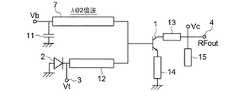
図1は、本発明の実施の形態1に係るVCOの構成を示した図である。図1においては、直列正帰還構成のVCOを示し、周波数が所望の周波数の整数分の1である電気信号(すなわち基本波信号)を発振させて高調波信号を出力端子から取り出す、高調波取り出し型発振器を示す。1はトランジスタ、2はバラクタ、3は制御電圧端子、4は信号の出力端子、5は2倍波信号の波長の四分の一に相当する長さの先端開放スタブ、12および13は線路、14はエミッタ線路、15は基本波反射スタブ、16はバイアス電圧端子である。バラクタ2、線路12および制御電圧端子3は、バラクタ2の電圧可変な容量成分と線路12のインダクタンス成分により可変共振器を構成している。制御電圧端子3に印加する制御電圧Vtを変化させる事で出力周波数を変化させる事が可能となる。先端開放スタブ5は、上記可変共振器に並列に接続される。エミッタ線路14はトランジスタ1のエミッタとグラウンドの間に接続される。基本波反射スタブ15は、例えば回路内部で発振する基本波の波長の4分の1に相当する先端開放スタブであり、図1に示すようにトランジスタの出力側に取り付けられた線路13に接続されている。
FIG. 1 is a diagram showing a configuration of a VCO according to
このVCO回路の構造は、例えばMMICであり、またMIC(マイクロ波集積回路)やディクスリート素子を用いたものであってもよい。基板としては、GaAs(砒化ガリウム)、GaN(窒化ガリウム)、InP(リン化インジウム)、Si等の材料を使用しても良い。
トランジスタ1の材料に制限は無く、シリコン、砒化ガリウム、窒化ガリウム等が使用可能である。トランジスタ1の構造にも制限は無く、バイポーラトランジスタ、電界効果トランジスタ、高電子移動度トランジスタ等が使用可能であり、真空管であっても良い。The structure of the VCO circuit is, for example, an MMIC, and may be one using a MIC (microwave integrated circuit) or a discrete component. As the substrate, a material such as GaAs (gallium arsenide), GaN (gallium nitride), InP (indium phosphide), or Si may be used.
The material of the
次に動作を説明する。回路内部の熱雑音等の雑音信号はトランジスタ1に入力されて増幅された後、トランジスタ1のエミッタ線路14からの帰還または基本波反射スタブ15からの反射によって線路13およびトランジスタ1を経てトランジスタ1のベース側に戻り、再びトランジスタ1に入力されて増幅される。このようにしてVCO内部で基本波周波数における発振が生じるが、トランジスタ1は基本波周波数の2倍、3倍、・・・の周波数の高調波信号(2倍波信号、3倍波信号、・・・)も発生してしまう。基本波反射スタブ15が2倍波信号に対しては開放であるため、2倍波信号は出力端子4へと向かい発振器の外部へ出力される。基本波信号は基本波反射スタブ15よりも出力側に進行しないため、発振器の外部へは出力されない。 Next, the operation will be described. A noise signal such as a thermal noise inside the circuit is inputted to the
もし、これらの高調波信号が制御電圧端子4まで伝播し、制御電圧Vtを変動させてしまうと、意図せずに出力周波数が変動してしまう。すなわち出力周波数の安定性が損なわれ位相雑音の増加となる。この制御電圧Vtの変動を抑制するために基本波信号は通過させ、高調波信号は吸収する先端開放スタブ5をトランジスタ1と線路12との間に追加している。この先端開放スタブ5によって高調波信号は制御電圧端子3に伝播できなくなる。一方で基本波信号はバラクタ2へ伝播するため、外部から制御電圧Vtを変化させた際におけるバラクタ2の容量変化により、発振周波数を変化させる事が可能である。 If these harmonic signals propagate to the
本実施の形態では、先端開放スタブ5は2倍波信号の波長の四分の一に相当する長さとしたため、基本波周波数において先端開放スタブ5は非短絡かつ非開放の負荷を有し、トランジスタ1のエミッタ線路14からの帰還または基本波反射スタブ15からの反射により戻ってきた基本波信号は先端開放スタブ5およびバラクタ2の両者へ伝播する。このため、基本波に対して複数のスタブを使用した共振器が構成され、基本波に対して高いQ値を実現できる。このとき基本波と高調波は発振器において6dB/octの関係にあるので基本波と高調波の両方の位相雑音を低減することができる。一方、2倍波周波数において先端開放スタブ5は短絡負荷を有し、2倍波信号は全て先端開放スタブ5へと伝播するため、バラクタ2に2倍波信号が伝播しない。このため、2倍波信号による制御電圧Vtの変動は抑制され、バラクタ2を有する可変共振回路で発生する位相雑音が低減される。また、先端開放スタブ5の接続箇所では2倍波信号による電界変動が生じないため、2倍波信号によるトランジスタ1のベース電圧の変動が抑制され、さらに位相雑音が低減される。以上から低位相雑音のVCOを実現する事ができる。 In the present embodiment, since the
図1では、先端開放スタブ5の線路長は一例として2倍波信号の波長の四分の一としたが、2倍波信号の波長の四分の一に2倍波信号の半波長の整数倍を加算した長さとしてもよい。すなわち、2倍波信号の波長をλとすると、下記の(1)式で定義される長さ(2倍波信号の波長の四分の一の奇数倍)とすればよい。(1)式で定義される長さに相当する先端開放スタブは、高調波に対して短絡負荷を有し、基本波に対して非短絡かつ非開放の負荷を有するからである。 In FIG. 1, the line length of the open-ended

また、先端開放スタブ5の長さを厳密に上記の(1)式の長さに設定する必要はなく、±λ/16程度の誤差を有していてもよい。この誤差範囲内であれば、共振回路側の2倍波負荷インピーダンスに対する位相雑音の大きさの計算結果より、厳密に(1)式の長さに設定した場合の位相雑音と比べて0.8dBないし1.4dB程度の悪化に留まり、位相雑音の抑制効果が十分に期待できるからである。 Further, it is not necessary to strictly set the length of the
本実施の形態では、高調波信号を2倍波信号としたが、3倍波信号、4倍波信号、・・・が位相雑音の支配的な劣化要因となる場合であれば、3倍波周波数、4倍波周波数、・・・において短絡負荷となるよう3倍波信号、4倍波信号、・・・の波長λに対して(1)式を満たす線路長にした先端開放スタブを使用する事も可能である。その際も±λ/16の誤差を有しても位相雑音の抑制効果が期待できる。 In the present embodiment, the harmonic signal is a second harmonic signal. However, if the third harmonic signal, the fourth harmonic signal,... Uses an open-ended stub with a line length satisfying the formula (1) for the wavelength λ of the third harmonic signal, the fourth harmonic signal,. It is also possible to do. At this time, even if there is an error of ± λ / 16, the effect of suppressing the phase noise can be expected.
なお、図1の例では、先端開放スタブ5を1つだけ可変共振器に並列接続した例を示したが、それに制限されることなく、2以上の先端開放スタブ5を可変共振器に並列接続するようにしてもよい。 In the example of FIG. 1, an example is shown in which only one open-ended
以上のように、本実施の形態においては、長くとも高調波信号の波長の四分の一の奇数倍に高調波信号の波長の十六分の一を加算した長さであり、短くとも高調波信号の波長の四分の一の奇数倍に高調波信号の波長の十六分の一を減算した長さの先端開放スタブ5を1以上可変共振器に並列接続するようにした。上記先端開放スタブ5は基本波周波数において非短絡かつ非開放の負荷を有し、かつ、高調波周波数において短絡の負荷を有するので、基本波周波数においては、基本波信号は先端開放スタブ5およびバラクタ2の両者へ伝播する。すなわち複数のスタブを使用した共振器が構成され、高いQ値を実現できる。一方、高調波周波数においては、先端開放スタブ5は短絡負荷を有し、高調波信号は全て先端開放スタブ5へと伝播するため、バラクタ2に高調波信号が伝播せず、高調波信号による制御電圧Vtの変動が抑制される。また、先端開放スタブ5の接続箇所では高調波信号による電界変動が生じないため、高調波信号によるトランジスタ1のベース電圧の変動が抑制される。以上から、本実施の形態においては、基本波周波数におけるQ値を向上させ、かつ、バラクタおよびトランジスタに印加される電圧の高調波信号による変動を抑制することができるため、位相雑音の低いVCOを実現する事ができる。 As described above, in the present embodiment, the length is a length obtained by adding one-sixth of the wavelength of the harmonic signal to an odd multiple of one-fourth of the wavelength of the harmonic signal. One or more open-ended
なお、図1においては基本波反射スタブ15を有する高調波取り出し型発振器の例を示したが、基本波反射スタブ15を有さず基本波を出力する基本波発振器であっても、同様に位相雑音の低いVCOを実現する事ができる。また、上記可変共振器がトランジスタ1のエミッタ側またはコレクタ側に接続されているVCOにおいても、先端開放スタブ5が上記可変共振器に並列に接続されていれば、同様に位相雑音の低いVCOを実現することができる。 Although FIG. 1 shows an example of a harmonic extraction type oscillator having a fundamental
本実施の形態では、基本波信号または高調波信号の周波数が1GHz未満であっても、先端開放スタブ5の線路長を(1)式で表される長さとすることができれば、上記と同様の効果を奏する。また、図1において可変共振器はバラクタ1と線路12を有する構成としたが、バラクタを含むLCR回路によって構成されていてもよい。 In the present embodiment, even if the frequency of the fundamental wave signal or the harmonic signal is less than 1 GHz, if the line length of the open-ended
実施の形態2.
図2は、本発明の実施の形態2に係るVCOの構成を示した図である。図2において、1〜4および12〜16は、図1と同様であり、6は2倍波信号の波長に相当する長さの先端短絡スタブである。2倍波周波数において短絡負荷を有する可変共振器と並列に接続するスタブは先端短絡スタブを用いても実現可能であり、2倍波信号の波長λに対して、下記の(2)式で示される線路長(2倍波信号の波長の整数倍)とすれば良い。
FIG. 2 is a diagram showing a configuration of the VCO according to the second embodiment of the present invention. 2, 1 to 4 and 12 to 16 are the same as those in FIG. 1, and 6 is a tip short-circuited stub having a length corresponding to the wavelength of the second harmonic signal. A stub connected in parallel with a variable resonator having a short-circuit load at the second harmonic frequency can also be realized using a tip short-circuit stub, and is expressed by the following equation (2) with respect to the wavelength λ of the second harmonic signal. The line length (the integral multiple of the wavelength of the second harmonic signal) may be used.
おおむね1GHz未満の低い周波数では(2)式で表される線路長の先端短絡スタブ6は基本波周波数においても短絡負荷となる。このため、バラクタ2を含む可変共振器に基本波信号が伝播しなくなってしまい、発振周波数を変化させる事ができなくなる。一方、高周波数になるにつれて先端短絡スタブ6の線路に含まれる寄生C成分や寄生L成分によって(2)式で表される線路長は基本波信号の半波長の整数倍ではなくなるため、(2)式の線路長の先端短絡スタブ6は基本波周波数において非短絡かつ非開放の負荷を有するようになる。したがって、おおむね1GHz以上の基本波周波数で発振するVCOでは、実施の形態1の先端開放スタブ5の代わりに、(2)式で表される線路長の先端短絡スタブ6を使用することができる。 In general, at a low frequency of less than 1 GHz, the tip short-circuited
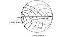
本実施の形態に係るVCOの動作原理は、実施の形態1に係るVCOと基本的に同様である。本実施の形態に係るVCOの動作を確認すべく、回路構造をMMICとして38GHz基本波信号および76GHzの2倍波信号がトランジスタベース端子から図2中の点線枠内へ入力された際の、図2中の点線枠内の電界分布を計算した一例を図3および図4にそれぞれ示す。この計算は先端短絡スタブ6の中間にバイアス電圧端子16を接続した配置で行っているが、図2に示すVCOと本質的な違いはない。
図3に示された電界分布から38GHz基本波信号は先端短絡スタブ6およびバラクタ2の両者へ伝播する事がわかる。一方、図4に示された電界分布から76GHzの2倍波信号は先端短絡スタブ6のみへ伝播し、バラクタ2へは伝播しない事がわかる。さらに、トランジスタベース端子では76GHzの2倍波信号による電界はゼロになる、すなわち、ベース電圧が変動しないことがわかる。The operating principle of the VCO according to the present embodiment is basically the same as that of the VCO according to the first embodiment. In order to confirm the operation of the VCO according to the present embodiment, when the circuit structure is MMIC, a 38 GHz fundamental wave signal and a 76 GHz double wave signal are input from the transistor base terminal into the dotted frame in FIG. An example in which the electric field distribution in the dotted line frame in Fig. 2 is calculated is shown in Figs. This calculation is performed with an arrangement in which the
It can be seen from the electric field distribution shown in FIG. 3 that the 38 GHz fundamental wave signal propagates to both the tip
表1に実施の形態2に係るVCOの位相雑音の計算結果の一例を示す。表1の結果から、先端短絡スタブ6を設置していない場合と設置した場合とで出力周波数に大きな変動はなく、先端短絡スタブ6を追加する事で位相雑音が抑圧される事がわかる。また、制御電圧端子3に加える電圧によって共に約1GHzの周波数変化が可能である。 Table 1 shows an example of the calculation result of the phase noise of the VCO according to the second embodiment. From the results in Table 1, it can be seen that there is no significant fluctuation in the output frequency between the case where the tip short-
なお、本実施の形態においても、実施の形態1と同様、先端短絡スタブ6を厳密に(2)式の長さに設定する必要はなく、±λ/16の誤差を有しても位相雑音の抑制効果が期待できる。図5に先端短絡スタブ6の長さをλ−λ/16、λ−λ/32、λ、λ+λ/32、λ+λ/16とした場合における、トランジスタ1のベース側から見た共振回路側(可変共振回路および先端短絡スタブ6)の2倍波負荷インピーダンスを50Ωのスミスチャートにドットで示す。また、共振回路側の2倍波負荷インピーダンスに対する位相雑音の大きさの計算結果をスミスチャート上の0.2dBステップの等高線で示している。先端短絡スタブ6の長さがλである場合に、位相雑音が最も抑制される最適点、すなわちスミスチャートの左端、をとる。長さがλからずれるに従って、共振回路側のインピーダンスはスミスチャートの外周上を移動し、位相雑音が劣化していくことが分かる。計算結果より、先端短絡スタブ6の長さがλ±λ/16となったときは、位相雑音は最適点より0.8dBないし1.4dB程度劣化することが分かるが、この場合においても十分に位相雑音の抑制効果が期待できる。先端開放スタブ5を用いた実施の形態1においても、共振回路側の2倍波負荷インピーダンスに対する位相雑音の大きさの計算結果は図5と同様である。
また、3倍波周波数、4倍波周波数、・・・において短絡負荷となるよう線路長を3倍波信号、4倍波信号、・・・の波長に対して(2)式を満たすようにした先端短絡スタブを使用する事も可能である。その際も±λ/16の誤差を有しても位相雑音の抑制効果が期待できる。In the present embodiment as well, as in the first embodiment, it is not necessary to strictly set the tip short-
Also, the line length is set to satisfy the equation (2) with respect to the wavelength of the third harmonic signal, the fourth harmonic signal,. It is also possible to use a shorted tip short stub. At this time, even if there is an error of ± λ / 16, the effect of suppressing the phase noise can be expected.
なお、図2の例では、先端短絡スタブ6を1つだけ可変共振器に並列接続した例を示したが、それに制限されることなく、2以上の先端短絡スタブ6を可変共振器に並列接続するようにしてもよい。また、先端短絡スタブ6の先端は、MIM(Metal−Insulator−Metal)キャパシタを一例とする容量を介して高周波のみグラウンドに短絡するようにしてもよい。 In the example of FIG. 2, an example in which only one short-circuited
本実施の形態においては、長くとも高調波信号の波長の整数倍に高調波信号の波長の十六分の一を加算した長さであり、短くとも高調波信号の波長の整数倍に高調波信号の波長の十六分の一を減算した長さの先端短絡スタブを1以上可変共振器に並列接続するようにした。上記先端短絡スタブ6は基本波周波数において非短絡かつ非開放の負荷を有し、かつ、高調波周波数において短絡の負荷を有するので基本波周波数においては、先端短絡スタブ6およびバラクタ2の両者へ伝播する。すなわち複数のスタブを使用した共振器が構成され、高いQ値を実現できる。一方、高調波周波数においては、先端開放スタブ5は短絡負荷を有し、高調波信号は全て先端短絡スタブ6へと伝播するため、バラクタ2に高調波信号が伝播せず、高調波信号による制御電圧Vtの変動が抑制される。また、先端短絡スタブ6の接続箇所では高調波信号による電界変動が生じないため、高調波信号によるトランジスタ1のベース電圧の変動が抑制される。以上から、本実施の形態においても、実施の形態1と同様に、低位相雑音のVCOを実現する事ができる。 In the present embodiment, it is a length obtained by adding one-sixteenth of the wavelength of the harmonic signal to the integral multiple of the wavelength of the harmonic signal at the longest, and the harmonics at least an integral multiple of the wavelength of the harmonic signal. One or more tip short-circuited stubs having a length obtained by subtracting one-sixteenth of the signal wavelength are connected in parallel to the variable resonator. The tip short-circuited
なお、図2においては基本波反射スタブ15を有する高調波取り出し型発振器の例を示したが、基本波反射スタブ15を有さず基本波を出力する基本波発振器であっても、同様に位相雑音の低いVCOを実現する事ができる。また、可変共振器がトランジスタ1のエミッタ側またはコレクタ側に接続されているVCOにおいても、先端短絡スタブ6が上記可変共振器に並列に接続されていれば、同様に位相雑音の低いVCOを実現することができる。 In FIG. 2, an example of a harmonic extraction type oscillator having a fundamental
図2において可変共振器はバラクタ1と線路12を有する構成としたが、バラクタを含むLCR回路によって構成されていてもよい。 In FIG. 2, the variable resonator has the
実施の形態3.
図6は、本発明の実施の形態3に係るVCOの構成を示した図である。図6において、1〜4および12〜15は、図1と同様であり、7は、接続箇所から容量(キャパシタ)11を介した高周波短絡箇所までの線路長が、2倍波信号の波長に相当する長さであるバイアス回路である。
FIG. 6 is a diagram showing a configuration of the VCO according to the third embodiment of the present invention. In FIG. 6, 1 to 4 and 12 to 15 are the same as those in FIG. 1, and 7 indicates that the line length from the connection location to the high frequency short-circuit location via the capacitor (capacitor) 11 is the wavelength of the second harmonic signal. This is a bias circuit having a corresponding length.
上述の実施の形態2で説明したように先端短絡スタブ6を新たに追加せずとも、バイアス回路において、接続箇所から上述の(2)式を満たす距離だけ離れた箇所に容量11を介して短絡とする事で、上述の実施の形態2の先端短絡スタブの追加と同様の効果が得られる。 As described in the above-described second embodiment, the
なお、上記の説明においては、バイアス回路7の線路長を2倍波信号の波長に相当する長さとして説明したが、その場合に限らず、バイアス回路7の線路長は2倍波信号の波長の整数倍に相当する長さにすればよい。また、2倍波信号に限らず3倍波以上の高調波の波長の整数倍に相当する長さとしてもよい。 In the above description, the line length of the bias circuit 7 is described as the length corresponding to the wavelength of the second harmonic signal. However, the line length of the bias circuit 7 is not limited to the wavelength of the second harmonic signal. It may be a length corresponding to an integral multiple of. Further, the length is not limited to the second harmonic signal, and may be a length corresponding to an integral multiple of the wavelength of the third or higher harmonic.
また、バイアス回路7の線路長が±λ/16の誤差を有しても位相雑音の抑制効果が期待できる。 Even if the line length of the bias circuit 7 has an error of ± λ / 16, the effect of suppressing the phase noise can be expected.
以上のように、本実施の形態においては、バイアス回路接続箇所からキャパシタを介した接地箇所までの線路長が、長くとも高調波信号の波長の整数倍に高調波信号の波長の十六分の一を加算した長さであり、短くとも高調波信号の波長の整数倍に高調波信号の波長の十六分の一を減算した長さを有するバイアス回路を、可変共振器に並列に接続するようにしたので、実施の形態2と同様に、本実施の形態においても、低位相雑音のVCOを実現する事ができる。 As described above, in the present embodiment, the line length from the bias circuit connecting point to the grounded point through the capacitor is at least sixteen times the wavelength of the harmonic signal at an integral multiple of the wavelength of the harmonic signal. Connect a bias circuit in parallel to the variable resonator, which is a length that is one plus one, and has a length that is at least sixteen times the wavelength of the harmonic signal minus an integral multiple of the wavelength of the harmonic signal. As described above, similarly to the second embodiment, a VCO with low phase noise can also be realized in this embodiment.
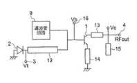
実施の形態4.
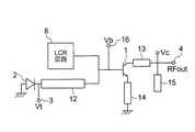
図7は、本発明の実施の形態4に係るVCOの構成を示した図である。図7において、1〜4および12〜16は、図1と同様であり、8は2倍波周波数において短絡負荷を有するLCR回路である。
FIG. 7 is a diagram showing a configuration of the VCO according to the fourth embodiment of the present invention. 7, 1 to 4 and 12 to 16 are the same as those in FIG. 1, and 8 is an LCR circuit having a short-circuit load at the second harmonic frequency.
また、図8は、本発明の実施の形態4に係るVCOの構成の他の例を示した図である。図8において、1〜4および12〜16は、図1と同様であり、9は2倍波周波数において短絡負荷を有する導波管回路である。 FIG. 8 is a diagram showing another example of the configuration of the VCO according to the fourth embodiment of the present invention. 8, 1 to 4 and 12 to 16 are the same as those in FIG. 1, and 9 is a waveguide circuit having a short-circuit load at the second harmonic frequency.
なお、LCR回路8および導波管回路9は、いずれも、高調波信号の周波数において短絡負荷または短絡負荷に近い例えば−30jΩ以上+30jΩ以下の範囲の負荷であるものとする。この範囲の負荷は、特性インピーダンスが50Ωの系では実施の形態2の先端短絡スタブ6に対応させるとλ±λ/16の範囲に相当し、図5からも分かるように、位相雑音は最適点から0.8dBないし1.4dB程度の劣化で収まるため、位相雑音を抑える効果がある。また、図5のスミスチャートから分かるように、インピーダンスが上記の虚数成分に加えて0Ω以上15Ω以下の実数成分を有していたとしても、位相雑音は最適点から0.8dBないし1.4dB程度の劣化で収まり、位相雑音を抑える効果がある。 Note that both the
上述の実施の形態1または2で追加した回路は、基本波周波数において非短絡かつ非開放の負荷、高調波周波数において短絡負荷を有すれば良く、線路スタブである必要は無い。従って、本実施の形態に示すように、LCR回路8や導波管回路9も使用する事が可能である。 The circuit added in the first or second embodiment described above may have a non-shorted and non-open load at the fundamental frequency and a short-circuit load at the harmonic frequency, and does not need to be a line stub. Therefore, as shown in this embodiment, the
以上のように、本実施の形態においては、基本周波数に対しては短絡ではなく、かつ、高調波信号の周波数において実数成分が0Ω以上15Ω以下かつ虚数成分が−30jΩ以上+30jΩ以下の負荷を有するLCR回路8または導波管回路9を、少なくとも1つ、可変共振器に並列に接続するようにしたので、上述の実施の形態2または3と同様に、低位相雑音のVCOを実現する事ができる。 As described above, the present embodiment is not short-circuited with respect to the fundamental frequency, and has a load whose real component is 0Ω or more and 15Ω or less and whose imaginary component is −30 jΩ or more and +30 jΩ or less at the frequency of the harmonic signal. Since at least one
実施の形態5.
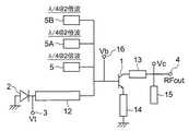
上述の実施の形態1、2、4で追加した回路は、図9のように、複数追加する事も可能である。図9では、実施の形態1で示した2倍波信号の波長の四分の一に相当する長さの先端開放スタブ5、5A、5Bを3個接続した例を示しているが、実施の形態2で示した先端短絡スタブ6にしてもよいし、実施の形態4で示したLCR回路8や導波管回路9にしてもよい。また、個数も3個に限らず、適宜、任意の個数を設けるようにしてもよい。
A plurality of circuits added in the first, second, and fourth embodiments can be added as shown in FIG. FIG. 9 shows an example in which three
また、複数の次数の高調波信号が位相雑音の劣化要因となるのであれば、図10のように、複数追加した回路をそれぞれ異なる次数の高調波信号に対して短絡負荷とする事も可能である。図10の例では、実施の形態1で示した3倍波信号の波長の四分の一に相当する長さの先端開放スタブ5と、3倍波信号の波長の四分の一に相当する長さの先端開放スタブ5Cと、4倍波信号の波長の四分の一に相当する長さの先端開放スタブ5Dとが追加されているが、これは一例であり、これらに限定されるものではない。位相雑音の劣化要因に基づいて、適宜、組み合わせを選択する。 In addition, if a plurality of higher-order harmonic signals cause deterioration of phase noise, it is possible to use a plurality of added circuits as short-circuit loads for different-order harmonic signals as shown in FIG. is there. In the example of FIG. 10, the tip
さらに、図11のように、複数追加する回路は、先端短絡スタブ、先端開放スタブ、LCR回路、導波管回路と異なっていても良い。図11の例では、4倍波信号の波長に相当する長さの先端短絡スタブ6Aと、3倍波信号の波長の四分の一に相当する長さの先端開放スタブ5Eと、実施の形態2で示した2倍波信号の波長に相当する長さの先端短絡スタブ6とが設けられているが、これに限定されるものではない。これについても、位相雑音の劣化要因に基づいて、適宜、組み合わせを選択する。 Furthermore, as shown in FIG. 11, a plurality of additional circuits may be different from the tip short-circuit stub, the tip open stub, the LCR circuit, and the waveguide circuit. In the example of FIG. 11, the tip short-
以上のように、本実施の形態においても、上述の実施の形態1、2、4と同様に、低位相雑音のVCOを実現する事ができる。 As described above, also in the present embodiment, a low phase noise VCO can be realized as in the first, second, and fourth embodiments.
実施の形態6.
図12は、実施の形態1から5に係る電圧制御発振器を備えた高周波無線装置の構成例である。高周波無線装置20はレーダーや携帯電話等であり、マイクロ波やミリ波を使って送信または受信あるいはその両方を行う装置である。
周波数制御装置21からの電圧信号による周波数で電圧制御発振器22が発振し、増幅器23で発振信号が増幅され、出力アンテナ24からマイクロ波またはミリ波が送信される。受信アンテナ25でマイクロ波またはミリ波を受信し、周波数制御装置26の電圧信号に基づいて電圧制御発振器27が出力する発振信号と受信アンテナ25からの受信信号をミキサ28で周波数変換して所望の信号を出力する。
送信アンテナ24と受信アンテナ25は一体としてもよい。周波数制御装置21と26、電圧制御発振器22と27はそれぞれ一体としてもよい。また、送信部分と受信部分の一方にのみ実施の形態1から5に係る電圧制御発振器を使用することでもよい。
高周波無線装置が実施の形態1から5に係る電圧制御発振器を用いることで、位相雑音の少ない高品質なマイクロ波またはミリ波を送信することができる。また受信時の雑音を低減することができる。
FIG. 12 is a configuration example of a high-frequency radio apparatus including the voltage controlled oscillator according to the first to fifth embodiments. The high-
The voltage controlled
The
By using the voltage controlled oscillator according to
1 トランジスタ、2 バラクタ、3 制御電圧端子、4 出力端子、5 先端開放スタブ、6 先端短絡スタブ、7 バイアス回路、8 LCR回路、9 導波管回路、20 高周波無線装置。 1 transistor, 2 varactor, 3 control voltage terminal, 4 output terminal, 5 tip open stub, 6 tip short circuit stub, 7 bias circuit, 8 LCR circuit, 9 waveguide circuit, 20 high frequency radio equipment.
Claims (7)
Translated fromJapanese長くとも高調波信号の波長の四分の一の奇数倍に高調波信号の波長の十六分の一を加算した長さであり、短くとも高調波信号の波長の四分の一の奇数倍に高調波信号の波長の十六分の一を減算した長さを有する先端開放スタブを、少なくとも1つ、前記可変共振器に並列に接続したことを特徴とする電圧制御発振器。A voltage-controlled oscillator having a variable resonator,
The length of the harmonic signal is an odd multiple of one quarter of the wavelength of the harmonic signal plus one-sixteenth of the wavelength of the harmonic signal, and at least an odd multiple of one quarter of the wavelength of the harmonic signal. A voltage-controlled oscillator comprising: at least one open-ended stub having a length obtained by subtracting one-sixteenth of the wavelength of a harmonic signal in parallel with the variable resonator.
長くとも高調波信号の波長の整数倍に高調波信号の波長の十六分の一を加算した長さであり、短くとも高調波信号の波長の整数倍に高調波信号の波長の十六分の一を減算した長さを有する先端短絡スタブを、少なくとも1つ、前記可変共振器に並列に接続したことを特徴とする電圧制御発振器。A voltage-controlled oscillator having a variable resonator,
It is the length obtained by adding one-tenth of the wavelength of the harmonic signal to the integer multiple of the wavelength of the harmonic signal at the longest, and sixteenths of the wavelength of the harmonic signal at least an integral multiple of the wavelength of the harmonic signal. A voltage-controlled oscillator comprising at least one short-circuited short-circuited stub having a length obtained by subtracting one of the variable resonators in parallel.
バイアス回路接続箇所からキャパシタを介した接地箇所までの線路長が、長くとも高調波信号の波長の整数倍に高調波信号の波長の十六分の一を加算した長さであり、短くとも高調波信号の波長の整数倍に高調波信号の波長の十六分の一を減算した長さを有するバイアス回路を、前記可変共振器に並列に接続したことを特徴とする電圧制御発振器。A voltage-controlled oscillator having a variable resonator,
The line length from the bias circuit connection point to the ground point via the capacitor is a length obtained by adding an integral multiple of the wavelength of the harmonic signal to one-sixth of the wavelength of the harmonic signal. A voltage-controlled oscillator comprising: a bias circuit having a length obtained by subtracting one-sixteenth of a wavelength of a harmonic signal by an integral multiple of a wavelength of a wave signal;
発振周波数に対しては短絡ではなく、高調波信号の周波数において、実数成分が0Ω以上15Ω以下、かつ、虚数成分が−30jΩ以上+30jΩ以下の負荷を有するLCR回路を、少なくとも1つ、前記可変共振器に並列に接続したことを特徴とする電圧制御発振器。A voltage-controlled oscillator having a variable resonator,
At least one LCR circuit having a load whose real component is 0Ω or more and 15Ω or less and whose imaginary component is −30 jΩ or more and +30 jΩ or less at the frequency of the harmonic signal, not a short circuit with respect to the oscillation frequency, is the variable resonance. A voltage-controlled oscillator characterized by being connected in parallel to a vessel.
発振周波数に対しては短絡ではなく、高調波信号の周波数において、実数成分が0Ω以上15Ω以下、かつ、虚数成分が−30jΩ以上+30jΩ以下の負荷を有する導波管回路を、少なくとも1つ、前記可変共振器に並列に接続したことを特徴とする電圧制御発振器。A voltage-controlled oscillator having a variable resonator,
At least one waveguide circuit having a load with a real component of 0Ω to 15Ω and an imaginary component of −30 jΩ to +30 jΩ in the harmonic signal frequency, not a short circuit with respect to the oscillation frequency, A voltage-controlled oscillator characterized by being connected in parallel to a variable resonator.
Priority Applications (4)
| Application Number | Priority Date | Filing Date | Title |
|---|---|---|---|
| JP2008223274AJP2010062614A (en) | 2008-09-01 | 2008-09-01 | Voltage controlled oscillator, mmic, and high frequency radio apparatus |
| US12/473,317US20100052799A1 (en) | 2008-09-01 | 2009-05-28 | Voltage controlled oscillator, mmic, and high frequency wireless device |
| CN200910159440.0ACN101667829B (en) | 2008-09-01 | 2009-06-30 | Voltage controlled oscillator, single-chip microwave integrated circuit and high-frequency wireless apparatus |
| DE102009036098ADE102009036098A1 (en) | 2008-09-01 | 2009-08-04 | Voltage controlled oscillator, MMIC and high frequency radio device |
Applications Claiming Priority (1)
| Application Number | Priority Date | Filing Date | Title |
|---|---|---|---|
| JP2008223274AJP2010062614A (en) | 2008-09-01 | 2008-09-01 | Voltage controlled oscillator, mmic, and high frequency radio apparatus |
Publications (1)
| Publication Number | Publication Date |
|---|---|
| JP2010062614Atrue JP2010062614A (en) | 2010-03-18 |
Family
ID=41693995
Family Applications (1)
| Application Number | Title | Priority Date | Filing Date |
|---|---|---|---|
| JP2008223274APendingJP2010062614A (en) | 2008-09-01 | 2008-09-01 | Voltage controlled oscillator, mmic, and high frequency radio apparatus |
Country Status (4)
| Country | Link |
|---|---|
| US (1) | US20100052799A1 (en) |
| JP (1) | JP2010062614A (en) |
| CN (1) | CN101667829B (en) |
| DE (1) | DE102009036098A1 (en) |
Cited By (2)
| Publication number | Priority date | Publication date | Assignee | Title |
|---|---|---|---|---|
| JP2015094843A (en)* | 2013-11-12 | 2015-05-18 | 株式会社島津製作所 | Laser equipment |
| WO2019073677A1 (en)* | 2017-10-13 | 2019-04-18 | 株式会社ヨコオ | High-frequency module |
Families Citing this family (167)
| Publication number | Priority date | Publication date | Assignee | Title |
|---|---|---|---|---|
| JP5597998B2 (en)* | 2010-01-15 | 2014-10-01 | 三菱電機株式会社 | High frequency double wave oscillator |
| US9113347B2 (en) | 2012-12-05 | 2015-08-18 | At&T Intellectual Property I, Lp | Backhaul link for distributed antenna system |
| US10009065B2 (en) | 2012-12-05 | 2018-06-26 | At&T Intellectual Property I, L.P. | Backhaul link for distributed antenna system |
| US9525524B2 (en) | 2013-05-31 | 2016-12-20 | At&T Intellectual Property I, L.P. | Remote distributed antenna system |
| US9999038B2 (en) | 2013-05-31 | 2018-06-12 | At&T Intellectual Property I, L.P. | Remote distributed antenna system |
| US8897697B1 (en) | 2013-11-06 | 2014-11-25 | At&T Intellectual Property I, Lp | Millimeter-wave surface-wave communications |
| US9209902B2 (en) | 2013-12-10 | 2015-12-08 | At&T Intellectual Property I, L.P. | Quasi-optical coupler |
| CN104079269B (en)* | 2014-05-30 | 2016-08-17 | 中国电子科技集团公司第十研究所 | Microwave VCO directly modulation High Linear FM signal generation circuit |
| US9692101B2 (en) | 2014-08-26 | 2017-06-27 | At&T Intellectual Property I, L.P. | Guided wave couplers for coupling electromagnetic waves between a waveguide surface and a surface of a wire |
| US9768833B2 (en) | 2014-09-15 | 2017-09-19 | At&T Intellectual Property I, L.P. | Method and apparatus for sensing a condition in a transmission medium of electromagnetic waves |
| US10063280B2 (en) | 2014-09-17 | 2018-08-28 | At&T Intellectual Property I, L.P. | Monitoring and mitigating conditions in a communication network |
| US9628854B2 (en) | 2014-09-29 | 2017-04-18 | At&T Intellectual Property I, L.P. | Method and apparatus for distributing content in a communication network |
| US9615269B2 (en) | 2014-10-02 | 2017-04-04 | At&T Intellectual Property I, L.P. | Method and apparatus that provides fault tolerance in a communication network |
| US9685992B2 (en) | 2014-10-03 | 2017-06-20 | At&T Intellectual Property I, L.P. | Circuit panel network and methods thereof |
| US9503189B2 (en) | 2014-10-10 | 2016-11-22 | At&T Intellectual Property I, L.P. | Method and apparatus for arranging communication sessions in a communication system |
| US9973299B2 (en) | 2014-10-14 | 2018-05-15 | At&T Intellectual Property I, L.P. | Method and apparatus for adjusting a mode of communication in a communication network |
| US9762289B2 (en) | 2014-10-14 | 2017-09-12 | At&T Intellectual Property I, L.P. | Method and apparatus for transmitting or receiving signals in a transportation system |
| US9564947B2 (en) | 2014-10-21 | 2017-02-07 | At&T Intellectual Property I, L.P. | Guided-wave transmission device with diversity and methods for use therewith |
| US9520945B2 (en) | 2014-10-21 | 2016-12-13 | At&T Intellectual Property I, L.P. | Apparatus for providing communication services and methods thereof |
| US9653770B2 (en) | 2014-10-21 | 2017-05-16 | At&T Intellectual Property I, L.P. | Guided wave coupler, coupling module and methods for use therewith |
| US9627768B2 (en) | 2014-10-21 | 2017-04-18 | At&T Intellectual Property I, L.P. | Guided-wave transmission device with non-fundamental mode propagation and methods for use therewith |
| US9769020B2 (en) | 2014-10-21 | 2017-09-19 | At&T Intellectual Property I, L.P. | Method and apparatus for responding to events affecting communications in a communication network |
| US9780834B2 (en) | 2014-10-21 | 2017-10-03 | At&T Intellectual Property I, L.P. | Method and apparatus for transmitting electromagnetic waves |
| US9312919B1 (en) | 2014-10-21 | 2016-04-12 | At&T Intellectual Property I, Lp | Transmission device with impairment compensation and methods for use therewith |
| US9577306B2 (en) | 2014-10-21 | 2017-02-21 | At&T Intellectual Property I, L.P. | Guided-wave transmission device and methods for use therewith |
| US10009067B2 (en) | 2014-12-04 | 2018-06-26 | At&T Intellectual Property I, L.P. | Method and apparatus for configuring a communication interface |
| US9680670B2 (en) | 2014-11-20 | 2017-06-13 | At&T Intellectual Property I, L.P. | Transmission device with channel equalization and control and methods for use therewith |
| US9954287B2 (en) | 2014-11-20 | 2018-04-24 | At&T Intellectual Property I, L.P. | Apparatus for converting wireless signals and electromagnetic waves and methods thereof |
| US9800327B2 (en) | 2014-11-20 | 2017-10-24 | At&T Intellectual Property I, L.P. | Apparatus for controlling operations of a communication device and methods thereof |
| US10340573B2 (en) | 2016-10-26 | 2019-07-02 | At&T Intellectual Property I, L.P. | Launcher with cylindrical coupling device and methods for use therewith |
| US9544006B2 (en) | 2014-11-20 | 2017-01-10 | At&T Intellectual Property I, L.P. | Transmission device with mode division multiplexing and methods for use therewith |
| US9997819B2 (en) | 2015-06-09 | 2018-06-12 | At&T Intellectual Property I, L.P. | Transmission medium and method for facilitating propagation of electromagnetic waves via a core |
| US9461706B1 (en) | 2015-07-31 | 2016-10-04 | At&T Intellectual Property I, Lp | Method and apparatus for exchanging communication signals |
| US9742462B2 (en) | 2014-12-04 | 2017-08-22 | At&T Intellectual Property I, L.P. | Transmission medium and communication interfaces and methods for use therewith |
| US9654173B2 (en) | 2014-11-20 | 2017-05-16 | At&T Intellectual Property I, L.P. | Apparatus for powering a communication device and methods thereof |
| US10243784B2 (en) | 2014-11-20 | 2019-03-26 | At&T Intellectual Property I, L.P. | System for generating topology information and methods thereof |
| US10144036B2 (en) | 2015-01-30 | 2018-12-04 | At&T Intellectual Property I, L.P. | Method and apparatus for mitigating interference affecting a propagation of electromagnetic waves guided by a transmission medium |
| US9876570B2 (en) | 2015-02-20 | 2018-01-23 | At&T Intellectual Property I, Lp | Guided-wave transmission device with non-fundamental mode propagation and methods for use therewith |
| US9749013B2 (en) | 2015-03-17 | 2017-08-29 | At&T Intellectual Property I, L.P. | Method and apparatus for reducing attenuation of electromagnetic waves guided by a transmission medium |
| US10224981B2 (en) | 2015-04-24 | 2019-03-05 | At&T Intellectual Property I, Lp | Passive electrical coupling device and methods for use therewith |
| US9705561B2 (en) | 2015-04-24 | 2017-07-11 | At&T Intellectual Property I, L.P. | Directional coupling device and methods for use therewith |
| US9793954B2 (en) | 2015-04-28 | 2017-10-17 | At&T Intellectual Property I, L.P. | Magnetic coupling device and methods for use therewith |
| US9948354B2 (en) | 2015-04-28 | 2018-04-17 | At&T Intellectual Property I, L.P. | Magnetic coupling device with reflective plate and methods for use therewith |
| US9490869B1 (en) | 2015-05-14 | 2016-11-08 | At&T Intellectual Property I, L.P. | Transmission medium having multiple cores and methods for use therewith |
| US9748626B2 (en) | 2015-05-14 | 2017-08-29 | At&T Intellectual Property I, L.P. | Plurality of cables having different cross-sectional shapes which are bundled together to form a transmission medium |
| US9871282B2 (en) | 2015-05-14 | 2018-01-16 | At&T Intellectual Property I, L.P. | At least one transmission medium having a dielectric surface that is covered at least in part by a second dielectric |
| US10650940B2 (en) | 2015-05-15 | 2020-05-12 | At&T Intellectual Property I, L.P. | Transmission medium having a conductive material and methods for use therewith |
| US10679767B2 (en) | 2015-05-15 | 2020-06-09 | At&T Intellectual Property I, L.P. | Transmission medium having a conductive material and methods for use therewith |
| US9917341B2 (en) | 2015-05-27 | 2018-03-13 | At&T Intellectual Property I, L.P. | Apparatus and method for launching electromagnetic waves and for modifying radial dimensions of the propagating electromagnetic waves |
| US10812174B2 (en) | 2015-06-03 | 2020-10-20 | At&T Intellectual Property I, L.P. | Client node device and methods for use therewith |
| US10103801B2 (en) | 2015-06-03 | 2018-10-16 | At&T Intellectual Property I, L.P. | Host node device and methods for use therewith |
| US9866309B2 (en) | 2015-06-03 | 2018-01-09 | At&T Intellectual Property I, Lp | Host node device and methods for use therewith |
| US10348391B2 (en) | 2015-06-03 | 2019-07-09 | At&T Intellectual Property I, L.P. | Client node device with frequency conversion and methods for use therewith |
| US9912381B2 (en) | 2015-06-03 | 2018-03-06 | At&T Intellectual Property I, Lp | Network termination and methods for use therewith |
| US10154493B2 (en) | 2015-06-03 | 2018-12-11 | At&T Intellectual Property I, L.P. | Network termination and methods for use therewith |
| US9913139B2 (en) | 2015-06-09 | 2018-03-06 | At&T Intellectual Property I, L.P. | Signal fingerprinting for authentication of communicating devices |
| US9608692B2 (en) | 2015-06-11 | 2017-03-28 | At&T Intellectual Property I, L.P. | Repeater and methods for use therewith |
| US10142086B2 (en) | 2015-06-11 | 2018-11-27 | At&T Intellectual Property I, L.P. | Repeater and methods for use therewith |
| US9820146B2 (en) | 2015-06-12 | 2017-11-14 | At&T Intellectual Property I, L.P. | Method and apparatus for authentication and identity management of communicating devices |
| US9667317B2 (en) | 2015-06-15 | 2017-05-30 | At&T Intellectual Property I, L.P. | Method and apparatus for providing security using network traffic adjustments |
| US9640850B2 (en) | 2015-06-25 | 2017-05-02 | At&T Intellectual Property I, L.P. | Methods and apparatus for inducing a non-fundamental wave mode on a transmission medium |
| US9509415B1 (en) | 2015-06-25 | 2016-11-29 | At&T Intellectual Property I, L.P. | Methods and apparatus for inducing a fundamental wave mode on a transmission medium |
| US9865911B2 (en) | 2015-06-25 | 2018-01-09 | At&T Intellectual Property I, L.P. | Waveguide system for slot radiating first electromagnetic waves that are combined into a non-fundamental wave mode second electromagnetic wave on a transmission medium |
| US9628116B2 (en) | 2015-07-14 | 2017-04-18 | At&T Intellectual Property I, L.P. | Apparatus and methods for transmitting wireless signals |
| US10320586B2 (en) | 2015-07-14 | 2019-06-11 | At&T Intellectual Property I, L.P. | Apparatus and methods for generating non-interfering electromagnetic waves on an insulated transmission medium |
| US9882257B2 (en) | 2015-07-14 | 2018-01-30 | At&T Intellectual Property I, L.P. | Method and apparatus for launching a wave mode that mitigates interference |
| US9853342B2 (en) | 2015-07-14 | 2017-12-26 | At&T Intellectual Property I, L.P. | Dielectric transmission medium connector and methods for use therewith |
| US10033108B2 (en) | 2015-07-14 | 2018-07-24 | At&T Intellectual Property I, L.P. | Apparatus and methods for generating an electromagnetic wave having a wave mode that mitigates interference |
| US10205655B2 (en) | 2015-07-14 | 2019-02-12 | At&T Intellectual Property I, L.P. | Apparatus and methods for communicating utilizing an antenna array and multiple communication paths |
| US9847566B2 (en) | 2015-07-14 | 2017-12-19 | At&T Intellectual Property I, L.P. | Method and apparatus for adjusting a field of a signal to mitigate interference |
| US10341142B2 (en) | 2015-07-14 | 2019-07-02 | At&T Intellectual Property I, L.P. | Apparatus and methods for generating non-interfering electromagnetic waves on an uninsulated conductor |
| US9722318B2 (en) | 2015-07-14 | 2017-08-01 | At&T Intellectual Property I, L.P. | Method and apparatus for coupling an antenna to a device |
| US10044409B2 (en) | 2015-07-14 | 2018-08-07 | At&T Intellectual Property I, L.P. | Transmission medium and methods for use therewith |
| US9836957B2 (en) | 2015-07-14 | 2017-12-05 | At&T Intellectual Property I, L.P. | Method and apparatus for communicating with premises equipment |
| US10033107B2 (en) | 2015-07-14 | 2018-07-24 | At&T Intellectual Property I, L.P. | Method and apparatus for coupling an antenna to a device |
| US10148016B2 (en) | 2015-07-14 | 2018-12-04 | At&T Intellectual Property I, L.P. | Apparatus and methods for communicating utilizing an antenna array |
| US10170840B2 (en) | 2015-07-14 | 2019-01-01 | At&T Intellectual Property I, L.P. | Apparatus and methods for sending or receiving electromagnetic signals |
| US9793951B2 (en) | 2015-07-15 | 2017-10-17 | At&T Intellectual Property I, L.P. | Method and apparatus for launching a wave mode that mitigates interference |
| US10090606B2 (en) | 2015-07-15 | 2018-10-02 | At&T Intellectual Property I, L.P. | Antenna system with dielectric array and methods for use therewith |
| US9608740B2 (en) | 2015-07-15 | 2017-03-28 | At&T Intellectual Property I, L.P. | Method and apparatus for launching a wave mode that mitigates interference |
| US9912027B2 (en) | 2015-07-23 | 2018-03-06 | At&T Intellectual Property I, L.P. | Method and apparatus for exchanging communication signals |
| US9749053B2 (en) | 2015-07-23 | 2017-08-29 | At&T Intellectual Property I, L.P. | Node device, repeater and methods for use therewith |
| US9948333B2 (en) | 2015-07-23 | 2018-04-17 | At&T Intellectual Property I, L.P. | Method and apparatus for wireless communications to mitigate interference |
| US9871283B2 (en) | 2015-07-23 | 2018-01-16 | At&T Intellectual Property I, Lp | Transmission medium having a dielectric core comprised of plural members connected by a ball and socket configuration |
| US10784670B2 (en) | 2015-07-23 | 2020-09-22 | At&T Intellectual Property I, L.P. | Antenna support for aligning an antenna |
| US9735833B2 (en) | 2015-07-31 | 2017-08-15 | At&T Intellectual Property I, L.P. | Method and apparatus for communications management in a neighborhood network |
| US9967173B2 (en) | 2015-07-31 | 2018-05-08 | At&T Intellectual Property I, L.P. | Method and apparatus for authentication and identity management of communicating devices |
| US10020587B2 (en) | 2015-07-31 | 2018-07-10 | At&T Intellectual Property I, L.P. | Radial antenna and methods for use therewith |
| US9904535B2 (en) | 2015-09-14 | 2018-02-27 | At&T Intellectual Property I, L.P. | Method and apparatus for distributing software |
| US10136434B2 (en) | 2015-09-16 | 2018-11-20 | At&T Intellectual Property I, L.P. | Method and apparatus for use with a radio distributed antenna system having an ultra-wideband control channel |
| US10009901B2 (en) | 2015-09-16 | 2018-06-26 | At&T Intellectual Property I, L.P. | Method, apparatus, and computer-readable storage medium for managing utilization of wireless resources between base stations |
| US10009063B2 (en) | 2015-09-16 | 2018-06-26 | At&T Intellectual Property I, L.P. | Method and apparatus for use with a radio distributed antenna system having an out-of-band reference signal |
| US10051629B2 (en) | 2015-09-16 | 2018-08-14 | At&T Intellectual Property I, L.P. | Method and apparatus for use with a radio distributed antenna system having an in-band reference signal |
| US9705571B2 (en) | 2015-09-16 | 2017-07-11 | At&T Intellectual Property I, L.P. | Method and apparatus for use with a radio distributed antenna system |
| US10079661B2 (en) | 2015-09-16 | 2018-09-18 | At&T Intellectual Property I, L.P. | Method and apparatus for use with a radio distributed antenna system having a clock reference |
| US9769128B2 (en) | 2015-09-28 | 2017-09-19 | At&T Intellectual Property I, L.P. | Method and apparatus for encryption of communications over a network |
| US9729197B2 (en) | 2015-10-01 | 2017-08-08 | At&T Intellectual Property I, L.P. | Method and apparatus for communicating network management traffic over a network |
| US9882277B2 (en) | 2015-10-02 | 2018-01-30 | At&T Intellectual Property I, Lp | Communication device and antenna assembly with actuated gimbal mount |
| US9876264B2 (en) | 2015-10-02 | 2018-01-23 | At&T Intellectual Property I, Lp | Communication system, guided wave switch and methods for use therewith |
| US10074890B2 (en) | 2015-10-02 | 2018-09-11 | At&T Intellectual Property I, L.P. | Communication device and antenna with integrated light assembly |
| US10665942B2 (en) | 2015-10-16 | 2020-05-26 | At&T Intellectual Property I, L.P. | Method and apparatus for adjusting wireless communications |
| US10051483B2 (en) | 2015-10-16 | 2018-08-14 | At&T Intellectual Property I, L.P. | Method and apparatus for directing wireless signals |
| US10355367B2 (en) | 2015-10-16 | 2019-07-16 | At&T Intellectual Property I, L.P. | Antenna structure for exchanging wireless signals |
| US9912419B1 (en) | 2016-08-24 | 2018-03-06 | At&T Intellectual Property I, L.P. | Method and apparatus for managing a fault in a distributed antenna system |
| US9860075B1 (en) | 2016-08-26 | 2018-01-02 | At&T Intellectual Property I, L.P. | Method and communication node for broadband distribution |
| US10291311B2 (en) | 2016-09-09 | 2019-05-14 | At&T Intellectual Property I, L.P. | Method and apparatus for mitigating a fault in a distributed antenna system |
| US11032819B2 (en) | 2016-09-15 | 2021-06-08 | At&T Intellectual Property I, L.P. | Method and apparatus for use with a radio distributed antenna system having a control channel reference signal |
| JP2018067752A (en)* | 2016-10-17 | 2018-04-26 | 株式会社村田製作所 | Communication module |
| US10135146B2 (en) | 2016-10-18 | 2018-11-20 | At&T Intellectual Property I, L.P. | Apparatus and methods for launching guided waves via circuits |
| US10135147B2 (en) | 2016-10-18 | 2018-11-20 | At&T Intellectual Property I, L.P. | Apparatus and methods for launching guided waves via an antenna |
| US10340600B2 (en) | 2016-10-18 | 2019-07-02 | At&T Intellectual Property I, L.P. | Apparatus and methods for launching guided waves via plural waveguide systems |
| US9991580B2 (en) | 2016-10-21 | 2018-06-05 | At&T Intellectual Property I, L.P. | Launcher and coupling system for guided wave mode cancellation |
| US9876605B1 (en) | 2016-10-21 | 2018-01-23 | At&T Intellectual Property I, L.P. | Launcher and coupling system to support desired guided wave mode |
| US10811767B2 (en) | 2016-10-21 | 2020-10-20 | At&T Intellectual Property I, L.P. | System and dielectric antenna with convex dielectric radome |
| US10374316B2 (en) | 2016-10-21 | 2019-08-06 | At&T Intellectual Property I, L.P. | System and dielectric antenna with non-uniform dielectric |
| US10312567B2 (en) | 2016-10-26 | 2019-06-04 | At&T Intellectual Property I, L.P. | Launcher with planar strip antenna and methods for use therewith |
| US10291334B2 (en) | 2016-11-03 | 2019-05-14 | At&T Intellectual Property I, L.P. | System for detecting a fault in a communication system |
| US10225025B2 (en) | 2016-11-03 | 2019-03-05 | At&T Intellectual Property I, L.P. | Method and apparatus for detecting a fault in a communication system |
| US10498044B2 (en) | 2016-11-03 | 2019-12-03 | At&T Intellectual Property I, L.P. | Apparatus for configuring a surface of an antenna |
| US10224634B2 (en) | 2016-11-03 | 2019-03-05 | At&T Intellectual Property I, L.P. | Methods and apparatus for adjusting an operational characteristic of an antenna |
| US10090594B2 (en) | 2016-11-23 | 2018-10-02 | At&T Intellectual Property I, L.P. | Antenna system having structural configurations for assembly |
| US10178445B2 (en) | 2016-11-23 | 2019-01-08 | At&T Intellectual Property I, L.P. | Methods, devices, and systems for load balancing between a plurality of waveguides |
| US10340601B2 (en) | 2016-11-23 | 2019-07-02 | At&T Intellectual Property I, L.P. | Multi-antenna system and methods for use therewith |
| US10340603B2 (en) | 2016-11-23 | 2019-07-02 | At&T Intellectual Property I, L.P. | Antenna system having shielded structural configurations for assembly |
| US10535928B2 (en) | 2016-11-23 | 2020-01-14 | At&T Intellectual Property I, L.P. | Antenna system and methods for use therewith |
| US10305190B2 (en) | 2016-12-01 | 2019-05-28 | At&T Intellectual Property I, L.P. | Reflecting dielectric antenna system and methods for use therewith |
| US10361489B2 (en) | 2016-12-01 | 2019-07-23 | At&T Intellectual Property I, L.P. | Dielectric dish antenna system and methods for use therewith |
| US10382976B2 (en) | 2016-12-06 | 2019-08-13 | At&T Intellectual Property I, L.P. | Method and apparatus for managing wireless communications based on communication paths and network device positions |
| US10755542B2 (en) | 2016-12-06 | 2020-08-25 | At&T Intellectual Property I, L.P. | Method and apparatus for surveillance via guided wave communication |
| US10020844B2 (en) | 2016-12-06 | 2018-07-10 | T&T Intellectual Property I, L.P. | Method and apparatus for broadcast communication via guided waves |
| US10694379B2 (en) | 2016-12-06 | 2020-06-23 | At&T Intellectual Property I, L.P. | Waveguide system with device-based authentication and methods for use therewith |
| US9927517B1 (en) | 2016-12-06 | 2018-03-27 | At&T Intellectual Property I, L.P. | Apparatus and methods for sensing rainfall |
| US10326494B2 (en) | 2016-12-06 | 2019-06-18 | At&T Intellectual Property I, L.P. | Apparatus for measurement de-embedding and methods for use therewith |
| US10819035B2 (en) | 2016-12-06 | 2020-10-27 | At&T Intellectual Property I, L.P. | Launcher with helical antenna and methods for use therewith |
| US10637149B2 (en) | 2016-12-06 | 2020-04-28 | At&T Intellectual Property I, L.P. | Injection molded dielectric antenna and methods for use therewith |
| US10439675B2 (en) | 2016-12-06 | 2019-10-08 | At&T Intellectual Property I, L.P. | Method and apparatus for repeating guided wave communication signals |
| US10135145B2 (en) | 2016-12-06 | 2018-11-20 | At&T Intellectual Property I, L.P. | Apparatus and methods for generating an electromagnetic wave along a transmission medium |
| US10727599B2 (en) | 2016-12-06 | 2020-07-28 | At&T Intellectual Property I, L.P. | Launcher with slot antenna and methods for use therewith |
| US10446936B2 (en) | 2016-12-07 | 2019-10-15 | At&T Intellectual Property I, L.P. | Multi-feed dielectric antenna system and methods for use therewith |
| US10139820B2 (en) | 2016-12-07 | 2018-11-27 | At&T Intellectual Property I, L.P. | Method and apparatus for deploying equipment of a communication system |
| US10547348B2 (en) | 2016-12-07 | 2020-01-28 | At&T Intellectual Property I, L.P. | Method and apparatus for switching transmission mediums in a communication system |
| US9893795B1 (en) | 2016-12-07 | 2018-02-13 | At&T Intellectual Property I, Lp | Method and repeater for broadband distribution |
| US10359749B2 (en) | 2016-12-07 | 2019-07-23 | At&T Intellectual Property I, L.P. | Method and apparatus for utilities management via guided wave communication |
| US10168695B2 (en) | 2016-12-07 | 2019-01-01 | At&T Intellectual Property I, L.P. | Method and apparatus for controlling an unmanned aircraft |
| US10389029B2 (en) | 2016-12-07 | 2019-08-20 | At&T Intellectual Property I, L.P. | Multi-feed dielectric antenna system with core selection and methods for use therewith |
| US10027397B2 (en) | 2016-12-07 | 2018-07-17 | At&T Intellectual Property I, L.P. | Distributed antenna system and methods for use therewith |
| US10243270B2 (en) | 2016-12-07 | 2019-03-26 | At&T Intellectual Property I, L.P. | Beam adaptive multi-feed dielectric antenna system and methods for use therewith |
| US10916969B2 (en) | 2016-12-08 | 2021-02-09 | At&T Intellectual Property I, L.P. | Method and apparatus for providing power using an inductive coupling |
| US10530505B2 (en) | 2016-12-08 | 2020-01-07 | At&T Intellectual Property I, L.P. | Apparatus and methods for launching electromagnetic waves along a transmission medium |
| US10601494B2 (en) | 2016-12-08 | 2020-03-24 | At&T Intellectual Property I, L.P. | Dual-band communication device and method for use therewith |
| US10938108B2 (en) | 2016-12-08 | 2021-03-02 | At&T Intellectual Property I, L.P. | Frequency selective multi-feed dielectric antenna system and methods for use therewith |
| US10411356B2 (en) | 2016-12-08 | 2019-09-10 | At&T Intellectual Property I, L.P. | Apparatus and methods for selectively targeting communication devices with an antenna array |
| US9911020B1 (en) | 2016-12-08 | 2018-03-06 | At&T Intellectual Property I, L.P. | Method and apparatus for tracking via a radio frequency identification device |
| US10389037B2 (en) | 2016-12-08 | 2019-08-20 | At&T Intellectual Property I, L.P. | Apparatus and methods for selecting sections of an antenna array and use therewith |
| US10326689B2 (en) | 2016-12-08 | 2019-06-18 | At&T Intellectual Property I, L.P. | Method and system for providing alternative communication paths |
| US10103422B2 (en) | 2016-12-08 | 2018-10-16 | At&T Intellectual Property I, L.P. | Method and apparatus for mounting network devices |
| US10777873B2 (en) | 2016-12-08 | 2020-09-15 | At&T Intellectual Property I, L.P. | Method and apparatus for mounting network devices |
| US9998870B1 (en) | 2016-12-08 | 2018-06-12 | At&T Intellectual Property I, L.P. | Method and apparatus for proximity sensing |
| US10069535B2 (en) | 2016-12-08 | 2018-09-04 | At&T Intellectual Property I, L.P. | Apparatus and methods for launching electromagnetic waves having a certain electric field structure |
| US10264586B2 (en) | 2016-12-09 | 2019-04-16 | At&T Mobility Ii Llc | Cloud-based packet controller and methods for use therewith |
| US9838896B1 (en) | 2016-12-09 | 2017-12-05 | At&T Intellectual Property I, L.P. | Method and apparatus for assessing network coverage |
| US10340983B2 (en) | 2016-12-09 | 2019-07-02 | At&T Intellectual Property I, L.P. | Method and apparatus for surveying remote sites via guided wave communications |
| CN106685360A (en)* | 2017-01-04 | 2017-05-17 | 西南交通大学 | A Broadband Microwave Voltage Controlled Oscillator |
| US9973940B1 (en) | 2017-02-27 | 2018-05-15 | At&T Intellectual Property I, L.P. | Apparatus and methods for dynamic impedance matching of a guided wave launcher |
| US10298293B2 (en) | 2017-03-13 | 2019-05-21 | At&T Intellectual Property I, L.P. | Apparatus of communication utilizing wireless network devices |
| CN108736838A (en)* | 2017-04-16 | 2018-11-02 | 天津大学(青岛)海洋工程研究院有限公司 | A kind of novel F classes power amplifier match circuit that higher hamonic wave is controllable |
| CN115242190A (en)* | 2022-08-18 | 2022-10-25 | 中国电子科技集团公司第十三研究所 | Power oscillator and design method thereof |
Citations (3)
| Publication number | Priority date | Publication date | Assignee | Title |
|---|---|---|---|---|
| JPS62284504A (en)* | 1986-06-02 | 1987-12-10 | Alps Electric Co Ltd | Oscillation circuit |
| JPH0983246A (en)* | 1995-09-19 | 1997-03-28 | Nec Corp | Dielectric resonance oscillator |
| JP2004312104A (en)* | 2003-04-02 | 2004-11-04 | Nec Corp | Voltage controlled oscillator |
Family Cites Families (5)
| Publication number | Priority date | Publication date | Assignee | Title |
|---|---|---|---|---|
| US5592122A (en)* | 1994-05-19 | 1997-01-07 | Matsushita Electric Industrial Co., Ltd. | Radio-frequency power amplifier with input impedance matching circuit based on harmonic wave |
| US5886595A (en)* | 1996-05-01 | 1999-03-23 | Raytheon Company | Odd order MESFET frequency multiplier |
| EP1811647A1 (en)* | 1996-09-13 | 2007-07-25 | Denso Corporation | Voltage controlled oscillator |
| JP3175763B2 (en)* | 1998-10-06 | 2001-06-11 | 日本電気株式会社 | Microwave oscillator |
| JP4585337B2 (en)* | 2005-03-14 | 2010-11-24 | 株式会社エヌ・ティ・ティ・ドコモ | Bias circuit |
- 2008
- 2008-09-01JPJP2008223274Apatent/JP2010062614A/enactivePending
- 2009
- 2009-05-28USUS12/473,317patent/US20100052799A1/ennot_activeAbandoned
- 2009-06-30CNCN200910159440.0Apatent/CN101667829B/ennot_activeExpired - Fee Related
- 2009-08-04DEDE102009036098Apatent/DE102009036098A1/ennot_activeWithdrawn
Patent Citations (3)
| Publication number | Priority date | Publication date | Assignee | Title |
|---|---|---|---|---|
| JPS62284504A (en)* | 1986-06-02 | 1987-12-10 | Alps Electric Co Ltd | Oscillation circuit |
| JPH0983246A (en)* | 1995-09-19 | 1997-03-28 | Nec Corp | Dielectric resonance oscillator |
| JP2004312104A (en)* | 2003-04-02 | 2004-11-04 | Nec Corp | Voltage controlled oscillator |
Cited By (6)
| Publication number | Priority date | Publication date | Assignee | Title |
|---|---|---|---|---|
| JP2015094843A (en)* | 2013-11-12 | 2015-05-18 | 株式会社島津製作所 | Laser equipment |
| WO2019073677A1 (en)* | 2017-10-13 | 2019-04-18 | 株式会社ヨコオ | High-frequency module |
| CN110337759A (en)* | 2017-10-13 | 2019-10-15 | 株式会社友华 | High frequency module |
| JPWO2019073677A1 (en)* | 2017-10-13 | 2020-11-05 | 株式会社ヨコオ | High frequency module |
| CN110337759B (en)* | 2017-10-13 | 2022-05-13 | 株式会社友华 | High frequency module |
| JP7094976B2 (en) | 2017-10-13 | 2022-07-04 | 株式会社ヨコオ | High frequency module |
Also Published As
| Publication number | Publication date |
|---|---|
| CN101667829B (en) | 2013-07-03 |
| CN101667829A (en) | 2010-03-10 |
| DE102009036098A1 (en) | 2010-03-25 |
| US20100052799A1 (en) | 2010-03-04 |
Similar Documents
| Publication | Publication Date | Title |
|---|---|---|
| JP2010062614A (en) | Voltage controlled oscillator, mmic, and high frequency radio apparatus | |
| US7714664B2 (en) | Cascode circuit | |
| US20050083133A1 (en) | Balanced amplifier circuit and high-frequency communication apparatus | |
| JP5620003B2 (en) | Push-push type oscillator circuit | |
| JP3851900B2 (en) | Planar filter, semiconductor device, and wireless device | |
| US7498897B2 (en) | Impedance matching circuit, and semiconductor element and radio communication device using the same | |
| JP2007049689A (en) | Feed forward amplifier | |
| US7492230B2 (en) | Method and apparatus for effecting high-frequency amplification or oscillation | |
| US20080143447A1 (en) | High-frequency oscillator | |
| EP2086107B1 (en) | Oscillator, transmission/reception device, and frequency synthesizer | |
| US3792375A (en) | Suppression of spurious bias circuit oscillations in impatt oscillators | |
| JP5451987B2 (en) | Voltage controlled oscillator | |
| Colantonio et al. | Simultaneous dual-band high efficiency harmonic tuned power amplifier in GaN technology | |
| JP2007158803A (en) | Frequency multiplier and wireless communication device | |
| CN115800920A (en) | High-resonant-frequency voltage-controlled oscillator with wide tuning range and based on high-order resonant cavity | |
| JP3929254B2 (en) | High frequency circuit and communication device using the same | |
| JP5597998B2 (en) | High frequency double wave oscillator | |
| US7629857B2 (en) | Second harmonic oscillator | |
| JP2002141744A (en) | Voltage controlled oscillator and communication equipment using it | |
| CN218603454U (en) | C-band tunable bulk acoustic wave crystal oscillator | |
| JP2020123919A (en) | Amplifier circuit and amplifier | |
| JP2005136836A (en) | Multiplication oscillator circuit and radio communication apparatus using the same | |
| EP1124336A1 (en) | Transmit-receive switch for a radio transceiver | |
| JPH09307353A (en) | High frequency oscillator | |
| Kozhuharov et al. | Single-Chip 24-GHz synthesizer for a radar application |
Legal Events
| Date | Code | Title | Description |
|---|---|---|---|
| A621 | Written request for application examination | Free format text:JAPANESE INTERMEDIATE CODE: A621 Effective date:20110624 | |
| A977 | Report on retrieval | Free format text:JAPANESE INTERMEDIATE CODE: A971007 Effective date:20121029 | |
| A131 | Notification of reasons for refusal | Free format text:JAPANESE INTERMEDIATE CODE: A131 Effective date:20121225 | |
| A02 | Decision of refusal | Free format text:JAPANESE INTERMEDIATE CODE: A02 Effective date:20130723 |