JP2010056458A - Method of manufacturing light emitting element - Google Patents
Method of manufacturing light emitting elementDownload PDFInfo
- Publication number
- JP2010056458A JP2010056458AJP2008222508AJP2008222508AJP2010056458AJP 2010056458 AJP2010056458 AJP 2010056458AJP 2008222508 AJP2008222508 AJP 2008222508AJP 2008222508 AJP2008222508 AJP 2008222508AJP 2010056458 AJP2010056458 AJP 2010056458A
- Authority
- JP
- Japan
- Prior art keywords
- growth
- substrate
- bonding portion
- metal body
- manufacturing
- Prior art date
- Legal status (The legal status is an assumption and is not a legal conclusion. Google has not performed a legal analysis and makes no representation as to the accuracy of the status listed.)
- Pending
Links
Images

Landscapes
- Led Devices (AREA)
Abstract
Translated fromJapaneseDescription
Translated fromJapanese本発明は、発光素子の製造方法に関する。 The present invention relates to a method for manufacturing a light emitting device.
近年、光半導体から構成される発光素子が開発されており、照明装置などの用途に用いられている。このような発光素子としては、例えば、青色発光素子、紫外光発光素子などのIII族―V族系化合物半導体が挙げられる。 In recent years, light emitting elements composed of optical semiconductors have been developed and used for lighting devices and the like. Examples of such a light emitting element include a group III-V group compound semiconductor such as a blue light emitting element and an ultraviolet light emitting element.
発光素子の開発とともに、発光素子の製造方法についても種々の方法が開発されており、例えば、成長用基板に発光素子を成長させたのち、発光素子を成長用基板から剥がして発光素子を作製する製造方法が開示されている(特許文献1参照)。
しかしながら、特許文献1では、サファイアなどのウェハサイズの成長用基板上に光半導体層を形成し、金属などのウェハサイズの導電性基板を加熱により接合する工程を含むため、温度減少時に、成長用基板と導電性基板との熱膨張係数差の違いにより、成長用基板と導電性基板との間で歪みが生じる。そのため、得られた発光素子は接合不良、半導体欠陥が発生する傾向があった。 However, since
本発明の目的は、作製工程における温度変化に対して悪影響が小さい発光素子の製造方法を提供することである。 An object of the present invention is to provide a method for manufacturing a light-emitting element having a small adverse effect on a temperature change in a manufacturing process.
本発明は、(1)成長用基板上に、光半導体層と第1の接合部とを順次積層して第1の積層体を複数形成する工程と、(2)支持基板の、前記成長用基板と対向させたとき前記第1の接合部と対向する位置に、金属体と第2の接合部とを順次積層して第2の積層体を複数形成する工程と、(3)加熱することにより前記第1の接合部と前記第2の接合部とを接合させて前記第1の積層体に前記第2の積層体を実装する工程と、(4)前記成長用基板を除去する工程と、(5)前記支持基板を除去して前記金属体を露出させ、第1の電極とする工程と、(6)前記光半導体素子上に導電層を形成して第2の電極とする工程と、
を具備する発光素子の製造方法に関する。The present invention includes (1) a step of sequentially laminating an optical semiconductor layer and a first bonding portion on a growth substrate to form a plurality of first laminated bodies, and (2) the growth of the support substrate for the growth A step of sequentially stacking a metal body and a second bonding portion at a position facing the first bonding portion when facing the substrate to form a plurality of second stacked bodies; and (3) heating. Bonding the first bonding portion and the second bonding portion to mount the second stacked body on the first stacked body, and (4) removing the growth substrate. (5) removing the support substrate to expose the metal body to form a first electrode; (6) forming a conductive layer on the optical semiconductor element to form a second electrode; ,
The present invention relates to a method for manufacturing a light emitting device comprising:
前記工程(1)は、(1−1)前記成長用基板上に、前記第1の積層体のエピタキシャル成長に対して不活性な材料から成る物質により成長抑制マスクパターンを形成して、相互に分離された複数の前記成長用基板上に露出部を形成する工程と、(1−2)前記成長用基板上の露出部に、エピタキシャル成長によって前記第1の積層体を複数形成する工程と、
(1−3)前記成長抑制マスクパターンを除去する工程と、を含むことが好ましい。In the step (1), (1-1) a growth suppression mask pattern is formed on the growth substrate by a material made of a material that is inactive with respect to the epitaxial growth of the first stacked body and separated from each other. A step of forming an exposed portion on the plurality of grown substrates, and (1-2) a step of forming a plurality of the first stacked bodies by epitaxial growth on the exposed portion on the growth substrate,
(1-3) It is preferable to include a step of removing the growth suppression mask pattern.
前記成長用基板と前記第1の積層体が異種材料である場合、前記工程(4)において、レーザーリフトオフにより前記成長用基板を除去することが好ましい。 When the growth substrate and the first laminate are different materials, it is preferable that the growth substrate is removed by laser lift-off in the step (4).
前記金属体がCuであり、前記成長用基板がサファイアであることが好ましい。 It is preferable that the metal body is Cu and the growth substrate is sapphire.
前記工程(2)において、前記支持基板と前記金属体との間に、前記第1の接合部および前記第2の接合部の融点よりも低い融点を有する第3の接合部を介して接合され、前記工程(5)において、前記第1の接合部および前記第2の接合部の融点よりも低く、前記第3の接合部の融点よりも高い温度に前記支持基板と前記金属体とを加熱することにより前記支持基板を除去することが好ましい。 In the step (2), the support substrate and the metal body are bonded via a third bonding portion having a melting point lower than that of the first bonding portion and the second bonding portion. In the step (5), the support substrate and the metal body are heated to a temperature lower than the melting points of the first bonding portion and the second bonding portion and higher than the melting point of the third bonding portion. It is preferable to remove the support substrate by doing so.
本発明の発光素子の製造方法は、支持基板の、前記成長用基板と対向させたとき前記第1の接合部と対向する位置に、金属体と第2の接合部とを順次積層して第2の積層体を複数形成する工程を具備する。前記工程によりウェハサイズではなく、発光素子サイズの金属体を用いることにより、金属体と光半導体層との接続面積が小さくなり、金属体と成長用基板との間の熱膨張率係数の差により発生する歪みを減少させることができるため、熱膨張係数差を気にせず熱伝導率の高い金属体材料を使用することができる。また、加熱後の温度減少時に生じる金属体と成長用基板との間の歪みを抑制することができるため、半導体層のクラック発生を抑制し歩留まり良く発光素子を作製することができる。 In the method for manufacturing a light emitting device of the present invention, a metal substrate and a second bonding portion are sequentially stacked on a support substrate at a position facing the first bonding portion when facing the growth substrate. A step of forming a plurality of the two laminates. By using the metal body of the light emitting element size instead of the wafer size in the above process, the connection area between the metal body and the optical semiconductor layer is reduced, and due to the difference in coefficient of thermal expansion between the metal body and the growth substrate. Since the generated strain can be reduced, a metal material having a high thermal conductivity can be used without worrying about the difference in thermal expansion coefficient. In addition, since the distortion between the metal body and the growth substrate that occurs when the temperature decreases after heating can be suppressed, generation of cracks in the semiconductor layer can be suppressed, and a light-emitting element can be manufactured with high yield.
本発明の発光素子の製造方法において、工程(1)が、(1−1)前記成長用基板上に、前記光半導体層のエピタキシャル成長に対して不活性な材料から成る物質により成長抑制マスクパターンを形成して、相互に分離された前記成長用基板上に露出部を複数形成する工程と、(1−2)前記成長用基板上の複数の露出部に、エピタキシャル成長によって前記積層体を複数形成する工程と、(1−3)前記成長抑制マスクパターンを除去する工程と、を含むことが好ましい。これにより、複数の第1の積層体をまとめて形成することができる。 In the method for manufacturing a light emitting device of the present invention, the step (1) includes (1-1) forming a growth suppression mask pattern on the growth substrate with a material made of a material that is inactive with respect to the epitaxial growth of the optical semiconductor layer. Forming a plurality of exposed portions on the growth substrate separated from each other; and (1-2) forming a plurality of the stacked bodies on the plurality of exposed portions on the growth substrate by epitaxial growth. It is preferable to include a step and (1-3) a step of removing the growth suppression mask pattern. Thereby, a some 1st laminated body can be formed collectively.
本発明の発光素子の製造方法において、前記成長用基板と前記第1の積層体が異種材料である場合、前記工程(4)において、レーザーリフトオフにより前記成長用基板を除去することが好ましい。これにより、成長用基板を容易に除去することが可能となる。更にダイシングする必要無く素子を分離できる。硬度が高くダイシング困難なサファイア基板をダイシングする必要が無く、またダイシングと比べて無駄になる素子領域も非常に少なくなる。 In the method for manufacturing a light-emitting element of the present invention, when the growth substrate and the first laminate are different materials, it is preferable that the growth substrate is removed by laser lift-off in the step (4). This makes it possible to easily remove the growth substrate. Further, the elements can be separated without the need for dicing. There is no need to dice a sapphire substrate that is hard and difficult to dice, and the element area that is wasted compared to dicing is greatly reduced.
本発明の発光素子の製造方法において、前記金属体がCuであり、前記成長用基板がサファイアであることが好ましく、Cuの熱伝導率が高く、発光素子で発生した熱を効率良く外部に放熱できる。なおかつ前記金属体が発光素子サイズであるため、金属体と成長用基板との熱膨張率差が大きなCuとサファイアとであっても、温度減少時に半導体層のクラックの発生を低減できる。 In the method for manufacturing a light-emitting element according to the present invention, the metal body is preferably Cu and the growth substrate is preferably sapphire, Cu has high thermal conductivity, and heat generated by the light-emitting element is efficiently radiated to the outside. it can. In addition, since the metal body has a light-emitting element size, even when Cu and sapphire have a large difference in thermal expansion coefficient between the metal body and the growth substrate, the occurrence of cracks in the semiconductor layer can be reduced when the temperature decreases.
前記工程(2)において、前記支持基板と前記金属体との間に、前記第1の接合部および前記第2の接合部の融点よりも低い融点を有する第3の接合部を介して接合され、前記工程(5)において、前記第1の接合部および前記第2の接合部の融点よりも低く、前記第3の接合部の融点よりも高い温度に前記支持基板と前記金属体とを加熱することにより前記支持基板を除去することが好ましい。これにより、第1の接合部および第2の接合部を密着させたまま、第1および第2の接合部への影響の小さい状態で支持基板のみを除去することができる。 In the step (2), the support substrate and the metal body are bonded via a third bonding portion having a melting point lower than that of the first bonding portion and the second bonding portion. In the step (5), the support substrate and the metal body are heated to a temperature lower than the melting points of the first bonding portion and the second bonding portion and higher than the melting point of the third bonding portion. It is preferable to remove the support substrate by doing so. Thereby, it is possible to remove only the support substrate in a state where the influence on the first and second bonding portions is small while the first bonding portion and the second bonding portion are kept in close contact with each other.
以下、図面を参照しながら本発明の発光素子の製造方法を詳細に説明する。 Hereinafter, a method for manufacturing a light emitting device of the present invention will be described in detail with reference to the drawings.
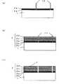
図1は、本発明の発光素子の製造方法の示す断面図である。 FIG. 1 is a cross-sectional view illustrating a method for manufacturing a light emitting device of the present invention.
図1において、1は成長用基板、2は光半導体層、2aはバッファ層、2bは第1導電型(n型)の半導体層、2cは発光層、2dは第2導電型(p型)の半導体層、2eはテンプレート層、3は第1の接合部、4は支持基板、5は金属体(第1の電極)、6は第2の接合部、7は導電層(第2の電極)、8は発光素子、10は成長抑制マスクパターンをそれぞれ示す。 In FIG. 1, 1 is a growth substrate, 2 is an optical semiconductor layer, 2a is a buffer layer, 2b is a first conductivity type (n-type) semiconductor layer, 2c is a light emitting layer, and 2d is a second conductivity type (p-type). Semiconductor layer, 2e is a template layer, 3 is a first joint, 4 is a support substrate, 5 is a metal body (first electrode), 6 is a second joint, and 7 is a conductive layer (second electrode). ), 8 denotes a light emitting element, and 10 denotes a growth suppression mask pattern.
本発明の発光素子の製造方法は、(1)成長用基板上に、光半導体層と第1の接合部とを順次積層して第1の積層体を複数形成する工程と、(2)支持基板の、前記成長用基板と対向させたとき前記第1の接合部と対向する位置に、金属体と第2の接合部とを順次積層して第2の積層体を複数形成する工程と、(3)加熱することにより前記第1の接合部と前記第2の接合部とを接合させて前記第1の積層体に前記第2の積層体を実装する工程と、(4)前記成長用基板を除去する工程と、(5)前記支持基板を除去して前記金属体を露出させ、第1の電極とする工程と、(6)前記光半導体素子上に導電層を形成して第2の電極とする工程と、を具備する。 The light emitting device manufacturing method of the present invention includes (1) a step of sequentially stacking an optical semiconductor layer and a first bonding portion on a growth substrate to form a plurality of first stacked bodies, and (2) support. Forming a plurality of second laminated bodies by sequentially laminating a metal body and a second joint at a position of the substrate facing the first joint when facing the growth substrate; (3) a step of bonding the first bonding portion and the second bonding portion by heating to mount the second stacked body on the first stacked body; and (4) the growth purpose. A step of removing the substrate; (5) a step of removing the support substrate to expose the metal body to form a first electrode; and (6) forming a conductive layer on the optical semiconductor element to form a second layer. And a step of forming an electrode.
以下にそれぞれの工程について説明する。 Each process will be described below.
(工程1)
工程1では、図1(a)に示すように、成長用基板1上に、光半導体層2と第1の接合部3とを順次積層して第1の積層体を複数形成する。(Process 1)
In
成長用基板1は、光半導体層2を成長させることが可能な基板であればよい。具体的に、基板1としては、サファイア(Al2O3)、窒化ガリウム(GaN)、窒化アルミニウム(AlN)、酸化亜鉛(ZnO),シリコンカーバイド(SiC)等が挙げられる。基板20aの厚みとしては、100μm〜1000μm程度である。The
光半導体層2としては、III族窒化物半導体、III−V族化合物半導体、II−VI族化合物半導体などが挙げられる。ここで、III族窒化物半導体とは、元素周期律表におけるIII族(13族)元素の窒化物から構成される半導体を意味する。III族窒化物半導体は化学式AlxGayIn1-x-yN(0≦x≦1、0≦y≦1、x+y≦1)で表すことができる。III族窒化物半導体としては、例えば、窒化ガリウム(GaN)、窒化アルミニウム(AlN)、窒化アルミニウムガリウム(AlGaN)、窒化インジウム(InN)などが挙げられる。Examples of the
図1(a)の場合、光半導体層2は、バッファ層2a、第1導電型の半導体層2b、発光層及2cおよび第2導電型の半導体層2dで構成される。 In the case of FIG. 1A, the
バッファ層2aは、成長用基板1と光半導体層2との間の応力を緩和させるために好適に形成される。バッファ層2aは、例えば、窒化ガリウム、窒化アルミニウムなどの材料から構成される。バッファ層2aの厚みは0.01〜0.2μm程度である。 The buffer layer 2 a is preferably formed in order to relieve stress between the
第1導電型の半導体層2bとしては、n型の半導体層が挙げられる。例えば、III族窒化物半導体層をn型とするには、元素周期律表においてIV族の元素であるSi等をドーパントとして窒化物半導体層に混入させればよい。第1導電型の半導体層2bの厚みは2〜3μm程度である。 Examples of the first conductivity
第2導電型の半導体層2dとしては、p型の窒化物半導体が挙げられる。例えば、III族窒化物半導体層をp型とするには、元素周期律表においてII族の元素であるMg等をドーパントとして窒化物半導体層に混入させればよい。第2導電型の半導体層2dの厚みは200〜500nm程度である。 Examples of the second conductivity type semiconductor layer 2d include a p-type nitride semiconductor. For example, in order to make the group III nitride semiconductor layer p-type, Mg or the like, which is a group II element in the periodic table, may be mixed into the nitride semiconductor layer as a dopant. The thickness of the second conductivity type semiconductor layer 2d is about 200 to 500 nm.
発光層2cは、第1導電型の半導体層2bと第2導電型の半導体層2dとの間に設けられる。発光層2cは、禁制帯幅の広い障壁層と禁制帯幅の狭い井戸層とから成る量子井戸構造が複数回(例えば約3回)繰り返し規則的に積層された多層量子井戸構造(MQW)としてもよい。なお、前記障壁層としては、In0.01Ga0.99N層などが挙げられる。また、井戸層としては、In0.11Ga0.89N層などが挙げられる。障壁層の厚みは5〜15nm程度、井戸層の厚みは2〜10nm程度である。発光層2cの厚みは25〜150nm程度である。The light emitting layer 2c is provided between the first conductive
成長用基板1上における光半導体層2の成長方法としては、分子線エピタキシー(MBE;Molecular Beam Epitaxy)法、有機金属エピタキシー(MOVPE;Metal Organic Vapor Phase Epitaxy)法、ハイドライド気相成長(HVPE;Hydride Vapor Phase Epitaxy)、パルスレーザデポジション(PLD;Pulsed Laser deposition)法等が用いられる。 As a growth method of the
工程1において、光半導体層2上に第1の接合部3を形成する。第1の接合部3は真空蒸着法、スパッタリング法等の方法により設けられ、厚みは0.1〜10μm程度である。また、第1の接合部3は、Au−Snの合金、Pb−Sn合金などの材料により構成される。 In
工程1において、第1の積層体を複数形成する方法としては、作製した第1の積層体を分割する方法、マスクを形成し成長用基板1の領域を先に分割させ、その後に第1の積層体を成長させる方法などが挙げられる。作製した第1の積層体を分割する方法としては、例えば、ダイシング、分割する領域以外にエッチングマスクを形成した後にドライエッチングを行う方法などが挙げられる。 In
また、成長用基板1の領域を先に分割させ、その後に第1の積層体を成長させる方法の具体例は、以下の図2に示す。 Further, a specific example of a method of dividing the region of the
まず、成長用基板1上に成長抑制マスクパターンを形成する(図2(a))。その際、バッファ層2a上にテンプレート層2eを成長させたのち、マスクを形成する領域だけエッチング等によりバッファ層2aおよびテンプレート層2eを除去しておく。なぜなら成長用基板はテンプレート層と分離されるので、テンプレート層を分割しておかないとテンプレート層では各々の半導体層は繋がったままになってしまうからである。ここで、テンプレート層2eとは、成長抑制マスク10上には成長させないように、半導体層2bを選択的に成長させるために用いられる。テンプレート層2eは、第1導電型の半導体層2bがバッファ層無しでエピタキシャル成長する材料であり、厚みは1〜5μm程度である。 First, a growth suppression mask pattern is formed on the growth substrate 1 (FIG. 2A). At this time, after the template layer 2e is grown on the buffer layer 2a, the buffer layer 2a and the template layer 2e are removed by etching or the like only in the region where the mask is to be formed. This is because the growth substrate is separated from the template layer, and each semiconductor layer remains connected to the template layer unless the template layer is divided. Here, the template layer 2e is used for selectively growing the
成長抑制マスクパターン10は、III族窒化物半導体のエピタキシャル成長に対して不活性の材料から成る物質により形成される。ここで、成長抑制マスクパターン10に使用される材料としては、具体的にはSiO2,多結晶シリコンなどが挙げられる。これらはIII族窒化物半導体のエピタキシャル成長に対して不活性である。The growth
成長抑制マスクパターン10は、具体的に、蒸着、CVD等によりマスク材料を一面に成膜した後、フォトリソグラフィおよびエッチングをすることにより形成される。 Specifically, the growth suppressing
成長抑制マスクパターン10を形成した後に、テンプレート層2e上に成長抑制マスクパターン10によって分離された、第1導電型の半導体層2bと、発光層2cと、第2導電型の半導体層2dと、を、エピタキシャル成長によって形成する(図2(b)参照)。 After forming the growth
そして、それらを形成したのちに、成長抑制マスクパターン10を除去させる(図2(c))。具体的に、マスク材料がSiO2の場合はフッ酸、多結晶シリコンの場合は硝酸及びフッ酸による混酸によるウェットエッチングをすることにより成長抑制マスクパターン10を除去する。Then, after forming them, the growth
(工程2)
工程2では、図1(b)に示すように、支持基板4の、成長用基板1と対向させたとき第1の接合部3と対向する位置に、金属体5と第2の接合部6とを順次積層して第2の積層体を複数形成する。(Process 2)
In
支持基板4は、アルミナ、窒化アルミ等のセラミックや、ガラス、ステンレス等の金属、ガラスエポキシ基板などの材料により構成される。支持基板4の材料は成長用基板1の材料と熱膨張係数が近いことが好ましい。支持基板4の厚みは0.5〜5mm程度である。 The
金属体5は、支持基板4上に、成長用基板1と対向させたとき第1の接合部3と対向する位置に複数作製される。平面視したときの金属体5の面積は、光半導体層2を平面視したときの面積と等しい、またはそれ以上である。このように、本発明の製造方法において金属体5は、チップサイズ(0.2〜5mm角程度)で使用される。 A plurality of
金属体5の作製方法としては、例えば、支持基板上に、ウェハサイズの金属体を設けてそれらを接合したのち、ダイシングにより、チップサイズに分割する方法などが挙げられる。 Examples of a method for producing the
金属体5としては、Cu−W合金などが挙げられるが、本発明の製造方法では、Cu単体から構成される金属体5を使用することが可能となる。従来では、例えば、成長用基板1としてサファイア基板を用いた場合、金属体5としては熱膨張係数がサファイア基板と近いCu−W合金が用いられていた。しかし、Cu−W合金は、熱伝導性が不十分であったため、より熱伝導性に優れるCu単体から構成される金属体5の使用が望まれていた。 Examples of the
本発明では、チップサイズの金属体5を用いることで、金属体と光半導体層との接続面積が小さくなる。これにより、ウェハサイズの金属体の場合と比較して、金属体と成長用基板との間の熱膨張率係数の差により発生する歪みを減少させることができるため、金属体5として、Cu単体を用いることが可能となる。 In the present invention, the connection area between the metal body and the optical semiconductor layer is reduced by using the chip-
第2の接合部6は、第1の接合部3と接合するための部位である。第2の接合部6はメッキ法、スパッタリング法、真空蒸着法などの方法により設けられ、厚みは1〜100μm程度である。また、第2の接合部6はAn−Sn合金、Pb−Sn合金などの材料により構成される。 The
工程2において、支持基板4と金属体5との間には、第3の接合部が設けられることが好ましい。これにより、支持基板4上に金属体5が十分に保持される。支持基板4と金属体5とは、150〜400℃に加熱することで行われる。 In
第3の接合部の融点は、第1の接合部3および第2の接合部6の融点よりも低いことが好ましい。このような第3の接合部としては、例えば、インジウム、スズ、鉛およびこれらの合金、UV硬化熱剥離接着剤などが挙げられる。 The melting point of the third bonding part is preferably lower than the melting points of the
第3の接合部の融点は、第1の接合部3および第2の接合部6の融点よりも低いことにより、後述する工程3において第1の接合部3と第2の接合部6とを接合させた後、温度が減少して接合部同士が凝固しても、第3の接合部は液体である期間が長い。よって、金属体5と支持体4の間の熱膨張係数の相違があったとしても、第3の接合部が緩衝となり、熱膨張係数の影響を小さくすることができる。 Since the melting point of the third bonding portion is lower than the melting points of the
(工程3)
工程3は、加熱することにより第1の接合部3と第2の接合部6とを接合させて第1の積層体に第2の積層体を実装する工程をいう(図1(c)参照)。第1の接合部3と第2の接合部6とは、150〜400℃に加熱することで行われる。(Process 3)
(工程4)
工程4において、成長用基板1を除去する。除去方法としては、レーザーリフトオフ(成長用基板1と光半導体層2とが異種材料の場合)、基板の研磨などが挙げられる。なかでもレーザー照射により簡易に成長用基板1を除去できるため、レーザーリフトオフが除去方法として好ましい。また、工程3において、加熱された際に、そのサイクルの中でレーザーリフトオフを行うようにしてもよい。この場合、成長用基板1が先に除去された状態で支持基板4が冷却されるので、熱応力の蓄積を防止することができる。(Process 4)
In
(工程5)
工程5において支持基板を除去して金属体5を露出させ、第1の電極とする。除去方法としては、例えば、加熱により第3の接合部を融かし、光半導体層2を真空吸着する方法などの方法が挙げられる。また、第3の接合部に、熱により剥離する接着剤を用いた場合は、工程3の熱処理で接着力が減少しているため、光半導体層2に粘着シートを貼り付けるだけで、光半導体層2は支持基板4から容易に除去される。(Process 5)
In
とくに金属体5と支持基板4との間に第3の接合部を設けており、その第3の接合部の融点が、第1の接合部3および第2の接合部6の融点よりも低い場合、工程5において、第1の接合部3および第2の接合部6の融点よりも低く、第3の接合部の融点よりも高い温度に加熱することで、第1および第2の接合部への影響の小さい状態で支持基板のみを除去することができる。 In particular, a third joint is provided between the
(工程6)
工程6において、光半導体素子2上に導電層7を形成して第2の電極とする。(Step 6)
In
導電層7は電流を素子全面に拡散させる為の導電部7aと、外部と電気的接触を取るパッド電極7bから構成される。導電部7aとしては、ITO、ZnOなどの透明導電膜材料、Ti, Al,Rhなどの金属材料が用いられる。 The
導電層7aは、真空蒸着法、スパッタリング法などの方法により作製される。また、導電層7aの厚みは約0.1〜5μmである。導電層7aは必ずしも無くても良く、導電層7aによる光の吸収を抑えつつ電流拡散の効果を得る為に、例えば格子状にパターニングしてあっても良い。 The conductive layer 7a is produced by a method such as a vacuum evaporation method or a sputtering method. The thickness of the conductive layer 7a is about 0.1 to 5 μm. The conductive layer 7a is not necessarily required, and may be patterned, for example, in a lattice pattern in order to obtain the effect of current diffusion while suppressing light absorption by the conductive layer 7a.
次にワイヤーボンディングを行う為のパッド電極7bを形成する。パッド電極7bは第1導電型の半導体層2bまたは導電部7aと接合できるように、例えば、チタン、またはチタンを下地層として金層を積層したものを用いる。 Next, a pad electrode 7b for wire bonding is formed. The pad electrode 7b is made of, for example, titanium or a layer in which a gold layer is stacked with titanium as a base layer so that the pad electrode 7b can be bonded to the first conductive
パッド電極7bは、真空蒸着法、スパッタリング法などの方法により形成される。パッド電極7bの厚みは約0.5〜5μmである。 The pad electrode 7b is formed by a method such as a vacuum evaporation method or a sputtering method. The thickness of the pad electrode 7b is about 0.5 to 5 μm.
以上のように、工程1〜6を経ることにより、発光素子8を作製することができる。 As described above, the light-emitting
なお、本発明は上記の実施の形態に限定されるものではなく、本発明の要旨を逸脱しない範囲内で種々の変更を施すことは何等差し支えない。 Note that the present invention is not limited to the above-described embodiment, and various modifications can be made without departing from the scope of the present invention.
1:成長用基板
2:光半導体層
2a:バッファ層
2b:第1導電型(n型)の半導体層
2c:発光層
2d:第2導電型(p型)の半導体層
2e:テンプレート層
3:第1の接合部
4:支持基板
5:金属体(第1の電極)
6:第2の接合部
7:導電層(第2の電極)
7a:導電部
7b:パッド電極
8:発光素子
10:成長抑制マスクパターン1: growth substrate 2: optical semiconductor layer 2a:
6: Second joint 7: Conductive layer (second electrode)
7a: Conductive portion 7b: Pad electrode 8: Light emitting element 10: Growth suppression mask pattern
Claims (5)
Translated fromJapanese(2)支持基板の、前記成長用基板と対向させたとき前記第1の接合部と対向する位置に、金属体と第2の接合部とを順次積層して第2の積層体を複数形成する工程と、
(3)加熱することにより前記第1の接合部と前記第2の接合部とを接合させて前記第1の積層体に前記第2の積層体を実装する工程と、
(4)前記成長用基板を除去する工程と、
(5)前記支持基板を除去して前記金属体を露出させ、第1の電極とする工程と、
(6)前記光半導体素子上に導電層を形成して第2の電極とする工程と、
を具備する発光素子の製造方法。(1) forming a plurality of first stacked bodies by sequentially stacking an optical semiconductor layer and a first bonding portion on a growth substrate;
(2) A plurality of second laminated bodies are formed by sequentially laminating a metal body and a second joint portion at a position facing the first joint portion when the support substrate is opposed to the growth substrate. And a process of
(3) The step of bonding the first bonding portion and the second bonding portion by heating to mount the second stacked body on the first stacked body;
(4) removing the growth substrate;
(5) removing the support substrate to expose the metal body to form a first electrode;
(6) forming a conductive layer on the optical semiconductor element to form a second electrode;
A method for manufacturing a light emitting device comprising:
(1−1)前記成長用基板上に、前記第1の積層体のエピタキシャル成長に対して不活性な材料から成る物質により成長抑制マスクパターンを形成して、相互に分離された複数の前記成長用基板上に露出部を形成する工程と、
(1−2)前記成長用基板上の露出部に、エピタキシャル成長によって前記第1の積層体を複数形成する工程と、
(1−3)前記成長抑制マスクパターンを除去する工程と、
を含む請求項1記載の発光素子の製造方法。The step (1)
(1-1) A plurality of growth-use patterns separated from each other by forming a growth-inhibiting mask pattern on the growth-use substrate using a material made of a material that is inactive with respect to the epitaxial growth of the first stacked body. Forming an exposed portion on the substrate;
(1-2) forming a plurality of the first stacked bodies by epitaxial growth on the exposed portion on the growth substrate;
(1-3) removing the growth suppression mask pattern;
The manufacturing method of the light emitting element of Claim 1 containing this.
前記工程(5)において、前記第1の接合部および前記第2の接合部の融点よりも低く、前記第3の接合部の融点よりも高い温度に前記支持基板と前記金属体とを加熱することにより前記支持基板を除去する請求項1乃至4のいずれか記載の発光素子の製造方法。In the step (2), the support substrate and the metal body are bonded via a third bonding portion having a melting point lower than that of the first bonding portion and the second bonding portion. ,
In the step (5), the support substrate and the metal body are heated to a temperature lower than the melting points of the first bonding portion and the second bonding portion and higher than the melting point of the third bonding portion. The method for manufacturing a light-emitting element according to claim 1, wherein the support substrate is removed.
Priority Applications (1)
| Application Number | Priority Date | Filing Date | Title |
|---|---|---|---|
| JP2008222508AJP2010056458A (en) | 2008-08-29 | 2008-08-29 | Method of manufacturing light emitting element |
Applications Claiming Priority (1)
| Application Number | Priority Date | Filing Date | Title |
|---|---|---|---|
| JP2008222508AJP2010056458A (en) | 2008-08-29 | 2008-08-29 | Method of manufacturing light emitting element |
Publications (1)
| Publication Number | Publication Date |
|---|---|
| JP2010056458Atrue JP2010056458A (en) | 2010-03-11 |
Family
ID=42072027
Family Applications (1)
| Application Number | Title | Priority Date | Filing Date |
|---|---|---|---|
| JP2008222508APendingJP2010056458A (en) | 2008-08-29 | 2008-08-29 | Method of manufacturing light emitting element |
Country Status (1)
| Country | Link |
|---|---|
| JP (1) | JP2010056458A (en) |
Cited By (44)
| Publication number | Priority date | Publication date | Assignee | Title |
|---|---|---|---|---|
| JP2012089646A (en)* | 2010-10-19 | 2012-05-10 | Napura:Kk | Light-emitting device and method of manufacturing the same |
| JP2012238795A (en)* | 2011-05-13 | 2012-12-06 | Stanley Electric Co Ltd | Semiconductor element manufacturing method |
| WO2013074374A1 (en)* | 2011-11-18 | 2013-05-23 | LuxVue Technology Corporation | Micro light emitting diode |
| US8518204B2 (en) | 2011-11-18 | 2013-08-27 | LuxVue Technology Corporation | Method of fabricating and transferring a micro device and an array of micro devices utilizing an intermediate electrically conductive bonding layer |
| EP2631948A2 (en) | 2012-02-21 | 2013-08-28 | Stanley Electric Co., Ltd. | Semiconductor light emitting element, method of manufacturing the same, and vehicle lighting unit utilizing the same |
| US8573469B2 (en) | 2011-11-18 | 2013-11-05 | LuxVue Technology Corporation | Method of forming a micro LED structure and array of micro LED structures with an electrically insulating layer |
| US8646505B2 (en) | 2011-11-18 | 2014-02-11 | LuxVue Technology Corporation | Micro device transfer head |
| US8686542B2 (en) | 2012-07-06 | 2014-04-01 | LuxVue Technology Corporation | Compliant monopolar micro device transfer head with silicon electrode |
| KR20140053530A (en)* | 2012-10-26 | 2014-05-08 | 삼성전자주식회사 | Semiconductor light emitting device and manufacturing method of the same |
| US8789573B2 (en) | 2011-11-18 | 2014-07-29 | LuxVue Technology Corporation | Micro device transfer head heater assembly and method of transferring a micro device |
| US8791530B2 (en) | 2012-09-06 | 2014-07-29 | LuxVue Technology Corporation | Compliant micro device transfer head with integrated electrode leads |
| US8928021B1 (en) | 2013-06-18 | 2015-01-06 | LuxVue Technology Corporation | LED light pipe |
| US8987765B2 (en) | 2013-06-17 | 2015-03-24 | LuxVue Technology Corporation | Reflective bank structure and method for integrating a light emitting device |
| US9012930B2 (en) | 2012-09-13 | 2015-04-21 | Stanley Electric Co., Ltd. | Semiconductor light emitting device providing graded brightness |
| US9035279B2 (en) | 2013-07-08 | 2015-05-19 | LuxVue Technology Corporation | Micro device with stabilization post |
| US9087764B2 (en) | 2013-07-26 | 2015-07-21 | LuxVue Technology Corporation | Adhesive wafer bonding with controlled thickness variation |
| US9105492B2 (en) | 2012-05-08 | 2015-08-11 | LuxVue Technology Corporation | Compliant micro device transfer head |
| US9111464B2 (en) | 2013-06-18 | 2015-08-18 | LuxVue Technology Corporation | LED display with wavelength conversion layer |
| US9136161B2 (en) | 2013-06-04 | 2015-09-15 | LuxVue Technology Corporation | Micro pick up array with compliant contact |
| US9153548B2 (en) | 2013-09-16 | 2015-10-06 | Lux Vue Technology Corporation | Adhesive wafer bonding with sacrificial spacers for controlled thickness variation |
| US9217541B2 (en) | 2013-05-14 | 2015-12-22 | LuxVue Technology Corporation | Stabilization structure including shear release posts |
| US9236815B2 (en) | 2012-12-10 | 2016-01-12 | LuxVue Technology Corporation | Compliant micro device transfer head array with metal electrodes |
| US9296111B2 (en) | 2013-07-22 | 2016-03-29 | LuxVue Technology Corporation | Micro pick up array alignment encoder |
| US9318475B2 (en) | 2014-05-15 | 2016-04-19 | LuxVue Technology Corporation | Flexible display and method of formation with sacrificial release layer |
| US9367094B2 (en) | 2013-12-17 | 2016-06-14 | Apple Inc. | Display module and system applications |
| US9425151B2 (en) | 2014-06-17 | 2016-08-23 | Apple Inc. | Compliant electrostatic transfer head with spring support layer |
| US9450147B2 (en) | 2013-12-27 | 2016-09-20 | Apple Inc. | LED with internally confined current injection area |
| US9478583B2 (en) | 2014-12-08 | 2016-10-25 | Apple Inc. | Wearable display having an array of LEDs on a conformable silicon substrate |
| US9484504B2 (en) | 2013-05-14 | 2016-11-01 | Apple Inc. | Micro LED with wavelength conversion layer |
| US9511498B2 (en) | 2012-09-07 | 2016-12-06 | Apple Inc. | Mass transfer tool |
| US9522468B2 (en) | 2014-05-08 | 2016-12-20 | Apple Inc. | Mass transfer tool manipulator assembly with remote center of compliance |
| US9542638B2 (en) | 2014-02-18 | 2017-01-10 | Apple Inc. | RFID tag and micro chip integration design |
| US9548332B2 (en) | 2012-04-27 | 2017-01-17 | Apple Inc. | Method of forming a micro LED device with self-aligned metallization stack |
| US9558721B2 (en) | 2012-10-15 | 2017-01-31 | Apple Inc. | Content-based adaptive refresh schemes for low-power displays |
| US9570002B2 (en) | 2014-06-17 | 2017-02-14 | Apple Inc. | Interactive display panel with IR diodes |
| US9583466B2 (en) | 2013-12-27 | 2017-02-28 | Apple Inc. | Etch removal of current distribution layer for LED current confinement |
| US9583533B2 (en) | 2014-03-13 | 2017-02-28 | Apple Inc. | LED device with embedded nanowire LEDs |
| US9624100B2 (en) | 2014-06-12 | 2017-04-18 | Apple Inc. | Micro pick up array pivot mount with integrated strain sensing elements |
| US9705432B2 (en) | 2014-09-30 | 2017-07-11 | Apple Inc. | Micro pick up array pivot mount design for strain amplification |
| US9741286B2 (en) | 2014-06-03 | 2017-08-22 | Apple Inc. | Interactive display panel with emitting and sensing diodes |
| US9768345B2 (en) | 2013-12-20 | 2017-09-19 | Apple Inc. | LED with current injection confinement trench |
| US9773750B2 (en) | 2012-02-09 | 2017-09-26 | Apple Inc. | Method of transferring and bonding an array of micro devices |
| US9828244B2 (en) | 2014-09-30 | 2017-11-28 | Apple Inc. | Compliant electrostatic transfer head with defined cavity |
| JP2022523861A (en)* | 2019-03-12 | 2022-04-26 | ザ リージェンツ オブ ザ ユニバーシティ オブ カリフォルニア | A method for removing the bar of one or more elements using a support plate |
- 2008
- 2008-08-29JPJP2008222508Apatent/JP2010056458A/enactivePending
Cited By (96)
| Publication number | Priority date | Publication date | Assignee | Title |
|---|---|---|---|---|
| US8766312B2 (en) | 2010-10-19 | 2014-07-01 | Napra Co., Ltd. | Light-emitting device comprising vertical conductors and through electrodes and method for manufacturing the same |
| CN102456827A (en)* | 2010-10-19 | 2012-05-16 | 纳普拉有限公司 | Light-emitting device and method for manufacturing the same |
| JP2012089646A (en)* | 2010-10-19 | 2012-05-10 | Napura:Kk | Light-emitting device and method of manufacturing the same |
| JP2012238795A (en)* | 2011-05-13 | 2012-12-06 | Stanley Electric Co Ltd | Semiconductor element manufacturing method |
| US8809875B2 (en) | 2011-11-18 | 2014-08-19 | LuxVue Technology Corporation | Micro light emitting diode |
| US12243955B2 (en) | 2011-11-18 | 2025-03-04 | Apple Inc. | Display and micro device array for transfer to a display substrate |
| US9463613B2 (en) | 2011-11-18 | 2016-10-11 | Apple Inc. | Micro device transfer head heater assembly and method of transferring a micro device |
| US8552436B2 (en) | 2011-11-18 | 2013-10-08 | LuxVue Technology Corporation | Light emitting diode structure |
| US8558243B2 (en) | 2011-11-18 | 2013-10-15 | LuxVue Technology Corporation | Micro device array for transfer to a receiving substrate |
| US8573469B2 (en) | 2011-11-18 | 2013-11-05 | LuxVue Technology Corporation | Method of forming a micro LED structure and array of micro LED structures with an electrically insulating layer |
| US9620478B2 (en) | 2011-11-18 | 2017-04-11 | Apple Inc. | Method of fabricating a micro device transfer head |
| US8646505B2 (en) | 2011-11-18 | 2014-02-11 | LuxVue Technology Corporation | Micro device transfer head |
| US10607961B2 (en) | 2011-11-18 | 2020-03-31 | Apple Inc. | Micro device transfer head heater assembly and method of transferring a micro device |
| WO2013074374A1 (en)* | 2011-11-18 | 2013-05-23 | LuxVue Technology Corporation | Micro light emitting diode |
| WO2013074375A1 (en)* | 2011-11-18 | 2013-05-23 | LuxVue Technology Corporation | Method of forming a micro light emitting diode array |
| US8789573B2 (en) | 2011-11-18 | 2014-07-29 | LuxVue Technology Corporation | Micro device transfer head heater assembly and method of transferring a micro device |
| US9831383B2 (en) | 2011-11-18 | 2017-11-28 | Apple Inc. | LED array |
| US8794501B2 (en) | 2011-11-18 | 2014-08-05 | LuxVue Technology Corporation | Method of transferring a light emitting diode |
| US10121864B2 (en) | 2011-11-18 | 2018-11-06 | Apple Inc. | Micro device transfer head heater assembly and method of transferring a micro device |
| US11552046B2 (en) | 2011-11-18 | 2023-01-10 | Apple Inc. | Micro device transfer head assembly |
| US10297712B2 (en) | 2011-11-18 | 2019-05-21 | Apple Inc. | Micro LED display |
| US8518204B2 (en) | 2011-11-18 | 2013-08-27 | LuxVue Technology Corporation | Method of fabricating and transferring a micro device and an array of micro devices utilizing an intermediate electrically conductive bonding layer |
| US9773750B2 (en) | 2012-02-09 | 2017-09-26 | Apple Inc. | Method of transferring and bonding an array of micro devices |
| US8952415B2 (en) | 2012-02-21 | 2015-02-10 | Stanley Electric Co., Ltd. | Semiconductor light emitting element, method of manufacturing the same, and vehicle lighting unit utilizing the same |
| EP2631948A3 (en)* | 2012-02-21 | 2014-01-22 | Stanley Electric Co., Ltd. | Semiconductor light emitting element, method of manufacturing the same, and vehicle lighting unit utilizing the same |
| EP2631948A2 (en) | 2012-02-21 | 2013-08-28 | Stanley Electric Co., Ltd. | Semiconductor light emitting element, method of manufacturing the same, and vehicle lighting unit utilizing the same |
| US9548332B2 (en) | 2012-04-27 | 2017-01-17 | Apple Inc. | Method of forming a micro LED device with self-aligned metallization stack |
| US9105492B2 (en) | 2012-05-08 | 2015-08-11 | LuxVue Technology Corporation | Compliant micro device transfer head |
| US9370864B2 (en) | 2012-05-08 | 2016-06-21 | Apple Inc. | Compliant micro device transfer head |
| US9895902B2 (en) | 2012-05-08 | 2018-02-20 | Apple Inc. | Compliant micro device transfer head |
| US9505230B2 (en) | 2012-05-08 | 2016-11-29 | Apple Inc. | Compliant micro device transfer head |
| US8686542B2 (en) | 2012-07-06 | 2014-04-01 | LuxVue Technology Corporation | Compliant monopolar micro device transfer head with silicon electrode |
| US9000566B2 (en) | 2012-07-06 | 2015-04-07 | LuxVue Technology Corporation | Compliant micro device transfer head |
| US8791530B2 (en) | 2012-09-06 | 2014-07-29 | LuxVue Technology Corporation | Compliant micro device transfer head with integrated electrode leads |
| US8945968B2 (en) | 2012-09-06 | 2015-02-03 | LuxVue Technology Corporation | Compliant micro device transfer head with integrated electrode leads |
| US10183401B2 (en) | 2012-09-07 | 2019-01-22 | Apple Inc. | Mass transfer tool |
| US9511498B2 (en) | 2012-09-07 | 2016-12-06 | Apple Inc. | Mass transfer tool |
| US9012930B2 (en) | 2012-09-13 | 2015-04-21 | Stanley Electric Co., Ltd. | Semiconductor light emitting device providing graded brightness |
| US9240522B2 (en) | 2012-09-13 | 2016-01-19 | Stanley Electric Co., Ltd. | Semiconductor light emitting device providing graded brightness |
| US9558721B2 (en) | 2012-10-15 | 2017-01-31 | Apple Inc. | Content-based adaptive refresh schemes for low-power displays |
| KR20140053530A (en)* | 2012-10-26 | 2014-05-08 | 삼성전자주식회사 | Semiconductor light emitting device and manufacturing method of the same |
| KR101969308B1 (en)* | 2012-10-26 | 2019-04-17 | 삼성전자주식회사 | Semiconductor light emitting device and manufacturing method of the same |
| US9236815B2 (en) | 2012-12-10 | 2016-01-12 | LuxVue Technology Corporation | Compliant micro device transfer head array with metal electrodes |
| US9217541B2 (en) | 2013-05-14 | 2015-12-22 | LuxVue Technology Corporation | Stabilization structure including shear release posts |
| US9484504B2 (en) | 2013-05-14 | 2016-11-01 | Apple Inc. | Micro LED with wavelength conversion layer |
| US9136161B2 (en) | 2013-06-04 | 2015-09-15 | LuxVue Technology Corporation | Micro pick up array with compliant contact |
| US9484237B2 (en) | 2013-06-04 | 2016-11-01 | Apple Inc. | Mass transfer system |
| US11004836B2 (en) | 2013-06-17 | 2021-05-11 | Apple Inc. | Method for integrating a light emitting device |
| US9240397B2 (en) | 2013-06-17 | 2016-01-19 | LuxVue Technology Corporation | Method for integrating a light emitting device |
| US10573629B2 (en) | 2013-06-17 | 2020-02-25 | Apple Inc. | Method for integrating a light emitting device |
| US8987765B2 (en) | 2013-06-17 | 2015-03-24 | LuxVue Technology Corporation | Reflective bank structure and method for integrating a light emitting device |
| US10256221B2 (en) | 2013-06-17 | 2019-04-09 | Apple Inc. | Method for integrating a light emitting device |
| US9570427B2 (en) | 2013-06-17 | 2017-02-14 | Apple Inc. | Method for integrating a light emitting device |
| US11676952B2 (en) | 2013-06-17 | 2023-06-13 | Apple Inc. | Method for integrating a light emitting device |
| US9876000B2 (en) | 2013-06-17 | 2018-01-23 | Apple Inc. | Method for integrating a light emitting device |
| US12094864B2 (en) | 2013-06-17 | 2024-09-17 | Apple Inc. | Light emitting structure |
| US9865577B2 (en) | 2013-06-18 | 2018-01-09 | Apple Inc. | LED display with wavelength conversion layer |
| US8928021B1 (en) | 2013-06-18 | 2015-01-06 | LuxVue Technology Corporation | LED light pipe |
| US9111464B2 (en) | 2013-06-18 | 2015-08-18 | LuxVue Technology Corporation | LED display with wavelength conversion layer |
| US9599857B2 (en) | 2013-06-18 | 2017-03-21 | Apple Inc. | LED display with wavelength conversion layer |
| US9035279B2 (en) | 2013-07-08 | 2015-05-19 | LuxVue Technology Corporation | Micro device with stabilization post |
| US9620695B2 (en) | 2013-07-08 | 2017-04-11 | Apple Inc. | Micro device with stabilization post |
| US9379092B2 (en) | 2013-07-08 | 2016-06-28 | Apple Inc. | Micro device with stabilization post |
| US9209348B2 (en) | 2013-07-08 | 2015-12-08 | LuxVue Technology Corporation | Micro device with stabilization post |
| US9296111B2 (en) | 2013-07-22 | 2016-03-29 | LuxVue Technology Corporation | Micro pick up array alignment encoder |
| US9087764B2 (en) | 2013-07-26 | 2015-07-21 | LuxVue Technology Corporation | Adhesive wafer bonding with controlled thickness variation |
| US9153548B2 (en) | 2013-09-16 | 2015-10-06 | Lux Vue Technology Corporation | Adhesive wafer bonding with sacrificial spacers for controlled thickness variation |
| US9922966B2 (en) | 2013-12-17 | 2018-03-20 | Apple Inc. | Display module and system applications |
| US9367094B2 (en) | 2013-12-17 | 2016-06-14 | Apple Inc. | Display module and system applications |
| US11676953B2 (en) | 2013-12-17 | 2023-06-13 | Apple Inc. | Display module and system applications |
| US12087749B2 (en) | 2013-12-17 | 2024-09-10 | Apple Inc. | Display module and system applications |
| US10957678B2 (en) | 2013-12-17 | 2021-03-23 | Apple Inc. | Display module and system applications |
| US9582036B2 (en) | 2013-12-17 | 2017-02-28 | Apple Inc. | Display module and system applications |
| US10147711B2 (en) | 2013-12-17 | 2018-12-04 | Apple Inc. | Display module and system applications |
| US10535642B2 (en) | 2013-12-17 | 2020-01-14 | Apple Inc. | Display module and system applications |
| US11362076B2 (en) | 2013-12-17 | 2022-06-14 | Apple Inc | Display module and system applications |
| US9768345B2 (en) | 2013-12-20 | 2017-09-19 | Apple Inc. | LED with current injection confinement trench |
| US9450147B2 (en) | 2013-12-27 | 2016-09-20 | Apple Inc. | LED with internally confined current injection area |
| US11101405B2 (en) | 2013-12-27 | 2021-08-24 | Apple Inc. | LED with internally confined current injection area |
| US11978825B2 (en) | 2013-12-27 | 2024-05-07 | Apple Inc. | LED with internally confined current injection area |
| US9583466B2 (en) | 2013-12-27 | 2017-02-28 | Apple Inc. | Etch removal of current distribution layer for LED current confinement |
| US10593832B2 (en) | 2013-12-27 | 2020-03-17 | Apple Inc. | LED with internally confined current injection area |
| US9542638B2 (en) | 2014-02-18 | 2017-01-10 | Apple Inc. | RFID tag and micro chip integration design |
| US9583533B2 (en) | 2014-03-13 | 2017-02-28 | Apple Inc. | LED device with embedded nanowire LEDs |
| US9522468B2 (en) | 2014-05-08 | 2016-12-20 | Apple Inc. | Mass transfer tool manipulator assembly with remote center of compliance |
| US10183396B2 (en) | 2014-05-08 | 2019-01-22 | Apple Inc. | Mass transfer tool manipulator assembly with remote center of compliance |
| US9318475B2 (en) | 2014-05-15 | 2016-04-19 | LuxVue Technology Corporation | Flexible display and method of formation with sacrificial release layer |
| US9741286B2 (en) | 2014-06-03 | 2017-08-22 | Apple Inc. | Interactive display panel with emitting and sensing diodes |
| US10150669B2 (en) | 2014-06-12 | 2018-12-11 | Apple Inc. | Micro pick up array pivot mount |
| US9624100B2 (en) | 2014-06-12 | 2017-04-18 | Apple Inc. | Micro pick up array pivot mount with integrated strain sensing elements |
| US9570002B2 (en) | 2014-06-17 | 2017-02-14 | Apple Inc. | Interactive display panel with IR diodes |
| US9425151B2 (en) | 2014-06-17 | 2016-08-23 | Apple Inc. | Compliant electrostatic transfer head with spring support layer |
| US9828244B2 (en) | 2014-09-30 | 2017-11-28 | Apple Inc. | Compliant electrostatic transfer head with defined cavity |
| US9705432B2 (en) | 2014-09-30 | 2017-07-11 | Apple Inc. | Micro pick up array pivot mount design for strain amplification |
| US9478583B2 (en) | 2014-12-08 | 2016-10-25 | Apple Inc. | Wearable display having an array of LEDs on a conformable silicon substrate |
| JP2022523861A (en)* | 2019-03-12 | 2022-04-26 | ザ リージェンツ オブ ザ ユニバーシティ オブ カリフォルニア | A method for removing the bar of one or more elements using a support plate |
Similar Documents
| Publication | Publication Date | Title |
|---|---|---|
| JP2010056458A (en) | Method of manufacturing light emitting element | |
| KR101438818B1 (en) | light emitting diode | |
| KR101198758B1 (en) | Vertical structured semiconductor light emitting device and method for producing thereof | |
| JP5220916B2 (en) | Light emitting device and manufacturing method thereof | |
| CN102106006B (en) | Support substrate for manufacturing semiconductor light emitting device and semiconductor light emitting device using support substrate | |
| KR101470020B1 (en) | epitaxial semiconductor thin-film transfer using sandwich-structured wafer bonding and photon-beam | |
| US8946745B2 (en) | Supporting substrate for manufacturing vertically-structured semiconductor light-emitting device and semiconductor light-emitting device using the supporting substrate | |
| US7943942B2 (en) | Semiconductor light-emitting device with double-sided passivation | |
| CN102255013B (en) | Method for making light-emitting diode with vertical structure through stripping GaN based epitaxial layer and sapphire substrate by using wet process | |
| KR20130029455A (en) | Manufacturing method for gan semiconductor device | |
| CN112186079A (en) | Preparation method of LED chip with vertical structure | |
| US20150325742A1 (en) | Method of fabricating semiconductor devices | |
| KR100999548B1 (en) | A support substrate for manufacturing a semiconductor light emitting device having a vertical structure, a method for manufacturing a semiconductor light emitting device having a vertical structure and a semiconductor light emitting device having a vertical structure | |
| CN111771256A (en) | Manufacturing method of semiconductor element and semiconductor element | |
| KR101428066B1 (en) | vertical structured group 3 nitride-based light emitting diode and its fabrication methods | |
| JP5564799B2 (en) | Method for fabricating gallium nitride based semiconductor electronic device | |
| KR20100109169A (en) | Fabrication method of light emitting diode and the light emitting diode fabricated by the method | |
| KR101480551B1 (en) | vertical structured group 3 nitride-based light emitting diode and its fabrication methods | |
| KR101137514B1 (en) | Method for manufacturing nitride semiconductor device using nano particle | |
| JP2010226023A (en) | Method for manufacturing substrate product having nitride-based compound semiconductor layer on support substrate, and method for manufacturing semiconductor device | |
| KR101231118B1 (en) | Supporting substrates for semiconductor light emitting device and high-performance vertical structured semiconductor light emitting devices using supporting substrates | |
| KR20090115902A (en) | Vertical group III-nitride semiconductor light emitting diode device and manufacturing method | |
| JP2010056457A (en) | Method of manufacturing light emitting element array | |
| JP5800568B2 (en) | Manufacturing method of semiconductor device | |
| US8552465B2 (en) | Method for reducing stress in epitaxial growth |