Movatterモバイル変換


[0]ホーム

URL:


JP2010052288A - Fine structure transfer mold and fine structure transfer device - Google Patents

Fine structure transfer mold and fine structure transfer device
Download PDF

Info

Publication number
JP2010052288A
JP2010052288AJP2008219972AJP2008219972AJP2010052288AJP 2010052288 AJP2010052288 AJP 2010052288AJP 2008219972 AJP2008219972 AJP 2008219972AJP 2008219972 AJP2008219972 AJP 2008219972AJP 2010052288 AJP2010052288 AJP 2010052288A
Authority
JP
Japan
Prior art keywords
transfer mold
microstructure
microstructure transfer
transfer
fine structure
Prior art date
Legal status (The legal status is an assumption and is not a legal conclusion. Google has not performed a legal analysis and makes no representation as to the accuracy of the status listed.)
Granted
Application number
JP2008219972A
Other languages
Japanese (ja)
Other versions
JP5161707B2 (en
Inventor
Masahiko Ogino
雅彦 荻野
Mitsuru Hasegawa
長谷川  満
Akihiro Miyauchi
昭浩 宮内
Kazunari Sukai
一成 須貝
Daisuke Shimao
大輔 島尾
Current Assignee (The listed assignees may be inaccurate. Google has not performed a legal analysis and makes no representation or warranty as to the accuracy of the list.)
Hitachi Industrial Equipment Systems Co Ltd
Original Assignee
Hitachi Industrial Equipment Systems Co Ltd
Priority date (The priority date is an assumption and is not a legal conclusion. Google has not performed a legal analysis and makes no representation as to the accuracy of the date listed.)
Filing date
Publication date
Application filed by Hitachi Industrial Equipment Systems Co LtdfiledCriticalHitachi Industrial Equipment Systems Co Ltd
Priority to JP2008219972ApriorityCriticalpatent/JP5161707B2/en
Publication of JP2010052288ApublicationCriticalpatent/JP2010052288A/en
Application grantedgrantedCritical
Publication of JP5161707B2publicationCriticalpatent/JP5161707B2/en
Expired - Fee Relatedlegal-statusCriticalCurrent
Anticipated expirationlegal-statusCritical

Links

Images

Landscapes

Abstract

Translated fromJapanese

【課題】本発明の課題は、使用可能な被転写体のサイズが制限されないように微細構造転写装置に十分な保持力で保持させることができ、耐久性に優れた微細構造転写モールドを提供することにある。
【解決手段】本発明の微細構造転写モールド1aは、表面に微細な凹凸が形成されたパターン部2aと、このパターン部2aの外側に形成された固定部3aと、前記パターン部2aが前記固定部3aよりも突出するように前記パターン部2aと前記固定部3aとの間に設けられる傾斜部4aと、を備えることを特徴とする。
【選択図】図2
An object of the present invention is to provide a microstructure transfer mold that can be held in a microstructure transfer apparatus with sufficient holding force so that the size of a transferable material that can be used is not limited, and has excellent durability. There is.
A microstructure transfer mold 1a according to the present invention includes a pattern portion 2a having fine irregularities formed on a surface thereof, a fixing portion 3a formed outside the pattern portion 2a, and the pattern portion 2a being fixed. It is provided with the inclination part 4a provided between the said pattern part 2a and the said fixing | fixed part 3a so that it may protrude rather than the part 3a.
[Selection] Figure 2

Description

Translated fromJapanese

本発明は、被転写体の表面に、微細な凹凸からなる微細パターンを転写する微細構造転写モールド及び微細構造転写装置に関する。  The present invention relates to a fine structure transfer mold and a fine structure transfer apparatus for transferring a fine pattern composed of fine irregularities onto the surface of a transfer object.

近年、半導体集積回路は微細化及び集積化が進んでおり、その微細加工を実現するためのパターン転写技術としてフォトリソグラフィ装置の高精度化が進められてきた。しかし、加工方法が光露光の光源の波長に近づき、リソグラフィ技術も限界に近づいてきた。そのため、さらなる半導体集積回路の微細化及び集積化、並びに微細加工装置の高精度化を進めるために、リソグラフィ技術に代わり、荷電粒子線装置の一種である電子線描画装置が用いられるようになった。  2. Description of the Related Art In recent years, semiconductor integrated circuits have been miniaturized and integrated, and photolithography apparatuses have been improved in accuracy as a pattern transfer technique for realizing the fine processing. However, the processing method has approached the wavelength of the light source for light exposure, and the lithography technology has also approached its limit. Therefore, in order to advance further miniaturization and integration of semiconductor integrated circuits and higher precision of microfabrication apparatuses, an electron beam lithography apparatus, which is a kind of charged particle beam apparatus, has been used in place of lithography technology. .

電子ビームを用いたパターン形成法は、i線、エキシマレーザ等の光源を用いたパターン形成における一括露光方法とは異なり、マスクパターンを描画していく。そのため、描画するパターンが多いほど露光(描画)に時間を要し、パターン形成にも時間がかかることが欠点とされている。そして、256メガ、1ギガ、4ギガと、集積度が飛躍的に高まるにつれて、パターン形成の時間も飛躍的に長くなることになり、スループットが著しく劣ることが懸念される。そこで、電子ビーム描画装置の高速化のために、各種形状のマスクを組み合わせ、それらに一括して電子ビームを照射してマスクの組み合わせに対応した複雑な形状の電子ビームを形成する一括図形照射法の開発が進められている。この結果、パターンの微細化が進められる一方で、電子ビーム描画装置が大型化すると共にマスク位置をより高精度に制御する機構が必要になるので、装置コストが高くなるという欠点がある。  Unlike the batch exposure method in pattern formation using a light source such as i-line or excimer laser, the pattern formation method using an electron beam draws a mask pattern. Therefore, the more patterns to be drawn, the more time is required for exposure (drawing), and the longer time is required for pattern formation. As the degree of integration increases dramatically, such as 256 mega, 1 giga, and 4 giga, the pattern formation time also increases remarkably, and there is a concern that the throughput is significantly inferior. Therefore, in order to increase the speed of the electron beam lithography system, a combined figure irradiation method that combines various shaped masks and collectively irradiates them with electron beams to form complex shaped electron beams corresponding to the mask combinations. Development is underway. As a result, while miniaturization of the pattern is promoted, the electron beam lithography apparatus is increased in size and a mechanism for controlling the mask position with higher accuracy is required.

これに対し、微細なパターン形成を低コストで行うための技術が特許文献1及び特許文献2、並びに非特許文献1に開示されている。この技術は、形成する微細な凹凸パターンと同じ凹凸パターンを有するモールド(以下に、「微細構造転写モールド」ということがある)を、被転写体に対して型押しすることで凹凸パターンを転写するものである。特に特許文献2及び非特許文献1のナノインプリント技術では、シリコンウエハで形成した微細構造転写モールドを組み込んだ微細構造転写装置を使用して、25ナノメートル以下の微細な凹凸パターンが被転写体に転写されている。
米国特許5259926号明細書米国特許5772905号明細書S.Y.Chou et al.、Appl.Phys.Lett.、vol.67、 p.3314 (1995)
On the other hand, Patent Document 1, Patent Document 2, and Non-Patent Document 1 disclose techniques for forming a fine pattern at a low cost. In this technique, a concavo-convex pattern is transferred by embossing a mold having a concavo-convex pattern that is the same as the fine concavo-convex pattern to be formed (hereinafter sometimes referred to as a “microstructure transfer mold”) against the transfer target. Is. In particular, in the nanoimprint technology disclosed in Patent Document 2 and Non-Patent Document 1, a fine concavo-convex pattern of 25 nanometers or less is transferred to a transfer object using a fine structure transfer device incorporating a fine structure transfer mold formed of a silicon wafer. Has been.
US Pat. No. 5,259,926 US Pat. No. 5,772,905 SYChou et al., Appl.Phys.Lett., Vol.67, p.3314 (1995)

しかし、シリコンウエハで形成した微細構造転写モールドを微細構造転写装置に組み込むには、微細構造転写モールドの周辺部を治具等で機械的に保持するか、又は微細構造転写モールドの裏面に設けた基材を真空吸着又は接着によって保持する必要がある。そして、これらの保持方法のうち、微細構造転写モールドの周辺部を治具等で保持する方法では、微細構造転写モールドと被転写体とを接触する際に、治具等が被転写体に干渉するので、被転写体のサイズが微細構造転写モールドの治具等で囲まれたエリアの面積よりも小さい面積のものに制限される。また、微細構造転写モールドの裏面に設けた基材を真空吸着によって保持する方法では、微細構造転写モールドと被転写体との密着力が真空吸着力よりも大きいと、型押しした微細構造転写モールドを被転写体から剥離することができない。
そして、このような従来の微細構造転写モールドは、被転写体に対して型押しと剥離とが行われるたびに微細構造転写モールドの周縁部、つまりパターン形成部の外端に応力が集中するので、更なる耐久性の向上が望まれている。
However, in order to incorporate a microstructure transfer mold formed of a silicon wafer into a microstructure transfer apparatus, the periphery of the microstructure transfer mold is mechanically held by a jig or the like, or provided on the back surface of the microstructure transfer mold. It is necessary to hold the substrate by vacuum suction or adhesion. Of these holding methods, in the method of holding the periphery of the microstructure transfer mold with a jig or the like, the jig or the like interferes with the transferred object when the microstructure transfer mold and the transferred object are brought into contact with each other. Therefore, the size of the transfer object is limited to an area smaller than the area of the area surrounded by the jig or the like of the microstructure transfer mold. Further, in the method of holding the substrate provided on the back surface of the microstructure transfer mold by vacuum adsorption, if the adhesion force between the microstructure transfer mold and the transfer target is larger than the vacuum adsorption force, the pressed microstructure transfer mold Cannot be peeled off from the transfer medium.
In such a conventional fine structure transfer mold, stress is concentrated on the peripheral portion of the fine structure transfer mold, that is, the outer edge of the pattern forming portion every time embossing and peeling are performed on the transfer object. Therefore, further improvement in durability is desired.

そこで、本発明の課題は、使用可能な被転写体のサイズが制限されないように微細構造転写装置に十分な保持力で保持させることができ、耐久性に優れた微細構造転写モールド、及びこれを備えた微細構造転写装置を提供することにある。  Accordingly, an object of the present invention is to provide a fine structure transfer mold excellent in durability, which can be held with a sufficient holding force in a fine structure transfer device so that the size of usable transfer target is not limited, and An object of the present invention is to provide a fine structure transfer apparatus.

前記課題を解決する本発明の微細構造転写モールドは、表面に微細な凹凸が形成されたパターン部と、このパターン部の外側に形成された固定部と、前記パターン部と前記固定部との間に形成された傾斜部と、を備え、前記パターン部が前記固定部よりも突出していることを特徴とする。
この微細構造転写モールドでは、パターン部の微細な凹凸を被転写体に接触させて転写する際に、パターン部が固定部よりも突出しているので、例えば、パターン部と固定部とが同じ平面内に形成されているものと異なって、固定部が被転写体に干渉することが避けられる。その結果、この微細構造転写モールドでは、パターン部よりも広い面積の被転写体を使用することができ、使用可能な被転写体のサイズが制限されない。また、この微細構造転写モールドは、固定部を有しているので、この固定部を介して微細構造転写装置に十分な保持力で保持させることができる。
The microstructure transfer mold of the present invention that solves the above problems includes a pattern portion having fine irregularities formed on the surface, a fixed portion formed outside the pattern portion, and a space between the pattern portion and the fixed portion. The pattern part protrudes rather than the fixed part.
In this fine structure transfer mold, when transferring the fine irregularities of the pattern portion in contact with the transfer target, the pattern portion protrudes from the fixed portion. For example, the pattern portion and the fixed portion are in the same plane. Unlike what is formed on the substrate, it is possible to avoid the fixed portion from interfering with the transfer target. As a result, in this fine structure transfer mold, a transfer object having a larger area than the pattern portion can be used, and the usable transfer object size is not limited. Further, since the microstructure transfer mold has a fixing portion, the microstructure transfer device can be held with a sufficient holding force via the fixing portion.

そして、前記課題を解決する本発明の微細構造転写装置は、表面に微細な凹凸が形成されたパターン部と、このパターン部の外側に形成された固定部と、前記パターン部が前記固定部よりも突出するように前記パターン部と前記固定部との間に設けられた傾斜部と、を有する微細構造転写モールドと、この微細構造転写モールドの前記固定部を固定する固定ブロックと、被転写体を保持するステージブロックと、前記微細構造転写モールドと前記被転写体とを接触させた後に離反させるように前記固定ブロック及び前記ステージブロックのうちの少なくとも一方を駆動する駆動機構と、を備えることを特徴とする。  And the fine structure transfer apparatus of the present invention that solves the above-mentioned problems is provided with a pattern portion having fine irregularities formed on the surface, a fixed portion formed outside the pattern portion, and the pattern portion from the fixed portion. A microstructure transfer mold having an inclined portion provided between the pattern portion and the fixing portion so as to protrude, a fixing block for fixing the fixing portion of the microstructure transfer mold, and a transfer target And a drive mechanism for driving at least one of the fixed block and the stage block so as to be separated after contacting the microstructure transfer mold and the transfer object. Features.

本発明によれば、使用可能な被転写体のサイズが制限されずに微細構造転写装置に十分な保持力で保持させることができ、耐久性に優れた微細構造転写モールド、及びこれを備えた微細構造転写装置を提供することができる。  ADVANTAGE OF THE INVENTION According to this invention, the fine structure transfer mold which can be made to hold | maintain with sufficient holding | maintenance force to a fine structure transfer apparatus, without restrict | limiting the size of the to-be-transferred object which can be used, and this were provided. A microstructure transfer device can be provided.

以下に、本発明の微細構造転写モールド及びこれを備えた微細構造転写装置の実施形態について詳細に説明する。
(第1の実施形態)
ここでは、微細構造転写装置について説明した後に、微細構造転写モールドについて説明する。参照する図面において、図1は、第1の実施形態に係る微細構造転写装置の構成説明図である。図2は、図1の微細構造転写装置に組み込まれた微細構造転写モールドの構成説明図である。
Hereinafter, embodiments of the microstructure transfer mold of the present invention and the microstructure transfer apparatus including the same will be described in detail.
(First embodiment)
Here, after describing the microstructure transfer device, the microstructure transfer mold will be described. In the drawings to be referred to, FIG. 1 is a configuration explanatory view of a fine structure transfer apparatus according to a first embodiment. FIG. 2 is a configuration explanatory view of a microstructure transfer mold incorporated in the microstructure transfer apparatus of FIG.

<微細構造転写装置>
図1に示すように、第1の実施形態に係る微細構造転写装置11は、筐体としての真空チャンバ12内に、昇降機構13で昇降すると共に被転写体10を保持するステージブロック14と、後記する微細構造転写モールド1a(図2参照)を固定して保持する固定ブロック15とを備えている。
<Microstructure transfer device>
As shown in FIG. 1, the microstructure transfer device 11 according to the first embodiment includes a stage block 14 that moves up and down by a lifting mechanism 13 and holds atransfer target 10 in avacuum chamber 12 as a housing, And afixing block 15 for fixing and holding amicrostructure transfer mold 1a (see FIG. 2) to be described later.

昇降機構13は、特許請求の範囲にいう「駆動機構」に相当し、真空チャンバ12内の底部に配置されている。そして、この昇降機構13では、推力が図示しないボールネジを介したモータ駆動や電空レギュレータで調整された流体圧力により発生し、調整可能となっている。昇降機構13は、この発生した推力を、図示しない駆動軸を介してステージブロック14に入力することでステージブロック14を昇降するようになっている。  The elevating mechanism 13 corresponds to a “drive mechanism” in the claims, and is disposed at the bottom of thevacuum chamber 12. In the elevating mechanism 13, thrust is generated by the fluid pressure adjusted by a motor drive via a ball screw (not shown) or an electropneumatic regulator, and can be adjusted. The elevating mechanism 13 raises and lowers the stage block 14 by inputting the generated thrust to the stage block 14 via a drive shaft (not shown).

本実施形態での被転写体10は、円盤形状であって、基板10aと、この基板10aの表面に積層された樹脂層10bとを備えている。
基板10aとしては、要求される強度と加工精度が実現できれば特に制限はなく、例えば、シリコンウエハ、各種金属材料、ガラス、石英、セラミック、プラスチック等が挙げられる。
本実施形態での樹脂層10bは、熱可塑性樹脂からなるものを想定しているが、これに限定されるものではなく、この熱可塑性樹脂に代えて熱硬化性樹脂や光硬化性樹脂からなるものであってよい。
The transferredobject 10 in the present embodiment has a disk shape, and includes asubstrate 10a and aresin layer 10b laminated on the surface of thesubstrate 10a.
Thesubstrate 10a is not particularly limited as long as the required strength and processing accuracy can be realized. Examples thereof include a silicon wafer, various metal materials, glass, quartz, ceramic, and plastic.
Although theresin layer 10b in this embodiment assumes what consists of thermoplastic resins, it is not limited to this, It replaces with this thermoplastic resin and consists of thermosetting resin or photocurable resin. It may be a thing.

このような被転写体10は、樹脂層10bが微細構造転写モールド1aと向き合うように、ステージブロック14の上面に保持具14bで保持されている。この保持具14bは、円盤形状の被転写体10の外周に沿うように等間隔で3箇所配置されている。つまり、保持具14bは、ステージブロック14上で被転写体10の外周を120度間隔で保持している。
この被転写体10は、前記したように、昇降機構13でステージブロック14が昇降することで、その樹脂層10bが微細構造転写モールド1aに押し当てられ、又はその樹脂層10bが微細構造転写モールド1aから離反することとなる。
Such a member to be transferred 10 is held by aholder 14b on the upper surface of the stage block 14 so that theresin layer 10b faces themicrostructure transfer mold 1a. Theholders 14b are arranged at three positions at equal intervals along the outer periphery of the disk-shaped transfer target 10. That is, theholder 14b holds the outer periphery of thetransfer target 10 on the stage block 14 at intervals of 120 degrees.
As described above, when the stage block 14 is moved up and down by the elevating mechanism 13, theresin layer 10 b is pressed against themicrostructure transfer mold 1 a or theresin layer 10 b is transferred to themicrostructure transfer mold 10. It will separate from 1a.

そして、ステージブロック14の被転写体10を搭載する部分には、厚さ1mmのシリコーン製の緩衝層14cが配置されており、この緩衝層14cは、被転写体10が微細構造転写モールド1aに押し当てられた際に被転写体10に加わる衝撃荷重を軽減するものである。また、ステージブロック14の内部には、抵抗加熱器と冷却管とを備えた加熱冷却機構14aが内蔵されている。この加熱冷却機構14aは、被転写体10の樹脂層10bを加熱し、又は冷却するものである。  A 1 mm-thicksilicone buffer layer 14c is disposed on the portion of the stage block 14 where thetransfer target 10 is mounted. Thebuffer layer 14c is placed on themicrostructure transfer mold 1a. The impact load applied to thetransfer target 10 when pressed is reduced. In addition, a heating /cooling mechanism 14 a including a resistance heater and a cooling pipe is built in the stage block 14. The heating /cooling mechanism 14 a heats or cools theresin layer 10 b of thetransfer target 10.

固定ブロック15は、ステージブロック14の上方に配置されており、微細構造転写モールド1aがステージブロック14上の被転写体10と向き合うように、固定ブロック15の下面で微細構造転写モールド1aを固定している。
この固定ブロック15の内部には、抵抗加熱器と冷却管とを備えた加熱冷却機構15aが内蔵されている。この加熱冷却機構15aは、被転写体10の樹脂層10bに押し当てる微細構造転写モールド1aを加熱し、又は樹脂層10bに押し当てられている微細構造転写モールド1aを冷却するものである。
The fixedblock 15 is disposed above the stage block 14, and themicrostructure transfer mold 1 a is fixed on the lower surface of the fixedblock 15 so that themicrostructure transfer mold 1 a faces thetransfer target 10 on the stage block 14. ing.
Inside the fixedblock 15, a heating /cooling mechanism 15a including a resistance heater and a cooling pipe is incorporated. The heating /cooling mechanism 15a heats themicrostructure transfer mold 1a pressed against theresin layer 10b of thetransfer target 10, or cools themicrostructure transfer mold 1a pressed against theresin layer 10b.

固定ブロック15は、真空チャンバ12内の天井部に取り付けられた支持ブロック16にその一端が軸16aで軸支されている。つまり、固定ブロック15は、微細構造転写モールド1aと被転写体10とが昇降機構13によって離反する際に、図1中、破線で示すように、固定ブロック15の他端が軸16a周りに回動することで、図1中、二点鎖線で示す被転写体10に対して、図1中、破線で示す微細構造転写モールド1aが傾斜するようになっている。  One end of the fixedblock 15 is pivotally supported by ashaft 16 a on asupport block 16 attached to the ceiling portion in thevacuum chamber 12. That is, when themicrostructure transfer mold 1a and thetransfer target 10 are separated from each other by the elevating mechanism 13, the fixedblock 15 has the other end of the fixedblock 15 rotated around theshaft 16a as shown by a broken line in FIG. By moving, themicrostructure transfer mold 1a indicated by the broken line in FIG. 1 is inclined with respect to the transferredobject 10 indicated by the two-dot chain line in FIG.

また、固定ブロック15は、その他端がばね部材16bを介して支持ブロック16に支持されている。このばね部材16bは、固定ブロック15を支持ブロック16側に引き寄せる方向に付勢している。このばね部材16bの付勢力は、後記するように、被転写体10に接触している微細構造転写モールド1aを被転写体10から離反させる(剥離する)際に「微小な伸び」を示すが、当該「微小な伸び」の量を超えると、被転写体10に対する微細構造転写モールド1aの接着力に抗して微細構造転写モールド1aを被転写体10から剥離する程度に設定される。ちなみに、本実施形態では、ばね部材16bの付勢力を規定する前記した「微小な伸び」の量は、2mm程度となるように設定されている。  The other end of the fixedblock 15 is supported by thesupport block 16 via aspring member 16b. Thespring member 16b biases the fixedblock 15 in a direction to draw it toward thesupport block 16 side. As will be described later, the biasing force of thespring member 16b exhibits “microelongation” when themicrostructure transfer mold 1a in contact with thetransfer target 10 is separated (peeled) from thetransfer target 10. When the amount of the “minute elongation” is exceeded, the finestructure transfer mold 1a is set to such a degree that the finestructure transfer mold 1a is peeled from thetransfer object 10 against the adhesive force of the finestructure transfer mold 1a to thetransfer object 10. Incidentally, in the present embodiment, the amount of the “minute extension” that defines the urging force of thespring member 16b is set to be about 2 mm.

また、微細構造転写装置11は、気体射出機構17を更に備えている。
この気体射出機構17は、ノズル17aと、このノズル17aに高速高圧の気体を供給する気体の加圧源(図示省略)とで構成することができ、後記する微細構造転写モールド1aの傾斜部4aに向かってノズル17aから気体を射出するように構成されている。そして、この気体射出機構17は、被転写体10から微細構造転写モールド1aを剥離する際に気体を傾斜部4aに射出することで、被転写体10からの微細構造転写モールド1aの剥離を促進することとなる。
The fine structure transfer device 11 further includes agas injection mechanism 17.
Thegas injection mechanism 17 can be composed of anozzle 17a and a gas pressurizing source (not shown) for supplying high-speed and high-pressure gas to thenozzle 17a, and aninclined portion 4a of themicrostructure transfer mold 1a described later. It is comprised so that gas may be injected from thenozzle 17a toward this. And thisgas injection mechanism 17 accelerates | stimulates peeling of themicrostructure transfer mold 1a from the to-be-transferred body 10 by injecting gas to theinclination part 4a when peeling themicrostructure transfer mold 1a from the to-be-transferred body 10. FIG. Will be.

また、ノズル17aから射出する気体は、電荷を帯びた気体を含むことが望ましい。この電荷を帯びた気体は、特許請求の範囲にいう「荷電粒子」に相当し、例えば、イオナイザを使用して発生させることができる。このような電荷を帯びた気体は、被転写体10から微細構造転写モールド1aを剥離する際に生起する静電気を中和することで、被転写体10からの微細構造転写モールド1aの剥離を更に容易にする。  Moreover, it is desirable that the gas injected from thenozzle 17a includes a charged gas. This charged gas corresponds to “charged particles” in the claims, and can be generated using, for example, an ionizer. Such a charged gas neutralizes static electricity generated when the finestructure transfer mold 1a is peeled from the transferredobject 10, thereby further removing the finestructure transfer mold 1a from the transferredobject 10. make it easier.

<微細構造転写モールド>
次に、微細構造転写モールド1aについて説明する。微細構造転写モールド1aの平面形状としては、特に制限はなく、例えば、円形、楕円形、多角形等が挙げられ、中でも円形が望ましい。ここでは平面形状が円形の微細構造転写モールド1aについて以下に説明する。
<Microstructure transfer mold>
Next, themicrostructure transfer mold 1a will be described. The planar shape of the finestructure transfer mold 1a is not particularly limited, and examples thereof include a circle, an ellipse, and a polygon. Of these, a circle is preferable. Here, themicrostructure transfer mold 1a having a circular planar shape will be described below.

微細構造転写モールド1aは、図2に示すように、表面に微細な凹凸からなる微細パターンPが形成されたパターン部2aと、このパターン部2aの外側に形成された固定部3aとを備えている。
微細パターンPは、被転写体10(図1参照)の樹脂層10b(図1参照)に転写される凹凸形状であって、本実施形態での微細パターンPは、ナノメータオーダの微細な凹凸で構成されている。
なお、本実施形態で図示する凹凸は、作図の便宜上実寸よりも大幅に拡大して記載している。
As shown in FIG. 2, themicrostructure transfer mold 1a includes apattern portion 2a having a fine pattern P formed of fine irregularities on the surface, and a fixingportion 3a formed outside thepattern portion 2a. Yes.
The fine pattern P is a concavo-convex shape transferred to theresin layer 10b (see FIG. 1) of the transfer target 10 (see FIG. 1), and the fine pattern P in this embodiment is a fine concavo-convex in the order of nanometers. It is configured.
In addition, the unevenness | corrugation illustrated by this embodiment is expanded greatly and described rather than the actual size for convenience of drawing.

このような微細パターンPの形成方法としては、例えば、フォトリソグラフィ、電子線描画法等を使用することができ、これらの形成方法は、所望する加工精度に応じて適宜に選択される。また、微細構造転写モールド1aの微細パターンPは、所定の原版から転写して複製した微細パターンPであってもよい。ちなみに、原版は、所定の基材に微細パターンPをフォトリソグラフィ、電子線描画法等で形成して製造することができる。原版用の基材としては、要求される強度と加工精度が実現できれば特に制限はなく、例えば、シリコンウエハ、各種金属材料、ガラス、石英、セラミック、プラスチック等が挙げられる。特に、Si、SiC、SiN、多結晶Si、ガラス、Ni、Cr及びCuが好ましい。  As a method for forming such a fine pattern P, for example, photolithography, an electron beam drawing method, or the like can be used, and these forming methods are appropriately selected according to desired processing accuracy. Further, the fine pattern P of the finestructure transfer mold 1a may be a fine pattern P transferred from a predetermined original and copied. Incidentally, the original plate can be manufactured by forming a fine pattern P on a predetermined base material by photolithography, electron beam drawing or the like. The base material for the original plate is not particularly limited as long as the required strength and processing accuracy can be realized. Examples thereof include silicon wafers, various metal materials, glass, quartz, ceramics, and plastics. In particular, Si, SiC, SiN, polycrystalline Si, glass, Ni, Cr and Cu are preferable.

このようなパターン部2aの外側、つまり微細構造転写モールド1aの周縁部には、前記したように、固定ブロック15(図1参照)に固定される固定部3aが形成されている。この固定部3aには、ボルト挿通穴Hが形成されている。このボルト挿通穴Hは、微細構造転写モールド1aの外周に沿うように等間隔で3箇所形成されている。つまり、微細構造転写モールド1aは、その外周に120度間隔で設けられたボルト挿通穴Hに挿通されたボルトB(図1参照)で固定ブロック15(図1参照)に固定されている。ちなみに、このボルトBの位置は、図1に示すステージブロック14に設けられた保持具14bの位置から60度ずれるように設定されている。  As described above, the fixingportion 3a to be fixed to the fixing block 15 (see FIG. 1) is formed on the outside of thepattern portion 2a, that is, the peripheral portion of themicrostructure transfer mold 1a. A bolt insertion hole H is formed in the fixingportion 3a. The bolt insertion holes H are formed at three equal intervals along the outer periphery of themicrostructure transfer mold 1a. That is, the finestructure transfer mold 1a is fixed to the fixing block 15 (see FIG. 1) with the bolts B (see FIG. 1) inserted through the bolt insertion holes H provided on the outer periphery at intervals of 120 degrees. Incidentally, the position of the bolt B is set so as to be shifted by 60 degrees from the position of theholder 14b provided on the stage block 14 shown in FIG.

そして、この微細構造転写モールド1aにおいては、図2に示すように、パターン部2aと固定部3aとの間に、パターン部2aが固定部3aよりも突出するように傾斜部4aが設けられている。この傾斜部4aは、固定部3aとパターン部2aとの間に段差を設けることで、後記するように、パターン部2aが被転写体10と接触する際に、固定部3aと被転写体10との間にクリアランスを形成することとなる。なお、この段差は、ボルトBの頭部が固定部3aから突出する高さよりも大きくなるように設定される。  In themicrostructure transfer mold 1a, as shown in FIG. 2, aninclined portion 4a is provided between thepattern portion 2a and the fixedportion 3a so that thepattern portion 2a protrudes from the fixedportion 3a. Yes. Theinclined portion 4a is provided with a step between the fixedportion 3a and thepattern portion 2a, so that the fixedportion 3a and the transferredobject 10 are brought into contact with the transferredobject 10 as will be described later. A clearance will be formed between the two. In addition, this level | step difference is set so that the head of the volt | bolt B may become larger than the height which protrudes from the fixing |fixed part 3a.

また、このような傾斜部4aとパターン部2aとは、曲面5aを介してなだらかに連続している。つまり、この曲面5aには、稜線や角部、頂点、溝等が形成されていない。
このような曲面5aの曲率半径は、固定部3aとパターン部2aとの段差の1/2の長さよりも大きいことが望ましい。そして、この曲面5aが複数の曲率半径を有する場合には、曲率半径の最小値が段差の1/2の長さよりも大きいことが望ましい。
Further, theinclined portion 4a and thepattern portion 2a are smoothly continuous through thecurved surface 5a. That is, ridge lines, corners, vertices, grooves, and the like are not formed on thecurved surface 5a.
It is desirable that the radius of curvature of thecurved surface 5a is larger than half the length of the step between the fixedportion 3a and thepattern portion 2a. When thecurved surface 5a has a plurality of curvature radii, it is desirable that the minimum value of the curvature radius is larger than the length of ½ of the step.

微細構造転写モールド1aの材料としては、例えば、微細構造転写モールド1aに可撓性を付与することが可能な金属が挙げられる。この金属の具体例としては、銅、鉄、ニッケル等の他、ニッケル・リン、ニッケル・マンガン、ニッケル・鉄、ニッケル・コバルト、コバルト・モリブデン、コバルト・タングステン、ニッケル・モリブデン、ニッケル・タングステン等の合金が挙げられる。中でもニッケルを主成分とする金属は微細構造転写モールド1aの材料として望ましい。
また、微細構造転写モールド1aの材料としては、樹脂が挙げられる。中でも、ポリイミド樹脂は耐熱性及び機械的耐久性に優れているので望ましい。また、樹脂は、光硬化性樹脂が望ましい。
Examples of the material for the finestructure transfer mold 1a include metals that can impart flexibility to the finestructure transfer mold 1a. Specific examples of this metal include copper, iron, nickel, etc., nickel / phosphorus, nickel / manganese, nickel / iron, nickel / cobalt, cobalt / molybdenum, cobalt / tungsten, nickel / molybdenum, nickel / tungsten, etc. An alloy is mentioned. Among these metals, nickel as a main component is desirable as a material for themicrostructure transfer mold 1a.
Moreover, resin is mentioned as a material of themicrostructure transfer mold 1a. Among these, a polyimide resin is desirable because it is excellent in heat resistance and mechanical durability. The resin is preferably a photocurable resin.

<微細構造転写モールドの製造方法>
次に、微細構造転写モールド1aの製造方法について説明する。ここで参照する図3(a)から(e)は、第1の実施形態に係る微細構造転写モールドの製造方法を説明するための工程図である。
図3(a)に示すように、この製造方法では、まず、微細パターンPが形成された原版20上に、図示しない無電解めっき層を介して電気めっき層21が形成される。
次に、図3(b)に示すように、原版20から電気めっき層21を剥離することで、微細パターンPが転写された電気めっき層21からなるレプリカ22が得られる。
そして、図3(c)に示すように、このレプリカ22に鍛造等の加工が施されることで、微細パターンPの形成面側が凸となって、パターン部2a、固定部3a、傾斜部4a及び曲面5aが形成される。
次に、図3(d)に示すように、レプリカ22の微細パターンPを有する側の面が保護樹脂層27で被覆される共に、これと反対側の面には電気めっき層21が更に厚付けされる。
そして、図3(e)に示すように、電気めっき層21が厚付けされた側の面(図3(d)の紙面上側の面)が平坦となるように研磨処理が施されると共に、固定部3aの所定の位置にボルト挿通穴Hが形成される。その後、保護樹脂層27(図3(d)参照)が除去されることで、第1の実施形態に係る微細構造転写モールド1aが得られる。なお、微細パターンPを有する側の面には、離型処理を施すこともできる。
<Production method of microstructure transfer mold>
Next, a method for manufacturing themicrostructure transfer mold 1a will be described. FIGS. 3A to 3E referred to here are process diagrams for explaining the manufacturing method of the microstructure transfer mold according to the first embodiment.
As shown in FIG. 3A, in this manufacturing method, first, anelectroplating layer 21 is formed on anoriginal plate 20 on which a fine pattern P is formed via an electroless plating layer (not shown).
Next, as shown in FIG. 3B, theelectroplating layer 21 is peeled from the original 20 to obtain areplica 22 made of theelectroplating layer 21 to which the fine pattern P is transferred.
Then, as shown in FIG. 3C, thereplica 22 is subjected to processing such as forging, so that the formation surface side of the fine pattern P becomes convex, and thepattern portion 2a, the fixedportion 3a, and theinclined portion 4a. And thecurved surface 5a is formed.
Next, as shown in FIG. 3D, the surface of thereplica 22 on the side having the fine pattern P is covered with theprotective resin layer 27, and theelectroplating layer 21 is further thickened on the opposite surface. Attached.
And as shown in FIG.3 (e), while the surface by which theelectroplating layer 21 was thickened (surface on the paper surface of FIG.3 (d)) was flattened, A bolt insertion hole H is formed at a predetermined position of the fixingportion 3a. Thereafter, the protective resin layer 27 (see FIG. 3D) is removed, whereby themicrostructure transfer mold 1a according to the first embodiment is obtained. The surface having the fine pattern P can be subjected to a mold release process.

以上のような微細構造転写モールド1aの製造方法においては、原版の微細パターンPが転写されたレプリカ22から微細構造転写モールド1aを製造しているが、次に説明する製造方法のように、一旦、原版の微細パターンPが転写されたレプリカ22から更に微細パターンPを転写する工程を有するものであってもよい。ここで参照する図4(a)から(f)は、第1の実施形態に係る微細構造転写モールドの他の製造方法を説明するための工程図である。  In the manufacturing method of the finestructure transfer mold 1a as described above, the finestructure transfer mold 1a is manufactured from thereplica 22 to which the fine pattern P of the original plate is transferred. The method may further include a step of transferring the fine pattern P from thereplica 22 onto which the fine pattern P of the original plate has been transferred. FIGS. 4A to 4F referred to here are process diagrams for explaining another manufacturing method of the microstructure transfer mold according to the first embodiment.

ここでの微細構造転写モールド1aの製造方法においては、図4(a)に示すように、原版から転写された微細パターンPを有するレプリカ22が準備される。このレプリカ22は、図3(b)に示す電気めっきからなるレプリカ22と同様のものである。
次に、図4(b)に示すように、微細パターンPの形成面の反対側の面が凸となるようにこのレプリカ22に鍛造等の加工が施される。
そして、図4(c)に示すように、凹となったレプリカ22の微細パターンPの形成面には、保護レジスト23が設けられる。また、この形成面の反対側の面には電気めっき層21が更に厚付けされた後に、この厚付けされた電気めっき層21が研磨されて平坦化される。
次に、レプリカ22から保護レジスト23が除去されることで、図4(d)に示すように、凹部に微細パターンPを有する母型24が形成される。なお、母型24の凹部には、離型処理が施されることが望ましい。
そして、図4(e)に示すように、母型24の凹部に硬化性樹脂25が充填されると共にこの硬化性樹脂25上にはフラットプレート26が配置される。次いで、この硬化性樹脂25を硬化させた後にフラットプレート26及び母型24が除去される。
このようにフラットプレート26及び母型24が除去されることで、図4(f)に示すように、微細パターンPの形成面側が凸となって、パターン部2a、固定部3a、傾斜部4a及び曲面5aが形成される。そして、固定部3aの所定の位置にボルト挿通穴Hが形成されることで、微細構造転写モールド1aが得られる。
なお、この製造方法での硬化性樹脂25としては、光硬化性樹脂又は熱硬化性樹脂を想定しているが、これらの樹脂に代えて熱可塑性樹脂が使用されてもよい。このような熱可塑性樹脂からなる微細構造転写モールド1aは、そのガラス転移温度を下回る温度の範囲で好適に使用することができる。
In the manufacturing method of the finestructure transfer mold 1a here, as shown in FIG. 4A, areplica 22 having a fine pattern P transferred from an original is prepared. Thisreplica 22 is the same as thereplica 22 made of electroplating shown in FIG.
Next, as shown in FIG. 4B, thereplica 22 is subjected to processing such as forging so that the surface opposite to the surface on which the fine pattern P is formed is convex.
And as shown in FIG.4 (c), the protective resist 23 is provided in the formation surface of the fine pattern P of thereplica 22 which became concave. Further, after theelectroplating layer 21 is further thickened on the surface opposite to the formation surface, the thickenedelectroplating layer 21 is polished and flattened.
Next, by removing the protective resist 23 from thereplica 22, a mother die 24 having a fine pattern P in the concave portion is formed as shown in FIG. In addition, it is desirable to perform a mold release process on the concave portion of the mother die 24.
Then, as shown in FIG. 4E, the concave portion of the mother die 24 is filled with thecurable resin 25 and theflat plate 26 is disposed on thecurable resin 25. Next, after thecurable resin 25 is cured, theflat plate 26 and the mother die 24 are removed.
By removing theflat plate 26 and the mother die 24 in this way, as shown in FIG. 4F, the formation surface side of the fine pattern P becomes convex, and thepattern portion 2a, the fixedportion 3a, and theinclined portion 4a. And thecurved surface 5a is formed. And the microstructure transfer mold 1a is obtained by forming the bolt insertion hole H in the predetermined position of the fixing |fixed part 3a.
In addition, although the photocurable resin or the thermosetting resin is assumed as thecurable resin 25 in this manufacturing method, a thermoplastic resin may be used instead of these resins. Themicrostructure transfer mold 1a made of such a thermoplastic resin can be suitably used in a temperature range below its glass transition temperature.

<転写方法>
次に、図1に示す微細構造転写装置11を使用して、図2に示す微細構造転写モールド1aの微細パターンPを被転写体10(図1参照)に転写する方法について説明する。ここで参照する図5(a)から(d)は、第1の実施形態に係る微細構造転写モールドを使用した転写方法を説明するための工程図である。
<Transfer method>
Next, a method of transferring the fine pattern P of the finestructure transfer mold 1a shown in FIG. 2 to the transfer target 10 (see FIG. 1) using the fine structure transfer device 11 shown in FIG. FIGS. 5A to 5D referred to here are process diagrams for explaining a transfer method using the microstructure transfer mold according to the first embodiment.

この転写方法では、図5(a)に示すように、まず、微細構造転写モールド1aの微細パターンPと、被転写体10の樹脂層10bとが対向するように配置される。この際、微細構造転写モールド1a及び被転写体10は、前記したように、微細構造転写装置11(図1参照)の真空チャンバ12内で、固定ブロック15(図1参照)及びステージブロック14(図1参照)のそれぞれに固定される。  In this transfer method, as shown in FIG. 5A, first, the fine pattern P of the finestructure transfer mold 1a and theresin layer 10b of thetransfer target 10 are arranged to face each other. At this time, as described above, the finestructure transfer mold 1a and thetransfer target 10 are fixed to the fixed block 15 (see FIG. 1) and the stage block 14 (see FIG. 1) in thevacuum chamber 12 of the fine structure transfer device 11 (see FIG. 1). 1).

次に、図5(b)に示すように、微細構造転写モールド1aに被転写体10が押し当てられる。この際、図1に示す昇降機構13は、発生した推力でステージブロック14を上昇させることで微細構造転写モールド1aに被転写体10を押し当てる。そして、微細構造転写モールド1aに被転写体10を押し当てる際の圧力は、前記した電空レギュレータ(図示省略)又はモータ(図示省略)のトルク等で調整される。また、図1に示す緩衝層14cが緩衝作用を発揮することで、微細構造転写モールド1aに被転写体10が押し当てられる際の衝撃荷重が軽減されて、微細パターンP(図2参照)の損傷が防止される。
また、図5(b)に示すように、樹脂層10bの温度(T)は、ステージブロック14(図1参照)内に設けられた加熱冷却機構14a(図1参照)によって、樹脂層10bの熱可塑性樹脂のガラス転移温度(Tg)を超える温度に設定されている。そして、微細構造転写モールド1aの温度も、固定ブロック15(図1参照)内に設けられた加熱冷却機構15a(図1参照)によってガラス転移温度(Tg)を超える温度に設定される。
その結果、樹脂層10bは、塑性変形することで微細構造転写モールド1aの微細パターンPに倣った形状となる。
Next, as shown in FIG. 5B, thetransfer target 10 is pressed against themicrostructure transfer mold 1a. At this time, the elevating mechanism 13 shown in FIG. 1 presses thetransfer target 10 against themicrostructure transfer mold 1a by raising the stage block 14 with the generated thrust. And the pressure at the time of pressing the to-be-transferred body 10 to the finestructure transfer mold 1a is adjusted with the torque etc. of an electropneumatic regulator (illustration omitted) or a motor (illustration abbreviation) mentioned above. Further, since thebuffer layer 14c shown in FIG. 1 exhibits a buffering action, an impact load when the transferredobject 10 is pressed against themicrostructure transfer mold 1a is reduced, and the fine pattern P (see FIG. 2) is reduced. Damage is prevented.
Further, as shown in FIG. 5B, the temperature (T) of theresin layer 10b is adjusted by the heating /cooling mechanism 14a (see FIG. 1) provided in the stage block 14 (see FIG. 1). The temperature is set to exceed the glass transition temperature (Tg) of the thermoplastic resin. The temperature of themicrostructure transfer mold 1a is also set to a temperature exceeding the glass transition temperature (Tg) by the heating /cooling mechanism 15a (see FIG. 1) provided in the fixed block 15 (see FIG. 1).
As a result, theresin layer 10b has a shape following the fine pattern P of the finestructure transfer mold 1a by plastic deformation.

次に、図5(c)に示すように、樹脂層10bの温度(T)が、ガラス転移温度(Tg)を下回る温度に設定される。その結果、樹脂層10bの熱可塑性樹脂は硬化する。この際、樹脂層10bの温度(T)は、ステージブロック14(図1参照)内に設けられた加熱冷却機構14a(図1参照)によって、ガラス転移温度(Tg)を下回る温度に設定される。そして、微細構造転写モールド1aの温度も、固定ブロック15内に設けられた加熱冷却機構15aによってガラス転移温度(Tg)を下回る温度に設定される。  Next, as shown in FIG. 5C, the temperature (T) of theresin layer 10b is set to a temperature lower than the glass transition temperature (Tg). As a result, the thermoplastic resin of theresin layer 10b is cured. At this time, the temperature (T) of theresin layer 10b is set to a temperature lower than the glass transition temperature (Tg) by the heating /cooling mechanism 14a (see FIG. 1) provided in the stage block 14 (see FIG. 1). . The temperature of themicrostructure transfer mold 1a is also set to a temperature lower than the glass transition temperature (Tg) by the heating /cooling mechanism 15a provided in the fixedblock 15.

次に、図5(d)に示すように、微細構造転写モールド1aから被転写体10が剥離される。この際、図1に示す昇降機構13は、発生した推力でステージブロック14を下降させることで微細構造転写モールド1aから被転写体10を離反させる。そして、図1に示す固定ブロック15は、硬化した樹脂層10bが微細構造転写モールド1aを接着していることで、微細構造転写モールド1aから被転写体10が離反するにつれて、ばね部材16bを伸ばしながら、図1中、破線で示すように、固定ブロック15の他端が軸16a周りに回動する。つまり、図1中、二点鎖線で示す被転写体10に対して破線で示す微細構造転写モールド1aが傾斜する。その結果、剥離起点が軸16a側に生起する。  Next, as shown in FIG. 5D, thetransfer target 10 is peeled from themicrostructure transfer mold 1a. At this time, the elevating mechanism 13 shown in FIG. 1 moves the stage block 14 downward by the generated thrust to separate thetransfer target 10 from themicrostructure transfer mold 1a. The fixingblock 15 shown in FIG. 1 has the curedresin layer 10b bonded to themicrostructure transfer mold 1a so that thespring member 16b is extended as the transferredobject 10 is separated from themicrostructure transfer mold 1a. However, as shown by a broken line in FIG. 1, the other end of the fixedblock 15 rotates around theshaft 16a. That is, in FIG. 1, themicrostructure transfer mold 1a indicated by the broken line is inclined with respect to thetransfer target 10 indicated by the two-dot chain line. As a result, the separation starting point occurs on theshaft 16a side.

また、微細構造転写モールド1aから被転写体10が離反する際には、図1に示す気体射出機構17のノズル17aから微細構造転写モールド1aの傾斜部4aに向かって高速高圧の気体が射出されるので、微細構造転写モールド1aからの被転写体10の剥離が促進される。また、電荷を帯びた気体を使用することで、この剥離によって生じた静電気が中和されて微細構造転写モールド1aからの被転写体10の剥離が更に容易となる。
そして、微細構造転写モールド1aから被転写体10が剥離した後の固定ブロック15は、ばね部材16bの付勢力によって、支持ブロック16側に引き寄せられて元の位置に復元する。
このように微細構造転写モールド1aから被転写体10が剥離されることで、図5(d)に示すように、樹脂層10bに微細パターンPが転写された微細構造体が得られる。
When thetransfer target 10 is separated from themicrostructure transfer mold 1a, high-speed and high-pressure gas is injected from thenozzle 17a of thegas injection mechanism 17 shown in FIG. 1 toward theinclined portion 4a of themicrostructure transfer mold 1a. Therefore, peeling of thetransfer target 10 from the finestructure transfer mold 1a is promoted. Further, by using a charged gas, the static electricity generated by the peeling is neutralized, and peeling of thetransfer target 10 from themicrostructure transfer mold 1a is further facilitated.
Then, the fixedblock 15 after thetransfer target 10 is peeled from themicrostructure transfer mold 1a is pulled toward thesupport block 16 by the urging force of thespring member 16b and restored to the original position.
As shown in FIG. 5D, a fine structure in which the fine pattern P is transferred to theresin layer 10b is obtained by peeling the transferredobject 10 from the finestructure transfer mold 1a.

以上のような微細構造転写装置11によれば、次のような効果を奏することができる。
この微細構造転写装置11は、前記したように、微細構造転写モールド1aから被転写体10を剥離する際に、固定ブロック15が軸16a周りに回動することで、微細構造転写モールド1aが被転写体10に対して傾斜する。その結果、軸16a寄りでの剥離応力と、この軸16aから離れた側、つまりばね部材16b寄りでの剥離応力とに差が生じる。言い換えれば、剥離応力が微細構造転写モールドと被転写体との密着界面の一部、特に軸16a寄りの端部において局在化する。このことによって微細構造転写モールド1aは、被転写体10から容易に剥離することができる。
According to the fine structure transfer device 11 as described above, the following effects can be obtained.
As described above, the fine structure transfer device 11 rotates the fixedblock 15 around theaxis 16a when thetransfer target 10 is peeled from the finestructure transfer mold 1a, so that the finestructure transfer mold 1a is covered. Inclined with respect to thetransfer body 10. As a result, a difference occurs between the peeling stress near theshaft 16a and the peeling stress near theshaft 16a, that is, near thespring member 16b. In other words, the peeling stress is localized at a part of the adhesion interface between the microstructure transfer mold and the transfer target, particularly at the end near theshaft 16a. As a result, themicrostructure transfer mold 1a can be easily peeled off from the transferredobject 10.

以上のような微細構造転写モールド1aによれば、次のような効果を奏することができる。
この微細構造転写モールド1aは、前記したように、固定部3aがパターン部2aの外側に形成され、パターン部2aが固定部3aよりも突出している。そして、この微細構造転写モールド1aは、微細構造転写装置11内で被転写体10と向き合うように固定ブロック15に固定される。したがって、この微細構造転写モールド1aによれば、パターン部2aの微細パターンPを被転写体10に接触させて転写する際に、固定部3aが被転写体10に干渉することが避けられる。その結果、この微細構造転写モールド1aでは、パターン部2aよりも広い面積の被転写体10を使用することができ、使用可能な被転写体10のサイズが制限されない。また、この微細構造転写モールド1aは、固定部3aを有しているので、この固定部3aを介して微細構造転写装置11に十分な保持力で保持させることができる。
According to the finestructure transfer mold 1a as described above, the following effects can be obtained.
As described above, in the finestructure transfer mold 1a, the fixedportion 3a is formed outside thepattern portion 2a, and thepattern portion 2a protrudes from the fixedportion 3a. The finestructure transfer mold 1 a is fixed to the fixedblock 15 so as to face thetransfer target 10 in the fine structure transfer device 11. Therefore, according to themicrostructure transfer mold 1a, when the fine pattern P of thepattern portion 2a is transferred while being brought into contact with thetransfer target 10, the fixingportion 3a can be prevented from interfering with thetransfer target 10. As a result, in this finestructure transfer mold 1a, the transferredobject 10 having an area larger than that of thepattern portion 2a can be used, and the usable size of the transferredobject 10 is not limited. Further, since themicrostructure transfer mold 1a has the fixingportion 3a, the microstructure transfer device 11 can be held with a sufficient holding force via the fixingportion 3a.

また、この微細構造転写モールド1aは、従来の微細構造転写モールドのように、その裏面を接着によって微細構造転写装置に保持するものと異なって、固定部3aがボルトB等の治具によって固定ブロック15に保持されるので、微細構造転写モールド1aの交換時の微細構造転写装置11に対する着脱が容易となる。  Further, unlike the conventional microstructure transfer mold, themicrostructure transfer mold 1a is different from the one in which the back surface is held by the microstructure transfer device by bonding, and the fixingportion 3a is fixed by a jig such as a bolt B. 15, the attachment / detachment to / from the microstructure transfer device 11 when exchanging themicrostructure transfer mold 1a is facilitated.

また、この微細構造転写モールド1aは、被転写体10に対して押し当てと剥離とが行われるたびに、パターン部2aの外端に応力が集中する。しかし、この微細構造転写モールド1aでは、パターン部2aが固定部3aよりも突出することで、前記した応力が集中するパターン部2aの外端における厚さを稼ぐこととなる。その結果、第1の実施形態に係る微細構造転写モールド1aは、固定部3aとパターン部2aとが同一面内に形成される従来の微細構造転写モールドと異なって、その耐久性が向上する。  In themicrostructure transfer mold 1a, stress is concentrated on the outer end of thepattern portion 2a every time pressing and peeling are performed on thetransfer target 10. However, in thismicrostructure transfer mold 1a, thepattern portion 2a protrudes from the fixedportion 3a, so that the thickness at the outer end of thepattern portion 2a where the stress is concentrated is increased. As a result, themicrostructure transfer mold 1a according to the first embodiment has improved durability, unlike the conventional microstructure transfer mold in which the fixedportion 3a and thepattern portion 2a are formed in the same plane.

また、この微細構造転写モールド1aは、パターン部2aと傾斜部4aとが曲面5aを介してなだらかに連続しているので、パターン部2aの外端に応力が集中することが防止される。したがって、この微細構造転写モールド1aによれば、より確実にその耐久性が向上する。  Further, in themicrostructure transfer mold 1a, thepattern portion 2a and theinclined portion 4a are smoothly continuous through thecurved surface 5a, so that stress is prevented from concentrating on the outer end of thepattern portion 2a. Therefore, according to themicrostructure transfer mold 1a, the durability is more reliably improved.

また、この微細構造転写モールド1aは、パターン部2aと傾斜部4aとの間に曲面5aが形成されていることで、微細構造転写モールド1aから被転写体10を剥離する際の剥離起点が形成されやすくなる。その結果、この微細構造転写モールド1aは、被転写体10との剥離性を向上させる。  Further, the finestructure transfer mold 1a has acurved surface 5a formed between thepattern portion 2a and theinclined portion 4a, thereby forming a separation starting point when the material to be transferred 10 is peeled from the finestructure transfer mold 1a. It becomes easy to be done. As a result, themicrostructure transfer mold 1a improves the releasability from thetransfer target 10.

また、この微細構造転写モールド1aでは、微細構造転写装置11の気体射出機構17(ノズル17a)から射出される気体を傾斜部4aが受けると、この気体は、傾斜部4aに沿って流れてパターン部2aと被転写体10との接触界面により確実に導かれる。その結果、この微細構造転写モールド1aは、被転写体10に対する剥離性が向上する。  Further, in the finestructure transfer mold 1a, when theinclined portion 4a receives the gas injected from the gas injection mechanism 17 (nozzle 17a) of the fine structure transfer device 11, the gas flows along theinclined portion 4a to form a pattern. It is reliably guided by the contact interface between theportion 2 a and thetransfer target 10. As a result, the finestructure transfer mold 1a is improved in peelability from thetransfer target 10.

そして、この微細構造転写モールド1aで微細パターンPを被転写体10に転写する方法によれば、集積化された微細パターンPを効率良く転写できる。また、このような転写方法によれば、従来の電子ビームを用いたパターン形成法によるものと異なって、装置コストの低減化を達成することができる。また、この転写方法によれば、例えば、微細なピラーの集合からなる複雑な形状の微細パターンPを被転写体10に転写することができる。  Then, according to the method of transferring the fine pattern P to thetransfer target 10 with the finestructure transfer mold 1a, the integrated fine pattern P can be efficiently transferred. Further, according to such a transfer method, unlike the conventional pattern forming method using an electron beam, it is possible to achieve a reduction in apparatus cost. Further, according to this transfer method, for example, a fine pattern P having a complicated shape composed of a collection of fine pillars can be transferred to thetransfer target 10.

また、微細構造転写モールド1aで微細パターンPが転写された被転写体10は、各種バイオデバイス、DNAチップ等の免疫系分析装置、使い捨てのDNAチップ、半導体多層配線、プリント基板やRF MEMS、光又は磁気ストレージ、導波路、回折格子、マイクロレンズ、偏光素子等の光デバイス、フォトニック結晶、有機EL照明用基板、LCDディスプレイ、FEDディスプレイ、太陽電池や燃料電池などのエネルギー関連デバイス等に広く使用することができる。  In addition, the transferredobject 10 to which the fine pattern P is transferred by the finestructure transfer mold 1a includes various biodevices, immune system analyzers such as DNA chips, disposable DNA chips, semiconductor multilayer wiring, printed circuit boards, RF MEMS, optical Or widely used for optical devices such as magnetic storage, waveguide, diffraction grating, microlens, polarizing element, photonic crystal, organic EL lighting substrate, LCD display, FED display, solar cell, fuel cell, etc. can do.

(第2の実施形態)
ここでは、第2の実施形態に係る微細構造転写モールドについて説明するが、微細構造転写装置については、係る微細構造転写モールドを除いて前記した第1の実施形態での微細構造転写装置と同様の構成となっているのでその詳細な説明は省略する。ここで参照する図6は、第2の実施形態に係る微細構造転写モールドの構成説明図である。図7(a)から(c)は、図6の微細構造転写モールドの製造方法を説明するための工程図である。
(Second Embodiment)
Here, the microstructure transfer mold according to the second embodiment will be described. However, the microstructure transfer apparatus is the same as the microstructure transfer apparatus according to the first embodiment except for the microstructure transfer mold. Since it is configured, detailed description thereof is omitted. FIG. 6 referred to here is a configuration explanatory view of the microstructure transfer mold according to the second embodiment. FIGS. 7A to 7C are process diagrams for explaining the manufacturing method of the microstructure transfer mold of FIG.

<微細構造転写モールド>
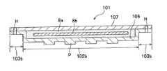
図6に示すように、この微細構造転写モールド1bは、表面層6と、この表面層6と向き合うように配置された基材層7とを備えている。
なお、この微細構造転写モールド1bの平面形状は円形となっているが、第1の実施形態に係る微細構造転写モールド1aと同様に、その平面形状に制限はなく、例えば、楕円形や多角形等であってもよい。
<Microstructure transfer mold>
As shown in FIG. 6, the microstructure transfer mold 1 b includes asurface layer 6 and abase material layer 7 disposed so as to face thesurface layer 6.
Although the planar shape of the microstructure transfer mold 1b is circular, the planar shape is not limited as in themicrostructure transfer mold 1a according to the first embodiment. For example, an elliptical shape or a polygonal shape is used. Etc.

表面層6は、表面に微細な凹凸からなる微細パターンPが形成されたパターン部2bと、このパターン部2bの外側、つまり微細構造転写モールド1bの周縁部に形成された固定部3bとを備えている。微細パターンPは、ナノメータオーダの微細な凹凸で構成されているが、ここで図示する凹凸は、作図の便宜上実寸よりも大幅に拡大して記載している。
そして、表面層6は、パターン部2bと固定部3bとの間に、パターン部2bが固定部3bよりも突出するように傾斜部4bが設けられている。この傾斜部4bは、固定部3bとパターン部2bとの間に段差を設けている。また、パターン部2bと傾斜部4bとは、曲面5bを介してなだらかに連続している。
Thesurface layer 6 includes apattern portion 2b in which a fine pattern P having fine irregularities is formed on the surface, and a fixingportion 3b formed on the outside of thepattern portion 2b, that is, on the peripheral portion of the microstructure transfer mold 1b. ing. The fine pattern P is composed of fine irregularities on the order of nanometers, but the irregularities shown here are shown greatly enlarged for the convenience of drawing.
Thesurface layer 6 is provided with aninclined portion 4b between thepattern portion 2b and the fixedportion 3b so that thepattern portion 2b protrudes from the fixedportion 3b. Theinclined portion 4b is provided with a step between the fixedportion 3b and thepattern portion 2b. Moreover, thepattern part 2b and theinclination part 4b are continuing smoothly via thecurved surface 5b.

このような表面層6の材料としては、第1の実施形態に係る微細構造転写モールド1aの材料と同様のものが挙げられる。  Examples of the material for thesurface layer 6 include the same materials as those for themicrostructure transfer mold 1a according to the first embodiment.

基材層7は、平坦な層であって、前記したように表面層6と向き合うように配置されることで、表面層6との間に放熱性充填物8aとヒータ8bとを内包している。
なお、ここでの放熱性充填物8aは、特許請求の範囲にいう「充填物」に相当し、ヒータ8bは「発熱源」に相当する。
この基材層7は、表面層6のパターン部2bと傾斜部4bとに向き合う基材層本体部7aと、この基材層本体部7aの周囲で表面層6の固定部3bと合わせられて接触する基材層固定部7bとで構成されている。この表面層6の固定部3bと基材層固定部7bとの合わせ部には、固定ブロック15(図1参照)に固定するボルトB(図1参照)を挿通するボルト挿通穴Hが形成されている。
このような基材層7の材料としては、所定の強度と有すると共に要求される精度で加工可能なものであれば特に制限はなく、例えば、ステンレス、アルミ、シリコンのような金属、ガラス、石英、セラミック、プラスチック等が挙げられる。
Thebase material layer 7 is a flat layer, and is disposed so as to face thesurface layer 6 as described above, so that theheat dissipating filler 8a and theheater 8b are included between thesurface layer 6 and thebase material layer 7. Yes.
Here, theheat dissipating filler 8a corresponds to “filling” in the claims, and theheater 8b corresponds to “heat generation source”.
Thebase material layer 7 is combined with the base layer main body portion 7a facing thepattern portion 2b and theinclined portion 4b of thesurface layer 6, and the fixingportion 3b of thesurface layer 6 around the base material layer main body portion 7a. It is comprised with the base material layer fixing |fixed part 7b which contacts. A bolt insertion hole H through which a bolt B (refer to FIG. 1) to be fixed to the fixing block 15 (refer to FIG. 1) is inserted is formed at a joint portion between the fixingportion 3b of thesurface layer 6 and the base materiallayer fixing portion 7b. ing.
The material of thebase material layer 7 is not particularly limited as long as it has a predetermined strength and can be processed with the required accuracy. For example, a metal such as stainless steel, aluminum, silicon, glass, quartz , Ceramic, plastic and the like.

また、基材層7の基材層本体部7aと、基材層固定部7bとは相互に異なる材料で形成されていてもよく、基材層本体部7aの材料としては、基材層本体部7aの弾性率が表面層6の弾性率及び基材層固定部7bの弾性率よりも小さくなるものが望ましく、耐熱性を有するものは更に望ましい。このような基材層本体部7aの材料の具体例としては、例えば、ジメチルシリコーンゴム、フルオロシリコーンゴム、パーフルオロゴム、パーフルオロフォスファーゼンゴムのような合成ゴム、ポリアセタール樹脂、ポリアミド樹脂、ポリフェニレンスルフィド樹脂、シンジオタクチックポリスチレン樹脂、ポリイミド樹脂等のエンジニアリングプラスチックやスーパーエンジニアプラスチック等が挙げられる。また、これらの材料には、更にガラス繊維等の充填材が配合されて使用されてもよい。ちなみに、このような材料で基材層本体部7aが形成されている場合の基材層固定部7bの材料は、前記した基材層7の材料で形成されることとなる。  Moreover, the base material layer main body part 7a and the base materiallayer fixing part 7b of thebase material layer 7 may be formed of mutually different materials. It is desirable that the elastic modulus of the portion 7a is smaller than the elastic modulus of thesurface layer 6 and the elastic modulus of the base materiallayer fixing portion 7b, and it is more desirable to have heat resistance. Specific examples of the material of the base layer main body 7a include, for example, synthetic rubber such as dimethyl silicone rubber, fluorosilicone rubber, perfluoro rubber, perfluorophosphazene rubber, polyacetal resin, polyamide resin, polyphenylene. Examples thereof include engineering plastics such as sulfide resin, syndiotactic polystyrene resin, and polyimide resin, and super engineer plastics. Further, these materials may be used by further blending a filler such as glass fiber. Incidentally, the material of the base materiallayer fixing portion 7b in the case where the base material layer body portion 7a is formed of such a material is formed of the material of thebase material layer 7 described above.

放熱性充填物8aとしては、所定の熱伝導性と耐熱性を有していればよく、例えば、放熱性シリコーンゲル等が挙げられる。また、放熱性充填物8aは、その弾性率が表面層6の弾性率よりも小さいものが望ましい。
ヒータ8bとしては、例えば、抵抗加熱器、誘導加熱器等が挙げられる。ちなみに、ヒータ8bは、第1の実施形態での固定ブロック15に設けられた加熱冷却機構15aの抵抗加熱器と同様に機能する。
Theheat dissipating filler 8a only needs to have predetermined heat conductivity and heat resistance, and examples thereof include heat dissipating silicone gel. Further, it is desirable that theheat dissipating filler 8 a has an elastic modulus smaller than that of thesurface layer 6.
Examples of theheater 8b include a resistance heater and an induction heater. Incidentally, theheater 8b functions similarly to the resistance heater of the heating /cooling mechanism 15a provided in the fixedblock 15 in the first embodiment.

<微細構造転写モールドの製造方法>
次に、この微細構造転写モールド1bの製造方法について説明する。
この製造方法では、図7(a)に示すように、微細パターンPを有するレプリカ22が準備される。このレプリカ22は、図3(c)に示す電気めっきからなるレプリカ22と同様のものであって、微細パターンPの形成面が凸となるように鍛造等の加工が施されたものである。ちなみに、このレプリカ22は、微細構造転写モールド1bの表面層6となる。
次に、図7(b)に示すように、レプリカ22の凹となった側に、ヒータ8bと放熱性充填物8aとが配置される。このヒータ8bは、レプリカ22の凹となった側に放熱性充填物8aで埋設される。
そして、図7(c)に示すように、レプリカ22との間に放熱性充填物8aとヒータ8bとが内包されるように、基材層7が表面層6と向き合うように配置される。その後、表面層6の固定部3bと基材層固定部7bとの合わせ部にボルト挿通穴H(図6参照)が形成されることで図6に示す微細構造転写モールド1bが得られる。
<Production method of microstructure transfer mold>
Next, a method for manufacturing the microstructure transfer mold 1b will be described.
In this manufacturing method, as shown in FIG. 7A, areplica 22 having a fine pattern P is prepared. Thisreplica 22 is the same as thereplica 22 made of electroplating shown in FIG. 3C, and is subjected to processing such as forging so that the formation surface of the fine pattern P becomes convex. Incidentally, thereplica 22 becomes thesurface layer 6 of the microstructure transfer mold 1b.
Next, as shown in FIG. 7B, theheater 8 b and theheat dissipating filler 8 a are arranged on the concave side of thereplica 22. Theheater 8b is embedded with aheat dissipating filler 8a on the concave side of thereplica 22.
Then, as shown in FIG. 7C, thebase material layer 7 is disposed so as to face thesurface layer 6 so that theheat dissipating filler 8 a and theheater 8 b are included between thereplica 22. Thereafter, a bolt insertion hole H (see FIG. 6) is formed in a joint portion between the fixingportion 3b of thesurface layer 6 and the base materiallayer fixing portion 7b, whereby the microstructure transfer mold 1b shown in FIG. 6 is obtained.

このような第2の実施形態に係る微細構造転写モールド1bによれば、前記した第1の実施形態に係る微細構造転写モールド1aと同様の作用効果を奏すると共に、ヒータ8bを備えることで、例えば、図5(b)に示すように、被転写体10の樹脂層10bに微細パターンPを転写する際に、樹脂層10bの温度(T)をより効果的に高めることができる。つまり、微細構造転写モールド1bによれば、樹脂層10bの温度(T)をより効果的に高めることができるので、より速やかに、かつより確実にガラス転移温度(Tg)を上回るように樹脂層10bの温度(T)を設定することができる。  According to the microstructure transfer mold 1b according to the second embodiment as described above, the same effects as themicrostructure transfer mold 1a according to the first embodiment described above can be obtained, and theheater 8b can be provided, for example. As shown in FIG. 5B, the temperature (T) of theresin layer 10b can be more effectively increased when the fine pattern P is transferred to theresin layer 10b of thetransfer target 10. That is, according to the microstructure transfer mold 1b, the temperature (T) of theresin layer 10b can be increased more effectively, so that the resin layer can be more quickly and reliably exceeded the glass transition temperature (Tg). A temperature (T) of 10b can be set.

また、この微細構造転写モールド1bによれば、微細構造転写モールド1bを複数の材料で形成することができるので、微細構造転写モールド1bの特性を部分的に調節することができる。更に具体的に説明すると、例えば、基材層本体部7aの弾性率が、表面層6の弾性率及び基材層固定部7bの弾性率よりも小さくなるような材料を選択した微細構造転写モールド1bは、被転写体10(樹脂層10b)の表面にうねりや反りが生じていても、その被転写体10に対する追従性が向上する。その結果、この微細構造転写モールド1bによれば、被転写体10に対する微細パターンPの転写不良を防止することができる。また、この微細構造転写モールド1bによれば、放熱性充填物8aの弾性率を表面層6の弾性率よりも小さく設定することで、うねりや反りが生じている被転写体10に対しても追従性が向上する。その結果、被転写体10に対する微細パターンPの転写不良を防止することができる。  Further, according to the microstructure transfer mold 1b, the microstructure transfer mold 1b can be formed of a plurality of materials, and therefore the characteristics of the microstructure transfer mold 1b can be partially adjusted. More specifically, for example, a microstructure transfer mold in which a material is selected such that the elastic modulus of the base layer main body portion 7a is smaller than the elastic modulus of thesurface layer 6 and the elastic modulus of the baselayer fixing portion 7b. 1b improves the followability to the transferredobject 10 even if the surface of the transferred object 10 (resin layer 10b) is wavy or warped. As a result, according to the microstructure transfer mold 1b, transfer failure of the fine pattern P to thetransfer target 10 can be prevented. Further, according to the microstructure transfer mold 1b, by setting the elastic modulus of theheat dissipating filler 8a to be smaller than the elastic modulus of thesurface layer 6, it is possible to transfer theobject 10 to which the undulation or warp is generated. Followability is improved. As a result, it is possible to prevent transfer failure of the fine pattern P to thetransfer target 10.

以上、本発明の第1の実施形態及び第2の実施形態について説明したが、本発明はこれらの実施形態に限定されず種々の形態で実施することができる。
前記実施形態では、ステージブロック14を昇降機構13で昇降させることで、被転写体10を微細構造転写モールド1a又は微細構造転写モールド1bに押し当てるようになっているが、本発明は微細構造転写モールド1a又は微細構造転写モールド1bを駆動することで被転写体10に押し当てる駆動装置を備える微細構造転写装置であってもよい。また、本発明の微細構造転写装置は、微細構造転写モールド1a又は微細構造転写モールド1bと、被転写体10との両方を駆動させる駆動装置を備えるものであってもよい。
Although the first embodiment and the second embodiment of the present invention have been described above, the present invention is not limited to these embodiments and can be implemented in various forms.
In the embodiment, the stage block 14 is moved up and down by the elevating mechanism 13 so as to press thetransfer target 10 against themicrostructure transfer mold 1a or the microstructure transfer mold 1b. The microstructure transfer device may include a driving device that presses against thetransfer target 10 by driving themold 1a or the microstructure transfer mold 1b. Further, the fine structure transfer device of the present invention may include a drive device that drives both the finestructure transfer mold 1 a or the fine structure transfer mold 1 b and thetransfer target 10.

前記実施形態では、微細構造転写モールド1a又は微細構造転写モールド1bを固定ブロック15にボルトBで固定するようになっているが、本発明はこれに限定されることなく、クリップ等の他の締結具で固定してもよい。また、本発明ではこれらの締結具による固定と共に、真空吸着や磁力による固定を併用してもよい。  In the embodiment, the finestructure transfer mold 1a or the fine structure transfer mold 1b is fixed to the fixingblock 15 with the bolt B. However, the present invention is not limited to this, and other fastening such as a clip is possible. It may be fixed with tools. Moreover, in this invention, you may use together fixation by vacuum adsorption or magnetic force with fixation by these fasteners.

また、前記実施形態では、被転写体10の樹脂層10bとして熱可塑性樹脂で形成された層を想定しているが、本発明での樹脂層10bは、光硬化性樹脂又は熱硬化性樹脂で形成された層であってもよい。そして、光硬化性樹脂で形成された樹脂層10bに微細パターンPを転写する微細構造転写装置11においては、加熱冷却機構14a,15aに代えて樹脂層10bに光を照射して硬化させる光源が配置されることとなる。  Moreover, in the said embodiment, although the layer formed with the thermoplastic resin was assumed as theresin layer 10b of the to-be-transferred body 10, theresin layer 10b in this invention is a photocurable resin or a thermosetting resin. It may be a formed layer. In the fine structure transfer device 11 that transfers the fine pattern P to theresin layer 10b formed of a photocurable resin, a light source for irradiating theresin layer 10b with light instead of the heating /cooling mechanisms 14a and 15a is cured. Will be placed.

また、前記実施形態では、微細構造転写モールド1a及び微細構造転写モールド1bの製造方法として、原版20から微細パターンPを転写したレプリカ22を使用する方法について説明したが、本発明はパターン部2a,2bに微細パターンPをフォトリソグラフ法等で直接形成したものであってもよい。  In the above embodiment, as a method for manufacturing the finestructure transfer mold 1a and the fine structure transfer mold 1b, the method using thereplica 22 obtained by transferring the fine pattern P from theoriginal plate 20 has been described. The fine pattern P may be directly formed on 2b by a photolithographic method or the like.

また、前記実施形態では、微細構造転写モールド1a及び微細構造転写モールド1bの製造方法として、微細パターンPが転写されたレプリカ22を鍛造等で加工することによってパターン部2a,2bを固定部3a,3bよりも突出させる製造方法について説明しているが、固定部3a,3bよりも突出するパターン部2a,2bを有するレプリカ22を型内で形成する微細構造転写モールド1a及び微細構造転写モールド1bの製造方法であってもよい。ここで参照する図8(a)及び(b)は、固定部よりも突出するパターン部を有するレプリカを型内で形成する形成方法を説明するための工程図である。  Moreover, in the said embodiment, as a manufacturing method of the finestructure transfer mold 1a and the fine structure transfer mold 1b, thepattern part 2a, 2b is processed into the fixing |fixed part 3a, by processing thereplica 22 by which the fine pattern P was transferred by forging etc. Although the manufacturing method which protrudes from 3b is demonstrated, themicrostructure transfer mold 1a and the microstructure transfer mold 1b which form thereplica 22 which haspattern part 2a, 2b which protrudes rather than fixedpart 3a, 3b in a type | mold are demonstrated. It may be a manufacturing method. FIGS. 8A and 8B referred to here are process diagrams for explaining a forming method in which a replica having a pattern portion protruding from a fixed portion is formed in a mold.

ここでのレプリカ22の製造方法は、図8(a)に示すように、まず、上型30aと下型30bとが用意される。これらの上型30aと下型30bとの間には、レプリカ22に対応する形状のキャビティ30cが形成されており、下型30bには微細パターンPが形成されている。
次に、このキャビティ30c内にレプリカ22の材料(図示省略)が配置されると共に、このキャビティ30c内でこの材料が硬化される。
そして、上型30aと下型30bとが取り除かれることで、図8(b)に示すように、微細パターンPを有すると共に固定部3a(3b)よりも突出するパターン部2a(2b)を有するレプリカ22が得られる。
また、図示しないが、プレス成形によって、微細パターンPを形成すると共に、パターン部2a(2b)が突出するように形成することもできる。
In the manufacturing method of thereplica 22 here, as shown in FIG. 8A, first, anupper die 30a and alower die 30b are prepared. Acavity 30c having a shape corresponding to thereplica 22 is formed between theupper mold 30a and thelower mold 30b, and a fine pattern P is formed on thelower mold 30b.
Next, the material of the replica 22 (not shown) is disposed in thecavity 30c, and the material is cured in thecavity 30c.
Then, by removing theupper mold 30a and thelower mold 30b, as shown in FIG. 8B, it has the fine pattern P and thepattern portion 2a (2b) protruding from the fixedportion 3a (3b). Areplica 22 is obtained.
Although not shown, the fine pattern P can be formed by press molding so that thepattern portion 2a (2b) protrudes.

次に、実施例を示しながら本発明をさらに具体的に説明する。
(実施例1)
この実施例1では、図3(a)から(e)に示す工程で微細構造転写モールド1aが製造された。
まず、外径8インチ(20.3cm)のシリコンウエハの表面に、内径が200nmで、深さが300nmのビア(ピット)が複数配置された、微細パターンPを有する原版20(図3(a)参照)が用意された。そして、この原版20の表面には、図示しない無電解ニッケルめっき層を介してニッケルからなる電気めっき層21(図3(a)参照)が形成された。
Next, the present invention will be described more specifically with reference to examples.
Example 1
In Example 1, themicrostructure transfer mold 1a was manufactured by the steps shown in FIGS. 3 (a) to 3 (e).
First, amaster 20 having a fine pattern P (FIG. 3A) in which a plurality of vias (pits) having an inner diameter of 200 nm and a depth of 300 nm are arranged on the surface of a silicon wafer having an outer diameter of 8 inches (20.3 cm). )) Was prepared. Then, anelectroplating layer 21 made of nickel (see FIG. 3A) was formed on the surface of the original 20 via an electroless nickel plating layer (not shown).

なお、無電解ニッケルめっき層は、原版20の表面にアドテック社製のネオガント834を塗布してパラジウム触媒層を形成した後、この原版20を60℃の無電解ニッケルめっき液(奥野製薬工業製のトップケミアロイ66)に3分間浸漬することによって形成した。また、電気めっき層21は、無電解ニッケルめっき層を形成した原版20を50℃のスルファミン酸ニッケルめっき浴に浸漬し、電流密度0.5A/dmで20分間、次いで電流密度1.5A/dmで60分間、更に電流密度3.0A/dmで60分間電鋳を行って形成した。ちなみに、スルファミン酸ニッケルめっき浴は、スルファミン酸ニッケル60%水溶液に、ホウ酸をめっき浴1L当り40g、塩化ニッケルをめっき浴1L当り5g、日本化学工業製のピットレスSをめっき浴1L当り5mL、及び光沢剤(日本化学工業製のNSF−E)を適量混合して調製した。The electroless nickel plating layer was formed by applying a neogant 834 made by Adtech Co. to the surface of theoriginal plate 20 to form a palladium catalyst layer, and then applying theoriginal plate 20 to an electroless nickel plating solution at 60 ° C. (manufactured by Okuno Pharmaceutical Co., Ltd.). It was formed by immersing in top chemialloy 66) for 3 minutes. Theelectroplating layer 21 is obtained by immersing theoriginal plate 20 on which the electroless nickel plating layer is formed in a nickel sulfamate plating bath at 50 ° C. for 20 minutes at a current density of 0.5 A / dm2 and then a current density of 1.5 A / It was formed by performing electroforming at dm2 for 60 minutes and further at a current density of 3.0 A / dm2 for 60 minutes. Incidentally, the nickel sulfamate plating bath is composed of 60% aqueous solution of nickel sulfamate, 40 g of boric acid per liter of plating bath, 5 g of nickel chloride per liter of plating bath, 5 ml of pitless S made by Nippon Chemical Industry, per liter of plating bath, and An appropriate amount of a brightener (NSF-E manufactured by Nippon Chemical Industry Co., Ltd.) was mixed and prepared.

次に、図3(b)に示すように、原版20から電気めっき層21を剥離することで、厚さ100μmのレプリカ22が得られた。  Next, as shown in FIG. 3B, theelectroplating layer 21 was peeled from the original 20 to obtain areplica 22 having a thickness of 100 μm.

そして、図3(c)に示すように、このレプリカ22に鍛造等の加工が施されることで、微細パターンPの形成面が凸となるように、パターン部2a、固定部3a、傾斜部4a及び曲面5aが形成された。パターン部2aの直径は、6インチ(15.2cm)であり、パターン部2aと固定部3aとの段差は、5mmであり、曲面5aの曲率半径は、2.5mmであった。  Then, as shown in FIG. 3C, thereplica 22 is subjected to processing such as forging so that the formation surface of the fine pattern P becomes convex so that thepattern portion 2a, the fixedportion 3a, and the inclined portion are formed. 4a andcurved surface 5a were formed. The diameter of thepattern portion 2a was 6 inches (15.2 cm), the step between thepattern portion 2a and the fixedportion 3a was 5 mm, and the curvature radius of thecurved surface 5a was 2.5 mm.

次に、図3(d)に示すように、レプリカ22の微細パターンPを有する側の面が保護樹脂層27で被覆される共に、これと反対側の面にはニッケルからなる電気めっき層21が更に厚付けされた。保護樹脂層27は、東京応化社製の液状レジストPMERを塗布することによって形成した。電気めっき層21の厚付けは、前記したスルファミン酸ニッケルめっき浴と同じめっき浴が使用された。  Next, as shown in FIG. 3 (d), the surface of thereplica 22 on the side having the fine pattern P is covered with aprotective resin layer 27, and the surface opposite to the surface is covered with anelectroplating layer 21 made of nickel. Was further thickened. Theprotective resin layer 27 was formed by applying a liquid resist PMER manufactured by Tokyo Ohka Co., Ltd. Theelectroplating layer 21 was thickened using the same plating bath as the nickel sulfamate plating bath described above.

そして、図3(e)に示すように、電気めっき層21が厚付けされた側の面(図3(d)の紙面上側の面)が平坦となるように研磨処理が施されると共に固定部3aの所定の位置にボルト挿通穴Hが形成された。その後、保護樹脂層27(図3(d)参照)が除去されることで、微細構造転写モールド1a(図2参照)が得られた。
この微細構造転写モールド1aのパターン部2a(図2参照)の厚さ(微細パターンPの凹凸は測定誤差範囲として考慮せず)は7mmで、固定部3a(図2参照)の厚さは2mmであった。そして、得られた微細構造転写モールド1aの全表面にフッ素系離型剤(ダイキン社製のオプツールDSXの0.5%溶液)を塗布することで離型処理が施された。
Then, as shown in FIG. 3 (e), the surface on which theelectroplating layer 21 is thickened (surface on the upper side of FIG. 3 (d)) is polished and fixed. A bolt insertion hole H was formed at a predetermined position of theportion 3a. Thereafter, the protective resin layer 27 (see FIG. 3D) was removed to obtain themicrostructure transfer mold 1a (see FIG. 2).
The thickness of thepattern portion 2a (see FIG. 2) of themicrostructure transfer mold 1a (the unevenness of the fine pattern P is not considered as a measurement error range) is 7 mm, and the thickness of the fixingportion 3a (see FIG. 2) is 2 mm. Met. And the mold release process was performed by apply | coating a fluorine-type mold release agent (0.5% solution of OPTOOL DSX by Daikin) to the whole surface of the obtainedmicrostructure transfer mold 1a.

次に、得られた微細構造転写モールド1aを組み込んだ図1に示す微細構造転写装置11を使用して、被転写体10に微細パターンP(図2参照)が転写された。この被転写体10には、外径8インチ(20.3cm)のシリコンウエハからなる基板10a上に、樹脂層10bとしての、厚さ1μmのポリスチレン層を形成したものが使用された。  Next, the fine pattern P (see FIG. 2) was transferred to thetransfer target 10 using the fine structure transfer apparatus 11 shown in FIG. 1 incorporating the obtained finestructure transfer mold 1a. Thetransfer body 10 was formed by forming a 1 μm thick polystyrene layer as aresin layer 10b on asubstrate 10a made of a silicon wafer having an outer diameter of 8 inches (20.3 cm).

この微細構造転写装置11(図1参照)を使用した転写方法では、真空チャンバ12内が1kPaまで減圧された後に、加熱冷却機構14a,15aによって、被転写体10(樹脂層10b)及び微細構造転写モールド1aが、150℃に加熱された。
次に、昇降機構13がステージブロック14を上昇させることで、被転写体10が微細構造転写モールド1aに1MPaの圧力で30秒間押し当てられた。その後、加熱冷却機構14a,15aによって、被転写体10(樹脂層10b)及び微細構造転写モールド1aが80℃まで冷却された後、昇降機構13がステージブロック14を降下させることで、被転写体10が微細構造転写モールド1aから離反した。
In the transfer method using the fine structure transfer device 11 (see FIG. 1), after thevacuum chamber 12 is depressurized to 1 kPa, the transferred object 10 (resin layer 10b) and the fine structure are heated by the heating andcooling mechanisms 14a and 15a. Thetransfer mold 1a was heated to 150 ° C.
Next, the elevating mechanism 13 raised the stage block 14 so that thetransfer target 10 was pressed against themicrostructure transfer mold 1a with a pressure of 1 MPa for 30 seconds. After that, the transferred object 10 (resin layer 10b) and the finestructure transfer mold 1a are cooled to 80 ° C. by the heating andcooling mechanisms 14a and 15a, and then the lifting mechanism 13 lowers the stage block 14, thereby transferring the transferred object. 10 separated from themicrostructure transfer mold 1a.

この際、微細構造転写モールド1aから被転写体10が離反するにつれて、ばね部材16bを伸ばしながら、固定ブロック15の他端が軸16a周りに回動した。そして、被転写体10に対して微細構造転写モールド1aが傾斜した結果、軸16a側に剥離起点が生じて被転写体10は微細構造転写モールド1aから容易に剥離した。  At this time, as thetransfer target 10 was separated from themicrostructure transfer mold 1a, the other end of the fixedblock 15 was rotated around theshaft 16a while extending thespring member 16b. Then, as a result of the finestructure transfer mold 1a being inclined with respect to thetransfer target 10, a peeling start point was generated on theshaft 16a side, and thetransfer target 10 was easily peeled from thefine transfer mold 1a.

また、微細構造転写モールド1aから被転写体10が剥離する際に、気体射出機構17のノズル17aから微細構造転写モールド1aの傾斜部4aに向かって高速高圧の窒素ガスが射出された。この窒素ガスは、予めイオナイザ(図示省略)によりイオン化されたものである。その結果、微細構造転写モールド1aからの被転写体10の剥離が促進された。
なお、微細構造転写モールド1aから被転写体10が剥離した後の固定ブロック15は、ばね部材16bの付勢力によって、支持ブロック16側に引き寄せられて元の位置に復元した。
Further, when the transferredobject 10 was peeled from the finestructure transfer mold 1a, high-speed and high-pressure nitrogen gas was injected from thenozzle 17a of thegas injection mechanism 17 toward theinclined portion 4a of the finestructure transfer mold 1a. This nitrogen gas is previously ionized by an ionizer (not shown). As a result, peeling of thetransfer target 10 from themicrostructure transfer mold 1a was promoted.
The fixedblock 15 after the transferredobject 10 was peeled from themicrostructure transfer mold 1a was pulled toward thesupport block 16 by the urging force of thespring member 16b and restored to the original position.

この実施例1では、このような転写工程が、100回繰り返して行われた。その間、微細構造転写装置11においては、微細構造転写モールド1aから被転写体10が剥離する際に、微細構造転写モールド1aが固体ブロック15から脱落することがなく、被転写体10がステージブロック14から脱落することもなかった。
また、転写工程を100回繰り返した後の微細構造転写モールド1aを観察したところ、微細構造転写モールド1aに損傷は認められなかった。
In Example 1, such a transfer process was repeated 100 times. Meanwhile, in the fine structure transfer device 11, the finestructure transfer mold 1a is not dropped from thesolid block 15 when thetransfer target 10 is peeled off from the finestructure transfer mold 1a, and thetransfer target 10 is moved to the stage block 14. It was not dropped out of.
Moreover, when the finestructure transfer mold 1a after observing the transfer process 100 times was observed, no damage was found in the finestructure transfer mold 1a.

(実施例2)
この実施例2では、図4(a)から(f)に示す工程で微細構造転写モールド1aが製造された。
図4(a)に示すレプリカ22は、実施例1のレプリカ22(図3(a)参照)と同様にして作製された。そして、図4(e)に示す母型24の凹部に充填される硬化性樹脂25には、ポリジメチルシロキサン系の液状光硬化性樹脂が使用された。そして、母型24内の硬化性樹脂25は、紫外線を照射されることで硬化して微細構造転写モールド1a(図4(f)参照)を形成した。
そして、この実施例2では、得られた微細構造転写モールド1aを組み込んだ図1に示す微細構造転写装置11を使用して、実施例1と同様に、転写工程が100回繰り返して行われた。その間、微細構造転写装置11においては、微細構造転写モールド1aから被転写体10が剥離する際に、微細構造転写モールド1aが固体ブロック15から脱落することがなく、被転写体10がステージブロック14から脱落することもなかった。
また、転写工程を100回繰り返した後の微細構造転写モールド1aを観察したところ、微細構造転写モールド1aに損傷は認められなかった。
(Example 2)
In Example 2, themicrostructure transfer mold 1a was manufactured by the steps shown in FIGS. 4A to 4F.
Thereplica 22 shown in FIG. 4A was produced in the same manner as thereplica 22 of Example 1 (see FIG. 3A). A polydimethylsiloxane-based liquid photocurable resin was used as thecurable resin 25 filled in the recesses of thematrix 24 shown in FIG. Thecurable resin 25 in thematrix 24 was cured by being irradiated with ultraviolet rays to form themicrostructure transfer mold 1a (see FIG. 4F).
In Example 2, the transfer process was repeated 100 times as in Example 1 using the microstructure transfer apparatus 11 shown in FIG. 1 incorporating the obtainedmicrostructure transfer mold 1a. . Meanwhile, in the fine structure transfer device 11, the finestructure transfer mold 1a is not dropped from thesolid block 15 when thetransfer target 10 is peeled off from the finestructure transfer mold 1a, and thetransfer target 10 is moved to the stage block 14. It was not dropped out of.
Moreover, when the finestructure transfer mold 1a after observing the transfer process 100 times was observed, no damage was found in the finestructure transfer mold 1a.

(実施例3)
この実施例3では、硬化性樹脂25として前記したポリジメチルシロキサン系の液状光硬化性樹脂に代えて、熱硬化型の反応性ポリイミド樹脂(宇部興産製のPETI330)を使用した以外は、実施例2と同様にして微細構造転写モールド1aを製造した。なお、硬化性樹脂25は、2MPaの圧力下に370℃で加熱することで硬化させた。
そして、この実施例3では、得られた微細構造転写モールド1aを組み込んだ図1に示す微細構造転写装置11を使用して、実施例1と同様に、転写工程が100回繰り返して行われた。その間、微細構造転写装置11においては、微細構造転写モールド1aから被転写体10が剥離する際に、微細構造転写モールド1aが固体ブロック15から脱落することがなく、被転写体10がステージブロック14から脱落することもなかった。
また、転写工程を100回繰り返した後の微細構造転写モールド1aを観察したところ、微細構造転写モールド1aに損傷は認められなかった。
(Example 3)
In this Example 3, instead of the polydimethylsiloxane liquid photocurable resin described above as thecurable resin 25, a thermosetting reactive polyimide resin (PET330 made by Ube Industries) was used. In the same manner as in Example 2, amicrostructure transfer mold 1a was produced. Thecurable resin 25 was cured by heating at 370 ° C. under a pressure of 2 MPa.
In Example 3, the transfer process was repeated 100 times as in Example 1 using the microstructure transfer apparatus 11 shown in FIG. 1 incorporating the obtainedmicrostructure transfer mold 1a. . Meanwhile, in the fine structure transfer apparatus 11, when the transferredobject 10 is peeled from the finestructure transfer mold 1a, the finestructure transfer mold 1a is not dropped from thesolid block 15, and the transferredobject 10 is moved to the stage block 14. It was not dropped out of.
Moreover, when the finestructure transfer mold 1a after observing the transfer process 100 times was observed, no damage was found in the finestructure transfer mold 1a.

(実施例4)
この実施例4では、図6に示す微細構造転写モールド1bが製造された。この微細構造転写モールド1bは、図7(a)から(c)に示す工程で製造された。
図7(a)に示すレプリカ22は、実施例1のレプリカ22(図3(c)参照)と同様にして作製された。そして、図7(b)に示す放熱性充填物8aとしては、放熱性シリコーンゲル(モメンティブ・パフォーマンス・マテリアルズ・ジャパン合同会社製のTSE3081)が使用され、ヒータ8bとしては、プレート型ヒータが使用された。また、基材層7としては、厚さ2mmアルミ製が使用された。そして、この実施例4では、放熱性シリコーンゲルを、図7(c)に示すように、ニッケルの電気めっき層からなるレプリカ22(表面層6)とアルミからなる基材層7との間に配置した後に100℃で1時間加熱して硬化させ、図6に示すボルト挿通穴Hを形成することで微細構造転写モールド1bを製造した。
なお、ニッケルの電気めっき層からなる表面層6の弾性率は、約200GPaであった。そして、硬化した放熱性シリコーンゲルからなる放熱性充填物8aは、表面層6の弾性率よりも小さい1MPa以下の弾性率を示すゲル状であった。
そして、この実施例4では、得られた微細構造転写モールド1bを組み込んだ図1に示す微細構造転写装置11を使用して、実施例1と同様に、転写工程が100回繰り返して行われた。その間、微細構造転写装置11においては、微細構造転写モールド1aから被転写体10が剥離する際に、微細構造転写モールド1aが固体ブロック15から脱落することがなく、被転写体10がステージブロック14から脱落することもなかった。そして、放熱性充填物8aの弾性率を表面層6の弾性率よりも小さく設定したことで、微細パターンPの転写不良は認められなかった。
また、転写工程を100回繰り返した後の微細構造転写モールド1aを観察したところ、微細構造転写モールド1aに損傷は認められなかった。
Example 4
In Example 4, the microstructure transfer mold 1b shown in FIG. 6 was manufactured. This microstructure transfer mold 1b was manufactured by the steps shown in FIGS. 7A to 7C.
Areplica 22 shown in FIG. 7A was produced in the same manner as thereplica 22 of Example 1 (see FIG. 3C). As theheat dissipating filler 8a shown in FIG. 7B, a heat dissipating silicone gel (TSE3081 manufactured by Momentive Performance Materials Japan GK) is used, and a plate-type heater is used as theheater 8b. It was done. Further, as thebase material layer 7, aluminum having a thickness of 2 mm was used. And in this Example 4, as shown in FIG.7 (c), heat dissipation silicone gel is made between the replica 22 (surface layer 6) which consists of an electroplating layer of nickel, and thebase material layer 7 which consists of aluminum. After the arrangement, the microstructure transfer mold 1b was manufactured by heating and curing at 100 ° C. for 1 hour to form bolt insertion holes H shown in FIG.
The elastic modulus of thesurface layer 6 made of a nickel electroplating layer was about 200 GPa. Theheat dissipating filler 8a made of the cured heat dissipating silicone gel was in the form of a gel showing an elastic modulus of 1 MPa or less, which is smaller than the elastic modulus of thesurface layer 6.
And in this Example 4, the transfer process was repeated 100 times like Example 1 using the microstructure transfer apparatus 11 shown in FIG. 1 incorporating the obtained microstructure transfer mold 1b. . Meanwhile, in the fine structure transfer device 11, the finestructure transfer mold 1a is not dropped from thesolid block 15 when thetransfer target 10 is peeled off from the finestructure transfer mold 1a, and thetransfer target 10 is moved to the stage block 14. It was not dropped out of. And the transfer defect of the fine pattern P was not recognized by setting the elasticity modulus of theheat dissipation filler 8a smaller than the elasticity modulus of thesurface layer 6.
Moreover, when the finestructure transfer mold 1a after observing the transfer process 100 times was observed, no damage was found in the finestructure transfer mold 1a.

(実施例5)
この実施例5では、図8(a)に示す上型30aと下型30bとの間のキャビティ30c内で、熱硬化型のポリイミド樹脂(宇部興産製のPETI330)を硬化させることで、図8(b)に示すレプリカ22を製造し、このレプリカ22を使用した以外は、実施例4と同様にして図6に示す微細構造転写モールド1bが製造された(図7(a)から(c)参照)。つまり、この実施例5では、ポリイミド樹脂からなる表面層6と、アルミからなる基材層7とを備える微細構造転写モールド1bが製造された。ちなみに、ポリイミド樹脂は、2MPaの圧力下に370℃で加熱することで硬化させた。
なお、下型30bは、実施例2の母型24(図4(d)参照)と同様に製造したものが使用された。また、上型30bは、図6に示す微細構造転写モールド1bの凹部側の形状を模ったものがニッケルの電鋳で製造された。
そして、この実施例5では、得られた微細構造転写モールド1bを組み込んだ図1に示す微細構造転写装置11を使用して、実施例1と同様に、転写工程が100回繰り返して行われた。その間、微細構造転写装置11においては、微細構造転写モールド1aから被転写体10が剥離する際に、微細構造転写モールド1aが固体ブロック15から脱落することがなく、被転写体10がステージブロック14から脱落することもなかった。
また、転写工程を100回繰り返した後の微細構造転写モールド1aを観察したところ、微細構造転写モールド1aに損傷は認められなかった。
(Example 5)
In Example 5, a thermosetting polyimide resin (PET 330 made by Ube Industries) is cured in thecavity 30c between theupper mold 30a and thelower mold 30b shown in FIG. Except that thereplica 22 shown in FIG. 6B was manufactured and thisreplica 22 was used, the microstructure transfer mold 1b shown in FIG. 6 was manufactured in the same manner as in Example 4 (FIGS. 7A to 7C). reference). That is, in Example 5, the microstructure transfer mold 1b including thesurface layer 6 made of polyimide resin and thebase material layer 7 made of aluminum was manufactured. Incidentally, the polyimide resin was cured by heating at 370 ° C. under a pressure of 2 MPa.
In addition, what was manufactured similarly to the mother die 24 (refer FIG.4 (d)) of Example 2 was used for the lower mold |type 30b. Further, theupper mold 30b was manufactured by electroforming nickel with a shape imitating the concave side of the microstructure transfer mold 1b shown in FIG.
In Example 5, the transfer process was repeated 100 times in the same manner as in Example 1 using the microstructure transfer apparatus 11 shown in FIG. 1 incorporating the obtained microstructure transfer mold 1b. . Meanwhile, in the fine structure transfer device 11, the finestructure transfer mold 1a is not dropped from thesolid block 15 when thetransfer target 10 is peeled off from the finestructure transfer mold 1a, and thetransfer target 10 is moved to the stage block 14. It was not dropped out of.
Moreover, when the finestructure transfer mold 1a after observing the transfer process 100 times was observed, no damage was found in the finestructure transfer mold 1a.

(比較例1)
この比較例1では、次の微細構造転写装置を使用して被転写体に転写が行われた。ここで参照する図9は、比較例1で使用した微細構造転写装置の構成説明図である。
図9に示すように、この微細構造転写装置111は、真空チャンバ12内に、昇降機構113で昇降すると共に被転写体110を保持するステージブロック114と、微細構造転写モールド101を固定する固定ブロック115とを備えている。
(Comparative Example 1)
In Comparative Example 1, transfer was performed on the transfer target using the following fine structure transfer device. FIG. 9 referred to here is a configuration explanatory diagram of the fine structure transfer apparatus used in Comparative Example 1. FIG.
As shown in FIG. 9, themicrostructure transfer device 111 includes astage block 114 that moves up and down by alifting mechanism 113 and holds thetransfer target 110 in thevacuum chamber 12, and a fixed block that fixes themicrostructure transfer mold 101. 115.

被転写体110は、基板110aと、この基板110aの表面に積層された樹脂層110bとを備えている。この被転写体110は、昇降機構113でステージブロック114が昇降することで、その樹脂層110bが微細構造転写モールド101に押し当てられ、又はその樹脂層110bが微細構造転写モールド101から離反することとなる。  The transferredobject 110 includes asubstrate 110a and aresin layer 110b laminated on the surface of thesubstrate 110a. In this transferredobject 110, theresin layer 110 b is pressed against themicrostructure transfer mold 101 or theresin layer 110 b is separated from themicrostructure transfer mold 101 when thestage block 114 is moved up and down by thelifting mechanism 113. It becomes.

比較例1での微細構造転写モールド101は、傾斜部4a(図2参照)を有しておらず、微細パターンPが形成される側の面及びその反対側の面がフラット形状となっている。この微細構造転写モールド101は、ニッケルからなる電気めっきで形成されており、固定ブロック115に真空吸着で保持されている。なお、図9中、符号114a及び符号115aは、被転写体110を加熱冷却する加熱冷却機構である。
そして、この比較例1では、この微細構造転写装置111を使用して、被転写体110に転写が行われたが、被転写体110から微細構造転写モールド101を剥離しようとした際に、固定ブロック115から微細構造転写モールド101が脱落した。
Themicrostructure transfer mold 101 in Comparative Example 1 does not have the inclinedportion 4a (see FIG. 2), and the surface on the side on which the fine pattern P is formed and the surface on the opposite side are flat. . Themicrostructure transfer mold 101 is formed by electroplating made of nickel, and is held on the fixedblock 115 by vacuum suction. In FIG. 9,reference numerals 114a and 115a denote heating and cooling mechanisms for heating and cooling thetransfer target 110.
In the first comparative example, the finestructure transfer device 111 was used to perform transfer to thetransfer target 110, but when the finestructure transfer mold 101 was to be peeled from thetransfer target 110, it was fixed. Themicrostructure transfer mold 101 was dropped from theblock 115.

(比較例2)
この比較例2では、次の微細構造転写モールドが製造された。ここで参照する図10は、比較例2で製造した微細構造転写モールドの構成説明図である。
図10に示すように、この微細構造転写モールド101は、表面層106と基材層107との間に放熱性充填物8aとヒータ8bとが配置されている。
そして、この微細構造転写モールド101は、表面層106が傾斜部4a(図2参照)を有しておらず、固定部103bからパターン部102bへの立ち上がりが略直角となっている。つまり、この表面層106は、実施例4の微細構造転写モールド1bの表面層6(図6参照)と異なって、パターン部102bの端に角部が形成されている。
この比較例2での微細構造転写モールド101は、パターン部102bの端に角部が形成されている以外は、実施例4の微細構造転写モールド1bと同様に製造されている。
そして、この比較例2では、得られた微細構造転写モールド101を組み込んだ図1に示す微細構造転写装置11を使用して、実施例1と同様に、転写工程が100回繰り返して行われた。
そして、転写工程を100回繰り返した後の微細構造転写モールド101を観察したところ、パターン部102bの端の角部にクラック状の破断が発生していた。
(Comparative Example 2)
In Comparative Example 2, the following microstructure transfer mold was manufactured. FIG. 10 referred to here is a configuration explanatory view of the microstructure transfer mold manufactured in Comparative Example 2. FIG.
As shown in FIG. 10, in themicrostructure transfer mold 101, aheat dissipating filler 8 a and aheater 8 b are disposed between asurface layer 106 and abase material layer 107.
In themicrostructure transfer mold 101, thesurface layer 106 does not have the inclinedportion 4a (see FIG. 2), and the rising from the fixedportion 103b to thepattern portion 102b is substantially perpendicular. That is, unlike the surface layer 6 (see FIG. 6) of the microstructure transfer mold 1b of Example 4, thesurface layer 106 has corners formed at the ends of thepattern portion 102b.
Themicrostructure transfer mold 101 in Comparative Example 2 is manufactured in the same manner as the microstructure transfer mold 1b of Example 4 except that corners are formed at the ends of thepattern portion 102b.
In Comparative Example 2, the transfer process was repeated 100 times as in Example 1 using the microstructure transfer apparatus 11 shown in FIG. 1 incorporating the obtainedmicrostructure transfer mold 101. .
Then, when themicrostructure transfer mold 101 after the transfer process was repeated 100 times was observed, a crack-like breakage occurred at the corner of the end of thepattern portion 102b.

(実施例及び比較例での微細構造転写モールドの評価)
図9に示すように、比較例1の微細構造転写モールド101は、フラット形状となっているので、例えば、ボルト等の締結具で固定ブロック115に保持させると、微細構造転写モールド101を被転写体110に押し当てる際に、ボルト等の締結具が被転写体110に干渉することとなる。したがって、この比較例1では、この干渉を避けるために、微細構造転写モールド101を固定ブロック115に真空吸着で保持させている。
その結果、この微細構造転写装置111では、固定ブロック115に対する微細構造転写モールド101の保持力が不十分となっている。ちなみに、微細構造転写モールド101をボルト等の締結具で固定ブロック115に保持させると、ボルト等の締結具の被転写体110に対する干渉を避けるために、被転写体110を微細構造転写モールド101よりも小さくする必要がある。
(Evaluation of microstructure transfer molds in Examples and Comparative Examples)
As shown in FIG. 9, themicrostructure transfer mold 101 of Comparative Example 1 has a flat shape. For example, when themicrostructure transfer mold 101 is held on the fixedblock 115 with a fastener such as a bolt, themicrostructure transfer mold 101 is transferred. When pressed against thebody 110, a fastener such as a bolt interferes with the transferredbody 110. Therefore, in this comparative example 1, in order to avoid this interference, the finestructure transfer mold 101 is held on the fixedblock 115 by vacuum suction.
As a result, in the finestructure transfer device 111, the holding force of the finestructure transfer mold 101 with respect to the fixedblock 115 is insufficient. Incidentally, when themicrostructure transfer mold 101 is held on the fixingblock 115 with a fastener such as a bolt, the object to be transferred 110 is removed from themicrostructure transfer mold 101 in order to avoid interference of the fastener such as a bolt with the object to be transferred 110. Need to be smaller.

これに対して、図2及び図6に示すように、実施例1から実施例5の微細構造転写モールド1a,1bは、パターン部2a,2bが固定部3a,3bよりも突出しているので、固定部3a,3bに取り付けたボルトBが被転写体10に干渉することがない。したがって、この微細構造転写モールド1a,1bは、使用可能な被転写体10のサイズが制限されることなく微細構造転写装置11に十分な保持力で保持させることができた。  On the other hand, as shown in FIGS. 2 and 6, in the finestructure transfer molds 1a and 1b of the first to fifth embodiments, thepattern portions 2a and 2b protrude from the fixedportions 3a and 3b. The bolts B attached to the fixingportions 3 a and 3 b do not interfere with thetransfer target 10. Therefore, the finestructure transfer molds 1a and 1b can be held by the fine structure transfer device 11 with a sufficient holding force without limiting the size of thetransfer target 10 that can be used.

そして、比較例2の微細構造転写モールド101は、パターン部102bの端の角部にクラック状の破断が発生した。これは、微細構造転写モールド101対する被転写体110の押し当て及び剥離を繰り返す際に、角部に応力が集中したためと考えられる。  In themicrostructure transfer mold 101 of Comparative Example 2, crack-like breakage occurred at the corner of the end of thepattern portion 102b. This is presumably because stress was concentrated at the corners when theobject 110 to be transferred was repeatedly pressed against and peeled from themicrostructure transfer mold 101.

これに対して、図2及び図6に示すように、実施例1から実施例5の微細構造転写モールド1a,1bは、パターン部2a,2bが固定部3a,3bから突出しており、パターン部2a,2bの端で厚みを稼いでいる。そして、微細構造転写モールド1a,1bは、パターン部2a,2bと傾斜部4a,4bとが、曲面5a,5bでなだらかに連続しているので、前記した応力の集中は確実に防止される。その結果、微細構造転写モールド1a,1bは、パターン部2a,2bの端における破断の発生が防止されて耐久性に優れたものとなった。  On the other hand, as shown in FIGS. 2 and 6, in themicrostructure transfer molds 1a and 1b of the first to fifth embodiments, thepattern portions 2a and 2b protrude from the fixedportions 3a and 3b, and the pattern portion The thickness is gained at the ends of 2a and 2b. In the finestructure transfer molds 1a and 1b, since thepattern portions 2a and 2b and theinclined portions 4a and 4b are smoothly continuous on thecurved surfaces 5a and 5b, the above-described concentration of stress is reliably prevented. As a result, themicrostructure transfer molds 1a and 1b are excellent in durability because the occurrence of breakage at the ends of thepattern portions 2a and 2b is prevented.

第1の実施形態に係る微細構造転写装置の構成説明図である。1 is a configuration explanatory diagram of a microstructure transfer device according to a first embodiment. FIG.図1の微細構造転写装置に組み込まれた微細構造転写モールドの構成説明図である。It is a structure explanatory drawing of the microstructure transfer mold integrated in the microstructure transfer apparatus of FIG.(a)から(e)は、第1の実施形態に係る微細構造転写モールドの製造方法を説明するための工程図である。FIGS. 4A to 4E are process diagrams for explaining a method for manufacturing a microstructure transfer mold according to the first embodiment.(a)から(f)は、第1の実施形態に係る微細構造転写モールドの他の製造方法を説明するための工程図である。FIGS. 4A to 4F are process diagrams for explaining another manufacturing method of the microstructure transfer mold according to the first embodiment.(a)から(d)は、第1の実施形態に係る微細構造転写モールドを使用した転写方法を説明するための工程図である。FIGS. 4A to 4D are process diagrams for explaining a transfer method using the microstructure transfer mold according to the first embodiment.第2の実施形態に係る微細構造転写モールドの構成説明図である。It is composition explanatory drawing of the microstructure transfer mold which concerns on 2nd Embodiment.(a)から(c)は、図6の微細構造転写モールドの製造方法を説明するための工程図である。(A) to (c) is a process diagram for explaining a manufacturing method of the microstructure transfer mold of FIG.(a)及び(b)は、固定部よりも突出するパターン部を有するレプリカを型内で形成する形成方法を説明するための工程図である。(A) And (b) is process drawing for demonstrating the formation method which forms the replica which has a pattern part which protrudes rather than a fixing | fixed part in a type | mold.比較例1で使用した微細構造転写装置の構成説明図である。FIG. 3 is a configuration explanatory diagram of a fine structure transfer device used in Comparative Example 1;比較例2で製造した微細構造転写モールドの構成説明図である。It is a structure explanatory drawing of the microstructure transfer mold manufactured by the comparative example 2.

符号の説明Explanation of symbols

1a 微細構造転写モールド
1b 微細構造転写モールド
2a パターン部
2b パターン部
3a 固定部
3b 固定部
4a 傾斜部
4b 傾斜部
5a 曲面
5b 曲面
6 表面層
7 基材層
7a 基材層本体部
7b 基材層固定部
10 被転写体
10a 基板
10b 樹脂層
11 微細構造転写装置
13 昇降機構(駆動機構)
14 ステージブロック
15 固定ブロック
16a 軸
16b ばね部材
17 気体射出機構
22 レプリカ
P 微細パターン
DESCRIPTION OFSYMBOLS 1a Microstructure transfer mold 1bMicrostructure transfer mold2a Pattern part2b Pattern part3a Fixing part3b Fixing part4a Inclination part4b Inclination part 5aCurved surface 5bCurved surface 6Surface layer 7 Base material layer 7a Base material layermain body part 7b Base materiallayer fixation Part 10Transferobject 10a Substrate 10b Resin layer 11 Fine structure transfer device 13 Lifting mechanism (drive mechanism)
14stage block 15 fixedblock 16a shaft16b spring member 17gas injection mechanism 22 replica P fine pattern

Claims (20)

Translated fromJapanese
表面に微細な凹凸が形成されたパターン部と、
このパターン部の外側に形成された固定部と、
前記パターン部が前記固定部よりも突出するように前記パターン部と前記固定部との間に設けられた傾斜部と、
を備えることを特徴とする微細構造転写モールド。
A pattern portion having fine irregularities formed on the surface;
A fixed portion formed outside the pattern portion;
An inclined portion provided between the pattern portion and the fixed portion so that the pattern portion protrudes from the fixed portion;
A fine structure transfer mold comprising:
前記パターン部と前記傾斜部とは、曲面を介してなだらかに連続していることを特徴とする請求項1に記載の微細構造転写モールド。  The microstructure transfer mold according to claim 1, wherein the pattern portion and the inclined portion are smoothly continuous via a curved surface. ニッケルを主成分とする金属からなることを特徴とする請求項1又は請求項2に記載の微細構造転写モールド。  The microstructure transfer mold according to claim 1 or 2, comprising a metal mainly composed of nickel. 樹脂からなることを特徴とする請求項1又は請求項2に記載の微細構造転写モールド。  The microstructure transfer mold according to claim 1, wherein the microstructure transfer mold is made of a resin. 前記樹脂は、光硬化性樹脂であることを特徴とする請求項4に記載の微細構造転写モールド。  The microstructure transfer mold according to claim 4, wherein the resin is a photocurable resin. 前記樹脂は、ポリイミド樹脂であることを特徴とする請求項4に記載の微細構造転写モールド。  The microstructure transfer mold according to claim 4, wherein the resin is a polyimide resin. 表面に微細な凹凸が形成されたパターン部と、
このパターン部の外側に形成された固定部と、
前記パターン部が前記固定部よりも突出するように前記パターン部と前記固定部との間に設けられた傾斜部と、
を有する表面層を基材層上に備えることを特徴とする微細構造転写モールド。
A pattern portion having fine irregularities formed on the surface;
A fixed portion formed outside the pattern portion;
An inclined portion provided between the pattern portion and the fixed portion so that the pattern portion protrudes from the fixed portion;
A microstructure transfer mold comprising a surface layer having a surface layer on a substrate layer.
前記パターン部と前記傾斜部とは、曲面を介してなだらかに連続していることを特徴とする請求項7に記載の微細構造転写モールド。  The microstructure transfer mold according to claim 7, wherein the pattern part and the inclined part are gently continuous via a curved surface. 前記表面層が、ニッケルを主成分とする金属からなることを特徴とする請求項7又は請求項8に記載の微細構造転写モールド。  The microstructure transfer mold according to claim 7 or 8, wherein the surface layer is made of a metal mainly composed of nickel. 前記表面層が、樹脂からなることを特徴とする請求項7又は請求項8に記載の微細構造転写モールド。  The microstructure transfer mold according to claim 7 or 8, wherein the surface layer is made of a resin. 前記樹脂は、光硬化性樹脂であることを特徴とする請求項10に記載の微細構造転写モールド。  The microstructure transfer mold according to claim 10, wherein the resin is a photocurable resin. 前記樹脂は、ポリイミド樹脂であることを特徴とする請求項10に記載の微細構造転写モールド。  The microstructure transfer mold according to claim 10, wherein the resin is a polyimide resin. 前記基材層が、
前記表面層の前記傾斜部及び前記パターン部に向き合う基材層本体部と、
前記表面層の前記固定部と接触する基材層固定部と、
を有し、
前記基材層本体部の弾性率が、前記表面層の弾性率及び前記基材層固定部の弾性率よりも小さいことを特徴とする請求項7に記載の微細構造転写モールド。
The base material layer is
A base material layer body portion facing the inclined portion and the pattern portion of the surface layer;
A base material layer fixing portion in contact with the fixing portion of the surface layer;
Have
The microstructure transfer mold according to claim 7, wherein an elastic modulus of the base layer main body is smaller than an elastic modulus of the surface layer and an elastic modulus of the base layer fixing part.
前記表面層と前記基材層との間には充填物が配置されており、この充填物の弾性率は、前記表面層の弾性率よりも小さいことを特徴とする請求項7又は請求項8に記載の微細構造転写モールド。  The filling material is arrange | positioned between the said surface layer and the said base material layer, The elastic modulus of this filling material is smaller than the elastic modulus of the said surface layer, The Claim 7 or Claim 8 characterized by the above-mentioned. The microstructure transfer mold according to 1. 前記表面層と前記基材層との間には発熱源が配置されていることを特徴とする請求項7又は請求項8に記載の微細構造転写モールド。  The microstructure transfer mold according to claim 7 or 8, wherein a heat source is disposed between the surface layer and the base material layer. 表面に微細な凹凸が形成されたパターン部と、このパターン部の外側に形成された固定部と、前記パターン部が前記固定部よりも突出するように前記パターン部と前記固定部との間に設けられた傾斜部と、を有する微細構造転写モールドと、
この微細構造転写モールドの前記固定部を固定する固定ブロックと、
被転写体を保持するステージブロックと、
前記微細構造転写モールドと前記被転写体とを接触させた後に離反させるように前記固定ブロック及び前記ステージブロックのうちの少なくとも一方を駆動する駆動機構と、
を備えることを特徴とする微細構造転写装置。
A pattern portion having fine irregularities formed on the surface, a fixing portion formed outside the pattern portion, and the pattern portion and the fixing portion so that the pattern portion protrudes from the fixing portion. A microstructured transfer mold having an inclined portion provided, and
A fixing block for fixing the fixing portion of the microstructure transfer mold;
A stage block for holding the transfer object;
A drive mechanism for driving at least one of the fixed block and the stage block so that the fine structure transfer mold and the transfer target body are separated after being brought into contact with each other;
A fine structure transfer apparatus comprising:
表面に微細な凹凸が形成されたパターン部と、このパターン部の外側に形成された固定部と、前記パターン部が前記固定部よりも突出するように前記パターン部と前記固定部との間に設けられる傾斜部と、を有する表面層が基材層上に形成された微細構造転写モールドと、
この微細構造転写モールドの前記固定部を固定する固定ブロックと、
被転写体を保持するステージブロックと、
前記微細構造転写モールドと前記被転写体とを接触させた後に離反させるように前記微細構造転写モールド及び前記被転写体のうちの少なくとも一方を駆動する駆動機構と、
を備えることを特徴とする微細構造転写装置。
A pattern portion having fine irregularities formed on the surface, a fixing portion formed outside the pattern portion, and the pattern portion and the fixing portion so that the pattern portion protrudes from the fixing portion. A microstructured transfer mold in which a surface layer having a sloped portion is formed on a substrate layer;
A fixing block for fixing the fixing portion of the microstructure transfer mold;
A stage block for holding the transfer object;
A drive mechanism for driving at least one of the microstructure transfer mold and the transferred body so that the microstructure transfer mold and the transfer target body are separated from each other, and
A fine structure transfer apparatus comprising:
前記微細構造転写モールドと前記被転写体とが離反する際に、前記微細構造転写モールドの前記傾斜部に気体を射出する気体射出機構を更に備えることを特徴とする請求項16又は請求項17に記載の微細構造転写装置。  The gas injection mechanism according to claim 16 or 17, further comprising a gas injection mechanism for injecting a gas to the inclined portion of the microstructure transfer mold when the microstructure transfer mold and the transfer target are separated. The microstructure transfer device described. 前記固定ブロックは、その一端が軸で軸支されており、前記微細構造転写モールドと前記被転写体とが離反する際に前記軸周りに回動し、前記微細構造転写モールドが前記被転写体に対して傾斜可能となっていること特徴とする請求項16又は請求項17に記載の微細構造転写装置。  One end of the fixed block is pivotally supported by a shaft, and when the microstructure transfer mold and the transfer object are separated from each other, the fixing block rotates around the axis, and the microstructure transfer mold is moved to the transfer object. The fine structure transfer device according to claim 16 or 17, wherein the fine structure transfer device is capable of tilting with respect to the surface. 前記気体射出機構より射出される前記気体は、荷電粒子を含むことを特徴とする請求項18に記載の微細構造転写装置。  The fine structure transfer apparatus according to claim 18, wherein the gas ejected from the gas ejection mechanism includes charged particles.
JP2008219972A2008-08-282008-08-28 MICROSTRUCTURE TRANSFER MOLD AND MICROSTRUCTURE TRANSFER APPARATUSExpired - Fee RelatedJP5161707B2 (en)

Priority Applications (1)

Application NumberPriority DateFiling DateTitle
JP2008219972AJP5161707B2 (en)2008-08-282008-08-28 MICROSTRUCTURE TRANSFER MOLD AND MICROSTRUCTURE TRANSFER APPARATUS

Applications Claiming Priority (1)

Application NumberPriority DateFiling DateTitle
JP2008219972AJP5161707B2 (en)2008-08-282008-08-28 MICROSTRUCTURE TRANSFER MOLD AND MICROSTRUCTURE TRANSFER APPARATUS

Publications (2)

Publication NumberPublication Date
JP2010052288Atrue JP2010052288A (en)2010-03-11
JP5161707B2 JP5161707B2 (en)2013-03-13

Family

ID=42068720

Family Applications (1)

Application NumberTitlePriority DateFiling Date
JP2008219972AExpired - Fee RelatedJP5161707B2 (en)2008-08-282008-08-28 MICROSTRUCTURE TRANSFER MOLD AND MICROSTRUCTURE TRANSFER APPARATUS

Country Status (1)

CountryLink
JP (1)JP5161707B2 (en)

Cited By (11)

* Cited by examiner, † Cited by third party
Publication numberPriority datePublication dateAssigneeTitle
JP2012006219A (en)*2010-06-242012-01-12Dainippon Printing Co LtdMold for nanoimprint
CN103676472A (en)*2012-09-202014-03-26李永春Pattern transfer substrate device and pattern transfer substrate thereof
CN103717376A (en)*2011-06-022014-04-09Scivax股份有限公司Fluid pressure imprint device and imprint method
KR101499600B1 (en)*2011-01-142015-03-06제이엑스 닛코닛세키 에네루기 가부시키가이샤Method for producing mold for fine pattern transfer, method for producing diffraction grating using same, and method for manufacturing organic el element which comprises the diffraction grating
CN104698743A (en)*2013-12-102015-06-10佳能株式会社Imprint apparatus and method of manufacturing article
JP2015140015A (en)*2014-01-292015-08-03エヌエムテック コリア カンパニー リミテッドMethod for manufacturing panel by high-frequency fusion, and panel manufactured by the method
JP2016048762A (en)*2014-08-282016-04-07株式会社東芝Method for creating pattern data, template, and method for manufacturing semiconductor device
EP3243624A1 (en)*2016-05-132017-11-15Fujifilm CorporationProduction method of mold, manufacturing method of pattern sheet, production method of electroform, production method of mold using electroform, and original
KR20180055464A (en)*2016-11-172018-05-25정연일Manufacturing apparatus for bed panel
CN110033704A (en)*2019-04-192019-07-19京东方科技集团股份有限公司Transfer device and transfer method
CN115976472A (en)*2021-10-152023-04-18南京微纳科技研究院有限公司Apparatus and method for preparing film on substrate

Families Citing this family (1)

* Cited by examiner, † Cited by third party
Publication numberPriority datePublication dateAssigneeTitle
JP6689177B2 (en)2016-11-252020-04-28キオクシア株式会社 Pattern forming method, semiconductor device manufacturing method, and imprint apparatus

Citations (3)

* Cited by examiner, † Cited by third party
Publication numberPriority datePublication dateAssigneeTitle
JP2006035547A (en)*2004-07-262006-02-09Japan Steel Works Ltd:The Method and apparatus for producing molded body
JP2006175756A (en)*2004-12-222006-07-06Hitachi Maxell Ltd Manufacturing method of molded products
JP2007305944A (en)*2006-05-152007-11-22Univ WasedaTransfer device and transfer method

Patent Citations (3)

* Cited by examiner, † Cited by third party
Publication numberPriority datePublication dateAssigneeTitle
JP2006035547A (en)*2004-07-262006-02-09Japan Steel Works Ltd:The Method and apparatus for producing molded body
JP2006175756A (en)*2004-12-222006-07-06Hitachi Maxell Ltd Manufacturing method of molded products
JP2007305944A (en)*2006-05-152007-11-22Univ WasedaTransfer device and transfer method

Cited By (18)

* Cited by examiner, † Cited by third party
Publication numberPriority datePublication dateAssigneeTitle
JP2012006219A (en)*2010-06-242012-01-12Dainippon Printing Co LtdMold for nanoimprint
KR101499600B1 (en)*2011-01-142015-03-06제이엑스 닛코닛세키 에네루기 가부시키가이샤Method for producing mold for fine pattern transfer, method for producing diffraction grating using same, and method for manufacturing organic el element which comprises the diffraction grating
US9291754B2 (en)2011-01-142016-03-22Jx Nippon Oil & Energy CorporationMethod for producing mold for minute pattern transfer, method for producing diffraction grating using the same, and method for producing organic EL element including the diffraction grating
CN103717376A (en)*2011-06-022014-04-09Scivax股份有限公司Fluid pressure imprint device and imprint method
CN103676472A (en)*2012-09-202014-03-26李永春Pattern transfer substrate device and pattern transfer substrate thereof
KR101520182B1 (en)2012-09-202015-05-13내셔널 청쿵 유니버시티Pattern-transferring substrate apparatus and pattern-transferring substrate thereof
US10067420B2 (en)2013-12-102018-09-04Canon Kabushiki KaishaImprint apparatus and method of manufacturing article
CN104698743A (en)*2013-12-102015-06-10佳能株式会社Imprint apparatus and method of manufacturing article
KR101765373B1 (en)*2013-12-102017-08-07캐논 가부시끼가이샤Imprint apparatus and method of manufacturing article
CN104698743B (en)*2013-12-102019-08-16佳能株式会社The method of imprinting apparatus and manufacture article
JP2015140015A (en)*2014-01-292015-08-03エヌエムテック コリア カンパニー リミテッドMethod for manufacturing panel by high-frequency fusion, and panel manufactured by the method
JP2016048762A (en)*2014-08-282016-04-07株式会社東芝Method for creating pattern data, template, and method for manufacturing semiconductor device
US9971342B2 (en)2014-08-282018-05-15Toshiba Memory CorporationPattern data creating method, template, and semiconductor device manufacturing method
EP3243624A1 (en)*2016-05-132017-11-15Fujifilm CorporationProduction method of mold, manufacturing method of pattern sheet, production method of electroform, production method of mold using electroform, and original
KR20180055464A (en)*2016-11-172018-05-25정연일Manufacturing apparatus for bed panel
KR102060561B1 (en)2016-11-172020-02-11정연일Manufacturing apparatus for bed panel
CN110033704A (en)*2019-04-192019-07-19京东方科技集团股份有限公司Transfer device and transfer method
CN115976472A (en)*2021-10-152023-04-18南京微纳科技研究院有限公司Apparatus and method for preparing film on substrate

Also Published As

Publication numberPublication date
JP5161707B2 (en)2013-03-13

Similar Documents

PublicationPublication DateTitle
JP5161707B2 (en) MICROSTRUCTURE TRANSFER MOLD AND MICROSTRUCTURE TRANSFER APPARATUS
JP5117318B2 (en) Nanoimprinting stamper and fine structure transfer apparatus using the stamper
JP5002422B2 (en) Resin stamper for nanoprint
JP4340086B2 (en) Nanoprinting stamper and fine structure transfer method
CN100584636C (en) Nano-printing mold, manufacturing method thereof, nano-printing device and method
JP4467611B2 (en) Optical imprint method
JP5411557B2 (en) Microstructure transfer device
US8535035B2 (en)Fine-structure transfer apparatus
JP4226067B2 (en) Modeling method, lens manufacturing method, and modeling apparatus
JPWO2008126312A1 (en) Thermal imprint apparatus and thermal imprint method
WO2007099907A1 (en)Imprinting mold and method of imprinting
JPWO2008142784A1 (en) Imprint device
JP2008012844A (en) Fine structure transfer apparatus and fine structure transfer method
JP5383110B2 (en) Imprint device
CN105584030B (en)Method for stamping, Embosser, molds and products manufacturing method
JP5062781B2 (en) Imprint method and apparatus using ultrasonic vibration
US8021141B2 (en)Imprint apparatus
JPWO2005057634A1 (en) Pattern formation method using nanoimprint and apparatus for executing the method
JPWO2004093171A1 (en) Pattern forming apparatus and pattern forming method
CN103522165B (en)The manufacture method of grinding pad mould, grinding pad mould and grinding pad
JP2005186557A (en) Pattern forming device, mold holding head
TW202134168A (en)Device and method for embossing micro- and/or nanostructures
JP2006142711A (en) Processing method, processing apparatus, and fine structure manufactured by the method
CN104730859A (en)Imprint method, imprint apparatus, and production method for article
JP4944158B2 (en) Nanoprinting stamper and fine structure transfer method

Legal Events

DateCodeTitleDescription
A621Written request for application examination

Free format text:JAPANESE INTERMEDIATE CODE: A621

Effective date:20100316

A977Report on retrieval

Free format text:JAPANESE INTERMEDIATE CODE: A971007

Effective date:20120330

A131Notification of reasons for refusal

Free format text:JAPANESE INTERMEDIATE CODE: A131

Effective date:20120911

A521Request for written amendment filed

Free format text:JAPANESE INTERMEDIATE CODE: A523

Effective date:20121107

TRDDDecision of grant or rejection written
A01Written decision to grant a patent or to grant a registration (utility model)

Free format text:JAPANESE INTERMEDIATE CODE: A01

Effective date:20121204

A61First payment of annual fees (during grant procedure)

Free format text:JAPANESE INTERMEDIATE CODE: A61

Effective date:20121214

R150Certificate of patent or registration of utility model

Free format text:JAPANESE INTERMEDIATE CODE: R150

FPAYRenewal fee payment (event date is renewal date of database)

Free format text:PAYMENT UNTIL: 20151221

Year of fee payment:3

LAPSCancellation because of no payment of annual fees

[8]ページ先頭

©2009-2025 Movatter.jp