JP2010050177A - Semiconductor device - Google Patents
Semiconductor deviceDownload PDFInfo
- Publication number
- JP2010050177A JP2010050177AJP2008211317AJP2008211317AJP2010050177AJP 2010050177 AJP2010050177 AJP 2010050177AJP 2008211317 AJP2008211317 AJP 2008211317AJP 2008211317 AJP2008211317 AJP 2008211317AJP 2010050177 AJP2010050177 AJP 2010050177A
- Authority
- JP
- Japan
- Prior art keywords
- semiconductor device
- bonding pad
- insulating film
- semiconductor element
- region
- Prior art date
- Legal status (The legal status is an assumption and is not a legal conclusion. Google has not performed a legal analysis and makes no representation as to the accuracy of the status listed.)
- Pending
Links
Images


Classifications
- H—ELECTRICITY
- H01—ELECTRIC ELEMENTS
- H01L—SEMICONDUCTOR DEVICES NOT COVERED BY CLASS H10
- H01L24/00—Arrangements for connecting or disconnecting semiconductor or solid-state bodies; Methods or apparatus related thereto
- H01L24/01—Means for bonding being attached to, or being formed on, the surface to be connected, e.g. chip-to-package, die-attach, "first-level" interconnects; Manufacturing methods related thereto
- H01L24/02—Bonding areas ; Manufacturing methods related thereto
- H01L24/04—Structure, shape, material or disposition of the bonding areas prior to the connecting process
- H01L24/05—Structure, shape, material or disposition of the bonding areas prior to the connecting process of an individual bonding area
- H—ELECTRICITY
- H01—ELECTRIC ELEMENTS
- H01L—SEMICONDUCTOR DEVICES NOT COVERED BY CLASS H10
- H01L2224/00—Indexing scheme for arrangements for connecting or disconnecting semiconductor or solid-state bodies and methods related thereto as covered by H01L24/00
- H01L2224/01—Means for bonding being attached to, or being formed on, the surface to be connected, e.g. chip-to-package, die-attach, "first-level" interconnects; Manufacturing methods related thereto
- H01L2224/02—Bonding areas; Manufacturing methods related thereto
- H01L2224/0212—Auxiliary members for bonding areas, e.g. spacers
- H01L2224/02122—Auxiliary members for bonding areas, e.g. spacers being formed on the semiconductor or solid-state body
- H01L2224/02163—Auxiliary members for bonding areas, e.g. spacers being formed on the semiconductor or solid-state body on the bonding area
- H01L2224/02165—Reinforcing structures
- H01L2224/02166—Collar structures
- H—ELECTRICITY
- H01—ELECTRIC ELEMENTS
- H01L—SEMICONDUCTOR DEVICES NOT COVERED BY CLASS H10
- H01L2224/00—Indexing scheme for arrangements for connecting or disconnecting semiconductor or solid-state bodies and methods related thereto as covered by H01L24/00
- H01L2224/01—Means for bonding being attached to, or being formed on, the surface to be connected, e.g. chip-to-package, die-attach, "first-level" interconnects; Manufacturing methods related thereto
- H01L2224/02—Bonding areas; Manufacturing methods related thereto
- H01L2224/04—Structure, shape, material or disposition of the bonding areas prior to the connecting process
- H01L2224/04042—Bonding areas specifically adapted for wire connectors, e.g. wirebond pads
- H—ELECTRICITY
- H01—ELECTRIC ELEMENTS
- H01L—SEMICONDUCTOR DEVICES NOT COVERED BY CLASS H10
- H01L2224/00—Indexing scheme for arrangements for connecting or disconnecting semiconductor or solid-state bodies and methods related thereto as covered by H01L24/00
- H01L2224/01—Means for bonding being attached to, or being formed on, the surface to be connected, e.g. chip-to-package, die-attach, "first-level" interconnects; Manufacturing methods related thereto
- H01L2224/02—Bonding areas; Manufacturing methods related thereto
- H01L2224/04—Structure, shape, material or disposition of the bonding areas prior to the connecting process
- H01L2224/05—Structure, shape, material or disposition of the bonding areas prior to the connecting process of an individual bonding area
- H01L2224/05001—Internal layers
- H01L2224/05075—Plural internal layers
- H01L2224/0508—Plural internal layers being stacked
- H01L2224/05085—Plural internal layers being stacked with additional elements, e.g. vias arrays, interposed between the stacked layers
- H01L2224/05089—Disposition of the additional element
- H01L2224/05093—Disposition of the additional element of a plurality of vias
- H—ELECTRICITY
- H01—ELECTRIC ELEMENTS
- H01L—SEMICONDUCTOR DEVICES NOT COVERED BY CLASS H10
- H01L2224/00—Indexing scheme for arrangements for connecting or disconnecting semiconductor or solid-state bodies and methods related thereto as covered by H01L24/00
- H01L2224/01—Means for bonding being attached to, or being formed on, the surface to be connected, e.g. chip-to-package, die-attach, "first-level" interconnects; Manufacturing methods related thereto
- H01L2224/42—Wire connectors; Manufacturing methods related thereto
- H01L2224/44—Structure, shape, material or disposition of the wire connectors prior to the connecting process
- H01L2224/45—Structure, shape, material or disposition of the wire connectors prior to the connecting process of an individual wire connector
- H01L2224/45001—Core members of the connector
- H01L2224/45099—Material
- H01L2224/451—Material with a principal constituent of the material being a metal or a metalloid, e.g. boron (B), silicon (Si), germanium (Ge), arsenic (As), antimony (Sb), tellurium (Te) and polonium (Po), and alloys thereof
- H01L2224/45138—Material with a principal constituent of the material being a metal or a metalloid, e.g. boron (B), silicon (Si), germanium (Ge), arsenic (As), antimony (Sb), tellurium (Te) and polonium (Po), and alloys thereof the principal constituent melting at a temperature of greater than or equal to 950°C and less than 1550°C
- H01L2224/45144—Gold (Au) as principal constituent
- H—ELECTRICITY
- H01—ELECTRIC ELEMENTS
- H01L—SEMICONDUCTOR DEVICES NOT COVERED BY CLASS H10
- H01L2224/00—Indexing scheme for arrangements for connecting or disconnecting semiconductor or solid-state bodies and methods related thereto as covered by H01L24/00
- H01L2224/01—Means for bonding being attached to, or being formed on, the surface to be connected, e.g. chip-to-package, die-attach, "first-level" interconnects; Manufacturing methods related thereto
- H01L2224/42—Wire connectors; Manufacturing methods related thereto
- H01L2224/47—Structure, shape, material or disposition of the wire connectors after the connecting process
- H01L2224/48—Structure, shape, material or disposition of the wire connectors after the connecting process of an individual wire connector
- H01L2224/484—Connecting portions
- H01L2224/48463—Connecting portions the connecting portion on the bonding area of the semiconductor or solid-state body being a ball bond
- H—ELECTRICITY
- H01—ELECTRIC ELEMENTS
- H01L—SEMICONDUCTOR DEVICES NOT COVERED BY CLASS H10
- H01L2224/00—Indexing scheme for arrangements for connecting or disconnecting semiconductor or solid-state bodies and methods related thereto as covered by H01L24/00
- H01L2224/01—Means for bonding being attached to, or being formed on, the surface to be connected, e.g. chip-to-package, die-attach, "first-level" interconnects; Manufacturing methods related thereto
- H01L2224/42—Wire connectors; Manufacturing methods related thereto
- H01L2224/47—Structure, shape, material or disposition of the wire connectors after the connecting process
- H01L2224/48—Structure, shape, material or disposition of the wire connectors after the connecting process of an individual wire connector
- H01L2224/485—Material
- H01L2224/48505—Material at the bonding interface
- H01L2224/48599—Principal constituent of the connecting portion of the wire connector being Gold (Au)
- H—ELECTRICITY
- H01—ELECTRIC ELEMENTS
- H01L—SEMICONDUCTOR DEVICES NOT COVERED BY CLASS H10
- H01L2224/00—Indexing scheme for arrangements for connecting or disconnecting semiconductor or solid-state bodies and methods related thereto as covered by H01L24/00
- H01L2224/80—Methods for connecting semiconductor or other solid state bodies using means for bonding being attached to, or being formed on, the surface to be connected
- H01L2224/85—Methods for connecting semiconductor or other solid state bodies using means for bonding being attached to, or being formed on, the surface to be connected using a wire connector
- H01L2224/85009—Pre-treatment of the connector or the bonding area
- H—ELECTRICITY
- H01—ELECTRIC ELEMENTS
- H01L—SEMICONDUCTOR DEVICES NOT COVERED BY CLASS H10
- H01L2924/00—Indexing scheme for arrangements or methods for connecting or disconnecting semiconductor or solid-state bodies as covered by H01L24/00
- H01L2924/01—Chemical elements
- H01L2924/01004—Beryllium [Be]
- H—ELECTRICITY
- H01—ELECTRIC ELEMENTS
- H01L—SEMICONDUCTOR DEVICES NOT COVERED BY CLASS H10
- H01L2924/00—Indexing scheme for arrangements or methods for connecting or disconnecting semiconductor or solid-state bodies as covered by H01L24/00
- H01L2924/01—Chemical elements
- H01L2924/01006—Carbon [C]
- H—ELECTRICITY
- H01—ELECTRIC ELEMENTS
- H01L—SEMICONDUCTOR DEVICES NOT COVERED BY CLASS H10
- H01L2924/00—Indexing scheme for arrangements or methods for connecting or disconnecting semiconductor or solid-state bodies as covered by H01L24/00
- H01L2924/01—Chemical elements
- H01L2924/01013—Aluminum [Al]
- H—ELECTRICITY
- H01—ELECTRIC ELEMENTS
- H01L—SEMICONDUCTOR DEVICES NOT COVERED BY CLASS H10
- H01L2924/00—Indexing scheme for arrangements or methods for connecting or disconnecting semiconductor or solid-state bodies as covered by H01L24/00
- H01L2924/01—Chemical elements
- H01L2924/01014—Silicon [Si]
- H—ELECTRICITY
- H01—ELECTRIC ELEMENTS
- H01L—SEMICONDUCTOR DEVICES NOT COVERED BY CLASS H10
- H01L2924/00—Indexing scheme for arrangements or methods for connecting or disconnecting semiconductor or solid-state bodies as covered by H01L24/00
- H01L2924/01—Chemical elements
- H01L2924/01015—Phosphorus [P]
- H—ELECTRICITY
- H01—ELECTRIC ELEMENTS
- H01L—SEMICONDUCTOR DEVICES NOT COVERED BY CLASS H10
- H01L2924/00—Indexing scheme for arrangements or methods for connecting or disconnecting semiconductor or solid-state bodies as covered by H01L24/00
- H01L2924/01—Chemical elements
- H01L2924/01018—Argon [Ar]
- H—ELECTRICITY
- H01—ELECTRIC ELEMENTS
- H01L—SEMICONDUCTOR DEVICES NOT COVERED BY CLASS H10
- H01L2924/00—Indexing scheme for arrangements or methods for connecting or disconnecting semiconductor or solid-state bodies as covered by H01L24/00
- H01L2924/01—Chemical elements
- H01L2924/01033—Arsenic [As]
- H—ELECTRICITY
- H01—ELECTRIC ELEMENTS
- H01L—SEMICONDUCTOR DEVICES NOT COVERED BY CLASS H10
- H01L2924/00—Indexing scheme for arrangements or methods for connecting or disconnecting semiconductor or solid-state bodies as covered by H01L24/00
- H01L2924/01—Chemical elements
- H01L2924/01079—Gold [Au]
- H—ELECTRICITY
- H01—ELECTRIC ELEMENTS
- H01L—SEMICONDUCTOR DEVICES NOT COVERED BY CLASS H10
- H01L2924/00—Indexing scheme for arrangements or methods for connecting or disconnecting semiconductor or solid-state bodies as covered by H01L24/00
- H01L2924/049—Nitrides composed of metals from groups of the periodic table
- H01L2924/0504—14th Group
- H01L2924/05042—Si3N4
- H—ELECTRICITY
- H01—ELECTRIC ELEMENTS
- H01L—SEMICONDUCTOR DEVICES NOT COVERED BY CLASS H10
- H01L2924/00—Indexing scheme for arrangements or methods for connecting or disconnecting semiconductor or solid-state bodies as covered by H01L24/00
- H01L2924/10—Details of semiconductor or other solid state devices to be connected
- H01L2924/11—Device type
- H01L2924/14—Integrated circuits
- H—ELECTRICITY
- H01—ELECTRIC ELEMENTS
- H01L—SEMICONDUCTOR DEVICES NOT COVERED BY CLASS H10
- H01L2924/00—Indexing scheme for arrangements or methods for connecting or disconnecting semiconductor or solid-state bodies as covered by H01L24/00
- H01L2924/19—Details of hybrid assemblies other than the semiconductor or other solid state devices to be connected
- H01L2924/1901—Structure
- H01L2924/1904—Component type
- H01L2924/19043—Component type being a resistor
- H—ELECTRICITY
- H01—ELECTRIC ELEMENTS
- H01L—SEMICONDUCTOR DEVICES NOT COVERED BY CLASS H10
- H01L2924/00—Indexing scheme for arrangements or methods for connecting or disconnecting semiconductor or solid-state bodies as covered by H01L24/00
- H01L2924/30—Technical effects
- H01L2924/301—Electrical effects
- H01L2924/30105—Capacitance
Landscapes
- Engineering & Computer Science (AREA)
- Computer Hardware Design (AREA)
- Microelectronics & Electronic Packaging (AREA)
- Power Engineering (AREA)
- Internal Circuitry In Semiconductor Integrated Circuit Devices (AREA)
- Semiconductor Integrated Circuits (AREA)
- Wire Bonding (AREA)
Abstract
Translated fromJapaneseDescription
Translated fromJapaneseこの発明は、半導体装置に関し、特に、半導体素子部と重なるように配置されたボンディングパッド部を備えた半導体装置に関する。 The present invention relates to a semiconductor device, and more particularly, to a semiconductor device including a bonding pad portion arranged so as to overlap a semiconductor element portion.
半導体装置は、搭載される電子機器の高機能化および高性能化の進展に伴い、集積度(1つのチップ上に集積された半導体素子部の数)が増大し、チップサイズが大きくなる傾向にある。一方で、半導体装置を搭載したパッケージの小型化が求められ、加工寸法の微細化(デザインルールの縮小化)や、パッケージの小型化等によるチップサイズの小型化が行われている。電源用ICなどの半導体装置は、汎用デバイスである事などから他社とのベンチマーク、技術競争およびコスト競争が激しい分野であり、低コスト化のためのチップサイズの小型化およびパッケージの小型化が、特に重要である。 With the progress of higher functionality and higher performance of electronic devices mounted on semiconductor devices, the degree of integration (number of semiconductor element parts integrated on one chip) increases and the chip size tends to increase. is there. On the other hand, downsizing of a package on which a semiconductor device is mounted is required, and downsizing of a chip size is performed by miniaturization of processing dimensions (reduction of design rules), downsizing of a package, and the like. Semiconductor devices such as ICs for power supply are fields where benchmarks with other companies, technology competition and cost competition are intense because they are general-purpose devices, etc. Chip size reduction and package size reduction for cost reduction, Of particular importance.
半導体装置のチップは、チップ内部の動作領域(活性領域と呼ばれることもある)と、チップ表面に形成されるボンディングパッド領域とに大別出来る。動作領域は、トランジスタや抵抗体等の半導体素子部が形成された領域(活性領域)と、半導体素子部間を繋ぐ金属配線層が形成された領域(配線領域)とを含んでいる。 A chip of a semiconductor device can be roughly divided into an operation area (sometimes called an active area) inside the chip and a bonding pad area formed on the chip surface. The operation region includes a region (active region) where a semiconductor element portion such as a transistor or a resistor is formed, and a region (wiring region) where a metal wiring layer connecting between the semiconductor element portions is formed.
ボンディングパッド領域は、ボンディングパッドが形成される領域である。ボンディングパッドは、半導体装置の信号の入出力などのために、例えば金の細線(ボンディングワイヤー)を用いたワイヤーボンディング等により外部と電気的に接続される接続用の電極である。通常、ボンディングパッドは、活性領域と重なる領域を避けてチップの周縁部に設けられている。これは、ワイヤーボンディング等のボンディングを行う際に、ボンディングパッドに加わる荷重や圧力等が、半導体素子部が形成された活性領域に印加されないようにするためである。 The bonding pad region is a region where bonding pads are formed. The bonding pad is a connection electrode that is electrically connected to the outside, for example, by wire bonding using a gold thin wire (bonding wire) for input / output of signals of the semiconductor device. Usually, the bonding pad is provided on the peripheral edge of the chip, avoiding the area overlapping the active area. This is to prevent a load or pressure applied to the bonding pad from being applied to the active region in which the semiconductor element portion is formed when bonding such as wire bonding is performed.
また、かつては、半導体素子部間を繋ぐ金属配線層は1層で充分であったが、機能・性能の向上、および、集積度の増大に伴って、金属配線層が複雑かつ長くなり、信号が正しく伝送されない等の不都合が生じていた。 In the past, a single metal wiring layer was sufficient to connect the semiconductor element parts. However, as the function and performance improved and the degree of integration increased, the metal wiring layer became more complicated and longer. Inconveniences such as not being transmitted correctly.
この不都合を解決する方法として、層間絶縁膜を介して複数の金属配線層を積層する多層配線構造が提案された。これにより、金属配線層の自由度が増し、半導体装置の機能・性能の向上、および、集積度の向上が容易に達成できるようになった。 As a method for solving this inconvenience, a multilayer wiring structure in which a plurality of metal wiring layers are stacked via an interlayer insulating film has been proposed. As a result, the degree of freedom of the metal wiring layer is increased, and the function and performance of the semiconductor device and the degree of integration can be easily achieved.
一方、半導体装置の高機能化や高性能化に伴い、その入出力等のためのパッケージの端子数も増えている。ボンディングパッドは、パッケージの端子毎に必要である。このため、ボンディングパッドの数もパッケージの端子数の増加および機能の増加に対応して増加している。このようなボンディングパッドの数の増加に伴い、チップ表面におけるボンディングパッド領域の占める面積が増大している。これにより、半導体装置のチップサイズの小型化ができず、半導体装置を搭載する電子機器の小型化及び低価格化の要請に応えられなくなる。 On the other hand, as the functions and performance of semiconductor devices increase, the number of terminals of the package for input / output of the semiconductor devices also increases. A bonding pad is required for each terminal of the package. For this reason, the number of bonding pads also increases in response to an increase in the number of terminals of the package and an increase in functions. As the number of bonding pads increases, the area occupied by the bonding pad region on the chip surface increases. As a result, the chip size of the semiconductor device cannot be reduced, and it becomes impossible to meet the demands for downsizing and lowering the price of electronic equipment on which the semiconductor device is mounted.
チップサイズを縮小する1つの手法として、従来はチップの活性領域と重なる領域を避けてチップ周縁部に設けられていたボンディングパッドを、チップの活性領域と重なる領域(活性領域の真上の領域)に設ける手法が提案されている。このように、チップの活性領域と重なるように配置されたボンディングパッドは、「エリアパッド」と呼ばれている。 As one technique for reducing the chip size, a bonding pad provided on the peripheral edge of the chip so as to avoid the area overlapping with the active area of the chip is conventionally overlapped with the active area of the chip (the area directly above the active area). A method to be provided in is proposed. Thus, the bonding pad arranged so as to overlap with the active region of the chip is called an “area pad”.
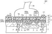
図9は、活性領域と重なるように配置されたボンディングパッド(エリアパッド)を備えた従来の一例による半導体装置の一部の構造を示した断面図である。 FIG. 9 is a cross-sectional view showing a partial structure of a semiconductor device according to an example of the related art provided with bonding pads (area pads) arranged so as to overlap the active region.
従来の一例による半導体装置1001は、図9に示すように、半導体素子部1020が形成された領域である活性領域(動作領域)を含むシリコン基板1002と、シリコン基板1002上に配置され、半導体素子部1020と電気的に接続された配線層1003と、配線層1003上に層間絶縁膜1004を介して配置された配線層1005と、配線層1005と電気的に接続され、少なくとも一部が半導体素子部1020(活性領域)と重なるように配置されたボンディングパッド(エリアパッド)1006とを備えている。 As shown in FIG. 9, a
シリコン基板1002の表面部分には、ソース領域1007と、ドレイン領域1008と、素子分離領域1009とが形成されている。また、シリコン基板1002の上面上には、ゲート絶縁膜1010を介してゲート電極1011が形成されている。そして、ソース領域1007、ドレイン領域1008、ゲート絶縁膜1010およびゲート電極1011によって、MOS(Metal Oxide Semiconductor)トランジスタからなる半導体素子部1020が構成されている。 A source region 1007, a
また、ゲート電極1011および素子分離領域1009を覆うように、絶縁膜1012が形成されている。そして、絶縁膜1012上には、アルミニウムからなる配線層1003が形成されており、配線層1003の一部は、絶縁膜1012のスルーホール1012aを介して半導体素子部1020(ソース領域1007およびドレイン領域1008)に電気的に接続されている。 An
また、配線層1003上には、層間絶縁膜1004が形成されている。この層間絶縁膜1004は、シリコン基板1002側(下側)から順に積層されたシリコン酸化膜1004a、SOG膜1004bおよびシリコン酸化膜1004cによって構成されている。シリコン酸化膜1004aおよびシリコン酸化膜1004cは、例えば、約500nmの厚みに形成されている。また、SOG膜1004bは、配線層1003に起因して発生した表面の凹凸形状を平坦化する機能を有する。 An
層間絶縁膜1004上には、アルミニウムからなる配線層1005が形成されており、配線層1005の一部は、層間絶縁膜1004のスルーホール1004dを介して配線層1003の一部に電気的に接続されている。 A
また、層間絶縁膜1004および配線層1005上に、SiO2膜やSiN膜からなる保護膜1013が形成されている。この保護膜1013には、配線層1005上の所定領域に、開口部1013aが形成されている。また、保護膜1013の表面は、配線層1005に起因して凹凸形状に形成されている。A
また、保護膜1013上の所定領域には、ポリイミド膜1014が形成されている。このポリイミド膜1014には、保護膜1013の開口部1013aに対応する位置(半導体素子部1020の真上の位置)に開口部1014aが形成されている。 A
また、保護膜1013およびポリイミド膜1014上の所定領域には、ボンディングパッド(エリアパッド)1006が形成されている。このボンディングパッド1006は、ポリイミド膜1014の開口部1014aおよび保護膜1013の開口部1013aを介して、配線層1005の一部に電気的に接続されている。 A bonding pad (area pad) 1006 is formed in a predetermined region on the
また、ボンディングパッド1006は、配線層1005、保護膜1013およびポリイミド膜1014に接するように形成されたバリアメタル層1006aと、バリアメタル層1006a上に形成されたAuバンプ(バンプ電極)1006bとによって構成されている。 The
従来の一例による半導体装置1001では、ポリイミド膜1014は、ボンディングパッド1006の中央部から外周部に向かって、厚みが大きくなるように形成されている。すなわち、ポリイミド膜1014の上面は、ボンディングパッド1006の中央部から外周部に向かって傾斜している。 In the
また、ポリイミド膜1014は、配線層1005の所定部分とボンディングパッド1006とを電気的に絶縁する機能を有する。また、ポリイミド膜1014は、ワイヤーボンディングや実装を行う際に、ボンディングパッド1006に加わる荷重や圧力などが、ボンディングパッド1006の真下の領域に伝わるのを抑制するための緩衝材としての機能も有する。 The
なお、半導体装置1001のような構造は、例えば、特許文献1に開示されている。
しかしながら、従来の一例による半導体装置1001では、保護膜1013の表面は配線層1005に起因して凹凸形状に形成されているので、ワイヤーボンディングや実装を行った際に、保護膜1013にボンディングパッド1006から荷重や圧力などが加わり、亀裂が生じる場合がある。保護膜1013に亀裂が生じると、亀裂に水分が浸入し、その部分に電流が流れることにより、配線層1005が腐食したり断線する場合があるという問題点がある。 However, in the
また、ポリイミド膜1014は、ボンディングパッド1006の中央部から外周部に向かって傾斜しているので、ワイヤーボンディングや実装を行う際にボンディングパッド1006に加わる荷重や圧力などが不均一になる。このため、ボンディングワイヤー(金属線)(図示せず)などと、ボンディングパッド1006および配線層1005とを、電気的に良好に接続するのが困難であるという問題点がある。 Further, since the
また、ポリイミド膜1014には、半導体素子部1020の真上の位置に開口部1014aが形成されているので、ワイヤーボンディングや実装を行う際に、開口部1014aの真下の領域に位置する半導体素子部1020に、荷重や圧力などが加わるのを十分に抑制することが困難である。このため、半導体素子部1020にダメージが生じるのを十分に抑制することが困難であるという問題点がある。 In addition, since the opening 1014a is formed in the
なお、ポリイミド膜1014は、有機絶縁膜であるので、バリアメタル層1006a(ボンディングパッド1006)との密着力が比較的低い。このため、バリアメタル層1006a(ボンディングパッド1006)が、外的圧力により、ポリイミド膜1014との界面で剥がれてしまう可能性があるという不都合がある。この不都合を回避するために、ポリイミド膜1014を形成しない手法も考えられるが、ボンディングパッド1006から半導体素子部1020に加わる荷重や圧力などを抑制する緩衝材がなくなる。その結果、ワイヤーボンディングや実装を行う際の荷重や圧力などにより、半導体素子部1020のダメージが大きくなる。 Note that since the
この発明は、上記のような課題を解決するためになされたものであり、この発明の目的は、電気的な接続が良好であるとともに、半導体素子部にダメージが生じるのを十分に抑制することが可能な半導体装置を提供することである。 The present invention has been made to solve the above-described problems, and an object of the present invention is to sufficiently suppress the occurrence of damage to the semiconductor element portion as well as good electrical connection. It is an object of the present invention to provide a semiconductor device capable of performing
上記目的を達成するために、この発明の一の局面による半導体装置は、トランジスタおよび抵抗体の少なくとも一方を含む半導体素子部と、複数の金属配線層と、複数の金属配線層の間に配置された層間絶縁膜とを備え、複数の金属配線層のうちの最上層の金属配線層は、ボンディングパッド部を含み、ボンディングパッド部上には、バンプ電極が形成されておらず、ボンディングパッド部は、層間絶縁膜を介して、半導体素子部と重なるように配置され、層間絶縁膜は、少なくともボンディングパッド部の真下の領域、および、半導体素子部の真上の領域に配置される平坦な上面を有する有機絶縁膜を含む。 In order to achieve the above object, a semiconductor device according to an aspect of the present invention is disposed between a semiconductor element portion including at least one of a transistor and a resistor, a plurality of metal wiring layers, and a plurality of metal wiring layers. The uppermost metal wiring layer of the plurality of metal wiring layers includes a bonding pad portion, and no bump electrode is formed on the bonding pad portion. The interlayer insulating film is disposed so as to overlap with the semiconductor element portion via the interlayer insulating film, and the interlayer insulating film has a flat upper surface disposed at least in a region immediately below the bonding pad portion and a region immediately above the semiconductor element portion. Including an organic insulating film.
この一の局面による半導体装置では、上記のように、ボンディングパッド部の真下の領域に、平坦な上面を有する有機絶縁膜を配置することによって、ボンディングパッド部の真下の領域において、層間絶縁膜の表面に凹凸形状が形成されるのを抑制することができる。これにより、ボンディングパッド部にワイヤーボンディングを行う際(ワイヤーボンディング時)に、層間絶縁膜にボンディングパッド部から荷重や圧力などが加わり亀裂が生じるのを抑制することができる。その結果、層間絶縁膜下の金属配線層が腐食したり断線するのを抑制することができるので、半導体素子部とボンディングパッド部とを電気的に良好に接続することができる。 In the semiconductor device according to this aspect, as described above, the organic insulating film having a flat upper surface is disposed in the region directly below the bonding pad portion, so that the interlayer insulating film is formed in the region immediately below the bonding pad portion. It is possible to suppress the formation of irregular shapes on the surface. Thereby, when wire bonding is performed on the bonding pad portion (at the time of wire bonding), it is possible to suppress the occurrence of cracks due to the load or pressure applied to the interlayer insulating film from the bonding pad portion. As a result, it is possible to prevent the metal wiring layer under the interlayer insulating film from being corroded or disconnected, so that the semiconductor element portion and the bonding pad portion can be electrically connected well.
また、一の局面による半導体装置では、上記のように、ボンディングパッド部の真下の領域に、平坦な上面を有する有機絶縁膜を配置することによって、ワイヤーボンディング時に、ボンディングパッド部に荷重や圧力などが不均一に加わるのを抑制することができる。これにより、ボンディングワイヤー(金属線)と金属配線層(ボンディングパッド部)とを、電気的に良好に接続することができる。 Moreover, in the semiconductor device according to one aspect, as described above, by placing an organic insulating film having a flat upper surface in a region directly below the bonding pad portion, a load or a pressure is applied to the bonding pad portion during wire bonding. Can be prevented from being applied non-uniformly. Thereby, a bonding wire (metal wire) and a metal wiring layer (bonding pad part) can be electrically connected favorably.
また、一の局面による半導体装置では、上記のように、半導体素子部の真上の領域に、有機絶縁膜を配置している。有機絶縁膜は、シリコン酸化膜やSOG膜などの無機絶縁膜に比べて弾力性が高いので、半導体素子部の真上の領域にシリコン酸化膜やSOG膜などの無機絶縁膜を配置する場合に比べて、ワイヤーボンディング時に、ボンディングパッド部から半導体素子部に荷重や圧力などが伝わるのを十分に抑制することができる。これにより、半導体素子部にダメージが生じるのを十分に抑制することができる。 In the semiconductor device according to one aspect, as described above, the organic insulating film is disposed in the region directly above the semiconductor element portion. The organic insulating film has higher elasticity than inorganic insulating films such as silicon oxide film and SOG film. Therefore, when an inorganic insulating film such as silicon oxide film and SOG film is disposed in the region directly above the semiconductor element portion. In comparison, it is possible to sufficiently suppress the transmission of a load or pressure from the bonding pad portion to the semiconductor element portion during wire bonding. Thereby, it is possible to sufficiently suppress the semiconductor element portion from being damaged.
上記一の局面による半導体装置において、好ましくは、有機絶縁膜は、ポリイミド膜を含む。このように構成すれば、例えばスピン塗布法などを用いてポリイミド膜を形成することにより、有機絶縁膜の上面を、容易に平坦に形成することができる。また、ポリイミド膜は弾力性に富むので、ワイヤーボンディング時に、ボンディングパッド部から半導体素子部に荷重や圧力など伝わるのを、容易に、抑制することができる。 In the semiconductor device according to the aforementioned aspect, the organic insulating film preferably includes a polyimide film. If comprised in this way, the upper surface of an organic insulating film can be easily formed flat by forming a polyimide film using a spin coating method etc., for example. Further, since the polyimide film is rich in elasticity, it is possible to easily suppress the transmission of load, pressure, etc. from the bonding pad portion to the semiconductor element portion during wire bonding.
上記一の局面による半導体装置において、好ましくは、ボンディングパッド部と有機絶縁膜との間、および、有機絶縁膜と半導体素子部との間の少なくとも一方には、SiN膜が形成されている。このように構成すれば、SiN膜は機械的な強度が比較的高いので、ワイヤーボンディング時に、ボンディングパッド部から半導体素子部に荷重や圧力などが伝わるのをより抑制することができる。これにより、半導体素子部にダメージが生じるのをより十分に抑制することができる。 In the semiconductor device according to the above aspect, an SiN film is preferably formed between at least one of the bonding pad portion and the organic insulating film and between the organic insulating film and the semiconductor element portion. If comprised in this way, since a SiN film | membrane has comparatively high mechanical strength, it can suppress more that a load, a pressure, etc. are transmitted from a bonding pad part to a semiconductor element part at the time of wire bonding. Thereby, it can suppress more fully that a semiconductor element part arises a damage.
上記SiN膜が形成されている半導体装置において、好ましくは、ボンディングパッド部と有機絶縁膜との間に、SiN膜が形成されている。このように構成すれば、ワイヤーボンディング時に、想定以上の荷重や圧力などが印加されてSiN膜が損傷したとしても、SiN膜の真下の領域に位置する有機絶縁膜により、ボンディングパッド部から半導体素子部に荷重や圧力などが伝わるのを抑制することができるとともに、電気的絶縁性を保つことができる。すなわち、SiN膜が損傷しても、半導体装置の電気的特性、品質および信頼性は劣化しない。 In the semiconductor device in which the SiN film is formed, the SiN film is preferably formed between the bonding pad portion and the organic insulating film. If comprised in this way, even if the load or pressure more than assumption was applied at the time of wire bonding and a SiN film was damaged, an organic insulating film located in the area | region directly under a SiN film | membrane will make a semiconductor element from a bonding pad part. It is possible to suppress the load and pressure from being transmitted to the part, and to maintain electrical insulation. That is, even if the SiN film is damaged, the electrical characteristics, quality, and reliability of the semiconductor device are not deteriorated.
上記SiN膜が形成されている半導体装置において、好ましくは、有機絶縁膜と半導体素子部との間に、減圧CVD法を用いて形成されるとともに、半導体素子部の動作に寄与しないSiN膜が形成されている。このように構成すれば、減圧CVD法を用いて形成されたSiN膜は、例えばプラズマCVD法により形成される一般的なSiN膜に比べて、より緻密で、かつ、より機械的な強度が高いので、ワイヤーボンディング時に、ボンディングパッド部から半導体素子部に荷重や圧力などが伝わるのをさらに抑制することができる。これにより、半導体素子部にダメージが生じるのをさらに抑制することができる。また、SiN膜は、半導体素子部の動作に寄与しないので、ワイヤーボンディング時に、想定以上の荷重や圧力などが印加されてSiN膜が損傷したとしても、半導体装置の電気的特性には影響しない。 In the semiconductor device in which the SiN film is formed, preferably, an SiN film is formed between the organic insulating film and the semiconductor element portion by using a low pressure CVD method and does not contribute to the operation of the semiconductor element portion. Has been. With this configuration, the SiN film formed by using the low pressure CVD method is denser and has higher mechanical strength than, for example, a general SiN film formed by the plasma CVD method. Therefore, it is possible to further suppress the transmission of a load or pressure from the bonding pad portion to the semiconductor element portion during wire bonding. Thereby, it is possible to further suppress the semiconductor element portion from being damaged. In addition, since the SiN film does not contribute to the operation of the semiconductor element portion, even if a load or pressure more than expected is applied during wire bonding and the SiN film is damaged, the electrical characteristics of the semiconductor device are not affected.
上記有機絶縁膜と半導体素子部との間にSiN膜が形成されている半導体装置において、好ましくは、SiN膜は、ボンディングパッド部の真下の領域以外の領域で、SiN容量として機能する。このように構成すれば、ボンディングパッド部の真下の領域以外の領域におけるSiN容量の形成と、半導体素子部にダメージが生じるのを抑制するための膜(SiN膜)の形成とを同時に行うことができるので、製造プロセスを簡略化することができる。 In the semiconductor device in which the SiN film is formed between the organic insulating film and the semiconductor element portion, the SiN film preferably functions as a SiN capacitor in a region other than the region directly below the bonding pad portion. With this configuration, the formation of the SiN capacitor in a region other than the region directly below the bonding pad portion and the formation of a film (SiN film) for suppressing damage to the semiconductor element portion can be performed simultaneously. Therefore, the manufacturing process can be simplified.
上記一の局面による半導体装置において、好ましくは、最上層の金属配線層は、高融点金属層と、高融点金属層上に形成されたAl層とを含む。このように構成すれば、TiWなどからなる高融点金属層は、機械的な強度が比較的高いので、ワイヤーボンディング時に、ボンディングパッド部から半導体素子部に荷重や圧力などが伝わるのをより抑制することができる。これにより、半導体素子部にダメージが生じるのをより抑制することができる。 In the semiconductor device according to the above aspect, the uppermost metal wiring layer preferably includes a refractory metal layer and an Al layer formed on the refractory metal layer. With this configuration, the refractory metal layer made of TiW or the like has a relatively high mechanical strength, so that the transmission of load, pressure, and the like from the bonding pad portion to the semiconductor element portion during wire bonding is further suppressed. be able to. Thereby, it can suppress more that a semiconductor element part arises a damage.
上記一の局面による半導体装置において、好ましくは、有機絶縁膜と半導体素子部との間には、半導体素子部の動作に寄与しないポリシリコン膜が形成されている。このように構成すれば、ポリシリコン膜は、機械的な強度が比較的高いので、ワイヤーボンディング時に、ボンディングパッド部から半導体素子部に荷重や圧力などが伝わるのをより抑制することができる。これにより、半導体素子部などにダメージが生じるのをより抑制することができる。また、ポリシリコン膜は、半導体素子部の動作に寄与しないので、ワイヤーボンディング時に、想定以上の荷重や圧力などが印加されてポリシリコン膜が損傷したとしても、半導体装置の電気的特性には影響しない。 In the semiconductor device according to the above aspect, a polysilicon film that does not contribute to the operation of the semiconductor element portion is preferably formed between the organic insulating film and the semiconductor element portion. If comprised in this way, since the mechanical strength of the polysilicon film is relatively high, it is possible to further suppress the transmission of a load or pressure from the bonding pad portion to the semiconductor element portion during wire bonding. Thereby, it can suppress more that a semiconductor element part etc. damage. In addition, since the polysilicon film does not contribute to the operation of the semiconductor element portion, even if a load or pressure more than expected is applied during wire bonding and the polysilicon film is damaged, it affects the electrical characteristics of the semiconductor device. do not do.
上記有機絶縁膜がポリイミド膜を含む半導体装置において、好ましくは、ポリイミド膜は、3μm以上の厚みを有する。ボンディングパッド部には、ワイヤボンディング時に、一般的に約10gf〜約200gfの荷重が加えられる。このため、破壊強度や弾性率などの観点から、ポリイミド膜は、3μm以上の厚みを有すれば、ボンディングパッド部に加えられた荷重や圧力などを十分に吸収することができる。これにより、半導体素子部に荷重や圧力などが伝わるのを、より十分に抑制することができる。 In the semiconductor device in which the organic insulating film includes a polyimide film, the polyimide film preferably has a thickness of 3 μm or more. A load of about 10 gf to about 200 gf is generally applied to the bonding pad portion during wire bonding. For this reason, from the viewpoint of breaking strength, elastic modulus, and the like, the polyimide film can sufficiently absorb the load and pressure applied to the bonding pad portion if it has a thickness of 3 μm or more. Thereby, it can suppress more fully that a load, a pressure, etc. are transmitted to a semiconductor element part.
上記一の局面による半導体装置において、好ましくは、半導体素子部は、第1導電型の第1半導体領域と、第1半導体領域内にイオン注入により形成された第2導電型の第2半導体領域とにより構成される抵抗体を含む。このように構成すれば、半導体素子部(第1半導体領域および第2半導体領域)の上面を平坦にすることができるので、半導体素子部上に形成されるポリイミド膜(層間絶縁膜)の厚みを均一にすることができる。これにより、ワイヤーボンディング時に、ボンディングパッド部から半導体素子部に荷重や圧力が不均一に加わるのを抑制することができる。 In the semiconductor device according to the above aspect, the semiconductor element section preferably includes a first conductivity type first semiconductor region, and a second conductivity type second semiconductor region formed by ion implantation in the first semiconductor region. Including a resistor. With this configuration, the upper surface of the semiconductor element portion (first semiconductor region and second semiconductor region) can be flattened, so the thickness of the polyimide film (interlayer insulating film) formed on the semiconductor element portion can be reduced. It can be made uniform. Thereby, it can suppress that a load and a pressure are non-uniformly applied to a semiconductor element part from a bonding pad part at the time of wire bonding.
上記一の局面による半導体装置において、好ましくは、層間絶縁膜には、ボンディングパッド部の少なくとも1つのコーナー部に位置する領域に、スルーホールが形成されており、最上層の金属配線層と、最上層以外の金属配線層とは、スルーホールを介して電気的に接続されている。このように構成すれば、ワイヤーボンディング時にボンディングワイヤー(金属線)を保持するキャピラリは、通常、円筒状に形成されているので、ワイヤーボンディング時に、キャピラリが、コーナー部に位置するスルーホール上に当接するのを抑制することができる。これにより、スルーホールが損傷し、接触不良や断線が発生するのを抑制することができる。 In the semiconductor device according to the above aspect, the interlayer insulating film preferably has a through hole formed in a region located in at least one corner portion of the bonding pad portion, and the uppermost metal wiring layer and the uppermost metal wiring layer are formed. The metal wiring layer other than the upper layer is electrically connected through a through hole. With this configuration, since the capillary that holds the bonding wire (metal wire) during wire bonding is usually formed in a cylindrical shape, the capillary contacts the through-hole located at the corner during wire bonding. It is possible to suppress contact. Thereby, it can suppress that a through-hole is damaged and a contact failure and disconnection generate | occur | produce.
上記層間絶縁膜にスルーホールが形成されている半導体装置において、好ましくは、層間絶縁膜のスルーホールは、ボンディングパッド部の4つのコーナー部に位置する領域に形成されているとともに、ボンディングパッド部が層間絶縁膜から剥がれるのを抑制する機能を有する。このように構成すれば、ワイヤーボンディング時に、ボンディングパッド部に1stボンディングした後、半導体装置が搭載される支持フレームなどに2ndボンディングする際に、ボンディングワイヤー(金属線)がキャピラリにより2ndボンディング側(支持フレーム側)に引っ張られることによりボンディングパッド部が層間絶縁膜(有機絶縁膜)から剥がれるのを抑制することができる。 In the semiconductor device in which the through hole is formed in the interlayer insulating film, preferably, the through hole of the interlayer insulating film is formed in regions located at the four corner portions of the bonding pad portion, and the bonding pad portion is It has a function of suppressing peeling from the interlayer insulating film. According to this structure, after the first bonding to the bonding pad portion during wire bonding, the bonding wire (metal wire) is connected to the 2nd bonding side (support by the capillary) when performing 2nd bonding to a support frame or the like on which the semiconductor device is mounted. By being pulled to the frame side, it is possible to prevent the bonding pad portion from being peeled off from the interlayer insulating film (organic insulating film).
上記一の局面による半導体装置において、好ましくは、ボンディングパッド部は、プラズマ処理された後、ワイヤーボンディングされる。このように構成すれば、ボンディングパッド部の表面を清浄化した後にワイヤーボンディングすることができるので、荷重や圧力を低く抑えた状態で、ボンディングワイヤー(金属線)をボンディングパッド部に接続(接合)させることができる。これにより、半導体素子部にダメージが生じるのをより抑制することができる。 In the semiconductor device according to the above aspect, the bonding pad portion is preferably wire-bonded after the plasma treatment. With this configuration, wire bonding can be performed after the surface of the bonding pad is cleaned, so the bonding wire (metal wire) is connected (bonded) to the bonding pad while keeping the load and pressure low. Can be made. Thereby, it can suppress more that a semiconductor element part arises a damage.
上記一の局面による半導体装置において、好ましくは、半導体素子部は、機械的ダメージを検出するための半導体素子部を含む。このように構成すれば、ワイヤーボンディング時の荷重や圧力などにより、半導体装置に異常が発生したか否かを検出することができる。これにより、異常のある半導体装置が市場に流出するのを抑制することができる。 In the semiconductor device according to the aforementioned aspect, the semiconductor element portion preferably includes a semiconductor element portion for detecting mechanical damage. If comprised in this way, it can be detected whether abnormality has generate | occur | produced in the semiconductor device by the load, pressure, etc. at the time of wire bonding. Thereby, it is possible to suppress an abnormal semiconductor device from flowing into the market.
上記機械的ダメージを検出するための半導体素子部を含む半導体装置において、好ましくは、機械的ダメージを検出するための半導体素子部は、第1導電型の第3半導体領域と、第2導電型の第4半導体領域とにより構成されるPN接合部を有する抵抗体である。このように構成すれば、PN接合部が正常であれば逆方向に電圧を印加してもリーク電流は発生しないので、PN接合部に逆方向に電圧を印加してリーク電流が発生するか否かを検出することにより、PN接合部(半導体素子部)に異常が発生したか否かを、容易に検出することができる。 In the semiconductor device including the semiconductor element portion for detecting the mechanical damage, preferably, the semiconductor element portion for detecting the mechanical damage includes the first conductive type third semiconductor region and the second conductive type. It is a resistor having a PN junction constituted by the fourth semiconductor region. With this configuration, if the PN junction is normal, no leakage current is generated even if a voltage is applied in the reverse direction. Therefore, whether or not a leakage current is generated by applying a voltage in the reverse direction to the PN junction. It is possible to easily detect whether or not an abnormality has occurred in the PN junction (semiconductor element portion).
上記機械的ダメージを検出するための半導体素子部を含む半導体装置において、好ましくは、機械的ダメージを検出するための半導体素子部は、PN接合部を有するESD保護素子である。このように構成すれば、PN接合部が正常であれば逆方向に電圧を印加してもリーク電流は発生しないので、PN接合部に逆方向に電圧を印加してリーク電流が発生するか否かを検出することにより、PN接合部(半導体素子部)に異常が発生したか否かを、容易に検出することができる。また、機械的ダメージを検出するための半導体素子部を、ESD(Electro Static Discharge)保護素子にすることによって、1つの半導体素子部(ESD保護素子)で、機械的ダメージの検出と、ESD保護との両方を行うことができる。ESD保護素子は、半導体装置の回路を保護するためにもともと設ける必要があるので、機械的ダメージを検出するための半導体素子部を、ESD保護素子とは別に設ける場合に比べて、半導体装置を小型化することができるとともに、製造プロセスを簡略化することができる。 In the semiconductor device including the semiconductor element portion for detecting the mechanical damage, preferably, the semiconductor element portion for detecting the mechanical damage is an ESD protection element having a PN junction. With this configuration, if the PN junction is normal, no leakage current is generated even if a voltage is applied in the reverse direction. Therefore, whether or not a leakage current is generated by applying a voltage in the reverse direction to the PN junction. It is possible to easily detect whether or not an abnormality has occurred in the PN junction (semiconductor element portion). In addition, by making the semiconductor element portion for detecting mechanical damage an ESD (Electro Static Discharge) protection element, one semiconductor element portion (ESD protection element) can detect mechanical damage, Can do both. Since the ESD protection element needs to be originally provided to protect the circuit of the semiconductor device, the semiconductor device is smaller than the case where the semiconductor element portion for detecting mechanical damage is provided separately from the ESD protection element. And the manufacturing process can be simplified.
上記一の局面による半導体装置において、好ましくは、複数の金属配線層のうちの最下層の金属配線層の少なくとも一部は、GND電位に設定されており、最下層の金属配線層のGND電位に設定された部分と、ボンディングパッド部との間の短絡を検出することにより、機械的ダメージが検出される。このように構成すれば、最下層の金属配線層のGND電位に設定された部分とボンディングパッド部との間の短絡を検出することにより、ワイヤーボンディング時に層間絶縁膜にクラックなどの機械的ダメージが発生しているか否かを、容易に検出することができる。 In the semiconductor device according to the above aspect, preferably, at least a part of the lowermost metal wiring layer of the plurality of metal wiring layers is set to the GND potential, and the GND potential of the lowermost metal wiring layer is set to the GND potential. Mechanical damage is detected by detecting a short circuit between the set portion and the bonding pad portion. According to this structure, mechanical damage such as a crack is caused in the interlayer insulating film at the time of wire bonding by detecting a short circuit between the portion set to the GND potential of the lowermost metal wiring layer and the bonding pad portion. Whether or not it has occurred can be easily detected.
上記一の局面による半導体装置において、好ましくは、電源用ICとして用いられる。電源用ICなどの汎用デバイスは、小型化が、特に重要なので、本発明の半導体装置を電源用ICに用いることは、特に有効である。 In the semiconductor device according to the above aspect, it is preferably used as a power supply IC. Since miniaturization is particularly important for general-purpose devices such as power supply ICs, it is particularly effective to use the semiconductor device of the present invention for power supply ICs.
以上のように、本発明によれば、電気的な接続が良好であるとともに、半導体素子部にダメージが生じるのを十分に抑制することが可能な半導体装置を容易に得ることができる。 As described above, according to the present invention, it is possible to easily obtain a semiconductor device in which electrical connection is good and damage to the semiconductor element portion can be sufficiently suppressed.
以下、本発明の実施形態について図面を参照して説明する。 Embodiments of the present invention will be described below with reference to the drawings.
(第1実施形態)
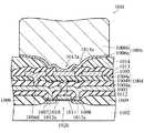
図1は、本発明の第1実施形態による半導体装置の一部の構造を示した断面図である。図2は、図1に示した第1実施形態による半導体装置の一部の構造を示した平面図である。図1および図2を参照して、本発明の第1実施形態による半導体装置1の構造について説明する。(First embodiment)
FIG. 1 is a cross-sectional view illustrating a partial structure of a semiconductor device according to a first embodiment of the present invention. FIG. 2 is a plan view showing a partial structure of the semiconductor device according to the first embodiment shown in FIG. The structure of the semiconductor device 1 according to the first embodiment of the present invention will be described with reference to FIGS.
本発明の第1実施形態による半導体装置1は、電源用ICとして用いられる。また、半導体装置1は、図1に示すように、シリコン基板2と、シリコン基板2上に形成され、半導体素子部20が形成された領域である活性領域(動作領域)を含むN型エピタキシャル層3と、N型エピタキシャル層3上に配置され、半導体素子部20と電気的に接続された1層目(最下層)の配線層4と、配線層4上に層間絶縁膜5を介して配置された2層目(最上層)の配線層6とを備えている。なお、配線層4は、本発明の「金属配線層」の一例であり、配線層6は、本発明の「金属配線層」および「最上層の金属配線層」の一例である。 The semiconductor device 1 according to the first embodiment of the present invention is used as a power supply IC. In addition, as shown in FIG. 1, the semiconductor device 1 includes an N-type epitaxial layer that includes a
シリコン基板2とN型エピタキシャル層3との界面部分の所定領域には、N+型埋め込み領域7が形成されている。また、シリコン基板2およびN型エピタキシャル層3には、半導体素子部20の両側部分に、素子分離領域8が形成されている。この素子分離領域8は、シリコン基板2とN型エピタキシャル層3との界面部分に形成されたP+型埋め込み領域8aと、N型エピタキシャル層3の表面からP+型埋め込み領域8aに接続するように形成されたP+型領域8bとを含んでいる。An N+ -type buried
また、N型エピタキシャル層3の表面部分には、ベース領域として機能するP+型領域9と、P+型領域9内に配置され、エミッタ領域として機能するN+型領域10と、P+型領域9から所定の距離を隔てて配置され、コレクタ領域として機能するN+型領域11とが形成されている。そして、P+型領域9、N+型領域10およびN+型領域11によって、NPNトランジスタからなる半導体素子部20が構成されている。The surface portion of the N-
また、N型エピタキシャル層3を覆うように、SiO2膜からなる絶縁膜12が形成されている。また、絶縁膜12上の所定領域には、アルミニウムなどからなる配線層4が形成されている。この配線層4は、1つの層により形成されていてもよいし、複数の層により形成されていてもよい。Further, an insulating
また、配線層4の一部は、絶縁膜12のスルーホール12aを介して、半導体素子部20に電気的に接続されている。 A part of the
具体的には、配線層4は、配線部4a、4b、4cおよび4dを含んでいる。この配線部4a、4bおよび4cは、絶縁膜12のスルーホール12aを介して、P+型領域9、N+型領域10およびN+型領域11にそれぞれ電気的に接続されている。Specifically, the
また、配線層4および絶縁膜12上に、層間絶縁膜5が形成されている。この層間絶縁膜5は、シリコン基板2側(下側)から順に積層されたSiN膜5aおよびポリイミド膜5bによって構成されている。 An interlayer insulating
ここで、第1実施形態では、ポリイミド膜5bは、約3μm以上の厚みを有する。また、ポリイミド膜5bは、スピン塗布法により形成されており、上面が平坦に形成されている。すなわち、ポリイミド膜5bは、配線層4に起因して発生した表面の凹凸形状を平坦化する機能を有する。 Here, in the first embodiment, the
また、ポリイミド膜5bは、半導体素子部20(活性領域)の真上の全領域に形成されている。 The
なお、ポリイミド膜5bなどの有機絶縁膜は、SiO2膜やSiN膜などの無機絶縁膜に比べて、高い弾力性を有する。このため、第1実施形態では、ポリイミド膜5bは、ワイヤーボンディングを行う際に、後述するボンディングパッド部(エリアパッド)6aに加わる荷重や圧力などが、ボンディングパッド部6aの真下の領域に位置する配線部4a、4b、4cおよび半導体素子部20に伝わるのを抑制するための緩衝材としての機能も有する。Note that the organic insulating film such as the
また、層間絶縁膜5上には、配線層6が形成されている。 A
この配線層6には、第1実施形態では、少なくとも一部が半導体素子部20(活性領域)と重なるように(半導体素子部20の真上の領域に)配置されたボンディングパッド部(エリアパッド)6aが設けられている。このボンディングパッド部6aは、全ての部分がポリイミド膜5b上に形成されている。 In the first embodiment, the
また、配線層6(ボンディングパッド部6a)は、層間絶縁膜5のスルーホール5cを介して配線層4の配線部4dに電気的に接続されている。 The wiring layer 6 (
このスルーホール5cは、図2に示すように、平面的に見て略正方形状に形成されているとともに、ボンディングパッド部6aの1つのコーナー部に位置する領域に形成されている。 As shown in FIG. 2, the through
また、図1に示すように、ボンディングパッド部6aの周辺部分、および、ポリイミド膜5bの所定領域上に、SiO2膜やSiN膜からなるカバー膜13が形成されている。Further, as shown in FIG. 1, a
また、ボンディングパッド部6a(配線層6)は、ポリイミド膜5bに接するように形成された高融点金属層6bと、高融点金属層6b上に形成されたAl層6cとによって構成されている。この高融点金属層6bは、TiWなどにより形成されており、バリアメタルとして機能する。 The
また、ボンディングパッド部6aの上面には、ワイヤーボンディングされた金線(ボンディングワイヤー)30が接続(接合)されている。 Also, a wire-bonded gold wire (bonding wire) 30 is connected (bonded) to the upper surface of the
具体的には、金線30を、ボンディングパッド部6aの上面にワイヤーボンディングする場合、ボンディングパッド部6aの上面をArガスなどを用いてプラズマ処理(プラズマクリーニング)する。これにより、ボンディングパッド部6aの上面は、清浄化される。 Specifically, when the
そして、金線30の一方側を、円筒状のキャピラリ(図示せず)を用いて、ボンディングパッド部6aの上面に1stボンディングする。このとき、ボンディングパッド部6aに、約10gf〜約200gfの荷重が加わる。 Then, one side of the
その後、金線30の他方側を、半導体装置1が搭載される支持フレーム(図示せず)などに2ndボンディングする。このようにして、金線30が、ボンディングパッド部6aの上面に接続(接合)される。 Thereafter, the other side of the
第1実施形態では、上記のように、層間絶縁膜5を、ボンディングパッド部6aの真下の領域に配置される平坦な上面を有するポリイミド膜5bを含むように構成することによって、ボンディングパッド部6aの真下の領域において、層間絶縁膜5の表面に凹凸形状が形成されるのを抑制することができる。これにより、ワイヤーボンディング時に、層間絶縁膜5にボンディングパッド部6aから荷重や圧力などが加わり亀裂が生じるのを抑制することができる。その結果、層間絶縁膜5下の金属配線層4が腐食したり断線するのを抑制することができるので、半導体素子部20とボンディングパッド部6aとを電気的に良好に接続することができる。 In the first embodiment, as described above, the
また、第1実施形態では、上記のように、ボンディングパッド部6aの真下の領域に、平坦な上面を有するポリイミド膜5bを配置することによって、ワイヤーボンディング時に、ボンディングパッド部6aに荷重や圧力などが不均一に加わるのを抑制することができる。これにより、金線30と金属配線層6(ボンディングパッド部6a)とを、電気的に良好に接続することができる。 In the first embodiment, as described above, by placing the
また、第1実施形態では、上記のように、半導体素子部20の真上の領域に、ポリイミド膜5bを配置している。ポリイミド膜5bなどの有機絶縁膜は、シリコン酸化膜やSOG膜などの無機絶縁膜に比べて弾力性が高いので、半導体素子部20の真上の領域にシリコン酸化膜やSOG膜などの無機絶縁膜を配置する場合に比べて、ワイヤーボンディング時に、ボンディングパッド部6aから半導体素子部20に荷重や圧力などが伝わるのを十分に抑制することができる。これにより、半導体素子部20にダメージが生じるのを十分に抑制することができる。 In the first embodiment, as described above, the
また、第1実施形態では、上記のように、例えばスピン塗布法などを用いてポリイミド膜5bを形成することにより、ポリイミド膜5b(層間絶縁膜5)の上面を、容易に平坦に形成することができる。 In the first embodiment, as described above, the
また、第1実施形態では、上記のように、ポリイミド膜5bと半導体素子部20との間に、SiN膜5aを形成することによって、SiN膜は機械的な強度が比較的高いので、ワイヤーボンディング時に、ボンディングパッド部6aから半導体素子部20に荷重や圧力などが伝わるのをより抑制することができる。これにより、半導体素子部20にダメージが生じるのをより十分に抑制することができる。 In the first embodiment, as described above, since the SiN film 5a is formed between the
また、第1実施形態では、上記のように、金属配線層6(ボンディングパッド部6a)を、高融点金属層6bと、高融点金属層6b上に形成されたAl層6cとを含むように構成している。これにより、TiWなどからなる高融点金属層6bは、機械的な強度が比較的高いので、ワイヤーボンディング時に、ボンディングパッド部6aから半導体素子部20に荷重や圧力などが伝わるのをより抑制することができる。これにより、半導体素子部20にダメージが生じるのをより抑制することができる。 In the first embodiment, as described above, the metal wiring layer 6 (
また、第1実施形態では、上記のように、ポリイミド膜5bを、約3μm以上の厚みに形成している。これにより、破壊強度や弾性率などの観点から、ポリイミド膜5bは、ワイヤボンディング時にボンディングパッド部6aに加えられる荷重(約10gf〜約200gf)や圧力などを十分に吸収することができる。これにより、半導体素子部20に荷重や圧力などが伝わるのを、より十分に抑制することができる。 In the first embodiment, as described above, the
また、第1実施形態では、上記のように、層間絶縁膜5のボンディングパッド部6aのコーナー部に位置する領域に、スルーホール5cを形成することによって、ワイヤーボンディング時に、円筒状のキャピラリ(図示せず)が、スルーホール5c上に当接するのを抑制することができる。これにより、スルーホール5cが損傷し、接触不良や断線が発生するのを抑制することができる。 In the first embodiment, as described above, the through-
また、第1実施形態では、上記のように、ボンディングパッド部6aをプラズマ処理(プラズマクリーニング)した後にワイヤーボンディングすることによって、荷重や圧力を低く抑えた状態で、金線30をボンディングパッド部6aに接続(接合)させることができる。これにより、半導体素子部20にダメージが生じるのをより抑制することができる。 In the first embodiment, as described above, the
また、第1実施形態では、上記のように、半導体装置1を電源用ICとして用いる。電源用ICなどの汎用デバイスは、小型化が、特に重要なので、本発明の半導体装置1を電源用ICに用いることは、特に有効である。 In the first embodiment, as described above, the semiconductor device 1 is used as a power supply IC. Since miniaturization is particularly important for general-purpose devices such as power supply ICs, it is particularly effective to use the semiconductor device 1 of the present invention for power supply ICs.
(第2実施形態)
図3は、本発明の第2実施形態による半導体装置の一部の構造を示した断面図である。図3を参照して、この第2実施形態では、上記第1実施形態とは異なり、ポリイミド膜5b上にSiN膜105cを配置した場合について説明する。(Second Embodiment)
FIG. 3 is a cross-sectional view illustrating a partial structure of the semiconductor device according to the second embodiment of the present invention. With reference to FIG. 3, in the second embodiment, unlike the first embodiment, a case where an
本発明の第2実施形態による半導体装置101では、図3に示すように、1層目(最下層)の配線層4および絶縁膜12上に、層間絶縁膜105が形成されている。この層間絶縁膜105は、シリコン基板2側(下側)から順に積層されたSiN膜5a、ポリイミド膜5bおよびSiN膜105cによって構成されている。 In the semiconductor device 101 according to the second embodiment of the present invention, as shown in FIG. 3, the
このSiN膜105cは、ポリイミド膜5bと同様、上面が平坦に形成されているとともに、半導体素子部20(活性領域)上の全域に形成されている。また、SiN膜105cは、均一の厚みに形成されている。 Similar to the
また、SiN膜105c(層間絶縁膜105)上には、2層目(最上層)の配線層6が形成されており、配線層6(ボンディングパッド部6a)は、層間絶縁膜105のスルーホール105dを介して配線層4の配線部4dに電気的に接続されている。 A second (uppermost)
なお、第2実施形態による半導体装置101のその他の構造は、上記第1実施形態と同様である。 The remaining structure of the semiconductor device 101 according to the second embodiment is similar to that of the aforementioned first embodiment.
第2実施形態では、上記のように、ボンディングパッド部6aとポリイミド膜5bとの間に、SiN膜105cを形成することによって、ワイヤーボンディング時に、ボンディングパッド部6aから半導体素子部20に荷重や圧力などが伝わるのをさらに抑制することができる。なお、ワイヤーボンディング時に、想定以上の荷重や圧力などが印加されてSiN膜105cが損傷したとしても、SiN膜105cの真下の領域に位置するポリイミド膜5bにより、ボンディングパッド部6aから半導体素子部20に荷重や圧力などが伝わるのを抑制することができるとともに、電気的絶縁性を保つことができる。すなわち、SiN膜105cが損傷しても、半導体装置101の電気的特性、品質および信頼性は劣化しない。 In the second embodiment, as described above, by forming the
なお、第2実施形態による半導体装置101のその他の効果は、上記第1実施形態と同様である。 The remaining effects of the semiconductor device 101 according to the second embodiment are similar to those of the aforementioned first embodiment.
(第3実施形態)
図4は、本発明の第3実施形態による半導体装置の一部の構造を示した断面図である。図4を参照して、この第3実施形態では、上記第1および第2実施形態とは異なり、ポリイミド膜(層間絶縁膜205)下に減圧CVD(LPCVD:Low Pressure CVD)法により形成されたLP−SiN膜212を配置した場合について説明する。(Third embodiment)
FIG. 4 is a cross-sectional view illustrating a partial structure of the semiconductor device according to the third embodiment of the present invention. Referring to FIG. 4, unlike the first and second embodiments, the third embodiment is formed under a polyimide film (interlayer insulating film 205) by a low pressure CVD (LPCVD: Low Pressure CVD) method. A case where the LP-SiN film 212 is disposed will be described.
本発明の第3実施形態による半導体装置201では、図4に示すように、SiO2膜からなる絶縁膜12上に、LP−SiN膜212が形成されている。このLP−SiN膜212は、減圧CVD法により形成されており、例えばプラズマCVD法により形成されたSiN膜に比べて、より緻密で、かつ、より機械的な強度が高い。なお、LP−SiN膜212は、本発明の「SiN膜」の一例である。In the
第3実施形態では、LP−SiN膜212は、半導体素子部20の動作に寄与しないように構成されている。 In the third embodiment, the LP-SiN film 212 is configured not to contribute to the operation of the
また、第3実施形態では、LP−SiN膜212は、活性領域(動作領域)以外の領域(ボンディングパッド部6aの真下の領域以外の領域)にも形成されており、活性領域(動作領域)以外の領域で、SiN容量として機能する。 In the third embodiment, the LP-SiN film 212 is also formed in a region other than the active region (operation region) (a region other than the region directly below the
また、LP−SiN膜212上の所定領域には、アルミニウムなどからなる配線層4が形成されている。 A
また、配線層4およびLP−SiN膜212上に、ポリイミド膜からなる層間絶縁膜205が形成されている。 An interlayer insulating film 205 made of a polyimide film is formed on the
層間絶縁膜205上には、配線層6が形成されており、配線層6(ボンディングパッド部6a)は、層間絶縁膜205のスルーホール205aを介して配線層4の配線部4dに電気的に接続されている。 A
なお、第3実施形態による半導体装置201のその他の構造は、上記第1実施形態と同様である。 The remaining structure of the
第3実施形態では、上記のように、層間絶縁膜205(ポリイミド膜)と半導体素子部20との間に、減圧CVD法を用いてLP−SiN膜212を形成している。これにより、減圧CVD法を用いて形成されたLP−SiN膜212は、例えばプラズマCVD法により形成される一般的なSiN膜に比べて、より緻密で、かつ、より機械的な強度が高いので、ワイヤーボンディング時に、ボンディングパッド部6aから半導体素子部20に荷重や圧力などが伝わるのをさらに抑制することができる。これにより、半導体素子部20にダメージが生じるのをさらに抑制することができる。また、LP−SiN膜212を、半導体素子部20の動作に寄与しないように構成することによって、ワイヤーボンディング時に、想定以上の荷重や圧力などが印加されてLP−SiN膜212が損傷したとしても、半導体装置201の電気的特性には影響しない。 In the third embodiment, as described above, the LP-SiN film 212 is formed between the interlayer insulating film 205 (polyimide film) and the
また、第3実施形態では、上記のように、LP−SiN膜212は、ボンディングパッド部6aの真下の領域以外の領域で、SiN容量として機能する。これにより、ボンディングパッド部6aの真下の領域以外の領域におけるSiN容量の形成と、半導体素子部20にダメージが生じるのを抑制するための膜(LP−SiN膜212)の形成とを同時に行うことができるので、製造プロセスを簡略化することができる。 In the third embodiment, as described above, the LP-SiN film 212 functions as a SiN capacitor in a region other than the region directly below the
なお、第3実施形態による半導体装置201のその他の効果は、上記第1実施形態と同様である。 The remaining effects of the
(第4実施形態)
図5は、本発明の第4実施形態による半導体装置の一部の構造を示した断面図である。図5を参照して、この第4実施形態では、上記第1〜第3実施形態とは異なり、半導体素子部320が抵抗体により構成されている場合について説明する。(Fourth embodiment)
FIG. 5 is a cross-sectional view illustrating a partial structure of a semiconductor device according to a fourth embodiment of the present invention. With reference to FIG. 5, unlike the said 1st-3rd embodiment, this 4th embodiment demonstrates the case where the
本発明の第4実施形態による半導体装置301では、図5に示すように、N型エピタキシャル層303の表面部分には、紙面に対して垂直方向に延びる複数のP+型領域309が形成されている。このP+型領域309とN型エピタキシャル層303との界面部分には、PN接合部が形成されている。そして、P+型領域309およびN型エピタキシャル層303によりPN接合部が形成された抵抗体によって、半導体素子部320が構成されている。なお、N型は、本発明の「第1導電型」の一例であり、P+型(P型)は、本発明の「第2導電型」の一例である。また、N型エピタキシャル層303は、本発明の「第1半導体領域」および「第3半導体領域」の一例であり、P+型領域309は、本発明の「第2半導体領域」および「第4半導体領域」の一例である。In the
第4実施形態では、P+型領域309は、イオン注入により形成されており、半導体素子部320(N型エピタキシャル層303)の上面は平坦である。In the fourth embodiment, the P+ -
また、第4実施形態では、半導体素子部320は、機械的ダメージ(ワイヤーボンディングによるダメージ)を検出する際に用いられる。具体的には、PN接合部が正常であれば逆方向に電圧を印加してもリーク電流は発生しないので、PN接合部に逆方向に電圧を印加してリーク電流が発生するか否かを検出することにより、PN接合部(半導体素子部320)に異常が発生したか否かを検出する。 In the fourth embodiment, the
また、N型エピタキシャル層303を覆うように、SiO2膜からなる絶縁膜312が形成されている。また、絶縁膜312上の所定領域には、アルミニウムなどからなる1層目(最下層)の配線層304が形成されている。なお、配線層304は、本発明の「金属配線層」の一例である。In addition, an insulating
この配線層304は、少なくとも金線30の真下の領域、および、半導体素子部320の真上の領域には形成されていない。 The
また、配線層304は、ボンディングパッド部6aの真下の領域以外の領域にも形成されており、ボンディングパッド部6aの真下の領域以外の領域で、複数のP+型領域309と電気的に接続されている。The
また、配線層304および絶縁膜312上に、層間絶縁膜305が形成されている。この層間絶縁膜305は、シリコン基板2側(下側)から順に積層されたSiN膜305aおよびポリイミド膜305bによって構成されている。 An interlayer insulating
また、第4実施形態では、配線層304が、少なくとも金線30の真下の領域、および、半導体素子部320の真上の領域には形成されていないので、少なくとも金線30の真下の領域、および、半導体素子部320の真上の領域において、SiN膜305aの上面は、平坦に形成されている。 In the fourth embodiment, since the
また、少なくとも金線30の真下の領域、および、半導体素子部320の真上の領域において、SiN膜305aおよびポリイミド膜305bは、それぞれ、均一の厚みに形成されている。 Further, the SiN film 305a and the polyimide film 305b are formed to have a uniform thickness at least in a region directly below the
なお、第4実施形態による半導体装置301のその他の構造は、上記第1実施形態と同様である。 The remaining structure of the
第4実施形態では、上記のように、半導体素子部320を、N型エピタキシャル層303と、N型エピタキシャル層303内にイオン注入により形成されたP+型領域309とにより構成される抵抗体を含むように構成している。これにより、半導体素子部320(N型エピタキシャル層303およびP+型領域309)の上面を平坦にすることができるので、半導体素子部320上に形成されるポリイミド膜305b(層間絶縁膜305)の厚みを均一にすることができる。これにより、ワイヤーボンディング時に、ボンディングパッド部6aから半導体素子部320に荷重や圧力が不均一に加わるのを抑制することができる。In the fourth embodiment, as described above, the
第4実施形態では、上記のように、機械的ダメージを検出するための半導体素子部320を設けることによって、ワイヤーボンディング時の荷重や圧力などにより、半導体装置301に異常が発生したか否かを検出することができる。これにより、異常のある半導体装置301が市場に流出するのを抑制することができる。 In the fourth embodiment, as described above, by providing the
また、第4実施形態では、上記のように、半導体素子部320を、PN接合部を有するように構成している。これにより、PN接合部が正常であれば逆方向に電圧を印加してもリーク電流は発生しないので、PN接合部に逆方向に電圧を印加してリーク電流が発生するか否かを検出することにより、PN接合部(半導体素子部320)に異常が発生したか否かを、容易に検出することができる。 In the fourth embodiment, as described above, the
なお、第4実施形態による半導体装置301のその他の効果は、上記第1実施形態と同様である。 The remaining effects of the
(第5実施形態)
図6は、本発明の第5実施形態による半導体装置の一部の構造を示した断面図である。図6を参照して、この第5実施形態では、上記第1〜第4実施形態とは異なり、半導体素子部420がESD保護素子により構成されている場合について説明する。(Fifth embodiment)
FIG. 6 is a cross-sectional view illustrating a partial structure of a semiconductor device according to a fifth embodiment of the present invention. With reference to FIG. 6, in the fifth embodiment, unlike the first to fourth embodiments, a case where the
本発明の第5実施形態による半導体装置401では、図6に示すように、1層目(最下層)の配線層404は、配線部404a、404bおよび404cを含んでいる。なお、配線層404は、本発明の「金属配線層」の一例である。 In the
第5実施形態では、配線部404aは、絶縁膜12のスルーホール12aを介して、P+型領域9およびN+型領域10に電気的に接続されている。すなわち、P+型領域9およびN+型領域10は、配線部404aを介して、互いに電気的に接続されている。In the fifth embodiment, the
また、配線部404bは、絶縁膜12のスルーホール12aを介して、N+型領域11に電気的に接続されている。また、配線部404cは、層間絶縁膜5のスルーホール5cを介して、配線層6(ボンディングパッド部6a)に電気的に接続されている。In addition, the wiring portion 404 b is electrically connected to the N+ type region 11 through the through
また、第5実施形態では、P+型領域9、N+型領域10およびN+型領域11によって、ESD保護素子として機能するファントムトランジスタからなる半導体素子部420が構成されている。In the fifth embodiment, the P+ -
また、第5実施形態では、半導体素子部420は、上記第4実施形態と同様、機械的ダメージ(ワイヤーボンディングによるダメージ)を検出する際に用いられる。 In the fifth embodiment, the
具体的には、半導体素子部420のP+型領域9とN型エピタキシャル層3との界面部分には、PN接合部が形成されている。PN接合部が正常であれば逆方向に電圧を印加してもリーク電流は発生しないので、PN接合部に逆方向に電圧を印加してリーク電流が発生するか否かを検出することにより、PN接合部(半導体素子部420)に異常が発生したか否かを検出する。Specifically, a PN junction is formed at the interface between the P+ -
なお、第5実施形態による半導体装置401のその他の構造は、上記第1実施形態と同様である。 The remaining structure of the
第5実施形態では、上記のように、機械的ダメージを検出するための半導体素子部420を、ESD保護素子により構成することによって、1つの半導体素子部420で、機械的ダメージ(ワイヤーボンディングによるダメージ)の検出と、ESD保護との両方を行うことができる。ESD保護素子は、半導体装置401の回路を保護するためにもともと設ける必要があるので、機械的ダメージを検出するための半導体素子部420を、ESD保護素子とは別に設ける場合に比べて、半導体装置401を小型化することができるとともに、製造プロセスを簡略化することができる。 In the fifth embodiment, as described above, the
なお、第5実施形態による半導体装置401のその他の効果は、上記第1および第4実施形態と同様である。 The remaining effects of the
(第6実施形態)
図7は、本発明の第6実施形態による半導体装置の一部の構造を示した断面図である。図7を参照して、この第6実施形態では、上記第4および第5実施形態とは異なり、PN接合部を用いずに、機械的ダメージを検出する場合について説明する。(Sixth embodiment)
FIG. 7 is a cross-sectional view illustrating a partial structure of a semiconductor device according to a sixth embodiment of the present invention. Referring to FIG. 7, in the sixth embodiment, unlike the fourth and fifth embodiments, a case where mechanical damage is detected without using a PN junction will be described.
本発明の第6実施形態による半導体装置501では、図7に示すように、絶縁膜12上の所定領域には、アルミニウムなどからなる1層目(最下層)の配線層504が形成されている。この配線層504は、配線部504aおよび504bを含んでいる。なお、配線層504は、本発明の「金属配線層」および「最下層の金属配線層」の一例であり、配線部504aは、本発明の「GND電位に設定された部分」の一例である。 In the
第6実施形態では、配線部504aは、GND電位に設定されている。また、配線部504bは、層間絶縁膜5のスルーホール5cを介して、2層目(最上層)の配線層6(ボンディングパッド部6a)に電気的に接続されている。 In the sixth embodiment, the
第6実施形態では、機械的ダメージ(ワイヤーボンディングによるダメージ)を検出する場合、配線層504の配線部504aと、ボンディングパッド部6aとの間の短絡を検出することにより、ワイヤーボンディング時に層間絶縁膜5にクラックなどの機械的ダメージが発生したか否かを検出する。 In the sixth embodiment, when mechanical damage (damage due to wire bonding) is detected, a short circuit between the
このとき、層間絶縁膜5にクラックなどの機械的ダメージが発生していれば、配線層504の配線部504aと、ボンディングパッド部6aとの間が短絡する。その一方、層間絶縁膜5にクラックなどの機械的ダメージが発生していなければ、配線層504の配線部504aと、ボンディングパッド部6aとの間は短絡しない。 At this time, if mechanical damage such as a crack occurs in the
また、半導体装置501には、図7とは異なる断面において、上記第1〜第5実施形態と同様、ボンディングパッド部6aの真下の領域に、トランジスタや抵抗体からなる半導体素子部(図示せず)が形成されている。 Further, in the
なお、第6実施形態による半導体装置501のその他の構造は、上記第1実施形態と同様である。 The remaining structure of the
第6実施形態では、上記のように、金属配線層504の配線部504aを、GND電位に設定し、金属配線層504の配線部504aと、ボンディングパッド部6aとの間の短絡を検出することによって、ワイヤーボンディング時に層間絶縁膜5にクラックなどの機械的ダメージが発生しているか否かを、容易に検出することができる。 In the sixth embodiment, as described above, the
なお、第6実施形態による半導体装置501のその他の効果は、上記第1実施形態と同様である。 The remaining effects of the
(第7実施形態)
図8は、本発明の第7実施形態による半導体装置の一部の構造を示した平面図である。図8を参照して、この第7実施形態では、上記第1〜第6実施形態とは異なり、層間絶縁膜605にスルーホールが4つ形成されている場合について説明する。(Seventh embodiment)
FIG. 8 is a plan view showing a partial structure of the semiconductor device according to the seventh embodiment of the present invention. With reference to FIG. 8, in the seventh embodiment, unlike the first to sixth embodiments, a case where four through holes are formed in the
本発明の第7実施形態による半導体装置601では、図8に示すように、層間絶縁膜605には、ボンディングパッド部6aの4つのコーナー部に位置する領域に、スルーホール605c、605d、605eおよび605fが形成されている。 In the
スルーホール605cは、上記第1実施形態と同様、平面的に見て略正方形状に形成されている。また、スルーホール605cは、1層目(最下層)の配線層(図示せず)と、2層目(最上層)の配線層6とを電気的に接続するように形成されている。 The through
スルーホール605d、605eおよび605fは、平面的に見てL字状に形成されている。このスルーホール605d、605eおよび605fは、1層目(最下層)の配線層(図示せず)と、2層目(最上層)の配線層6とを電気的に接続するように形成してもよいし、接続しないように形成してもよい。 The through
また、スルーホール605c、605d、605eおよび605fは、ボンディングパッド部6a(配線層6)が層間絶縁膜605から剥がれるのを抑制する機能を有する。特に、スルーホール605d、605eおよび605fは、平面的に見てL字状に形成されているので、ボンディングパッド部6a(配線層6)が層間絶縁膜605から剥がれるのを、効果的に抑制することが可能である。 The through
なお、第7実施形態による半導体装置601のその他の構造は、上記第1〜第6実施形態と同様である。 The remaining structure of the
第7実施形態では、上記のように、層間絶縁膜5のスルーホール605c、605d、605eおよび605fを、ボンディングパッド部6aの4つのコーナー部に位置する領域に形成している。これにより、ワイヤーボンディング時に、ボンディングパッド部6aに1stボンディングした後、半導体装置601が搭載される支持フレームなどに2ndボンディングする際に、金線30がキャピラリにより2ndボンディング側(支持フレーム側)に引っ張られることによりボンディングパッド部6aが層間絶縁膜605から剥がれるのを抑制することができる。 In the seventh embodiment, as described above, the through
なお、第7実施形態による半導体装置601のその他の効果は、上記第1実施形態と同様である。 The remaining effects of the
なお、今回開示された実施形態は、すべての点で例示であって制限的なものではないと考えられるべきである。本発明の範囲は、上記した実施形態の説明ではなく特許請求の範囲によって示され、さらに特許請求の範囲と均等の意味および範囲内でのすべての変更が含まれる。 The embodiment disclosed this time should be considered as illustrative in all points and not restrictive. The scope of the present invention is shown not by the above description of the embodiments but by the scope of claims for patent, and further includes all modifications within the meaning and scope equivalent to the scope of claims for patent.
たとえば、上記実施形態では、半導体装置を電源用ICとして用いる例について示したが、本発明はこれに限らず、半導体装置を電源用IC以外に用いてもよい。 For example, in the above-described embodiment, the example in which the semiconductor device is used as the power supply IC has been described. However, the present invention is not limited to this, and the semiconductor device may be used in addition to the power supply IC.
また、上記実施形態では、第1導電型をN型とし、第2導電型をP型(P+型)とする例について示したが、本発明はこれに限らず、第1導電型をP型とし、第2導電型をN型(N+型)としてもよい。In the above embodiment, an example in which the first conductivity type is the N type and the second conductivity type is the P type (P+ type) has been described. However, the present invention is not limited to this, and the first conductivity type is the P type. The second conductivity type may be an N type (N+ type).
また、上記実施形態では、ポリイミド膜からなる有機絶縁膜を用いた例について示したが、本発明はこれに限らず、ポリイミド膜以外の有機絶縁膜を用いてもよい。 Moreover, although the example using the organic insulating film made of a polyimide film has been described in the above embodiment, the present invention is not limited to this, and an organic insulating film other than the polyimide film may be used.
また、上記実施形態では、ポリイミド膜を、約3μm以上の厚みを有するように形成した例について示したが、本発明はこれに限らず、ポリイミド膜を、約3μmよりも小さい厚みを有するように形成してもよい。 In the above embodiment, the polyimide film is formed to have a thickness of about 3 μm or more. However, the present invention is not limited to this, and the polyimide film has a thickness smaller than about 3 μm. It may be formed.
また、上記実施形態では、層間絶縁膜上の配線層を、高融点金属層とAl層との2つの層により形成した例について示したが、本発明はこれに限らず、層間絶縁膜上の配線層を、1つの層(例えばAl層)により形成してもよいし、3つ以上の層により形成してもよい。 In the above embodiment, an example in which the wiring layer on the interlayer insulating film is formed of two layers of the refractory metal layer and the Al layer has been described. However, the present invention is not limited to this, and the wiring layer on the interlayer insulating film is formed. The wiring layer may be formed of one layer (for example, an Al layer) or may be formed of three or more layers.
また、上記第3実施形態では、ポリイミド膜と半導体素子部との間に、半導体素子部の動作に寄与しないLP−SiN膜を形成した例について示したが、本発明はこれに限らず、ポリイミド膜と半導体素子部との間に、半導体素子部の動作に寄与しないポリシリコン膜を形成してもよい。このように構成すれば、ポリシリコン膜は、機械的な強度が比較的高いので、ワイヤーボンディング時に、ボンディングパッド部から半導体素子部に荷重や圧力などが伝わるのを抑制することができる。また、ワイヤーボンディング時に、想定以上の荷重や圧力などが印加されてポリシリコン膜が損傷したとしても、ポリシリコン膜は半導体素子部の動作に寄与しないので、半導体装置の電気的特性には影響しない。また、このポリシリコン膜を、MOSデバイスで使用するポリシリコン膜により形成すれば、MOSデバイスの形成と、半導体素子部にダメージが生じるのを抑制するための膜(ポリシリコン膜)の形成とを同時に行うことができるので、製造プロセスを簡略化することができる。 In the third embodiment, an example is shown in which an LP-SiN film that does not contribute to the operation of the semiconductor element portion is formed between the polyimide film and the semiconductor element portion. A polysilicon film that does not contribute to the operation of the semiconductor element portion may be formed between the film and the semiconductor element portion. With such a configuration, the polysilicon film has a relatively high mechanical strength, so that it is possible to suppress transmission of a load, a pressure, and the like from the bonding pad portion to the semiconductor element portion during wire bonding. In addition, even if a load or pressure higher than expected is applied during wire bonding and the polysilicon film is damaged, the polysilicon film does not contribute to the operation of the semiconductor element portion, and thus does not affect the electrical characteristics of the semiconductor device. . If this polysilicon film is formed of a polysilicon film used in a MOS device, the formation of the MOS device and the formation of a film (polysilicon film) for suppressing damage to the semiconductor element portion are performed. Since it can be performed simultaneously, the manufacturing process can be simplified.
また、上記第7実施形態では、スルーホール605d、605eおよび605fを、平面的に見てL字状に形成した例について示したが、本発明はこれに限らず、L字状以外の形状に形成してもよい。 Further, in the seventh embodiment, the example in which the through
1、101、201、301、401、501、601 半導体装置
4、304、404 配線層(金属配線層)
5、105、205、305、605 層間絶縁膜
5a、105c、305a SiN膜
5b、305b ポリイミド膜
5c、105d、205a、605c、605d、605e、605f スルーホール
6 配線層(金属配線層、最上層の金属配線層)
6a ボンディングパッド部
6b 高融点金属層
6c Al層
20、320、420 半導体素子部
212 LP−SiN膜(SiN膜)
303 N型エピタキシャル層(第1半導体領域、第3半導体領域)
309 P+型領域(第2半導体領域、第4半導体領域)
504 配線層(金属配線層、最下層の金属配線層)
504a 配線部(GND電位に設定された部分)1, 101, 201, 301, 401, 501, 601
5, 105, 205, 305, 605
6a
303 N-type epitaxial layer (first semiconductor region, third semiconductor region)
309 P+ type region (second semiconductor region, fourth semiconductor region)
504 Wiring layer (metal wiring layer, lowermost metal wiring layer)
504a Wiring part (part set to GND potential)
Claims (18)
Translated fromJapanese複数の金属配線層と、
前記複数の金属配線層の間に配置された層間絶縁膜とを備え、
前記複数の金属配線層のうちの最上層の金属配線層は、ボンディングパッド部を含み、
前記ボンディングパッド部上には、バンプ電極が形成されておらず、
前記ボンディングパッド部は、前記層間絶縁膜を介して、前記半導体素子部と重なるように配置され、
前記層間絶縁膜は、少なくとも前記ボンディングパッド部の真下の領域、および、前記半導体素子部の真上の領域に配置される平坦な上面を有する有機絶縁膜を含むことを特徴とする半導体装置。A semiconductor element portion including at least one of a transistor and a resistor;
A plurality of metal wiring layers;
An interlayer insulating film disposed between the plurality of metal wiring layers,
The uppermost metal wiring layer of the plurality of metal wiring layers includes a bonding pad portion,
No bump electrode is formed on the bonding pad part,
The bonding pad portion is disposed so as to overlap the semiconductor element portion via the interlayer insulating film,
2. The semiconductor device according to claim 1, wherein the interlayer insulating film includes an organic insulating film having a flat upper surface disposed at least in a region directly below the bonding pad portion and a region immediately above the semiconductor element portion.
前記最上層の金属配線層と、最上層以外の前記金属配線層とは、前記スルーホールを介して電気的に接続されていることを特徴とする請求項1〜10のいずれか1項に記載の半導体装置。In the interlayer insulating film, a through hole is formed in a region located in at least one corner portion of the bonding pad portion,
11. The uppermost metal wiring layer and the metal wiring layer other than the uppermost layer are electrically connected through the through hole. Semiconductor device.
前記最下層の金属配線層のGND電位に設定された部分と、前記ボンディングパッド部との間の短絡を検出することにより、機械的ダメージが検出されることを特徴とする請求項1〜16のいずれか1項に記載の半導体装置。At least a part of the lowermost metal wiring layer among the plurality of metal wiring layers is set to the GND potential,
17. The mechanical damage is detected by detecting a short circuit between a portion set to a GND potential of the lowermost metal wiring layer and the bonding pad portion. The semiconductor device according to any one of the above.
Priority Applications (1)
| Application Number | Priority Date | Filing Date | Title |
|---|---|---|---|
| JP2008211317AJP2010050177A (en) | 2008-08-20 | 2008-08-20 | Semiconductor device |
Applications Claiming Priority (1)
| Application Number | Priority Date | Filing Date | Title |
|---|---|---|---|
| JP2008211317AJP2010050177A (en) | 2008-08-20 | 2008-08-20 | Semiconductor device |
Publications (1)
| Publication Number | Publication Date |
|---|---|
| JP2010050177Atrue JP2010050177A (en) | 2010-03-04 |
Family
ID=42067046
Family Applications (1)
| Application Number | Title | Priority Date | Filing Date |
|---|---|---|---|
| JP2008211317APendingJP2010050177A (en) | 2008-08-20 | 2008-08-20 | Semiconductor device |
Country Status (1)
| Country | Link |
|---|---|
| JP (1) | JP2010050177A (en) |
Cited By (8)
| Publication number | Priority date | Publication date | Assignee | Title |
|---|---|---|---|---|
| JPWO2012077581A1 (en)* | 2010-12-06 | 2014-05-19 | 富士電機株式会社 | Semiconductor device |
| WO2014192429A1 (en)* | 2013-05-31 | 2014-12-04 | 株式会社村田製作所 | Semiconductor device |
| JP2017085098A (en)* | 2015-10-23 | 2017-05-18 | アナログ デバイシス グローバル | Dielectric stack, isolator device, and method of forming isolator device |
| EP3264453A1 (en)* | 2016-06-27 | 2018-01-03 | Renesas Electronics Corporation | Semiconductor device |
| WO2018174191A1 (en)* | 2017-03-24 | 2018-09-27 | 株式会社村田製作所 | Capacitor |
| CN108987357A (en)* | 2017-06-05 | 2018-12-11 | 瑞萨电子株式会社 | Semiconductor device and its manufacturing method |
| JP2019212934A (en)* | 2019-09-20 | 2019-12-12 | 大日本印刷株式会社 | Display device |
| JP2020061580A (en)* | 2020-01-16 | 2020-04-16 | ルネサスエレクトロニクス株式会社 | Semiconductor device |
- 2008
- 2008-08-20JPJP2008211317Apatent/JP2010050177A/enactivePending
Cited By (17)
| Publication number | Priority date | Publication date | Assignee | Title |
|---|---|---|---|---|
| US9048278B2 (en) | 2010-12-06 | 2015-06-02 | Fuji Electric Co., Ltd. | Semiconductor device |
| JPWO2012077581A1 (en)* | 2010-12-06 | 2014-05-19 | 富士電機株式会社 | Semiconductor device |
| WO2014192429A1 (en)* | 2013-05-31 | 2014-12-04 | 株式会社村田製作所 | Semiconductor device |
| JP2017085098A (en)* | 2015-10-23 | 2017-05-18 | アナログ デバイシス グローバル | Dielectric stack, isolator device, and method of forming isolator device |
| EP3264453A1 (en)* | 2016-06-27 | 2018-01-03 | Renesas Electronics Corporation | Semiconductor device |
| JP2018006385A (en)* | 2016-06-27 | 2018-01-11 | ルネサスエレクトロニクス株式会社 | Semiconductor device |
| US10204853B2 (en) | 2016-06-27 | 2019-02-12 | Renesas Electronics Corporation | Semiconductor device |
| US10879347B2 (en) | 2017-03-24 | 2020-12-29 | Murata Manufacturing Co., Ltd. | Capacitor |
| WO2018174191A1 (en)* | 2017-03-24 | 2018-09-27 | 株式会社村田製作所 | Capacitor |
| CN110326073B (en)* | 2017-03-24 | 2021-09-21 | 株式会社村田制作所 | Capacitor with a capacitor element |
| CN110326073A (en)* | 2017-03-24 | 2019-10-11 | 株式会社村田制作所 | Capacitor |
| JPWO2018174191A1 (en)* | 2017-03-24 | 2019-11-07 | 株式会社村田製作所 | Capacitors |
| JP2018206938A (en)* | 2017-06-05 | 2018-12-27 | ルネサスエレクトロニクス株式会社 | Semiconductor device and manufacturing method of the same |
| CN108987357A (en)* | 2017-06-05 | 2018-12-11 | 瑞萨电子株式会社 | Semiconductor device and its manufacturing method |
| CN108987357B (en)* | 2017-06-05 | 2023-10-31 | 瑞萨电子株式会社 | Semiconductor device and manufacturing method thereof |
| JP2019212934A (en)* | 2019-09-20 | 2019-12-12 | 大日本印刷株式会社 | Display device |
| JP2020061580A (en)* | 2020-01-16 | 2020-04-16 | ルネサスエレクトロニクス株式会社 | Semiconductor device |
Similar Documents
| Publication | Publication Date | Title |
|---|---|---|
| JP2010050177A (en) | Semiconductor device | |
| US7629689B2 (en) | Semiconductor integrated circuit having connection pads over active elements | |
| US10497662B2 (en) | Semiconductor device and ball bonder | |
| TW201351585A (en) | Semiconductor device and manufacturing method for the same | |
| JP5570727B2 (en) | Semiconductor device | |
| US7301229B2 (en) | Electrostatic discharge (ESD) protection for integrated circuit packages | |
| JP5301231B2 (en) | Semiconductor device | |
| JP3898350B2 (en) | Semiconductor device | |
| JP2006332533A (en) | Semiconductor device and manufacturing method thereof | |
| JP4938983B2 (en) | Semiconductor integrated circuit | |
| JP4165460B2 (en) | Semiconductor device | |
| US7898035B2 (en) | Semiconductor device | |
| US20060043605A1 (en) | Semiconductor device | |
| JP2008078354A (en) | Semiconductor device | |
| JP2009176833A (en) | Semiconductor device and manufacturing method thereof | |
| JP2007059867A (en) | Semiconductor device | |
| JP3608393B2 (en) | Semiconductor device | |
| JP4093165B2 (en) | Semiconductor integrated circuit device | |
| JP4682622B2 (en) | Semiconductor device | |
| US20090026562A1 (en) | Package structure for optoelectronic device | |
| JP4221019B2 (en) | Semiconductor device | |
| WO2021187187A1 (en) | Semiconductor device, method for manufacturing semiconductor device, and electronic apparatus | |
| CN100590858C (en) | Semiconductor device | |
| JP2006318989A (en) | Semiconductor device | |
| KR100971211B1 (en) | Semiconductor chip package and its manufacturing method for crack prevention |