JP2010041720A - Pixel array of three-dimensional image sensor - Google Patents
Pixel array of three-dimensional image sensorDownload PDFInfo
- Publication number
- JP2010041720A JP2010041720AJP2009176470AJP2009176470AJP2010041720AJP 2010041720 AJP2010041720 AJP 2010041720AJP 2009176470 AJP2009176470 AJP 2009176470AJP 2009176470 AJP2009176470 AJP 2009176470AJP 2010041720 AJP2010041720 AJP 2010041720A
- Authority
- JP
- Japan
- Prior art keywords
- pixel
- pixels
- color
- image sensor
- distance measurement
- Prior art date
- Legal status (The legal status is an assumption and is not a legal conclusion. Google has not performed a legal analysis and makes no representation as to the accuracy of the status listed.)
- Pending
Links
Images


Classifications
- H—ELECTRICITY
- H10—SEMICONDUCTOR DEVICES; ELECTRIC SOLID-STATE DEVICES NOT OTHERWISE PROVIDED FOR
- H10F—INORGANIC SEMICONDUCTOR DEVICES SENSITIVE TO INFRARED RADIATION, LIGHT, ELECTROMAGNETIC RADIATION OF SHORTER WAVELENGTH OR CORPUSCULAR RADIATION
- H10F39/00—Integrated devices, or assemblies of multiple devices, comprising at least one element covered by group H10F30/00, e.g. radiation detectors comprising photodiode arrays
- H10F39/10—Integrated devices
- H10F39/12—Image sensors
- H10F39/18—Complementary metal-oxide-semiconductor [CMOS] image sensors; Photodiode array image sensors
- H10F39/182—Colour image sensors
- H—ELECTRICITY
- H04—ELECTRIC COMMUNICATION TECHNIQUE
- H04N—PICTORIAL COMMUNICATION, e.g. TELEVISION
- H04N13/00—Stereoscopic video systems; Multi-view video systems; Details thereof
- H04N13/20—Image signal generators
- H04N13/204—Image signal generators using stereoscopic image cameras
- H04N13/207—Image signal generators using stereoscopic image cameras using a single 2D image sensor
- H04N13/229—Image signal generators using stereoscopic image cameras using a single 2D image sensor using lenticular lenses, e.g. arrangements of cylindrical lenses
- H—ELECTRICITY
- H04—ELECTRIC COMMUNICATION TECHNIQUE
- H04N—PICTORIAL COMMUNICATION, e.g. TELEVISION
- H04N13/00—Stereoscopic video systems; Multi-view video systems; Details thereof
- H04N13/20—Image signal generators
- H04N13/257—Colour aspects
- H—ELECTRICITY
- H04—ELECTRIC COMMUNICATION TECHNIQUE
- H04N—PICTORIAL COMMUNICATION, e.g. TELEVISION
- H04N23/00—Cameras or camera modules comprising electronic image sensors; Control thereof
- H04N23/10—Cameras or camera modules comprising electronic image sensors; Control thereof for generating image signals from different wavelengths
- H04N23/11—Cameras or camera modules comprising electronic image sensors; Control thereof for generating image signals from different wavelengths for generating image signals from visible and infrared light wavelengths
- H—ELECTRICITY
- H04—ELECTRIC COMMUNICATION TECHNIQUE
- H04N—PICTORIAL COMMUNICATION, e.g. TELEVISION
- H04N25/00—Circuitry of solid-state image sensors [SSIS]; Control thereof
- H04N25/10—Circuitry of solid-state image sensors [SSIS]; Control thereof for transforming different wavelengths into image signals
- H04N25/11—Arrangement of colour filter arrays [CFA]; Filter mosaics
- H04N25/13—Arrangement of colour filter arrays [CFA]; Filter mosaics characterised by the spectral characteristics of the filter elements
- H04N25/131—Arrangement of colour filter arrays [CFA]; Filter mosaics characterised by the spectral characteristics of the filter elements including elements passing infrared wavelengths
- H—ELECTRICITY
- H04—ELECTRIC COMMUNICATION TECHNIQUE
- H04N—PICTORIAL COMMUNICATION, e.g. TELEVISION
- H04N25/00—Circuitry of solid-state image sensors [SSIS]; Control thereof
- H04N25/10—Circuitry of solid-state image sensors [SSIS]; Control thereof for transforming different wavelengths into image signals
- H04N25/11—Arrangement of colour filter arrays [CFA]; Filter mosaics
- H04N25/13—Arrangement of colour filter arrays [CFA]; Filter mosaics characterised by the spectral characteristics of the filter elements
- H04N25/135—Arrangement of colour filter arrays [CFA]; Filter mosaics characterised by the spectral characteristics of the filter elements based on four or more different wavelength filter elements
- H—ELECTRICITY
- H04—ELECTRIC COMMUNICATION TECHNIQUE
- H04N—PICTORIAL COMMUNICATION, e.g. TELEVISION
- H04N25/00—Circuitry of solid-state image sensors [SSIS]; Control thereof
- H04N25/70—SSIS architectures; Circuits associated therewith
- H04N25/703—SSIS architectures incorporating pixels for producing signals other than image signals
- H04N25/705—Pixels for depth measurement, e.g. RGBZ
- H—ELECTRICITY
- H04—ELECTRIC COMMUNICATION TECHNIQUE
- H04N—PICTORIAL COMMUNICATION, e.g. TELEVISION
- H04N25/00—Circuitry of solid-state image sensors [SSIS]; Control thereof
- H04N25/70—SSIS architectures; Circuits associated therewith
- H04N25/76—Addressed sensors, e.g. MOS or CMOS sensors
- H04N25/77—Pixel circuitry, e.g. memories, A/D converters, pixel amplifiers, shared circuits or shared components
- H04N25/778—Pixel circuitry, e.g. memories, A/D converters, pixel amplifiers, shared circuits or shared components comprising amplifiers shared between a plurality of pixels, i.e. at least one part of the amplifier must be on the sensor array itself
- H—ELECTRICITY
- H10—SEMICONDUCTOR DEVICES; ELECTRIC SOLID-STATE DEVICES NOT OTHERWISE PROVIDED FOR
- H10F—INORGANIC SEMICONDUCTOR DEVICES SENSITIVE TO INFRARED RADIATION, LIGHT, ELECTROMAGNETIC RADIATION OF SHORTER WAVELENGTH OR CORPUSCULAR RADIATION
- H10F39/00—Integrated devices, or assemblies of multiple devices, comprising at least one element covered by group H10F30/00, e.g. radiation detectors comprising photodiode arrays
- H10F39/80—Constructional details of image sensors
- H10F39/813—Electronic components shared by multiple pixels, e.g. one amplifier shared by two pixels
Landscapes
- Engineering & Computer Science (AREA)
- Multimedia (AREA)
- Signal Processing (AREA)
- Physics & Mathematics (AREA)
- Spectroscopy & Molecular Physics (AREA)
- Solid State Image Pick-Up Elements (AREA)
- Transforming Light Signals Into Electric Signals (AREA)
- Color Television Image Signal Generators (AREA)
- Measurement Of Optical Distance (AREA)
Abstract
Translated fromJapaneseDescription
Translated fromJapanese本発明は、立体カラーイメージセンサのピクセルアレイに係り、特に、隣接するように配置された複数の距離測定ピクセルを、選択的にそれぞれ、または統合して距離を測定する立体イメージセンサに関する。 The present invention relates to a pixel array of a stereoscopic color image sensor, and more particularly to a stereoscopic image sensor that measures a distance by selectively or integrating a plurality of distance measuring pixels arranged adjacent to each other.
立体イメージセンサは、物体のカラーイメージと物体との距離とを測定し、立体的に物体のカラーを再現するセンサである。立体イメージセンサは、カラー測定用ピクセルと距離測定ピクセルとを具備する。カラー測定用ピクセル(「カラーピクセル」とも称する)は、レッドピクセル、グリーンピクセル及びブルーピクセルを具備し、それらカラーピクセルと距離測定ピクセルは、アレイ状に配列される。 A three-dimensional image sensor is a sensor that measures the color image of an object and the distance between the object and reproduces the color of the object three-dimensionally. The stereoscopic image sensor includes a color measurement pixel and a distance measurement pixel. Color measurement pixels (also referred to as “color pixels”) include red pixels, green pixels, and blue pixels, and the color pixels and distance measurement pixels are arranged in an array.
カラーピクセルは、小サイズ、例えば、2ミクロン以下のサイズに形成されうるが、一般的な距離測定ピクセルは、カラーピクセルより大きく形成される。これによって、カラーピクセルでのマイクロレンズと距離測定ピクセルで使われるマイクロレンズとのサイズが変わり、また、光電変換素子、例えば、フォトダイオードの基板での位置が異なることになるために、製造工程上、立体イメージセンサを製造し難いという点がある。 Color pixels can be formed in small sizes, eg, 2 microns or less, while typical distance measurement pixels are formed larger than color pixels. This changes the size of the microlens in the color pixel and the microlens used in the distance measurement pixel, and also changes the position of the photoelectric conversion element, for example, the photodiode on the substrate. However, it is difficult to manufacture a stereoscopic image sensor.
一方、一般的な従来の立体イメージセンサは、照度によって感度(sensitivity)が低くありうる。 Meanwhile, a general conventional stereoscopic image sensor may have low sensitivity depending on illuminance.
特許文献1には、ダイナミックレンジ(dynamic range)の拡大のために、1つのカラーフィルタに4個のピクセルを配し、1つの単位ピクセルとして使用する構成が開示されている。
本発明は、照度によって距離測定ピクセルの領域を変更できる立体イメージセンサのピクセルアレイを提供する。 The present invention provides a pixel array of a stereoscopic image sensor that can change a region of a distance measurement pixel according to illuminance.
本発明は、ピクセルアレイ上に形成されたマイクロレンズのサイズが同一であって、光電変換部の位置が同一である立体イメージセンサを提供する。 The present invention provides a stereoscopic image sensor in which the size of microlenses formed on a pixel array is the same and the position of a photoelectric conversion unit is the same.
本発明の一実施形態による立体イメージセンサのピクセルアレイは、カラーピクセルと距離測定ピクセルとを含む単位ピクセル・パターンがアレイ状に配列されており、前記単位ピクセル・パターンは、隣接する前記単位ピクセル・パターンと前記距離測定ピクセルとが互いに隣接するように配される。 A pixel array of a stereoscopic image sensor according to an embodiment of the present invention has unit pixel patterns including color pixels and distance measurement pixels arranged in an array, and the unit pixel pattern includes adjacent unit pixel patterns. A pattern and the distance measuring pixel are arranged adjacent to each other.
前記隣接するように配された前記距離測定ピクセルは4個であり、前記4個の距離測定ピクセルは、正方形状に配されうる。 The distance measuring pixels arranged adjacent to each other may be four, and the four distance measuring pixels may be arranged in a square shape.
前記カラーピクセルは、レッドピクセル(R),グリーンピクセル(G),ブルーピクセル(B),マゼンタピクセル(Mg),シアンピクセル(Cy),イエローピクセル(Y),ホワイトピクセル(W)のうち、選択された少なくとも2つのピクセルを含む。 The color pixel is selected from a red pixel (R), a green pixel (G), a blue pixel (B), a magenta pixel (Mg), a cyan pixel (Cy), a yellow pixel (Y), and a white pixel (W). At least two pixels.
前記カラーピクセルと前記距離測定ピクセルは、実質的に同一サイズに形成される。 The color pixel and the distance measuring pixel are formed to have substantially the same size.
本発明の他の実施形態による立体イメージセンサのピクセルアレイは、隣接したN個の第1カラーピクセルを含む第1カラーピクセル・パターンと、隣接したN個の第2カラーピクセルを含む第2カラーピクセル・パターンと、隣接したN個の第3カラーピクセルを含む第3カラーピクセル・パターンと、距離測定ピクセル・パターンとを含み、前記Nは、2より大きい自然数である。 A pixel array of a stereoscopic image sensor according to another embodiment of the present invention includes a first color pixel pattern including N adjacent first color pixels and a second color pixel including adjacent N second color pixels. A pattern, a third color pixel pattern including N adjacent third color pixels, and a distance measuring pixel pattern, wherein N is a natural number greater than two.
前記第1カラーピクセルないし第3カラーピクセルは、レッドピクセル(R),グリーンピクセル(G),ブルーピクセル(B),マゼンタピクセル(Mg),シアンピクセル(Cy),イエローピクセル(Y),ホワイトピクセル(W)のうち、選択されたピクセルである。 The first to third color pixels are a red pixel (R), a green pixel (G), a blue pixel (B), a magenta pixel (Mg), a cyan pixel (Cy), a yellow pixel (Y), and a white pixel. It is the selected pixel in (W).
本発明の一局面によれば、前記距離測定用ピクセル・パターンは、隣接したN個の距離測定ピクセルを具備し、前記カラーピクセルと前記距離測定ピクセルは、実質的に同じサイズに形成されうる。 According to an aspect of the present invention, the distance measurement pixel pattern may include N distance measurement pixels adjacent to each other, and the color pixel and the distance measurement pixel may be formed to have substantially the same size.
本発明の他の局面によれば、前記距離測定用ピクセルは、前記カラーピクセルのN倍のサイズに形成される。 According to another aspect of the present invention, the distance measuring pixel is formed to be N times as large as the color pixel.
本発明のまた他の実施形態による立体イメージセンサのピクセルアレイは、複数の隣接したカラーピクセルを含むカラーピクセル・パターンと、前記カラーピクセル・パターンと実質的に同じサイズを有する距離測定ピクセル・パターンとを具備する。 A pixel array of a stereoscopic image sensor according to another embodiment of the present invention includes a color pixel pattern including a plurality of adjacent color pixels, and a distance measurement pixel pattern having substantially the same size as the color pixel pattern. It comprises.
本発明の一局面によれば、前記距離測定ピクセル・パターンは、複数の距離測定ピクセルを具備する。 According to one aspect of the invention, the distance measuring pixel pattern comprises a plurality of distance measuring pixels.
本発明の他の局面によれば、前記距離測定ピクセル・パターンは、前記カラーピクセル・パターンと実質的に同じサイズを有する距離測定ピクセルを具備する。 According to another aspect of the invention, the distance measuring pixel pattern comprises distance measuring pixels having substantially the same size as the color pixel pattern.
本発明の実施形態による立体イメージセンサは、カラーピクセルと距離測定ピクセルとを含む単位ピクセル・パターンがアレイ状に配列されており、前記単位ピクセル・パターンは、隣接する前記単位ピクセル・パターンと前記距離測定用ピクセルとが互いに隣接するように配されたピクセルアレイと、前記各ピクセルに対応するように形成されたマイクロレンズとを具備し、前記マイクロレンズは、実質的に同じサイズに形成される。 In the stereoscopic image sensor according to the embodiment of the present invention, unit pixel patterns including color pixels and distance measurement pixels are arranged in an array, and the unit pixel pattern includes the adjacent unit pixel pattern and the distance. A pixel array including measurement pixels arranged adjacent to each other and a microlens formed to correspond to each pixel are provided, and the microlenses are formed to have substantially the same size.
本発明の実施形態による立体イメージセンサのピクセルアレイは、複数の距離測定ピクセルが互いに隣接するように配され、照度によって、それぞれまたは統合して距離を測定できるので、必要によってイメージ解像度または感度を向上させることができる。 The pixel array of the stereoscopic image sensor according to the embodiment of the present invention is arranged such that a plurality of distance measurement pixels are adjacent to each other, and the distance can be measured by illuminance individually or in combination, so that the image resolution or sensitivity is improved as necessary. Can be made.
また、同じマイクロレンズと基板とに同じ深さに形成された光電変換素子を具備するので、その製造工程が容易である。 Moreover, since the photoelectric conversion element formed in the same depth on the same microlens and a board | substrate is comprised, the manufacturing process is easy.
以下、添付された図面を参照しつつ、本発明の望ましい実施形態による立体イメージセンサのピクセルアレイについて詳細に説明する。 Hereinafter, a pixel array of a stereoscopic image sensor according to an exemplary embodiment of the present invention will be described in detail with reference to the accompanying drawings.
図1は、本発明の一実施形態による立体イメージセンサのピクセルアレイ100を概略的に示す平面図である。 FIG. 1 is a plan view schematically illustrating a
図1を参照すれば、立体イメージセンサのピクセルアレイ100は、カラーピクセルであるレッドピクセル(R),グリーンピクセル(G),ブルーピクセル(B)と、距離測定ピクセル(Z)とを具備する。該ピクセル(R,G,B,Z)は、1つの四角形状をなしつつ、アレイ状に配列される。各ピクセルは、実質的に同じサイズに形成されうる。 Referring to FIG. 1, a
互いに隣接するように配された複数、例えば、4個の単位ピクセル・パターン102の4個の距離測定ピクセル(Z)は、互いに隣接して配され、四角形状をなすように配されている。距離測定ピクセル(Z)は、赤外線波長を有した光度を測定し、他のカラーピクセルの波長の光と比較して照度が低い場合、光の検出感度が低い。 A plurality of, for example, four distance measurement pixels (Z) of the four
カラーピクセルは、図1では、レッドピクセル(R),グリーンピクセル(G),ブルーピクセル(B)を含むが、必ずしもそれらに限定されるものではない。例えば、レッドピクセル(R),グリーンピクセル(G),ブルーピクセル(B),マゼンタピクセル(Mg),シアンピクセル(Cy),イエローピクセル(Y),ホワイトピクセル(W)のうち、少なくとも2つのピクセルを含んでなされうる。 In FIG. 1, the color pixels include a red pixel (R), a green pixel (G), and a blue pixel (B), but are not necessarily limited thereto. For example, at least two of a red pixel (R), a green pixel (G), a blue pixel (B), a magenta pixel (Mg), a cyan pixel (Cy), a yellow pixel (Y), and a white pixel (W). Can be made.
図2は、図1のII−II線に沿って切り取った断面図である。図2を参照すれば、基板120、例えば、p型シリコン基板に、グリーンピクセル(G),レッドピクセル(R)と、距離測定ピクセル(Z)とが形成されている。グリーンピクセル(G)は、マイクロレンズ130とグリーンフィルタ131と光電変換素子132とを具備する。レッドピクセル(R)は、マイクロレンズ140とレッドフィルタ141と光電変換素子142とを具備する。光電変換素子132,142はn型領域であって、p型基板120と共に、p−n接合フォトダイオードを形成できる。 2 is a cross-sectional view taken along line II-II in FIG. Referring to FIG. 2, a green pixel (G), a red pixel (R), and a distance measuring pixel (Z) are formed on a
距離測定ピクセル(Z)は、マイクロレンズ150と赤外線フィルタ151と光電変換素子152とを具備する。光電変換素子152はn型領域であって、p型基板と共に、p−n接合フォトダイオードを形成できる。 The distance measurement pixel (Z) includes a
光電変換素子132,142,152は、以下では、フォトダイオードとも称することも可能である。また、カラーフィルタは、レッドフィルタ、グリーンフィルタ、ブルーフィルタだけではなく、赤外線フィルタを指すことも可能である。 The
マイクロレンズ130,140,150は、実質的に同じサイズに形成されうる。光電変換素子132,142,152は、マイクロレンズ130,140,150から集束された光を受け、マイクロレンズ130,140,150が実質的に同じサイズに形成されるので、光電変換素子132,142,152は、基板120の表面から実質的に同じ深さに形成されうる。また、図2には図示されていないが、ブルーピクセル(B)も、グリーンピクセル(G),レッドピクセル(R)及び距離測定ピクセル(Z)と実質的にその構造が同一でありうる。 The
従って、本発明の実施形態によるイメージセンサは、従来の半導体工程を使用して容易に、基板120で同じ位置に光電変換素子を形成し、エッチングによって同じサイズのマイクロレンズを製造するので、その製造工程が容易でありうる。 Therefore, the image sensor according to the embodiment of the present invention can easily form microlenses having the same size by forming photoelectric conversion elements at the same position on the
図3は、本発明の他の実施形態による立体イメージセンサのピクセルアレイ200を概略的に示す平面図である。 FIG. 3 is a plan view schematically illustrating a
図3を参照すれば、ピクセルアレイ200は、レッドピクセル・パターン202,グリーンピクセル・パターン204,ブルーピクセル・パターン206からなるカラーピクセル・パターンと、距離測定ピクセル・パターン208とを具備する。各ピクセル・パターン202,204,206と距離測定ピクセル・パターン208は、実質的に同じサイズに形成されうる。 Referring to FIG. 3, the
レッドピクセル・パターン202,グリーンピクセル・パターン204,ブルーピクセル・パターン206は、それぞれ4個のレッドピクセル(R)、4個のグリーンピクセル(G)及び4個のブルーピクセル(B)を含む。図3には、各カラーピクセル・パターンが4個のカラーピクセルを具備したところを図示しているが、必ずしもこれに限定されるものではない。例えば、各カラーピクセル・パターンは、複数個、例えば、2,3個によって形成されうる。 Each of the
カラーピクセル・パターンは、図3では、レッドピクセル(R),グリーンピクセル(G),ブルーピクセル(B)を含むが、必ずしもこれに限定されるものではない。例えば、レッドピクセル(R),グリーンピクセル(G),ブルーピクセル(B),マゼンタピクセル(Mg),シアンピクセル(Cy),イエローピクセル(Y),ホワイトピクセル(W)のうち、少なくとも3個のピクセルを含んでなされうる。 In FIG. 3, the color pixel pattern includes a red pixel (R), a green pixel (G), and a blue pixel (B), but is not necessarily limited thereto. For example, at least three of a red pixel (R), a green pixel (G), a blue pixel (B), a magenta pixel (Mg), a cyan pixel (Cy), a yellow pixel (Y), and a white pixel (W). It can be done including pixels.
距離測定ピクセル・パターン208は複数個、例えば、4個の距離測定ピクセル(Z)を含む。それら4個の距離測定ピクセル(Z)は、互いに隣接するように配されている。距離測定ピクセル(Z)は赤外線波長を有した光度を測定し、他のカラーピクセルの波長の光と比較して照度が低い場合、光の検出感度が低い。 The distance
各カラーピクセルR,G,Bも、4個の同種のピクセルが互いに隣接するように配されている。 Each color pixel R, G, B is also arranged so that four pixels of the same kind are adjacent to each other.
図4は、図3のIV−IV線に沿って切り取った断面図である。図4を参照すれば、基板220、例えば、p型シリコン基板上にレッドピクセル(R)と距離測定ピクセル(Z)とが形成されている。レッドピクセル(R)は、マイクロレンズ230とレッドフィルタ231と光電変換素子232とを具備する。光電変換素子232はn型領域であって、p型基板220と共に、p−n接合フォトダイオードを形成できる。 4 is a cross-sectional view taken along line IV-IV in FIG. Referring to FIG. 4, a red pixel (R) and a distance measuring pixel (Z) are formed on a
距離測定ピクセル(Z)は、マイクロレンズ240と赤外線フィルタ241と光電変換素子242とを具備する。光電変換素子242はn型領域であって、p型基板と共に、p−n接合フォトダイオードを形成できる。光電変換素子は、以下では、フォトダイオードとも称することも可能である。また、カラーフィルタは、レッドフィルタ、グリーンフィルタ、ブルーフィルタだけではなく、赤外線フィルタを指すこともできる。 The distance measurement pixel (Z) includes a
マイクロレンズ230,240は、実質的に同じサイズに形成されうる。光電変換素子232,242は、マイクロレンズ230,240から集束された光を受け、マイクロレンズ230,240が実質的に同じサイズに形成されるので、光電変換素子232,242は、基板220の表面から実質的に同じ深さに形成されうる。また、図4には図示されていないが、グリーンピクセル(G)及びブルーピクセル(B)も、レッドピクセル(R)及び距離測定ピクセル(Z)と実質的にその構造が同一でありうる。 The
従って、本発明の他の実施形態によるイメージセンサは、従来の半導体工程を使用して容易に、基板220で同じ位置に光電変換素子を形成し、エッチングによって同じサイズのマイクロレンズを製造するので、その製造工程が容易でありうる。 Accordingly, an image sensor according to another embodiment of the present invention easily forms a photoelectric conversion element at the same position on the
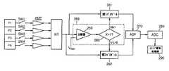
図5は、本発明のさらに他の実施形態による立体イメージセンサの構成を示すブロック図の一例である。 FIG. 5 is an example of a block diagram showing a configuration of a stereoscopic image sensor according to still another embodiment of the present invention.
図5を参照すれば、図4でのように、隣接した4個の同じカラーピクセルP1〜P4と、それぞれのピクセルP1〜P4と連結された4個の増幅器AMPと、前記4個の増幅器AMPからの電気的信号が入力される統合器INTとを具備する。各ピクセルP1〜P4と各増幅器AMPとの間には、スイッチング素子SW1〜SW4が設けられる。 Referring to FIG. 5, as in FIG. 4, four adjacent color pixels P1 to P4, four amplifiers AMP connected to the respective pixels P1 to P4, and the four amplifiers AMP. And an integrator INT to which an electrical signal from is input. Switching elements SW1 to SW4 are provided between the pixels P1 to P4 and the amplifiers AMP.
カラーピクセルP1〜P4は、レッドピクセル(R),グリーンピクセル(G),ブルーピクセル(B),マゼンタピクセル(Mg),シアンピクセル(Cy),イエローピクセル(Y),ホワイトピクセル(W)のうち、一つでありうる。 The color pixels P1 to P4 are red pixels (R), green pixels (G), blue pixels (B), magenta pixels (Mg), cyan pixels (Cy), yellow pixels (Y), and white pixels (W). Can be one.
スイッチング素子SW1〜SW4がいずれもターンオンされれば、ピクセルP1〜P4からの信号は統合器INTに統合され、統合器INTからの信号は、比較器250及び判断器260に入力される。比較器250は、入力された信号を基準値VHighと比較し、前記基準値VHigh以下であるならば、判断器260に「1」信号を出力し、そうでなければ、「0」信号を出力する。これによって判断器260は、前記信号が「1」であるならば、第1パスゲート261をオープンし、「0」であるならば、第2パスゲート262をオープンする。第1パスゲート261には、統合器INTからの統合されたアナログ信号が入力され、該信号は、アナログシグナル処理部(ASP)270に入力される。When all of the switching elements SW1 to SW4 are turned on, the signals from the pixels P1 to P4 are integrated into the integrator INT, and the signals from the integrator INT are input to the
第2パスゲート262がオープンされる場合、第1スイッチング素子SW1〜第4スイッチング素子SW4は、順次に開閉され、第1ピクセルP1〜第4ピクセルP4からの電気信号は、統合器INTに順次に入力され、従って、それらの信号は、アナログシグナル処理部(ASP)270に順次に入力される。 When the
比較器250及び判断器260は信号制御部269を形成し、照度によって、アナログシグナル処理部(ASP)270に入力される信号を選択する。 The
アナログシグナル処理部(ASP)270に入力された信号は、アナログ・デジタルコンバータ(ADC)280に入ってデジタル信号に変わり、次に、イメージ信号処理部290に入力される。 The signal input to the analog signal processing unit (ASP) 270 enters the analog / digital converter (ADC) 280 to be converted into a digital signal, and is then input to the image
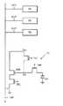
図6は、図5のピクセルの等価回路図である。 FIG. 6 is an equivalent circuit diagram of the pixel of FIG.
図6を参照すれば、各ピクセルP1〜P4は、トランスファトランジスタTRF、リセットトランジスタRST、ドライブトランジスタDRV、選択トランジスタSELを具備する。第1ピクセルP1〜第4ピクセルP4の出力ライン(選択トランジスタSELの一端に連結された出力ラインOUT)は、統合出力ライン291に並列に連結される。 Referring to FIG. 6, each of the pixels P1 to P4 includes a transfer transistor TRF, a reset transistor RST, a drive transistor DRV, and a selection transistor SEL. The output lines of the first pixel P1 to the fourth pixel P4 (the output line OUT connected to one end of the selection transistor SEL) are connected in parallel to the
フローティング拡散領域FDは、ドライブトランジスタDRVのゲート及びリセットトランジスタRSTに連結され、ドライブトランジスタDRVは、選択トランジスタSELを介して統合出力ライン291に、フローティング拡散領域FDからの信号を出力する。 The floating diffusion region FD is connected to the gate of the drive transistor DRV and the reset transistor RST, and the drive transistor DRV outputs a signal from the floating diffusion region FD to the
図5の第1スイッチSW1〜第4スイッチSW4は、第1選択トランジスタSEL〜第4選択トランジスタSELでありうる。また、第1スイッチSW1〜第4スイッチSW4は、第1選択トランジスタSEL〜第4選択トランジスタSELと統合出力ライン291との間にそれぞれ形成されたスイッチ(図示せず)でありうる。 The first switch SW1 to the fourth switch SW4 in FIG. 5 may be a first selection transistor SEL to a fourth selection transistor SEL. Further, the first switch SW1 to the fourth switch SW4 may be switches (not shown) formed between the first selection transistor SEL to the fourth selection transistor SEL and the
図5の統合器INTは、統合出力ライン291であって、第1ピクセルP1〜第4ピクセルP4からの信号がいずれも統合されるためには、第1スイッチSW1〜第4スイッチSW4をいずれも同時にターンオンさせねばならない。そして、各ピクセルP1〜P4からの信号をそれぞれ得るためには、第1スイッチSW1〜第4スイッチSW4を順次にターンオンさせる。 The integrator INT of FIG. 5 is an
図5の各増幅器AMPは、当該ピクセルのドライブトランジスタDRVと選択トランジスタSELとによって構成されうる。 Each amplifier AMP in FIG. 5 can be constituted by a drive transistor DRV and a selection transistor SEL of the pixel.
図5及び図6によるピクセル構造では、アナログシグナル処理部(ASP)270に入力される信号が1つの信号であるから、アナログ・デジタルコンバータ(ADC)280の数が減ることが可能である。 In the pixel structure according to FIGS. 5 and 6, since the signal input to the analog signal processing unit (ASP) 270 is one signal, the number of analog-to-digital converters (ADC) 280 can be reduced.
本発明の一実施形態に立体イメージセンサ200は、照度が低いときは、4個のピクセル領域に照射された光の和で1つのピクセルデータを算出し、各ピクセルのデータとして使用でき、従って、感度を向上させることができる。また、照度が高い場合には、各ピクセルを独立的に使用してイメージデータとして使用するので、イメージ解像度を上昇させることができる。 When the illuminance is low, the
図7は、図1及び図3に図示された距離測定ピクセルの等価回路図である。前記実施形態の構成要素と実質的に同じ構成要素には、同じ参照番号を使用して詳細な説明は省略する。 FIG. 7 is an equivalent circuit diagram of the distance measurement pixel illustrated in FIGS. 1 and 3. The same reference numerals are used for substantially the same components as the components of the embodiment, and detailed description thereof is omitted.
図7を参照すれば、互いに隣接する4個の距離測定ピクセルZ1〜Z4は、それぞれ1つのフォトダイオードPDと、フォトダイオードPDからの電荷が位相差を有して移動する第1回路及び第2回路を具備する。第1回路は、トランスファトランジスタTRF1、リセットトランジスタRST1、ドライブトランジスタDRV1、選択トランジスタSEL1を具備する。第2回路は、トランスファトランジスタTRF2、リセットトランジスタRST2、ドライブトランジスタDRV2、選択トランジスタSEL2を具備する。第1距離測定ピクセルZ1〜第4距離測定ピクセルZ4の第1回路出力ラインOUT1は、第1統合出力ライン293に並列に連結され、第2回路出力ラインOUT2は、第2統合出力ライン294に並列に連結される。図7では、第2距離測定ピクセルZ2〜第4距離測定ピクセルZ4の一部構成を省略した。 Referring to FIG. 7, four distance measurement pixels Z1 to Z4 adjacent to each other include one photodiode PD and a first circuit and a second circuit in which charges from the photodiode PD move with a phase difference. Circuit. The first circuit includes a transfer transistor TRF1, a reset transistor RST1, a drive transistor DRV1, and a selection transistor SEL1. The second circuit includes a transfer transistor TRF2, a reset transistor RST2, a drive transistor DRV2, and a selection transistor SEL2. The first circuit output line OUT1 of the first distance measurement pixel Z1 to the fourth distance measurement pixel Z4 is connected in parallel to the first
第1フローティング拡散領域FD1及び第2フローティング拡散領域FD2は、それぞれドライブトランジスタDRV1,DRV2のゲート及びリセットトランジスタRST1,RST2に連結され、ドライブトランジスタDRV1,DRV2は、選択トランジスタSEL1,SEL2を介して、それぞれ第1統合出力ライン293及び第2統合出力ライン294に、第1フローティング拡散領域FD1及び第2フローティング拡散領域FD2からの信号を出力する。 The first floating diffusion region FD1 and the second floating diffusion region FD2 are connected to the gates of the drive transistors DRV1 and DRV2 and the reset transistors RST1 and RST2, respectively, and the drive transistors DRV1 and DRV2 are respectively connected via the selection transistors SEL1 and SEL2. Signals from the first floating diffusion region FD1 and the second floating diffusion region FD2 are output to the first
被写体の照度を測定するためには、第1統合出力ライン293または第2統合出力ライン294を使用でき、照度の強度から4個の距離測定ピクセルZ1〜Z4を統合して1つの信号として使用することと、それぞれの距離測定ピクセルZ1〜Z4を別個の信号として使用することとが決定されうる。 In order to measure the illuminance of the subject, the first
一方、フォトダイオードPD及びトランスファトランジスタTRF1,TRF2間には、フォトゲートがさらに形成され、便宜上図7では、省略されている。 On the other hand, a photogate is further formed between the photodiode PD and the transfer transistors TRF1 and TRF2, and is omitted in FIG. 7 for convenience.
図8は、図7の距離測定ピクセルを具備した立体イメージセンサのブロック図である。図5の構成要素と実質的に同じ構成要素には、同じ参照番号を使用して詳細な説明は省略する。 FIG. 8 is a block diagram of a stereoscopic image sensor including the distance measurement pixel of FIG. Components that are substantially the same as those in FIG. 5 are denoted by the same reference numerals and detailed description thereof is omitted.
図8を参照すれば、距離測定ピクセルZ1〜Z4は、図5の距離測定ピクセルと比較し、第5スイッチング素子SW5〜第8スイッチング素子SW8と、スイッチング素子SW5〜SW8にそれぞれ連結された増幅器AMP’と、前記増幅器AMP’からの信号が入力される統合器INT’とをさらに具備する。統合器INT’からの信号は、第3パスゲート263及び第4パスゲート264に入力され、それらパスゲート263,264からの信号は、アナログシグナル処理部(ASP)270、アナログ・デジタルコンバータ280及びイメージ信号処理部290に入力される。 Referring to FIG. 8, the distance measurement pixels Z1 to Z4 are compared with the distance measurement pixel of FIG. 5, and the amplifiers AMP connected to the fifth switching element SW5 to the eighth switching element SW8 and the switching elements SW5 to SW8, respectively. And an integrator INT ′ to which a signal from the amplifier AMP ′ is input. A signal from the integrator INT ′ is input to the
図8の第1スイッチSW1〜第4スイッチSW4は、第1距離測定ピクセルZ1〜第4距離測定ピクセルZ4の選択トランジスタSEL1であって、第5スイッチSW5〜第8スイッチSW8は、第1距離測定ピクセルZ1〜第4距離測定ピクセルZ4の第2選択トランジスタSEL2でありうる。また、第1スイッチSW1〜第8スイッチSW8は、選択トランジスタSEL1,SEL2と第1統合出力ライン293及び第2統合出力ライン294との間にそれぞれ形成されたスイッチ(図示せず)でありうる。 The first switch SW1 to the fourth switch SW4 in FIG. 8 are the selection transistors SEL1 of the first distance measurement pixel Z1 to the fourth distance measurement pixel Z4, and the fifth switch SW5 to the eighth switch SW8 are the first distance measurement pixels. It may be the second selection transistor SEL2 of the pixel Z1 to the fourth distance measurement pixel Z4. The first switch SW1 to the eighth switch SW8 may be switches (not shown) formed between the selection transistors SEL1 and SEL2 and the first
図8の統合器INT,INT’は、それぞれ第1統合出力ライン291及び第2統合出力ライン292でありうる。図8の各増幅器AMP,AMP’は、当該ピクセルのドライブトランジスタDRV1,DRV2と選択トランジスタSEL1,SEL2とから構成されうる。 The integrators INT and INT ′ of FIG. 8 may be a first
スイッチング素子SW1〜SW4がいずれもターンオンされれば、距離測定ピクセルZ1〜Z4からの信号は、統合器INTに統合され、統合器INTからの信号は、比較器250及び判断器260に入力される。比較器250は、入力された信号を基準値VHighと比較し、前記基準値VHigh以下であるならば、判断器260に「1」信号を出力し、そうでなければ、「0」信号を出力する。これによって判断器260は、前記信号が「1」であるならば、第1パスゲート261及び第3パスゲート263をオープンし、「0」であるならば、第2パスゲート262及び第4パスゲート264をオープンする。If the switching elements SW1 to SW4 are all turned on, the signals from the distance measuring pixels Z1 to Z4 are integrated into the integrator INT, and the signals from the integrator INT are input to the
比較器250及び判断器260は、信号制御部269を形成し、照度によってアナログシグナル処理部(ASP)270に入力される信号を選択する。 The
前記信号が「1」である場合、すなわち、被写体の照度が低い場合、第1パスゲート261には、統合器INTからの統合されたアナログ信号が入力され、該信号は、アナログシグナル処理部(ASP)270に入力される。第3パスゲート263には、統合器INT’からの統合されたアナログ信号が入力され、該信号は、アナログシグナル処理部(ASP)270に入力される。第1スイッチSW1〜第4スイッチSW4と第5スイッチSW5〜第8スイッチSW8とは、それぞれ位相差を有していずれもターンオンされ、それによって、第1距離測定ピクセルZ1〜第4距離測定ピクセルZ4からの信号が位相差を有した2つの信号として、アナログシグナル処理部(ASP)270に入力される。 When the signal is “1”, that is, when the illuminance of the subject is low, the integrated analog signal from the integrator INT is input to the
前記信号が「0」である場合、すなわち、被写体の照度が高い場合、第2パスゲート262及び第4パスゲート264がオープンされ、第1スイッチング素子SW1〜第4スイッチング素子SW4は順次に開閉され、第1距離測定ピクセルZ1〜第4距離測定ピクセルZ4からの電気信号は統合器INTに順次に入力され、従って、それらの信号は、アナログシグナル処理部(ASP)270に順次に入力される。また、第5スイッチング素子SW5〜第8スイッチング素子SW8も、それぞれ対応する第1スイッチング素子SW1〜第4スイッチング素子SW4と位相差を有するように順次に開閉され、これによって、第1距離測定ピクセルZ1〜第4距離測定ピクセルZ4からの電気信号は統合器INT’に順次に入力される。統合器INT,INT’からの位相差を有した信号は、アナログシグナル処理部(ASP)270に順次に入力される。 When the signal is “0”, that is, when the illuminance of the subject is high, the
アナログシグナル処理部(ASP)270に入力された信号は、アナログ・デジタルコンバータ(ADC)280に入ってデジタル信号に変わり、次に、イメージ信号処理部290に入力される。 The signal input to the analog signal processing unit (ASP) 270 enters the analog / digital converter (ADC) 280 to be converted into a digital signal, and is then input to the image
位相差を有した信号で被写体の距離を測定するロジックは、一般的に公知であるので、詳細な説明は省略する。 Since the logic for measuring the distance of a subject with a signal having a phase difference is generally known, detailed description thereof is omitted.
図9は、本発明のさらに他の実施形態による立体イメージセンサの構成を示すブロック図である。 FIG. 9 is a block diagram illustrating a configuration of a stereoscopic image sensor according to still another embodiment of the present invention.
図9を参照すれば、隣接した4個のカラーピクセルP1〜P4と、それぞれのカラーピクセルP1〜P4と連結された第1スイッチング素子SW1〜第4スイッチング素子SW4と、前記第1スイッチング素子SW1〜第4スイッチング素子SW4と連結され、前記カラーピクセルP1〜P4からの信号が入力される統合器INTと、前記統合器INTからの信号が入力される増幅器AMPとを具備する。 Referring to FIG. 9, four adjacent color pixels P1 to P4, first switching elements SW1 to SW4 connected to the respective color pixels P1 to P4, and the first switching elements SW1 to SW1. An integrator INT connected to the fourth switching element SW4, to which signals from the color pixels P1 to P4 are input, and an amplifier AMP to which signals from the integrator INT are input.
カラーピクセルP1〜P4は、レッドピクセル(R),グリーンピクセル(G),ブルーピクセル(B),マゼンタピクセル(Mg),シアンピクセル(Cy),イエローピクセル(Y),ホワイトピクセル(W)のうち、一つでありうる。 The color pixels P1 to P4 are red pixels (R), green pixels (G), blue pixels (B), magenta pixels (Mg), cyan pixels (Cy), yellow pixels (Y), and white pixels (W). Can be one.
スイッチング素子SW1〜SW4がいずれもオンになれば、統合器INTからの信号は、比較器250及び判断器260に入力される。比較器250は、入力された信号を基準値VHighと比較し、前記基準値VHigh以下であるならば、判断器260に「1」信号を出力し、そうでなければ、「0」信号を出力する。これによって判断器260は、前記信号が「1」であるならば、第1パスゲート261をオープンし、「0」であるならば、第2パスゲート262をオープンする。第1パスゲート261には、統合器INTからの統合されたアナログ信号が入力され、該信号は、アナログシグナル処理部(ASP)270に入力される。When the switching elements SW1 to SW4 are all turned on, the signal from the integrator INT is input to the
第2パスゲート262がオープンされる場合、時分割器295は、第1スイッチング素子SW1〜第4スイッチング素子SW4を順次に開閉し、第1ピクセルP1〜第4ピクセルP4からの電気信号は、統合器INTに順次に入力され、従って、それらの信号は、第2パスゲート262を経てアナログシグナル処理部(ASP)270に順次に入力される。時分割器295は、アナログシグナル処理部(ASP)270に入力される信号が、ピクセルP1〜P4のうち、いずれからの信号であるかを知らせる同期信号をアナログシグナル処理部(ASP)270に入力させる。比較器250及び判断器260は、信号制御部269を形成し、照度によって、アナログシグナル処理部(ASP)270に入力される信号を選択する。 When the
アナログシグナル処理部(ASP)270に入力された信号は、アナログ・デジタルコンバータ(ADC)280に入ってデジタル信号に変わり、次に、イメージ信号処理部290に入力される。 The signal input to the analog signal processing unit (ASP) 270 enters the analog / digital converter (ADC) 280 to be converted into a digital signal, and is then input to the image
図10は、図9のピクセルの等価回路図である。 FIG. 10 is an equivalent circuit diagram of the pixel of FIG.
図10を参照すれば、各ピクセルP1〜P4は、それぞれフォトダイオードPD1〜PD4と、トランスファトランジスタTRF1〜TRF4とを具備する。各トランスファトランジスタTRF1〜TRF4は、その一端がフォトダイオードPD1〜PD4に連結され、その他端がフローティング拡散領域FDに並列に連結される。 Referring to FIG. 10, each of the pixels P1 to P4 includes photodiodes PD1 to PD4 and transfer transistors TRF1 to TRF4. Each transfer transistor TRF1 to TRF4 has one end connected to the photodiodes PD1 to PD4 and the other end connected in parallel to the floating diffusion region FD.
ピクセルは、前記フローティング拡散領域FDと連結されたリセットトランジスタRSTと、フローティング拡散領域FDにゲートが連結されたドライブトランジスタDRVと、選択トランジスタSELとをさらに具備する。 The pixel further includes a reset transistor RST connected to the floating diffusion region FD, a drive transistor DRV having a gate connected to the floating diffusion region FD, and a selection transistor SEL.
ドライブトランジスタDRV及び選択トランジスタSELは、増幅器AMPを構成する。 The drive transistor DRV and the selection transistor SEL constitute an amplifier AMP.
図9の第1スイッチSW1〜第4スイッチSW4は、第1トランスファトランジスタTRF1〜第4トランスファトランジスタTRF4でありうる。また、第1スイッチSW1〜第4スイッチSW4は、第1トランスファトランジスタTRF1〜第4トランスファトランジスタTRF4とフローティング拡散領域FDとの間にそれぞれ形成されたスイッチ(図示せず)でありうる。 The first switch SW1 to the fourth switch SW4 of FIG. 9 may be the first transfer transistor TRF1 to the fourth transfer transistor TRF4. The first switch SW1 to the fourth switch SW4 may be switches (not shown) formed between the first transfer transistor TRF1 to the fourth transfer transistor TRF4 and the floating diffusion region FD, respectively.
図9の統合器INTは、図10のフローティング拡散領域FDであって、第1ピクセルP1〜第4ピクセルP4からの信号がいずれも統合されるためには、第1スイッチSW1〜第4スイッチSW4をいずれも同時にターンオンさせねばならない。そして、各ピクセルP1〜P4からの信号をそれぞれ得るためには、時分割器295を使用して第1スイッチSW1〜第4スイッチSW4を順次にターンオンさせる。 The integrator INT of FIG. 9 is the floating diffusion region FD of FIG. 10, and in order to integrate the signals from the first pixel P1 to the fourth pixel P4, the first switch SW1 to the fourth switch SW4. Must be turned on at the same time. In order to obtain signals from the pixels P1 to P4, the first switch SW1 to the fourth switch SW4 are sequentially turned on using the
図9及び図10によるピクセル構造は、アナログシグナル処理部(ASP)270に入力される信号が一つになるので、アナログ・デジタルコンバータ(ADC)280の数が減らすことができる。また、4個のピクセルP1〜P4に必要な増幅器AMPが一つであるから、トランジスタの数が大幅に減ることになる。 In the pixel structure according to FIGS. 9 and 10, the number of analog-to-digital converters (ADC) 280 can be reduced because only one signal is input to the analog signal processing unit (ASP) 270. In addition, since the number of amplifiers AMP required for the four pixels P1 to P4 is one, the number of transistors is greatly reduced.
図11は、本発明のさらに他の実施形態による立体イメージセンサの距離測定ピクセルの等価回路図であり、図12は、図11のブロック図である。 11 is an equivalent circuit diagram of a distance measurement pixel of a stereoscopic image sensor according to still another embodiment of the present invention, and FIG. 12 is a block diagram of FIG.
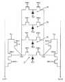
図11及び図12を参照すれば、隣接した4個の距離測定ピクセルZ1〜Z4それぞれは、1つのフォトダイオードPD1〜PD4と、フォトダイオードPD1〜PD4からの電荷が位相差を有して移動する第1トランスファトランジスタTRF1及び第2トランスファトランジスタTRF2とを具備する。 Referring to FIGS. 11 and 12, each of the four adjacent distance measuring pixels Z1 to Z4 moves with one photodiode PD1 to PD4 and charges from the photodiodes PD1 to PD4 having a phase difference. A first transfer transistor TRF1 and a second transfer transistor TRF2 are provided.
距離測定ピクセルZ1〜Z4の第1トランスファトランジスタらTRF1は、第1フローティング拡散領域FD1に並列に連結され、第2トランスファトランジスタTRF2は、第2フローティング拡散領域FD2に並列に連結される。 The first transfer transistors TRF1 of the distance measurement pixels Z1 to Z4 are connected in parallel to the first floating diffusion region FD1, and the second transfer transistor TRF2 is connected in parallel to the second floating diffusion region FD2.
隣接する4個の距離測定ピクセルZ1〜Z4は、第1フローティング拡散領域FD1と連結されたリセットトランジスタRST1、第1フローティング拡散領域FD1にゲートが連結されたドライブトランジスタDRV1;選択トランジスタSEL1;第2フローティング拡散領域FD2と連結されたリセットトランジスタRST2、第2フローティング拡散領域FD2にゲートが連結されたドライブトランジスタDRV2;選択トランジスタSEL2をさらに具備する。 Four adjacent distance measuring pixels Z1 to Z4 include a reset transistor RST1 connected to the first floating diffusion region FD1, a drive transistor DRV1 having a gate connected to the first floating diffusion region FD1, a selection transistor SEL1, and a second floating transistor. It further includes a reset transistor RST2 connected to the diffusion region FD2, a drive transistor DRV2 having a gate connected to the second floating diffusion region FD2, and a selection transistor SEL2.
一方、フォトダイオードPD及びトランスファトランジスタTRF1,TRF2間には、フォトゲートがさらに形成され、便宜上図11では、省略されている。 On the other hand, a photogate is further formed between the photodiode PD and the transfer transistors TRF1 and TRF2, and is omitted in FIG. 11 for convenience.
隣接する4個の距離測定ピクセルZ1〜Z4は、図9のカラーピクセルと比較し、第5スイッチング素子SW5〜第8スイッチング素子SW8と、スイッチング素子SW5〜SW8に連結された統合器INT’と、統合器INT’からの信号が入力される増幅器AMP’とをさらに具備する。統合器INT’からの信号は、第3パスゲート263及び第4パスゲート264に入力され、該パスゲート263,264からの信号は、アナログシグナル処理部(ASP)270、アナログ・デジタルコンバータ(ADC)280及びイメージ信号処理部290に入力される。 Compared with the color pixel of FIG. 9, the four adjacent distance measurement pixels Z1 to Z4 include a fifth switching element SW5 to an eighth switching element SW8, and an integrator INT ′ connected to the switching elements SW5 to SW8. And an amplifier AMP ′ to which a signal from the integrator INT ′ is input. The signal from the integrator INT ′ is input to the
被写体の照度を測定するためには、統合器INTまたは統合器INT’を使用でき、便宜上図12では、統合器INTからの信号のみを利用して照度を判断する。測定された照度判断によって、4個のピクセルを統合して1つの信号として使用することと、それぞれのピクセルを別個の信号として使用することとが決定されうる。 In order to measure the illuminance of the subject, the integrator INT or the integrator INT 'can be used. In FIG. 12, for convenience, the illuminance is determined using only the signal from the integrator INT. Depending on the measured illuminance determination, it can be determined that the four pixels are combined and used as one signal, and each pixel is used as a separate signal.
図12の第1スイッチSW1〜第4スイッチSW4は、第1ピクセル〜第4ピクセルの第1トランスファトランジスタTRF1であって、第5スイッチSW5〜第8スイッチSW8は、第1ピクセル〜第4ピクセルの第2トランスファトランジスタTRF2でありうる。また、第1スイッチSW1〜第8スイッチSW8は、トランスファトランジスタTRF1,TRF2と、第1フローティング拡散領域FD1及び第2フローティング拡散領域FD2との間にそれぞれ形成されたスイッチ(図示せず)でありうる。 The first switch SW1 to the fourth switch SW4 in FIG. 12 are the first transfer transistors TRF1 of the first pixel to the fourth pixel, and the fifth switch SW5 to the eighth switch SW8 are the first to fourth pixels. It may be the second transfer transistor TRF2. Further, the first switch SW1 to the eighth switch SW8 may be switches (not shown) formed between the transfer transistors TRF1 and TRF2 and the first floating diffusion region FD1 and the second floating diffusion region FD2, respectively. .
第1距離測定ピクセルZ1〜第4距離測定ピクセルZ4からの信号がいずれも統合されるためには、第1スイッチSW1〜第4スイッチSW4と第5スイッチSW5〜第8スイッチSW8とがそれぞれ位相差を有していずれも同時にオンさせねばならない。そして、各距離測定ピクセルZ1〜Z4からの信号をそれぞれ得るためには、第1スイッチSW1〜第4スイッチSW4と対応する第5スイッチSW5〜第8スイッチSW8を、順次に位相差を有して時分割器295を使用してターンオンさせねばならない。時分割器295は、ターンオンさせたスイッチSW1〜SW8を知らせる信号をアナログシグナル処理部(ASP)270に入力させる。 In order for all the signals from the first distance measurement pixel Z1 to the fourth distance measurement pixel Z4 to be integrated, the first switch SW1 to the fourth switch SW4 and the fifth switch SW5 to the eighth switch SW8 each have a phase difference. Both of them must be turned on at the same time. In order to obtain signals from the distance measurement pixels Z1 to Z4, the fifth switch SW5 to the eighth switch SW8 corresponding to the first switch SW1 to the fourth switch SW4 are sequentially provided with a phase difference. The
図12の各増幅器AMP,AMP’は、当該ピクセルのドライブトランジスタDRV1,DRV2と選択トランジスタSEL1,SEL2とから構成されうる。 Each of the amplifiers AMP and AMP ′ in FIG. 12 can be composed of drive transistors DRV1 and DRV2 and selection transistors SEL1 and SEL2 of the pixel.
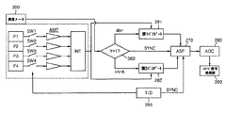
図13は、本発明のさらに他の実施形態によるイメージセンサのブロック図である。 FIG. 13 is a block diagram of an image sensor according to still another embodiment of the present invention.
図13を参照すれば、イメージセンサは、図5のブロック図と比較して、被写体の照度を判断する手段としての照度メータ300と時分割器295とをさらに具備する。照度メータ300は赤外線光を照射し、被写体から反射された赤外線光を受光し、その電気的信号を判断部360に出力する。判断部360は、入力された信号が所定の値以下であると判断されれば、第1パスゲート261を開き、所定の値より大きいに判断すれば、第2パスゲート262を開く。第1パスゲート261がオープンされる場合、時分割器295は、第1スイッチSW1〜第4スイッチSW4をいずれもオンにし、第1パスゲート261には、統合器INTからの統合されたアナログ信号が入力され、該信号は、アナログシグナル処理部(ASP)270に入力される。 Referring to FIG. 13, the image sensor further includes an
第2パスゲート262がオープンされる場合、時分割器295は、第1スイッチング素子SW1〜第4スイッチング素子SW4を順次に開閉し、第1ピクセルP1〜第4ピクセルP4からの電気信号は、統合器INTに順次に入力され、従って、それらの信号は、アナログシグナル処理部(ASP)270に順次に入力される。時分割器295は、アナログシグナル処理部(ASP)270に入力される信号が、ピクセルP1〜P4のうち、いずれの信号からのものであるかを知らせる同期信号SYNCをアナログシグナル処理部(ASP)270に入力する。 When the
アナログシグナル処理部(ASP)270に入力された信号は、アナログ・デジタルコンバータ(ADC)280に入ってデジタル信号に変わり、次に、イメージ信号処理部290に入力される。 The signal input to the analog signal processing unit (ASP) 270 enters the analog / digital converter (ADC) 280 to be converted into a digital signal, and is then input to the image
図14は、本発明のさらに他の実施形態によるイメージセンサのブロック図である。 FIG. 14 is a block diagram of an image sensor according to still another embodiment of the present invention.
図14を参照すれば、イメージセンサは、図9のブロック図と比較して、被写体の照度を判断する手段として照度メータ300を直接具備する。照度メータ300は、被写体に赤外線光を照射し、被写体から反射された光を受光し、その電気的信号を判断部360に出力する。判断部360は、入力された信号が所定の値以下であると判断されれば、第1パスゲート261を開け、所定の値より大きいと判断すれば、第2パスゲート262を開く。時分割器295は、第1スイッチSW1〜第4スイッチSW4をいずれもオンにし、第1パスゲート261には、統合器INTからの統合されたアナログ信号が入力され、該信号は、アナログシグナル処理部(ASP)270に入力される。 Referring to FIG. 14, the image sensor directly includes an
第2パスゲート262がオープンされる場合、時分割器295は、第1スイッチング素子SW1〜第4スイッチング素子SW4を順次に開閉し、第1ピクセルP1〜第4ピクセルP4からの電気信号は、統合器INTに順次に入力され、従って、それらの信号は、アナログシグナル処理部(ASP)270に順次に入力される。 When the
アナログシグナル処理部(ASP)270に入力された信号は、アナログ・デジタルコンバータ(ADC)280に入ってデジタル信号に変わり、次に、イメージ信号処理部290に入力される。 The signal input to the analog signal processing unit (ASP) 270 enters the analog / digital converter (ADC) 280 to be converted into a digital signal, and is then input to the image
図13及び図14の照度メータ300は、図8及び図12の立体イメージセンサにも適用され、詳細な説明は省略する。 The
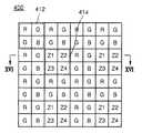
図15は、本発明のさらに他の実施形態による立体イメージセンサのピクセルアレイ400を概略的に示す平面図である。 FIG. 15 is a plan view schematically illustrating a
図15を参照すれば、立体イメージセンサのピクセルアレイ400は、カラーピクセル・パターン412と、距離測定ピクセル・パターン414とを具備する。それらカラーピクセル・パターン412と距離測定ピクセル・パターン414は、アレイ状に配列される。図15では、複数、例えば、3個のカラーピクセル・パターン412が1つの距離測定ピクセル・パターン414に対応するように配列されているが、本発明の実施形態は、必ずしもこれに限定されるものではない。 Referring to FIG. 15, the
カラーピクセル・パターン412は、レッドピクセル(R),グリーンピクセル(G),ブルーピクセル(B)を含む。カラーピクセル・パターンは、図15では、レッドピクセル(R),グリーンピクセル(G),ブルーピクセル(B)を含むが、必ずしもこれに限定されるものではない。例えば、レッドピクセル(R),グリーンピクセル(G),ブルーピクセル(B),マゼンタピクセル(Mg),シアンピクセル(Cy),イエローピクセル(Y),ホワイトピクセル(W)のうち、少なくとも2個のピクセルを含んでなされうる。 The
距離測定ピクセル・パターン414は、例えば、複数の第1距離測定ピクセルZ1〜第4距離測定ピクセルZ4から構成されている。レッドピクセル(R),グリーンピクセル(G),ブルーピクセル(B)と各距離測定ピクセルZ1〜Z4は、実質的に同じサイズに形成されうる。 The distance
図16は、図15のXVI−XVI線に沿って切り取った断面図である。図16を参照すれば、基板420、例えば、p型シリコン基板上に、レッドピクセル(R),グリーンピクセル(G)と距離測定ピクセル(Z1,Z2)とが形成されている。レッドピクセル(R)は、マイクロレンズ430とレッドカラーフィルタ431と光電変換素子432とを具備する。光電変換素子432はn型領域であって、p型基板420と共に、p−n接合フォトダイオードを形成できる。 16 is a cross-sectional view taken along line XVI-XVI in FIG. Referring to FIG. 16, a red pixel (R), a green pixel (G), and distance measuring pixels (Z1, Z2) are formed on a
グリーンピクセル(G)は、マイクロレンズ440とグリーンカラーフィルタ441と光電変換素子442とを具備する。光電変換素子442はn型領域であって、p型基板420と共に、p−n接合フォトダイオードを形成できる。 The green pixel (G) includes a
距離測定ピクセル(Z1,Z2)は、マイクロレンズ450と赤外線フィルタ451と光電変換素子452とを具備する。光電変換素子452はn型領域であって、p型基板と共に、p−n接合フォトダイオードを形成できる。 The distance measurement pixel (Z1, Z2) includes a
ブルーピクセル(B)も、グリーンピクセル(G)及びレッドピクセル(R)と同じ構造を有し、詳細な説明は省略する。 The blue pixel (B) has the same structure as the green pixel (G) and the red pixel (R), and detailed description thereof is omitted.
光電変換素子432,442,452は、基板420に表面から実質的に同じ深さに形成できる。また、マイクロレンズ430,440,450は、実質的に同じサイズに形成されうる。 The
従って、本発明によるピクセルアレイ400を具備したイメージセンサは、従来の半導体工程を使用して容易に、基板420で同じ位置に光電変換素子を形成し、エッチングによって同じサイズのマイクロレンズを製造するので、その工程が容易でありうる。 Accordingly, the image sensor having the
本発明の実施形態によるピクセルアレイ400を具備した立体イメージセンサは、照度が低いときは、距離測定時に4個の距離測定ピクセルZ1〜Z4からの信号を集めて1つの信号データとして使用するので、距離測定感度を向上させることができる。また、照度が高い場合には、距離測定ピクセル(Z)を独立的に、各距離測定ピクセルZ1〜Z4のデータとして使用するので、距離測定解像度を上昇させることができる。そして、カラーピクセルは、それぞれ独立的に配されるので、カラーイメージ解像度が上昇しうる。 The stereoscopic image sensor including the
前記距離測定ピクセル・パターン414は、図7及び図8、図11及び図12に開示された構造を有することができ、詳細な説明は省略する。 The distance measuring
図17は、本発明のさらに他の実施形態による立体イメージセンサのピクセルアレイ500を概略的に示す平面図である。 FIG. 17 is a plan view schematically illustrating a
図17を参照すれば、立体イメージセンサのピクセルアレイ500は、レッドピクセル・パターン511,グリーンピクセル・パターン512,ブルーピクセル・パターン513からなるカラーピクセル・パターンと、距離測定ピクセル・パターン514とを具備する。各ピクセル・パターン511,512,513と距離測定ピクセル・パターン514は、実質的に同じサイズに形成されうる。 Referring to FIG. 17, the
レッドピクセル・パターン511,グリーンピクセル・パターン512,ブルーピクセル・パターン513は、それぞれ4個のレッドピクセル(R),4個のグリーンピクセル(G),4個のブルーピクセル(B)を含む。図17には、各カラーピクセル・パターンが4個のカラーピクセルを具備していると図示しているが、必ずしもこれに限定されるものではない。例えば、各カラーピクセル・パターンは、複数個、例えば、2,3個のカラーピクセルによって形成されもする。 Each of the
カラーピクセル・パターンは、図17ではレッドピクセル(R),グリーンピクセル(G),ブルーピクセル(B)を含むが、必ずしもこれに限定されるものではない。例えば、レッドピクセル(R),グリーンピクセル(G),ブルーピクセル(B),マゼンタピクセル(Mg),シアンピクセル(Cy),イエローピクセル(Y),ホワイトピクセル(W)のうち、3個のピクセルを含んでなされうる。 The color pixel pattern includes a red pixel (R), a green pixel (G), and a blue pixel (B) in FIG. 17, but is not necessarily limited thereto. For example, three pixels among red pixel (R), green pixel (G), blue pixel (B), magenta pixel (Mg), cyan pixel (Cy), yellow pixel (Y), and white pixel (W). Can be made.
距離測定ピクセル・パターン514は、一般的に赤外線光の感度が低く、かつその面積が広いことを考慮し、1つの距離測定ピクセル(Z)によってなっている。 The distance
図18は、図17のXVIII−XVIII線に沿って切り取った断面図である。図18を参照すれば、基板520、例えば、p型シリコン基板上にレッドピクセル・パターン511と距離測定ピクセル・パターン514とが形成されている。レッドピクセル・パターン511は、4個のレッドピクセル(R)にそれぞれ対応する光電変換素子532と、レッドフィルタ531と、レッドピクセル・パターン511に対応する1つのマイクロレンズ530とを具備する。グリーンピクセル・パターン512及びブルーピクセル・パターン513も、レッドピクセル・パターン511と同じ構造によってなっており、詳細な説明は省略する。 18 is a cross-sectional view taken along line XVIII-XVIII in FIG. Referring to FIG. 18, a
距離測定ピクセル・パターン514は、マイクロレンズ540と赤外線フィルタ541と光電変換素子552とを具備する。 The distance
光電変換素子532,542は、基板520に表面から実質的に同じ深さに形成されうる。また、マイクロレンズ530,540は、実質的に同じサイズに形成できる。 The
従って、本発明の実施形態によるピクセルアレイ500を具備したイメージセンサは、従来の半導体工程を使用して容易に、基板520で同じ位置に光電変換素子を形成し、エッチングによって同じサイズのマイクロレンズを製造するので、その工程が容易でありうる。 Accordingly, in the image sensor including the
本発明の実施形態によるピクセルアレイ500を具備したイメージセンサは、照度が低いときは、カラー測定時に、各カラーに対して4個のピクセルからの信号を集めて1つの信号データとして使用するので、カラー感度を向上させることができる。また、照度が高い場合には、4個のピクセルをそれぞれ独立的に使用し、カラーデータとして使用するので、カラー解像度を上昇させることができる。 The image sensor including the
前記カラーピクセル・パターンで、ピクセルの構造は、図5、図6、図9及び図10に開示された構造を有することができ、詳細な説明は省略する。 In the color pixel pattern, the pixel structure may have the structure disclosed in FIGS. 5, 6, 9 and 10, and detailed description thereof will be omitted.
図19は、本発明のさらに他の実施形態による立体イメージセンサのピクセルアレイ600の構造を概略的に示す平面図である。 FIG. 19 is a plan view schematically illustrating a structure of a
図19を参照すれば、ピクセルアレイ600は、カラーピクセル・パターン611と、距離測定ピクセル・パターン614とを具備する。それらカラーピクセル・パターン611と距離測定ピクセル・パターン614は、アレイ状に配列される。図19では、複数、例えば、3個のカラーピクセル・パターン611が1つの距離測定ピクセル・パターン614に対応するように配列されているが、本発明の実施形態は、必ずしもこれに限定されるものではない。 Referring to FIG. 19, the
カラーピクセル・パターン611は、レッドピクセル(R),グリーンピクセル(G),ブルーピクセル(B)を含む。カラーピクセル・パターン611は、図19ではレッドピクセル(R),グリーンピクセル(G),ブルーピクセル(B)を含むが、必ずしもこれに限定されるものではない。例えば、レッドピクセル(R),グリーンピクセル(G),ブルーピクセル(B),マゼンタピクセル(Mg),シアンピクセル(Cy),イエローピクセル(Y),ホワイトピクセル(W)のうち、少なくとも2個のピクセルを含んでなされうる。 The
距離測定ピクセル・パターン614は、1つの距離測定ピクセル(Z)によって構成されている。距離測定ピクセル(Z)は、カラーピクセル・パターン611と実質的に同じサイズに形成されうる。一般的に、距離測定ピクセル(Z)は、赤外線光の感度が低く、かつその面積が広いことを考慮し、カラーピクセルより大きく形成されうる。 The distance measuring
図20は、図19のXX−XX線に沿って切り取った断面図である。図20を参照すれば、基板620、例えば、p型シリコン基板上にカラーピクセル・パターン611と距離測定ピクセル・パターン614とが配列されている。カラーピクセル・パターン611及び距離測定ピクセル・パターン614には、それぞれ1つのマイクロレンズ630,650が配され、各マイクロレンズ630,650は、実質的に同じサイズに形成されうる。 20 is a cross-sectional view taken along line XX-XX in FIG. Referring to FIG. 20, a
カラーピクセル・パターン611のグリーンピクセル(G)とブルーピクセル(B)とが図20に図示されており、他のグリーンピクセル(G)とレッドピクセル(R)は、図20に図示されていないが、その構造は、図示されたグリーンピクセル(G)並びにブルーピクセル(B)と同一である。 The green pixel (G) and the blue pixel (B) of the
1つのマイクロレンズ630の下部には、2つのグリーンフィルタ631と、1つのレッドフィルタ(図示せず)と、1つのブルーフィルタ641とが配される。各フィルタの下部には、対応する光電変換素子632,642が配される。 Two
マイクロレンズ650の下部には、1つの距離測定フィルタ651が配され、距離測定フィルタの下部には、光電変換素子652が配される。 One
光電変換素子632,642,652は、基板620の表面から実質的に同じ深さに形成されうる。また、マイクロレンズ630,650は、実質的に同じサイズに形成されうる。 The
従って、本発明によるイメージセンサ600は、従来の半導体工程を使用して容易に、基板620で同じ位置に光電変換素子を形成し、エッチングによって同じサイズのマイクロレンズを製造するので、その工程が容易でありうる。 Therefore, the
以上、本発明の望ましい実施形態を参照して説明したが、当該技術分野の熟練当業者は、特許請求の範囲に記載された本発明の思想及び領域から外れない範囲内で、本発明を多様に修正及び変更させることができるということを理解することが可能であろう。 Although the present invention has been described with reference to the preferred embodiments, those skilled in the art will recognize that the present invention can be used in various ways without departing from the spirit and scope of the present invention described in the claims. It will be understood that can be modified and changed.
100,200,400,500,600 立体イメージセンサのピクセルアレイ
102 単位ピクセル・パターン
202,431,511,531 レッドピクセル・パターン
204,512 グリーンピクセル・パターン
206,513 ブルーピクセル・パターン
208,414,514,614 距離測定ピクセル・パターン
120,220,420,520,620 基板
130,140,150,230,240,430,440,450,530,540,630,650 マイクロレンズ
131,231,441,631 グリーンフィルタ
132,142,152,232,242,432,442,452,532,542,632,642,652 光電変換素子
141,231 レッドフィルタ
151,241,451,541 赤外線フィルタ
250 比較器
260 判断器
261 第1パスゲート
262 第2パスゲート
263 第3パスゲート
264 第4パスゲート
269 信号処理部
270 アナログシグナル処理部(ASP)
280 アナログ・デジタルコンバータ(ADC)
290 イメージ信号処理部
291 統合出力ライン
293 第1統合出力ライン
294 第2統合出力ライン
295 時分割器
300 照度メータ
360 判断部
412,611 カラーピクセル・パターン
541,651 距離測定フィルタ
641 ブルーフィルタ100, 200, 400, 500, 600 Three-dimensional image
280 Analog to Digital Converter (ADC)
290 Image
Claims (16)
Translated fromJapanese前記カラーピクセルと前記距離測定ピクセルは、実質的に同じサイズに形成されたことを特徴とする請求項5または請求項6に記載の立体イメージセンサのピクセルアレイ。The distance measuring pixel pattern comprises N distance measuring pixels adjacent to each other;
The pixel array of the stereoscopic image sensor according to claim 5, wherein the color pixel and the distance measurement pixel are formed to have substantially the same size.
前記各ピクセルに対応するように形成されたマイクロレンズとを具備し、
前記マイクロレンズは、実質的に同じサイズに形成された立体イメージセンサ。Unit pixel patterns including color pixels and distance measurement pixels are arranged in an array, and the unit pixel patterns are arranged so that the adjacent unit pixel patterns and the distance measurement pixels are adjacent to each other. A pixel array,
A microlens formed to correspond to each pixel,
The microlenses are stereoscopic image sensors formed to have substantially the same size.
Applications Claiming Priority (1)
| Application Number | Priority Date | Filing Date | Title |
|---|---|---|---|
| KR20080077022 | 2008-08-06 |
Publications (1)
| Publication Number | Publication Date |
|---|---|
| JP2010041720Atrue JP2010041720A (en) | 2010-02-18 |
Family
ID=41652564
Family Applications (1)
| Application Number | Title | Priority Date | Filing Date |
|---|---|---|---|
| JP2009176470APendingJP2010041720A (en) | 2008-08-06 | 2009-07-29 | Pixel array of three-dimensional image sensor |
Country Status (4)
| Country | Link |
|---|---|
| US (1) | US20100033611A1 (en) |
| JP (1) | JP2010041720A (en) |
| KR (1) | KR20100018449A (en) |
| CN (1) | CN101651145B (en) |
Cited By (9)
| Publication number | Priority date | Publication date | Assignee | Title |
|---|---|---|---|---|
| WO2012133106A1 (en)* | 2011-03-29 | 2012-10-04 | ソニー株式会社 | Image pickup apparatus, image pickup device, image processing method, aperture control method, and program |
| WO2012140917A1 (en)* | 2011-04-14 | 2012-10-18 | 株式会社ニコン | Image processing apparatus and image processing program |
| JP2012208159A (en)* | 2011-03-29 | 2012-10-25 | Sony Corp | Imaging device, image pickup element, image processing method, and program |
| WO2012164934A1 (en)* | 2011-05-30 | 2012-12-06 | 株式会社ニコン | Image processing device, image processing method, and program |
| JP2013021481A (en)* | 2011-07-11 | 2013-01-31 | Sony Corp | Image processing device and method, and program |
| US9202405B2 (en) | 2014-02-12 | 2015-12-01 | Au Optronics Corporation | Display panel with varied subpixel arrangement sequences |
| WO2016167044A1 (en)* | 2015-04-14 | 2016-10-20 | ソニー株式会社 | Solid-state image pickup device, image pickup system, and distance measurement method |
| WO2021235033A1 (en)* | 2020-05-20 | 2021-11-25 | ソニーグループ株式会社 | Sensing system |
| JP2022050100A (en)* | 2020-09-17 | 2022-03-30 | 株式会社デンソー | Solid-state image sensor |
Families Citing this family (37)
| Publication number | Priority date | Publication date | Assignee | Title |
|---|---|---|---|---|
| US8717417B2 (en) | 2009-04-16 | 2014-05-06 | Primesense Ltd. | Three-dimensional mapping and imaging |
| KR101646908B1 (en)* | 2009-11-27 | 2016-08-09 | 삼성전자주식회사 | Image sensor for sensing object distance information |
| US20110175981A1 (en)* | 2010-01-19 | 2011-07-21 | Chun-Hung Lai | 3d color image sensor |
| TWI531239B (en)* | 2010-05-28 | 2016-04-21 | Hamamatsu Photonics Kk | Solid-state imaging device |
| FR2969819A1 (en)* | 2010-12-22 | 2012-06-29 | St Microelectronics Grenoble 2 | THREE DIMENSIONAL IMAGE SENSOR |
| FR2969822A1 (en) | 2010-12-24 | 2012-06-29 | St Microelectronics Grenoble 2 | THREE DIMENSIONAL IMAGE SENSOR |
| US9030528B2 (en)* | 2011-04-04 | 2015-05-12 | Apple Inc. | Multi-zone imaging sensor and lens array |
| KR101823347B1 (en) | 2011-07-08 | 2018-02-01 | 삼성전자주식회사 | Sensor and data processing system having the same |
| DE102011053219B4 (en) | 2011-09-02 | 2022-03-03 | pmdtechnologies ag | Combined pixel with phase-sensitive and color-selective sub-pixel |
| CN202453582U (en)* | 2012-02-29 | 2012-09-26 | 京东方科技集团股份有限公司 | Pixel structure and display device |
| CN103515371B (en)* | 2012-06-27 | 2016-09-21 | 格科微电子(上海)有限公司 | Integrated-type optical sensor package |
| KR101887988B1 (en) | 2012-07-03 | 2018-08-14 | 삼성전자 주식회사 | Image sensor chip, operation method thereof, and system having the same |
| KR102019186B1 (en)* | 2012-08-16 | 2019-09-06 | 엘지이노텍 주식회사 | Image sensor and camera apparatus having the same |
| KR102019089B1 (en)* | 2012-08-22 | 2019-09-06 | 엘지이노텍 주식회사 | Image sensor and camera apparatus having the same |
| KR101938648B1 (en)* | 2012-10-23 | 2019-01-15 | 삼성전자주식회사 | Mobile system including image sensor, method of operating image sensor and method of operating mobile system |
| KR101932587B1 (en) | 2012-11-20 | 2018-12-26 | 삼성전자주식회사 | Image processing apparatus and method for color-depth demosaicing |
| US20140347442A1 (en)* | 2013-05-23 | 2014-11-27 | Yibing M. WANG | Rgbz pixel arrays, imaging devices, controllers & methods |
| KR102135677B1 (en)* | 2013-11-28 | 2020-07-20 | 삼성전자주식회사 | Image sensor and method of driving image sensor |
| KR101641406B1 (en)* | 2013-12-30 | 2016-07-21 | 연세대학교 산학협력단 | Stereo camera |
| US10002893B2 (en)* | 2014-05-19 | 2018-06-19 | Samsung Electronics Co., Ltd. | Image sensor including hybrid pixel structure |
| KR20160025729A (en)* | 2014-08-28 | 2016-03-09 | 에스케이하이닉스 주식회사 | Image sensor having depth detection pixel and method for depth date generation using the same |
| US9741755B2 (en) | 2014-12-22 | 2017-08-22 | Google Inc. | Physical layout and structure of RGBZ pixel cell unit for RGBZ image sensor |
| US9871065B2 (en) | 2014-12-22 | 2018-01-16 | Google Inc. | RGBZ pixel unit cell with first and second Z transfer gates |
| KR102331920B1 (en)* | 2014-12-26 | 2021-11-29 | 삼성전자주식회사 | Sensor for motion information, illumination information and proximity information, and method for operating processor using the sensor |
| WO2017004834A1 (en) | 2015-07-09 | 2017-01-12 | Huawei Technologies Co., Ltd. | Imaging method, image sensor, and imaging device |
| JP6461429B2 (en) | 2015-12-18 | 2019-01-30 | 広東欧珀移動通信有限公司 | Image sensor, control method, and electronic apparatus |
| US10033949B2 (en) | 2016-06-16 | 2018-07-24 | Semiconductor Components Industries, Llc | Imaging systems with high dynamic range and phase detection pixels |
| KR102667264B1 (en)* | 2016-12-08 | 2024-05-21 | 삼성전자주식회사 | Image sensor having beam splitter |
| KR102406996B1 (en) | 2017-04-07 | 2022-06-08 | 삼성전자주식회사 | Image Sensor |
| US10593712B2 (en)* | 2017-08-23 | 2020-03-17 | Semiconductor Components Industries, Llc | Image sensors with high dynamic range and infrared imaging toroidal pixels |
| US10580807B2 (en) | 2017-10-24 | 2020-03-03 | Stmicroelectronics, Inc. | Color pixel and range pixel combination unit |
| CN108965704B (en)* | 2018-07-19 | 2020-01-31 | 维沃移动通信有限公司 | image sensor, mobile terminal and image shooting method |
| CN108900772A (en)* | 2018-07-19 | 2018-11-27 | 维沃移动通信有限公司 | A kind of mobile terminal and image capturing method |
| WO2021062662A1 (en)* | 2019-09-30 | 2021-04-08 | Oppo广东移动通信有限公司 | Image sensor, camera assembly, and mobile terminal |
| WO2021062661A1 (en) | 2019-09-30 | 2021-04-08 | Oppo广东移动通信有限公司 | Image sensor, camera assembly, and mobile terminal |
| CN113037989B (en)* | 2019-12-09 | 2022-11-18 | 华为技术有限公司 | Image sensor, camera module and control method |
| EP4542984A1 (en)* | 2023-06-23 | 2025-04-23 | Samsung Electronics Co., Ltd | Method and apparatus for generating pattern, and method and apparatus for decoding pattern |
Citations (5)
| Publication number | Priority date | Publication date | Assignee | Title |
|---|---|---|---|---|
| JP2001230966A (en)* | 2000-02-18 | 2001-08-24 | Nikon Gijutsu Kobo:Kk | Electronic camera |
| JP2005134317A (en)* | 2003-10-31 | 2005-05-26 | Canon Inc | Photoelectric conversion device |
| JP2005175392A (en)* | 2003-12-15 | 2005-06-30 | Toshiba Corp | Solid-state imaging device and imaging system using the same |
| JP2007103590A (en)* | 2005-10-03 | 2007-04-19 | Nikon Corp | Imaging device, focus detection apparatus, and imaging system |
| JP2008268112A (en)* | 2007-04-24 | 2008-11-06 | Sanyo Electric Co Ltd | Sensor |
Family Cites Families (6)
| Publication number | Priority date | Publication date | Assignee | Title |
|---|---|---|---|---|
| US143652A (en)* | 1873-10-14 | Improvement in feed-gages for printing-presses | ||
| US8134637B2 (en)* | 2004-01-28 | 2012-03-13 | Microsoft Corporation | Method and system to increase X-Y resolution in a depth (Z) camera using red, blue, green (RGB) sensing |
| US8139130B2 (en)* | 2005-07-28 | 2012-03-20 | Omnivision Technologies, Inc. | Image sensor with improved light sensitivity |
| US7978240B2 (en)* | 2005-10-03 | 2011-07-12 | Konica Minolta Photo Imaging, Inc. | Enhancing image quality imaging unit and image sensor |
| US7821553B2 (en)* | 2005-12-30 | 2010-10-26 | International Business Machines Corporation | Pixel array, imaging sensor including the pixel array and digital camera including the imaging sensor |
| US7375803B1 (en)* | 2006-05-18 | 2008-05-20 | Canesta, Inc. | RGBZ (red, green, blue, z-depth) filter system usable with sensor systems, including sensor systems with synthetic mirror enhanced three-dimensional imaging |
- 2009
- 2009-06-11KRKR1020090051952Apatent/KR20100018449A/ennot_activeWithdrawn
- 2009-07-29JPJP2009176470Apatent/JP2010041720A/enactivePending
- 2009-07-30USUS12/461,063patent/US20100033611A1/ennot_activeAbandoned
- 2009-08-06CNCN2009101657217Apatent/CN101651145B/ennot_activeExpired - Fee Related
Patent Citations (5)
| Publication number | Priority date | Publication date | Assignee | Title |
|---|---|---|---|---|
| JP2001230966A (en)* | 2000-02-18 | 2001-08-24 | Nikon Gijutsu Kobo:Kk | Electronic camera |
| JP2005134317A (en)* | 2003-10-31 | 2005-05-26 | Canon Inc | Photoelectric conversion device |
| JP2005175392A (en)* | 2003-12-15 | 2005-06-30 | Toshiba Corp | Solid-state imaging device and imaging system using the same |
| JP2007103590A (en)* | 2005-10-03 | 2007-04-19 | Nikon Corp | Imaging device, focus detection apparatus, and imaging system |
| JP2008268112A (en)* | 2007-04-24 | 2008-11-06 | Sanyo Electric Co Ltd | Sensor |
Cited By (25)
| Publication number | Priority date | Publication date | Assignee | Title |
|---|---|---|---|---|
| WO2012133106A1 (en)* | 2011-03-29 | 2012-10-04 | ソニー株式会社 | Image pickup apparatus, image pickup device, image processing method, aperture control method, and program |
| JP2012208159A (en)* | 2011-03-29 | 2012-10-25 | Sony Corp | Imaging device, image pickup element, image processing method, and program |
| US10397547B2 (en) | 2011-03-29 | 2019-08-27 | Sony Corporation | Stereoscopic image pickup unit, image pickup device, picture processing method, control method, and program utilizing diaphragm to form pair of apertures |
| US9544571B2 (en) | 2011-03-29 | 2017-01-10 | Sony Corporation | Image pickup unit, image pickup device, picture processing method, diaphragm control method, and program |
| US9826215B2 (en) | 2011-03-29 | 2017-11-21 | Sony Corporation | Stereoscopic image pickup unit, image pickup device, picture processing method, control method, and program utilizing diaphragm to form pair of apertures |
| WO2012140917A1 (en)* | 2011-04-14 | 2012-10-18 | 株式会社ニコン | Image processing apparatus and image processing program |
| JPWO2012140917A1 (en)* | 2011-04-14 | 2014-07-28 | 株式会社ニコン | Image processing apparatus and image processing program |
| WO2012164934A1 (en)* | 2011-05-30 | 2012-12-06 | 株式会社ニコン | Image processing device, image processing method, and program |
| JP2013021481A (en)* | 2011-07-11 | 2013-01-31 | Sony Corp | Image processing device and method, and program |
| US9083957B2 (en) | 2011-07-11 | 2015-07-14 | Sony Corporation | Image processing apparatus, image processing method, and program |
| US9538163B2 (en) | 2011-07-11 | 2017-01-03 | Sony Corporation | Image processing apparatus, image processing method, and program |
| US9202405B2 (en) | 2014-02-12 | 2015-12-01 | Au Optronics Corporation | Display panel with varied subpixel arrangement sequences |
| JPWO2016167044A1 (en)* | 2015-04-14 | 2018-02-08 | ソニー株式会社 | Solid-state imaging device, imaging system, and distance measuring method |
| WO2016167044A1 (en)* | 2015-04-14 | 2016-10-20 | ソニー株式会社 | Solid-state image pickup device, image pickup system, and distance measurement method |
| US20200120300A1 (en)* | 2015-04-14 | 2020-04-16 | Sony Corporation | Solid-state imaging apparatus, imaging system, and distance measurement method |
| JP2020188275A (en)* | 2015-04-14 | 2020-11-19 | ソニー株式会社 | Solid-state image sensor, image sensor and distance measurement method |
| US11076115B2 (en) | 2015-04-14 | 2021-07-27 | Sony Corporation | Solid-state imaging apparatus, imaging system, and distance measurement method |
| US11128828B2 (en)* | 2015-04-14 | 2021-09-21 | Sony Corporation | Solid-state imaging apparatus, imaging system, and distance measurement method |
| JP7124849B2 (en) | 2015-04-14 | 2022-08-24 | ソニーグループ株式会社 | Solid-state imaging device, imaging system, and distance measurement method |
| US11818486B2 (en) | 2015-04-14 | 2023-11-14 | Sony Group Corporation | Solid-state imaging apparatus, imaging system, and distance measurement methods |
| WO2021235033A1 (en)* | 2020-05-20 | 2021-11-25 | ソニーグループ株式会社 | Sensing system |
| JPWO2021235033A1 (en)* | 2020-05-20 | 2021-11-25 | ||
| JP7609162B2 (en) | 2020-05-20 | 2025-01-07 | ソニーグループ株式会社 | Sensing System |
| JP2022050100A (en)* | 2020-09-17 | 2022-03-30 | 株式会社デンソー | Solid-state image sensor |
| JP7459739B2 (en) | 2020-09-17 | 2024-04-02 | 株式会社デンソー | solid-state image sensor |
Also Published As
| Publication number | Publication date |
|---|---|
| KR20100018449A (en) | 2010-02-17 |
| CN101651145A (en) | 2010-02-17 |
| US20100033611A1 (en) | 2010-02-11 |
| CN101651145B (en) | 2013-09-25 |
Similar Documents
| Publication | Publication Date | Title |
|---|---|---|
| JP2010041720A (en) | Pixel array of three-dimensional image sensor | |
| JP6110891B2 (en) | Pixel binning in image sensors | |
| JP2010081609A (en) | Solid image sensor | |
| US9596423B1 (en) | Charge summing in an image sensor | |
| JP6885344B2 (en) | Solid-state image sensor, its driving method, and electronic devices | |
| TWI581415B (en) | Virtual high dynamic range size pixel image sensor | |
| US6958862B1 (en) | Use of a lenslet array with a vertically stacked pixel array | |
| JP5331107B2 (en) | Imaging device | |
| CN102348075B (en) | There is dual-element color filter array and the imageing sensor of three channel colours output | |
| KR20180013877A (en) | Semiconductor device and electronic apparatus | |
| JP2009529291A (en) | Combined multi-array color image sensor | |
| JP2006332602A (en) | Image sensor for semiconductor photosensitive device and image sensor processing apparatus using the same. | |
| CN110649057A (en) | Image sensor, camera assembly and mobile terminal | |
| EP4033535A1 (en) | Image sensor, camera assembly and mobile terminal | |
| JP2011166477A (en) | Solid-state imaging element and image input device | |
| JP2006165362A (en) | Solid-state image sensor | |
| KR20160072508A (en) | Color filter array and image sensor having the same | |
| JP2014075767A (en) | Solid-state imaging device | |
| JP6245942B2 (en) | Image sensor | |
| JP5365667B2 (en) | Semiconductor image sensor | |
| JP5103341B2 (en) | Solid-state imaging device and imaging apparatus | |
| KR20090034479A (en) | Image sensor and manufacturing method | |
| HK1212510B (en) | Color image sensor with metal mesh to detect infrared light | |
| HK1212510A1 (en) | Color image sensor with metal mesh to detect infrared light |
Legal Events
| Date | Code | Title | Description |
|---|---|---|---|
| A621 | Written request for application examination | Free format text:JAPANESE INTERMEDIATE CODE: A621 Effective date:20120521 | |
| A977 | Report on retrieval | Free format text:JAPANESE INTERMEDIATE CODE: A971007 Effective date:20130808 | |
| A131 | Notification of reasons for refusal | Free format text:JAPANESE INTERMEDIATE CODE: A131 Effective date:20130910 | |
| A521 | Request for written amendment filed | Free format text:JAPANESE INTERMEDIATE CODE: A523 Effective date:20131209 | |
| A131 | Notification of reasons for refusal | Free format text:JAPANESE INTERMEDIATE CODE: A131 Effective date:20140107 | |
| A02 | Decision of refusal | Free format text:JAPANESE INTERMEDIATE CODE: A02 Effective date:20140609 |