JP2010034254A - Three-dimensional large-scale integrated circuit (lsi) - Google Patents
Three-dimensional large-scale integrated circuit (lsi)Download PDFInfo
- Publication number
- JP2010034254A JP2010034254AJP2008194408AJP2008194408AJP2010034254AJP 2010034254 AJP2010034254 AJP 2010034254AJP 2008194408 AJP2008194408 AJP 2008194408AJP 2008194408 AJP2008194408 AJP 2008194408AJP 2010034254 AJP2010034254 AJP 2010034254A
- Authority
- JP
- Japan
- Prior art keywords
- integrated circuit
- dimensional
- adhesive layer
- dimensional integrated
- lsi
- Prior art date
- Legal status (The legal status is an assumption and is not a legal conclusion. Google has not performed a legal analysis and makes no representation as to the accuracy of the status listed.)
- Pending
Links
- 239000010410layerSubstances0.000claimsabstractdescription87
- 239000012790adhesive layerSubstances0.000claimsabstractdescription65
- 238000000034methodMethods0.000abstractdescription16
- 230000017525heat dissipationEffects0.000abstractdescription6
- 229920005989resinPolymers0.000description23
- 239000011347resinSubstances0.000description23
- 239000000758substrateSubstances0.000description21
- 239000002861polymer materialSubstances0.000description20
- 239000011231conductive fillerSubstances0.000description18
- 238000001723curingMethods0.000description18
- 239000000463materialSubstances0.000description17
- 239000011342resin compositionSubstances0.000description14
- 238000000576coating methodMethods0.000description12
- 239000003795chemical substances by applicationSubstances0.000description10
- 229910052751metalInorganic materials0.000description9
- 239000002184metalSubstances0.000description9
- 229920002725thermoplastic elastomerPolymers0.000description7
- 229920001187thermosetting polymerPolymers0.000description7
- 239000011248coating agentSubstances0.000description6
- 229920001971elastomerPolymers0.000description6
- 239000010408filmSubstances0.000description6
- -1polyethylenePolymers0.000description6
- OKTJSMMVPCPJKN-UHFFFAOYSA-NCarbonChemical compound[C]OKTJSMMVPCPJKN-UHFFFAOYSA-N0.000description5
- 239000000203mixtureSubstances0.000description5
- 229920001955polyphenylene etherPolymers0.000description5
- 239000005060rubberSubstances0.000description5
- 239000004642PolyimideSubstances0.000description4
- 229910052802copperInorganic materials0.000description4
- 239000010949copperSubstances0.000description4
- 239000003822epoxy resinSubstances0.000description4
- 150000004767nitridesChemical class0.000description4
- 229920000647polyepoxidePolymers0.000description4
- 229920001721polyimidePolymers0.000description4
- 238000007711solidificationMethods0.000description4
- 230000008023solidificationEffects0.000description4
- 229910052582BNInorganic materials0.000description3
- PZNSFCLAULLKQX-UHFFFAOYSA-NBoron nitrideChemical compoundN#BPZNSFCLAULLKQX-UHFFFAOYSA-N0.000description3
- RYGMFSIKBFXOCR-UHFFFAOYSA-NCopperChemical compound[Cu]RYGMFSIKBFXOCR-UHFFFAOYSA-N0.000description3
- PXHVJJICTQNCMI-UHFFFAOYSA-NNickelChemical compound[Ni]PXHVJJICTQNCMI-UHFFFAOYSA-N0.000description3
- XUIMIQQOPSSXEZ-UHFFFAOYSA-NSiliconChemical compound[Si]XUIMIQQOPSSXEZ-UHFFFAOYSA-N0.000description3
- 239000000853adhesiveSubstances0.000description3
- 230000001070adhesive effectEffects0.000description3
- 229910052782aluminiumInorganic materials0.000description3
- 229910052799carbonInorganic materials0.000description3
- PMHQVHHXPFUNSP-UHFFFAOYSA-Mcopper(1+);methylsulfanylmethane;bromideChemical compoundBr[Cu].CSCPMHQVHHXPFUNSP-UHFFFAOYSA-M0.000description3
- 230000000694effectsEffects0.000description3
- 239000000835fiberSubstances0.000description3
- 238000003475laminationMethods0.000description3
- 229910044991metal oxideInorganic materials0.000description3
- 150000004706metal oxidesChemical class0.000description3
- 238000013008moisture curingMethods0.000description3
- 230000000149penetrating effectEffects0.000description3
- 229910052710siliconInorganic materials0.000description3
- 239000010703siliconSubstances0.000description3
- 229910052709silverInorganic materials0.000description3
- 239000004332silverSubstances0.000description3
- 239000004925Acrylic resinSubstances0.000description2
- 229920000178Acrylic resinPolymers0.000description2
- YCKRFDGAMUMZLT-UHFFFAOYSA-NFluorine atomChemical compound[F]YCKRFDGAMUMZLT-UHFFFAOYSA-N0.000description2
- 229920000459Nitrile rubberPolymers0.000description2
- BQCADISMDOOEFD-UHFFFAOYSA-NSilverChemical compound[Ag]BQCADISMDOOEFD-UHFFFAOYSA-N0.000description2
- PPBRXRYQALVLMV-UHFFFAOYSA-NStyreneChemical compoundC=CC1=CC=CC=C1PPBRXRYQALVLMV-UHFFFAOYSA-N0.000description2
- XLOMVQKBTHCTTD-UHFFFAOYSA-NZinc monoxideChemical compound[Zn]=OXLOMVQKBTHCTTD-UHFFFAOYSA-N0.000description2
- 239000006096absorbing agentSubstances0.000description2
- 229910045601alloyInorganic materials0.000description2
- 239000000956alloySubstances0.000description2
- XAGFODPZIPBFFR-UHFFFAOYSA-NaluminiumChemical compound[Al]XAGFODPZIPBFFR-UHFFFAOYSA-N0.000description2
- 239000003963antioxidant agentSubstances0.000description2
- 239000002216antistatic agentSubstances0.000description2
- 230000015572biosynthetic processEffects0.000description2
- 238000013329compoundingMethods0.000description2
- 229920001577copolymerPolymers0.000description2
- 238000004132cross linkingMethods0.000description2
- 239000002270dispersing agentSubstances0.000description2
- 239000000975dyeSubstances0.000description2
- 230000005684electric fieldEffects0.000description2
- 239000000945fillerSubstances0.000description2
- 239000011737fluorineSubstances0.000description2
- 229910052731fluorineInorganic materials0.000description2
- 239000011521glassSubstances0.000description2
- 229910052737goldInorganic materials0.000description2
- 239000010931goldSubstances0.000description2
- 239000000314lubricantSubstances0.000description2
- 150000001247metal acetylidesChemical class0.000description2
- 229910000000metal hydroxideInorganic materials0.000description2
- 150000004692metal hydroxidesChemical class0.000description2
- 150000002739metalsChemical class0.000description2
- 238000002156mixingMethods0.000description2
- 229910052759nickelInorganic materials0.000description2
- 239000000049pigmentSubstances0.000description2
- 239000004014plasticizerSubstances0.000description2
- BASFCYQUMIYNBI-UHFFFAOYSA-NplatinumChemical compound[Pt]BASFCYQUMIYNBI-UHFFFAOYSA-N0.000description2
- 229920000642polymerPolymers0.000description2
- 229920002635polyurethanePolymers0.000description2
- 239000004814polyurethaneSubstances0.000description2
- 230000005855radiationEffects0.000description2
- 239000012779reinforcing materialSubstances0.000description2
- 238000007650screen-printingMethods0.000description2
- 239000004065semiconductorSubstances0.000description2
- 239000002904solventSubstances0.000description2
- 239000003381stabilizerSubstances0.000description2
- 229920003048styrene butadiene rubberPolymers0.000description2
- 239000003017thermal stabilizerSubstances0.000description2
- 229920005992thermoplastic resinPolymers0.000description2
- 239000010409thin filmSubstances0.000description2
- XQUPVDVFXZDTLT-UHFFFAOYSA-N1-[4-[[4-(2,5-dioxopyrrol-1-yl)phenyl]methyl]phenyl]pyrrole-2,5-dioneChemical compoundO=C1C=CC(=O)N1C(C=C1)=CC=C1CC1=CC=C(N2C(C=CC2=O)=O)C=C1XQUPVDVFXZDTLT-UHFFFAOYSA-N0.000description1
- 239000004953Aliphatic polyamideSubstances0.000description1
- 229920000049Carbon (fiber)Polymers0.000description1
- 239000004709Chlorinated polyethyleneSubstances0.000description1
- 229920000089Cyclic olefin copolymerPolymers0.000description1
- 239000004641Diallyl-phthalateSubstances0.000description1
- 244000043261Hevea brasiliensisSpecies0.000description1
- 229920000106Liquid crystal polymerPolymers0.000description1
- 239000004977Liquid-crystal polymers (LCPs)Substances0.000description1
- 239000002033PVDF binderSubstances0.000description1
- 229920002845Poly(methacrylic acid)Polymers0.000description1
- 229930182556PolyacetalNatural products0.000description1
- 239000004962Polyamide-imideSubstances0.000description1
- 239000005062PolybutadieneSubstances0.000description1
- 239000004695Polyether sulfoneSubstances0.000description1
- 239000004698PolyethyleneSubstances0.000description1
- 239000004721Polyphenylene oxideSubstances0.000description1
- 239000004734Polyphenylene sulfideSubstances0.000description1
- 239000004743PolypropyleneSubstances0.000description1
- 239000004793PolystyreneSubstances0.000description1
- 239000004372Polyvinyl alcoholSubstances0.000description1
- 229920001328Polyvinylidene chloridePolymers0.000description1
- 229910052581Si3N4Inorganic materials0.000description1
- 229920002125Sokalan®Polymers0.000description1
- 229920006311Urethane elastomerPolymers0.000description1
- BZHJMEDXRYGGRV-UHFFFAOYSA-NVinyl chlorideChemical compoundClC=CBZHJMEDXRYGGRV-UHFFFAOYSA-N0.000description1
- 125000005396acrylic acid ester groupChemical group0.000description1
- 229920000122acrylonitrile butadiene styrenePolymers0.000description1
- 229920003231aliphatic polyamidePolymers0.000description1
- 150000001336alkenesChemical class0.000description1
- WNROFYMDJYEPJX-UHFFFAOYSA-Kaluminium hydroxideChemical compound[OH-].[OH-].[OH-].[Al+3]WNROFYMDJYEPJX-UHFFFAOYSA-K0.000description1
- 239000004760aramidSubstances0.000description1
- 229920003235aromatic polyamidePolymers0.000description1
- 229910021383artificial graphiteInorganic materials0.000description1
- UMIVXZPTRXBADB-UHFFFAOYSA-NbenzocyclobuteneChemical compoundC1=CC=C2CCC2=C1UMIVXZPTRXBADB-UHFFFAOYSA-N0.000description1
- QUDWYFHPNIMBFC-UHFFFAOYSA-Nbis(prop-2-enyl) benzene-1,2-dicarboxylateChemical compoundC=CCOC(=O)C1=CC=CC=C1C(=O)OCC=CQUDWYFHPNIMBFC-UHFFFAOYSA-N0.000description1
- 229920005549butyl rubberPolymers0.000description1
- 239000004917carbon fiberSubstances0.000description1
- 229910021393carbon nanotubeInorganic materials0.000description1
- 239000002041carbon nanotubeSubstances0.000description1
- 239000004020conductorSubstances0.000description1
- 239000013078crystalSubstances0.000description1
- 239000000806elastomerSubstances0.000description1
- 239000005038ethylene vinyl acetateSubstances0.000description1
- PCHJSUWPFVWCPO-UHFFFAOYSA-NgoldChemical compound[Au]PCHJSUWPFVWCPO-UHFFFAOYSA-N0.000description1
- 229910002804graphiteInorganic materials0.000description1
- 239000010439graphiteSubstances0.000description1
- 239000011357graphitized carbon fiberSubstances0.000description1
- 229920005555halobutylPolymers0.000description1
- 238000005338heat storageMethods0.000description1
- 238000010438heat treatmentMethods0.000description1
- 229920002681hypalonPolymers0.000description1
- 238000009413insulationMethods0.000description1
- 239000012212insulatorSubstances0.000description1
- 230000010354integrationEffects0.000description1
- 229920000554ionomerPolymers0.000description1
- 229920003049isoprene rubberPolymers0.000description1
- 239000007788liquidSubstances0.000description1
- VTHJTEIRLNZDEV-UHFFFAOYSA-Lmagnesium dihydroxideChemical compound[OH-].[OH-].[Mg+2]VTHJTEIRLNZDEV-UHFFFAOYSA-L0.000description1
- 239000000347magnesium hydroxideSubstances0.000description1
- 229910001862magnesium hydroxideInorganic materials0.000description1
- 239000000395magnesium oxideSubstances0.000description1
- CPLXHLVBOLITMK-UHFFFAOYSA-Nmagnesium oxideInorganic materials[Mg]=OCPLXHLVBOLITMK-UHFFFAOYSA-N0.000description1
- AXZKOIWUVFPNLO-UHFFFAOYSA-Nmagnesium;oxygen(2-)Chemical compound[O-2].[Mg+2]AXZKOIWUVFPNLO-UHFFFAOYSA-N0.000description1
- 238000004519manufacturing processMethods0.000description1
- 239000002931mesocarbon microbeadSubstances0.000description1
- 239000007769metal materialSubstances0.000description1
- 239000002116nanohornSubstances0.000description1
- 229920003052natural elastomerPolymers0.000description1
- 229910021382natural graphiteInorganic materials0.000description1
- 229920001194natural rubberPolymers0.000description1
- 150000002825nitrilesChemical class0.000description1
- JRZJOMJEPLMPRA-UHFFFAOYSA-NolefinNatural productsCCCCCCCC=CJRZJOMJEPLMPRA-UHFFFAOYSA-N0.000description1
- TWNQGVIAIRXVLR-UHFFFAOYSA-Noxo(oxoalumanyloxy)alumaneChemical compoundO=[Al]O[Al]=OTWNQGVIAIRXVLR-UHFFFAOYSA-N0.000description1
- 239000002245particleSubstances0.000description1
- 230000002093peripheral effectEffects0.000description1
- 239000005011phenolic resinSubstances0.000description1
- 238000000016photochemical curingMethods0.000description1
- 229910052697platinumInorganic materials0.000description1
- 229920003192poly(bis maleimide)Polymers0.000description1
- 229920001084poly(chloroprene)Polymers0.000description1
- 229920001643poly(ether ketone)Polymers0.000description1
- 229920003207poly(ethylene-2,6-naphthalate)Polymers0.000description1
- 229920001200poly(ethylene-vinyl acetate)Polymers0.000description1
- 229920003229poly(methyl methacrylate)Polymers0.000description1
- 229920002285poly(styrene-co-acrylonitrile)Polymers0.000description1
- 229920002492poly(sulfone)Polymers0.000description1
- 229920002239polyacrylonitrilePolymers0.000description1
- 229920002647polyamidePolymers0.000description1
- 229920002312polyamide-imidePolymers0.000description1
- 229920002577polybenzoxazolePolymers0.000description1
- 229920002857polybutadienePolymers0.000description1
- 229920001707polybutylene terephthalatePolymers0.000description1
- 229920000515polycarbonatePolymers0.000description1
- 239000004417polycarbonateSubstances0.000description1
- 229910021420polycrystalline siliconInorganic materials0.000description1
- 229920000728polyesterPolymers0.000description1
- 229920000570polyetherPolymers0.000description1
- 229920006393polyether sulfonePolymers0.000description1
- 229920000573polyethylenePolymers0.000description1
- 239000011112polyethylene naphthalateSubstances0.000description1
- 229920000139polyethylene terephthalatePolymers0.000description1
- 239000005020polyethylene terephthalateSubstances0.000description1
- 229920001470polyketonePolymers0.000description1
- 239000004926polymethyl methacrylateSubstances0.000description1
- 229920000306polymethylpentenePolymers0.000description1
- 239000011116polymethylpenteneSubstances0.000description1
- 229920006324polyoxymethylenePolymers0.000description1
- 229920000069polyphenylene sulfidePolymers0.000description1
- 229920001155polypropylenePolymers0.000description1
- 229920005591polysiliconPolymers0.000description1
- 229920001296polysiloxanePolymers0.000description1
- 229920002223polystyrenePolymers0.000description1
- 229920000346polystyrene-polyisoprene block-polystyrenePolymers0.000description1
- 229920001343polytetrafluoroethylenePolymers0.000description1
- 239000004810polytetrafluoroethyleneSubstances0.000description1
- 229920002689polyvinyl acetatePolymers0.000description1
- 239000011118polyvinyl acetateSubstances0.000description1
- 229920002451polyvinyl alcoholPolymers0.000description1
- 229920000915polyvinyl chloridePolymers0.000description1
- 239000004800polyvinyl chlorideSubstances0.000description1
- 239000005033polyvinylidene chlorideSubstances0.000description1
- 229920002981polyvinylidene fluoridePolymers0.000description1
- 229910010271silicon carbideInorganic materials0.000description1
- HBMJWWWQQXIZIP-UHFFFAOYSA-Nsilicon carbideChemical compound[Si+]#[C-]HBMJWWWQQXIZIP-UHFFFAOYSA-N0.000description1
- HQVNEWCFYHHQES-UHFFFAOYSA-Nsilicon nitrideChemical compoundN12[Si]34N5[Si]62N3[Si]51N64HQVNEWCFYHHQES-UHFFFAOYSA-N0.000description1
- 229920002050silicone resinPolymers0.000description1
- 229920002379silicone rubberPolymers0.000description1
- 239000004945silicone rubberSubstances0.000description1
- 239000000126substanceSubstances0.000description1
- 229920001169thermoplasticPolymers0.000description1
- 239000004416thermosoftening plasticSubstances0.000description1
- 229910052721tungstenInorganic materials0.000description1
- UONOETXJSWQNOL-UHFFFAOYSA-Ntungsten carbideChemical compound[W+]#[C-]UONOETXJSWQNOL-UHFFFAOYSA-N0.000description1
- 229920006337unsaturated polyester resinPolymers0.000description1
- 238000007740vapor depositionMethods0.000description1
- XLYOFNOQVPJJNP-UHFFFAOYSA-NwaterSubstancesOXLYOFNOQVPJJNP-UHFFFAOYSA-N0.000description1
- 239000011787zinc oxideSubstances0.000description1
- 229910052845zirconInorganic materials0.000description1
- GFQYVLUOOAAOGM-UHFFFAOYSA-Nzirconium(iv) silicateChemical compound[Zr+4].[O-][Si]([O-])([O-])[O-]GFQYVLUOOAAOGM-UHFFFAOYSA-N0.000description1
- 239000004711α-olefinSubstances0.000description1
Images


Classifications
- H—ELECTRICITY
- H01—ELECTRIC ELEMENTS
- H01L—SEMICONDUCTOR DEVICES NOT COVERED BY CLASS H10
- H01L2224/00—Indexing scheme for arrangements for connecting or disconnecting semiconductor or solid-state bodies and methods related thereto as covered by H01L24/00
- H01L2224/01—Means for bonding being attached to, or being formed on, the surface to be connected, e.g. chip-to-package, die-attach, "first-level" interconnects; Manufacturing methods related thereto
- H01L2224/10—Bump connectors; Manufacturing methods related thereto
- H01L2224/15—Structure, shape, material or disposition of the bump connectors after the connecting process
- H01L2224/16—Structure, shape, material or disposition of the bump connectors after the connecting process of an individual bump connector
- H01L2224/161—Disposition
- H01L2224/16135—Disposition the bump connector connecting between different semiconductor or solid-state bodies, i.e. chip-to-chip
- H01L2224/16145—Disposition the bump connector connecting between different semiconductor or solid-state bodies, i.e. chip-to-chip the bodies being stacked
Landscapes
- Cooling Or The Like Of Semiconductors Or Solid State Devices (AREA)
Abstract
Translated fromJapaneseDescription
Translated fromJapanese本発明は、二次元集積回路層を多数積層した高密度な三次元LSIに関する。 The present invention relates to a high-density three-dimensional LSI in which a number of two-dimensional integrated circuit layers are stacked.
近年の電子機器の小型化、高機能化に伴い、これらに搭載されるLSI(半導体集積性回路装置)の高密度化、高集積化が求められている。
これまでは、主として回路の微細化によってLSIの高密度化、高集積化が図られてきたが、最近になって、LSIの三次元化による方法も提案されつつある(例えば特許文献1、特許文献2、特許文献3等参照)。三次元LSIでは、Si等の基板上に二次元集積回路を形成したチップを積層するが、このような三次元LSIにおいては、各二次元集積回路層から発生した熱が放熱されにくく、内部に蓄熱されやすいという課題があった。
Until now, LSIs have been mainly densified and highly integrated by circuit miniaturization, but recently, a method using three-dimensional LSIs has also been proposed (for example,
このような課題を解決するため、従来のLSIチップを積層した3次元LSIにおいては、高熱伝導性のSi等の基板から熱を逃がす設計が考えられていた。
しかしながら、このような方法で三次元回路を形成するには、基板を貫通する配線が必要であるため、その加工性から基板の薄化が求められており、さらには、基板の代わりに、接着層上にSi等の薄層を成膜して用いることも考えられている。したがってSi等の基板から熱を逃がすことは困難になりつつある。In order to solve such a problem, in a conventional three-dimensional LSI in which LSI chips are stacked, a design for releasing heat from a substrate having high thermal conductivity such as Si has been considered.
However, in order to form a three-dimensional circuit by such a method, a wiring penetrating the substrate is required. Therefore, thinning of the substrate is required from the workability, and further, an adhesive is used instead of the substrate. It is also considered that a thin layer such as Si is formed on the layer. Therefore, it is becoming difficult to release heat from a substrate such as Si.
そこで、本発明では、多数の二次元集積回路層を積層した場合であっても、各二次元集積回路層から発生する熱を外部に放熱可能であり、三次元LSIの薄型化が可能、かつ簡便な工程で製造可能な三次元LSIを提供することを目的とする。 Therefore, in the present invention, even when a large number of two-dimensional integrated circuit layers are stacked, the heat generated from each two-dimensional integrated circuit layer can be dissipated to the outside, and the three-dimensional LSI can be thinned. It is an object to provide a three-dimensional LSI that can be manufactured by a simple process.
本発明者らは、上記課題を解決すべく鋭意検討した結果、複数の二次元集積回路層を接着するために用いられる接着層の接着面に平行方向の熱伝導性を、積層面に垂直方向の熱伝導性より高いものとすることにより、各二次元集積回路層から発生する熱を、接着層のエッジ側から三次元LSIの外部に放熱することが可能であることを見出した。さらに、このような構成とすれば、多数の二次元集積回路層を積層する場合においても、別途放熱のための部材等を設ける必要が少なく、簡便な工程で三次元LSIを製造可能であり、また三次元LSIを薄型化可能であることも見出した。 As a result of intensive studies to solve the above problems, the present inventors have determined that the thermal conductivity in the direction parallel to the bonding surface of the bonding layer used for bonding a plurality of two-dimensional integrated circuit layers is perpendicular to the stacking surface. It has been found that heat generated from each two-dimensional integrated circuit layer can be dissipated from the edge side of the adhesive layer to the outside of the three-dimensional LSI by making the heat conductivity higher than that of the three-dimensional LSI. Furthermore, with such a configuration, even when a large number of two-dimensional integrated circuit layers are stacked, it is not necessary to provide a separate member for heat dissipation, and a three-dimensional LSI can be manufactured by a simple process. It has also been found that the three-dimensional LSI can be thinned.
本発明の要旨は、第一の二次元集積回路層と、絶縁性の接着層と、第二の二次元集積回路層とをこの順に備え、該接着層の積層面に平行方向の熱伝導性が、積層面に垂直方向の熱伝導性よりも高いことを特徴とする三次元LSIに存する。
また、該接着層の積層面に平行方向の熱伝導性が1.0W/m・K以上であることが好ましい。The gist of the present invention is that a first two-dimensional integrated circuit layer, an insulating adhesive layer, and a second two-dimensional integrated circuit layer are provided in this order, and the thermal conductivity in the direction parallel to the laminated surface of the adhesive layer However, the present invention resides in a three-dimensional LSI characterized by higher thermal conductivity in the direction perpendicular to the laminated surface.
The thermal conductivity in the direction parallel to the laminated surface of the adhesive layer is preferably 1.0 W / m · K or more.
この際、該接着層の厚さが1μm以上50μm以下であることが好ましい。
また上記三次元LSIは、該第一の二次元集積回路層、該接着層、及び該第二の二次元集積回路層を、各層の積層面に垂直方向に導通する高熱伝導性部材を備えることが好ましい。この高熱伝導性部材は、二次元集積回路のいずれの場所にあっても良く、外周部にあっても、内部にあって三次元LSIの外表面側に設けられる放熱部等と導通する構造としても良い。また、高熱伝導性部材は三次元LSI内の回路から独立していてもよく、また配線の一部を兼ねていても良い。
また、積層される二次元集積回路層の数が3以上であることが好ましい。At this time, the thickness of the adhesive layer is preferably 1 μm or more and 50 μm or less.
In addition, the three-dimensional LSI includes a high thermal conductive member that conducts the first two-dimensional integrated circuit layer, the adhesive layer, and the second two-dimensional integrated circuit layer in a direction perpendicular to the laminated surface of each layer. Is preferred. This high thermal conductivity member may be located anywhere in the two-dimensional integrated circuit, and has a structure that is electrically connected to a heat radiating portion provided on the outer surface side of the three-dimensional LSI, even in the outer peripheral portion. Also good. Further, the high thermal conductivity member may be independent from the circuit in the three-dimensional LSI, or may also serve as part of the wiring.
Moreover, it is preferable that the number of two-dimensional integrated circuit layers to be stacked is three or more.
本発明によれば、各二次元集積回路層から発生する熱を、これらの二次元集積回路層を接着するための接着層のエッジ側等から放熱することが可能となる。したがって、三次元LSIが多数の二次元集積回路層を有する場合であっても、簡便な工程で、放熱性に優れた三次元LSIを形成することが可能であり、また別途、放熱のための機構を設ける必要が少ないことから、三次元LSIを薄型化することも可能となる。 According to the present invention, it is possible to dissipate heat generated from each two-dimensional integrated circuit layer from the edge side of the adhesive layer for bonding these two-dimensional integrated circuit layers. Therefore, even when the three-dimensional LSI has a large number of two-dimensional integrated circuit layers, it is possible to form a three-dimensional LSI with excellent heat dissipation by a simple process. Since there is little need to provide a mechanism, the three-dimensional LSI can be thinned.
以下、本発明について詳しく説明するが、本発明は以下の説明に制限されるものではなく、その要旨を逸脱しない範囲において任意に変形して実施することができる。 Hereinafter, the present invention will be described in detail. However, the present invention is not limited to the following description, and can be arbitrarily modified and implemented without departing from the gist thereof.
本発明の三次元LSIは、第一の二次元集積回路層と、絶縁性の接着層と、第二の二次元集積回路層とをこの順に備えるものである。
本発明においては3層以上の二次元集積回路層を備えることが好ましく、5層以上の二次元集積回路層を備えることがより好ましい。また二次元集積回路層の数は、通常1000層以下であり、好ましくは100層以下、より好ましくは50層以下である。これにより、チップ全体が厚くなりすぎるのを防ぐことができる。The three-dimensional LSI of the present invention comprises a first two-dimensional integrated circuit layer, an insulating adhesive layer, and a second two-dimensional integrated circuit layer in this order.
In the present invention, it is preferable to provide three or more two-dimensional integrated circuit layers, and more preferably to provide five or more two-dimensional integrated circuit layers. The number of two-dimensional integrated circuit layers is usually 1000 or less, preferably 100 or less, more preferably 50 or less. This can prevent the entire chip from becoming too thick.
本発明の三次元LSIにおいては、少なくとも2層の二次元集積回路層(本発明では、第一の二次元集積回路層及び第二の二次元集積回路層とする。)の間に積層される接着層が、後述する異方熱伝導性を有する接着層と積層されていれば、その他の層構成等に特に制限はないが、3層以上の二次元集積回路層どうしの層間に該異方熱伝導性を有する接着層が積層されていることが、三次元LSIの製造面や放熱性の面等から好ましく、さらには、全体の5割以上の二次元集積回路層の二次元集積回路層どうしの層間に該接着層が積層されていることが好ましく、特に全ての二次元集積回路層の二次元集積回路層どうしの層間に該接着層が積層されていることが好ましい。
以下、本発明の三次元LSIの各構成について説明する。In the three-dimensional LSI of the present invention, the two-dimensional integrated circuit layers (in the present invention, the first two-dimensional integrated circuit layer and the second two-dimensional integrated circuit layer) are stacked between at least two layers. If the adhesive layer is laminated with an adhesive layer having anisotropic thermal conductivity, which will be described later, there is no particular limitation on the other layer configurations, etc., but the anisotropic layer is formed between two or more two-dimensional integrated circuit layers. It is preferable that an adhesive layer having thermal conductivity is laminated from the viewpoint of 3D LSI manufacturing, heat dissipation, and the like. Furthermore, the 2D integrated circuit layer of the 2D integrated circuit layer is 50% or more of the whole. It is preferable that the adhesive layer is laminated between the layers, and it is particularly preferable that the adhesive layer is laminated between the two-dimensional integrated circuit layers of all the two-dimensional integrated circuit layers.
Hereinafter, each configuration of the three-dimensional LSI of the present invention will be described.
1.接着層
本発明において、複数の二次元集積回路層間に積層される接着層は、積層面に平行方向の熱伝導性が、積層面に垂直方向の熱伝導性よりも高い、すなわち異方熱伝導性を有することを特徴とする。接着層の積層面に垂直方向の熱伝導性より、接着層の積層面に平行方向の熱伝導性が高いことから、各二次元集積回路層で発生し、接着層に伝わった熱が、積層面に対して平行方向に伝わって、接着層のエッジ側、または後述する高熱導電性部材を設ける場合には、高熱伝導性部材と導通する放熱部から放熱されるものとすることができる。なお、放熱部は三次元LSIの任意の場所に設けられ、例えば三次元LSIの外表面側に設けられるものとすることができる。1. Adhesive layer In the present invention, an adhesive layer laminated between a plurality of two-dimensional integrated circuit layers has a thermal conductivity in a direction parallel to the laminated surface, which is higher than a thermal conductivity in a direction perpendicular to the laminated surface, that is, anisotropic heat conduction. It has the property. Since heat conductivity in the direction parallel to the laminated surface of the adhesive layer is higher than that in the direction perpendicular to the laminated surface of the adhesive layer, heat generated in each two-dimensional integrated circuit layer and transmitted to the adhesive layer is laminated. In the case of providing an edge side of the adhesive layer or a high thermal conductive member to be described later, the heat can be radiated from a heat radiating portion that is electrically connected to the high thermal conductive member. Note that the heat radiating portion is provided at an arbitrary location of the three-dimensional LSI, and can be provided, for example, on the outer surface side of the three-dimensional LSI.
該接着層の接着面に平行方向、すなわち熱伝導方向の熱伝導率は、接着層の接着面に垂直方向の熱伝導率の1.2倍以上であることが好ましく、1.4倍以上がより好ましく、1.6倍以上であることが好ましい。また上限は通常100倍である。上記下限値未満である場合には、積層面に平行方向への優れた熱伝導効果が得られない場合がある。 The thermal conductivity in the direction parallel to the adhesive surface of the adhesive layer, that is, in the heat conduction direction, is preferably 1.2 times or more of the thermal conductivity in the direction perpendicular to the adhesive surface of the adhesive layer, and 1.4 times or more. More preferably, it is 1.6 times or more. The upper limit is usually 100 times. When it is less than the above lower limit, an excellent heat conduction effect in a direction parallel to the laminated surface may not be obtained.
接着層の積層面に平行方向の熱伝導性は、具体的には1.0W/m・K以上であることが好ましく、より好ましくは3.0W/m・K以上、さらに好ましくは3.5W/m・K以上、特に好ましくは、4.0W/m・K以上である。熱伝導率が1.0W/m・K未満では、優れた熱伝導効果を得ることが難しい場合があり、効率よく、接着層のエッジ側または、任意の場所の上部または下部の放熱部と導通する高熱伝導性部材から放熱することが困難となる場合がある。 Specifically, the thermal conductivity in the direction parallel to the laminated surface of the adhesive layer is preferably 1.0 W / m · K or more, more preferably 3.0 W / m · K or more, and still more preferably 3.5 W. / M · K or more, particularly preferably 4.0 W / m · K or more. If the thermal conductivity is less than 1.0 W / m · K, it may be difficult to obtain an excellent heat conduction effect, and it is efficiently connected to the edge side of the adhesive layer or the upper or lower heat radiation part at any place. It may be difficult to dissipate heat from the high thermal conductivity member.
また、接着層の接着層に垂直方向の熱伝導性は0.5W/m・K以上であることが好ましく、より好ましくは1.0W/m・K以上、さらに好ましくは2.0W/m・K以上である。これにより、上下の二次元集積回路層から効率よく熱を吸収し水平方向に逃がすことができ、三次元LSI内部に蓄熱されることを防ぐことができる。 The thermal conductivity in the direction perpendicular to the adhesive layer of the adhesive layer is preferably 0.5 W / m · K or more, more preferably 1.0 W / m · K or more, and still more preferably 2.0 W / m · K. K or more. As a result, heat can be efficiently absorbed from the upper and lower two-dimensional integrated circuit layers and released in the horizontal direction, thereby preventing heat from being stored inside the three-dimensional LSI.
接着層の膜厚としては、通常1μm以上であり、好ましくは1.5μm以上、より好ましくは2μm以上である。また通常50μm以下、好ましくは30μm以下、より好ましくは20μm以下である。 The film thickness of the adhesive layer is usually 1 μm or more, preferably 1.5 μm or more, more preferably 2 μm or more. Moreover, it is 50 micrometers or less normally, Preferably it is 30 micrometers or less, More preferably, it is 20 micrometers or less.
また接着層は、電気絶縁性が高いことが好ましく、体積抵抗率としては、通常1014Ωcm以上、好ましくは1015Ωcm以上、より好ましくは1016Ωcm以上である。これにより、第一の二次元集積回路層と第二の二次元集積回路層との間の絶縁性を十分なものとすることができる。The adhesive layer is preferably a high electrical insulating property, a volume resistivity, typically10 14 [Omega] cm or higher, preferably10 15 [Omega] cm or higher, more preferably10 16 [Omega] cm or more. Thereby, the insulation between the first two-dimensional integrated circuit layer and the second two-dimensional integrated circuit layer can be made sufficient.
またさらに接着層は、耐熱性を有することが好ましく、260℃における弾性率が好ましくは5×10⁴Pa以上、より好ましくは1×10⁵Pa以上、さらに好ましくは3×10⁵Pa以上である。これにより、三次元LSI中で安定して用いることが可能となる。Furthermore, the adhesive layer preferably has heat resistance, and the elastic modulus at 260 ° C. is preferably 5 × 10⁴ Pa or more, more preferably 1 × 10⁵ Pa or more, and further preferably 3 × 10⁵ Pa or more. . As a result, it can be used stably in a three-dimensional LSI.
このような接着層の材料としては、例えば(1)高分子材料中に、一定方向に配向性を有する熱伝導性充填材料を含有させた樹脂組成物や、(2)配向性を有する部分を構造中に含む高分子材料等が挙げられる。ただし、これらに限定されるものではない。 As a material for such an adhesive layer, for example, (1) a resin composition containing a thermally conductive filling material having orientation in a certain direction in a polymer material, or (2) a portion having orientation Examples thereof include a polymer material included in the structure. However, it is not limited to these.
(1)高分子材料中に、一定方向に配向性を有する熱伝導性充填材料を含有させた樹脂組成物
(一定方向に配向性を有する熱伝導性充填材料)
一定方向に配向性を有する熱伝導性充填材料としては、例えば形状が異方性を有する絶縁性の熱伝導性材料等が挙げられ、具体的には板状窒化アルミニウム、板状窒化ホウ素、繊維状窒化アルミニウム等が例として挙げられる。(1) A resin composition in which a thermally conductive filler having orientation in a certain direction is contained in a polymer material (thermal conductive filler having orientation in a certain direction)
Examples of the heat conductive filling material having orientation in a certain direction include insulating heat conductive materials having anisotropy in shape, such as plate-like aluminum nitride, plate-like boron nitride, and fiber. Examples thereof include aluminum nitride.
形状が異方性を有する熱伝導性充填材料のアスペクト比としては、通常3以上であることが好ましく、より好ましくは5以上である。これにより、熱伝導性充填材料の充填量を低減し接着層の接着性を充分なものとすることが可能となり、また、一定方向への配向性が十分なものとすることができ、接着層が異方熱伝導性を有するものとすることが可能となる。 The aspect ratio of the thermally conductive filler having an anisotropic shape is usually preferably 3 or more, more preferably 5 or more. As a result, it is possible to reduce the filling amount of the heat conductive filling material and to make the adhesive layer have sufficient adhesiveness, and to make the orientation in a certain direction sufficient, Can have anisotropic thermal conductivity.
ここで、一定方向に配向性を有する熱伝導性充填剤として例えば板状窒化ホウ素を用いる場合、板状長手方向長さ、板状扁平厚みについて特に制限はないが、長手方向長さが0.1μm以上であることが好ましく、20μm以下であることが好ましい。また扁平厚みは0.01μm以上であることが好ましく、2μm以下であることが好ましい。また平均の長手方向長さについては、接着層厚み等を考慮して適宜選択される。 Here, for example, when plate-like boron nitride is used as the thermally conductive filler having orientation in a certain direction, the plate-like longitudinal length and the plate-like flat thickness are not particularly limited, but the longitudinal length is 0.00. It is preferable that it is 1 micrometer or more, and it is preferable that it is 20 micrometers or less. Further, the flat thickness is preferably 0.01 μm or more, and preferably 2 μm or less. The average length in the longitudinal direction is appropriately selected in consideration of the adhesive layer thickness and the like.
また、形状に異方性のある熱伝導性充填材料は長手方向の熱伝導率が50W/m・K以上であることが好ましい。これにより、形状に異方性のある熱伝導性充填材料の長手方向を積層面に平行方向に配向させた場合に、接着層の積層面に平行方向の熱伝導性を良好なものとすることができる。 Moreover, it is preferable that the thermally conductive filling material having an anisotropic shape has a thermal conductivity in the longitudinal direction of 50 W / m · K or more. As a result, when the longitudinal direction of the thermally conductive filler having an anisotropic shape is oriented parallel to the laminated surface, the thermal conductivity in the parallel direction to the laminated surface of the adhesive layer should be good. Can do.
なお、上記一定方向に配向性を有する熱伝導性充填材料と配向性を有さない熱伝導性充填材料、例えば球状の銅、銀、アルミニウム、ニッケル等を組み合わせても良い。 In addition, you may combine the heat conductive filler which has the orientation in the said fixed direction, and the heat conductive filler which does not have orientation, for example, spherical copper, silver, aluminum, nickel, etc.
熱伝導性充填剤は、接着層を形成するための樹脂組成物中に通常5体積%以上含有され、好ましくは10体積%以上、より好ましくは15体積%以上である。また、通常60体積%以下含有され、好ましくは50体積%以下、より好ましくは40体積%以下である。上限値を越える場合には、ペーストとならず塗布ができなくなる可能性があり、また下限値未満である場合には充分な熱伝導性が得られない可能性がある。 The heat conductive filler is usually contained in the resin composition for forming the adhesive layer in an amount of 5% by volume or more, preferably 10% by volume or more, more preferably 15% by volume or more. Further, it is usually contained by 60% by volume or less, preferably 50% by volume or less, more preferably 40% by volume or less. If it exceeds the upper limit, it may not be a paste and cannot be applied, and if it is less than the lower limit, sufficient thermal conductivity may not be obtained.
(高分子材料)
高分子材料としては、例えば、熱可塑性樹脂、熱可塑性エラストマー、熱硬化性樹脂、架橋ゴム等が挙げられる。
熱可塑性樹脂としては、ポリエチレン、ポリプロピレン、エチレン−プロピレン共重合体等のエチレン−α−オレフィン共重合体、ポリメチルペンテン、ポリ塩化ビニル、ポリ塩化ビニリデン、ポリ酢酸ビニル、エチレン−酢酸ビニル共重合体、ポリビニルアルコール、ポリアセタール、フッ素樹脂(ポリフッ化ビニリデン、ポリテトラフルオロエチレン等)、ポリエチレンテレフタレート、ポリブチレンテレフタレート、ポリエチレンナフタレート、ポリスチレン、ポリアクリロニトリル、スチレン−アクリロニトリル共重合体、ABS樹脂、ポリフェニレンエーテル(PPE)樹脂、変性PPE樹脂、脂肪族ポリアミド類、芳香族ポリアミド類、ポリイミド、ポリアミドイミド、ポリメタクリル酸類(ポリメタクリル酸メチル等のポリメタクリル酸エステル)、ポリアクリル酸類、ポリカーボネート、ポリフェニレンスルフィド、ポリサルホン、ポリエーテルサルホン、ポリエーテルニトリル、ポリエーテルケトン、ポリケトン、液晶ポリマー、アイオノマー等が挙げられる。(Polymer material)
Examples of the polymer material include a thermoplastic resin, a thermoplastic elastomer, a thermosetting resin, and a crosslinked rubber.
Thermoplastic resins include polyethylene, polypropylene, ethylene-α-olefin copolymers such as ethylene-propylene copolymer, polymethylpentene, polyvinyl chloride, polyvinylidene chloride, polyvinyl acetate, and ethylene-vinyl acetate copolymer. , Polyvinyl alcohol, polyacetal, fluorine resin (polyvinylidene fluoride, polytetrafluoroethylene, etc.), polyethylene terephthalate, polybutylene terephthalate, polyethylene naphthalate, polystyrene, polyacrylonitrile, styrene-acrylonitrile copolymer, ABS resin, polyphenylene ether (PPE) ) Resin, modified PPE resin, aliphatic polyamide, aromatic polyamide, polyimide, polyamideimide, polymethacrylic acid (polymer such as polymethylmethacrylate) Acrylic acid ester), polyacrylic acids, polycarbonate, polyphenylene sulfide, polysulfone, polyether sulfone, polyether nitrile, polyether ketone, polyketone, liquid crystal polymer, ionomer and the like.
熱可塑性エラストマーとしては、スチレン−ブタジエン共重合体及びスチレン−イソプレンブロック共重合体とそれらの水添物、スチレン系熱可塑性エラストマー、オレフィン系熱可塑性エラストマー、塩化ビニル系熱可塑性エラストマー、ポリエステル系熱可塑性エラストマー、ポリウレタン系熱可塑性エラストマー、ポリアミド系熱可塑性エラストマー等が挙げられる。 As thermoplastic elastomers, styrene-butadiene copolymers and styrene-isoprene block copolymers and their hydrogenated products, styrene thermoplastic elastomers, olefin thermoplastic elastomers, vinyl chloride thermoplastic elastomers, polyester thermoplastics Examples thereof include elastomers, polyurethane-based thermoplastic elastomers, polyamide-based thermoplastic elastomers, and the like.
熱硬化性樹脂としては、エポキシ樹脂、アクリル樹脂、ポリイミド、ビスマレイミド、ベンゾシクロブテン、フェノール樹脂、不飽和ポリエステル樹脂、ジアリルフタレート、シリコーン樹脂、ポリウレタン、ポリイミドシリコーン、ポリベンゾオキサゾール、熱硬化型PPE樹脂、熱硬化型変性PPE樹脂等が挙げられる。 Thermosetting resins include epoxy resin, acrylic resin, polyimide, bismaleimide, benzocyclobutene, phenol resin, unsaturated polyester resin, diallyl phthalate, silicone resin, polyurethane, polyimide silicone, polybenzoxazole, thermosetting PPE resin And thermosetting modified PPE resin.
架橋ゴムとしては、天然ゴム、ブタジエンゴム、イソプレンゴム、スチレン−ブタジエン共重合ゴム、ニトリルゴム、水添ニトリルゴム、クロロプレンゴム、エチレン−プロピレン共重合ゴム、塩素化ポリエチレン、クロロスルホン化ポリエチレン、ブチルゴム、ハロゲン化ブチルゴム、フッ素ゴム、ウレタンゴム、シリコーンゴム等が挙げられる。 As the crosslinked rubber, natural rubber, butadiene rubber, isoprene rubber, styrene-butadiene copolymer rubber, nitrile rubber, hydrogenated nitrile rubber, chloroprene rubber, ethylene-propylene copolymer rubber, chlorinated polyethylene, chlorosulfonated polyethylene, butyl rubber, Halogenated butyl rubber, fluorine rubber, urethane rubber, silicone rubber and the like can be mentioned.
これらの高分子材料は、一種を単独で用いても、二種以上を適宜組み合わせて用いてもよく、二種以上の高分子材料からなるポリマーアロイを使用してもよい。また、高分子材料の架橋方法については特に限定されず、熱硬化、光硬化、湿気硬化等、公知の架橋方法を採用することができる。
なお、これらの高分子材料の中でも、エポキシ樹脂、ポリイミド、アクリル樹脂等が接着性の面からより好ましい。
また、これらの高分子材料にレジスト性を付与しても良い。These polymer materials may be used singly or in appropriate combination of two or more, or a polymer alloy composed of two or more polymer materials may be used. Moreover, it does not specifically limit about the crosslinking method of a polymeric material, Well-known crosslinking methods, such as thermosetting, photocuring, and moisture curing, are employable.
Among these polymer materials, epoxy resin, polyimide, acrylic resin, and the like are more preferable from the viewpoint of adhesiveness.
Further, resist properties may be imparted to these polymer materials.
(その他)
また、樹脂組成物には必要に応じて顔料、染料、蛍光増白剤、分散剤、安定剤、紫外線吸収剤、帯電防止剤、酸化防止剤、熱安定剤、滑剤、可塑剤、溶剤、ガラス繊維等の補強材等を混合することも可能である。また上記以外の高分子材料や熱伝導性充填剤等を含有していてもよい。(Other)
In addition, pigments, dyes, fluorescent brighteners, dispersants, stabilizers, ultraviolet absorbers, antistatic agents, antioxidants, thermal stabilizers, lubricants, plasticizers, solvents, glass are optionally added to the resin composition. It is also possible to mix reinforcing materials such as fibers. Moreover, you may contain polymeric materials other than the above, a heat conductive filler, etc.
(成膜方法)
上記樹脂組成物を用いた接着層の成膜方法としては、上記熱伝導性充填剤及び高分子材料を含有する樹脂組成物を、例えば第一の二次元集積回路層上に塗布し、この樹脂組成物上に第二の二次元集積回路層を載置し固化する。この固化前の塗布プロセスにおいて流動場、せん断場がかかるようにして上記熱伝導性充填材料を一定方向に配向させる。なお、塗布プロセス配向後固化前に磁場及び電場を利用してさらに配向を行っても良い。(Film formation method)
As a method for forming an adhesive layer using the resin composition, a resin composition containing the thermal conductive filler and a polymer material is applied onto, for example, a first two-dimensional integrated circuit layer, and the resin is formed. A second two-dimensional integrated circuit layer is placed on the composition and solidified. In the coating process before solidification, the heat conductive filling material is oriented in a certain direction so that a flow field and a shear field are applied. Further, the orientation may be further performed using a magnetic field and an electric field after the coating process orientation and before solidification.
上記塗布方法としては、スクリーン印刷、スピンコーターによる塗布、ダイコーターによる塗布、ディスペンサーからの塗布等が挙げられる。 Examples of the coating method include screen printing, coating with a spin coater, coating with a die coater, coating from a dispenser, and the like.
なお、上記高分子材料の硬化方法については特に制限はなく、高分子材料の種類等に合わせて、熱硬化、紫外線や可視光硬化、常温硬化、湿気硬化等、公知のあらゆる硬化方法を用いることができる。 In addition, there is no restriction | limiting in particular about the curing method of the said polymeric material, According to the kind of polymeric material, etc., using well-known curing methods, such as thermosetting, ultraviolet-ray, visible light curing, normal temperature curing, and moisture curing. Can do.
(2)配向性を有する部分を構造中に含む高分子材料を含有する樹脂組成物
(配向性を有する部分を構造中に含む高分子材料)
配向性を有する部分を構造中に含む高分子材料としては、例えば特開2007−332196号公報に記載されている4,4’−ジヒドロキシビフェニルメタンのグリシジル化物とビフェノールのグリシジル化物からなる混合エポキシ樹脂に対し、ビフェノールを反応させた変性エポキシ樹脂や、特公第3981641号公報に記載されている、分子中に2個以上の反応基を有し、適切な方法で硬化させることにより三次元構造を形成する反応硬化型樹脂等が挙げられ、これらの中でも、その分子鎖を配向させ易いことから、分子内にメソゲン基を有する液晶性反応硬化型樹脂が好ましい。これらの高分子材料は、1種、または2種以上を任意の比率及び組み合わせで用いることができる。(2) Resin composition containing a polymer material containing a portion having orientation in the structure (polymer material containing a portion having orientation in the structure)
Examples of the polymer material containing a portion having orientation in the structure include, for example, a mixed epoxy resin composed of a glycidylated product of 4,4′-dihydroxybiphenylmethane and a glycidylated product of biphenol described in JP-A-2007-332196. On the other hand, a modified epoxy resin reacted with biphenol, or Japanese Patent Publication No. 3981641, has two or more reactive groups in the molecule and is cured by an appropriate method to form a three-dimensional structure. Examples thereof include a reaction curable resin to be formed. Among these, a liquid crystalline reaction curable resin having a mesogenic group in the molecule is preferable because the molecular chain is easily oriented. These polymer materials can be used alone or in combination of two or more in any ratio and combination.
なお、高分子材料として反応硬化型樹脂を用いる場合、樹脂組成物は、反応硬化型樹脂を硬化させる硬化剤を含有することが好ましい。硬化剤のタイプは、反応硬化型樹脂と混合した状態で保存することができ、加熱や紫外線照射等によって反応硬化型樹脂を硬化させる一液性(潜在性)硬化剤でもよく、反応硬化型樹脂と混合することによって反応性硬化樹脂を硬化させる二液性硬化剤でもよい。樹脂組成物に硬化剤を配合する場合、一種の硬化剤を配合してもよく、複数の硬化剤を任意の比率及び組み合わせで配合してもよい。 When a reaction curable resin is used as the polymer material, the resin composition preferably contains a curing agent that cures the reaction curable resin. The type of curing agent can be stored in a mixed state with a reactive curable resin, and may be a one-component (latent) curing agent that cures the reactive curable resin by heating, ultraviolet irradiation, or the like. It may be a two-component curing agent that cures the reactive curable resin by mixing. When mix | blending a hardening | curing agent with a resin composition, a kind of hardening | curing agent may be mix | blended and you may mix | blend several hardening | curing agents by arbitrary ratios and combinations.
反応硬化型樹脂に対する硬化剤の配合量は、反応基1モルに対して硬化剤の化学当量が通常0.005当量以上、好ましくは0.01当量以上、より好ましくは0.5当量以上であり、また通常5当量以下、好ましくは3当量以下、より好ましくは1.5当量以下である。
なお、上記硬化剤としては、例えば特公第3981641号公報に記載されたもの等を用いることができる。The compounding amount of the curing agent with respect to the reactive curable resin is such that the chemical equivalent of the curing agent is usually 0.005 equivalent or more, preferably 0.01 equivalent or more, more preferably 0.5 equivalent or more with respect to 1 mol of the reactive group. Moreover, it is 5 equivalent or less normally, Preferably it is 3 equivalent or less, More preferably, it is 1.5 equivalent or less.
In addition, as said hardening | curing agent, what was described in Japanese Patent Publication No. 3981641, etc. can be used, for example.
(熱伝導性充填剤)
樹脂組成物中には、上記配向性を有する部分を構造中に含む高分子材料と併せて熱伝導性充填剤を含有させることができる。なお、上記配向性を有する部分を構造中に含む高分子材料自体が熱伝導性を有する場合には、熱伝導性充填剤を含有しなくてもよいが、例えば接着層の熱伝導性をさらに向上させる場合には熱伝導性充填剤を含有することが好ましい。(Thermal conductive filler)
In the resin composition, a thermally conductive filler can be contained together with the polymer material containing the above-mentioned portion having orientation in the structure. In addition, when the polymer material itself including the portion having the orientation in the structure has thermal conductivity, the thermal conductive filler may not be included. When improving, it is preferable to contain a heat conductive filler.
熱伝導性充填剤の具体例としては、金属、金属酸化物、金属窒化物、金属炭化物、金属水酸化物、金属被覆樹脂、炭素繊維、黒鉛化炭素繊維、天然黒鉛、人造黒鉛、球状黒鉛粒子、メソカーボンマイクロビーズ、ウィスカー状カーボン、マイクロコイル状又はナノコイル状カーボン、カーボンナノチューブ、カーボンナノホーン等が挙げられる。金属としては、銀、銅、金、白金、アルミニウム、ジルコン等、金属酸化物としては、酸化アルミニウム、酸化マグネシウム、酸化亜鉛等、金属窒化物としては、窒化ホウ素、窒化アルミニウム、窒化ケイ素等、金属窒化物としては、炭化ケイ素、炭化タングステン等、金属水酸化物としては、水酸化アルミニウム、水酸化マグネシウム等が挙げられる。これらは1種または2種以上を任意の比率及び組み合わせで用いることができる。
本発明においては、これらの中でも電気絶縁性の熱伝導性充填剤が好ましく、例えば上記の中でも金属酸化物、金属窒化物、金属炭化物等が挙げられる。Specific examples of the thermally conductive filler include metals, metal oxides, metal nitrides, metal carbides, metal hydroxides, metal-coated resins, carbon fibers, graphitized carbon fibers, natural graphite, artificial graphite, and spherical graphite particles. , Mesocarbon microbeads, whisker-like carbon, microcoiled or nanocoiled carbon, carbon nanotube, carbon nanohorn, and the like. Metals include silver, copper, gold, platinum, aluminum, zircon, etc. Metal oxides include aluminum oxide, magnesium oxide, zinc oxide, etc. Metal nitrides include boron nitride, aluminum nitride, silicon nitride, etc. Examples of the nitride include silicon carbide and tungsten carbide, and examples of the metal hydroxide include aluminum hydroxide and magnesium hydroxide. These can be used alone or in combination of two or more in any ratio and combination.
In the present invention, among these, an electrically insulating thermally conductive filler is preferable, and examples thereof include metal oxides, metal nitrides, metal carbides and the like.
熱伝導性充填剤の配合量は、高分子材料100重量部に対して、通常5重量部以上、好ましくは30重量部以上、より好ましくは50重量部以上である。また通常800重量部以下、より好ましくは600重量部以下、さらに好ましくは500重量部以下である。上記下限値未満の場合、接着層の熱伝導性が不十分となる場合がある。一方、上記上限値を超える場合には、樹脂組成物の粘度が増大し、高分子材料中に熱伝導性充填剤を均一に分散させることが困難となる場合がある。 The compounding amount of the heat conductive filler is usually 5 parts by weight or more, preferably 30 parts by weight or more, more preferably 50 parts by weight or more with respect to 100 parts by weight of the polymer material. Moreover, it is 800 parts weight or less normally, More preferably, it is 600 parts weight or less, More preferably, it is 500 parts weight or less. If it is less than the above lower limit, the thermal conductivity of the adhesive layer may be insufficient. On the other hand, when the above upper limit is exceeded, the viscosity of the resin composition increases, and it may be difficult to uniformly disperse the thermally conductive filler in the polymer material.
(その他)
また、樹脂組成物には必要に応じて顔料、染料、蛍光増白剤、分散剤、安定剤、紫外線吸収剤、帯電防止剤、酸化防止剤、熱安定剤、滑剤、可塑剤、溶剤、ガラス繊維等の補強材等を混合することも可能である。また、上記以外の高分子材料等を含有していてもよい。(Other)
In addition, pigments, dyes, fluorescent brighteners, dispersants, stabilizers, ultraviolet absorbers, antistatic agents, antioxidants, thermal stabilizers, lubricants, plasticizers, solvents, glass are optionally added to the resin composition. It is also possible to mix reinforcing materials such as fibers. Moreover, polymeric materials other than the above may be contained.
(成膜方法)
上記高分子材料を含有する樹脂組成物を用いて接着層を形成する方法としては、例えば第一の二次元集積回路層上に塗布しこの樹脂組成物上に第二の二次元集積回路層を載置し固化する。この固化前の塗布プロセスにおいて流動場、せん断場がかかるようにして上記熱伝導性充填材料を一定方向に配向させる。なお、塗布プロセス配向後固化前に磁場及び電場を利用してさらに配向を行っても良い。
上記塗布方法としては、スクリーン印刷、スピンコーターによる塗布、ダイコーターによる塗布、ディスペンサーからの塗布等が挙げられる。(Film formation method)
As a method for forming an adhesive layer using a resin composition containing the above polymer material, for example, a second two-dimensional integrated circuit layer is coated on the first two-dimensional integrated circuit layer and a second two-dimensional integrated circuit layer is formed on the resin composition. Place and solidify. In the coating process before solidification, the heat conductive filling material is oriented in a certain direction so that a flow field and a shear field are applied. Further, the orientation may be further performed using a magnetic field and an electric field after the coating process orientation and before solidification.
Examples of the coating method include screen printing, coating with a spin coater, coating with a die coater, coating from a dispenser, and the like.
また、上記高分子材料の硬化方法については特に制限はなく、高分子材料の種類等に合わせて、熱硬化、紫外線や可視光硬化、常温硬化、湿気硬化等、公知のあらゆる硬化方法を用いることができる。 Moreover, there is no restriction | limiting in particular about the curing method of the said polymeric material, According to the kind etc. of polymeric materials, using all well-known curing methods, such as thermosetting, ultraviolet rays, visible light curing, normal temperature curing, and moisture curing. Can do.
2.二次元集積回路層
本発明の三次元LSIに用いられる二次元集積回路層は、所定の集積回路が形成されたものであれば特に制限はなく、例えばSi等を用いた単一ウエハであってもよく、また例えば絶縁膜上に薄いシリコン単結晶層を形成した半導体基板(SOI(Silicon on Insulator))等としてもよい。2. Two-dimensional integrated circuit layer The two-dimensional integrated circuit layer used in the three-dimensional LSI of the present invention is not particularly limited as long as a predetermined integrated circuit is formed. For example, a single wafer using Si or the like is used. Alternatively, for example, a semiconductor substrate (SOI (Silicon on Insulator)) in which a thin silicon single crystal layer is formed over an insulating film may be used.
各二次元集積回路層の膜厚は、通常80μm以下であり、好ましくは60μm以下、より好ましくは40μm以下である。 The film thickness of each two-dimensional integrated circuit layer is usually 80 μm or less, preferably 60 μm or less, more preferably 40 μm or less.
また、上記接着層を介して積層される複数の二次元集積回路層(例えば第一の二次元集積回路層及び第二の二次元集積回路層)は、通常、貫通電極等により接続される。なお、貫通電極が形成される貫通孔の側壁は、絶縁膜等により被覆されていることが好ましい。貫通電極は、例えばCu、W、Ni、Au、Al等の金属材料あるいはこれらの合金、またはポリシリコンやメタルシリコン等を用いて形成することができる。 In addition, a plurality of two-dimensional integrated circuit layers (for example, the first two-dimensional integrated circuit layer and the second two-dimensional integrated circuit layer) stacked via the adhesive layer are usually connected by a through electrode or the like. Note that the side wall of the through hole in which the through electrode is formed is preferably covered with an insulating film or the like. The through electrode can be formed using, for example, a metal material such as Cu, W, Ni, Au, Al or an alloy thereof, polysilicon, metal silicon, or the like.
複数の二次元集積回路層の積層は、上記接着層を用いて行なわれるものであれば特に制限はない。例えばそれぞれ所定の集積回路を形成した第一の二次元集積回路層と第二の二次元集積回路層とを、上記接着層を介して積層した後に貫通電極を形成するウエハ積層方式により積層してもよく、また例えば貫通電極が形成された二次元集積回路層をダイシング加工して固片化し、分離、分割し、第一の二次元集積回路層と第二の二次元集積回路層とを上記接着層を介して積層するチップ積層方式により積層してもよい。 The stacking of the plurality of two-dimensional integrated circuit layers is not particularly limited as long as it is performed using the adhesive layer. For example, a first two-dimensional integrated circuit layer and a second two-dimensional integrated circuit layer, each of which forms a predetermined integrated circuit, are stacked by the wafer stacking method in which a through electrode is formed after stacking through the adhesive layer. For example, the two-dimensional integrated circuit layer on which the through electrode is formed is diced into pieces, separated, separated, and divided into the first two-dimensional integrated circuit layer and the second two-dimensional integrated circuit layer. You may laminate | stack by the chip | tip lamination system laminated | stacked through an contact bonding layer.
3.高熱伝導性部材
また、本発明の三次元LSIは、第一の二次元集積回路層、接着層、及び第二の二次元集積回路層を導通する高熱伝導性部材を有することが好ましい。高熱伝導性部材は、三次元LSIにおいて、二次元集積回路間の電気的短絡が起きない場所であればいずれの場所にあっても良く、外周部にあっても、内部にあって三次元LSIの外表面側に設けられる放熱部等と導通する構造としても良い。また高熱伝導性部材は、三次元LSI内の回路から独立していてもよく、また配線の一部を兼ねていてもよい。三次元LSI内に高熱伝導性部材を有する場合には、上記接着層のエッジ側からだけでなく、該高熱伝導性部材や、高熱伝導性部材と導通された放熱部等からも外部への放熱が可能となる。また、高熱伝導性部材と導通される放熱部は、三次元LSIの任意の場所に設けられ、例えば三次元LSIの外表面側に設けられた任意の形状の部材とすること等ができる。放熱部の材料としては、例えば高熱伝導性部材に用いられる材料等と同様とすることができる。3. High Thermal Conductive Member The three-dimensional LSI of the present invention preferably has a high thermal conductive member that conducts through the first two-dimensional integrated circuit layer, the adhesive layer, and the second two-dimensional integrated circuit layer. The high thermal conductivity member may be located anywhere in the 3D LSI as long as an electrical short circuit between the 2D integrated circuits does not occur. It is good also as a structure connected with the thermal radiation part etc. which are provided in the outer surface side. Further, the high thermal conductivity member may be independent from the circuit in the three-dimensional LSI or may also serve as a part of the wiring. When a high thermal conductivity member is included in the three-dimensional LSI, heat is released not only from the edge side of the adhesive layer, but also from the high thermal conductivity member or a heat radiating portion connected to the high thermal conductivity member. Is possible. Further, the heat radiating portion that is electrically connected to the high thermal conductivity member is provided at an arbitrary location of the three-dimensional LSI, and can be, for example, a member having an arbitrary shape provided on the outer surface side of the three-dimensional LSI. The material of the heat radiating portion can be the same as the material used for the high thermal conductivity member, for example.
高熱伝導性部材としては、例えば三次元LSI中に設けられた全ての二次元集積回路層及び接着層を導通するように形成されたものであってもよく、また例えば一部の二次元集積回路層及び接着層を導通するように形成されたもの等であってもよい。またその形状は特に制限はなく、例えば二次元集積回路層や接着層等を貫通して設けられる柱状のものであってもよく、また二次元集積回路層や接着層等の周囲に設けられたウォール状のもの等であってもよい。 As the high thermal conductive member, for example, all the two-dimensional integrated circuit layers and adhesive layers provided in the three-dimensional LSI may be formed so as to conduct, for example, some of the two-dimensional integrated circuits The layer and the adhesive layer may be formed so as to be conductive. The shape is not particularly limited, and may be, for example, a columnar shape penetrating a two-dimensional integrated circuit layer or an adhesive layer, or provided around a two-dimensional integrated circuit layer or an adhesive layer. It may be a wall or the like.
高熱伝導性部材の材料としては、高熱電導性部材が形成される位置や、その形状等に合わせて適宜選択され、例えば銀、銅等が用いられる。また高熱伝導性部材の熱伝導性としては、15W/m・K以上であることが好ましく、より好ましくは20W/m・K以上、さらに好ましくは30W/m・K以上である。上記値未満では、優れた熱伝導効果を得ることが難しい場合があり、効率よく、接着層のエッジ側から放熱することが困難となる場合がある。 The material of the high thermal conductivity member is appropriately selected according to the position where the high thermal conductivity member is formed, the shape thereof, and the like. For example, silver, copper, or the like is used. Further, the thermal conductivity of the high thermal conductivity member is preferably 15 W / m · K or more, more preferably 20 W / m · K or more, and further preferably 30 W / m · K or more. If it is less than the above value, it may be difficult to obtain an excellent heat conduction effect, and it may be difficult to efficiently dissipate heat from the edge side of the adhesive layer.
4.その他
また、本発明の三次元LSIは、上記二次元集積回路層、接着層等のほかに、必要に応じて適宜他の構成を有するものであってもよい。例えば二次元集積回路層を支持するための基板を有するものであってもよい。
また上記三次元LSIは、例えばフリップチップ接続、ワイヤーボンディング接続、またはW−CSP(Water Level Chip Size Package)法等により封止したもの等であってもよい。4). Others In addition to the two-dimensional integrated circuit layer, the adhesive layer, and the like, the three-dimensional LSI of the present invention may have other configurations as needed. For example, it may have a substrate for supporting the two-dimensional integrated circuit layer.
The three-dimensional LSI may be one sealed by, for example, flip-chip connection, wire bonding connection, or W-CSP (Water Level Chip Size Package) method.
(本発明の実施態様)
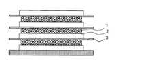
従来の三次元LSIは図1に示すようにそれぞれの基板3上に形成した二次元集積回路層2を接着層1等を介して多段に積み重ねたものであり、このときに二次元集積回路層2から発生する熱は、高熱伝導性の基板3を通して外部に逃がして蓄熱を防いでいた。しかしながら、このような三次元LSIにおいては、二次元集積回路層2どうしを、基板3を貫通する配線(図示省略)で接続する必要があった。そこでその加工性の向上のため、図2のように基板3を薄化することが試みられており、さらには基板3自体を蒸着法(PVD)等により薄膜として形成することも考えられている。このように、高熱伝導性の基板3が薄化あるいは薄膜化した場合、十分な厚みを持たないため、逃がせる熱の量が二次元集積回路層2で発生する熱量よりも少なくなるという課題が起こりつつある。このため、接着層1にも熱を逃がす機能が求められるようになっていた。
ここで接着層1としては加工性の見地から、通常樹脂が用いられており、一般の樹脂はSi等の基板に比して格段に熱伝導度が低い。したがって、接着層1中に充填剤を用いて接着層1の熱伝導度を向上させる技術等が用いられてきたが、基板3の熱伝導性と比較すると充分なものではない場合が多かった。(Embodiment of the present invention)
As shown in FIG. 1, a conventional three-dimensional LSI is formed by stacking two-dimensional integrated circuit layers 2 formed on
Here, a resin is usually used as the
一方、本願発明では、積層面と平行方向の熱伝導性が、積層面と垂直方向の熱伝導性よりも高い接着層1を用いている。したがって、例えば図3に示すように、2層以上の二次元集積回路層2の間に接着層1を形成することにより、効率よく三次元LSIの外部へ熱を逃がすことができるようになる。なお、図3では、図の下方側の二次元集積回路層2のみが基板3と積層されているが、例えば図2のように、他の二次元集積回路層2についても基板3上に形成されていてもよい。また、本発明においては、例えば図3に示すように、二次元集積回路層2及び接着層1を導通する高熱伝導性部材4が形成されていることが、放熱性の面からより好ましい。 On the other hand, in this invention, the
上述したように、本発明においては、接着層1は、水平方向には高熱伝導度を持つが鉛直方向の熱伝導性は通常の樹脂と同等以上の熱伝導度を持つ樹脂、あるいはそのような特性を持つように充填剤を添加した樹脂が好適に使用できる。 As described above, in the present invention, the
本発明の三次元LSIは、放熱性が高く、また薄型化可能であることから、種々の電子機器等に好適に用いることができる。 Since the three-dimensional LSI of the present invention has high heat dissipation and can be thinned, it can be suitably used for various electronic devices.
1:接着層
2:二次元集積回路層
3:基板
4:高熱伝導性部材1: Adhesive layer 2: Two-dimensional integrated circuit layer 3: Substrate 4: High thermal conductivity member
Claims (5)
Translated fromJapanese該接着層の、積層面と平行方向の熱伝導性が、積層面と垂直方向の熱伝導性よりも高い
ことを特徴とする三次元LSI。A first two-dimensional integrated circuit layer, an insulating adhesive layer, and a second two-dimensional integrated circuit layer are provided in this order,
A three-dimensional LSI, wherein the adhesive layer has a higher thermal conductivity in a direction parallel to the laminated surface than a thermal conductivity in a direction perpendicular to the laminated surface.
ことを特徴とする請求項1記載の三次元LSI。2. The three-dimensional LSI according to claim 1, wherein the thermal conductivity in the direction parallel to the laminated surface of the adhesive layer is 1.0 W / m · K or more.
ことを特徴とする請求項1又は請求項2に記載の三次元LSI。The three-dimensional LSI according to claim 1 or 2, wherein the adhesive layer has a thickness of 1 µm or more and 50 µm or less.
ことを特徴とする請求項1〜3のいずれか一項に記載の三次元LSI。2. The high thermal conductivity member that conducts the first two-dimensional integrated circuit layer, the adhesive layer, and the second two-dimensional integrated circuit layer in a direction perpendicular to a stacking surface of each layer. The three-dimensional LSI as described in any one of -3.
ことを特徴とする請求項1〜4のいずれか一項に記載の三次元LSI。The three-dimensional LSI according to any one of claims 1 to 4, wherein the number of two-dimensional integrated circuit layers to be stacked is three or more.
Priority Applications (1)
| Application Number | Priority Date | Filing Date | Title |
|---|---|---|---|
| JP2008194408AJP2010034254A (en) | 2008-07-29 | 2008-07-29 | Three-dimensional large-scale integrated circuit (lsi) |
Applications Claiming Priority (1)
| Application Number | Priority Date | Filing Date | Title |
|---|---|---|---|
| JP2008194408AJP2010034254A (en) | 2008-07-29 | 2008-07-29 | Three-dimensional large-scale integrated circuit (lsi) |
Publications (1)
| Publication Number | Publication Date |
|---|---|
| JP2010034254Atrue JP2010034254A (en) | 2010-02-12 |
Family
ID=41738395
Family Applications (1)
| Application Number | Title | Priority Date | Filing Date |
|---|---|---|---|
| JP2008194408APendingJP2010034254A (en) | 2008-07-29 | 2008-07-29 | Three-dimensional large-scale integrated circuit (lsi) |
Country Status (1)
| Country | Link |
|---|---|
| JP (1) | JP2010034254A (en) |
Cited By (38)
| Publication number | Priority date | Publication date | Assignee | Title |
|---|---|---|---|---|
| JP2012174826A (en)* | 2011-02-21 | 2012-09-10 | Napura:Kk | Electronic device and method of manufacturing the same |
| WO2012133818A1 (en)* | 2011-03-31 | 2012-10-04 | 三菱化学株式会社 | Three-dimensional integrated circuit laminate and interlayer filler material for three-dimensional integrated circuit laminate |
| JP2012216839A (en)* | 2011-03-31 | 2012-11-08 | Mitsubishi Chemicals Corp | Three-dimensional integrated circuit laminate |
| JP2012216838A (en)* | 2011-03-31 | 2012-11-08 | Mitsubishi Chemicals Corp | Three-dimensional integrated circuit laminate |
| JP2012216840A (en)* | 2011-03-31 | 2012-11-08 | Mitsubishi Chemicals Corp | Three-dimensional integrated circuit laminate |
| WO2013014542A1 (en)* | 2011-07-22 | 2013-01-31 | International Business Machines Corporation | A system and method to process horizontally aligned graphite nanofibers in a thermal interface material used in 3d chip stacks |
| US8431048B2 (en) | 2010-07-23 | 2013-04-30 | International Business Machines Corporation | Method and system for alignment of graphite nanofibers for enhanced thermal interface material performance |
| JP2013145840A (en)* | 2012-01-16 | 2013-07-25 | Mitsubishi Chemicals Corp | Application liquid for formation of interlayer packed bed layer of three-dimensional integrated circuit and three-dimensional integrated circuit manufacturing method |
| JP2013222889A (en)* | 2012-04-18 | 2013-10-28 | Mitsubishi Chemicals Corp | Interlayer filler composition for three-dimensional lamination type semiconductor device and coating liquid thereof |
| US20140070393A1 (en)* | 2012-09-13 | 2014-03-13 | International Business Machines Corporation | Horizontally and vertically aligned graphite nanofibers thermal interface material for use in chip stacks |
| JP2014511510A (en)* | 2011-02-28 | 2014-05-15 | ジョンソン・アンド・ジョンソン・ビジョン・ケア・インコーポレイテッド | Method of forming a media substrate for an ophthalmic lens and media substrate for an ophthalmic lens |
| KR20150006227A (en)* | 2013-07-08 | 2015-01-16 | 삼성전기주식회사 | High frequency module |
| US9082744B2 (en) | 2013-07-08 | 2015-07-14 | International Business Machines Corporation | Method for aligning carbon nanotubes containing magnetic nanoparticles in a thermosetting polymer using a magnetic field |
| US9090004B2 (en) | 2013-02-06 | 2015-07-28 | International Business Machines Corporation | Composites comprised of aligned carbon fibers in chain-aligned polymer binder |
| US9096784B2 (en) | 2010-07-23 | 2015-08-04 | International Business Machines Corporation | Method and system for allignment of graphite nanofibers for enhanced thermal interface material performance |
| WO2015186625A1 (en)* | 2014-06-03 | 2015-12-10 | 株式会社日本製鋼所 | Method for producing semiconductor having gettering layer, method for manufacturing semiconductor device, and semiconductor device |
| US9245813B2 (en) | 2013-01-30 | 2016-01-26 | International Business Machines Corporation | Horizontally aligned graphite nanofibers in etched silicon wafer troughs for enhanced thermal performance |
| JP2016178162A (en)* | 2015-03-19 | 2016-10-06 | 株式会社ディスコ | Manufacturing method of laminated device |
| JP2017028169A (en)* | 2015-07-24 | 2017-02-02 | トヨタ自動車株式会社 | Semiconductor device and semiconductor device manufacturing method |
| US9675443B2 (en) | 2009-09-10 | 2017-06-13 | Johnson & Johnson Vision Care, Inc. | Energized ophthalmic lens including stacked integrated components |
| US9698129B2 (en) | 2011-03-18 | 2017-07-04 | Johnson & Johnson Vision Care, Inc. | Stacked integrated component devices with energization |
| US9704793B2 (en) | 2011-01-04 | 2017-07-11 | Napra Co., Ltd. | Substrate for electronic device and electronic device |
| US9804418B2 (en) | 2011-03-21 | 2017-10-31 | Johnson & Johnson Vision Care, Inc. | Methods and apparatus for functional insert with power layer |
| US9889615B2 (en) | 2011-03-18 | 2018-02-13 | Johnson & Johnson Vision Care, Inc. | Stacked integrated component media insert for an ophthalmic device |
| US10345620B2 (en) | 2016-02-18 | 2019-07-09 | Johnson & Johnson Vision Care, Inc. | Methods and apparatus to form biocompatible energization elements incorporating fuel cells for biomedical devices |
| US10361404B2 (en) | 2014-08-21 | 2019-07-23 | Johnson & Johnson Vision Care, Inc. | Anodes for use in biocompatible energization elements |
| US10361405B2 (en) | 2014-08-21 | 2019-07-23 | Johnson & Johnson Vision Care, Inc. | Biomedical energization elements with polymer electrolytes |
| US10367233B2 (en) | 2014-08-21 | 2019-07-30 | Johnson & Johnson Vision Care, Inc. | Biomedical energization elements with polymer electrolytes and cavity structures |
| US10374216B2 (en) | 2014-08-21 | 2019-08-06 | Johnson & Johnson Vision Care, Inc. | Pellet form cathode for use in a biocompatible battery |
| US10381687B2 (en) | 2014-08-21 | 2019-08-13 | Johnson & Johnson Vision Care, Inc. | Methods of forming biocompatible rechargable energization elements for biomedical devices |
| US10386656B2 (en) | 2014-08-21 | 2019-08-20 | Johnson & Johnson Vision Care, Inc. | Methods and apparatus to form separators for biocompatible energization elements for biomedical devices |
| US10451897B2 (en) | 2011-03-18 | 2019-10-22 | Johnson & Johnson Vision Care, Inc. | Components with multiple energization elements for biomedical devices |
| US10558062B2 (en) | 2014-08-21 | 2020-02-11 | Johnson & Johnson Vision Care, Inc. | Methods and apparatus to form biocompatible energization primary elements for biomedical device |
| US10598958B2 (en) | 2014-08-21 | 2020-03-24 | Johnson & Johnson Vision Care, Inc. | Device and methods for sealing and encapsulation for biocompatible energization elements |
| US10627651B2 (en) | 2014-08-21 | 2020-04-21 | Johnson & Johnson Vision Care, Inc. | Methods and apparatus to form biocompatible energization primary elements for biomedical devices with electroless sealing layers |
| CN111108595A (en)* | 2017-09-29 | 2020-05-05 | 长濑化成株式会社 | Method for manufacturing mounting structure and laminated sheet used therein |
| CN111354717A (en)* | 2018-12-21 | 2020-06-30 | 三星电子株式会社 | Monolithic three-dimensional integrated circuit including a heat shield stack and method of manufacturing the same |
| US10775644B2 (en) | 2012-01-26 | 2020-09-15 | Johnson & Johnson Vision Care, Inc. | Ophthalmic lens assembly having an integrated antenna structure |
Citations (4)
| Publication number | Priority date | Publication date | Assignee | Title |
|---|---|---|---|---|
| JPS5890730A (en)* | 1981-11-25 | 1983-05-30 | Mitsubishi Electric Corp | semiconductor equipment |
| JPH06105779B2 (en)* | 1983-02-28 | 1994-12-21 | 双葉電子工業株式会社 | Semiconductor device and manufacturing method thereof |
| JP2005268513A (en)* | 2004-03-18 | 2005-09-29 | Seiko Epson Corp | Electric device and method for manufacturing electric device |
| JP2008518383A (en)* | 2004-10-21 | 2008-05-29 | 松下電器産業株式会社 | Lighting device |
- 2008
- 2008-07-29JPJP2008194408Apatent/JP2010034254A/enactivePending
Patent Citations (4)
| Publication number | Priority date | Publication date | Assignee | Title |
|---|---|---|---|---|
| JPS5890730A (en)* | 1981-11-25 | 1983-05-30 | Mitsubishi Electric Corp | semiconductor equipment |
| JPH06105779B2 (en)* | 1983-02-28 | 1994-12-21 | 双葉電子工業株式会社 | Semiconductor device and manufacturing method thereof |
| JP2005268513A (en)* | 2004-03-18 | 2005-09-29 | Seiko Epson Corp | Electric device and method for manufacturing electric device |
| JP2008518383A (en)* | 2004-10-21 | 2008-05-29 | 松下電器産業株式会社 | Lighting device |
Cited By (55)
| Publication number | Priority date | Publication date | Assignee | Title |
|---|---|---|---|---|
| US9675443B2 (en) | 2009-09-10 | 2017-06-13 | Johnson & Johnson Vision Care, Inc. | Energized ophthalmic lens including stacked integrated components |
| US9096784B2 (en) | 2010-07-23 | 2015-08-04 | International Business Machines Corporation | Method and system for allignment of graphite nanofibers for enhanced thermal interface material performance |
| US8431048B2 (en) | 2010-07-23 | 2013-04-30 | International Business Machines Corporation | Method and system for alignment of graphite nanofibers for enhanced thermal interface material performance |
| US9704793B2 (en) | 2011-01-04 | 2017-07-11 | Napra Co., Ltd. | Substrate for electronic device and electronic device |
| JP2012174826A (en)* | 2011-02-21 | 2012-09-10 | Napura:Kk | Electronic device and method of manufacturing the same |
| US9703120B2 (en) | 2011-02-28 | 2017-07-11 | Johnson & Johnson Vision Care, Inc. | Methods and apparatus for an ophthalmic lens with functional insert layers |
| JP2014511510A (en)* | 2011-02-28 | 2014-05-15 | ジョンソン・アンド・ジョンソン・ビジョン・ケア・インコーポレイテッド | Method of forming a media substrate for an ophthalmic lens and media substrate for an ophthalmic lens |
| US10451897B2 (en) | 2011-03-18 | 2019-10-22 | Johnson & Johnson Vision Care, Inc. | Components with multiple energization elements for biomedical devices |
| US9914273B2 (en) | 2011-03-18 | 2018-03-13 | Johnson & Johnson Vision Care, Inc. | Method for using a stacked integrated component media insert in an ophthalmic device |
| US9889615B2 (en) | 2011-03-18 | 2018-02-13 | Johnson & Johnson Vision Care, Inc. | Stacked integrated component media insert for an ophthalmic device |
| US9698129B2 (en) | 2011-03-18 | 2017-07-04 | Johnson & Johnson Vision Care, Inc. | Stacked integrated component devices with energization |
| US9804418B2 (en) | 2011-03-21 | 2017-10-31 | Johnson & Johnson Vision Care, Inc. | Methods and apparatus for functional insert with power layer |
| TWI575692B (en)* | 2011-03-31 | 2017-03-21 | Mitsubishi Chem Corp | Three - dimensional volume of the product body |
| US9508648B2 (en) | 2011-03-31 | 2016-11-29 | Mitsubishi Chemical Corporation | Three-dimensional integrated circuit laminate, and interlayer filler for three-dimensional integrated circuit laminate |
| JP2012216840A (en)* | 2011-03-31 | 2012-11-08 | Mitsubishi Chemicals Corp | Three-dimensional integrated circuit laminate |
| KR20140007429A (en)* | 2011-03-31 | 2014-01-17 | 미쓰비시 가가꾸 가부시키가이샤 | Three-dimensional integrated circuit laminate and interlayer filler material for three-dimensional integrated circuit laminate |
| JP2012216838A (en)* | 2011-03-31 | 2012-11-08 | Mitsubishi Chemicals Corp | Three-dimensional integrated circuit laminate |
| CN103443919A (en)* | 2011-03-31 | 2013-12-11 | 三菱化学株式会社 | Three-dimensional integrated circuit laminate, and interlayer filling material for three-dimensional integrated circuit laminate |
| JP2012216839A (en)* | 2011-03-31 | 2012-11-08 | Mitsubishi Chemicals Corp | Three-dimensional integrated circuit laminate |
| WO2012133818A1 (en)* | 2011-03-31 | 2012-10-04 | 三菱化学株式会社 | Three-dimensional integrated circuit laminate and interlayer filler material for three-dimensional integrated circuit laminate |
| US9847298B2 (en) | 2011-03-31 | 2017-12-19 | Mitsubishi Chemical Corporation | Three-dimensional integrated circuit laminate, and interlayer filler for three-dimensional integrated circuit laminate |
| GB2506534B (en)* | 2011-07-22 | 2015-05-06 | Ibm | A system and method to process horizontally aligned graphite nanofibers in a thermal interface material used in 3d chip stacks |
| US9257359B2 (en) | 2011-07-22 | 2016-02-09 | International Business Machines Corporation | System and method to process horizontally aligned graphite nanofibers in a thermal interface material used in 3D chip stacks |
| GB2506534A (en)* | 2011-07-22 | 2014-04-02 | Ibm | A system and method to process horizontally aligned graphite nanofibers in a thermal interface material used in 3d chip stacks |
| WO2013014542A1 (en)* | 2011-07-22 | 2013-01-31 | International Business Machines Corporation | A system and method to process horizontally aligned graphite nanofibers in a thermal interface material used in 3d chip stacks |
| JP2013145840A (en)* | 2012-01-16 | 2013-07-25 | Mitsubishi Chemicals Corp | Application liquid for formation of interlayer packed bed layer of three-dimensional integrated circuit and three-dimensional integrated circuit manufacturing method |
| US10775644B2 (en) | 2012-01-26 | 2020-09-15 | Johnson & Johnson Vision Care, Inc. | Ophthalmic lens assembly having an integrated antenna structure |
| JP2013222889A (en)* | 2012-04-18 | 2013-10-28 | Mitsubishi Chemicals Corp | Interlayer filler composition for three-dimensional lamination type semiconductor device and coating liquid thereof |
| US9111899B2 (en)* | 2012-09-13 | 2015-08-18 | Lenovo | Horizontally and vertically aligned graphite nanofibers thermal interface material for use in chip stacks |
| CN103681517A (en)* | 2012-09-13 | 2014-03-26 | 国际商业机器公司 | Thermal interface material for use in chip stacks |
| US20140070393A1 (en)* | 2012-09-13 | 2014-03-13 | International Business Machines Corporation | Horizontally and vertically aligned graphite nanofibers thermal interface material for use in chip stacks |
| US9245813B2 (en) | 2013-01-30 | 2016-01-26 | International Business Machines Corporation | Horizontally aligned graphite nanofibers in etched silicon wafer troughs for enhanced thermal performance |
| US9090004B2 (en) | 2013-02-06 | 2015-07-28 | International Business Machines Corporation | Composites comprised of aligned carbon fibers in chain-aligned polymer binder |
| KR102041639B1 (en)* | 2013-07-08 | 2019-11-07 | 삼성전기주식회사 | High frequency module |
| US9406651B2 (en) | 2013-07-08 | 2016-08-02 | Globalfoundries Inc. | Chip stack with oleic acid-aligned nanotubes in thermal interface material |
| US9082744B2 (en) | 2013-07-08 | 2015-07-14 | International Business Machines Corporation | Method for aligning carbon nanotubes containing magnetic nanoparticles in a thermosetting polymer using a magnetic field |
| KR20150006227A (en)* | 2013-07-08 | 2015-01-16 | 삼성전기주식회사 | High frequency module |
| JPWO2015186625A1 (en)* | 2014-06-03 | 2017-06-22 | 株式会社日本製鋼所 | Manufacturing method of semiconductor having gettering layer, manufacturing method of semiconductor device, and semiconductor device |
| WO2015186625A1 (en)* | 2014-06-03 | 2015-12-10 | 株式会社日本製鋼所 | Method for producing semiconductor having gettering layer, method for manufacturing semiconductor device, and semiconductor device |
| US10361405B2 (en) | 2014-08-21 | 2019-07-23 | Johnson & Johnson Vision Care, Inc. | Biomedical energization elements with polymer electrolytes |
| US10627651B2 (en) | 2014-08-21 | 2020-04-21 | Johnson & Johnson Vision Care, Inc. | Methods and apparatus to form biocompatible energization primary elements for biomedical devices with electroless sealing layers |
| US10367233B2 (en) | 2014-08-21 | 2019-07-30 | Johnson & Johnson Vision Care, Inc. | Biomedical energization elements with polymer electrolytes and cavity structures |
| US10374216B2 (en) | 2014-08-21 | 2019-08-06 | Johnson & Johnson Vision Care, Inc. | Pellet form cathode for use in a biocompatible battery |
| US10381687B2 (en) | 2014-08-21 | 2019-08-13 | Johnson & Johnson Vision Care, Inc. | Methods of forming biocompatible rechargable energization elements for biomedical devices |
| US10386656B2 (en) | 2014-08-21 | 2019-08-20 | Johnson & Johnson Vision Care, Inc. | Methods and apparatus to form separators for biocompatible energization elements for biomedical devices |
| US10361404B2 (en) | 2014-08-21 | 2019-07-23 | Johnson & Johnson Vision Care, Inc. | Anodes for use in biocompatible energization elements |
| US10598958B2 (en) | 2014-08-21 | 2020-03-24 | Johnson & Johnson Vision Care, Inc. | Device and methods for sealing and encapsulation for biocompatible energization elements |
| US10558062B2 (en) | 2014-08-21 | 2020-02-11 | Johnson & Johnson Vision Care, Inc. | Methods and apparatus to form biocompatible energization primary elements for biomedical device |
| JP2016178162A (en)* | 2015-03-19 | 2016-10-06 | 株式会社ディスコ | Manufacturing method of laminated device |
| JP2017028169A (en)* | 2015-07-24 | 2017-02-02 | トヨタ自動車株式会社 | Semiconductor device and semiconductor device manufacturing method |
| US10345620B2 (en) | 2016-02-18 | 2019-07-09 | Johnson & Johnson Vision Care, Inc. | Methods and apparatus to form biocompatible energization elements incorporating fuel cells for biomedical devices |
| CN111108595A (en)* | 2017-09-29 | 2020-05-05 | 长濑化成株式会社 | Method for manufacturing mounting structure and laminated sheet used therein |
| US11799442B2 (en) | 2017-09-29 | 2023-10-24 | Nagase Chemtex Corporation | Manufacturing method of mounting structure, and laminate sheet therefor |
| CN111354717A (en)* | 2018-12-21 | 2020-06-30 | 三星电子株式会社 | Monolithic three-dimensional integrated circuit including a heat shield stack and method of manufacturing the same |
| CN111354717B (en)* | 2018-12-21 | 2024-08-02 | 三星电子株式会社 | Monolithic three-dimensional integrated circuit including a stack of heat shields and method of manufacturing the same |
Similar Documents
| Publication | Publication Date | Title |
|---|---|---|
| JP2010034254A (en) | Three-dimensional large-scale integrated circuit (lsi) | |
| US9961809B1 (en) | Heat radiation sheet and method for manufacturing of the same | |
| CN101939396B (en) | Adhesive composition for electronic components and adhesive sheet for electronic components using the same | |
| CN106463496B (en) | Integrated devices including high density interconnects in inorganic layers and redistribution layers in organic layers | |
| US6660566B2 (en) | Heat conductive molded body and manufacturing method thereof and semiconductor device | |
| TW202315044A (en) | Microelectronic assemblies having a hybrid bonded interposer for die-to-die fan-out scaling | |
| KR101009103B1 (en) | Double-sided electrode package and its manufacturing method | |
| JP6023474B2 (en) | Thermally conductive insulating sheet, metal base substrate and circuit board, and manufacturing method thereof | |
| TWI835762B (en) | Laminated bodies and electronic devices | |
| US9240394B1 (en) | Stacked chips attached to heat sink having bonding pads | |
| US12199018B2 (en) | Direct bonding in microelectronic assemblies | |
| US11407201B2 (en) | Composite member | |
| TWI886336B (en) | Hermetic sealing structures in microelectronic assemblies having direct bonding | |
| TW201131669A (en) | Manufacturing method for semiconductor device | |
| JP2009194359A (en) | Adhesive film for circuit connection, and connection structure of circuit member and method of connecting circuit member using the same | |
| US11276634B2 (en) | High density package substrate formed with dielectric bi-layer | |
| JP2012253167A (en) | Thermally conductive insulation sheet, metal base substrate and circuit board | |
| JP2016192474A (en) | Granulated powder, resin composition for heat dissipation, heat dissipation sheet, heat dissipation member, and semiconductor device | |
| JP7007161B2 (en) | Resin composition and laminate | |
| TW201904765A (en) | Heat dissipation sheet, method for manufacturing heat dissipation sheet, and laminated body | |
| US20240084172A1 (en) | Adhesive composition, film adhesive, and semiconductor package using film adhesive and producing method thereof | |
| KR102565178B1 (en) | Soft-rigid-soft multi layer Thermal InterFace material, preparing method of the same, and heat radiating system including the same | |
| CN110612603A (en) | Insulating sheet and laminate | |
| JP6276576B2 (en) | Thermally conductive sheet for semiconductor modules | |
| JP7129554B2 (en) | Laminate manufacturing method and functional sheet manufacturing method |
Legal Events
| Date | Code | Title | Description |
|---|---|---|---|
| A621 | Written request for application examination | Free format text:JAPANESE INTERMEDIATE CODE: A621 Effective date:20110531 | |
| A131 | Notification of reasons for refusal | Free format text:JAPANESE INTERMEDIATE CODE: A131 Effective date:20130416 | |
| A131 | Notification of reasons for refusal | Free format text:JAPANESE INTERMEDIATE CODE: A131 Effective date:20140121 | |
| A521 | Request for written amendment filed | Free format text:JAPANESE INTERMEDIATE CODE: A523 Effective date:20140324 | |
| A02 | Decision of refusal | Free format text:JAPANESE INTERMEDIATE CODE: A02 Effective date:20141007 |