JP2010032545A - Apparatus for measuring optical displacement - Google Patents
Apparatus for measuring optical displacementDownload PDFInfo
- Publication number
- JP2010032545A JP2010032545AJP2009256267AJP2009256267AJP2010032545AJP 2010032545 AJP2010032545 AJP 2010032545AJP 2009256267 AJP2009256267 AJP 2009256267AJP 2009256267 AJP2009256267 AJP 2009256267AJP 2010032545 AJP2010032545 AJP 2010032545A
- Authority
- JP
- Japan
- Prior art keywords
- scale
- receiving element
- light
- substrate
- element array
- Prior art date
- Legal status (The legal status is an assumption and is not a legal conclusion. Google has not performed a legal analysis and makes no representation as to the accuracy of the status listed.)
- Granted
Links
- 238000006073displacement reactionMethods0.000titleclaimsabstractdescription63
- 230000003287optical effectEffects0.000titleclaimsabstractdescription54
- 239000000758substrateSubstances0.000claimsabstractdescription71
- 239000004065semiconductorSubstances0.000claimsabstractdescription19
- 239000011347resinSubstances0.000claimsdescription22
- 229920005989resinPolymers0.000claimsdescription22
- 238000000059patterningMethods0.000claimsdescription5
- 238000003491arrayMethods0.000description16
- 239000010410layerSubstances0.000description10
- 101100243945Fusarium vanettenii PDAT9 geneProteins0.000description5
- 208000012204PDA1Diseases0.000description5
- 101150102492pda1 geneProteins0.000description5
- 101001072191Homo sapiens Protein disulfide-isomerase A2Proteins0.000description4
- 102100036351Protein disulfide-isomerase A2Human genes0.000description4
- 239000000463materialSubstances0.000description4
- 208000030825patent ductus arteriosus 2Diseases0.000description4
- 208000030770patent ductus arteriosus 3Diseases0.000description4
- 238000001459lithographyMethods0.000description3
- 230000002093peripheral effectEffects0.000description3
- VYPSYNLAJGMNEJ-UHFFFAOYSA-NSilicium dioxideChemical compoundO=[Si]=OVYPSYNLAJGMNEJ-UHFFFAOYSA-N0.000description2
- 238000001514detection methodMethods0.000description2
- 239000011521glassSubstances0.000description2
- 239000011229interlayerSubstances0.000description2
- 238000005259measurementMethods0.000description2
- 239000002184metalSubstances0.000description2
- 238000012986modificationMethods0.000description2
- 230000004048modificationEffects0.000description2
- 229910052814silicon oxideInorganic materials0.000description2
- 101100123718Neurospora crassa (strain ATCC 24698 / 74-OR23-1A / CBS 708.71 / DSM 1257 / FGSC 987) pda-1 geneProteins0.000description1
- 230000015572biosynthetic processEffects0.000description1
- UHYPYGJEEGLRJD-UHFFFAOYSA-Ncadmium(2+);selenium(2-)Chemical compound[Se-2].[Cd+2]UHYPYGJEEGLRJD-UHFFFAOYSA-N0.000description1
- 230000008021depositionEffects0.000description1
- 238000004519manufacturing processMethods0.000description1
- 229920001721polyimidePolymers0.000description1
- 239000009719polyimide resinSubstances0.000description1
- SBIBMFFZSBJNJF-UHFFFAOYSA-Nselenium;zincChemical compound[Se]=[Zn]SBIBMFFZSBJNJF-UHFFFAOYSA-N0.000description1
- 229910052710siliconInorganic materials0.000description1
- 239000010703siliconSubstances0.000description1
Images


Landscapes
- Optical Transform (AREA)
Abstract
Description
Translated fromJapaneseこの発明は、光学式変位測定装置に関する。 The present invention relates to an optical displacement measuring device.
従来より、x軸及びy軸の二軸方向の変位を光学的に検出するためのxyスケールが知られている。このxyスケールに対してセンサヘッドには、x軸及びy軸方向の変位信号を出力する二つの受光デバイスが搭載される。 Conventionally, an xy scale for optically detecting a biaxial displacement of the x-axis and the y-axis is known. Two light receiving devices that output displacement signals in the x-axis and y-axis directions are mounted on the sensor head with respect to the xy scale.
しかし、二つの受光デバイスを基板に搭載した場合、xy直角度は取り付け精度に依存するため、高精度のxy直角度を得ることが難しい。また、二つの受光デバイスは基板の別々の領域に搭載されることになるため、センサヘッドの小型化ができない。また通常、受光デバイスを搭載する基板にはガラス基板等のリジッドな平坦基板が用いられる。しかし、xyスケールのスケール面は、平面とは限られず、球面や円筒面等の場合もある。このため、リジッドな基板に受光デバイスを搭載する構造では、種々のスケール面を持つxyスケールに柔軟に対応させることができない。 However, when two light receiving devices are mounted on a substrate, it is difficult to obtain a highly accurate xy squareness because the xy squareness depends on the mounting accuracy. Further, since the two light receiving devices are mounted in different regions of the substrate, the sensor head cannot be reduced in size. Usually, a rigid flat substrate such as a glass substrate is used as the substrate on which the light receiving device is mounted. However, the scale surface of the xy scale is not limited to a flat surface, and may be a spherical surface or a cylindrical surface. For this reason, the structure in which the light receiving device is mounted on a rigid substrate cannot flexibly cope with an xy scale having various scale surfaces.
この発明は、上記事情を考慮してなされたもので、二軸変位検出用の受光素子アレイを優れた直角度をもって一体化した光学式変位測定装置を提供することを目的としている。 この発明はまた、二軸変位検出用の受光素子アレイを小型に集積したセンサヘッドを持つ光学式変位測定装置を提供することを目的とする。この発明は更に、種々のスケール面を柔軟に対応できるセンサヘッドを持つ光学式変位測定装置を提供することを目的とする。 The present invention has been made in view of the above circumstances, and an object thereof is to provide an optical displacement measuring device in which a light receiving element array for detecting biaxial displacement is integrated with an excellent squareness. Another object of the present invention is to provide an optical displacement measuring device having a sensor head in which a light receiving element array for detecting biaxial displacement is integrated in a small size. Another object of the present invention is to provide an optical displacement measuring device having a sensor head that can flexibly handle various scale surfaces.
この発明に係る光学式変位測定装置は、二軸方向に光学格子が形成されたスケールと、このスケールに対向して二軸方向に相対移動可能に配置されて相対移動を光学的に検出して変位信号を出力する受光素子アレイを有するセンサヘッドとを備え、前記センサヘッドの受光素子アレイは、基板と、この基板上に堆積された半導体膜により形成された、前記光学格子の第1軸方向に所定ピッチで配列されて第1軸方向の変位に対応する変位信号を出力する第1の受光素子群と、この第1の受光素子群を覆って形成された絶縁層と、この絶縁層上に堆積された半導体膜により形成された、前記光学格子の第2軸方向に所定ピッチで配列されて第2軸方向の変位に対応する変位信号を出力する第2の受光素子群とを有することを特徴とする。 An optical displacement measuring apparatus according to the present invention is arranged so that a scale having an optical grating formed in a biaxial direction and a relative movement in a biaxial direction facing the scale and optically detecting the relative movement. A sensor head having a light receiving element array for outputting a displacement signal, and the light receiving element array of the sensor head is formed of a substrate and a semiconductor film deposited on the substrate, and is in a first axial direction of the optical grating. A first light receiving element group that outputs a displacement signal corresponding to the displacement in the first axial direction, and an insulating layer formed to cover the first light receiving element group, and on the insulating layer And a second light receiving element group arranged at a predetermined pitch in the second axis direction of the optical grating and outputting a displacement signal corresponding to the displacement in the second axis direction. It is characterized by.
この発明によると、二軸方向の変位測定を行う受光素子アレイは、半導体膜の膜堆積とリソグラフィにより作られる受光素子群の積層構造として構成される。従って二軸の受光素子群の直角度が優れたものとなり、小型で高性能の光学式変位測定装置が得られる。 According to the present invention, the light receiving element array for measuring the displacement in the biaxial direction is configured as a stacked structure of light receiving element groups formed by film deposition of a semiconductor film and lithography. Accordingly, the perpendicularity of the biaxial light receiving element group becomes excellent, and a small and high performance optical displacement measuring device can be obtained.
この発明において、受光素子アレイの基板は例えば、第1及び第2の受光素子群が積層された面と反対側の面を光入射面とする透明基板が用いられる。またこの基板として、フレキシブル樹脂基板を用いることができる。これにより、二次元的な光学格子を持つスケール面が曲面の場合にも、柔軟に対向させることができる。 In the present invention, the substrate of the light receiving element array is, for example, a transparent substrate having a light incident surface on a surface opposite to the surface on which the first and second light receiving element groups are stacked. A flexible resin substrate can be used as this substrate. Thereby, even when the scale surface having a two-dimensional optical grating is a curved surface, it can be flexibly opposed.
この発明に係る光学式変位測定装置はまた、光学格子が形成されたスケールと、このスケールに対向して相対移動可能に配置されて相対移動を光学的に検出して変位信号を出力する受光素子アレイを有するセンサヘッドとを備え、前記受光素子アレイは、基板上に堆積された半導体膜をパターニングして得られる受光素子群を有し且つ、前記スケール及び受光素子アレイの少なくとも一方がフレキシブル樹脂基板に形成されていることを特徴とする。 The optical displacement measuring apparatus according to the present invention also includes a scale on which an optical grating is formed, and a light receiving element that is disposed so as to be relatively movable so as to face the scale and optically detects the relative movement and outputs a displacement signal. A sensor head having an array, the light receiving element array having a light receiving element group obtained by patterning a semiconductor film deposited on the substrate, and at least one of the scale and the light receiving element array being a flexible resin substrate It is characterized by being formed.
この発明によると、スケールと受光素子アレイの少なくとも一方をフレキシブル樹脂基板に形成することによって、スケールの光学格子が一次元又は二次元のいずれであっても、スケール面形状が円筒面、球面、自由曲面等の場合に柔軟に対応させることができる。具体的にこの発明において、好ましくは、受光素子アレイが、フレキシブル樹脂基板と、このフレキシブル樹脂基板上に堆積された半導体膜により形成されて異なる位相の変位信号を出力する複数の受光素子とを備えて構成される。スケールが二次元の光学格子を有する場合に、受光素子アレイは、二次元の光学格子に対応して基板の異なる位置に形成された第1及び第2の受光素子群を有するものとして構成しいてもよいし、或いは二次元の光学格子に対応して基板の同じ位置に絶縁層を介して積層形成された第1及び第2の受光素子群を有するものとして構成することもできる。 According to the present invention, by forming at least one of the scale and the light receiving element array on the flexible resin substrate, the scale surface shape can be a cylindrical surface, a spherical surface, a free surface, regardless of whether the optical grating of the scale is one-dimensional or two-dimensional. It is possible to flexibly cope with a curved surface or the like. Specifically, in the present invention, preferably, the light receiving element array includes a flexible resin substrate and a plurality of light receiving elements that are formed of a semiconductor film deposited on the flexible resin substrate and output displacement signals having different phases. Configured. When the scale has a two-dimensional optical grating, the light-receiving element array is configured to have first and second light-receiving element groups formed at different positions on the substrate corresponding to the two-dimensional optical grating. Alternatively, it may be configured to have a first and a second light receiving element group formed in a laminated manner via an insulating layer at the same position of the substrate corresponding to a two-dimensional optical grating.
この発明によれば、二軸変位検出用の受光素子アレイを優れた直角度をもって一体化した小型の光学式変位測定装置が得られる。またこの発明によれば、種々のスケール面を柔軟に対応できるセンサヘッドを持つ光学式変位測定装置が得られる。 According to the present invention, it is possible to obtain a small optical displacement measuring device in which a light receiving element array for detecting biaxial displacement is integrated with an excellent squareness. According to the present invention, an optical displacement measuring device having a sensor head that can flexibly handle various scale surfaces can be obtained.
以下、図面を参照して、この発明の実施例を説明する。図1は、この発明の光学式エンコーダの基本構成を示す斜視図である。スケール1は、x軸及びy軸の直交二軸方向の二次元光学格子11が形成されたxyスケールである。センサヘッド2は、スケール1に対向して二軸方向に相対移動可能に配置される。センサヘッド2には、二軸方向の相対移動を光学的に検出して各軸の変位信号を出力する受光素子アレイ3と、スケール1を照射するLED等の光源4を有する。 Embodiments of the present invention will be described below with reference to the drawings. FIG. 1 is a perspective view showing the basic configuration of the optical encoder of the present invention. The
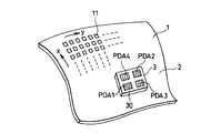
受光素子アレイ3は、x軸方向の変位を検出するためのフォトダイオードアレイPDA1,PDA2と、y軸方向変位を検出するためのフォトダイオードアレイPDA3,PDA4とを有する。具体的に例えば、フォトダイオードアレイPDA1には、A相出力用とこれとは90°位相がずれたB相出力用のフォトダイオード(PD)群が所定ピッチで配列され、フォトダイオードアレイPDA2には、A,B相出力に対してそれぞれ逆相のAB相及びBB相出力用のフォトダイオード(PD)群が所定ピッチで配列される。同様に、フォトダイオードアレイPDA3には、A相及びB相出力用のフォトダイオード(PD)群が配列され、フォトダイオードアレイPDA4には、AB相及びBB相出力用のフォトダイオード(PD)群が配列される。 The light
この発明において、これらの二軸方向のフォトダイオードアレイPDA1−PDA4を含む受光素子アレイ3は、所定のアレイ基板30上に堆積されたアモルファス半導体膜のパターニングにより一体的に作られている。図2は、この受光素子アレイ3のレイアウトを示し、図3は図2のA−A’断面構造を示している。基板30は透明基板であり、この例では基板30の裏面がスケールからの反射光が入る光入射面となる。 In the present invention, the light receiving
基板30上には、各フォトダイオードPDの共通電極となる透明電極31が形成されている。この透明電極31上に堆積されたアモルファス半導体膜32をパターニングすることにより、x軸方向に細長いストライプ状のフォトダイオードPDからなるアレイPDA3,PDA4と、y軸方向に細長いストライプ状のフォトダイオードPDからなるアレイPDA1,PDA2が同時に形成されている。 A
半導体膜32は具体的には、pin層構造又はpn層構造を有する。各フォトダイオードPDの上面には端子電極33が形成されている。この端子電極33は、半導体膜32と連続的に堆積され、半導体膜32と同時にパターニングされる。各フォトダイオードPDはシリコン酸化膜等の絶縁層34で覆われる。 Specifically, the
この様に、xyスケール1の二軸方向の変位検出を行うフォトダイオードアレイPDA1,PDA2とPDA3,PDA4を共通のアモルファス半導体膜32のパターニングにより一体に形成することによって、これらを個別に作って基板に取り付ける場合に比べて、xy二軸の直角度は優れたものとなり、また全体として受光素子アレイ3が小型になる。 In this manner, the photodiode arrays PDA1, PDA2 and PDA3, PDA4 for detecting displacement in the biaxial direction of the
図1−図3の構成によるセンサヘッド2は、x軸及びy軸方向の直線変位測定のみならず、4つのフォトダイオードアレイPDA1−PDA4の変位信号の処理により、xy平面内のセンサヘッド2とスケール1の間の相対回転角変位θの測定も可能である。 The
なお、図1−図3の構成において、アモルファス半導体膜32としては、代表的にはシリコンが用いられるが、その他ZnSe,CdSe等が用いられる。以下の例においても同様である。 1 to 3, silicon is typically used as the
図1〜図3の構成を基本として、二軸方向のフォトダイオードアレイを積層構造とする例を次に説明する。図4はそのような受光素子アレイ3のレイアウトであり、図5及び図6はそれぞれ、図3のA−A’及びB−B’断面図である。y軸方向の変位検出用フォトダイオードアレイPDAyと、x軸方向の変位検出用フォトダイオードアレイPDAxとは、異なるアモルファス半導体膜32,36を用いて形成される。透明基板30上に、フォトダイオードアレイPDAyの共通電極となる透明電極31を介して第1層アモルファス半導体膜32が堆積され、これをパターニングしてフォトダイオードアレイPDAyが形成される。 Next, an example in which the biaxial photodiode array has a laminated structure based on the configuration of FIGS. FIG. 4 is a layout of such a light receiving
フォトダイオードアレイPDAyの各端子電極33は透明電極とする。このフォトダイオードアレイPDAyはシリコン酸化膜等の層間絶縁膜34で覆われる。この層間絶縁膜34上に、フォトダイオードアレイPDAxの共通電極となる透明電極35を介して第2層アモルファス半導体膜36が堆積され、これをパターニングしてフォトダイオードアレイPDAxが形成される。フォトダイオードアレイPDAxの各端子電極37は金属電極を用いうる。フォトダイオードアレイPDAxは更に絶縁層37により覆われる。 Each
なお、フォトダイオードアレイPDAyの端子電極33を金属電極とすることもできる。この場合、端子電極33により、基板裏面からのフォトダイオードアレイPDAxへの光が遮られるが、これはフォトダイオードアレイPDAx,PDAyの面積比率を調整して、両者にほぼ同等の光量が入るようにすれば、問題ない。また、面積比率とは別に、或いは面積比率と共に、フォトダイオードアレイPDAx,PDAyの出力利得を調整することによっても、対処することができる。 Note that the
この様に、二軸方向の変位検出用のフォトダイオードアレイを積層することにより、受光素子アレイ3は一層小型になる。また、フォトダイオードアレイの積層は、リソグラフィ技術により行われるので、xy二軸の直角度も優れたものとなる。下部フォトダイオードアレイPDAyは、上下電極とも透明電極としている。従って、基板30の裏面から入射する光は、フォトダイオードアレイPDAyで一部光電変換される他、上部フォトダイオードアレイPDAxまで透過する。これにより、フォトダイオードアレイPDAy,PDAxともに十分なS/Nの変位信号を得ることができる。 In this manner, the light receiving
以上の構成例において、透明基板30としてガラス基板等の固い基板を用いることもできるが、好ましくはフレキシブル樹脂基板を用いる。フレキシブル樹脂基板としては例えば、ポリイミド樹脂が用いられる。これにより、光学式エンコーダの適用範囲は広いものとなる。その様な応用例を以下に説明する。 In the above configuration example, a hard substrate such as a glass substrate can be used as the
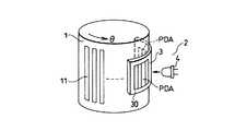
図7は、スケール1が円筒スケールの例である。円筒スケール1にはその外周面に、円筒軸方向(x軸)及び周方向(θ)の二軸の光学格子が形成されている。これに対して、x軸及びθ方向の変位検出を行うフォトダイオードアレイPDA,PDAを形成した受光素子アレイ3の基板30には、フレキシブル樹脂基板を用いている。 FIG. 7 shows an example in which the
受光素子アレイ3は、基板材料の点を除き、図1〜図3と同様のフォトダイオードアレイ構成(或いは図4〜図6と同様のフォトダイオードアレイ構成)を有するものとする。またその製造工程は、基板30が平坦な状態で、膜形成とリソグラフィ技術を利用して実行される。基板30がフレキシブル樹脂基板であれば、得られた受光素子アレイ3を、図7に示すように円筒スケール1の径に応じて湾曲させて、円筒スケール1の外周面に所定ギャップで対向させることができる。 The light
なお、受光素子アレイ3のθ方向のピッチは、湾曲させることにより、平面上でパターン形成した状態のフォトダイオードアレイPDA,PDAのピッチに対して僅かにずれる。しかしこのピッチのずれは、円筒スケール1の径がある程度以上であれば無視できる。従って、フレキシブル樹脂基板を用いることにより、受光素子アレイを実際に適用できる範囲は広いものとなる。なお、上述のピッチのずれは湾曲の径に対応して予測できるから、湾曲を見込んで平面上のパターンピッチを決定することもできる。 Note that the pitch in the θ direction of the light
図8は、スケール1が円筒スケールであるが、測定するのは周方向(θ)方向の一軸のみの例である。即ちスケール1の光学格子11は、外周面にθ方向のみに所定ピッチで形成されている。この場合、受光素子アレイ3も、θ方向のみのフォトダイオードアレイPDAにより構成される。そしてこの場合も基板30としてフレキシブル樹脂基板を用いることにより、図7の場合と同様に、柔軟な適用が可能となる。 FIG. 8 shows an example in which the
図9は、スケール1が自由曲面スケールの例である。自由曲面スケール1にはその自由曲面に、x軸方向及びy軸方向の二軸の光学格子が形成されている。これに対して、x軸方向及びy軸方向の変位検出を行うフォトダイオードアレイPDA,PDAを形成した受光素子アレイ3の基板30には、フレキシブル樹脂基板を用いている。受光素子アレイ3は、基板材料の点を除き、図1〜図3と同様のフォトダイオードアレイ構成(或いは図4〜図6と同様のフォトダイオードアレイ構成)を有するものとする。これにより受光素子アレイ3を、自由曲面スケール1に倣って変形させながら、スケール1の外周面に所定ギャップで対向させることにより、xy軸方向の直線変位及び回転変位θの測定ができる。 FIG. 9 shows an example in which the
なお、図9の構成において、スケール1をフレキシブル基板に形成し、受光素子アレイ3のアレイ基板30をリジッドなものとすることもできる。この場合、スケール1は自由曲面を有する対象物に貼り合わされて自由曲面スケール1となる。これに対してセンサヘッド2を所定ギャップで対向させて相対移動可能とする。図7及び図8の例においても、スケール1の光学格子11をフレキシブル樹脂基板を用いて形成し、これを円筒面に貼り付けることができる。更に、スケール1と受光素子アレイ3のアレイ基板30の双方共に、フレキシブル基板とすることもできる。また受光素子アレイ3にフレキシブル基板を用いた場合には、光源として面発光型の発光素子、例えばフレキシブルに変形可能な有機EL素子を貼り付けて使用することができる。 In the configuration of FIG. 9, the
図10は、スケール1が球面スケールの例である。スケール1はその球面に直交する二つの周方向θ,φの光学格子11が形成されている。このスケール1にキャップを被せるようにセンサヘッド2が取り付けられる。θ方向及びφ方向の変位検出を行うフォトダイオードアレイPDA,PDAを形成した受光素子アレイ3の基板30には、フレキシブル樹脂基板を用いて、スケール1の球面に対向して配置されるようにしている。受光素子アレイ3は、基板材料の点を除き、図1〜図3と同様のフォトダイオードアレイ構成(或いは図4〜図6と同様のフォトダイオードアレイ構成)を有するものとする。このように、受光素子アレイ3の基板をフレキシブル樹脂基板とすることにより、球面スケールにも対応させることができる。 FIG. 10 shows an example in which the
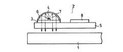
この発明による光学式変位測定装置のセンサヘッド2の具体的な構成例を、以下にいくつか挙げる。図11のセンサヘッド2は、透明基板5を用いて、これに受光素子アレイ3を搭載している。そして受光素子アレイ3上に光源4としてのLEDチップをその上面を発光面として搭載し、このLED搭載部を凸面をなす透明樹脂6でモールドしている。透明樹脂6の凸面には反射膜7を形成している。これにより、LEDからの光は、凸面で反射されてほぼ平行光となり透明基板5を介してスケール1に照射される。この場合、光源光は、受光素子アレイ3の受光素子の形成されていない領域を通って、スケールに照射されるようにする。またこの領域に第1光学格子を形成すれば、3格子システムが構成可能である。また、受光素子アレイ3の下に第1光学格子を備え、光源光が受光素子アレイ3と第1光学格子を通ってスケールに照射されるようにしても、3格子システムが構成可能である。なお図11においては、透明基板5の上に、受光素子アレイ3の出力信号を処理する信号処理回路8も搭載されている。 Some specific examples of the configuration of the
図12は、3格子システムを構成した例である。この場合のセンサヘッド2は、透明基板からなるインデックス基板9の上に、光源側インデックス格子10が形成され、光源4からの光はこのインデックス格子10を介してスケール1に照射されるようにしている。インデックス基板9上にインデックス格子10とは離れて、受光素子アレイ3が搭載されている。 FIG. 12 shows an example in which a three-grid system is configured. In this case, the
図13のセンサヘッド2は、光源4として面発光型LEDを用いた例である。面発光型LEDをその発光面をスケール1側に向けて配置し、その発光面に受光素子アレイ3を搭載している。LEDからの光は、受光素子アレイ3を通してスケール1にほぼ垂直に照射され、スケール1からほぼ垂直に反射される光が受光素子アレイ3により検出されるようにしている。面発光型の発光素子として、LEDの他、例えば有機EL素子を用いることもできる。 The
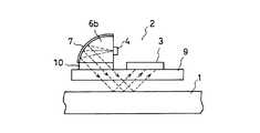
図14は、図11の変形例である。光源は単純に、LED4を配置して構成される。LED4の光は、ほぼ垂直に第1格子と第3格子を兼ねる受光素子アレイ3に入射され、受光素子アレイ3を透過してスケール1に照射される。図15は、図12の変形例である。球体を略1/4分割した形の透明樹脂体6bと反射膜7により凹面鏡を構成し、LED4は発光面を垂直にして透明樹脂体6bの側面に取り付ける。反射膜7で反射された光は、インデックス格子10に斜め入射し、スケール1を照射する。なお、光源側にスケール格子と同じピッチのインデックス格子(又はピンホールアレイ)を用いる3格子システムは、光学的2分割となる(即ち、出力信号ピッチが2格子システムの場合の1/2になる)利点を持つが、光源側のインデックス格子(又はピンポールアレイ)は必ずしも必要ではなく、例えば図12及び図15の構成において、光源側インデックス格子10は省略することもできる。 FIG. 14 is a modification of FIG. The light source is simply configured by arranging the
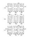
ここまでの例では、受光素子アレイ3の各フォトダイオードPDは細長い矩形パターンとしたが、このフォトダイオードPDのパターンについては、同相のものを複数本束ねた、図16(a)〜(c)に示すようなパターンとすることができる。図16(a)では、複数本のフォトダイオードPDの中央部に、端子配線のコンタクト部となる連結部141を設けている。図16(b)では、複数本のフォトダイオードの端部に連結部142を設けている。また図16(c)では、複数の連結部143を設けている。 In the examples so far, each photodiode PD of the light
1…スケール、11…光学格子、2…センサヘッド、3…受光素子アレイ、4…光源、PDA…フォトダイオードアレイ、30…アレイ基板、31,35…透明電極、32…半導体膜、33,37…端子電極、34,38…絶縁層。DESCRIPTION OF
Claims (8)
Translated fromJapanesePriority Applications (1)
| Application Number | Priority Date | Filing Date | Title |
|---|---|---|---|
| JP2009256267AJP4913857B2 (en) | 2009-11-09 | 2009-11-09 | Optical displacement measuring device |
Applications Claiming Priority (1)
| Application Number | Priority Date | Filing Date | Title |
|---|---|---|---|
| JP2009256267AJP4913857B2 (en) | 2009-11-09 | 2009-11-09 | Optical displacement measuring device |
Related Parent Applications (1)
| Application Number | Title | Priority Date | Filing Date |
|---|---|---|---|
| JP2000238683ADivisionJP4444469B2 (en) | 2000-08-07 | 2000-08-07 | Optical displacement measuring device |
Publications (2)
| Publication Number | Publication Date |
|---|---|
| JP2010032545Atrue JP2010032545A (en) | 2010-02-12 |
| JP4913857B2 JP4913857B2 (en) | 2012-04-11 |
Family
ID=41737144
Family Applications (1)
| Application Number | Title | Priority Date | Filing Date |
|---|---|---|---|
| JP2009256267AExpired - LifetimeJP4913857B2 (en) | 2009-11-09 | 2009-11-09 | Optical displacement measuring device |
Country Status (1)
| Country | Link |
|---|---|
| JP (1) | JP4913857B2 (en) |
Cited By (26)
| Publication number | Priority date | Publication date | Assignee | Title |
|---|---|---|---|---|
| JP2018511030A (en)* | 2015-03-05 | 2018-04-19 | アップル インコーポレイテッド | Optical encoder with direction dependent optical properties |
| US10175652B2 (en) | 2013-08-09 | 2019-01-08 | Apple Inc. | Tactile switch for an electronic device |
| US10190891B1 (en) | 2014-07-16 | 2019-01-29 | Apple Inc. | Optical encoder for detecting rotational and axial movement |
| US10222909B2 (en) | 2014-02-12 | 2019-03-05 | Apple Inc. | Rejection of false turns of rotary inputs for electronic devices |
| US10222756B2 (en) | 2015-04-24 | 2019-03-05 | Apple Inc. | Cover member for an input mechanism of an electronic device |
| US10234828B2 (en) | 2013-06-11 | 2019-03-19 | Apple Inc. | Rotary input mechanism for an electronic device |
| US10296125B2 (en) | 2016-07-25 | 2019-05-21 | Apple Inc. | Force-detecting input structure |
| US10379629B2 (en) | 2016-07-15 | 2019-08-13 | Apple Inc. | Capacitive gap sensor ring for an electronic watch |
| JP2019174260A (en)* | 2018-03-28 | 2019-10-10 | 株式会社東京精密 | Encoder |
| US10551798B1 (en) | 2016-05-17 | 2020-02-04 | Apple Inc. | Rotatable crown for an electronic device |
| US10579090B2 (en) | 2016-02-27 | 2020-03-03 | Apple Inc. | Rotatable input mechanism having adjustable output |
| US10599101B2 (en) | 2014-09-02 | 2020-03-24 | Apple Inc. | Wearable electronic device |
| US10664074B2 (en) | 2017-06-19 | 2020-05-26 | Apple Inc. | Contact-sensitive crown for an electronic watch |
| US10845764B2 (en) | 2015-03-08 | 2020-11-24 | Apple Inc. | Compressible seal for rotatable and translatable input mechanisms |
| US10962935B1 (en) | 2017-07-18 | 2021-03-30 | Apple Inc. | Tri-axis force sensor |
| US11181863B2 (en) | 2018-08-24 | 2021-11-23 | Apple Inc. | Conductive cap for watch crown |
| US11194299B1 (en) | 2019-02-12 | 2021-12-07 | Apple Inc. | Variable frictional feedback device for a digital crown of an electronic watch |
| US11194298B2 (en) | 2018-08-30 | 2021-12-07 | Apple Inc. | Crown assembly for an electronic watch |
| US11360440B2 (en) | 2018-06-25 | 2022-06-14 | Apple Inc. | Crown for an electronic watch |
| US11550268B2 (en) | 2020-06-02 | 2023-01-10 | Apple Inc. | Switch module for electronic crown assembly |
| US11561515B2 (en) | 2018-08-02 | 2023-01-24 | Apple Inc. | Crown for an electronic watch |
| US11796968B2 (en) | 2018-08-30 | 2023-10-24 | Apple Inc. | Crown assembly for an electronic watch |
| US11796961B2 (en) | 2018-08-24 | 2023-10-24 | Apple Inc. | Conductive cap for watch crown |
| US12092996B2 (en) | 2021-07-16 | 2024-09-17 | Apple Inc. | Laser-based rotation sensor for a crown of an electronic watch |
| US12189347B2 (en) | 2022-06-14 | 2025-01-07 | Apple Inc. | Rotation sensor for a crown of an electronic watch |
| US12259690B2 (en) | 2018-08-24 | 2025-03-25 | Apple Inc. | Watch crown having a conductive surface |
Citations (3)
| Publication number | Priority date | Publication date | Assignee | Title |
|---|---|---|---|---|
| JPH0290005A (en)* | 1988-09-28 | 1990-03-29 | Komatsu Denshi Kinzoku Kk | Two-dimensional position sensor |
| JPH03102214A (en)* | 1989-04-28 | 1991-04-26 | Renishaw Plc | Method of manufacturing optical weight and measure scale and the same scale |
| JPH0587589A (en)* | 1991-09-30 | 1993-04-06 | N F Keisoku Syst:Kk | Encoder device |
- 2009
- 2009-11-09JPJP2009256267Apatent/JP4913857B2/ennot_activeExpired - Lifetime
Patent Citations (3)
| Publication number | Priority date | Publication date | Assignee | Title |
|---|---|---|---|---|
| JPH0290005A (en)* | 1988-09-28 | 1990-03-29 | Komatsu Denshi Kinzoku Kk | Two-dimensional position sensor |
| JPH03102214A (en)* | 1989-04-28 | 1991-04-26 | Renishaw Plc | Method of manufacturing optical weight and measure scale and the same scale |
| JPH0587589A (en)* | 1991-09-30 | 1993-04-06 | N F Keisoku Syst:Kk | Encoder device |
Cited By (74)
| Publication number | Priority date | Publication date | Assignee | Title |
|---|---|---|---|---|
| US11531306B2 (en) | 2013-06-11 | 2022-12-20 | Apple Inc. | Rotary input mechanism for an electronic device |
| US10234828B2 (en) | 2013-06-11 | 2019-03-19 | Apple Inc. | Rotary input mechanism for an electronic device |
| US10331082B2 (en) | 2013-08-09 | 2019-06-25 | Apple Inc. | Tactile switch for an electronic device |
| US10962930B2 (en) | 2013-08-09 | 2021-03-30 | Apple Inc. | Tactile switch for an electronic device |
| US10175652B2 (en) | 2013-08-09 | 2019-01-08 | Apple Inc. | Tactile switch for an electronic device |
| US10216147B2 (en) | 2013-08-09 | 2019-02-26 | Apple Inc. | Tactile switch for an electronic device |
| US10732571B2 (en) | 2013-08-09 | 2020-08-04 | Apple Inc. | Tactile switch for an electronic device |
| US12181840B2 (en) | 2013-08-09 | 2024-12-31 | Apple Inc. | Tactile switch for an electronic device |
| US11886149B2 (en) | 2013-08-09 | 2024-01-30 | Apple Inc. | Tactile switch for an electronic device |
| US10331081B2 (en) | 2013-08-09 | 2019-06-25 | Apple Inc. | Tactile switch for an electronic device |
| US10613685B2 (en) | 2014-02-12 | 2020-04-07 | Apple Inc. | Rejection of false turns of rotary inputs for electronic devices |
| US11669205B2 (en) | 2014-02-12 | 2023-06-06 | Apple Inc. | Rejection of false turns of rotary inputs for electronic devices |
| US12045416B2 (en) | 2014-02-12 | 2024-07-23 | Apple Inc. | Rejection of false turns of rotary inputs for electronic devices |
| US12307047B2 (en) | 2014-02-12 | 2025-05-20 | Apple Inc. | Rejection of false turns of rotary inputs for electronic devices |
| US11347351B2 (en) | 2014-02-12 | 2022-05-31 | Apple Inc. | Rejection of false turns of rotary inputs for electronic devices |
| US10884549B2 (en) | 2014-02-12 | 2021-01-05 | Apple Inc. | Rejection of false turns of rotary inputs for electronic devices |
| US10222909B2 (en) | 2014-02-12 | 2019-03-05 | Apple Inc. | Rejection of false turns of rotary inputs for electronic devices |
| US10190891B1 (en) | 2014-07-16 | 2019-01-29 | Apple Inc. | Optical encoder for detecting rotational and axial movement |
| US11015960B2 (en) | 2014-07-16 | 2021-05-25 | Apple Inc. | Optical encoder for detecting crown movement |
| US11567457B2 (en) | 2014-09-02 | 2023-01-31 | Apple Inc. | Wearable electronic device |
| US10613485B2 (en) | 2014-09-02 | 2020-04-07 | Apple Inc. | Wearable electronic device |
| US10620591B2 (en) | 2014-09-02 | 2020-04-14 | Apple Inc. | Wearable electronic device |
| US10627783B2 (en) | 2014-09-02 | 2020-04-21 | Apple Inc. | Wearable electronic device |
| US11221590B2 (en) | 2014-09-02 | 2022-01-11 | Apple Inc. | Wearable electronic device |
| US10599101B2 (en) | 2014-09-02 | 2020-03-24 | Apple Inc. | Wearable electronic device |
| US11474483B2 (en) | 2014-09-02 | 2022-10-18 | Apple Inc. | Wearable electronic device |
| US11762342B2 (en) | 2014-09-02 | 2023-09-19 | Apple Inc. | Wearable electronic device |
| US10942491B2 (en) | 2014-09-02 | 2021-03-09 | Apple Inc. | Wearable electronic device |
| US10655988B2 (en) | 2015-03-05 | 2020-05-19 | Apple Inc. | Watch with rotatable optical encoder having a spindle defining an array of alternating regions extending along an axial direction parallel to the axis of a shaft |
| US10145711B2 (en) | 2015-03-05 | 2018-12-04 | Apple Inc. | Optical encoder with direction-dependent optical properties having an optically anisotropic region to produce a first and a second light distribution |
| US11002572B2 (en) | 2015-03-05 | 2021-05-11 | Apple Inc. | Optical encoder with direction-dependent optical properties comprising a spindle having an array of surface features defining a concave contour along a first direction and a convex contour along a second direction |
| JP2018511030A (en)* | 2015-03-05 | 2018-04-19 | アップル インコーポレイテッド | Optical encoder with direction dependent optical properties |
| US11988995B2 (en) | 2015-03-08 | 2024-05-21 | Apple Inc. | Compressible seal for rotatable and translatable input mechanisms |
| US10845764B2 (en) | 2015-03-08 | 2020-11-24 | Apple Inc. | Compressible seal for rotatable and translatable input mechanisms |
| US10222756B2 (en) | 2015-04-24 | 2019-03-05 | Apple Inc. | Cover member for an input mechanism of an electronic device |
| US10579090B2 (en) | 2016-02-27 | 2020-03-03 | Apple Inc. | Rotatable input mechanism having adjustable output |
| US10551798B1 (en) | 2016-05-17 | 2020-02-04 | Apple Inc. | Rotatable crown for an electronic device |
| US10955937B2 (en) | 2016-07-15 | 2021-03-23 | Apple Inc. | Capacitive gap sensor ring for an input device |
| US11513613B2 (en) | 2016-07-15 | 2022-11-29 | Apple Inc. | Capacitive gap sensor ring for an input device |
| US10379629B2 (en) | 2016-07-15 | 2019-08-13 | Apple Inc. | Capacitive gap sensor ring for an electronic watch |
| US12086331B2 (en) | 2016-07-15 | 2024-09-10 | Apple Inc. | Capacitive gap sensor ring for an input device |
| US10509486B2 (en) | 2016-07-15 | 2019-12-17 | Apple Inc. | Capacitive gap sensor ring for an electronic watch |
| US10948880B2 (en) | 2016-07-25 | 2021-03-16 | Apple Inc. | Force-detecting input structure |
| US10296125B2 (en) | 2016-07-25 | 2019-05-21 | Apple Inc. | Force-detecting input structure |
| US11385599B2 (en) | 2016-07-25 | 2022-07-12 | Apple Inc. | Force-detecting input structure |
| US11720064B2 (en) | 2016-07-25 | 2023-08-08 | Apple Inc. | Force-detecting input structure |
| US12105479B2 (en) | 2016-07-25 | 2024-10-01 | Apple Inc. | Force-detecting input structure |
| US10572053B2 (en) | 2016-07-25 | 2020-02-25 | Apple Inc. | Force-detecting input structure |
| US10664074B2 (en) | 2017-06-19 | 2020-05-26 | Apple Inc. | Contact-sensitive crown for an electronic watch |
| US10962935B1 (en) | 2017-07-18 | 2021-03-30 | Apple Inc. | Tri-axis force sensor |
| US12066795B2 (en) | 2017-07-18 | 2024-08-20 | Apple Inc. | Tri-axis force sensor |
| JP7062488B2 (en) | 2018-03-28 | 2022-05-06 | 株式会社東京精密 | Encoder |
| JP2019174260A (en)* | 2018-03-28 | 2019-10-10 | 株式会社東京精密 | Encoder |
| US12105480B2 (en) | 2018-06-25 | 2024-10-01 | Apple Inc. | Crown for an electronic watch |
| US11754981B2 (en) | 2018-06-25 | 2023-09-12 | Apple Inc. | Crown for an electronic watch |
| US11360440B2 (en) | 2018-06-25 | 2022-06-14 | Apple Inc. | Crown for an electronic watch |
| US11906937B2 (en) | 2018-08-02 | 2024-02-20 | Apple Inc. | Crown for an electronic watch |
| US11561515B2 (en) | 2018-08-02 | 2023-01-24 | Apple Inc. | Crown for an electronic watch |
| US12282302B2 (en) | 2018-08-02 | 2025-04-22 | Apple Inc. | Crown for an electronic watch |
| US12259690B2 (en) | 2018-08-24 | 2025-03-25 | Apple Inc. | Watch crown having a conductive surface |
| US11796961B2 (en) | 2018-08-24 | 2023-10-24 | Apple Inc. | Conductive cap for watch crown |
| US12276943B2 (en) | 2018-08-24 | 2025-04-15 | Apple Inc. | Conductive cap for watch crown |
| US11181863B2 (en) | 2018-08-24 | 2021-11-23 | Apple Inc. | Conductive cap for watch crown |
| US11194298B2 (en) | 2018-08-30 | 2021-12-07 | Apple Inc. | Crown assembly for an electronic watch |
| US11796968B2 (en) | 2018-08-30 | 2023-10-24 | Apple Inc. | Crown assembly for an electronic watch |
| US12326697B2 (en) | 2018-08-30 | 2025-06-10 | Apple Inc. | Crown assembly for an electronic watch |
| US11860587B2 (en) | 2019-02-12 | 2024-01-02 | Apple Inc. | Variable frictional feedback device for a digital crown of an electronic watch |
| US11194299B1 (en) | 2019-02-12 | 2021-12-07 | Apple Inc. | Variable frictional feedback device for a digital crown of an electronic watch |
| US12346070B2 (en) | 2019-02-12 | 2025-07-01 | Apple Inc. | Variable frictional feedback device for a digital crown of an electronic watch |
| US12189342B2 (en) | 2020-06-02 | 2025-01-07 | Apple Inc. | Switch module for electronic crown assembly |
| US11815860B2 (en) | 2020-06-02 | 2023-11-14 | Apple Inc. | Switch module for electronic crown assembly |
| US11550268B2 (en) | 2020-06-02 | 2023-01-10 | Apple Inc. | Switch module for electronic crown assembly |
| US12092996B2 (en) | 2021-07-16 | 2024-09-17 | Apple Inc. | Laser-based rotation sensor for a crown of an electronic watch |
| US12189347B2 (en) | 2022-06-14 | 2025-01-07 | Apple Inc. | Rotation sensor for a crown of an electronic watch |
Also Published As
| Publication number | Publication date |
|---|---|
| JP4913857B2 (en) | 2012-04-11 |
Similar Documents
| Publication | Publication Date | Title |
|---|---|---|
| JP4913857B2 (en) | Optical displacement measuring device | |
| JP4444469B2 (en) | Optical displacement measuring device | |
| US6838688B2 (en) | Light spot position sensor and displacement measuring device | |
| CN103119402B (en) | position measuring device | |
| US20090008538A1 (en) | Optical encoder and its manufacturing method | |
| US20060255252A1 (en) | Optical encoder | |
| JP4912801B2 (en) | Optical encoder | |
| JPWO2010134255A1 (en) | Infrared sensor, electronic device, and method of manufacturing infrared sensor | |
| US7098446B2 (en) | Photoelectric encoder | |
| JP2005331261A (en) | Optical displacement sensor and external force detection device | |
| JP6386337B2 (en) | Optical encoder | |
| US6610975B2 (en) | Optical encoder | |
| JP2004340612A (en) | Photoelectric type encoder | |
| JP6035467B2 (en) | Reflective encoder | |
| JP4226340B2 (en) | Light emitting device and optical sensor | |
| WO2005015132A1 (en) | Absolute encoder | |
| JP5069364B2 (en) | Photoelectric incremental encoder | |
| JP3622960B2 (en) | Projection type encoder | |
| JP2001201369A (en) | Photoelectron system | |
| JP4667653B2 (en) | Optical encoder | |
| JP2010243323A (en) | Optical encoder | |
| JP2006078376A (en) | Optical displacement sensor | |
| JP2007071634A (en) | Photoelectric encoder | |
| JP2002340622A (en) | Photoelectric encoder, and manufacturing method therefor | |
| JP2003172638A (en) | Optical encoder |
Legal Events
| Date | Code | Title | Description |
|---|---|---|---|
| A621 | Written request for application examination | Free format text:JAPANESE INTERMEDIATE CODE: A621 Effective date:20091116 | |
| A131 | Notification of reasons for refusal | Free format text:JAPANESE INTERMEDIATE CODE: A131 Effective date:20110906 | |
| A521 | Written amendment | Free format text:JAPANESE INTERMEDIATE CODE: A523 Effective date:20111028 | |
| TRDD | Decision of grant or rejection written | ||
| A01 | Written decision to grant a patent or to grant a registration (utility model) | Free format text:JAPANESE INTERMEDIATE CODE: A01 Effective date:20120117 | |
| A01 | Written decision to grant a patent or to grant a registration (utility model) | Free format text:JAPANESE INTERMEDIATE CODE: A01 | |
| A61 | First payment of annual fees (during grant procedure) | Free format text:JAPANESE INTERMEDIATE CODE: A61 Effective date:20120119 | |
| R150 | Certificate of patent or registration of utility model | Ref document number:4913857 Country of ref document:JP Free format text:JAPANESE INTERMEDIATE CODE: R150 Free format text:JAPANESE INTERMEDIATE CODE: R150 | |
| FPAY | Renewal fee payment (event date is renewal date of database) | Free format text:PAYMENT UNTIL: 20150127 Year of fee payment:3 | |
| R250 | Receipt of annual fees | Free format text:JAPANESE INTERMEDIATE CODE: R250 | |
| R250 | Receipt of annual fees | Free format text:JAPANESE INTERMEDIATE CODE: R250 | |
| EXPY | Cancellation because of completion of term |