JP2010027514A - Light emitting apparatus - Google Patents
Light emitting apparatusDownload PDFInfo
- Publication number
- JP2010027514A JP2010027514AJP2008190083AJP2008190083AJP2010027514AJP 2010027514 AJP2010027514 AJP 2010027514AJP 2008190083 AJP2008190083 AJP 2008190083AJP 2008190083 AJP2008190083 AJP 2008190083AJP 2010027514 AJP2010027514 AJP 2010027514A
- Authority
- JP
- Japan
- Prior art keywords
- led chips
- led chip
- led
- emitting device
- virtual circle
- Prior art date
- Legal status (The legal status is an assumption and is not a legal conclusion. Google has not performed a legal analysis and makes no representation as to the accuracy of the status listed.)
- Granted
Links
Images


Landscapes
- Led Device Packages (AREA)
- Fastening Of Light Sources Or Lamp Holders (AREA)
- Arrangement Of Elements, Cooling, Sealing, Or The Like Of Lighting Devices (AREA)
- Non-Portable Lighting Devices Or Systems Thereof (AREA)
Abstract
Translated fromJapaneseDescription
Translated fromJapanese本発明は、複数個のLEDチップ(発光ダイオードチップ)を利用した発光装置に関するものである。 The present invention relates to a light emitting device using a plurality of LED chips (light emitting diode chips).
従来から、複数個のLEDチップと、当該複数個のLEDチップが一表面側に実装された実装基板と、実装基板の上記一表面側において複数個のLEDチップを囲む形で配置された枠体と、LEDチップから放射された光によって励起されてLEDチップの発光色とは異なる色の光を放射する蛍光体を含有した透光性材料により形成され枠体の内側で複数個のLEDチップを封止した色変換部とを備えた発光装置が提案されている(例えば、特許文献1参照)。なお、この種の発光装置では、例えば、LEDチップとして青色光を放射する青色LEDチップを採用し、色変換部の蛍光体として黄色蛍光体を採用することにより、LEDチップから放射された青色光と黄色蛍光体から放射された黄色光とが色変換部の光出射面から放射されることとなり、白色光を得ることができる。 Conventionally, a plurality of LED chips, a mounting substrate on which the plurality of LED chips are mounted on one surface side, and a frame body that is disposed so as to surround the plurality of LED chips on the one surface side of the mounting substrate. And a plurality of LED chips inside the frame formed of a translucent material containing a phosphor that is excited by light emitted from the LED chip and emits light of a color different from the emission color of the LED chip. A light-emitting device including a sealed color conversion unit has been proposed (see, for example, Patent Document 1). In this type of light emitting device, for example, a blue LED chip that emits blue light is used as the LED chip, and a yellow phosphor is used as the phosphor of the color conversion unit, so that the blue light emitted from the LED chip is used. And yellow light emitted from the yellow phosphor are emitted from the light exit surface of the color conversion unit, and white light can be obtained.
そこで、上述の発光装置を照明器具などに適用する場合には、LEDチップで発生した熱を効率良く放熱させるために、実装基板を金属部材である筐体に対して、電気絶縁性および熱伝導性を有する絶縁層を介して設置することが考えられる。 Therefore, when the above light-emitting device is applied to a lighting fixture or the like, in order to efficiently dissipate the heat generated by the LED chip, the mounting substrate is electrically insulated and thermally conductive with respect to the housing that is a metal member. It is conceivable to install it through an insulating layer.
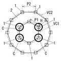
ところで、上記特許文献1には、例えば、図14に示すように、複数個(図示例では、12個)のLEDチップ1の群を実装基板2上で2つの同心状の仮想円VC1,VC2上に分けて配置してある発光装置が記載されている。ここで、図14では、各仮想円VC1,VC2上それぞれにおいて同じ個数(図示例では、6個)のLEDチップ1を等間隔で配置してあり、隣接する2つの仮想円VC1,VC2のうち外側の仮想円VC2上の任意のLEDチップ1と、そのLEDチップ1に最も近い内側の仮想円VC1の2個のLEDチップ1との間隔が等しくなっている。
しかしながら、上述の発光装置は、同一の仮想円VC1,VC2上で隣接するLEDチップ1間の間隔が小さくなると、同一の仮想円VC1,VC2上の隣接する2個のLEDチップ1からの熱負荷の影響を受けて、それら2個のLEDチップ1の間のLEDチップ1の温度が高くなってしまう。 However, when the interval between the
また、隣接する2つの仮想円VC1,VC2のうち外側の仮想円VC2上のLEDチップ1と、そのLEDチップ1に最も近い内側の仮想円VC1の2個のLEDチップ1との間隔が等しくなるには、これら3個のLEDチップ1が仮想二等辺三角形の各頂点に位置する必要があり、外側の仮想円VC2上のLEDチップ1の個数と内側の仮想円VC1上のLEDチップ1の個数とが等しくなる必要がある。このため、外側の仮想円VC2上のLEDチップ1間の間隔が大きくなり、外側の仮想円VC2上のLEDチップ1と内側の仮想円VC1上のLEDチップ1との間隔も大きくなるので、外側の仮想円VC2のLEDチップ1の方が内側の仮想円VC1のLEDチップ1に比べて、他のLEDチップ1からの熱負荷の影響が少なくなり、LEDチップ1の温度が低くなる。 In order to make the distance between the
したがって、上述のLEDチップ1の群の温度分布は内側のLEDチップ1ほど高くなる不均一な温度分布となり、当該内側のLEDチップ1のジャンクション温度が製造ばらつきを考慮して最大ジャンクション温度(例えば、130℃)よりも小さな温度に設定する許容ジャンクション温度(例えば、120℃)を超えないようにLEDチップ1への入力電力を制限する必要があり、光出力の高出力化が制限される。また、LEDチップで発生した熱を効率良く放熱させるために、上述のように、実装基板を筐体(外郭)に対して電気絶縁性および熱伝導性を有する絶縁層を介して設置することが考えられるが、例えば、JIS C 8105−1では、照明器具において人の手が触れる恐れの有る外郭の最高温度は85℃と記載されているので、製造ばらつきなどを考慮して、筐体の許容温度は80℃程度に設定するのが望ましく、LEDチップのジャンクション温度と筐体との間の熱抵抗を小さくすることが重要である。 Therefore, the temperature distribution of the group of the
ところで、複数個のLEDチップ1を用いた発光装置の信頼性は複数個のLEDチップ1の群の中で最も温度の高くなるLEDチップ1のジャンクション温度で決まるが、図14に示した構成の発光装置では、内側の仮想円VC1上に配置されたLEDチップ1のジャンクション温度で決まるので、外側の仮想円VC2上で隣接するLEDチップ1の間隔が必要以上に大きい配置となっており、発光装置におけるLEDチップの実装領域の平面サイズが大きくなってしまう。ここで、小型化および高効率化が望まれる照明器具に用いる配光制御部材には、コンパクト且つ高い光入射効率が要求され、発光装置においては、LEDチップ1の群を実装する実装領域を小さくすることが望まれる。 By the way, the reliability of the light emitting device using the plurality of
本発明は上記事由に鑑みて為されたものであり、その目的は、LEDチップの群を実装する実装領域のコンパクト化を図りながらも所望の放熱性を確保することが可能な発光装置を提供することにある。 The present invention has been made in view of the above reasons, and an object thereof is to provide a light-emitting device capable of ensuring desired heat dissipation while reducing the mounting area for mounting a group of LED chips. There is to do.
複数個のLEDチップの群と、当該複数個のLEDチップの群が一表面側に実装された実装基板とを備え、実装基板が当該実装基板の他表面側に設けられ電気絶縁性および熱伝導性を有する絶縁層を介して金属部材に熱結合された発光装置であって、複数個のLEDチップの群のうち任意の1個のLEDチップと他のn個のLEDチップそれぞれとの中心間距離をR1〜Rn、全てのLEDチップそれぞれを規定の入力電力で点灯させたときの当該他のn個のLEDチップそれぞれの発熱量をQ1〜Qnとするとき、A plurality of LED chip groups, and a mounting substrate on which the plurality of LED chip groups are mounted on one surface side, and the mounting substrate is provided on the other surface side of the mounting substrate and has electrical insulation and heat conduction A light emitting device thermally coupled to a metal member through an insulating layer having a property, between a center of any one LED chip and each of the other n LED chips among a group of a plurality of LED chips When the distance is R1 to Rn and the calorific value of each of the other n LED chips when all the LED chips are lit with the specified input power is Q1 to Qn ,

で規定した熱負荷指数Dの最大値が当該最大値とLEDチップの許容ジャンクション温度と金属部材の許容温度との関係に基づいて規定した規定値以下となるように複数個のLEDチップの群を配置してあることを特徴とする。A group of a plurality of LED chips is set such that the maximum value of the thermal load index D specified in step S is equal to or less than a specified value defined based on the relationship between the maximum value, the allowable junction temperature of the LED chip, and the allowable temperature of the metal member. It is arranged.
この発明によれば、熱負荷指数Dの最大値が当該最大値とLEDチップの許容ジャンクション温度と金属部材の許容温度との関係に基づいて規定した規定値以下となるように複数個のLEDチップの群を配置してあるので、LEDチップの群を実装する実装領域のコンパクト化を図りながらも所望の放熱性を確保することが可能となる。 According to the present invention, the plurality of LED chips are set such that the maximum value of the thermal load index D is not more than a specified value defined based on the relationship between the maximum value, the allowable junction temperature of the LED chip, and the allowable temperature of the metal member. Therefore, it is possible to secure desired heat dissipation while reducing the mounting area for mounting the LED chip group.
請求項2の発明は、請求項1の発明において、熱負荷指数Dが全てのLEDチップで同じになるように複数個のLEDチップの群を配置してあることを特徴とする。 The invention of
この発明によれば、全てのLEDチップの熱負荷が同等となり、全てのLEDチップの温度を均一化することができるから、各LEDチップの光取り出し量を一様にすることができ、各LEDチップの発光強度のばらつきを軽減することができる。 According to the present invention, the heat loads of all the LED chips are equal, and the temperatures of all the LED chips can be made uniform, so that the light extraction amount of each LED chip can be made uniform, Variations in the light emission intensity of the chip can be reduced.
請求項3の発明は、請求項1または請求項2の発明において、複数個のLEDチップの群を複数の同心状の仮想円上に分けて配置してあることを特徴とする。 The invention of
この発明によれば、LEDチップの群全体としての発光分布の均一化を図れる。 According to the present invention, the light emission distribution of the entire group of LED chips can be made uniform.
請求項4の発明は、請求項3の発明において、同一の仮想円上のLEDチップは等間隔で配置されてなることを特徴とする。 The invention of
この発明によれば、同一の仮想円上のLEDチップの間隔が等間隔でない場合に比べて、実装領域のコンパクト化を図れる。 According to the present invention, the mounting area can be made more compact than when the intervals between the LED chips on the same virtual circle are not equal.
請求項5の発明は、請求項3または請求項4の発明において、相対的に内側に位置する仮想円上のLEDチップの数に比べて相対的に外側に位置する仮想円上のLEDチップの数が多いことを特徴とする。 According to a fifth aspect of the present invention, in the third or fourth aspect of the present invention, the number of LED chips on the virtual circle relatively outside as compared with the number of LED chips on the virtual circle relatively located on the inner side. It is characterized by a large number.
この発明によれば、実装領域のコンパクト化を図れる。 According to the present invention, the mounting area can be made compact.
請求項1の発明では、LEDチップの群を実装する実装領域のコンパクト化を図りながらも所望の放熱性を確保することが可能となるという効果がある。 According to the first aspect of the present invention, there is an effect that it is possible to ensure a desired heat dissipation while reducing the mounting area for mounting the LED chip group.
(実施形態1)
本実施形態の発光装置Aは、図1に示すように、複数個(図示例では、16個)のLEDチップ1と、熱伝導性材料により形成され当該複数個のLEDチップ1の群が一表面側に実装された実装基板2と、LEDチップ1から放射された光によって励起されてLEDチップ1の発光色とは異なる色の光を放射する蛍光体を含有した透光性材料により形成されLEDチップ1を実装基板2との間に囲む形で実装基板2の上記一表面側に配設されたドーム状の色変換部材4と、LEDチップ1と色変換部材4との間に設けられLEDチップ1を封止した透光性材料からなる凸レンズ状の封止部3とを備え、実装基板2が当該実装基板2の他表面側に設けられ電気絶縁性および熱伝導性を有する絶縁層7を介して照明器具の金属部材である筐体6に熱結合されている。ここで、本実施形態の発光装置Aは、実装基板2が絶縁層7を介して筐体6に接合され、実装基板2と筐体6とが絶縁層7により電気的に絶縁され且つ熱結合されている。また、本実施形態の発光装置Aは、色変換部材4が、封止部3の光出射面との間に空気層5が形成される形で実装基板2に接合されている。(Embodiment 1)
As shown in FIG. 1, the light emitting device A of the present embodiment includes a plurality of (16 in the illustrated example)
ここで、本実施形態の発光装置Aを備えた照明器具は、図2に示すように、上述の筐体6が有底円筒状に形成されており、発光装置Aから放射される光の配光を制御する反射鏡8が筐体6内に収納されている。ここにおいて、反射鏡8は、椀状に形成され、底部に、発光装置Aが挿入される開口部8aを有している。なお、筐体6は、金属材料(例えば、Alなど)により形成されている。 Here, in the lighting fixture provided with the light emitting device A of the present embodiment, as shown in FIG. 2, the
また、本実施形態の照明器具は、筐体9の開口縁との間に反射鏡8の開口縁から外方へ延設された外鍔部8cを挟持する形で保持する円環状の保持枠10を備えている。ここで、保持枠10は、筐体9に対して複数本の取付ねじ91により固定されている。 In addition, the lighting fixture of the present embodiment has an annular holding frame that holds the
また、上述の照明器具は、発光装置Aの実装基板2が筐体6の底壁6aに対して、シリカやアルミナなどのフィラーからなる充填材を含有し且つ加熱時に低粘度化する樹脂シート(例えば、溶融シリカを高充填したエポキシ樹脂シートのような有機グリーンシート)を熱硬化させた上記絶縁層7により接合され、更に複数本の固定ねじ61により固定されている。また、上記樹脂シートは電気絶縁性を有するとともに熱伝導率が高く、しかも、加熱時の流動性が高く凹凸面への密着性が高いので、絶縁層7と実装基板2および筐体6の底壁6aとの間に空隙が発生するのを防止することができて、密着不足による熱抵抗の増大やばらつきの発生を防止することができ、ゴムシート状の放熱シートを用いる場合に比べて、LEDチップ1から筐体6までの熱抵抗を小さくすることができて放熱性が向上するとともに熱抵抗のばらつきが小さくなり、LEDチップ1のジャンクション温度の温度上昇を抑制できるから、入力電力を大きくでき、光出力の高出力化を図れる。 In addition, the above-described lighting fixture includes a resin sheet in which the
反射鏡8は、色変換部材4の光出射面から放射されて入射した光を透光性カバー8側へ反射させ狭角配光が得られるように内側面の形状が設計されており、当該内側面がドーム状の色変換部材4の頂点を焦点とする放物面状に形成されている。なお、反射鏡8の内周面の形状は特に限定するものではなく、反射鏡8は、所望の配光特性に応じて、LEDチップ1の光軸方向においてLEDチップ1から離れるにつれて開口面積が徐々に大きくなる椀状の形状に形成されていればよい。 The reflecting
反射鏡8の材料としては、例えば、LEDチップ1や蛍光体から放射される光の反射率が高い金属(例えば、Alなど)などを採用すればよく、本実施形態では、Alを採用している。また、反射鏡8の内側面は、AlやAgなどを蒸着したり、白色塗装したり、拡散反射面としたりすることで所望の反射率を確保している。なお、反射鏡8の材料は金属に限らず、高耐熱の樹脂(例えば、PBTなど)などを採用してもよい。 As a material of the reflecting
また、本実施形態の発光装置Aでは、LEDチップ1として、青色光を放射するGaN系青色LEDチップを用い、色変換部材4の蛍光体として、LEDチップ1から放射された青色光によって励起されてブロードな黄色系の光を放射する粒子状の黄色蛍光体を用いており、LEDチップ1から放射され封止部3および色変換部材4を透過した青色光と、色変換部材4の黄色蛍光体から放射された黄色光とが色変換部材4の光出射面から拡散した配光となって出射されることとなり、白色光を得ることができる。 In the light emitting device A of the present embodiment, a GaN-based blue LED chip that emits blue light is used as the
実装基板2は、セラミック基板(例えば、アルミナセラミック基板、窒化アルミニウム基板など)からなる絶縁性基板の一表面側に金属材料(例えば、Cu)からなる配線パターンが形成されている。なお、実装基板2の絶縁性基板は、セラミック基板に限らず、ガラスエポキシ樹脂基板やホーロー基板などを用いてもよいが、セラミック基板のような熱伝導性材料により形成されたものが好ましい。なお、本実施形態では、実装基板2の外周形状が円形状となっているが、円形状に限らず、多角形状でもよい。また、本実施形態では、LEDチップ1は、実装基板2の配線パターンの一部からなるダイパッド部に半田や銀ペーストなどの熱伝導性を有する接合材料を用いて接合されている。 The mounting
また、封止部3は、透光性材料としてシリコーン樹脂を採用しているが、シリコーン樹脂に限らず、エポキシ樹脂、ガラスなどを採用してもよい。 Moreover, although the sealing
また、色変換部材4は、シリコーン樹脂からなる透光性材料にLEDチップ1から放射された青色光によって励起されて黄色光を放射する粒子状の黄色蛍光体を分散させた混合材料を用いてドーム状に形成されている。なお、色変換部材4の材料として用いる透光性材料は、シリコーン樹脂に限らず、例えば、アクリル樹脂、ガラス、有機成分と無機成分とがnmレベルもしくは分子レベルで混合、結合した有機・無機ハイブリッド材料などを採用してもよい。また、色変換部材4の材料として用いる透光性材料に含有させる蛍光体も黄色蛍光体に限らず、色調整や演色性を高めるなどの目的で複数種類の蛍光体を用いてもよく、例えば、赤色蛍光体と緑色蛍光体とを用いることで演色性の高い白色光を得ることができる。ここで、複数種類の蛍光体を用いる場合には必ずしも発光色の異なる蛍光体の組み合わせに限らず、例えば、発光色はいずれも黄色で発光スペクトルの異なる複数種類の蛍光体を組み合わせてもよい。 Moreover, the
ところで、本実施形態では、複数個のLEDチップ1を同一の実装基板2に実装した構造において任意のLEDチップ1が他の全てのLEDチップ1から受ける熱負荷の影響を示す指数として熱負荷指数Dを規定し、熱負荷指数Dが規定値以下となるように複数個のLEDチップ1の群を配置した点に特徴がある。以下、説明を簡単にするために図3に示すように1個の実装基板2に同一構成の3個のLEDチップ1が実装された例で熱負荷指数Dを説明する。 By the way, in this embodiment, in a structure in which a plurality of
図3において、任意の1個のLEDチップ1に対する他のLEDチップ1からの熱は、その大部分がLEDチップ1直下の実装基板2に伝わる。ここで、実装基板の熱伝導率は一様であるから、実装基板2に伝わった熱は実装基板2におけるLEDチップ1直下の表面を基点として実装基板2内の全方向に一様に伝わる。したがって、上記基点から同一距離の球面上の任意点を通過する熱量は等しい値となるから、同一球面上の単位面積当たりの熱量は等しい値となる。しかして、LEDチップ1で発生した熱量をQ、球面の面積をS、球面上の単位面積当たりの熱量をqとすれば、Q=S・qとなる。ここにおいて、球面の面積Sは、上記基点からの距離の2乗に比例するから、他のLEDチップ1から任意のLEDチップ1に寄与する伝熱量はLEDチップ1間の距離の2乗に反比例する。 In FIG. 3, most of the heat from another
そこで、図3における3個のLEDチップ1を同一の規定の入力電力で点灯させる場合、同図における中央のLEDチップ1を任意のLEDチップ1とし、同図における右上のLEDチップ1の発熱量をQ1、任意のLEDチップ1との中心間距離をR1、同図における左上のLEDチップ1の発熱量をQ2、任意のLEDチップ1との中心間距離をR2とするとき、熱負荷指数Dを、D=Q1/R12+Q2/R22と規定する。Therefore, when the three
上述の例はLEDチップ1の群が3個のLEDチップ1で構成される例であるが、LEDチップ1の個数は複数個であれば何個でもよいから、複数個のLEDチップ1の群のうち任意の1個のLEDチップ1と他のn個のLEDチップ1それぞれとの中心間距離をR1〜Rn、全てのLEDチップ1それぞれを規定の入力電力で点灯させたときの当該他のn個のLEDチップそれぞれの発熱量をQ1〜Qnとして、熱負荷指数Dを一般化すると、下記式(1)で表される。The above-described example is an example in which the group of
また、本実施形態の発光装置Aでは、上記式(1)で規定した熱負荷指数Dの最大値が当該最大値とLEDチップ1の許容ジャンクション温度と金属部材である筐体6の許容温度との関係に基づいて規定した規定値以下となるように複数個のLEDチップ1の群を配置してある。ここにおいて、本願発明者らは、この規定値を規定するにあたって、まず、図4に示すようなLEDチップ1の群の多数(図示例では、10)の配置例それぞれについて熱負荷指数Dの最大値(熱負荷指数max値)、および、LEDチップ1のジャンクションと筐体6との間の熱抵抗Rjbを求めたところ、図5に示すように熱負荷指数max値と熱抵抗Rjbとが線形関係を有するという知見を得た。なお、熱負荷指数Dを求めるにあたっては、LEDチップ1を照明器具用に用いられる高輝度の青色LEDチップとし、規定の入力電力を1.3W(電流350mA)とした。 Further, in the light emitting device A of the present embodiment, the maximum value of the thermal load index D defined by the above formula (1) is the maximum value, the allowable junction temperature of the
ここにおいて、LEDチップ1および封止部3の信頼性を確保するための目安としてLEDチップ1の許容ジャンクションを120℃、筐体6の許容温度を80℃とすると、許容される熱抵抗Rjbは、Rjb=(120−80)/1.3≒30℃/Wとなる。これに対して、図5から、熱抵抗Rjbが30℃/Wとなるときの熱負荷指数max値は、0.69であり、熱負荷指数max値が0.69以下であれば、熱抵抗Rjbが30℃/W以下となり、コンパクト化を図りながらも所望の信頼性および放熱性を確保できるので、本実施形態では、上記規定値を0.69としてある。 Here, if the allowable junction of the
なお、本実施形態では、16個のLEDチップ1が実装基板2の上記一表面側において図1(b)に示すように1つの仮想円VC上(仮想円VCの円周上)に等間隔で配置されているが、仮想円VCの直径φを13.94mm、仮想円VC上で隣り合うLEDチップ1の中心間距離Pを2.72mmとしてあり、各LEDチップ1の熱負荷指数Dが全て0.58となり、熱負荷指数max値が0.58、熱抵抗Rjbの最大値が29℃/Wとなり、全てのLEDチップ1の温度が略等しくなっている。したがって、筐体6の温度が80℃であるとすれば、LEDチップ1のジャンクション温度は118℃となり、高い信頼性を確保することができる。 In the present embodiment, 16
以上説明した本実施形態の発光装置Aでは、上記式(1)で規定した熱負荷指数Dの最大値が当該最大値とLEDチップ1の許容ジャンクション温度と金属部材である筐体6の許容温度との関係に基づいて規定した規定値以下となるように複数個のLEDチップ1の群を配置してあるので、LEDチップ1の群を実装する実装領域のコンパクト化を図りながらも所望の放熱性を確保することが可能となる。しかして、本実施形態の発光装置Aを適用した照明器具では、配光制御部材である反射鏡8の小型化による照明器具の小型化を図りつつ照明器具全体としての外部への光取り出し効率を向上させることができる。 In the light emitting device A of the present embodiment described above, the maximum value of the thermal load index D defined by the above formula (1) is the maximum value, the allowable junction temperature of the
また、本実施形態の発光装置Aは、熱負荷指数Dが全てのLEDチップ1で同じになるように複数個のLEDチップ1の群を配置してあるので、全てのLEDチップ1の熱負荷が同等となり、全てのLEDチップ1の温度を均一化することができるから、各LEDチップ1の光取り出し量を一様にすることができ、各LEDチップ1の発光強度のばらつきを軽減することができ、輝度むらを軽減することができる。 Further, in the light emitting device A of the present embodiment, the group of the plurality of
(実施形態2)
本実施形態の発光装置Aの基本構成は実施形態1と略同じであり、図6に示すように、複数個(図示例では、16個)のLEDチップ1の群を複数(図示例では2つ)の同心状の仮想円VC1,VC2上に分けて配置してある点などが相違する。なお、実施形態1と同様の構成要素には同一の符号を付して説明を適宜省略する。(Embodiment 2)
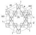
The basic configuration of the light emitting device A of the present embodiment is substantially the same as that of the first embodiment. As shown in FIG. 6, a plurality (16 in the illustrated example) of groups of
本実施形態では、内側の仮想円VC1上(仮想円VC1の円周上)に6個のLEDチップ1を等間隔で配置し、外側の仮想円VC2上(仮想円VC2の円周上)に10個のLEDチップ1を等間隔で配置してあるが、内側の仮想円VC1の直径を7mm、外側の仮想円VC2の直径を13.4mm、内側の仮想円VC1上で隣り合うLEDチップ1の中心間距離P1を3.5mm、外側の仮想円VC2上で隣り合うLEDチップ1の中心間距離P2を4.3mmとしてあるので、内側の仮想円VC1上の6個のLEDチップ1と外側の仮想円VC2上の10個のLEDチップ1との組み合わせにおいて最近接するLEDチップ1の中心間距離Hが3.5mmとなっており、熱負荷指数max値が図6において太線の丸で囲んだ4個のLEDチップ1の0.683となっており、これら4個のLEDチップ1に関する熱抵抗Rjbが29.7℃/Wとなり、他のLEDチップ1では熱抵抗Rjbが29.7℃/Wよりも小さな値となっている(つまり、熱抵抗Rjbの最大値が30℃/Wよりも小さな29.7℃/Wとなっている)。 In the present embodiment, six
しかして、本実施形態の発光装置Aにおいても、実施形態1と同様、上記式(1)で規定した熱負荷指数Dの最大値が当該最大値とLEDチップ1の許容ジャンクション温度と金属部材である筐体6の許容温度との関係に基づいて規定した規定値以下となるように複数個のLEDチップ1の群を配置してあるので、LEDチップ1の群を実装する実装領域のコンパクト化を図りながらも所望の放熱性を確保することが可能となる。 Thus, also in the light emitting device A of the present embodiment, as in the first embodiment, the maximum value of the thermal load index D defined by the above formula (1) is the maximum value, the allowable junction temperature of the
また、本実施形態の発光装置Aでは、複数個のLEDチップ1の群を2つの同心状の仮想円VC1,VC2上に分けて配置してあるので、LEDチップ1の群全体としての発光分布の均一化を図れる。なお、同心状の仮想円の数は特に限定するものではない。 Further, in the light emitting device A of the present embodiment, the group of the plurality of
ここで、図7に示すように、色変換部材4(蛍光体キャップ)の光軸M1と実装基板2の上記一表面との交点をO2とし、本実施形態の発光装置Aにおいて、上記交点O2を仮想円VC1,VC2の中心と一致させ(要するに、上記実装領域の中心と一致させ)、交点O2から色変換部材4に向かう直線と光軸M1とのなす角度をθ(℃)とした場合の角度θと色変換部材4表面の輝度との関係を図8(a)に示し、実施形態1の発光装置Aにおいて、上記交点O2を仮想円VCの中心と一致させ(要するに、上記実装領域の中心と一致させ)、交点O2から色変換部材4に向かう直線と光軸M1とのなす角度をθ(℃)とした場合の角度θと色変換部材4表面の輝度との関係を図8(b)に示す。 Here, as shown in FIG. 7, the intersection point between the optical axis M1 of the color conversion member 4 (phosphor cap) and the one surface of the mounting
図8(a),(b)から、本実施形態の発光装置Aのように、複数個のLEDチップ1の群を2つの同心状の仮想円VC1,VC2上に分けて配置することにより、実施形態1のように複数個のLEDチップ1を1つの仮想円VC上にのみに配置する場合に比べて、色変換部材4表面の輝度むらを軽減できるので、照明器具による照射面の照度むらを低減することができる。 8A and 8B, by arranging a group of a plurality of
また、本実施形態の発光装置では、同一の仮想円VC1上のLEDチップ1、仮想円VC2上のLEDチップそれぞれが等間隔で配置されているので、同一の仮想円VC,VC2上のLEDチップ1の間隔が等間隔でない場合に比べて、実装領域のコンパクト化を図れる。また、本実施形態の発光装置では、相対的に内側に位置する仮想円VC1上のLEDチップ1の数に比べて相対的に外側に位置する仮想円VC2上のLEDチップ1の数が多いので、実装領域のコンパクト化を図れる。 Further, in the light emitting device of the present embodiment, the
(実施形態3)
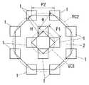
本実施形態の発光装置Aの基本構成は実施形態2と略同じであり、図9に示すように、LEDチップ1の個数が12個であり、内側の仮想円VC1上に6個のLEDチップ1を等間隔で配置し(要するに、正6角形の各頂点にLEDチップ1の中心が位置している)、外側の仮想円VC2上に6個のLEDチップ1を等間隔で配置してある(要するに、正6角形の各頂点にLEDチップ1の中心が位置している)点などが相違する。なお、実施形態2と同様の構成要素には同一の符号を付して説明を適宜省略する。(Embodiment 3)
The basic configuration of the light-emitting device A of the present embodiment is substantially the same as that of the second embodiment. As shown in FIG. 9, the number of
本実施形態では、内側の仮想円VC1の直径を7mm、外側の仮想円VC2の直径を12.1mm、内側の仮想円VC1上で隣り合うLEDチップ1の中心間距離P1を3.5mm、外側の仮想円VC2上で隣り合うLEDチップ1の中心間距離P2を6.05mmとしてあるので、内側の仮想円VC1上の6個のLEDチップ1と外側の仮想円VC2上の6個のLEDチップ1との組み合わせにおいて最近接するLEDチップ1の中心間距離Hが3.5mmとなっており、熱負荷指数max値が内側の仮想円VC1上の6個のLEDチップ1の0.62となっており、これら6個のLEDチップ1に関する熱抵抗Rjbが29.6℃/Wとなり、外側の仮想円VC2上の6個のLEDチップ1に関する熱抵抗Rjbが27℃/Wとなっている(つまり、熱抵抗Rjbの最大値が30℃/Wよりも小さな29.6℃/Wとなっている)。 In the present embodiment, the inner virtual circle VC1 has a diameter of 7 mm, the outer virtual circle VC2 has a diameter of 12.1 mm, and the center-to-center distance P1 between the
しかして、本実施形態の発光装置Aにおいても、実施形態2と同様、上記式(1)で規定した熱負荷指数Dの最大値が当該最大値とLEDチップ1の許容ジャンクション温度と金属部材である筐体6の許容温度との関係に基づいて規定した規定値以下となるように複数個のLEDチップ1の群を配置してあるので、LEDチップ1の群を実装する実装領域のコンパクト化を図りながらも所望の放熱性を確保することが可能となる。 Thus, also in the light emitting device A of the present embodiment, as in the second embodiment, the maximum value of the thermal load index D defined by the above formula (1) is the maximum value, the allowable junction temperature of the
(実施形態4)
本実施形態の発光装置Aの基本構成は実施形態2と略同じであり、図10に示すように、LEDチップ1の個数が12個であり、内側の仮想円VC1上に4個のLEDチップ1を等間隔で配置し(要するに、正方形の各頂点にLEDチップ1の中心が位置している)、外側の仮想円VC2上に8個のLEDチップ1を等間隔で配置してある(要するに、正8角形の各頂点にLEDチップ1の中心が位置している)点などが相違する。なお、実施形態2と同様の構成要素には同一の符号を付して説明を適宜省略する。(Embodiment 4)
The basic configuration of the light emitting device A of the present embodiment is substantially the same as that of the second embodiment. As shown in FIG. 10, the number of
本実施形態では、内側の仮想円VC1の直径を5.3mm、外側の仮想円VC2の直径を12.1mm、内側の仮想円VC1上で隣り合うLEDチップ1の中心間距離P1を3.75mm、外側の仮想円VC2上で隣り合うLEDチップ1の中心間距離P2を4.64mmとしてあるので、内側の仮想円VC1上の4個のLEDチップ1と外側の仮想円VC2上の8個のLEDチップ1との組み合わせにおいて最近接するLEDチップ1の中心間距離Hが3.75mmとなっており、熱負荷指数max値が内側の仮想円VC1上の4個のLEDチップ1の0.59となっており、これら4個のLEDチップ1に関する熱抵抗Rjbが29.4℃/Wとなり、外側の仮想円VC2上の8個のLEDチップ1に関する熱抵抗Rjbが26.6℃/Wとなっている(つまり、熱抵抗Rjbの最大値が30℃/Wよりも小さな29.4℃/Wとなっている)。 In this embodiment, the inner virtual circle VC1 has a diameter of 5.3 mm, the outer virtual circle VC2 has a diameter of 12.1 mm, and the center-to-center distance P1 of the
しかして、本実施形態の発光装置Aにおいても、実施形態2と同様、上記式(1)で規定した熱負荷指数Dの最大値が当該最大値とLEDチップ1の許容ジャンクション温度と金属部材である筐体6の許容温度との関係に基づいて規定した規定値以下となるように複数個のLEDチップ1の群を配置してあるので、LEDチップ1の群を実装する実装領域のコンパクト化を図りながらも所望の放熱性を確保することが可能となる。 Thus, also in the light emitting device A of the present embodiment, as in the second embodiment, the maximum value of the thermal load index D defined by the above formula (1) is the maximum value, the allowable junction temperature of the
(実施形態5)
本実施形態の発光装置Aの基本構成は実施形態2と略同じであり、図11に示すように、LEDチップ1の個数が15個であり、内側の仮想円VC1上に5個のLEDチップ1を等間隔で配置し(要するに、正5角形の各頂点にLEDチップ1の中心が位置している)、外側の仮想円VC2上に10個のLEDチップ1を等間隔で配置してある(要するに、正10角形の各頂点にLEDチップ1の中心が位置している)点などが相違する。なお、実施形態2と同様の構成要素には同一の符号を付して説明を適宜省略する。(Embodiment 5)
The basic configuration of the light emitting device A of the present embodiment is substantially the same as that of the second embodiment. As shown in FIG. 11, the number of
本実施形態では、内側の仮想円VC1の直径を5.95mm、外側の仮想円VC2の直径を13.45mm、内側の仮想円VC1上で隣り合うLEDチップ1の中心間距離P1を3.5mm、外側の仮想円VC2上で隣り合うLEDチップ1の中心間距離P2を4.16mmとしてあるので、内側の仮想円VC1上の5個のLEDチップ1と外側の仮想円VC2上の10個のLEDチップ1との組み合わせにおいて最近接するLEDチップ1の中心間距離Hが4.0mmとなっており、熱負荷指数max値が内側の仮想円VC1上の5個のLEDチップ1の0.67となっており、これら5個のLEDチップ1に関する熱抵抗Rjbが29.5℃/Wとなり、外側の仮想円VC2上の10個のLEDチップ1に関する熱抵抗Rjbが26.6℃/Wとなっている(つまり、熱抵抗Rjbの最大値が30℃/Wよりも小さな29.5℃/Wとなっている)。 In the present embodiment, the inner virtual circle VC1 has a diameter of 5.95 mm, the outer virtual circle VC2 has a diameter of 13.45 mm, and the center-to-center distance P1 between
しかして、本実施形態の発光装置Aにおいても、実施形態2と同様、上記式(1)で規定した熱負荷指数Dの最大値が当該最大値とLEDチップ1の許容ジャンクション温度と金属部材である筐体6の許容温度との関係に基づいて規定した規定値以下となるように複数個のLEDチップ1の群を配置してあるので、LEDチップ1の群を実装する実装領域のコンパクト化を図りながらも所望の放熱性を確保することが可能となる。 Thus, also in the light emitting device A of the present embodiment, as in the second embodiment, the maximum value of the thermal load index D defined by the above formula (1) is the maximum value, the allowable junction temperature of the
(実施形態6)
本実施形態の発光装置Aの基本構成は実施形態2と略同じであり、図12に示すように、LEDチップ1の個数が24個であり、内側の仮想円VC1上に8個のLEDチップ1を等間隔で配置し(要するに、正8角形の各頂点にLEDチップ1の中心が位置している)、外側の仮想円VC2上に16個のLEDチップ1を等間隔で配置してある(要するに、正16角形の各頂点にLEDチップ1の中心が位置している)点などが相違する。なお、実施形態2と同様の構成要素には同一の符号を付して説明を適宜省略する。(Embodiment 6)
The basic configuration of the light emitting device A of the present embodiment is substantially the same as that of the second embodiment. As shown in FIG. 12, the number of
本実施形態では、内側の仮想円VC1の直径を10.45mm、外側の仮想円VC2の直径を20.5mm、内側の仮想円VC1上で隣り合うLEDチップ1の中心間距離P1を4.0mm、外側の仮想円VC2上で隣り合うLEDチップ1の中心間距離P2を4.0mmとしてあるので、内側の仮想円VC1上の8個のLEDチップ1と外側の仮想円VC2上の16個のLEDチップ1との組み合わせにおいて最近接するLEDチップ1の中心間距離Hが5.03mmとなっており、熱負荷指数max値が内側の仮想円VC1上の8個のLEDチップ1の0.53となっており、これら8個のLEDチップ1に関する熱抵抗Rjbが26.7℃/Wとなり、外側の仮想円VC2上の16個のLEDチップ1に関する熱抵抗Rjbが25.7℃/Wとなっている(つまり、熱抵抗Rjbの最大値が30℃/Wよりも小さな26.7℃/Wとなっている)。 In this embodiment, the inner virtual circle VC1 has a diameter of 10.45 mm, the outer virtual circle VC2 has a diameter of 20.5 mm, and the center-to-center distance P1 of the
しかして、本実施形態の発光装置Aにおいても、実施形態2と同様、上記式(1)で規定した熱負荷指数Dの最大値が当該最大値とLEDチップ1の許容ジャンクション温度と金属部材である筐体6の許容温度との関係に基づいて規定した規定値以下となるように複数個のLEDチップ1の群を配置してあるので、LEDチップ1の群を実装する実装領域のコンパクト化を図りながらも所望の放熱性を確保することが可能となる。 Thus, also in the light emitting device A of the present embodiment, as in the second embodiment, the maximum value of the thermal load index D defined by the above formula (1) is the maximum value, the allowable junction temperature of the
(実施形態7)
本実施形態の発光装置Aの基本構成は実施形態1と略同じであり、図13に示すように、12個のLEDチップ1が3行×4列の2次元アレイ状に配置してある(3行×4列の仮想正方格子の各格子点にLEDチップ1の中心が位置している)点などが相違する。なお、実施形態1と同様の構成要素には同一の符号を付して説明を適宜省略する。(Embodiment 7)
The basic configuration of the light emitting device A of the present embodiment is substantially the same as that of the first embodiment, and as shown in FIG. 13, 12
本実施形態では、LEDチップ1の中心間距離Pを4.0mmとしてあり、熱負荷指数max値が0.55となっており、熱負荷指数Dが0.55のLEDチップ1に関する熱抵抗Rjbが28.9℃/Wとなっている(つまり、熱抵抗Rjbの最大値が30℃/Wよりも小さな28.9℃/Wとなっている)。 In this embodiment, the center-to-center distance P of the
しかして、本実施形態の発光装置Aにおいても、実施形態1と同様、上記式(1)で規定した熱負荷指数Dの最大値が当該最大値とLEDチップ1の許容ジャンクション温度と金属部材である筐体6の許容温度との関係に基づいて規定した規定値以下となるように複数個のLEDチップ1の群を配置してあるので、LEDチップ1の群を実装する実装領域のコンパクト化を図りながらも所望の放熱性を確保することが可能となる。 Thus, also in the light emitting device A of the present embodiment, as in the first embodiment, the maximum value of the thermal load index D defined by the above formula (1) is the maximum value, the allowable junction temperature of the
ところで、上述の各実施形態では、LEDチップ1として、青色光を放射する青色LEDチップを採用しているが、LEDチップ1は青色光を放射するものに限らず、例えば、紫外光を放射するものでもよく、色変換部材4における蛍光体の発光色も特に限定するものではない。 By the way, in each above-mentioned embodiment, although the blue LED chip which radiates | emits blue light is employ | adopted as
A 発光装置
1 LEDチップ
2 実装基板
6 筐体(金属部材)
7 絶縁層
VC,VC1,VC2 仮想円A
7 Insulation layer VC, VC1, VC2 Virtual circle
Claims (5)
Translated fromJapanesePriority Applications (1)
| Application Number | Priority Date | Filing Date | Title |
|---|---|---|---|
| JP2008190083AJP5270991B2 (en) | 2008-07-23 | 2008-07-23 | Light emitting device and lighting apparatus |
Applications Claiming Priority (1)
| Application Number | Priority Date | Filing Date | Title |
|---|---|---|---|
| JP2008190083AJP5270991B2 (en) | 2008-07-23 | 2008-07-23 | Light emitting device and lighting apparatus |
Publications (2)
| Publication Number | Publication Date |
|---|---|
| JP2010027514Atrue JP2010027514A (en) | 2010-02-04 |
| JP5270991B2 JP5270991B2 (en) | 2013-08-21 |
Family
ID=41733136
Family Applications (1)
| Application Number | Title | Priority Date | Filing Date |
|---|---|---|---|
| JP2008190083AActiveJP5270991B2 (en) | 2008-07-23 | 2008-07-23 | Light emitting device and lighting apparatus |
Country Status (1)
| Country | Link |
|---|---|
| JP (1) | JP5270991B2 (en) |
Cited By (7)
| Publication number | Priority date | Publication date | Assignee | Title |
|---|---|---|---|---|
| EP2372764A2 (en)* | 2010-04-01 | 2011-10-05 | LG Innotek Co., Ltd | Inter-chip distance in a multi-chip LED package |
| JP2012109405A (en)* | 2010-11-17 | 2012-06-07 | Panasonic Corp | Structure and lighting device including the structure |
| JP2013004814A (en)* | 2011-06-17 | 2013-01-07 | Panasonic Corp | Led unit |
| JP2013098416A (en)* | 2011-11-02 | 2013-05-20 | Toshiba Lighting & Technology Corp | Light emitting module and lighting device |
| JP2013157615A (en)* | 2013-03-07 | 2013-08-15 | Toshiba Corp | Light emitting device module |
| JP2013172147A (en)* | 2012-02-17 | 2013-09-02 | Shogen Koden Kofun Yugenkoshi | Light-emitting diode element |
| WO2014118835A1 (en)* | 2013-01-29 | 2014-08-07 | パナソニック株式会社 | Ultraviolet light emitting device |
Citations (3)
| Publication number | Priority date | Publication date | Assignee | Title |
|---|---|---|---|---|
| JP2004265664A (en)* | 2003-02-28 | 2004-09-24 | Toshiba Lighting & Technology Corp | Lighting equipment and lighting equipment |
| JP2005216495A (en)* | 2004-01-27 | 2005-08-11 | Matsushita Electric Works Ltd | Led unit with base |
| JP2007059260A (en)* | 2005-08-25 | 2007-03-08 | Toshiba Lighting & Technology Corp | Illumination device and illumination fixture |
- 2008
- 2008-07-23JPJP2008190083Apatent/JP5270991B2/enactiveActive
Patent Citations (3)
| Publication number | Priority date | Publication date | Assignee | Title |
|---|---|---|---|---|
| JP2004265664A (en)* | 2003-02-28 | 2004-09-24 | Toshiba Lighting & Technology Corp | Lighting equipment and lighting equipment |
| JP2005216495A (en)* | 2004-01-27 | 2005-08-11 | Matsushita Electric Works Ltd | Led unit with base |
| JP2007059260A (en)* | 2005-08-25 | 2007-03-08 | Toshiba Lighting & Technology Corp | Illumination device and illumination fixture |
Cited By (11)
| Publication number | Priority date | Publication date | Assignee | Title |
|---|---|---|---|---|
| EP2372764A2 (en)* | 2010-04-01 | 2011-10-05 | LG Innotek Co., Ltd | Inter-chip distance in a multi-chip LED package |
| JP2011216891A (en)* | 2010-04-01 | 2011-10-27 | Lg Innotek Co Ltd | Light-emitting device package and lighting system |
| US9520383B2 (en) | 2010-04-01 | 2016-12-13 | Lg Innotek Co., Ltd. | Light emitting device package and lighting system |
| JP2012109405A (en)* | 2010-11-17 | 2012-06-07 | Panasonic Corp | Structure and lighting device including the structure |
| JP2013004814A (en)* | 2011-06-17 | 2013-01-07 | Panasonic Corp | Led unit |
| JP2013098416A (en)* | 2011-11-02 | 2013-05-20 | Toshiba Lighting & Technology Corp | Light emitting module and lighting device |
| JP2013172147A (en)* | 2012-02-17 | 2013-09-02 | Shogen Koden Kofun Yugenkoshi | Light-emitting diode element |
| KR101874001B1 (en)* | 2012-02-17 | 2018-07-05 | 에피스타 코포레이션 | Light-emitting diode device |
| WO2014118835A1 (en)* | 2013-01-29 | 2014-08-07 | パナソニック株式会社 | Ultraviolet light emitting device |
| JP2014146689A (en)* | 2013-01-29 | 2014-08-14 | Panasonic Corp | Ultraviolet ray generator |
| JP2013157615A (en)* | 2013-03-07 | 2013-08-15 | Toshiba Corp | Light emitting device module |
Also Published As
| Publication number | Publication date |
|---|---|
| JP5270991B2 (en) | 2013-08-21 |
Similar Documents
| Publication | Publication Date | Title |
|---|---|---|
| JP5327601B2 (en) | Light emitting module and lighting device | |
| JP5459623B2 (en) | Lighting device | |
| US8672512B2 (en) | Omni reflective optics for wide angle emission LED light bulb | |
| JP5414859B2 (en) | Light bulb shaped lamp and lighting device | |
| JP5999391B2 (en) | Light emitting device, illumination light source, and illumination device | |
| US20120300430A1 (en) | Light-emitting module and lighting apparatus | |
| JP2012195404A (en) | Light-emitting device and luminaire | |
| JP5270991B2 (en) | Light emitting device and lighting apparatus | |
| JP2006156187A (en) | LED light source device and LED bulb | |
| EP2672513B1 (en) | Multichip package structure for generating a symmetrical and uniform light-blending source | |
| JP6277510B2 (en) | Light emitting module, lighting device and lighting fixture | |
| JP2009032466A (en) | Lighting device | |
| JP5815859B2 (en) | Light source device and lighting device | |
| JP2017045951A (en) | LED module and lighting fixture including the same | |
| JP6508556B2 (en) | lighting equipment | |
| JP2010251213A (en) | Light emitting module and lighting device | |
| CN110291632B (en) | LED unit | |
| JP5330944B2 (en) | Light emitting device | |
| JP5320627B2 (en) | Lamp with lamp and lighting equipment | |
| JP5243883B2 (en) | Light emitting device and lighting apparatus | |
| JP2010272687A (en) | Lighting device and lighting fixture | |
| US20110121340A1 (en) | Light emitting device package | |
| KR101082924B1 (en) | Traffic light using led lighting source | |
| CN204284979U (en) | Lighting device | |
| KR101315703B1 (en) | Lighting device |
Legal Events
| Date | Code | Title | Description |
|---|---|---|---|
| RD04 | Notification of resignation of power of attorney | Free format text:JAPANESE INTERMEDIATE CODE: A7424 Effective date:20100806 | |
| A621 | Written request for application examination | Free format text:JAPANESE INTERMEDIATE CODE: A621 Effective date:20110323 | |
| A711 | Notification of change in applicant | Free format text:JAPANESE INTERMEDIATE CODE: A712 Effective date:20120112 | |
| A977 | Report on retrieval | Free format text:JAPANESE INTERMEDIATE CODE: A971007 Effective date:20120831 | |
| A131 | Notification of reasons for refusal | Free format text:JAPANESE INTERMEDIATE CODE: A131 Effective date:20120925 | |
| A521 | Written amendment | Free format text:JAPANESE INTERMEDIATE CODE: A523 Effective date:20121126 | |
| TRDD | Decision of grant or rejection written | ||
| A01 | Written decision to grant a patent or to grant a registration (utility model) | Free format text:JAPANESE INTERMEDIATE CODE: A01 Effective date:20130416 | |
| A61 | First payment of annual fees (during grant procedure) | Free format text:JAPANESE INTERMEDIATE CODE: A61 Effective date:20130510 | |
| R150 | Certificate of patent or registration of utility model | Free format text:JAPANESE INTERMEDIATE CODE: R150 Ref document number:5270991 Country of ref document:JP Free format text:JAPANESE INTERMEDIATE CODE: R150 |