JP2010021204A - Semiconductor device and manufacturing method thereof - Google Patents
Semiconductor device and manufacturing method thereofDownload PDFInfo
- Publication number
- JP2010021204A JP2010021204AJP2008178168AJP2008178168AJP2010021204AJP 2010021204 AJP2010021204 AJP 2010021204AJP 2008178168 AJP2008178168 AJP 2008178168AJP 2008178168 AJP2008178168 AJP 2008178168AJP 2010021204 AJP2010021204 AJP 2010021204A
- Authority
- JP
- Japan
- Prior art keywords
- insulating film
- film
- block
- oxygen
- main components
- Prior art date
- Legal status (The legal status is an assumption and is not a legal conclusion. Google has not performed a legal analysis and makes no representation as to the accuracy of the status listed.)
- Pending
Links
Images


Classifications
- H—ELECTRICITY
- H10—SEMICONDUCTOR DEVICES; ELECTRIC SOLID-STATE DEVICES NOT OTHERWISE PROVIDED FOR
- H10D—INORGANIC ELECTRIC SEMICONDUCTOR DEVICES
- H10D30/00—Field-effect transistors [FET]
- H10D30/60—Insulated-gate field-effect transistors [IGFET]
- H10D30/69—IGFETs having charge trapping gate insulators, e.g. MNOS transistors
- H—ELECTRICITY
- H10—SEMICONDUCTOR DEVICES; ELECTRIC SOLID-STATE DEVICES NOT OTHERWISE PROVIDED FOR
- H10D—INORGANIC ELECTRIC SEMICONDUCTOR DEVICES
- H10D30/00—Field-effect transistors [FET]
- H10D30/01—Manufacture or treatment
- H10D30/021—Manufacture or treatment of FETs having insulated gates [IGFET]
- H10D30/0413—Manufacture or treatment of FETs having insulated gates [IGFET] of FETs having charge-trapping gate insulators, e.g. MNOS transistors
- H—ELECTRICITY
- H10—SEMICONDUCTOR DEVICES; ELECTRIC SOLID-STATE DEVICES NOT OTHERWISE PROVIDED FOR
- H10D—INORGANIC ELECTRIC SEMICONDUCTOR DEVICES
- H10D30/00—Field-effect transistors [FET]
- H10D30/60—Insulated-gate field-effect transistors [IGFET]
- H10D30/69—IGFETs having charge trapping gate insulators, e.g. MNOS transistors
- H10D30/694—IGFETs having charge trapping gate insulators, e.g. MNOS transistors characterised by the shapes, relative sizes or dispositions of the gate electrodes
- H—ELECTRICITY
- H10—SEMICONDUCTOR DEVICES; ELECTRIC SOLID-STATE DEVICES NOT OTHERWISE PROVIDED FOR
- H10D—INORGANIC ELECTRIC SEMICONDUCTOR DEVICES
- H10D64/00—Electrodes of devices having potential barriers
- H10D64/01—Manufacture or treatment
- H10D64/031—Manufacture or treatment of data-storage electrodes
- H10D64/037—Manufacture or treatment of data-storage electrodes comprising charge-trapping insulators
- H—ELECTRICITY
- H10—SEMICONDUCTOR DEVICES; ELECTRIC SOLID-STATE DEVICES NOT OTHERWISE PROVIDED FOR
- H10D—INORGANIC ELECTRIC SEMICONDUCTOR DEVICES
- H10D64/00—Electrodes of devices having potential barriers
- H10D64/60—Electrodes characterised by their materials
- H10D64/66—Electrodes having a conductor capacitively coupled to a semiconductor by an insulator, e.g. MIS electrodes
- H10D64/68—Electrodes having a conductor capacitively coupled to a semiconductor by an insulator, e.g. MIS electrodes characterised by the insulator, e.g. by the gate insulator
- H10D64/681—Electrodes having a conductor capacitively coupled to a semiconductor by an insulator, e.g. MIS electrodes characterised by the insulator, e.g. by the gate insulator having a compositional variation, e.g. multilayered
- H10D64/685—Electrodes having a conductor capacitively coupled to a semiconductor by an insulator, e.g. MIS electrodes characterised by the insulator, e.g. by the gate insulator having a compositional variation, e.g. multilayered being perpendicular to the channel plane
Landscapes
- Semiconductor Memories (AREA)
- Non-Volatile Memory (AREA)
Abstract
Description
Translated fromJapanese本発明は、半導体装置及びその製造方法に関する。 The present invention relates to a semiconductor device and a manufacturing method thereof.
電荷蓄積層に電荷トラップ用の電荷蓄積絶縁膜を用いた電荷トラップ型の不揮発性半導体メモリが提案されている(特許文献1参照)。この電荷トラップ型の不揮発性半導体メモリでは、トンネル絶縁膜を通して電荷蓄積絶縁膜に注入された電荷を、電荷蓄積絶縁膜中のトラップ準位にトラップさせることで、電荷蓄積絶縁膜に電荷が蓄積される。代表的な電荷トラップ型の不揮発性半導体メモリとしては、MONOS型或いはSONOS型の不揮発性半導体メモリが知られている。 A charge trap type nonvolatile semiconductor memory using a charge storage insulating film for charge trapping as a charge storage layer has been proposed (see Patent Document 1). In this charge trap type nonvolatile semiconductor memory, charges injected into the charge storage insulating film through the tunnel insulating film are trapped in the trap level in the charge storage insulating film, so that the charge is stored in the charge storage insulating film. The As a typical charge trapping type nonvolatile semiconductor memory, a MONOS type or SONOS type nonvolatile semiconductor memory is known.
しかしながら、電荷トラップ型の不揮発性半導体メモリでは、電荷蓄積絶縁膜と制御ゲート電極との間に設けられたブロック絶縁膜の構成や形成方法について、必ずしも最適化がはかられているとは言えない。
本発明は、ブロック絶縁膜の最適化をはかることが可能な半導体装置及びその製造方法を提供することを目的としている。 An object of the present invention is to provide a semiconductor device capable of optimizing a block insulating film and a manufacturing method thereof.
本発明の第1の視点に係る半導体装置は、半導体基板上に形成されたトンネル絶縁膜と、前記トンネル絶縁膜上に形成された電荷蓄積絶縁膜と、前記電荷蓄積絶縁膜上に形成されたブロック絶縁膜と、前記ブロック絶縁膜上に形成された制御ゲート電極と、を備えた半導体装置であって、前記ブロック絶縁膜は、金属元素及び酸素を主成分として含有する第1の絶縁膜と、シリコン及び酸素を主成分として含有する第2の絶縁膜と、前記第1の絶縁膜と前記第2の絶縁膜との間に形成され且つ前記金属元素、シリコン及び酸素を主成分として含有する界面層と、を含む。 A semiconductor device according to a first aspect of the present invention is formed on a tunnel insulating film formed on a semiconductor substrate, a charge storage insulating film formed on the tunnel insulating film, and the charge storage insulating film. A semiconductor device comprising a block insulating film and a control gate electrode formed on the block insulating film, wherein the block insulating film includes a first insulating film containing a metal element and oxygen as main components; A second insulating film containing silicon and oxygen as main components; and formed between the first insulating film and the second insulating film and containing the metal elements, silicon and oxygen as main components. An interface layer.
本発明の第2の視点に係る半導体装置は、半導体基板上に形成されたトンネル絶縁膜と、前記トンネル絶縁膜上に形成された電荷蓄積絶縁膜と、前記電荷蓄積絶縁膜上に形成されたブロック絶縁膜と、前記ブロック絶縁膜上に形成された制御ゲート電極と、を備えた半導体装置であって、前記ブロック絶縁膜は、金属元素及び酸素を主成分として含有する第1の絶縁膜と、シリコン及び酸素を主成分として含有する第2の絶縁膜と、前記第1の絶縁膜と前記第2の絶縁膜との間に形成され且つ窒素を含有する界面層と、を含み、前記界面層は、前記第1の絶縁膜及び前記第2の絶縁膜よりも高い窒素濃度を有する。 A semiconductor device according to a second aspect of the present invention is formed on a tunnel insulating film formed on a semiconductor substrate, a charge storage insulating film formed on the tunnel insulating film, and the charge storage insulating film. A semiconductor device comprising a block insulating film and a control gate electrode formed on the block insulating film, wherein the block insulating film includes a first insulating film containing a metal element and oxygen as main components; A second insulating film containing silicon and oxygen as main components, and an interface layer formed between the first insulating film and the second insulating film and containing nitrogen. The layer has a higher nitrogen concentration than the first insulating film and the second insulating film.
本発明の第3の視点に係る半導体装置は、半導体基板上に形成されたトンネル絶縁膜と、前記トンネル絶縁膜上に形成された電荷蓄積絶縁膜と、前記電荷蓄積絶縁膜上に形成されたブロック絶縁膜と、前記ブロック絶縁膜上に形成された制御ゲート電極と、を備えた半導体装置であって、前記ブロック絶縁膜は、金属元素及び酸素を主成分として含有する第1の絶縁膜と、シリコン及び酸素を主成分として含有する第2の絶縁膜と、前記第1の絶縁膜と前記第2の絶縁膜との間に形成され且つ希ガス元素及びハロゲン元素から選択された所定元素を含有する界面層と、を含み、前記界面層は、前記第1の絶縁膜及び前記第2の絶縁膜よりも高い前記所定元素の濃度を有する。 A semiconductor device according to a third aspect of the present invention includes a tunnel insulating film formed on a semiconductor substrate, a charge storage insulating film formed on the tunnel insulating film, and the charge storage insulating film. A semiconductor device comprising a block insulating film and a control gate electrode formed on the block insulating film, wherein the block insulating film includes a first insulating film containing a metal element and oxygen as main components; A second insulating film containing silicon and oxygen as main components, and a predetermined element formed between the first insulating film and the second insulating film and selected from a rare gas element and a halogen element. And the interface layer has a higher concentration of the predetermined element than the first insulating film and the second insulating film.
本発明の第4の視点に係る半導体装置の製造方法は、半導体基板上に形成されたトンネル絶縁膜と、前記トンネル絶縁膜上に形成された電荷蓄積絶縁膜と、前記電荷蓄積絶縁膜上に形成されたブロック絶縁膜と、前記ブロック絶縁膜上に形成された制御ゲート電極と、を備えた半導体装置の製造方法であって、前記ブロック絶縁膜を形成する工程は、金属元素及び酸素を主成分として含有する第1の絶縁膜を形成する工程と、前記第1の絶縁膜上にシリコン及び酸素を主成分として含有する第2の絶縁膜を形成する工程と、前記第1の絶縁膜及び前記第2の絶縁膜に対して酸化性雰囲気で熱処理を施す工程と、を備える。 A method of manufacturing a semiconductor device according to a fourth aspect of the present invention includes a tunnel insulating film formed on a semiconductor substrate, a charge storage insulating film formed on the tunnel insulating film, and the charge storage insulating film. A method of manufacturing a semiconductor device comprising a formed block insulating film and a control gate electrode formed on the block insulating film, wherein the step of forming the block insulating film mainly comprises a metal element and oxygen. A step of forming a first insulating film containing as a component, a step of forming a second insulating film containing silicon and oxygen as main components on the first insulating film, the first insulating film and And heat-treating the second insulating film in an oxidizing atmosphere.
本発明の第5の視点に係る半導体装置の製造方法は、半導体基板上に形成されたトンネル絶縁膜と、前記トンネル絶縁膜上に形成された電荷蓄積絶縁膜と、前記電荷蓄積絶縁膜上に形成されたブロック絶縁膜と、前記ブロック絶縁膜上に形成された制御ゲート電極と、を備えた半導体装置の製造方法であって、前記ブロック絶縁膜を形成する工程は、第1の成膜雰囲気で、金属元素及び酸素を主成分として含有する第1の絶縁膜を形成する工程と、前記第1の絶縁膜上にシリコン及び酸素を主成分として含有する第2の絶縁膜を形成する工程と、前記第1の成膜雰囲気よりも酸化力の強い第2の成膜雰囲気で、前記第2の絶縁膜上に金属元素及び酸素を主成分として含有する第3の絶縁膜を形成する工程と、を備える。 A method of manufacturing a semiconductor device according to a fifth aspect of the present invention includes a tunnel insulating film formed on a semiconductor substrate, a charge storage insulating film formed on the tunnel insulating film, and the charge storage insulating film. A method for manufacturing a semiconductor device comprising a formed block insulating film and a control gate electrode formed on the block insulating film, wherein the step of forming the block insulating film includes a first film formation atmosphere. A step of forming a first insulating film containing a metal element and oxygen as main components, and a step of forming a second insulating film containing silicon and oxygen as main components on the first insulating film; Forming a third insulating film containing a metal element and oxygen as main components on the second insulating film in a second film forming atmosphere having a stronger oxidizing power than the first film forming atmosphere; .
本発明によれば、ブロック絶縁膜の最適化をはかることが可能となる。 According to the present invention, it is possible to optimize the block insulating film.
以下、本発明の実施形態を図面を参照して説明する。なお、以下の各実施形態では、電荷蓄積層に電荷トラップ用の電荷蓄積絶縁膜を用いた電荷トラップ型の不揮発性半導体メモリについて説明する。 Hereinafter, embodiments of the present invention will be described with reference to the drawings. In each of the following embodiments, a charge trap type nonvolatile semiconductor memory using a charge storage insulating film for charge trapping as a charge storage layer will be described.
(実施形態1)
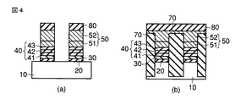
図1〜図5は、本実施形態に係る半導体装置(不揮発性半導体メモリ)の基本的な製造方法を模式的に示した断面図である。図1(a)〜図5(a)はチャネル長方向(ビット線方向)に沿った断面図であり、図1(b)〜図5(b)はチャネル幅方向(ワード線方向)に沿った断面図である。(Embodiment 1)
1 to 5 are cross-sectional views schematically showing a basic manufacturing method of a semiconductor device (nonvolatile semiconductor memory) according to this embodiment. 1A to 5A are cross-sectional views along the channel length direction (bit line direction), and FIGS. 1B to 5B are along the channel width direction (word line direction). FIG.
まず、図1に示すように、所望の不純物元素がされたドーピングされた半導体基板(シリコン基板)10上に、トンネル絶縁膜20として、厚さ5nm程度のシリコン酸化膜を熱酸化法によって形成する。続いて、トンネル絶縁膜20上に、電荷蓄積絶縁膜30として、厚さ5nm程度のシリコン窒化膜をCVD(chemical vapor deposition)法で形成する。 First, as shown in FIG. 1, a silicon oxide film having a thickness of about 5 nm is formed as a
次に、電荷蓄積絶縁膜30上に、下層絶縁膜41、中間絶縁膜42及び上層絶縁膜43が積層されたブロック絶縁膜40を形成する。ブロック絶縁膜40には、下層絶縁膜41と中間絶縁膜42との間に形成された界面層(図示せず)、及び上層絶縁膜43と中間絶縁膜42との間に形成された界面層(図示せず)が含まれている。なお、ブロック絶縁膜40の構成及び形成方法の詳細については後述する。 Next, the
次に、図2に示すように、ブロック絶縁膜40上に、下層制御ゲート電極膜51として、厚さ30nm程度のポリシリコン膜をCVD法で形成する。続いて、下層制御ゲート電極膜51上に、マスク膜60をCVD法で形成する。さらに、マスク膜60上に、ビット線方向に延伸したフォトレジストパターン(図示せず)を形成する。このフォトレジストパターンをマスクとして用いて、マスク膜60、下層制御ゲート電極膜51、ブロック絶縁膜40、電荷蓄積絶縁膜30、トンネル絶縁膜20及び半導体基板10をRIE(reactive ion etching)法によってエッチングする。その結果、ビット線方向に延伸した深さ100nm程度の素子分離溝が形成され、隣接する素子分離溝の間に素子領域が形成される。素子分離溝の幅及び素子領域の幅はいずれも、50nm程度である。その後、全面に素子分離絶縁膜としてシリコン酸化膜を堆積し、素子分離溝を素子分離絶縁膜で埋める。さらに、CMP(chemical mechanical polishing)法によって素子分離絶縁膜を平坦化し、マスク膜60を露出させる。これにより、素子分離溝が素子分離絶縁膜で埋められた素子分離領域70が得られる。 Next, as shown in FIG. 2, a polysilicon film having a thickness of about 30 nm is formed as a lower control
次に、図3に示すように、マスク膜60をウェットエッチングによって選択的に除去し、下層制御ゲート電極膜51を露出させる。続いて、全面に上層制御ゲート電極膜52として、多結晶シリコン及びタングステンシリサイドの積層膜(厚さ100nm程度)をCVD法で形成する。 Next, as shown in FIG. 3, the
次に、図4に示すように、マスク膜80としてシリコン窒化膜をCVD法で形成する。さらに、マスク膜80上に、ワード線方向に延伸したフォトレジストパターン(図示せず)を形成する。このフォトレジストパターンをマスクとして用いて、マスク膜80、上層制御ゲート電極膜52、下層制御ゲート電極膜51、ブロック絶縁膜40、電荷蓄積絶縁膜30及びトンネル絶縁膜20をRIE法によってエッチングする。これにより、下層制御ゲート電極膜51及び上層制御ゲート電極膜52で形成された制御ゲート電極50のパターンが得られる。制御ゲート電極50のパターン幅及び制御ゲート電極50間のスペース幅は、いずれも50nm程度である。 Next, as shown in FIG. 4, a silicon nitride film is formed as a
次に、図5に示すように、上記のようにして得られたゲート構造をマスクとして用いて、半導体基板10の表面領域に不純物元素をイオン注入する。さらに、熱処理を行って、ソース/ドレイン領域(不純物拡散層)90を形成する。このようにして、半導体基板10上に形成されたトンネル絶縁膜20と、トンネル絶縁膜20上に形成された電荷蓄積絶縁膜30と、電荷蓄積絶縁膜30上に形成されたブロック絶縁膜40と、ブロック絶縁膜40上に形成された制御ゲート電極50と、ソース/ドレイン領域(不純物拡散層)90とを備えた電荷トラップ型のメモリセルトランジスタが得られる。その後、CVD法によって層間絶縁膜100を形成する。さらに、公知の技術を用いて配線等を形成して、半導体装置(不揮発性半導体メモリ)が得られる。 Next, as shown in FIG. 5, an impurity element is ion-implanted into the surface region of the
上述した電荷トラップ型の不揮発性半導体メモリセル(メモリセルトランジスタ)では、制御ゲート電極50と半導体基板10との間に適当な電圧を印加することで、トンネル絶縁膜20を介して半導体基板10と電荷蓄積絶縁膜30との間で電荷の充放電が行われる。具体的には、トンネル絶縁膜20を通して電荷蓄積絶縁膜30に注入された電荷を、電荷蓄積絶縁膜30中のトラップ準位にトラップさせることで、電荷蓄積絶縁膜30に電荷が蓄積される。 In the above-described charge trap type nonvolatile semiconductor memory cell (memory cell transistor), an appropriate voltage is applied between the
なお、上述した半導体装置では、図5(b)に示すように、電荷蓄積絶縁膜30及びブロック絶縁膜40が素子分離領域70によって分断されているが、これらが素子分離領域70によって分断されていない構成を採用することも可能である。 In the semiconductor device described above, as shown in FIG. 5B, the charge
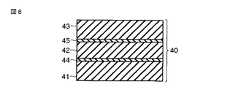
図6は、ブロック絶縁膜40の詳細な構成を模式的に示した断面図である。 FIG. 6 is a cross-sectional view schematically showing a detailed configuration of the
ブロック絶縁膜40は、下層絶縁膜41、中間絶縁膜42及び上層絶縁膜43の積層構造を有している。下層絶縁膜41及び上層絶縁膜43は、少なくとも金属元素及び酸素を主成分として含有する。一般的には、下層絶縁膜41及び上層絶縁膜43として金属酸化物膜が用いられる。中間絶縁膜42は、少なくともシリコン及び酸素を主成分として含有する。一般的には、中間絶縁膜42としてシリコン酸化膜が用いられる。中間絶縁膜42には、窒素等の元素が含有されていてもよい。下層絶縁膜41の誘電率及び上層絶縁膜43の誘電率は、中間絶縁膜42の誘電率よりも高い。また、ブロック絶縁膜40には、下層絶縁膜41と中間絶縁膜42との間に形成された界面層44と、上層絶縁膜43と中間絶縁膜42との間に形成された界面層45が含まれている。 The
上述したように、ブロック絶縁膜40は、下層絶縁膜41、中間絶縁膜42及び上層絶縁膜43の積層構造を有している。下層絶縁膜41及び上層絶縁膜43として用いられる金属酸化物膜は、誘電率が高く、高電界(高電圧)印加時におけるリーク耐性(高電界リーク耐性)に優れている。しかしながら、金属酸化物膜は、シリコン酸化膜に比べてトラップ準位密度が高いため、低電界(低電圧)印加時におけるリーク耐性(低電界リーク耐性)はシリコン酸化膜よりも劣る。本実施形態のブロック絶縁膜40は、金属酸化物を主成分とする下層絶縁膜41と、シリコン酸化物を主成分とする中間絶縁膜42と、金属酸化物を主成分とする上層絶縁膜43との積層構造を有している。そのため、下層絶縁膜41及び上層絶縁膜43によって高電界リーク耐性を確保し、中間絶縁膜42によって低電界リーク耐性を確保することができる。したがって、ブロック絶縁膜40のリーク電流を抑制することが可能である。また、以下に述べるように、界面層44及び45を設けることにより、より一層、リーク電流を抑制することが可能である。 As described above, the
図7は、図6に示したブロック絶縁膜40の電荷トラップ準位密度の分布を模式的に示した図である。図7に示すように、中間絶縁膜42は、下層絶縁膜41及び上層絶縁膜43に比べてトラップ準位密度が非常に低い。また、界面層44及び界面層45では、中間絶縁膜42、下層絶縁膜41及び上層絶縁膜43に比べてトラップ準位密度が非常に高くなっている。例えば、界面層44及び45のトラップ準位密度は、1×10¹¹〜1×10¹⁵/cm2程度である。FIG. 7 is a diagram schematically showing the distribution of the charge trap level density of the
図8は、本実施形態のメモリセルトランジスタの書き込み動作時におけるエネルギーバンド構造を示した図である。図9は、本実施形態の比較例に係るメモリセルトランジスタの書き込み動作時におけるエネルギーバンド構造を示した図である。 FIG. 8 is a diagram showing an energy band structure during the write operation of the memory cell transistor of this embodiment. FIG. 9 is a diagram showing an energy band structure during the write operation of the memory cell transistor according to the comparative example of the present embodiment.
上述したように、本実施形態のメモリセルトランジスタでは、図6に示すように、下層絶縁膜41と中間絶縁膜42との間に界面層44が形成され、上層絶縁膜43と中間絶縁膜42との間に界面層45が形成されている。そのため、図8に示すように、書き込み動作に伴い、界面層44及び45のトラップ準位に電荷(図の例では電子)がトラップされる。その結果、トラップされた電荷(特に、界面層44にトラップされた電荷)によって、下層絶縁膜41に印加される電界が弱められる。したがって、トンネル電流に対する実効的なバリア性が向上し、ブロック絶縁膜のリーク電流を抑制することができる。 As described above, in the memory cell transistor of this embodiment, as shown in FIG. 6, the
なお、メモリセルトランジスタの消去動作時にも、上述した原理と同様の原理により、ブロック絶縁膜のリーク電流が抑制される。すなわち、消去動作に伴い、界面層44及び45のトラップ準位に電荷がトラップされ、トラップされた電荷(特に、界面層45にトラップされた電荷)によって、上層絶縁膜43に印加される電界が弱められる。その結果、トンネル電流に対する実効的なバリア性が向上し、ブロック絶縁膜のリーク電流を抑制することができる。 Note that also during the erase operation of the memory cell transistor, the leakage current of the block insulating film is suppressed by the same principle as described above. That is, with the erasing operation, charges are trapped in the trap levels of the interface layers 44 and 45, and the electric field applied to the upper insulating
また、界面層44は下層絶縁膜41と中間絶縁膜42との界面に形成され、界面層45は上層絶縁膜43と中間絶縁膜42との界面に形成される。そのため、界面層44及び45は電荷蓄積絶縁膜30及び制御ゲート電極50対して一定の距離があり、電荷のデトラップによる電荷保持特性の劣化を抑制することも可能である。 The
以上のように、本実施形態のブロック絶縁膜40は、下層絶縁膜41、中間絶縁膜42及び上層絶縁膜43の積層構造を有し、且つ、トラップ準位密度の高い界面層44及び45を有している。したがって、ブロック絶縁膜40のリーク電流を大幅に抑制することができ、特性や信頼性に優れた不揮発性半導体メモリを得ることができる。 As described above, the
以下、本実施形態におけるメモリセルトランジスタの具体的な構成及び製造方法について説明する。 Hereinafter, a specific configuration and manufacturing method of the memory cell transistor in the present embodiment will be described.
(具体例1)
図10は、本実施形態の第1の具体例の製造方法の一部を模式的に示した断面図である。なお、基本的な製造方法は、図1〜図5に示した方法と同様であり、主としてブロック絶縁膜の製造方法について説明する。(Specific example 1)
FIG. 10 is a cross-sectional view schematically showing a part of the manufacturing method of the first specific example of the present embodiment. The basic manufacturing method is the same as the method shown in FIGS. 1 to 5, and the manufacturing method of the block insulating film will be mainly described.
図1の工程で電荷蓄積絶縁膜30を形成した後、図10(a)に示すように、電荷蓄積絶縁膜30上に、ブロック絶縁膜の下層絶縁膜41となる金属酸化物膜を形成する。金属酸化物膜としてはアルミニウム酸化物膜(アルミナ膜)を用いる。具体的には、トリメチルアルミニウム及び水蒸気を原料ガスとして用いたALD(atomic layer deposition)法により、成膜温度300℃で、厚さ4nm程度のアルミナ膜41を形成する。窒素雰囲気中にて、1000℃で1分間の熱処理を行った後、アルミナ膜41上に、ブロック絶縁膜の中間絶縁膜42となるシリコン酸化膜を形成する。具体的には、亜酸化窒素及びジクロルシランを原料ガスとして用いたCVD(chemical vapor deposition)法により、成膜温度800℃で、厚さ3nm程度のシリコン酸化膜42を形成する。続いて、シリコン酸化膜42上に、ブロック絶縁膜の上層絶縁膜43となる金属酸化物膜を形成する。金属酸化物膜としてはアルミナ膜を用い、ALD法により厚さ4nm程度のアルミナ膜43を形成する。アルミナ膜43の具体的な成膜条件は、上述したアルミナ膜41の成膜条件と同じである。 After the charge
次に、図10(b)に示すように、窒素雰囲気中にて、1000℃で1分間の熱処理を行う。この熱処理により、アルミナ膜(下層絶縁膜)41とシリコン酸化膜(中間絶縁膜)42との界面に界面層44aが形成され、アルミナ膜(上層絶縁膜)43とシリコン酸化膜(中間絶縁膜)42との界面に界面層45aが形成される。界面層44a及び45aはいずれも、アルミニウム、シリコン及び酸素を主成分として含有する。すなわち、熱処理によるアルミナ膜とシリコン酸化膜との界面反応によりアルミニウムシリケイトが形成され、界面層44a及び45aが形成される。なお、一般的に言えば、界面層44aは、シリコン、酸素及び下層絶縁膜41に含有される金属元素を主成分として含有する。界面層45aは、シリコン、酸素及び上層絶縁膜43に含有される金属元素を主成分として含有する。 Next, as shown in FIG. 10B, heat treatment is performed at 1000 ° C. for 1 minute in a nitrogen atmosphere. By this heat treatment, an
以後の工程は、図2〜図5に示した工程と同様であり、図5に示すようなメモリセルトランジスタが形成される。 The subsequent steps are the same as those shown in FIGS. 2 to 5, and a memory cell transistor as shown in FIG. 5 is formed.
図11は、図10(b)の工程の熱処理温度と、ブロック絶縁膜40のリーク電流密度との関係を示した図である。ブロック絶縁膜40には、書き込み動作時の電界と同等の電界が印加されている。図11に示すように、熱処理温度が増加すると、リーク電流は減少する。これは、電荷トラップの起源となるアルミニウムシリケイトが、熱処理温度が高いほど形成されやすいためである。ただし、熱処理温度が1100℃以上になると、熱劣化によってメモリセルトランジスタの信頼性低下が起こる。したがって、熱処理温度は900℃から1100℃の範囲であることが好ましい。 FIG. 11 is a diagram showing the relationship between the heat treatment temperature in the step of FIG. 10B and the leakage current density of the
このように、本具体例では、アルミナ膜(下層絶縁膜)41、シリコン酸化膜(中間絶縁膜)42及びアルミナ膜(上層絶縁膜)43を形成した後に熱処理を行うことで、界面反応が生じる。この界面反応によって形成された金属シリケイトが、トラップ準位密度の高い界面層44a及び45aとなる。したがって、すでに述べたように、ブロック絶縁膜40のリーク電流を大幅に抑制することができ、特性や信頼性に優れた不揮発性半導体メモリを得ることが可能となる。 Thus, in this specific example, an interface reaction occurs by performing heat treatment after forming the alumina film (lower insulating film) 41, the silicon oxide film (intermediate insulating film) 42, and the alumina film (upper insulating film) 43. . The metal silicate formed by this interface reaction becomes the interface layers 44a and 45a having a high trap state density. Therefore, as already described, the leakage current of the
(具体例2)
図12は、本実施形態の第2の具体例の製造方法の一部を模式的に示した断面図である。なお、基本的な製造方法は、図1〜図5に示した方法と同様であり、主としてブロック絶縁膜の製造方法について説明する。(Specific example 2)
FIG. 12 is a cross-sectional view schematically showing a part of the manufacturing method of the second specific example of the present embodiment. The basic manufacturing method is the same as the method shown in FIGS. 1 to 5, and the manufacturing method of the block insulating film will be mainly described.
図1の工程で電荷蓄積絶縁膜30を形成した後、図12(a)に示すように、電荷蓄積絶縁膜30上に、ブロック絶縁膜の下層絶縁膜41となる非晶質の金属酸化物膜を形成する。金属酸化物膜としてはハフニウム酸化物膜を用いる。具体的には、テトラエチルメチルアミノハフニウム及び水蒸気を原料ガスとして用いたALD法により、成膜温度200℃で、厚さ4nm程度のハフニウム酸化物膜41を形成する。続いて、ハフニウム酸化物膜41上に、ブロック絶縁膜の中間絶縁膜42となるシリコン酸化膜を形成する。具体的には、亜酸化窒素及びジクロルシランを原料ガスとして用いたCVD法により、成膜温度800℃で、厚さ3nm程度のシリコン酸化膜42を形成する。続いて、シリコン酸化膜42上に、ブロック絶縁膜の上層絶縁膜43となる非晶質の金属酸化物膜を形成する。金属酸化物膜としてはハフニウム酸化物膜を用い、ALD法により厚さ4nm程度のハフニウム酸化物膜43を形成する。ハフニウム酸化物膜43の具体的な成膜条件は、上述したハフニウム酸化物膜41の成膜条件と同じである。 After the charge
次に、図12(b)に示すように、窒素雰囲気中にて、800℃で1分間の熱処理を行う。この熱処理により、ハフニウム酸化物膜(下層絶縁膜)41とシリコン酸化膜(中間絶縁膜)42との界面に界面層44bが形成され、ハフニウム酸化物膜(上層絶縁膜)43とシリコン酸化膜(中間絶縁膜)42との界面に界面層45bが形成される。界面層44b及び45bはいずれも、ハフニウム、シリコン及び酸素を主成分として含有する。すなわち、熱処理によるハフニウム酸化物膜とシリコン酸化膜との界面反応によりハフニウムシリケイトが形成され、界面層44b及び45bが形成される。一般的に言えば、界面層44bは、シリコン、酸素及び下層絶縁膜41に含有される金属元素を主成分として含有する。界面層45bは、シリコン、酸素及び上層絶縁膜43に含有される金属元素を主成分として含有する。 Next, as shown in FIG. 12B, heat treatment is performed at 800 ° C. for 1 minute in a nitrogen atmosphere. By this heat treatment, an
以後の工程は、図2〜図5に示した工程と同様であり、図5に示すようなメモリセルトランジスタが形成される。 The subsequent steps are the same as those shown in FIGS. 2 to 5, and a memory cell transistor as shown in FIG. 5 is formed.
このように、本具体例では、ハフニウム酸化物膜(下層絶縁膜)41、シリコン酸化膜(中間絶縁膜)42及びハフニウム酸化物膜(上層絶縁膜)43を形成した後に熱処理を行うことで、界面反応が生じる。この界面反応によって形成された金属シリケイトが、トラップ準位密度の高い界面層44b及び45bとなる。したがって、すでに述べたように、ブロック絶縁膜40のリーク電流を大幅に抑制することができ、特性や信頼性に優れた不揮発性半導体メモリを得ることが可能となる。 Thus, in this specific example, the heat treatment is performed after the hafnium oxide film (lower insulating film) 41, the silicon oxide film (intermediate insulating film) 42, and the hafnium oxide film (upper insulating film) 43 are formed. Interfacial reaction occurs. The metal silicate formed by this interface reaction becomes the interface layers 44b and 45b having a high trap level density. Therefore, as already described, the leakage current of the
また、本具体例では、下層絶縁膜41及び上層絶縁膜43は、非晶質のハフニウム酸化物膜で形成されている。図12(b)の熱処理により、ハフニウム酸化物膜41及び43は結晶化するが、シリコン酸化膜(中間絶縁膜)42は非晶質状態を維持する。そのため、ハフニウム酸化物膜41とシリコン酸化膜42との界面、及びハフニウム酸化物膜43とシリコン酸化膜42との界面で、応力による歪みが発生する。その結果、トラップ準位密度をより増加させることができる。したがって、ブロック絶縁膜40のリーク電流をより確実に抑制することが可能となる。 In this specific example, the lower insulating
(具体例3)
図13は、本実施形態の第3の具体例の製造方法の一部を模式的に示した断面図である。なお、基本的な製造方法は、図1〜図5に示した方法と同様であり、主としてブロック絶縁膜の製造方法について説明する。(Specific example 3)
FIG. 13 is a cross-sectional view schematically showing a part of the manufacturing method of the third specific example of the present embodiment. The basic manufacturing method is the same as the method shown in FIGS. 1 to 5, and the manufacturing method of the block insulating film will be mainly described.
図1の工程で電荷蓄積絶縁膜30を形成した後、図13(a)に示すように、電荷蓄積絶縁膜30上に、ブロック絶縁膜の下層絶縁膜41となる金属酸化物膜を形成する。金属酸化物膜としてはハフニウム酸化物膜を用いる。具体的には、テトラエチルメチルアミノハフニウム及び水蒸気を原料ガスとして用いたALD法により、成膜温度300℃で、厚さ4nm程度のハフニウム酸化物膜41を形成する。続いて、ハフニウム酸化物膜41の表面領域を、窒素ラジカルによって窒化する。このラジカル窒化処理は、圧力10Paの窒素を含む雰囲気下で行われ、処理温度は300℃である。このラジカル窒化処理により、ハフニウム酸化物膜41の表面に、窒素を含有する界面層44cが形成される。 After the charge
次に、図13(b)に示すように、界面層44c上に、ブロック絶縁膜の中間絶縁膜42となるシリコン酸化膜を形成する。具体的には、亜酸化窒素及びジクロルシランを原料ガスとして用いたCVD法により、成膜温度800℃で、厚さ3nm程度のシリコン酸化膜42を形成する。続いて、シリコン酸化膜42の表面領域を、窒素ラジカルによって窒化する。このラジカル窒化処理の条件は、上述したハフニウム酸化物膜41のラジカル窒化処理の条件と同じである。このラジカル窒化処理により、シリコン酸化膜42の表面に、窒素を含有する界面層45cが形成される。 Next, as shown in FIG. 13B, a silicon oxide film to be the intermediate insulating
次に、図13(c)に示すように、界面層45c上に、ブロック絶縁膜の上層絶縁膜43となる金属酸化物膜を形成する。金属酸化物膜としてはハフニウム酸化物膜を用い、ALD法により厚さ4nm程度のハフニウム酸化物膜43を形成する。ハフニウム酸化物膜43の具体的な成膜条件は、上述したハフニウム酸化物膜41の成膜条件と同じである。 Next, as shown in FIG. 13C, a metal oxide film to be the upper insulating
このようにして、ハフニウム酸化物膜(下層絶縁膜)41とシリコン酸化膜(中間絶縁膜)42との界面に界面層44cが形成され、ハフニウム酸化物膜(上層絶縁膜)43とシリコン酸化膜(中間絶縁膜)42との界面に界面層45cが形成されたブロック絶縁膜40が得られる。界面層44c及び45cはいずれも、ハフニウム酸化物膜(下層絶縁膜)41、シリコン酸化膜(中間絶縁膜)42及びハフニウム酸化物膜(上層絶縁膜)43よりも高い窒素濃度を有している。 Thus, an
以後の工程は、図2〜図5に示した工程と同様であり、図5に示すようなメモリセルトランジスタが形成される。 The subsequent steps are the same as those shown in FIGS. 2 to 5, and a memory cell transistor as shown in FIG. 5 is formed.
このように、本具体例では、ハフニウム酸化物膜(下層絶縁膜)41の表面領域を窒化して界面層44cを形成し、シリコン酸化膜(中間絶縁膜)42の表面領域を窒化して界面層45cを形成する。界面層44c及び45cには、窒素に起因して多数の電荷トラップが形成される。例えば、窒素の導入によって多数のダングリングボンドが生成され、これが電荷トラップとして作用する。その結果、トラップ準位密度の高い界面層44c及び45cが得られる。したがって、すでに述べたように、ブロック絶縁膜40のリーク電流を大幅に抑制することができ、特性や信頼性に優れた不揮発性半導体メモリを得ることが可能となる。 Thus, in this specific example, the surface region of the hafnium oxide film (lower insulating film) 41 is nitrided to form the
なお、上述した例では、窒化処理としてラジカル窒化を用いたが、例えば熱窒化処理を用いてもよい。 In the above-described example, radical nitridation is used as the nitriding treatment. However, for example, thermal nitriding treatment may be used.
(具体例4)
図14は、本実施形態の第4の具体例の製造方法の一部を模式的に示した断面図である。なお、基本的な製造方法は、図1〜図5に示した方法と同様であり、主としてブロック絶縁膜の製造方法について説明する。(Specific example 4)
FIG. 14 is a cross-sectional view schematically showing a part of the manufacturing method of the fourth specific example of the present embodiment. The basic manufacturing method is the same as the method shown in FIGS. 1 to 5, and the manufacturing method of the block insulating film will be mainly described.
図1の工程で電荷蓄積絶縁膜30を形成した後、図14(a)に示すように、電荷蓄積絶縁膜30上に、ブロック絶縁膜の下層絶縁膜41となる金属酸化物膜を形成する。金属酸化物膜としてはハフニウム酸化物膜を用いる。具体的には、テトラエチルメチルアミノハフニウム及び水蒸気を原料ガスとして用いたALD法により、成膜温度300℃で、厚さ4nm程度のハフニウム酸化物膜41を形成する。続いて、アルゴンガス雰囲気下において、1000℃で1分間の熱処理を行う。この熱処理により、ハフニウム酸化物膜41の表面に、アルゴン(Ar)を含有する界面層44dが形成される。 After forming the charge
次に、図14(b)に示すように、界面層44c上に、ブロック絶縁膜の中間絶縁膜42となるシリコン酸化膜を形成する。具体的には、亜酸化窒素及びジクロルシランを原料ガスとして用いたCVD法により、成膜温度800℃で、厚さ3nm程度のシリコン酸化膜42を形成する。続いて、アルゴンガス雰囲気下において、1000℃で1分間の熱処理を行う。このラジカル窒化処理により、シリコン酸化膜42の表面に、アルゴン(Ar)を含有する界面層45dが形成される。 Next, as shown in FIG. 14B, a silicon oxide film to be the intermediate insulating
次に、図14(c)に示すように、界面層45d上に、ブロック絶縁膜の上層絶縁膜43となる金属酸化物膜を形成する。金属酸化物膜としてはハフニウム酸化物膜を用い、ALD法により厚さ4nm程度のハフニウム酸化物膜43を形成する。ハフニウム酸化物膜43の具体的な成膜条件は、上述したハフニウム酸化物膜41の成膜条件と同じである。 Next, as shown in FIG. 14C, a metal oxide film to be the upper insulating
このようにして、ハフニウム酸化物膜(下層絶縁膜)41とシリコン酸化膜(中間絶縁膜)42との界面に界面層44dが形成され、ハフニウム酸化物膜(上層絶縁膜)43とシリコン酸化膜(中間絶縁膜)42との界面に界面層45dが形成されたブロック絶縁膜40が得られる。界面層44d及び45dはいずれも、ハフニウム酸化物膜(下層絶縁膜)41、シリコン酸化膜(中間絶縁膜)42及びハフニウム酸化物膜(上層絶縁膜)43よりも高いアルゴン濃度を有している。 Thus, the
以後の工程は、図2〜図5に示した工程と同様であり、図5に示すようなメモリセルトランジスタが形成される。 The subsequent steps are the same as those shown in FIGS. 2 to 5, and a memory cell transistor as shown in FIG. 5 is formed.
このように、本具体例では、ハフニウム酸化物膜(下層絶縁膜)41の表面にアルゴンを含有する界面層44dを形成し、シリコン酸化膜(中間絶縁膜)42の表面にアルゴンを含有する界面層45dを形成する。界面層44d及び45dでは、アルゴンに起因して多数の電荷トラップが形成される。例えば、アルゴンの導入によって絶縁膜を構成する原子のネットワーク構造に歪みが生じ、これが電荷トラップとして作用する。その結果、トラップ準位密度の高い界面層44d及び45dが得られる。したがって、すでに述べたように、ブロック絶縁膜40のリーク電流を大幅に抑制することができ、特性や信頼性に優れた不揮発性半導体メモリを得ることが可能となる。 Thus, in this example, the
なお、上述した例では、アルゴン雰囲気下で熱処理を行ったが、一般的には、希ガス元素及びハロゲン元素から選択された所定元素を含んだ雰囲気下で熱処理を行うことが可能である。この場合にも、上述した構成と同様の構成が得られ、上述した効果と同様の効果が得られる。例えば、希ガス元素としてはアルゴン、クリプトン或いはキセノン等を用いることができ、ハロゲン元素としては臭素等を用いることができる。特に、イオン半径の大きな元素を用いた場合には、上述したネットワーク構造の歪みが大きくなり、界面層44d及び45dのトラップ準位密度を高めることができる。 In the above-described example, the heat treatment is performed in an argon atmosphere. However, in general, the heat treatment can be performed in an atmosphere containing a predetermined element selected from a rare gas element and a halogen element. Also in this case, the same configuration as that described above is obtained, and the same effect as that described above is obtained. For example, argon, krypton, xenon, or the like can be used as the rare gas element, and bromine or the like can be used as the halogen element. In particular, when an element having a large ion radius is used, the above-described distortion of the network structure is increased, and the trap level density of the interface layers 44d and 45d can be increased.
以上、本発明の第1の実施形態について説明したが、本実施形態は以下のような変更が可能である。 Although the first embodiment of the present invention has been described above, the present embodiment can be modified as follows.
上述した実施形態では、下層絶縁膜41と中間絶縁膜42との界面及び上層絶縁膜43と中間絶縁膜42との界面にのみ、電荷トラップ準位密度が高い層(界面層44及び45)を設けていたが、界面層44及び45に加えてさらに中間絶縁膜42中にも電荷トラップ準位密度が高い層を設けてもよい。このような構成であっても、上述した実施形態と同様の効果を得ることが可能である。 In the above-described embodiment, layers (interface layers 44 and 45) having a high charge trap level density are provided only at the interface between the lower insulating
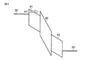
また、上述した実施形態では、ブロック絶縁膜40を下層絶縁膜41、中間絶縁膜42及び上層絶縁膜43で形成したが、ブロック絶縁膜40の構成は上述した実施形態の構成には限定されない。一般的には、ブロック絶縁膜40は、金属元素及び酸素を主成分として含有する第1の絶縁膜と、シリコン及び酸素を主成分として含有する第2の絶縁膜と、第1の絶縁膜と第2の絶縁膜との界面に形成された界面層とを含む。界面層は、第1の絶縁膜及び第2の絶縁膜よりもトラップ準位密度が高い。また、第1の絶縁膜の誘電率は、第2の絶縁膜の誘電率よりも高い。例えば、第1の絶縁膜には、上述した実施形態で述べたような金属酸化物膜を用いることができ、第2の絶縁膜には、上述した実施形態で述べたようなシリコン酸化膜を用いることができる。界面層にも、上述した実施形態で述べたような界面層を用いることができる。以下、図15を参照して具体的に説明する。 In the above-described embodiment, the
図15(a)は、ブロック絶縁膜40の第1の変更例の構成を模式的に示した断面図である。図15(a)に示すように、ブロック絶縁膜40は、金属元素及び酸素を主成分として含有する下層絶縁膜(第1の絶縁膜)411と、シリコン及び酸素を主成分として含有する上層絶縁膜(第2の絶縁膜)412と、下層絶縁膜411と上層絶縁膜412との界面に形成された界面層413とを有している。このような構成でも、上述した実施形態と同様、高いトラップ準位密度を有する界面層413により、トンネル電流に対する実効的なバリア性を向上させることができ、ブロック絶縁膜のリーク電流を抑制することが可能となる。 FIG. 15A is a cross-sectional view schematically showing the configuration of the first modified example of the
図15(b)は、ブロック絶縁膜40の第2の変更例の構成を模式的に示した断面図である。図15(b)に示すように、ブロック絶縁膜40は、シリコン及び酸素を主成分として含有する下層絶縁膜(第2の絶縁膜)421と、金属元素及び酸素を主成分として含有する上層絶縁膜(第1の絶縁膜)422と、下層絶縁膜421と上層絶縁膜422との界面に形成された界面層423とを有している。このような構成でも、上述した実施形態と同様、高いトラップ準位密度を有する界面層423により、トンネル電流に対する実効的なバリア性を向上させることができ、ブロック絶縁膜のリーク電流を抑制することが可能となる。 FIG. 15B is a cross-sectional view schematically showing the configuration of the second modification example of the
図15(c)は、ブロック絶縁膜40の第3の変更例の構成を模式的に示した断面図である。図15(c)に示すように、ブロック絶縁膜40は、金属元素及び酸素を主成分として含有する下層絶縁膜(第1の絶縁膜)431と、シリコン及び酸素を主成分として含有する中間絶縁膜(第2の絶縁膜)432と、金属元素及び酸素を主成分として含有する上層絶縁膜(第1の絶縁膜)433と、下層絶縁膜431と中間絶縁膜432との界面に形成された界面層434と、上層絶縁膜433と中間絶縁膜432との界面に形成された界面層435とを有している。このような構成でも、上述した実施形態と同様、高いトラップ準位密度を有する界面層434及び435により、トンネル電流に対する実効的なバリア性を向上させることができ、ブロック絶縁膜のリーク電流を抑制することが可能となる。 FIG. 15C is a cross-sectional view schematically showing the configuration of the third modification of the
上述した第1〜第3の変更例に係るブロック絶縁膜40は、第1〜第4の具体例に説明した方法と同様の方法を用いて形成することが可能である。 The
また、ブロック絶縁膜40は、金属元素及び酸素を主成分として含有する第1の絶縁膜と、シリコン及び酸素を主成分として含有する第2の絶縁膜と、第1の絶縁膜と第2の絶縁膜との界面に形成された界面層とを含んでいれば、4層以上の積層構造であってもよい。例えば、金属元素及び酸素を主成分として含有する絶縁膜Aと、シリコン及び酸素を主成分として含有する絶縁膜Bと、金属元素及び酸素を主成分として含有する絶縁膜Cと、シリコン及び酸素を主成分として含有する絶縁膜Dと、金属元素及び酸素を主成分として含有する絶縁膜Eとが当該順序で積層され、各絶縁膜間にトラップ準位密度の高い界面層が形成された構造等を採用することが可能である。 The
(実施形態2)
次に、本発明の第2の実施形態について説明する。なお、本実施形態に係る半導体装置の基本的な構成や基本的な製造方法は第1の実施形態と同様であるため、第1の実施形態で述べた事項については説明を省略する。(Embodiment 2)
Next, a second embodiment of the present invention will be described. Note that the basic configuration and the basic manufacturing method of the semiconductor device according to the present embodiment are the same as those in the first embodiment, and thus the description of the matters described in the first embodiment is omitted.
図16は、本実施形態に係る半導体装置の製造方法の一部を模式的に示した断面図である。基本的な製造方法は、第1の実施形態の図1〜図5に示した方法と同様であり、主としてブロック絶縁膜の製造方法について説明する。 FIG. 16 is a cross-sectional view schematically showing a part of the method for manufacturing the semiconductor device according to the present embodiment. The basic manufacturing method is the same as the method shown in FIGS. 1 to 5 of the first embodiment, and the manufacturing method of the block insulating film will be mainly described.
図1の工程で電荷蓄積絶縁膜30を形成した後、図16(a)に示すように、電荷蓄積絶縁膜30上に、ブロック絶縁膜の下層絶縁膜41となる金属酸化物膜を形成する。金属酸化物膜としてはアルミニウム酸化物膜(アルミナ膜)を用いる。具体的には、トリメチルアルミニウム及び水蒸気を原料ガスとして用いたALD法により、成膜温度300℃で、厚さ4nm程度のアルミナ膜41を形成する。窒素雰囲気中にて、1000℃で1分間の熱処理を行った後、アルミナ膜41上に、ブロック絶縁膜の中間絶縁膜42となるシリコン酸化膜を形成する。具体的には、亜酸化窒素及びジクロルシランを原料ガスとして用いたCVD法により、成膜温度800℃で、厚さ3nm程度のシリコン酸化膜42を形成する。その後、アルミナ膜(下層絶縁膜)41及びシリコン酸化膜(中間絶縁膜)42の積層膜に対して、酸化性雰囲気で熱処理を施す。具体的には、2kPaの水蒸気(H2O)を含む雰囲気下において、800℃で1分間の熱処理を行う。After forming the charge
次に、図16(b)に示すように、シリコン酸化膜42上に、ブロック絶縁膜の上層絶縁膜43となる金属酸化物膜を形成する。金属酸化物膜としてはアルミナ膜を用い、ALD法により厚さ4nm程度のアルミナ膜43を形成する。アルミナ膜43の具体的な成膜条件は、上述したアルミナ膜41の成膜条件と同じである。さらに、窒素雰囲気中にて、1000℃で1分間の熱処理を行う。なお、この熱処理により、第1の実施形態で述べたような界面層が形成されるが、ここでは界面層は図示していない。 Next, as shown in FIG. 16B, a metal oxide film to be the upper insulating
以後の工程は、図2〜図5に示した工程と同様であり、図5に示すようなメモリセルトランジスタが形成される。 The subsequent steps are the same as those shown in FIGS. 2 to 5, and a memory cell transistor as shown in FIG. 5 is formed.
アルミナ膜41上にシリコン酸化膜42を形成すると、シリコン酸化膜42の成膜ガス(原料ガス)に含有された水素や塩素によってアルミナ膜41が還元され、アルミナ膜41中に酸素欠損が発生する。その結果、アルミナ膜41の欠陥に起因してリーク電流が増大し、メモリセルの電荷保持特性が劣化してしまう。本実施形態では、アルミナ膜41上にシリコン酸化膜42を形成した後、水蒸気(H2O)を含む雰囲気下で熱処理を行う。この熱処理により、アルミナ膜41中の酸素欠損が補償される。その結果、アルミナ膜41の欠陥に起因したリーク電流の増大を抑制することができ、メモリセルの電荷保持特性を向上させることができる。したがって、ブロック絶縁膜40のリーク電流を抑制することができ、特性や信頼性に優れた不揮発性半導体メモリを得ることができる。When the
図17は、上述した水蒸気雰囲気下での熱処理を行った場合の、電荷保持特性の熱処理温度依存性を示した図である。図18は、上述した水蒸気雰囲気下での熱処理温度と、絶縁膜全体(トンネル絶縁膜、電荷蓄積絶縁膜及びブロック絶縁膜)の電気的な膜厚(シリコン酸化膜換算膜厚)との関係を示した図である。 FIG. 17 is a diagram showing the heat treatment temperature dependence of the charge retention characteristics when the above-described heat treatment is performed in a water vapor atmosphere. FIG. 18 shows the relationship between the heat treatment temperature in the above-described water vapor atmosphere and the electrical film thickness (silicon oxide film equivalent film thickness) of the entire insulating film (tunnel insulating film, charge storage insulating film, and block insulating film). FIG.
図17に示すように、メモリセルの電荷保持特性は、熱処理温度が高いほど良好である。一方、絶縁膜全体の電気的な膜厚は、熱処理温度が900℃以上になると大幅に増加している。これは、水蒸気がブロック絶縁膜を通過して電荷蓄積絶縁膜を酸化しているためと考えられる。したがって、水蒸気雰囲気下での熱処理の温度は、700から900℃の範囲であることが好ましい。 As shown in FIG. 17, the charge retention characteristics of the memory cell are better as the heat treatment temperature is higher. On the other hand, the electrical film thickness of the entire insulating film is greatly increased when the heat treatment temperature is 900 ° C. or higher. This is probably because water vapor passes through the block insulating film and oxidizes the charge storage insulating film. Therefore, it is preferable that the temperature of the heat treatment in a steam atmosphere is in the range of 700 to 900 ° C.
なお、上述した実施形態では、水蒸気(H2O)を含む雰囲気下で熱処理を行ったが、一般的には酸化性雰囲気で熱処理を行うことができる。例えば、酸素ガス(O2ガス)を含む雰囲気、オゾンガス(O3ガス)を含む雰囲気、酸素ラジカルを含む雰囲気等で熱処理を行うことも可能である。ただし、以下の理由により、水蒸気を含む雰囲気下で熱処理を行うことが好ましい。In the above-described embodiment, the heat treatment is performed in an atmosphere containing water vapor (H2 O), but in general, the heat treatment can be performed in an oxidizing atmosphere. For example, the heat treatment can be performed in an atmosphere containing oxygen gas (O2 gas), an atmosphere containing ozone gas (O3 gas), an atmosphere containing oxygen radicals, or the like. However, it is preferable to perform the heat treatment in an atmosphere containing water vapor for the following reasons.
水蒸気(H2O)は、シリコン酸化膜中において、Si−O結合のネットワークを置換しながら拡散反応が進行する。そのため、水蒸気は酸素欠損の修復能力が高い。また、水蒸気は、酸素を含有する絶縁膜中での拡散長が比較的大きい。そのため、シリコン酸化膜下のアルミナ膜を改質するのに適している。さらに、水蒸気は、オゾンや酸素ラジカルに比べて酸化力が弱いため、熱処理時に電荷蓄積絶縁膜を酸化しにくい。電荷蓄積絶縁膜が酸化されるとトラップ密度が減少し、メモリセルの書き込み/消去特性が劣化してしまう。以上のことから、水蒸気を含む雰囲気下での熱処理が好ましい。The diffusion reaction of water vapor (H2 O) proceeds while replacing the Si—O bond network in the silicon oxide film. Therefore, water vapor has a high ability to repair oxygen deficiency. Further, water vapor has a relatively large diffusion length in an insulating film containing oxygen. Therefore, it is suitable for modifying the alumina film under the silicon oxide film. Furthermore, since water vapor has a weaker oxidizing power than ozone and oxygen radicals, it is difficult to oxidize the charge storage insulating film during heat treatment. When the charge storage insulating film is oxidized, the trap density decreases, and the write / erase characteristics of the memory cell deteriorate. From the above, heat treatment in an atmosphere containing water vapor is preferable.
また、上述した実施形態では、下層絶縁膜41及び上層絶縁膜43に用いる金属酸化物膜としてアルミナ膜を用いたが、ハフニウム酸化物膜やジルコニウム酸化物膜等を用いることも可能である。下層絶縁膜41及び上層絶縁膜43には一般的に、少なくとも金属元素及び酸素を主成分として含有する絶縁膜を用いることが可能である。また、上述した実施形態では、中間絶縁膜42としてシリコン酸化膜を用いたが、中間絶縁膜42には一般的に、少なくともシリコン及び酸素を主成分として含有する絶縁膜を用いることが可能である。中間絶縁膜42には、窒素等の元素が含有されていてもよい。 In the above-described embodiment, the alumina film is used as the metal oxide film used for the lower insulating
また、シリコン酸化膜(中間絶縁膜)42の成膜ガス(原料ガス)に水素及び塩素の少なくとも一方が含有されている場合に、上述した実施形態の方法は特に有効である。 In addition, the method of the above-described embodiment is particularly effective when the deposition gas (source gas) of the silicon oxide film (intermediate insulating film) 42 contains at least one of hydrogen and chlorine.
また、上述した実施形態では、ブロック絶縁膜40を下層絶縁膜41、中間絶縁膜42及び上層絶縁膜43で形成したが、ブロック絶縁膜40の構成は上述した実施形態の構成には限定されない。ブロック絶縁膜40の形成工程が、金属元素及び酸素を主成分として含有する第1の絶縁膜上に、シリコン及び酸素を主成分として含有する第2の絶縁膜を形成する工程を含んでいれば、上述した実施形態の方法は適用可能である。したがって、ブロック絶縁膜40が、第1の絶縁膜及び第2の絶縁膜の2層構造であってもよいし、4層以上の積層構造であってもよい。なお、第1の絶縁膜の誘電率は、第2の絶縁膜の誘電率よりも高いことが好ましい。 In the above-described embodiment, the
(実施形態3)
次に、本発明の第3の実施形態について説明する。なお、本実施形態に係る半導体装置の基本的な構成や基本的な製造方法は第1の実施形態と同様であるため、第1の実施形態で述べた事項については説明を省略する。(Embodiment 3)
Next, a third embodiment of the present invention will be described. Note that the basic configuration and the basic manufacturing method of the semiconductor device according to the present embodiment are the same as those in the first embodiment, and thus the description of the matters described in the first embodiment is omitted.
図19は、本実施形態に係る半導体装置の製造方法の一部を模式的に示した断面図である。基本的な製造方法は、第1の実施形態の図1〜図5に示した方法と同様であり、主としてブロック絶縁膜の製造方法について説明する。 FIG. 19 is a cross-sectional view schematically showing a part of the method for manufacturing the semiconductor device according to this embodiment. The basic manufacturing method is the same as the method shown in FIGS. 1 to 5 of the first embodiment, and the manufacturing method of the block insulating film will be mainly described.
図1の工程で電荷蓄積絶縁膜30を形成した後、図19(a)に示すように、電荷蓄積絶縁膜30上に、ブロック絶縁膜の下層絶縁膜41となる金属酸化物膜を形成する。金属酸化物膜としてはアルミニウム酸化物膜(アルミナ膜)を用いる。具体的には、トリメチルアルミニウム及び水蒸気(H2O)を原料ガスとして用いたALD法により、成膜温度300℃で、厚さ4nm程度のアルミナ膜41を形成する。すなわち、酸化力が相対的に弱い水蒸気を酸化剤として含有した成膜雰囲気下で、アルミナ膜41を形成する。After the charge
次に、図19(b)に示すように、窒素雰囲気中にて、1000℃で1分間の熱処理を行った後、アルミナ膜41上に、ブロック絶縁膜の中間絶縁膜42となるシリコン酸化膜を形成する。具体的には、亜酸化窒素及びジクロルシランを原料ガスとして用いたCVD法により、成膜温度800℃で、厚さ3nm程度のシリコン酸化膜42を形成する。続いて、シリコン酸化膜42上に、ブロック絶縁膜の上層絶縁膜43となる金属酸化物膜を形成する。金属酸化物膜としてはアルミナ膜を用いる。具体的には、トリメチルアルミニウム及びオゾン(O3)を原料ガスとして用いたALD法により、成膜温度300℃で、厚さ4nm程度のアルミナ膜43を形成する。すなわち、酸化力が相対的に強いオゾンを酸化剤として含有した成膜雰囲気下で、アルミナ膜43を形成する。さらに、窒素雰囲気中にて、1000℃で1分間の熱処理を行う。なお、この熱処理により、第1の実施形態で述べたような界面層が形成されるが、ここでは界面層は図示していない。Next, as shown in FIG. 19B, after performing a heat treatment at 1000 ° C. for 1 minute in a nitrogen atmosphere, a silicon oxide film that becomes the intermediate insulating
以後の工程は、図2〜図5に示した工程と同様であり、図5に示すようなメモリセルトランジスタが形成される。 The subsequent steps are the same as those shown in FIGS. 2 to 5, and a memory cell transistor as shown in FIG. 5 is formed.
上述したように、本実施形態では、アルミナ膜(上層絶縁膜)43を形成する際の酸化剤としてオゾンを用いている。オゾンは酸化力が強いため、アルミナ膜中の酸素欠損や残留不純物を減少させることができる。そのため、アルミナ膜中の欠陥に起因したリーク電流や、欠陥にトラップされた電子のデトラップを抑制することができ、良好な電荷保持特性を得ることができる。しかしながら、アルミナ膜(下層絶縁膜)41を形成する際の酸化剤としてオゾンを用いると、電荷蓄積絶縁膜(シリコン窒化膜)30が酸化されてしまう。電荷蓄積絶縁膜が酸化されるとトラップ密度が減少し、メモリセルの書き込み/消去特性が劣化してしまう。 As described above, in this embodiment, ozone is used as the oxidizing agent when forming the alumina film (upper insulating film) 43. Since ozone has a strong oxidizing power, oxygen vacancies and residual impurities in the alumina film can be reduced. Therefore, leakage current due to defects in the alumina film and detrapping of electrons trapped in the defects can be suppressed, and good charge retention characteristics can be obtained. However, if ozone is used as the oxidizing agent when forming the alumina film (lower insulating film) 41, the charge storage insulating film (silicon nitride film) 30 is oxidized. When the charge storage insulating film is oxidized, the trap density decreases, and the write / erase characteristics of the memory cell deteriorate.
本実施形態では、アルミナ膜(下層絶縁膜)41を形成する際の酸化剤として、酸化力の弱い水蒸気(H2O)を用いるため、電荷蓄積絶縁膜30の酸化を抑制することができる。一方、アルミナ膜(上層絶縁膜)43を形成する際の酸化剤として、酸化力の強いオゾン(O3)を用いている。そのため、上述したように、アルミナ膜中の欠陥に起因したリーク電流や電荷のデトラップを抑制することができ、良好な電荷保持特性を得ることができる。したがって、電荷蓄積絶縁膜30の酸化を防止できるとともに、ブロック絶縁膜40のリーク電流を抑制することができ、特性や信頼性に優れた不揮発性半導体メモリを得ることができる。In the present embodiment, since water vapor (H2 O) having a weak oxidizing power is used as an oxidizing agent when forming the alumina film (lower insulating film) 41, oxidation of the charge
なお、上述した実施形態では、下層絶縁膜41及び上層絶縁膜43に用いる金属酸化物膜としてアルミナ膜を用いたが、ハフニウム酸化物膜やジルコニウム酸化物膜等を用いることも可能である。下層絶縁膜(第1の絶縁膜)41及び上層絶縁膜(第3の絶縁膜)43には一般的に、少なくとも金属元素及び酸素を主成分として含有する絶縁膜を用いることが可能である。また、上述した実施形態では、中間絶縁膜42としてシリコン酸化膜を用いたが、中間絶縁膜(第2の絶縁膜)42には一般的に、少なくともシリコン及び酸素を主成分として含有する絶縁膜を用いることが可能である。中間絶縁膜42には、窒素等の元素が含有されていてもよい。なお、第1の絶縁膜及び第3の絶縁膜の誘電率は、第2の絶縁膜の誘電率よりも高いことが好ましい。 In the above-described embodiment, the alumina film is used as the metal oxide film used for the lower insulating
また、上述した実施形態では、アルミナ膜(下層絶縁膜)41を形成する際に酸化力の弱い水蒸気を用い、アルミナ膜(上層絶縁膜)43を形成する際に酸化力の強いオゾンを用いたが、本実施形態はこの方法に限定されない。一般的には、酸化力が相対的に弱い第1の成膜雰囲気で、金属元素及び酸素を主成分として含有する下層絶縁膜(第1の絶縁膜)41を形成し、第1の成膜雰囲気よりも酸化力の強い第2の成膜雰囲気で、金属元素及び酸素を主成分として含有する上層絶縁膜43(第3の絶縁膜)を形成することが可能である。具体的には、第1の成膜雰囲気と第2の成膜雰囲気とで酸化剤の種類を変える方法(第1の方法)と、第1の成膜雰囲気と第2の成膜雰囲気とで温度を変える方法(第2の方法)とがある。 In the above-described embodiment, water vapor having weak oxidizing power is used when forming the alumina film (lower insulating film) 41, and ozone having strong oxidizing power is used when forming the alumina film (upper insulating film) 43. However, the present embodiment is not limited to this method. In general, a lower insulating film (first insulating film) 41 containing a metal element and oxygen as main components is formed in a first film formation atmosphere having a relatively weak oxidizing power, and the first film formation is performed. It is possible to form the upper insulating film 43 (third insulating film) containing a metal element and oxygen as main components in a second film-forming atmosphere having a stronger oxidizing power than the atmosphere. Specifically, a method of changing the type of oxidant between the first film formation atmosphere and the second film formation atmosphere (first method), and the first film formation atmosphere and the second film formation atmosphere There is a method of changing the temperature (second method).
第1の方法では、第1の成膜雰囲気には酸化力が相対的に弱い第1の酸化剤を用い、第2の成膜雰囲気には第1の酸化剤よりも酸化力の強い第2の酸化剤を用いる。第1の酸化剤としては、水蒸気(H2O)や酸素ガス(O2ガス)等を用いることができる。第2の酸化剤としては、オゾンガス(O3ガス)や酸素ラジカル等を用いることができる。In the first method, a first oxidizing agent having a relatively weak oxidizing power is used for the first film-forming atmosphere, and a second oxidizing agent having a stronger oxidizing power than the first oxidizing agent is used for the second film-forming atmosphere. Use an oxidizing agent. As the first oxidizing agent, water vapor (H2 O), oxygen gas (O2 gas), or the like can be used. As the second oxidizing agent, ozone gas (O3 gas), oxygen radicals, or the like can be used.
第2の方法では、第2の成膜雰囲気の温度を第1の成膜雰囲気の温度よりも高く設定する。この場合、第1の成膜雰囲気中の酸化剤と第2の成膜雰囲気中の酸化剤とを同一の酸化剤とすることができる。 In the second method, the temperature of the second film formation atmosphere is set higher than the temperature of the first film formation atmosphere. In this case, the oxidizing agent in the first film forming atmosphere and the oxidizing agent in the second film forming atmosphere can be the same oxidizing agent.
以上、本発明の実施形態を説明したが、本発明は上記実施形態に限定されるものではなく、その趣旨を逸脱しない範囲内において種々変形して実施することが可能である。さらに、上記実施形態には種々の段階の発明が含まれており、開示された構成要件を適宜組み合わせることによって種々の発明が抽出され得る。例えば、開示された構成要件からいくつかの構成要件が削除されても、所定の効果が得られるものであれば発明として抽出され得る。 Although the embodiments of the present invention have been described above, the present invention is not limited to the above-described embodiments, and various modifications can be made without departing from the spirit of the present invention. Furthermore, the above embodiments include inventions at various stages, and various inventions can be extracted by appropriately combining the disclosed constituent elements. For example, even if several constituent requirements are deleted from the disclosed constituent requirements, the invention can be extracted as an invention as long as a predetermined effect can be obtained.
10…半導体基板 20…トンネル絶縁膜 30…電荷蓄積絶縁膜
40…ブロック絶縁膜 41…下層絶縁膜 42…中間絶縁膜
43…上層絶縁膜 44…界面層 45…界面層
50…制御ゲート電極 51…下層制御ゲート電極膜
52…上層制御ゲート電極膜
60…マスク膜 70…素子分離領域 80…マスク膜
90…ソース/ドレイン領域 100…層間絶縁膜
411…下層絶縁膜 412…上層絶縁膜 413…界面層
421…下層絶縁膜 422…上層絶縁膜 423…界面層
431…下層絶縁膜 432…中間絶縁膜 433…上層絶縁膜
434…界面層 435…界面層DESCRIPTION OF
Claims (5)
Translated fromJapanese前記トンネル絶縁膜上に形成された電荷蓄積絶縁膜と、
前記電荷蓄積絶縁膜上に形成されたブロック絶縁膜と、
前記ブロック絶縁膜上に形成された制御ゲート電極と、
を備えた半導体装置であって、
前記ブロック絶縁膜は、金属元素及び酸素を主成分として含有する第1の絶縁膜と、シリコン及び酸素を主成分として含有する第2の絶縁膜と、前記第1の絶縁膜と前記第2の絶縁膜との間に形成され且つ前記金属元素、シリコン及び酸素を主成分として含有する界面層と、を含む
ことを特徴とする半導体装置。A tunnel insulating film formed on a semiconductor substrate;
A charge storage insulating film formed on the tunnel insulating film;
A block insulating film formed on the charge storage insulating film;
A control gate electrode formed on the block insulating film;
A semiconductor device comprising:
The block insulating film includes a first insulating film containing a metal element and oxygen as main components, a second insulating film containing silicon and oxygen as main components, the first insulating film, and the second insulating film. An interface layer formed between an insulating film and containing the metal element, silicon, and oxygen as main components.
前記トンネル絶縁膜上に形成された電荷蓄積絶縁膜と、
前記電荷蓄積絶縁膜上に形成されたブロック絶縁膜と、
前記ブロック絶縁膜上に形成された制御ゲート電極と、
を備えた半導体装置であって、
前記ブロック絶縁膜は、金属元素及び酸素を主成分として含有する第1の絶縁膜と、シリコン及び酸素を主成分として含有する第2の絶縁膜と、前記第1の絶縁膜と前記第2の絶縁膜との間に形成され且つ窒素を含有する界面層と、を含み、
前記界面層は、前記第1の絶縁膜及び前記第2の絶縁膜よりも高い窒素濃度を有する
ことを特徴とする半導体装置。A tunnel insulating film formed on a semiconductor substrate;
A charge storage insulating film formed on the tunnel insulating film;
A block insulating film formed on the charge storage insulating film;
A control gate electrode formed on the block insulating film;
A semiconductor device comprising:
The block insulating film includes a first insulating film containing a metal element and oxygen as main components, a second insulating film containing silicon and oxygen as main components, the first insulating film, and the second insulating film. An interface layer formed between the insulating film and containing nitrogen,
The interface layer has a nitrogen concentration higher than that of the first insulating film and the second insulating film.
前記トンネル絶縁膜上に形成された電荷蓄積絶縁膜と、
前記電荷蓄積絶縁膜上に形成されたブロック絶縁膜と、
前記ブロック絶縁膜上に形成された制御ゲート電極と、
を備えた半導体装置であって、
前記ブロック絶縁膜は、金属元素及び酸素を主成分として含有する第1の絶縁膜と、シリコン及び酸素を主成分として含有する第2の絶縁膜と、前記第1の絶縁膜と前記第2の絶縁膜との間に形成され且つ希ガス元素及びハロゲン元素から選択された所定元素を含有する界面層と、を含み、
前記界面層は、前記第1の絶縁膜及び前記第2の絶縁膜よりも高い前記所定元素の濃度を有する
ことを特徴とする半導体装置。A tunnel insulating film formed on a semiconductor substrate;
A charge storage insulating film formed on the tunnel insulating film;
A block insulating film formed on the charge storage insulating film;
A control gate electrode formed on the block insulating film;
A semiconductor device comprising:
The block insulating film includes a first insulating film containing a metal element and oxygen as main components, a second insulating film containing silicon and oxygen as main components, the first insulating film, and the second insulating film. An interface layer formed between the insulating film and containing a predetermined element selected from a rare gas element and a halogen element,
The interface device has a concentration of the predetermined element higher than that of the first insulating film and the second insulating film.
前記ブロック絶縁膜を形成する工程は、
金属元素及び酸素を主成分として含有する第1の絶縁膜を形成する工程と、
前記第1の絶縁膜上にシリコン及び酸素を主成分として含有する第2の絶縁膜を形成する工程と、
前記第1の絶縁膜及び前記第2の絶縁膜に対して酸化性雰囲気で熱処理を施す工程と、
を備えることを特徴とする半導体装置の製造方法。A tunnel insulating film formed on a semiconductor substrate, a charge storage insulating film formed on the tunnel insulating film, a block insulating film formed on the charge storage insulating film, and formed on the block insulating film A control gate electrode, and a method of manufacturing a semiconductor device comprising:
The step of forming the block insulating film includes:
Forming a first insulating film containing a metal element and oxygen as main components;
Forming a second insulating film containing silicon and oxygen as main components on the first insulating film;
Applying heat treatment to the first insulating film and the second insulating film in an oxidizing atmosphere;
A method for manufacturing a semiconductor device, comprising:
前記ブロック絶縁膜を形成する工程は、
第1の成膜雰囲気で、金属元素及び酸素を主成分として含有する第1の絶縁膜を形成する工程と、
前記第1の絶縁膜上にシリコン及び酸素を主成分として含有する第2の絶縁膜を形成する工程と、
前記第1の成膜雰囲気よりも酸化力の強い第2の成膜雰囲気で、前記第2の絶縁膜上に金属元素及び酸素を主成分として含有する第3の絶縁膜を形成する工程と、
を備えることを特徴とする半導体装置の製造方法。A tunnel insulating film formed on a semiconductor substrate, a charge storage insulating film formed on the tunnel insulating film, a block insulating film formed on the charge storage insulating film, and formed on the block insulating film A control gate electrode, and a method of manufacturing a semiconductor device comprising:
The step of forming the block insulating film includes:
Forming a first insulating film containing a metal element and oxygen as main components in a first film-forming atmosphere;
Forming a second insulating film containing silicon and oxygen as main components on the first insulating film;
Forming a third insulating film containing a metal element and oxygen as main components on the second insulating film in a second film forming atmosphere having a stronger oxidizing power than the first film forming atmosphere;
A method for manufacturing a semiconductor device, comprising:
Priority Applications (2)
| Application Number | Priority Date | Filing Date | Title |
|---|---|---|---|
| JP2008178168AJP2010021204A (en) | 2008-07-08 | 2008-07-08 | Semiconductor device and manufacturing method thereof |
| US12/498,916US20100006923A1 (en) | 2008-07-08 | 2009-07-07 | Semiconductor device and method for manufacturing the same |
Applications Claiming Priority (1)
| Application Number | Priority Date | Filing Date | Title |
|---|---|---|---|
| JP2008178168AJP2010021204A (en) | 2008-07-08 | 2008-07-08 | Semiconductor device and manufacturing method thereof |
Publications (1)
| Publication Number | Publication Date |
|---|---|
| JP2010021204Atrue JP2010021204A (en) | 2010-01-28 |
Family
ID=41504372
Family Applications (1)
| Application Number | Title | Priority Date | Filing Date |
|---|---|---|---|
| JP2008178168APendingJP2010021204A (en) | 2008-07-08 | 2008-07-08 | Semiconductor device and manufacturing method thereof |
Country Status (2)
| Country | Link |
|---|---|
| US (1) | US20100006923A1 (en) |
| JP (1) | JP2010021204A (en) |
Cited By (1)
| Publication number | Priority date | Publication date | Assignee | Title |
|---|---|---|---|---|
| JP2010141256A (en)* | 2008-12-15 | 2010-06-24 | Tokyo Electron Ltd | Semiconductor device and method of manufacturing semiconductor device |
Families Citing this family (372)
| Publication number | Priority date | Publication date | Assignee | Title |
|---|---|---|---|---|
| US10378106B2 (en) | 2008-11-14 | 2019-08-13 | Asm Ip Holding B.V. | Method of forming insulation film by modified PEALD |
| US9394608B2 (en) | 2009-04-06 | 2016-07-19 | Asm America, Inc. | Semiconductor processing reactor and components thereof |
| US8802201B2 (en) | 2009-08-14 | 2014-08-12 | Asm America, Inc. | Systems and methods for thin-film deposition of metal oxides using excited nitrogen-oxygen species |
| JP5534748B2 (en)* | 2009-08-25 | 2014-07-02 | 株式会社東芝 | Nonvolatile semiconductor memory device and manufacturing method thereof |
| JP6299058B2 (en)* | 2011-03-02 | 2018-03-28 | ソニー株式会社 | Solid-state imaging device, method for manufacturing solid-state imaging device, and electronic apparatus |
| US9312155B2 (en) | 2011-06-06 | 2016-04-12 | Asm Japan K.K. | High-throughput semiconductor-processing apparatus equipped with multiple dual-chamber modules |
| US10364496B2 (en) | 2011-06-27 | 2019-07-30 | Asm Ip Holding B.V. | Dual section module having shared and unshared mass flow controllers |
| US10854498B2 (en) | 2011-07-15 | 2020-12-01 | Asm Ip Holding B.V. | Wafer-supporting device and method for producing same |
| US20130023129A1 (en) | 2011-07-20 | 2013-01-24 | Asm America, Inc. | Pressure transmitter for a semiconductor processing environment |
| JP2013058592A (en)* | 2011-09-08 | 2013-03-28 | Toshiba Corp | Nonvolatile semiconductor storage device |
| US9017481B1 (en) | 2011-10-28 | 2015-04-28 | Asm America, Inc. | Process feed management for semiconductor substrate processing |
| US9659799B2 (en) | 2012-08-28 | 2017-05-23 | Asm Ip Holding B.V. | Systems and methods for dynamic semiconductor process scheduling |
| US9021985B2 (en) | 2012-09-12 | 2015-05-05 | Asm Ip Holdings B.V. | Process gas management for an inductively-coupled plasma deposition reactor |
| KR102018614B1 (en) | 2012-09-26 | 2019-09-05 | 삼성전자주식회사 | Semiconductor Device and Method ofFabricating the Same |
| US10714315B2 (en) | 2012-10-12 | 2020-07-14 | Asm Ip Holdings B.V. | Semiconductor reaction chamber showerhead |
| US20160376700A1 (en) | 2013-02-01 | 2016-12-29 | Asm Ip Holding B.V. | System for treatment of deposition reactor |
| US9484191B2 (en) | 2013-03-08 | 2016-11-01 | Asm Ip Holding B.V. | Pulsed remote plasma method and system |
| US9589770B2 (en) | 2013-03-08 | 2017-03-07 | Asm Ip Holding B.V. | Method and systems for in-situ formation of intermediate reactive species |
| KR102059525B1 (en)* | 2013-03-19 | 2019-12-27 | 삼성전자주식회사 | Vertical Cell Type Semiconductor Device Having a Protective Pattern |
| US9240412B2 (en) | 2013-09-27 | 2016-01-19 | Asm Ip Holding B.V. | Semiconductor structure and device and methods of forming same using selective epitaxial process |
| CN105916897B (en) | 2013-10-30 | 2018-10-09 | 巴斯夫欧洲公司 | Process for the preparation of water-absorbing polymer particles by suspension polymerization |
| US10683571B2 (en) | 2014-02-25 | 2020-06-16 | Asm Ip Holding B.V. | Gas supply manifold and method of supplying gases to chamber using same |
| US10167557B2 (en) | 2014-03-18 | 2019-01-01 | Asm Ip Holding B.V. | Gas distribution system, reactor including the system, and methods of using the same |
| US11015245B2 (en) | 2014-03-19 | 2021-05-25 | Asm Ip Holding B.V. | Gas-phase reactor and system having exhaust plenum and components thereof |
| US10858737B2 (en) | 2014-07-28 | 2020-12-08 | Asm Ip Holding B.V. | Showerhead assembly and components thereof |
| US9890456B2 (en) | 2014-08-21 | 2018-02-13 | Asm Ip Holding B.V. | Method and system for in situ formation of gas-phase compounds |
| US9657845B2 (en) | 2014-10-07 | 2017-05-23 | Asm Ip Holding B.V. | Variable conductance gas distribution apparatus and method |
| US10941490B2 (en) | 2014-10-07 | 2021-03-09 | Asm Ip Holding B.V. | Multiple temperature range susceptor, assembly, reactor and system including the susceptor, and methods of using the same |
| WO2016060845A1 (en)* | 2014-10-14 | 2016-04-21 | 3M Innovative Properties Company | Dental articles and methods of using same |
| KR102300403B1 (en) | 2014-11-19 | 2021-09-09 | 에이에스엠 아이피 홀딩 비.브이. | Method of depositing thin film |
| KR102263121B1 (en)* | 2014-12-22 | 2021-06-09 | 에이에스엠 아이피 홀딩 비.브이. | Semiconductor device and manufacuring method thereof |
| US10529542B2 (en) | 2015-03-11 | 2020-01-07 | Asm Ip Holdings B.V. | Cross-flow reactor and method |
| US10276355B2 (en) | 2015-03-12 | 2019-04-30 | Asm Ip Holding B.V. | Multi-zone reactor, system including the reactor, and method of using the same |
| US10458018B2 (en) | 2015-06-26 | 2019-10-29 | Asm Ip Holding B.V. | Structures including metal carbide material, devices including the structures, and methods of forming same |
| US10600673B2 (en) | 2015-07-07 | 2020-03-24 | Asm Ip Holding B.V. | Magnetic susceptor to baseplate seal |
| US10043661B2 (en) | 2015-07-13 | 2018-08-07 | Asm Ip Holding B.V. | Method for protecting layer by forming hydrocarbon-based extremely thin film |
| US10083836B2 (en) | 2015-07-24 | 2018-09-25 | Asm Ip Holding B.V. | Formation of boron-doped titanium metal films with high work function |
| CN105226027B (en)* | 2015-09-06 | 2019-03-15 | 中国科学院微电子研究所 | Semiconductor device and method for manufacturing the same |
| US9960072B2 (en) | 2015-09-29 | 2018-05-01 | Asm Ip Holding B.V. | Variable adjustment for precise matching of multiple chamber cavity housings |
| US10211308B2 (en) | 2015-10-21 | 2019-02-19 | Asm Ip Holding B.V. | NbMC layers |
| US10322384B2 (en) | 2015-11-09 | 2019-06-18 | Asm Ip Holding B.V. | Counter flow mixer for process chamber |
| US11139308B2 (en) | 2015-12-29 | 2021-10-05 | Asm Ip Holding B.V. | Atomic layer deposition of III-V compounds to form V-NAND devices |
| US10468251B2 (en) | 2016-02-19 | 2019-11-05 | Asm Ip Holding B.V. | Method for forming spacers using silicon nitride film for spacer-defined multiple patterning |
| US10529554B2 (en) | 2016-02-19 | 2020-01-07 | Asm Ip Holding B.V. | Method for forming silicon nitride film selectively on sidewalls or flat surfaces of trenches |
| US10501866B2 (en) | 2016-03-09 | 2019-12-10 | Asm Ip Holding B.V. | Gas distribution apparatus for improved film uniformity in an epitaxial system |
| US10343920B2 (en) | 2016-03-18 | 2019-07-09 | Asm Ip Holding B.V. | Aligned carbon nanotubes |
| US9892913B2 (en) | 2016-03-24 | 2018-02-13 | Asm Ip Holding B.V. | Radial and thickness control via biased multi-port injection settings |
| US10190213B2 (en) | 2016-04-21 | 2019-01-29 | Asm Ip Holding B.V. | Deposition of metal borides |
| US10087522B2 (en) | 2016-04-21 | 2018-10-02 | Asm Ip Holding B.V. | Deposition of metal borides |
| US10865475B2 (en) | 2016-04-21 | 2020-12-15 | Asm Ip Holding B.V. | Deposition of metal borides and silicides |
| US10367080B2 (en) | 2016-05-02 | 2019-07-30 | Asm Ip Holding B.V. | Method of forming a germanium oxynitride film |
| US10032628B2 (en) | 2016-05-02 | 2018-07-24 | Asm Ip Holding B.V. | Source/drain performance through conformal solid state doping |
| KR102592471B1 (en) | 2016-05-17 | 2023-10-20 | 에이에스엠 아이피 홀딩 비.브이. | Method of forming metal interconnection and method of fabricating semiconductor device using the same |
| US11453943B2 (en) | 2016-05-25 | 2022-09-27 | Asm Ip Holding B.V. | Method for forming carbon-containing silicon/metal oxide or nitride film by ALD using silicon precursor and hydrocarbon precursor |
| US10388509B2 (en) | 2016-06-28 | 2019-08-20 | Asm Ip Holding B.V. | Formation of epitaxial layers via dislocation filtering |
| US10612137B2 (en) | 2016-07-08 | 2020-04-07 | Asm Ip Holdings B.V. | Organic reactants for atomic layer deposition |
| US9859151B1 (en) | 2016-07-08 | 2018-01-02 | Asm Ip Holding B.V. | Selective film deposition method to form air gaps |
| US9793135B1 (en) | 2016-07-14 | 2017-10-17 | ASM IP Holding B.V | Method of cyclic dry etching using etchant film |
| US10714385B2 (en) | 2016-07-19 | 2020-07-14 | Asm Ip Holding B.V. | Selective deposition of tungsten |
| KR102354490B1 (en) | 2016-07-27 | 2022-01-21 | 에이에스엠 아이피 홀딩 비.브이. | Method of processing a substrate |
| US9812320B1 (en) | 2016-07-28 | 2017-11-07 | Asm Ip Holding B.V. | Method and apparatus for filling a gap |
| US9887082B1 (en) | 2016-07-28 | 2018-02-06 | Asm Ip Holding B.V. | Method and apparatus for filling a gap |
| KR102532607B1 (en) | 2016-07-28 | 2023-05-15 | 에이에스엠 아이피 홀딩 비.브이. | Substrate processing apparatus and method of operating the same |
| US10395919B2 (en) | 2016-07-28 | 2019-08-27 | Asm Ip Holding B.V. | Method and apparatus for filling a gap |
| US10177025B2 (en) | 2016-07-28 | 2019-01-08 | Asm Ip Holding B.V. | Method and apparatus for filling a gap |
| US10090316B2 (en) | 2016-09-01 | 2018-10-02 | Asm Ip Holding B.V. | 3D stacked multilayer semiconductor memory using doped select transistor channel |
| US9892930B1 (en)* | 2016-09-20 | 2018-02-13 | Toshiba Memory Corporation | Semiconductor memory device and method for manufacturing same |
| US10410943B2 (en) | 2016-10-13 | 2019-09-10 | Asm Ip Holding B.V. | Method for passivating a surface of a semiconductor and related systems |
| US10643826B2 (en) | 2016-10-26 | 2020-05-05 | Asm Ip Holdings B.V. | Methods for thermally calibrating reaction chambers |
| US11532757B2 (en) | 2016-10-27 | 2022-12-20 | Asm Ip Holding B.V. | Deposition of charge trapping layers |
| US10714350B2 (en) | 2016-11-01 | 2020-07-14 | ASM IP Holdings, B.V. | Methods for forming a transition metal niobium nitride film on a substrate by atomic layer deposition and related semiconductor device structures |
| US10229833B2 (en) | 2016-11-01 | 2019-03-12 | Asm Ip Holding B.V. | Methods for forming a transition metal nitride film on a substrate by atomic layer deposition and related semiconductor device structures |
| US10643904B2 (en) | 2016-11-01 | 2020-05-05 | Asm Ip Holdings B.V. | Methods for forming a semiconductor device and related semiconductor device structures |
| US10435790B2 (en) | 2016-11-01 | 2019-10-08 | Asm Ip Holding B.V. | Method of subatmospheric plasma-enhanced ALD using capacitively coupled electrodes with narrow gap |
| US10134757B2 (en) | 2016-11-07 | 2018-11-20 | Asm Ip Holding B.V. | Method of processing a substrate and a device manufactured by using the method |
| KR102546317B1 (en) | 2016-11-15 | 2023-06-21 | 에이에스엠 아이피 홀딩 비.브이. | Gas supply unit and substrate processing apparatus including the same |
| US10340135B2 (en) | 2016-11-28 | 2019-07-02 | Asm Ip Holding B.V. | Method of topologically restricted plasma-enhanced cyclic deposition of silicon or metal nitride |
| KR102762543B1 (en) | 2016-12-14 | 2025-02-05 | 에이에스엠 아이피 홀딩 비.브이. | Substrate processing apparatus |
| US11447861B2 (en) | 2016-12-15 | 2022-09-20 | Asm Ip Holding B.V. | Sequential infiltration synthesis apparatus and a method of forming a patterned structure |
| US9916980B1 (en) | 2016-12-15 | 2018-03-13 | Asm Ip Holding B.V. | Method of forming a structure on a substrate |
| US11581186B2 (en) | 2016-12-15 | 2023-02-14 | Asm Ip Holding B.V. | Sequential infiltration synthesis apparatus |
| KR102700194B1 (en) | 2016-12-19 | 2024-08-28 | 에이에스엠 아이피 홀딩 비.브이. | Substrate processing apparatus |
| US10269558B2 (en) | 2016-12-22 | 2019-04-23 | Asm Ip Holding B.V. | Method of forming a structure on a substrate |
| US10867788B2 (en) | 2016-12-28 | 2020-12-15 | Asm Ip Holding B.V. | Method of forming a structure on a substrate |
| US11390950B2 (en) | 2017-01-10 | 2022-07-19 | Asm Ip Holding B.V. | Reactor system and method to reduce residue buildup during a film deposition process |
| US10655221B2 (en) | 2017-02-09 | 2020-05-19 | Asm Ip Holding B.V. | Method for depositing oxide film by thermal ALD and PEALD |
| US10468261B2 (en) | 2017-02-15 | 2019-11-05 | Asm Ip Holding B.V. | Methods for forming a metallic film on a substrate by cyclical deposition and related semiconductor device structures |
| US10529563B2 (en) | 2017-03-29 | 2020-01-07 | Asm Ip Holdings B.V. | Method for forming doped metal oxide films on a substrate by cyclical deposition and related semiconductor device structures |
| US10283353B2 (en) | 2017-03-29 | 2019-05-07 | Asm Ip Holding B.V. | Method of reforming insulating film deposited on substrate with recess pattern |
| US10103040B1 (en) | 2017-03-31 | 2018-10-16 | Asm Ip Holding B.V. | Apparatus and method for manufacturing a semiconductor device |
| USD830981S1 (en) | 2017-04-07 | 2018-10-16 | Asm Ip Holding B.V. | Susceptor for semiconductor substrate processing apparatus |
| KR102457289B1 (en) | 2017-04-25 | 2022-10-21 | 에이에스엠 아이피 홀딩 비.브이. | Method for depositing a thin film and manufacturing a semiconductor device |
| US10446393B2 (en) | 2017-05-08 | 2019-10-15 | Asm Ip Holding B.V. | Methods for forming silicon-containing epitaxial layers and related semiconductor device structures |
| US10770286B2 (en) | 2017-05-08 | 2020-09-08 | Asm Ip Holdings B.V. | Methods for selectively forming a silicon nitride film on a substrate and related semiconductor device structures |
| US10892156B2 (en) | 2017-05-08 | 2021-01-12 | Asm Ip Holding B.V. | Methods for forming a silicon nitride film on a substrate and related semiconductor device structures |
| US10504742B2 (en) | 2017-05-31 | 2019-12-10 | Asm Ip Holding B.V. | Method of atomic layer etching using hydrogen plasma |
| US10886123B2 (en) | 2017-06-02 | 2021-01-05 | Asm Ip Holding B.V. | Methods for forming low temperature semiconductor layers and related semiconductor device structures |
| US12040200B2 (en) | 2017-06-20 | 2024-07-16 | Asm Ip Holding B.V. | Semiconductor processing apparatus and methods for calibrating a semiconductor processing apparatus |
| US11306395B2 (en) | 2017-06-28 | 2022-04-19 | Asm Ip Holding B.V. | Methods for depositing a transition metal nitride film on a substrate by atomic layer deposition and related deposition apparatus |
| US10685834B2 (en) | 2017-07-05 | 2020-06-16 | Asm Ip Holdings B.V. | Methods for forming a silicon germanium tin layer and related semiconductor device structures |
| KR20190009245A (en) | 2017-07-18 | 2019-01-28 | 에이에스엠 아이피 홀딩 비.브이. | Methods for forming a semiconductor device structure and related semiconductor device structures |
| US10541333B2 (en) | 2017-07-19 | 2020-01-21 | Asm Ip Holding B.V. | Method for depositing a group IV semiconductor and related semiconductor device structures |
| US11018002B2 (en) | 2017-07-19 | 2021-05-25 | Asm Ip Holding B.V. | Method for selectively depositing a Group IV semiconductor and related semiconductor device structures |
| US11374112B2 (en) | 2017-07-19 | 2022-06-28 | Asm Ip Holding B.V. | Method for depositing a group IV semiconductor and related semiconductor device structures |
| US10590535B2 (en) | 2017-07-26 | 2020-03-17 | Asm Ip Holdings B.V. | Chemical treatment, deposition and/or infiltration apparatus and method for using the same |
| US10605530B2 (en) | 2017-07-26 | 2020-03-31 | Asm Ip Holding B.V. | Assembly of a liner and a flange for a vertical furnace as well as the liner and the vertical furnace |
| US10312055B2 (en) | 2017-07-26 | 2019-06-04 | Asm Ip Holding B.V. | Method of depositing film by PEALD using negative bias |
| TWI815813B (en) | 2017-08-04 | 2023-09-21 | 荷蘭商Asm智慧財產控股公司 | Showerhead assembly for distributing a gas within a reaction chamber |
| US10770336B2 (en) | 2017-08-08 | 2020-09-08 | Asm Ip Holding B.V. | Substrate lift mechanism and reactor including same |
| US10692741B2 (en) | 2017-08-08 | 2020-06-23 | Asm Ip Holdings B.V. | Radiation shield |
| US11769682B2 (en) | 2017-08-09 | 2023-09-26 | Asm Ip Holding B.V. | Storage apparatus for storing cassettes for substrates and processing apparatus equipped therewith |
| US10249524B2 (en) | 2017-08-09 | 2019-04-02 | Asm Ip Holding B.V. | Cassette holder assembly for a substrate cassette and holding member for use in such assembly |
| US11139191B2 (en) | 2017-08-09 | 2021-10-05 | Asm Ip Holding B.V. | Storage apparatus for storing cassettes for substrates and processing apparatus equipped therewith |
| US10236177B1 (en) | 2017-08-22 | 2019-03-19 | ASM IP Holding B.V.. | Methods for depositing a doped germanium tin semiconductor and related semiconductor device structures |
| USD900036S1 (en) | 2017-08-24 | 2020-10-27 | Asm Ip Holding B.V. | Heater electrical connector and adapter |
| US11830730B2 (en) | 2017-08-29 | 2023-11-28 | Asm Ip Holding B.V. | Layer forming method and apparatus |
| KR102491945B1 (en) | 2017-08-30 | 2023-01-26 | 에이에스엠 아이피 홀딩 비.브이. | Substrate processing apparatus |
| US11056344B2 (en) | 2017-08-30 | 2021-07-06 | Asm Ip Holding B.V. | Layer forming method |
| US11295980B2 (en) | 2017-08-30 | 2022-04-05 | Asm Ip Holding B.V. | Methods for depositing a molybdenum metal film over a dielectric surface of a substrate by a cyclical deposition process and related semiconductor device structures |
| KR102401446B1 (en) | 2017-08-31 | 2022-05-24 | 에이에스엠 아이피 홀딩 비.브이. | Substrate processing apparatus |
| US10607895B2 (en) | 2017-09-18 | 2020-03-31 | Asm Ip Holdings B.V. | Method for forming a semiconductor device structure comprising a gate fill metal |
| KR102630301B1 (en) | 2017-09-21 | 2024-01-29 | 에이에스엠 아이피 홀딩 비.브이. | Method of sequential infiltration synthesis treatment of infiltrateable material and structures and devices formed using same |
| US10844484B2 (en) | 2017-09-22 | 2020-11-24 | Asm Ip Holding B.V. | Apparatus for dispensing a vapor phase reactant to a reaction chamber and related methods |
| US10658205B2 (en) | 2017-09-28 | 2020-05-19 | Asm Ip Holdings B.V. | Chemical dispensing apparatus and methods for dispensing a chemical to a reaction chamber |
| US10403504B2 (en) | 2017-10-05 | 2019-09-03 | Asm Ip Holding B.V. | Method for selectively depositing a metallic film on a substrate |
| US10319588B2 (en) | 2017-10-10 | 2019-06-11 | Asm Ip Holding B.V. | Method for depositing a metal chalcogenide on a substrate by cyclical deposition |
| US10923344B2 (en) | 2017-10-30 | 2021-02-16 | Asm Ip Holding B.V. | Methods for forming a semiconductor structure and related semiconductor structures |
| US10910262B2 (en) | 2017-11-16 | 2021-02-02 | Asm Ip Holding B.V. | Method of selectively depositing a capping layer structure on a semiconductor device structure |
| KR102443047B1 (en) | 2017-11-16 | 2022-09-14 | 에이에스엠 아이피 홀딩 비.브이. | Method of processing a substrate and a device manufactured by the same |
| US11022879B2 (en) | 2017-11-24 | 2021-06-01 | Asm Ip Holding B.V. | Method of forming an enhanced unexposed photoresist layer |
| WO2019103613A1 (en) | 2017-11-27 | 2019-05-31 | Asm Ip Holding B.V. | A storage device for storing wafer cassettes for use with a batch furnace |
| CN111344522B (en) | 2017-11-27 | 2022-04-12 | 阿斯莫Ip控股公司 | Including clean mini-environment device |
| US10290508B1 (en) | 2017-12-05 | 2019-05-14 | Asm Ip Holding B.V. | Method for forming vertical spacers for spacer-defined patterning |
| US10872771B2 (en) | 2018-01-16 | 2020-12-22 | Asm Ip Holding B. V. | Method for depositing a material film on a substrate within a reaction chamber by a cyclical deposition process and related device structures |
| KR102695659B1 (en) | 2018-01-19 | 2024-08-14 | 에이에스엠 아이피 홀딩 비.브이. | Method for depositing a gap filling layer by plasma assisted deposition |
| TWI799494B (en) | 2018-01-19 | 2023-04-21 | 荷蘭商Asm 智慧財產控股公司 | Deposition method |
| USD903477S1 (en) | 2018-01-24 | 2020-12-01 | Asm Ip Holdings B.V. | Metal clamp |
| US11018047B2 (en) | 2018-01-25 | 2021-05-25 | Asm Ip Holding B.V. | Hybrid lift pin |
| USD880437S1 (en) | 2018-02-01 | 2020-04-07 | Asm Ip Holding B.V. | Gas supply plate for semiconductor manufacturing apparatus |
| US10535516B2 (en) | 2018-02-01 | 2020-01-14 | Asm Ip Holdings B.V. | Method for depositing a semiconductor structure on a surface of a substrate and related semiconductor structures |
| US11081345B2 (en) | 2018-02-06 | 2021-08-03 | Asm Ip Holding B.V. | Method of post-deposition treatment for silicon oxide film |
| US10896820B2 (en) | 2018-02-14 | 2021-01-19 | Asm Ip Holding B.V. | Method for depositing a ruthenium-containing film on a substrate by a cyclical deposition process |
| WO2019158960A1 (en) | 2018-02-14 | 2019-08-22 | Asm Ip Holding B.V. | A method for depositing a ruthenium-containing film on a substrate by a cyclical deposition process |
| US10731249B2 (en) | 2018-02-15 | 2020-08-04 | Asm Ip Holding B.V. | Method of forming a transition metal containing film on a substrate by a cyclical deposition process, a method for supplying a transition metal halide compound to a reaction chamber, and related vapor deposition apparatus |
| KR102636427B1 (en) | 2018-02-20 | 2024-02-13 | 에이에스엠 아이피 홀딩 비.브이. | Substrate processing method and apparatus |
| US10658181B2 (en) | 2018-02-20 | 2020-05-19 | Asm Ip Holding B.V. | Method of spacer-defined direct patterning in semiconductor fabrication |
| US10975470B2 (en) | 2018-02-23 | 2021-04-13 | Asm Ip Holding B.V. | Apparatus for detecting or monitoring for a chemical precursor in a high temperature environment |
| US11473195B2 (en) | 2018-03-01 | 2022-10-18 | Asm Ip Holding B.V. | Semiconductor processing apparatus and a method for processing a substrate |
| US11629406B2 (en) | 2018-03-09 | 2023-04-18 | Asm Ip Holding B.V. | Semiconductor processing apparatus comprising one or more pyrometers for measuring a temperature of a substrate during transfer of the substrate |
| US11114283B2 (en) | 2018-03-16 | 2021-09-07 | Asm Ip Holding B.V. | Reactor, system including the reactor, and methods of manufacturing and using same |
| KR102646467B1 (en) | 2018-03-27 | 2024-03-11 | 에이에스엠 아이피 홀딩 비.브이. | Method of forming an electrode on a substrate and a semiconductor device structure including an electrode |
| US11088002B2 (en) | 2018-03-29 | 2021-08-10 | Asm Ip Holding B.V. | Substrate rack and a substrate processing system and method |
| US10510536B2 (en) | 2018-03-29 | 2019-12-17 | Asm Ip Holding B.V. | Method of depositing a co-doped polysilicon film on a surface of a substrate within a reaction chamber |
| US11230766B2 (en) | 2018-03-29 | 2022-01-25 | Asm Ip Holding B.V. | Substrate processing apparatus and method |
| KR102501472B1 (en) | 2018-03-30 | 2023-02-20 | 에이에스엠 아이피 홀딩 비.브이. | Substrate processing method |
| KR102600229B1 (en) | 2018-04-09 | 2023-11-10 | 에이에스엠 아이피 홀딩 비.브이. | Substrate supporting device, substrate processing apparatus including the same and substrate processing method |
| US12025484B2 (en) | 2018-05-08 | 2024-07-02 | Asm Ip Holding B.V. | Thin film forming method |
| TWI811348B (en) | 2018-05-08 | 2023-08-11 | 荷蘭商Asm 智慧財產控股公司 | Methods for depositing an oxide film on a substrate by a cyclical deposition process and related device structures |
| US12272527B2 (en) | 2018-05-09 | 2025-04-08 | Asm Ip Holding B.V. | Apparatus for use with hydrogen radicals and method of using same |
| KR20190129718A (en) | 2018-05-11 | 2019-11-20 | 에이에스엠 아이피 홀딩 비.브이. | Methods for forming a doped metal carbide film on a substrate and related semiconductor device structures |
| KR102596988B1 (en) | 2018-05-28 | 2023-10-31 | 에이에스엠 아이피 홀딩 비.브이. | Method of processing a substrate and a device manufactured by the same |
| TWI840362B (en) | 2018-06-04 | 2024-05-01 | 荷蘭商Asm Ip私人控股有限公司 | Wafer handling chamber with moisture reduction |
| US11718913B2 (en) | 2018-06-04 | 2023-08-08 | Asm Ip Holding B.V. | Gas distribution system and reactor system including same |
| US11286562B2 (en) | 2018-06-08 | 2022-03-29 | Asm Ip Holding B.V. | Gas-phase chemical reactor and method of using same |
| KR102568797B1 (en) | 2018-06-21 | 2023-08-21 | 에이에스엠 아이피 홀딩 비.브이. | Substrate processing system |
| US10797133B2 (en) | 2018-06-21 | 2020-10-06 | Asm Ip Holding B.V. | Method for depositing a phosphorus doped silicon arsenide film and related semiconductor device structures |
| TWI873894B (en) | 2018-06-27 | 2025-02-21 | 荷蘭商Asm Ip私人控股有限公司 | Cyclic deposition methods for forming metal-containing material and films and structures including the metal-containing material |
| KR102854019B1 (en) | 2018-06-27 | 2025-09-02 | 에이에스엠 아이피 홀딩 비.브이. | Periodic deposition method for forming a metal-containing material and films and structures comprising the metal-containing material |
| US10612136B2 (en) | 2018-06-29 | 2020-04-07 | ASM IP Holding, B.V. | Temperature-controlled flange and reactor system including same |
| KR102686758B1 (en) | 2018-06-29 | 2024-07-18 | 에이에스엠 아이피 홀딩 비.브이. | Method for depositing a thin film and manufacturing a semiconductor device |
| US10388513B1 (en) | 2018-07-03 | 2019-08-20 | Asm Ip Holding B.V. | Method for depositing silicon-free carbon-containing film as gap-fill layer by pulse plasma-assisted deposition |
| US10755922B2 (en) | 2018-07-03 | 2020-08-25 | Asm Ip Holding B.V. | Method for depositing silicon-free carbon-containing film as gap-fill layer by pulse plasma-assisted deposition |
| US10767789B2 (en) | 2018-07-16 | 2020-09-08 | Asm Ip Holding B.V. | Diaphragm valves, valve components, and methods for forming valve components |
| US10483099B1 (en) | 2018-07-26 | 2019-11-19 | Asm Ip Holding B.V. | Method for forming thermally stable organosilicon polymer film |
| US11053591B2 (en) | 2018-08-06 | 2021-07-06 | Asm Ip Holding B.V. | Multi-port gas injection system and reactor system including same |
| US10883175B2 (en) | 2018-08-09 | 2021-01-05 | Asm Ip Holding B.V. | Vertical furnace for processing substrates and a liner for use therein |
| US10829852B2 (en) | 2018-08-16 | 2020-11-10 | Asm Ip Holding B.V. | Gas distribution device for a wafer processing apparatus |
| US11430674B2 (en) | 2018-08-22 | 2022-08-30 | Asm Ip Holding B.V. | Sensor array, apparatus for dispensing a vapor phase reactant to a reaction chamber and related methods |
| US11024523B2 (en) | 2018-09-11 | 2021-06-01 | Asm Ip Holding B.V. | Substrate processing apparatus and method |
| KR102707956B1 (en) | 2018-09-11 | 2024-09-19 | 에이에스엠 아이피 홀딩 비.브이. | Method for deposition of a thin film |
| US11049751B2 (en) | 2018-09-14 | 2021-06-29 | Asm Ip Holding B.V. | Cassette supply system to store and handle cassettes and processing apparatus equipped therewith |
| CN110970344B (en) | 2018-10-01 | 2024-10-25 | Asmip控股有限公司 | Substrate holding apparatus, system comprising the same and method of using the same |
| US11232963B2 (en) | 2018-10-03 | 2022-01-25 | Asm Ip Holding B.V. | Substrate processing apparatus and method |
| KR102592699B1 (en) | 2018-10-08 | 2023-10-23 | 에이에스엠 아이피 홀딩 비.브이. | Substrate support unit and apparatuses for depositing thin film and processing the substrate including the same |
| US10847365B2 (en) | 2018-10-11 | 2020-11-24 | Asm Ip Holding B.V. | Method of forming conformal silicon carbide film by cyclic CVD |
| US10811256B2 (en) | 2018-10-16 | 2020-10-20 | Asm Ip Holding B.V. | Method for etching a carbon-containing feature |
| KR102546322B1 (en) | 2018-10-19 | 2023-06-21 | 에이에스엠 아이피 홀딩 비.브이. | Substrate processing apparatus and substrate processing method |
| KR102605121B1 (en) | 2018-10-19 | 2023-11-23 | 에이에스엠 아이피 홀딩 비.브이. | Substrate processing apparatus and substrate processing method |
| USD948463S1 (en) | 2018-10-24 | 2022-04-12 | Asm Ip Holding B.V. | Susceptor for semiconductor substrate supporting apparatus |
| US10381219B1 (en) | 2018-10-25 | 2019-08-13 | Asm Ip Holding B.V. | Methods for forming a silicon nitride film |
| US12378665B2 (en) | 2018-10-26 | 2025-08-05 | Asm Ip Holding B.V. | High temperature coatings for a preclean and etch apparatus and related methods |
| US11087997B2 (en) | 2018-10-31 | 2021-08-10 | Asm Ip Holding B.V. | Substrate processing apparatus for processing substrates |
| KR102748291B1 (en) | 2018-11-02 | 2024-12-31 | 에이에스엠 아이피 홀딩 비.브이. | Substrate support unit and substrate processing apparatus including the same |
| US11572620B2 (en) | 2018-11-06 | 2023-02-07 | Asm Ip Holding B.V. | Methods for selectively depositing an amorphous silicon film on a substrate |
| US11031242B2 (en) | 2018-11-07 | 2021-06-08 | Asm Ip Holding B.V. | Methods for depositing a boron doped silicon germanium film |
| US10847366B2 (en) | 2018-11-16 | 2020-11-24 | Asm Ip Holding B.V. | Methods for depositing a transition metal chalcogenide film on a substrate by a cyclical deposition process |
| US10818758B2 (en) | 2018-11-16 | 2020-10-27 | Asm Ip Holding B.V. | Methods for forming a metal silicate film on a substrate in a reaction chamber and related semiconductor device structures |
| US10559458B1 (en) | 2018-11-26 | 2020-02-11 | Asm Ip Holding B.V. | Method of forming oxynitride film |
| US12040199B2 (en) | 2018-11-28 | 2024-07-16 | Asm Ip Holding B.V. | Substrate processing apparatus for processing substrates |
| US11217444B2 (en) | 2018-11-30 | 2022-01-04 | Asm Ip Holding B.V. | Method for forming an ultraviolet radiation responsive metal oxide-containing film |
| KR102636428B1 (en) | 2018-12-04 | 2024-02-13 | 에이에스엠 아이피 홀딩 비.브이. | A method for cleaning a substrate processing apparatus |
| US11158513B2 (en) | 2018-12-13 | 2021-10-26 | Asm Ip Holding B.V. | Methods for forming a rhenium-containing film on a substrate by a cyclical deposition process and related semiconductor device structures |
| TWI874340B (en) | 2018-12-14 | 2025-03-01 | 荷蘭商Asm Ip私人控股有限公司 | Method of forming device structure, structure formed by the method and system for performing the method |
| TWI866480B (en) | 2019-01-17 | 2024-12-11 | 荷蘭商Asm Ip 私人控股有限公司 | Methods of forming a transition metal containing film on a substrate by a cyclical deposition process |
| KR102727227B1 (en) | 2019-01-22 | 2024-11-07 | 에이에스엠 아이피 홀딩 비.브이. | Semiconductor processing device |
| CN111524788B (en) | 2019-02-01 | 2023-11-24 | Asm Ip私人控股有限公司 | Method for forming topologically selective films of silicon oxide |
| TWI838458B (en) | 2019-02-20 | 2024-04-11 | 荷蘭商Asm Ip私人控股有限公司 | Apparatus and methods for plug fill deposition in 3-d nand applications |
| KR102626263B1 (en) | 2019-02-20 | 2024-01-16 | 에이에스엠 아이피 홀딩 비.브이. | Cyclical deposition method including treatment step and apparatus for same |
| TWI873122B (en) | 2019-02-20 | 2025-02-21 | 荷蘭商Asm Ip私人控股有限公司 | Method of filling a recess formed within a surface of a substrate, semiconductor structure formed according to the method, and semiconductor processing apparatus |
| TWI845607B (en) | 2019-02-20 | 2024-06-21 | 荷蘭商Asm Ip私人控股有限公司 | Cyclical deposition method and apparatus for filling a recess formed within a substrate surface |
| TWI842826B (en) | 2019-02-22 | 2024-05-21 | 荷蘭商Asm Ip私人控股有限公司 | Substrate processing apparatus and method for processing substrate |
| JP2020141092A (en) | 2019-03-01 | 2020-09-03 | キオクシア株式会社 | Semiconductor device |
| US11742198B2 (en) | 2019-03-08 | 2023-08-29 | Asm Ip Holding B.V. | Structure including SiOCN layer and method of forming same |
| KR102782593B1 (en) | 2019-03-08 | 2025-03-14 | 에이에스엠 아이피 홀딩 비.브이. | Structure Including SiOC Layer and Method of Forming Same |
| KR102858005B1 (en) | 2019-03-08 | 2025-09-09 | 에이에스엠 아이피 홀딩 비.브이. | Method for Selective Deposition of Silicon Nitride Layer and Structure Including Selectively-Deposited Silicon Nitride Layer |
| JP2020167398A (en) | 2019-03-28 | 2020-10-08 | エーエスエム・アイピー・ホールディング・ベー・フェー | Door openers and substrate processing equipment provided with door openers |
| KR102809999B1 (en) | 2019-04-01 | 2025-05-19 | 에이에스엠 아이피 홀딩 비.브이. | Method of manufacturing semiconductor device |
| KR20200123380A (en) | 2019-04-19 | 2020-10-29 | 에이에스엠 아이피 홀딩 비.브이. | Layer forming method and apparatus |
| KR20200125453A (en) | 2019-04-24 | 2020-11-04 | 에이에스엠 아이피 홀딩 비.브이. | Gas-phase reactor system and method of using same |
| KR20200130121A (en) | 2019-05-07 | 2020-11-18 | 에이에스엠 아이피 홀딩 비.브이. | Chemical source vessel with dip tube |
| US11289326B2 (en) | 2019-05-07 | 2022-03-29 | Asm Ip Holding B.V. | Method for reforming amorphous carbon polymer film |
| KR20200130652A (en) | 2019-05-10 | 2020-11-19 | 에이에스엠 아이피 홀딩 비.브이. | Method of depositing material onto a surface and structure formed according to the method |
| JP7598201B2 (en) | 2019-05-16 | 2024-12-11 | エーエスエム・アイピー・ホールディング・ベー・フェー | Wafer boat handling apparatus, vertical batch furnace and method |
| JP7612342B2 (en) | 2019-05-16 | 2025-01-14 | エーエスエム・アイピー・ホールディング・ベー・フェー | Wafer boat handling apparatus, vertical batch furnace and method |
| USD975665S1 (en) | 2019-05-17 | 2023-01-17 | Asm Ip Holding B.V. | Susceptor shaft |
| USD947913S1 (en) | 2019-05-17 | 2022-04-05 | Asm Ip Holding B.V. | Susceptor shaft |
| USD935572S1 (en) | 2019-05-24 | 2021-11-09 | Asm Ip Holding B.V. | Gas channel plate |
| USD922229S1 (en) | 2019-06-05 | 2021-06-15 | Asm Ip Holding B.V. | Device for controlling a temperature of a gas supply unit |
| KR20200141002A (en) | 2019-06-06 | 2020-12-17 | 에이에스엠 아이피 홀딩 비.브이. | Method of using a gas-phase reactor system including analyzing exhausted gas |
| KR20200141931A (en) | 2019-06-10 | 2020-12-21 | 에이에스엠 아이피 홀딩 비.브이. | Method for cleaning quartz epitaxial chambers |
| KR20200143254A (en) | 2019-06-11 | 2020-12-23 | 에이에스엠 아이피 홀딩 비.브이. | Method of forming an electronic structure using an reforming gas, system for performing the method, and structure formed using the method |
| USD944946S1 (en) | 2019-06-14 | 2022-03-01 | Asm Ip Holding B.V. | Shower plate |
| USD931978S1 (en) | 2019-06-27 | 2021-09-28 | Asm Ip Holding B.V. | Showerhead vacuum transport |
| KR20210005515A (en) | 2019-07-03 | 2021-01-14 | 에이에스엠 아이피 홀딩 비.브이. | Temperature control assembly for substrate processing apparatus and method of using same |
| JP7499079B2 (en) | 2019-07-09 | 2024-06-13 | エーエスエム・アイピー・ホールディング・ベー・フェー | Plasma device using coaxial waveguide and substrate processing method |
| CN112216646A (en) | 2019-07-10 | 2021-01-12 | Asm Ip私人控股有限公司 | Substrate supporting assembly and substrate processing device comprising same |
| KR20210010307A (en) | 2019-07-16 | 2021-01-27 | 에이에스엠 아이피 홀딩 비.브이. | Substrate processing apparatus |
| KR20210010816A (en) | 2019-07-17 | 2021-01-28 | 에이에스엠 아이피 홀딩 비.브이. | Radical assist ignition plasma system and method |
| KR102860110B1 (en) | 2019-07-17 | 2025-09-16 | 에이에스엠 아이피 홀딩 비.브이. | Methods of forming silicon germanium structures |
| US11643724B2 (en) | 2019-07-18 | 2023-05-09 | Asm Ip Holding B.V. | Method of forming structures using a neutral beam |
| TWI839544B (en) | 2019-07-19 | 2024-04-21 | 荷蘭商Asm Ip私人控股有限公司 | Method of forming topology-controlled amorphous carbon polymer film |
| KR20210010817A (en) | 2019-07-19 | 2021-01-28 | 에이에스엠 아이피 홀딩 비.브이. | Method of Forming Topology-Controlled Amorphous Carbon Polymer Film |
| TWI851767B (en) | 2019-07-29 | 2024-08-11 | 荷蘭商Asm Ip私人控股有限公司 | Methods for selective deposition utilizing n-type dopants and/or alternative dopants to achieve high dopant incorporation |
| CN112309900A (en) | 2019-07-30 | 2021-02-02 | Asm Ip私人控股有限公司 | Substrate processing apparatus |
| CN112309899A (en) | 2019-07-30 | 2021-02-02 | Asm Ip私人控股有限公司 | Substrate processing apparatus |
| US12169361B2 (en) | 2019-07-30 | 2024-12-17 | Asm Ip Holding B.V. | Substrate processing apparatus and method |
| US11587814B2 (en) | 2019-07-31 | 2023-02-21 | Asm Ip Holding B.V. | Vertical batch furnace assembly |
| US11227782B2 (en) | 2019-07-31 | 2022-01-18 | Asm Ip Holding B.V. | Vertical batch furnace assembly |
| US11587815B2 (en) | 2019-07-31 | 2023-02-21 | Asm Ip Holding B.V. | Vertical batch furnace assembly |
| CN112323048B (en) | 2019-08-05 | 2024-02-09 | Asm Ip私人控股有限公司 | Liquid level sensor for chemical source container |
| CN112342526A (en) | 2019-08-09 | 2021-02-09 | Asm Ip私人控股有限公司 | Heater assembly including cooling device and method of using same |
| USD965044S1 (en) | 2019-08-19 | 2022-09-27 | Asm Ip Holding B.V. | Susceptor shaft |
| USD965524S1 (en) | 2019-08-19 | 2022-10-04 | Asm Ip Holding B.V. | Susceptor support |
| JP2021031769A (en) | 2019-08-21 | 2021-03-01 | エーエスエム アイピー ホールディング ビー.ブイ. | Production apparatus of mixed gas of film deposition raw material and film deposition apparatus |
| USD949319S1 (en) | 2019-08-22 | 2022-04-19 | Asm Ip Holding B.V. | Exhaust duct |
| USD930782S1 (en) | 2019-08-22 | 2021-09-14 | Asm Ip Holding B.V. | Gas distributor |
| KR20210024423A (en) | 2019-08-22 | 2021-03-05 | 에이에스엠 아이피 홀딩 비.브이. | Method for forming a structure with a hole |
| USD940837S1 (en) | 2019-08-22 | 2022-01-11 | Asm Ip Holding B.V. | Electrode |
| USD979506S1 (en) | 2019-08-22 | 2023-02-28 | Asm Ip Holding B.V. | Insulator |
| KR20210024420A (en) | 2019-08-23 | 2021-03-05 | 에이에스엠 아이피 홀딩 비.브이. | Method for depositing silicon oxide film having improved quality by peald using bis(diethylamino)silane |
| US11286558B2 (en) | 2019-08-23 | 2022-03-29 | Asm Ip Holding B.V. | Methods for depositing a molybdenum nitride film on a surface of a substrate by a cyclical deposition process and related semiconductor device structures including a molybdenum nitride film |
| KR102806450B1 (en) | 2019-09-04 | 2025-05-12 | 에이에스엠 아이피 홀딩 비.브이. | Methods for selective deposition using a sacrificial capping layer |
| KR102733104B1 (en) | 2019-09-05 | 2024-11-22 | 에이에스엠 아이피 홀딩 비.브이. | Substrate processing apparatus |
| US11562901B2 (en) | 2019-09-25 | 2023-01-24 | Asm Ip Holding B.V. | Substrate processing method |
| CN112593212B (en) | 2019-10-02 | 2023-12-22 | Asm Ip私人控股有限公司 | Method for forming topologically selective silicon oxide film by cyclic plasma enhanced deposition process |
| TW202128273A (en) | 2019-10-08 | 2021-08-01 | 荷蘭商Asm Ip私人控股有限公司 | Gas injection system, reactor system, and method of depositing material on surface of substratewithin reaction chamber |
| KR20210042810A (en) | 2019-10-08 | 2021-04-20 | 에이에스엠 아이피 홀딩 비.브이. | Reactor system including a gas distribution assembly for use with activated species and method of using same |
| TWI846953B (en) | 2019-10-08 | 2024-07-01 | 荷蘭商Asm Ip私人控股有限公司 | Substrate processing device |
| TWI846966B (en) | 2019-10-10 | 2024-07-01 | 荷蘭商Asm Ip私人控股有限公司 | Method of forming a photoresist underlayer and structure including same |
| US12009241B2 (en) | 2019-10-14 | 2024-06-11 | Asm Ip Holding B.V. | Vertical batch furnace assembly with detector to detect cassette |
| TWI834919B (en) | 2019-10-16 | 2024-03-11 | 荷蘭商Asm Ip私人控股有限公司 | Method of topology-selective film formation of silicon oxide |
| US11637014B2 (en) | 2019-10-17 | 2023-04-25 | Asm Ip Holding B.V. | Methods for selective deposition of doped semiconductor material |
| KR102845724B1 (en) | 2019-10-21 | 2025-08-13 | 에이에스엠 아이피 홀딩 비.브이. | Apparatus and methods for selectively etching films |
| KR20210050453A (en) | 2019-10-25 | 2021-05-07 | 에이에스엠 아이피 홀딩 비.브이. | Methods for filling a gap feature on a substrate surface and related semiconductor structures |
| US11646205B2 (en) | 2019-10-29 | 2023-05-09 | Asm Ip Holding B.V. | Methods of selectively forming n-type doped material on a surface, systems for selectively forming n-type doped material, and structures formed using same |
| KR20210054983A (en) | 2019-11-05 | 2021-05-14 | 에이에스엠 아이피 홀딩 비.브이. | Structures with doped semiconductor layers and methods and systems for forming same |
| US11501968B2 (en) | 2019-11-15 | 2022-11-15 | Asm Ip Holding B.V. | Method for providing a semiconductor device with silicon filled gaps |
| KR102861314B1 (en) | 2019-11-20 | 2025-09-17 | 에이에스엠 아이피 홀딩 비.브이. | Method of depositing carbon-containing material on a surface of a substrate, structure formed using the method, and system for forming the structure |
| CN112951697B (en) | 2019-11-26 | 2025-07-29 | Asmip私人控股有限公司 | Substrate processing apparatus |
| US11450529B2 (en) | 2019-11-26 | 2022-09-20 | Asm Ip Holding B.V. | Methods for selectively forming a target film on a substrate comprising a first dielectric surface and a second metallic surface |
| CN120432376A (en) | 2019-11-29 | 2025-08-05 | Asm Ip私人控股有限公司 | Substrate processing apparatus |
| CN112885692B (en) | 2019-11-29 | 2025-08-15 | Asmip私人控股有限公司 | Substrate processing apparatus |
| JP7527928B2 (en) | 2019-12-02 | 2024-08-05 | エーエスエム・アイピー・ホールディング・ベー・フェー | Substrate processing apparatus and substrate processing method |
| KR20210070898A (en) | 2019-12-04 | 2021-06-15 | 에이에스엠 아이피 홀딩 비.브이. | Substrate processing apparatus |
| KR20210078405A (en) | 2019-12-17 | 2021-06-28 | 에이에스엠 아이피 홀딩 비.브이. | Method of forming vanadium nitride layer and structure including the vanadium nitride layer |
| KR20210080214A (en) | 2019-12-19 | 2021-06-30 | 에이에스엠 아이피 홀딩 비.브이. | Methods for filling a gap feature on a substrate and related semiconductor structures |
| JP7730637B2 (en) | 2020-01-06 | 2025-08-28 | エーエスエム・アイピー・ホールディング・ベー・フェー | Gas delivery assembly, components thereof, and reactor system including same |
| JP7636892B2 (en) | 2020-01-06 | 2025-02-27 | エーエスエム・アイピー・ホールディング・ベー・フェー | Channeled Lift Pins |
| US11993847B2 (en) | 2020-01-08 | 2024-05-28 | Asm Ip Holding B.V. | Injector |
| KR20210093163A (en) | 2020-01-16 | 2021-07-27 | 에이에스엠 아이피 홀딩 비.브이. | Method of forming high aspect ratio features |
| KR102675856B1 (en) | 2020-01-20 | 2024-06-17 | 에이에스엠 아이피 홀딩 비.브이. | Method of forming thin film and method of modifying surface of thin film |
| TWI889744B (en) | 2020-01-29 | 2025-07-11 | 荷蘭商Asm Ip私人控股有限公司 | Contaminant trap system, and baffle plate stack |
| TW202513845A (en) | 2020-02-03 | 2025-04-01 | 荷蘭商Asm Ip私人控股有限公司 | Semiconductor structures and methods for forming the same |
| KR20210100010A (en) | 2020-02-04 | 2021-08-13 | 에이에스엠 아이피 홀딩 비.브이. | Method and apparatus for transmittance measurements of large articles |
| JP2021125594A (en)* | 2020-02-06 | 2021-08-30 | キオクシア株式会社 | Semiconductor storage device and its manufacturing method |
| US11776846B2 (en) | 2020-02-07 | 2023-10-03 | Asm Ip Holding B.V. | Methods for depositing gap filling fluids and related systems and devices |
| TW202146691A (en) | 2020-02-13 | 2021-12-16 | 荷蘭商Asm Ip私人控股有限公司 | Gas distribution assembly, shower plate assembly, and method of adjusting conductance of gas to reaction chamber |
| KR20210103956A (en) | 2020-02-13 | 2021-08-24 | 에이에스엠 아이피 홀딩 비.브이. | Substrate processing apparatus including light receiving device and calibration method of light receiving device |
| TWI855223B (en) | 2020-02-17 | 2024-09-11 | 荷蘭商Asm Ip私人控股有限公司 | Method for growing phosphorous-doped silicon layer |
| CN113410160A (en) | 2020-02-28 | 2021-09-17 | Asm Ip私人控股有限公司 | System specially used for cleaning parts |
| KR20210113043A (en) | 2020-03-04 | 2021-09-15 | 에이에스엠 아이피 홀딩 비.브이. | Alignment fixture for a reactor system |
| KR20210116240A (en) | 2020-03-11 | 2021-09-27 | 에이에스엠 아이피 홀딩 비.브이. | Substrate handling device with adjustable joints |
| US11876356B2 (en) | 2020-03-11 | 2024-01-16 | Asm Ip Holding B.V. | Lockout tagout assembly and system and method of using same |
| KR102775390B1 (en) | 2020-03-12 | 2025-02-28 | 에이에스엠 아이피 홀딩 비.브이. | Method for Fabricating Layer Structure Having Target Topological Profile |
| US12173404B2 (en) | 2020-03-17 | 2024-12-24 | Asm Ip Holding B.V. | Method of depositing epitaxial material, structure formed using the method, and system for performing the method |
| KR102755229B1 (en) | 2020-04-02 | 2025-01-14 | 에이에스엠 아이피 홀딩 비.브이. | Thin film forming method |
| TWI887376B (en) | 2020-04-03 | 2025-06-21 | 荷蘭商Asm Ip私人控股有限公司 | Method for manufacturing semiconductor device |
| TWI888525B (en) | 2020-04-08 | 2025-07-01 | 荷蘭商Asm Ip私人控股有限公司 | Apparatus and methods for selectively etching silcon oxide films |
| US11821078B2 (en) | 2020-04-15 | 2023-11-21 | Asm Ip Holding B.V. | Method for forming precoat film and method for forming silicon-containing film |
| KR20210128343A (en) | 2020-04-15 | 2021-10-26 | 에이에스엠 아이피 홀딩 비.브이. | Method of forming chromium nitride layer and structure including the chromium nitride layer |
| US11996289B2 (en) | 2020-04-16 | 2024-05-28 | Asm Ip Holding B.V. | Methods of forming structures including silicon germanium and silicon layers, devices formed using the methods, and systems for performing the methods |
| KR20210130646A (en) | 2020-04-21 | 2021-11-01 | 에이에스엠 아이피 홀딩 비.브이. | Method for processing a substrate |
| CN113555279A (en) | 2020-04-24 | 2021-10-26 | Asm Ip私人控股有限公司 | Methods of forming vanadium nitride-containing layers and structures comprising the same |
| KR20210132600A (en) | 2020-04-24 | 2021-11-04 | 에이에스엠 아이피 홀딩 비.브이. | Methods and systems for depositing a layer comprising vanadium, nitrogen, and a further element |
| KR20210132612A (en) | 2020-04-24 | 2021-11-04 | 에이에스엠 아이피 홀딩 비.브이. | Methods and apparatus for stabilizing vanadium compounds |
| KR102866804B1 (en) | 2020-04-24 | 2025-09-30 | 에이에스엠 아이피 홀딩 비.브이. | Vertical batch furnace assembly comprising a cooling gas supply |
| TW202208671A (en) | 2020-04-24 | 2022-03-01 | 荷蘭商Asm Ip私人控股有限公司 | Methods of forming structures including vanadium boride and vanadium phosphide layers |
| KR102783898B1 (en) | 2020-04-29 | 2025-03-18 | 에이에스엠 아이피 홀딩 비.브이. | Solid source precursor vessel |
| KR20210134869A (en) | 2020-05-01 | 2021-11-11 | 에이에스엠 아이피 홀딩 비.브이. | Fast FOUP swapping with a FOUP handler |
| JP7726664B2 (en) | 2020-05-04 | 2025-08-20 | エーエスエム・アイピー・ホールディング・ベー・フェー | Substrate processing system for processing a substrate |
| KR102788543B1 (en) | 2020-05-13 | 2025-03-27 | 에이에스엠 아이피 홀딩 비.브이. | Laser alignment fixture for a reactor system |
| TW202146699A (en) | 2020-05-15 | 2021-12-16 | 荷蘭商Asm Ip私人控股有限公司 | Method of forming a silicon germanium layer, semiconductor structure, semiconductor device, method of forming a deposition layer, and deposition system |
| KR20210143653A (en) | 2020-05-19 | 2021-11-29 | 에이에스엠 아이피 홀딩 비.브이. | Substrate processing apparatus |
| KR102795476B1 (en) | 2020-05-21 | 2025-04-11 | 에이에스엠 아이피 홀딩 비.브이. | Structures including multiple carbon layers and methods of forming and using same |
| KR20210145079A (en) | 2020-05-21 | 2021-12-01 | 에이에스엠 아이피 홀딩 비.브이. | Flange and apparatus for processing substrates |
| TWI873343B (en) | 2020-05-22 | 2025-02-21 | 荷蘭商Asm Ip私人控股有限公司 | Reaction system for forming thin film on substrate |
| KR20210146802A (en) | 2020-05-26 | 2021-12-06 | 에이에스엠 아이피 홀딩 비.브이. | Method for depositing boron and gallium containing silicon germanium layers |
| TWI876048B (en) | 2020-05-29 | 2025-03-11 | 荷蘭商Asm Ip私人控股有限公司 | Substrate processing device |
| TW202212620A (en) | 2020-06-02 | 2022-04-01 | 荷蘭商Asm Ip私人控股有限公司 | Apparatus for processing substrate, method of forming film, and method of controlling apparatus for processing substrate |
| TW202208659A (en) | 2020-06-16 | 2022-03-01 | 荷蘭商Asm Ip私人控股有限公司 | Method for depositing boron containing silicon germanium layers |
| TW202218133A (en) | 2020-06-24 | 2022-05-01 | 荷蘭商Asm Ip私人控股有限公司 | Method for forming a layer provided with silicon |
| TWI873359B (en) | 2020-06-30 | 2025-02-21 | 荷蘭商Asm Ip私人控股有限公司 | Substrate processing method |
| US12431354B2 (en) | 2020-07-01 | 2025-09-30 | Asm Ip Holding B.V. | Silicon nitride and silicon oxide deposition methods using fluorine inhibitor |
| TW202202649A (en) | 2020-07-08 | 2022-01-16 | 荷蘭商Asm Ip私人控股有限公司 | Substrate processing method |
| KR20220010438A (en) | 2020-07-17 | 2022-01-25 | 에이에스엠 아이피 홀딩 비.브이. | Structures and methods for use in photolithography |
| KR20220011092A (en) | 2020-07-20 | 2022-01-27 | 에이에스엠 아이피 홀딩 비.브이. | Method and system for forming structures including transition metal layers |
| TWI878570B (en) | 2020-07-20 | 2025-04-01 | 荷蘭商Asm Ip私人控股有限公司 | Method and system for depositing molybdenum layers |
| US12322591B2 (en) | 2020-07-27 | 2025-06-03 | Asm Ip Holding B.V. | Thin film deposition process |
| KR20220021863A (en) | 2020-08-14 | 2022-02-22 | 에이에스엠 아이피 홀딩 비.브이. | Method for processing a substrate |
| US12040177B2 (en) | 2020-08-18 | 2024-07-16 | Asm Ip Holding B.V. | Methods for forming a laminate film by cyclical plasma-enhanced deposition processes |
| TW202228863A (en) | 2020-08-25 | 2022-08-01 | 荷蘭商Asm Ip私人控股有限公司 | Method for cleaning a substrate, method for selectively depositing, and reaction system |
| US11725280B2 (en) | 2020-08-26 | 2023-08-15 | Asm Ip Holding B.V. | Method for forming metal silicon oxide and metal silicon oxynitride layers |
| TW202229601A (en) | 2020-08-27 | 2022-08-01 | 荷蘭商Asm Ip私人控股有限公司 | Method of forming patterned structures, method of manipulating mechanical property, device structure, and substrate processing system |
| TW202217045A (en) | 2020-09-10 | 2022-05-01 | 荷蘭商Asm Ip私人控股有限公司 | Methods for depositing gap filing fluids and related systems and devices |
| USD990534S1 (en) | 2020-09-11 | 2023-06-27 | Asm Ip Holding B.V. | Weighted lift pin |
| KR20220036866A (en) | 2020-09-16 | 2022-03-23 | 에이에스엠 아이피 홀딩 비.브이. | Silicon oxide deposition method |
| USD1012873S1 (en) | 2020-09-24 | 2024-01-30 | Asm Ip Holding B.V. | Electrode for semiconductor processing apparatus |
| TWI889903B (en) | 2020-09-25 | 2025-07-11 | 荷蘭商Asm Ip私人控股有限公司 | Semiconductor processing method |
| US12009224B2 (en) | 2020-09-29 | 2024-06-11 | Asm Ip Holding B.V. | Apparatus and method for etching metal nitrides |
| KR20220045900A (en) | 2020-10-06 | 2022-04-13 | 에이에스엠 아이피 홀딩 비.브이. | Deposition method and an apparatus for depositing a silicon-containing material |
| CN114293174A (en) | 2020-10-07 | 2022-04-08 | Asm Ip私人控股有限公司 | Gas supply unit and substrate processing apparatus including the same |
| TW202229613A (en) | 2020-10-14 | 2022-08-01 | 荷蘭商Asm Ip私人控股有限公司 | Method of depositing material on stepped structure |
| TW202232565A (en) | 2020-10-15 | 2022-08-16 | 荷蘭商Asm Ip私人控股有限公司 | Method of manufacturing semiconductor device, and substrate treatment apparatus using ether-cat |
| TW202217037A (en) | 2020-10-22 | 2022-05-01 | 荷蘭商Asm Ip私人控股有限公司 | Method of depositing vanadium metal, structure, device and a deposition assembly |
| TW202223136A (en) | 2020-10-28 | 2022-06-16 | 荷蘭商Asm Ip私人控股有限公司 | Method for forming layer on substrate, and semiconductor processing system |
| TW202229620A (en) | 2020-11-12 | 2022-08-01 | 特文特大學 | Deposition system, method for controlling reaction condition, method for depositing |
| TW202229795A (en) | 2020-11-23 | 2022-08-01 | 荷蘭商Asm Ip私人控股有限公司 | A substrate processing apparatus with an injector |
| TW202235649A (en) | 2020-11-24 | 2022-09-16 | 荷蘭商Asm Ip私人控股有限公司 | Methods for filling a gap and related systems and devices |
| TW202235675A (en) | 2020-11-30 | 2022-09-16 | 荷蘭商Asm Ip私人控股有限公司 | Injector, and substrate processing apparatus |
| US12255053B2 (en) | 2020-12-10 | 2025-03-18 | Asm Ip Holding B.V. | Methods and systems for depositing a layer |
| TW202233884A (en) | 2020-12-14 | 2022-09-01 | 荷蘭商Asm Ip私人控股有限公司 | Method of forming structures for threshold voltage control |
| US11946137B2 (en) | 2020-12-16 | 2024-04-02 | Asm Ip Holding B.V. | Runout and wobble measurement fixtures |
| TW202232639A (en) | 2020-12-18 | 2022-08-16 | 荷蘭商Asm Ip私人控股有限公司 | Wafer processing apparatus with a rotatable table |
| TW202226899A (en) | 2020-12-22 | 2022-07-01 | 荷蘭商Asm Ip私人控股有限公司 | Plasma treatment device having matching box |
| TW202242184A (en) | 2020-12-22 | 2022-11-01 | 荷蘭商Asm Ip私人控股有限公司 | Precursor capsule, precursor vessel, vapor deposition assembly, and method of loading solid precursor into precursor vessel |
| TW202231903A (en) | 2020-12-22 | 2022-08-16 | 荷蘭商Asm Ip私人控股有限公司 | Transition metal deposition method, transition metal layer, and deposition assembly for depositing transition metal on substrate |
| USD981973S1 (en) | 2021-05-11 | 2023-03-28 | Asm Ip Holding B.V. | Reactor wall for substrate processing apparatus |
| USD1023959S1 (en) | 2021-05-11 | 2024-04-23 | Asm Ip Holding B.V. | Electrode for substrate processing apparatus |
| USD980814S1 (en) | 2021-05-11 | 2023-03-14 | Asm Ip Holding B.V. | Gas distributor for substrate processing apparatus |
| USD980813S1 (en) | 2021-05-11 | 2023-03-14 | Asm Ip Holding B.V. | Gas flow control plate for substrate processing apparatus |
| USD990441S1 (en) | 2021-09-07 | 2023-06-27 | Asm Ip Holding B.V. | Gas flow control plate |
| USD1060598S1 (en) | 2021-12-03 | 2025-02-04 | Asm Ip Holding B.V. | Split showerhead cover |
Citations (1)
| Publication number | Priority date | Publication date | Assignee | Title |
|---|---|---|---|---|
| JP2007305966A (en)* | 2006-04-14 | 2007-11-22 | Toshiba Corp | Semiconductor device and manufacturing method thereof |
Family Cites Families (2)
| Publication number | Priority date | Publication date | Assignee | Title |
|---|---|---|---|---|
| KR100604846B1 (en)* | 2004-04-23 | 2006-07-31 | 삼성전자주식회사 | Memory device comprising a multilayer dielectric layer and a method of manufacturing the same |
| US20080150009A1 (en)* | 2006-12-20 | 2008-06-26 | Nanosys, Inc. | Electron Blocking Layers for Electronic Devices |
- 2008
- 2008-07-08JPJP2008178168Apatent/JP2010021204A/enactivePending
- 2009
- 2009-07-07USUS12/498,916patent/US20100006923A1/ennot_activeAbandoned
Patent Citations (1)
| Publication number | Priority date | Publication date | Assignee | Title |
|---|---|---|---|---|
| JP2007305966A (en)* | 2006-04-14 | 2007-11-22 | Toshiba Corp | Semiconductor device and manufacturing method thereof |
Cited By (1)
| Publication number | Priority date | Publication date | Assignee | Title |
|---|---|---|---|---|
| JP2010141256A (en)* | 2008-12-15 | 2010-06-24 | Tokyo Electron Ltd | Semiconductor device and method of manufacturing semiconductor device |
Also Published As
| Publication number | Publication date |
|---|---|
| US20100006923A1 (en) | 2010-01-14 |
Similar Documents
| Publication | Publication Date | Title |
|---|---|---|
| JP2010021204A (en) | Semiconductor device and manufacturing method thereof | |
| JP5416936B2 (en) | Semiconductor device and manufacturing method thereof | |
| JP4921837B2 (en) | Manufacturing method of semiconductor device | |
| JP5238332B2 (en) | Manufacturing method of semiconductor device | |
| JP5032145B2 (en) | Semiconductor device | |
| JP5443873B2 (en) | Semiconductor device and manufacturing method thereof | |
| JP2008098510A (en) | Nonvolatile semiconductor memory device | |
| JP4855958B2 (en) | Nonvolatile semiconductor memory device and manufacturing method thereof | |
| JP2009272348A (en) | Semiconductor device and method for manufacturing the same | |
| KR20100079960A (en) | Method for formation of flash memory | |
| KR20090036850A (en) | Flash memory device and manufacturing method thereof | |
| JP5348898B2 (en) | Semiconductor device and manufacturing method thereof | |
| JP4834517B2 (en) | Semiconductor device | |
| US20080085584A1 (en) | Oxidation/heat treatment methods of manufacturing non-volatile memory devices | |
| US7374997B2 (en) | Method of manufacturing flash memory device | |
| JP5291984B2 (en) | Nonvolatile semiconductor memory device and manufacturing method thereof | |
| JP2006229195A (en) | Semiconductor nonvolatile memory device and manufacturing method thereof | |
| KR100596484B1 (en) | Dielectric film formation method and manufacturing method of nonvolatile memory device using same | |
| US20090256192A1 (en) | Nonvolatile semiconductor memory device and method of manufacturing the same | |
| US20060134846A1 (en) | Method of fabricating a semiconductor structure | |
| US7972927B2 (en) | Method of manufacturing a nonvolatile semiconductor memory device | |
| JP2010027967A (en) | Method for manufacturing non-volatile semiconductor storage device | |
| JP5355063B2 (en) | Semiconductor device and manufacturing method thereof | |
| JP4445403B2 (en) | Manufacturing method of semiconductor device | |
| JP2009253195A (en) | Method for manufacturing semiconductor device and the semiconductor device |
Legal Events
| Date | Code | Title | Description |
|---|---|---|---|
| A621 | Written request for application examination | Free format text:JAPANESE INTERMEDIATE CODE: A621 Effective date:20100803 | |
| A977 | Report on retrieval | Free format text:JAPANESE INTERMEDIATE CODE: A971007 Effective date:20121213 | |
| A02 | Decision of refusal | Free format text:JAPANESE INTERMEDIATE CODE: A02 Effective date:20130507 |