JP2009545878A - Flexible substrate on which electronic devices are formed - Google Patents
Flexible substrate on which electronic devices are formedDownload PDFInfo
- Publication number
- JP2009545878A JP2009545878AJP2009522771AJP2009522771AJP2009545878AJP 2009545878 AJP2009545878 AJP 2009545878AJP 2009522771 AJP2009522771 AJP 2009522771AJP 2009522771 AJP2009522771 AJP 2009522771AJP 2009545878 AJP2009545878 AJP 2009545878A
- Authority
- JP
- Japan
- Prior art keywords
- substrate
- electronic device
- particulate material
- plastic material
- thin film
- Prior art date
- Legal status (The legal status is an assumption and is not a legal conclusion. Google has not performed a legal analysis and makes no representation as to the accuracy of the status listed.)
- Pending
Links
- 239000000758substrateSubstances0.000titleclaimsabstractdescription177
- 239000000463materialSubstances0.000claimsabstractdescription121
- 229920003023plasticPolymers0.000claimsabstractdescription101
- 239000004033plasticSubstances0.000claimsabstractdescription99
- 239000011236particulate materialSubstances0.000claimsabstractdescription90
- 238000004519manufacturing processMethods0.000claimsabstractdescription41
- 239000010409thin filmSubstances0.000claimsabstractdescription30
- 239000004065semiconductorSubstances0.000claimsabstractdescription18
- 238000000034methodMethods0.000claimsdescription107
- 239000010410layerSubstances0.000claimsdescription72
- 239000004810polytetrafluoroethyleneSubstances0.000claimsdescription30
- 229940058401polytetrafluoroethyleneDrugs0.000claimsdescription30
- 229920001343polytetrafluoroethylenePolymers0.000claimsdescription29
- 239000011230binding agentSubstances0.000claimsdescription25
- 239000011521glassSubstances0.000claimsdescription20
- 230000008569processEffects0.000claimsdescription19
- 239000004642PolyimideSubstances0.000claimsdescription17
- 229920001721polyimidePolymers0.000claimsdescription17
- -1polytetrafluoroethylenePolymers0.000claimsdescription17
- 239000002131composite materialSubstances0.000claimsdescription16
- 238000000151depositionMethods0.000claimsdescription16
- 230000003750conditioning effectEffects0.000claimsdescription14
- 239000000126substanceSubstances0.000claimsdescription8
- 239000000835fiberSubstances0.000claimsdescription7
- 239000003086colorantSubstances0.000claimsdescription6
- 229920002313fluoropolymerPolymers0.000claimsdescription6
- 239000004811fluoropolymerSubstances0.000claimsdescription6
- 229920001903high density polyethylenePolymers0.000claimsdescription6
- 239000004700high-density polyethyleneSubstances0.000claimsdescription6
- 229920006362Teflon®Polymers0.000claimsdescription5
- 239000003365glass fiberSubstances0.000claimsdescription5
- 229910052751metalInorganic materials0.000claimsdescription5
- 239000002184metalSubstances0.000claimsdescription5
- 239000002245particleSubstances0.000claimsdescription5
- 239000005020polyethylene terephthalateSubstances0.000claimsdescription5
- 229920000139polyethylene terephthalatePolymers0.000claimsdescription5
- 229920001780ECTFEPolymers0.000claimsdescription4
- 239000004697PolyetherimideSubstances0.000claimsdescription4
- 239000000919ceramicSubstances0.000claimsdescription4
- 238000000576coating methodMethods0.000claimsdescription4
- 230000005291magnetic effectEffects0.000claimsdescription4
- 229920003229poly(methyl methacrylate)Polymers0.000claimsdescription4
- 229920001230polyarylatePolymers0.000claimsdescription4
- 229920002530polyetherether ketonePolymers0.000claimsdescription4
- 229920001601polyetherimidePolymers0.000claimsdescription4
- 229920012266Poly(ether sulfone) PESPolymers0.000claimsdescription3
- 239000004809TeflonSubstances0.000claimsdescription3
- 239000011248coating agentSubstances0.000claimsdescription3
- 239000003989dielectric materialSubstances0.000claimsdescription3
- 230000009477glass transitionEffects0.000claimsdescription3
- NIXOWILDQLNWCW-UHFFFAOYSA-MAcrylateChemical compound[O-]C(=O)C=CNIXOWILDQLNWCW-UHFFFAOYSA-M0.000claimsdescription2
- OAICVXFJPJFONN-UHFFFAOYSA-NPhosphorusChemical compound[P]OAICVXFJPJFONN-UHFFFAOYSA-N0.000claimsdescription2
- 229920008285Poly(ether ketone) PEKPolymers0.000claimsdescription2
- 229920001577copolymerPolymers0.000claimsdescription2
- 238000003851corona treatmentMethods0.000claimsdescription2
- 239000013078crystalSubstances0.000claimsdescription2
- 125000004122cyclic groupChemical group0.000claimsdescription2
- 238000004049embossingMethods0.000claimsdescription2
- 239000003302ferromagnetic materialSubstances0.000claimsdescription2
- 238000000608laser ablationMethods0.000claimsdescription2
- 239000004973liquid crystal related substanceSubstances0.000claimsdescription2
- 238000001020plasma etchingMethods0.000claimsdescription2
- 239000004417polycarbonateSubstances0.000claimsdescription2
- 229920000515polycarbonatePolymers0.000claimsdescription2
- 239000011112polyethylene naphthalateSubstances0.000claimsdescription2
- 239000004926polymethyl methacrylateSubstances0.000claimsdescription2
- 229920000098polyolefinPolymers0.000claimsdescription2
- 238000010030laminatingMethods0.000claims3
- 238000010438heat treatmentMethods0.000claims2
- 150000002739metalsChemical class0.000claims1
- 238000000197pyrolysisMethods0.000claims1
- 238000004528spin coatingMethods0.000claims1
- 230000008021depositionEffects0.000description13
- 239000000203mixtureSubstances0.000description11
- 230000008901benefitEffects0.000description10
- 230000015572biosynthetic processEffects0.000description10
- 239000002904solventSubstances0.000description9
- 229910004298SiO 2Inorganic materials0.000description7
- 239000000945fillerSubstances0.000description7
- 238000004381surface treatmentMethods0.000description7
- 238000010276constructionMethods0.000description6
- 230000032798delaminationEffects0.000description6
- 238000012545processingMethods0.000description6
- 238000003475laminationMethods0.000description5
- 230000003287optical effectEffects0.000description5
- 238000002360preparation methodMethods0.000description5
- VYPSYNLAJGMNEJ-UHFFFAOYSA-Nsilicon dioxideInorganic materialsO=[Si]=OVYPSYNLAJGMNEJ-UHFFFAOYSA-N0.000description5
- XUIMIQQOPSSXEZ-UHFFFAOYSA-NSiliconChemical compound[Si]XUIMIQQOPSSXEZ-UHFFFAOYSA-N0.000description4
- UMIVXZPTRXBADB-UHFFFAOYSA-NbenzocyclobuteneChemical compoundC1=CC=C2CCC2=C1UMIVXZPTRXBADB-UHFFFAOYSA-N0.000description4
- 238000010292electrical insulationMethods0.000description4
- 238000009413insulationMethods0.000description4
- 229910052710siliconInorganic materials0.000description4
- 239000010703siliconSubstances0.000description4
- 229910052814silicon oxideInorganic materials0.000description4
- RYGMFSIKBFXOCR-UHFFFAOYSA-NCopperChemical compound[Cu]RYGMFSIKBFXOCR-UHFFFAOYSA-N0.000description3
- 239000008119colloidal silicaSubstances0.000description3
- 229910052802copperInorganic materials0.000description3
- 239000010949copperSubstances0.000description3
- 230000006378damageEffects0.000description3
- 239000010408filmSubstances0.000description3
- 230000003746surface roughnessEffects0.000description3
- OKTJSMMVPCPJKN-UHFFFAOYSA-NCarbonChemical compound[C]OKTJSMMVPCPJKN-UHFFFAOYSA-N0.000description2
- CURLTUGMZLYLDI-UHFFFAOYSA-NCarbon dioxideChemical compoundO=C=OCURLTUGMZLYLDI-UHFFFAOYSA-N0.000description2
- 229910052581Si3N4Inorganic materials0.000description2
- BOTDANWDWHJENH-UHFFFAOYSA-NTetraethyl orthosilicateChemical compoundCCO[Si](OCC)(OCC)OCCBOTDANWDWHJENH-UHFFFAOYSA-N0.000description2
- 229910021417amorphous siliconInorganic materials0.000description2
- 230000004888barrier functionEffects0.000description2
- 230000005540biological transmissionEffects0.000description2
- 229910052799carbonInorganic materials0.000description2
- 239000003795chemical substances by applicationSubstances0.000description2
- 239000004020conductorSubstances0.000description2
- 238000005530etchingMethods0.000description2
- 229920000840ethylene tetrafluoroethylene copolymerPolymers0.000description2
- 239000010419fine particleSubstances0.000description2
- 229920002457flexible plasticPolymers0.000description2
- 239000011888foilSubstances0.000description2
- 238000000059patterningMethods0.000description2
- 230000000704physical effectEffects0.000description2
- 229920000642polymerPolymers0.000description2
- 230000005855radiationEffects0.000description2
- 229920005989resinPolymers0.000description2
- 239000011347resinSubstances0.000description2
- HQVNEWCFYHHQES-UHFFFAOYSA-Nsilicon nitrideChemical compoundN12[Si]34N5[Si]62N3[Si]51N64HQVNEWCFYHHQES-UHFFFAOYSA-N0.000description2
- 239000007787solidSubstances0.000description2
- 238000000427thin-film depositionMethods0.000description2
- 238000012546transferMethods0.000description2
- WKBPZYKAUNRMKP-UHFFFAOYSA-N1-[2-(2,4-dichlorophenyl)pentyl]1,2,4-triazoleChemical compoundC=1C=C(Cl)C=C(Cl)C=1C(CCC)CN1C=NC=N1WKBPZYKAUNRMKP-UHFFFAOYSA-N0.000description1
- 229920013683CelanesePolymers0.000description1
- VYZAMTAEIAYCRO-UHFFFAOYSA-NChromiumChemical compound[Cr]VYZAMTAEIAYCRO-UHFFFAOYSA-N0.000description1
- 229920002430Fibre-reinforced plasticPolymers0.000description1
- ZOKXTWBITQBERF-UHFFFAOYSA-NMolybdenumChemical compound[Mo]ZOKXTWBITQBERF-UHFFFAOYSA-N0.000description1
- 229920006355TefzelPolymers0.000description1
- 238000010521absorption reactionMethods0.000description1
- 239000002253acidSubstances0.000description1
- NIXOWILDQLNWCW-UHFFFAOYSA-Nacrylic acid groupChemical groupC(C=C)(=O)ONIXOWILDQLNWCW-UHFFFAOYSA-N0.000description1
- 239000000654additiveSubstances0.000description1
- 239000000853adhesiveSubstances0.000description1
- 230000001070adhesive effectEffects0.000description1
- 229910052782aluminiumInorganic materials0.000description1
- XAGFODPZIPBFFR-UHFFFAOYSA-NaluminiumChemical compound[Al]XAGFODPZIPBFFR-UHFFFAOYSA-N0.000description1
- 238000013459approachMethods0.000description1
- 238000000149argon plasma sinteringMethods0.000description1
- 238000003491arrayMethods0.000description1
- 230000009286beneficial effectEffects0.000description1
- 229910002092carbon dioxideInorganic materials0.000description1
- 239000001569carbon dioxideSubstances0.000description1
- 239000000969carrierSubstances0.000description1
- 239000012876carrier materialSubstances0.000description1
- 229910052804chromiumInorganic materials0.000description1
- 239000011651chromiumSubstances0.000description1
- 230000001143conditioned effectEffects0.000description1
- 238000001816coolingMethods0.000description1
- 230000008878couplingEffects0.000description1
- 238000010168coupling processMethods0.000description1
- 238000005859coupling reactionMethods0.000description1
- 229910021419crystalline siliconInorganic materials0.000description1
- 238000013500data storageMethods0.000description1
- 238000009826distributionMethods0.000description1
- 238000010410dustingMethods0.000description1
- 238000005441electronic device fabricationMethods0.000description1
- 239000003623enhancerSubstances0.000description1
- QHSJIZLJUFMIFP-UHFFFAOYSA-Nethene;1,1,2,2-tetrafluoroetheneChemical compoundC=C.FC(F)=C(F)FQHSJIZLJUFMIFP-UHFFFAOYSA-N0.000description1
- 238000001125extrusionMethods0.000description1
- 239000011151fibre-reinforced plasticSubstances0.000description1
- 239000011152fibreglassSubstances0.000description1
- 238000011049fillingMethods0.000description1
- 238000009472formulationMethods0.000description1
- 238000009499grossingMethods0.000description1
- 230000006872improvementEffects0.000description1
- 239000004615ingredientSubstances0.000description1
- 229910010272inorganic materialInorganic materials0.000description1
- 239000011147inorganic materialSubstances0.000description1
- 239000012212insulatorSubstances0.000description1
- 150000002500ionsChemical class0.000description1
- 238000001540jet depositionMethods0.000description1
- 239000002648laminated materialSubstances0.000description1
- 239000000696magnetic materialSubstances0.000description1
- 238000002844meltingMethods0.000description1
- 230000008018meltingEffects0.000description1
- 239000012528membraneSubstances0.000description1
- 239000002923metal particleSubstances0.000description1
- 238000002156mixingMethods0.000description1
- 229910052750molybdenumInorganic materials0.000description1
- 239000011733molybdenumSubstances0.000description1
- 229920005615natural polymerPolymers0.000description1
- 239000013307optical fiberSubstances0.000description1
- 238000005457optimizationMethods0.000description1
- 238000012856packingMethods0.000description1
- 238000002161passivationMethods0.000description1
- 239000002985plastic filmSubstances0.000description1
- 239000004014plasticizerSubstances0.000description1
- 238000007747platingMethods0.000description1
- 238000007639printingMethods0.000description1
- 239000011241protective layerSubstances0.000description1
- 239000010453quartzSubstances0.000description1
- 239000012744reinforcing agentSubstances0.000description1
- 230000004044responseEffects0.000description1
- 238000005096rolling processMethods0.000description1
- 150000003377silicon compoundsChemical class0.000description1
- 239000002210silicon-based materialSubstances0.000description1
- 239000012798spherical particleSubstances0.000description1
- 238000005507sprayingMethods0.000description1
- 230000000153supplemental effectEffects0.000description1
- 229920001059synthetic polymerPolymers0.000description1
- 229920003002synthetic resinPolymers0.000description1
- 239000000057synthetic resinSubstances0.000description1
- 238000005979thermal decomposition reactionMethods0.000description1
- 239000012815thermoplastic materialSubstances0.000description1
- 229920001187thermosetting polymerPolymers0.000description1
Images

Classifications
- H—ELECTRICITY
- H10—SEMICONDUCTOR DEVICES; ELECTRIC SOLID-STATE DEVICES NOT OTHERWISE PROVIDED FOR
- H10D—INORGANIC ELECTRIC SEMICONDUCTOR DEVICES
- H10D30/00—Field-effect transistors [FET]
- H10D30/60—Insulated-gate field-effect transistors [IGFET]
- H10D30/67—Thin-film transistors [TFT]
- H10D30/6758—Thin-film transistors [TFT] characterised by the insulating substrates
- H—ELECTRICITY
- H10—SEMICONDUCTOR DEVICES; ELECTRIC SOLID-STATE DEVICES NOT OTHERWISE PROVIDED FOR
- H10D—INORGANIC ELECTRIC SEMICONDUCTOR DEVICES
- H10D86/00—Integrated devices formed in or on insulating or conducting substrates, e.g. formed in silicon-on-insulator [SOI] substrates or on stainless steel or glass substrates
- H10D86/01—Manufacture or treatment
- H10D86/021—Manufacture or treatment of multiple TFTs
- H10D86/0212—Manufacture or treatment of multiple TFTs comprising manufacture, treatment or coating of substrates
- H—ELECTRICITY
- H10—SEMICONDUCTOR DEVICES; ELECTRIC SOLID-STATE DEVICES NOT OTHERWISE PROVIDED FOR
- H10D—INORGANIC ELECTRIC SEMICONDUCTOR DEVICES
- H10D86/00—Integrated devices formed in or on insulating or conducting substrates, e.g. formed in silicon-on-insulator [SOI] substrates or on stainless steel or glass substrates
- H10D86/40—Integrated devices formed in or on insulating or conducting substrates, e.g. formed in silicon-on-insulator [SOI] substrates or on stainless steel or glass substrates characterised by multiple TFTs
- H10D86/411—Integrated devices formed in or on insulating or conducting substrates, e.g. formed in silicon-on-insulator [SOI] substrates or on stainless steel or glass substrates characterised by multiple TFTs characterised by materials, geometry or structure of the substrates
- H—ELECTRICITY
- H10—SEMICONDUCTOR DEVICES; ELECTRIC SOLID-STATE DEVICES NOT OTHERWISE PROVIDED FOR
- H10D—INORGANIC ELECTRIC SEMICONDUCTOR DEVICES
- H10D86/00—Integrated devices formed in or on insulating or conducting substrates, e.g. formed in silicon-on-insulator [SOI] substrates or on stainless steel or glass substrates
- H10D86/40—Integrated devices formed in or on insulating or conducting substrates, e.g. formed in silicon-on-insulator [SOI] substrates or on stainless steel or glass substrates characterised by multiple TFTs
- H10D86/60—Integrated devices formed in or on insulating or conducting substrates, e.g. formed in silicon-on-insulator [SOI] substrates or on stainless steel or glass substrates characterised by multiple TFTs wherein the TFTs are in active matrices
- H—ELECTRICITY
- H10—SEMICONDUCTOR DEVICES; ELECTRIC SOLID-STATE DEVICES NOT OTHERWISE PROVIDED FOR
- H10K—ORGANIC ELECTRIC SOLID-STATE DEVICES
- H10K77/00—Constructional details of devices covered by this subclass and not covered by groups H10K10/80, H10K30/80, H10K50/80 or H10K59/80
- H10K77/10—Substrates, e.g. flexible substrates
- H10K77/111—Flexible substrates
- Y—GENERAL TAGGING OF NEW TECHNOLOGICAL DEVELOPMENTS; GENERAL TAGGING OF CROSS-SECTIONAL TECHNOLOGIES SPANNING OVER SEVERAL SECTIONS OF THE IPC; TECHNICAL SUBJECTS COVERED BY FORMER USPC CROSS-REFERENCE ART COLLECTIONS [XRACs] AND DIGESTS
- Y02—TECHNOLOGIES OR APPLICATIONS FOR MITIGATION OR ADAPTATION AGAINST CLIMATE CHANGE
- Y02E—REDUCTION OF GREENHOUSE GAS [GHG] EMISSIONS, RELATED TO ENERGY GENERATION, TRANSMISSION OR DISTRIBUTION
- Y02E10/00—Energy generation through renewable energy sources
- Y02E10/50—Photovoltaic [PV] energy
- Y02E10/549—Organic PV cells
- Y—GENERAL TAGGING OF NEW TECHNOLOGICAL DEVELOPMENTS; GENERAL TAGGING OF CROSS-SECTIONAL TECHNOLOGIES SPANNING OVER SEVERAL SECTIONS OF THE IPC; TECHNICAL SUBJECTS COVERED BY FORMER USPC CROSS-REFERENCE ART COLLECTIONS [XRACs] AND DIGESTS
- Y02—TECHNOLOGIES OR APPLICATIONS FOR MITIGATION OR ADAPTATION AGAINST CLIMATE CHANGE
- Y02P—CLIMATE CHANGE MITIGATION TECHNOLOGIES IN THE PRODUCTION OR PROCESSING OF GOODS
- Y02P70/00—Climate change mitigation technologies in the production process for final industrial or consumer products
- Y02P70/50—Manufacturing or production processes characterised by the final manufactured product
Landscapes
- Thin Film Transistor (AREA)
- Laminated Bodies (AREA)
- Liquid Crystal (AREA)
- Electroluminescent Light Sources (AREA)
Abstract
Translated fromJapaneseDescription
Translated fromJapanese本発明は、一般的には電子デバイスに関し、より特定的にはフレキシブル基板上に作製された電子デバイスに関する。 The present invention relates generally to electronic devices, and more particularly to electronic devices fabricated on flexible substrates.
薄膜トランジスタ(TFT)デバイスは電気光学アレイおよびディスプレイパネルのためのスイッチング回路またはドライバ回路において広く使用されている。TFTデバイスは従来、剛性基板上、典型的にはガラスまたはシリコンの上に、周知の順の堆積(デポジション)工程、パターニング工程およびエッチング工程を用いて作製される。例えば、アモルファスシリコンTFTデバイスは、金属(例えば、アルミニウム、クロムまたはモリブデン)の、アモルファスシリコン半導体の、絶縁体(例えば、SiO2またはSi3N4)の、基板上への堆積、パターニング、およびエッチングを必要とする。半導体薄膜は、数nm〜数百nmの典型的な厚さを有する層形態で形成され、数μmのオーダーの厚さの中間層を有し、剛性基板の上に存在する絶縁表面上に形成されてもよい。Thin film transistor (TFT) devices are widely used in switching or driver circuits for electro-optic arrays and display panels. TFT devices are conventionally fabricated on rigid substrates, typically glass or silicon, using well-known sequential deposition, patterning and etching steps. For example, amorphous silicon TFT devices include deposition (patterning and etching) of a metal (eg, aluminum, chromium or molybdenum), an amorphous silicon semiconductor, an insulator (eg, SiO2 or Si3 N4 ) on a substrate. Need. The semiconductor thin film is formed in the form of a layer having a typical thickness of several nanometers to several hundred nanometers, and has an intermediate layer having a thickness on the order of several μm, and is formed on an insulating surface existing on a rigid substrate. May be.
剛性基板に対する要件は、主に製造プロセス自体の要求に基づく。TFTデバイスはかなり高い温度で作製されるので、熱的特性は特に重要である。このように、使用に成功した基板材料の範囲は幾分制限され、一般的には、ガラス、石英、または他の剛性のシリコン系材料に限定される。 The requirements for the rigid substrate are mainly based on the requirements of the manufacturing process itself. Thermal characteristics are particularly important because TFT devices are fabricated at fairly high temperatures. Thus, the range of substrate materials that have been successfully used is somewhat limited and is generally limited to glass, quartz, or other rigid silicon-based materials.
TFTデバイスは、いくつかの型の金属箔およびプラスチック基板上に形成することができ、作製においてある程度の可撓性が得られる。しかしながら、基板とTFT材料との間の化学的不適合性、基板とデバイス層との間の熱膨張不一致、平面性および表面形態、ならびに容量結合または可能性のある短絡などの問題により、多くの用途では、金属箔基板は望ましくない。 TFT devices can be formed on several types of metal foils and plastic substrates, providing some flexibility in fabrication. However, due to problems such as chemical incompatibility between substrate and TFT material, thermal expansion mismatch between substrate and device layer, planarity and surface morphology, and capacitive coupling or possible short circuit, many applications Then, a metal foil substrate is not desirable.
明らかに、改善された特性を有するより多くの型のプラスチックおよびプラスチック材料を含むように、TFTなどの電子デバイスのために適した基板材料の範囲を改善し、拡大することは好都合である。これにより、フレキシブル基板上での作製が可能になり、ディスプレイおよび他の電子光学部品の全体の重量を減少させるのを助けることができる。より薄いデバイスの作製が実現可能となる。さらに、結晶シリコンおよび従来基板として使用されている多くの型のガラスは大きなシートでは形成および管理がますます困難になるので、この可能性により、より大きなディスプレイおよびデバイスの作製が可能になる。 Obviously, it would be advantageous to improve and expand the range of substrate materials suitable for electronic devices such as TFTs to include more types of plastics and plastic materials with improved properties. This allows fabrication on a flexible substrate and can help reduce the overall weight of the display and other electro-optic components. Thinner devices can be manufactured. In addition, this possibility allows the production of larger displays and devices, as crystalline silicon and many types of glass used as conventional substrates become increasingly difficult to form and manage with large sheets.
プラスチックおよび他のフレキシブル基板には明らかな利点が存在するが、そのような基板の使用を妨げる重大な欠点が存在し、例えば下記が挙げられる:
TFT作製に必要とされる高温への不適合性
高温での寸法安定性不足
プラスチックおよび薄膜半導体材料の熱膨張係数(CTE)の不一致
プラスチックの高い吸湿性
多くの型のプラスチックの透明性不足
プラスチック基板材料のキャリアからの着脱要求There are obvious advantages to plastics and other flexible substrates, but there are significant drawbacks that prevent the use of such substrates, including:
Incompatibility to high temperatures required for TFT fabrication Insufficient dimensional stability at high temperatures Mismatched coefficient of thermal expansion (CTE) of plastic and thin film semiconductor materials High hygroscopicity of plastics Insufficient transparency of many types of plastics Plastic substrate materials Request from the carrier
これらの欠点のうち最も重要なのは、温度関連要求である。TFTのための製造プロセスは200〜300℃またはそれ以上の範囲の温度を必要とする可能性があり、多くの型のプラスチック基板を使用することができないレベルの温度が含まれる。このように、米国特許第7,045,442号(マルヤマら)で記載されているように、TFTはプラスチック基板上に直接形成させることができないことは広く受け入れられている。プラスチック基板上に載置されたTFTデバイスの利点を提供するために、マルヤマらの‘442号には、キャリア基板に最初に付着されている剥離層上にTFTを形成する方法について記載されている。TFT回路が作製されるとすぐに、剥離層をその後、そのキャリア基板から分離し、より軽量で、よりフレキシブルなプラスチック材料上に積層させることができる。 The most important of these drawbacks are temperature related requirements. Manufacturing processes for TFTs may require temperatures in the range of 200-300 ° C. or higher, including levels at which many types of plastic substrates cannot be used. Thus, as described in US Pat. No. 7,045,442 (Maruyama et al.), It is widely accepted that TFTs cannot be formed directly on plastic substrates. In order to provide the advantages of TFT devices mounted on plastic substrates, Maruyama et al. '442 describes a method for forming TFTs on a release layer that is initially attached to a carrier substrate. . As soon as the TFT circuit is fabricated, the release layer can then be separated from its carrier substrate and laminated onto a lighter, more flexible plastic material.
1つの別の解決策として、米国特許第6,492,026号(グラフら)は、かなり高いガラス転移温度Tg、典型的には120℃を超える温度を有するフレキシブルプラスチック基板の使用を開示する。しかしながら、これらの基板が、この範囲よりずっと高い従来のTFT作製温度に耐えることができるかは疑わしい。さらに、これらのプラスチックを使用するためには、基板および形成されたデバイスをスクラッチ損傷および透湿から保護するのに、多層バリヤ層の使用など、かなりの努力が費やされる。 As another solution, US Pat. No. 6,492,026 (Graf et al.) Discloses the use of a flexible plastic substrate having a fairly high glass transition temperature Tg, typically above 120 ° C. However, it is doubtful that these substrates can withstand conventional TFT fabrication temperatures much higher than this range. In addition, considerable effort is expended to use these plastics, such as the use of multilayer barrier layers, to protect the substrate and formed device from scratch damage and moisture transmission.
さらに別の解決策が米国特許第6,680,485号(ケアリーら)に記載されている。ケアリーらの‘485号の開示において記載されている方法では、パルスレーザ源からのエネルギーを使用して、アモルファスおよび多結晶チャネルシリコンTFTが低温プラスチック基板上に形成される。この方法の対象となる従来の低温プラスチック基板としては、例えば、ポリエチレンテレフタレート(PET)、ポリエーテルスルホン(PES)、および高密度ポリエチレン(HDPE)が挙げられる。 Yet another solution is described in US Pat. No. 6,680,485 (Cary et al.). In the method described in the Cary et al. '485 disclosure, amorphous and polycrystalline channel silicon TFTs are formed on a low temperature plastic substrate using energy from a pulsed laser source. Examples of conventional low-temperature plastic substrates targeted by this method include polyethylene terephthalate (PET), polyethersulfone (PES), and high-density polyethylene (HDPE).
同様に、米国特許第6,762,124号(キアンら)は、エキシマレーザを使用して、マスクを介して材料を除去し、基板上にTFT形成のためのパターニングされた導体または半導体材料を形成するプロセスを開示する。キアンらの‘124号の開示では、使用される基板は、1つまたは複数の障壁層および保護層が補足されたフレキシブルまたは剛性プラスチック材料を有する可能性のある複合「ガラス代替」材料である。 Similarly, US Pat. No. 6,762,124 (Kian et al.) Uses an excimer laser to remove material through a mask and provide a patterned conductor or semiconductor material for TFT formation on a substrate. Disclose the process of forming. In the '124 disclosure of Kian et al., The substrate used is a composite “glass substitute” material that may have a flexible or rigid plastic material supplemented with one or more barrier layers and protective layers.
これらのおよび同様の解決策は、フレキシブル基板上でTFT構成部品を形成するために提案されているが、欠点が存在したままである。TFTデバイスが装着された剥離層の積層では、マルヤマらの‘442号で記載されているように、追加の作製工程および材料が必要であり、固有の整合問題が生じる。高性能プラスチック、例えば、グラフらの‘026号に開示のものの使用では依然として熱膨張(CTE)問題が存在し、プラスチックを保護するために追加の層およびプロセスが必要となる。ケアリーらの‘485号およびキアンらの‘124号の開示で提案されたエキシマー層解決策は、従来のTFT作製技術を超える全幅の性能を提供せず、このため有用性が制限される。これらの開示のどれも、TFTがフレキシブル基板の上面に形成されなければならない剥離層またはいくつかの中間層のいずれかの上に形成されなければならないので、真にガラスまたは他のシリコン系基板にとって代わるように機能するフレキシブル基板を提供していない。 These and similar solutions have been proposed for forming TFT components on flexible substrates, but drawbacks still exist. Lamination of the release layer with the TFT device attached requires additional fabrication steps and materials, as described by Maruyama et al. '442, and creates inherent alignment problems. The use of high performance plastics, such as those disclosed in Graf et al. '026, still presents thermal expansion (CTE) problems and requires additional layers and processes to protect the plastic. The excimer layer solution proposed in the disclosure of Cary et al. '485 and Kian et al.' 124 does not provide full width performance beyond conventional TFT fabrication techniques, thus limiting its usefulness. None of these disclosures are truly true for glass or other silicon-based substrates because the TFT must be formed on either the release layer or some of the intermediate layers that must be formed on the top surface of the flexible substrate. It does not provide flexible substrates that function as alternatives.
寸法安定性ならびに耐熱性および耐化学性を含む特性を有する、基板として使用するための興味深い1つの特別なフレキシブル材料は、ポリアイミド類のクラスである。しかしながら、その利点を有してさえ、ポリイミド材料はTFTの直接堆積を著しく妨害する。例えば、再流動挙動(リフロー挙動)はポリイミド類の特徴ではないので、追加の剥離層および転写層を使用しなければならない。ポリイミドのCTEは薄膜半導体材料のものとは異なり、高温作製後に破壊および電気断絶に至る。ポリイミド材料特性を改善するための1つの試みでは、米国特許出願公開第2005/0163968号(ハンケット)は、改善されたCTEおよび他の耐久性増強剤を有するマイクロ充填(micro−filled)ポリイミド膜を記載する。しかしながら、マイクロフィラー添加物を使用してCTEをより厳密に適合させることができる場合でも、積層に関連する他の問題が残っている。対象となる他のプラスチック、例えばテフロン(登録商標)は、フレキシブル基板として使用するのにより有益ないくつかの特性を有している可能性があるが、従来の作製アプローチと共に使用することを排除する別の組の障害が存在する。 One particular flexible material of interest for use as a substrate that has properties including dimensional stability and heat and chemical resistance is a class of polyimides. However, even with its advantages, polyimide materials significantly interfere with the direct deposition of TFTs. For example, since reflow behavior (reflow behavior) is not a characteristic of polyimides, additional release and transfer layers must be used. Unlike the thin film semiconductor material, the CTE of polyimide leads to destruction and electrical disconnection after high temperature fabrication. In one attempt to improve polyimide material properties, US Patent Application Publication No. 2005/0163968 (Hanket) uses micro-filled polyimide membranes with improved CTE and other durability enhancers. Describe. However, even if microfiller additives can be used to more closely match the CTE, other problems associated with lamination remain. Other plastics of interest, such as Teflon®, may have some properties that are more beneficial for use as flexible substrates, but exclude use with conventional fabrication approaches There is another set of obstacles.
そのため、基板自体の調製または調整のための追加の工程および手順が最小に抑えられた、TFTを直接フレキシブル基板上に形成するための作製法に対する、満たされていない要求が存在することを認識することができる。 As such, it is recognized that there is an unmet need for fabrication methods for forming TFTs directly on flexible substrates with minimal additional steps and procedures for preparing or adjusting the substrate itself. be able to.
本発明の対象となるのは、電子デバイスを製造する方法を提供することであって、
a)少なくとも1つのプラスチック材料を含む基板を準備する工程と、
b)基板の少なくとも1つの表面内に微粒子材料を埋め込む工程と、
c)微粒子材料を有する表面上で薄膜電子デバイスを形成する工程と、
を含む。An object of the present invention is to provide a method of manufacturing an electronic device,
a) providing a substrate comprising at least one plastic material;
b) embedding particulate material in at least one surface of the substrate;
c) forming a thin film electronic device on the surface having the particulate material;
including.
フレキシブル基板上に作製された電子デバイスを提供することが本発明の特徴である。フレキシブル基板はポリテトラフルオロエチレン(PTFE)またはテフロン(登録商標)を含むことができ、これにより再流動化が可能になり、そのため、中間積層材料に対する必要性が最小に抑えられ、または排除される。本発明により、電子デバイスをより薄い基板上に作製することも可能になる。 It is a feature of the present invention to provide an electronic device fabricated on a flexible substrate. The flexible substrate can include polytetrafluoroethylene (PTFE) or Teflon, which allows for reflow, thus minimizing or eliminating the need for intermediate laminate materials. . The present invention also allows electronic devices to be fabricated on thinner substrates.
キャリアへの自己積層を含む、改善された積層を提供することができるプラスチック基板を提供することが、本発明の別の利点である。 It is another advantage of the present invention to provide a plastic substrate that can provide improved lamination, including self-lamination to a carrier.
本発明のこれらのおよび他の目的、特徴および利点は、下記詳細な説明を読み、図面と併せて解釈すると、当業者には明らかになると思われる。ここで、図面には本発明の例示的な実施形態が示され、説明されている。 These and other objects, features and advantages of the present invention will become apparent to those of ordinary skill in the art upon reading the following detailed description and taken in conjunction with the drawings. Referring now to the drawings, illustrative embodiments of the invention are shown and described.
明細書は、本発明の対象を特別に指摘し、明確に主張する特許請求の範囲で締めくくられているが、本発明は、下記説明から、図面と併せて解釈するとよりよく理解されると考えられる。 The specification concludes with claims that particularly point out and distinctly claim the subject of the invention, but the invention will be better understood from the following description when read in conjunction with the drawings. It is done.
この説明は、特に、本発明による装置の一部を形成する、またはその装置とより直接的に協働する要素を対象とする。特定的に示され、または記載されていない要素は、当業者に周知の様々な形態をとることができることを理解すべきである。 This description is directed in particular to elements that form part of, or more directly cooperate with, the device according to the invention. It should be understood that elements not specifically shown or described may take various forms well known to those skilled in the art.
この明細書で示した図面は、基板上への堆積に対する層の全体的な空間的関係および配列を代表するものであり、原寸に比例して描かれていない可能性がある。 The drawings presented in this specification are representative of the overall spatial relationship and arrangement of layers to deposition on a substrate and may not be drawn to scale.
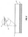
図1について説明すると、本発明により形成された電子デバイス10が示されている。薄膜構成要素12、例えば導体、薄膜トランジスタ、ダイオード、または他の構成要素が、後で説明するように、1つまたは複数の微粒子結合材料および1つまたは複数のプラスチックバインダから構成される、複合材料であるプラスチックなどのフレキシブル基板20上に形成される。複合基板20は、作製処理中ガラスシートなどのキャリア18に付着される。その後の手順により、回路10の作製後、基板20をキャリア18から分離してもよい。電気絶縁および平坦化または平滑さを生じさせるために、ならびに薄膜デバイスを形成するために適した表面を与えるために、1つまたは複数の層14を形成させてもよい。1つの実施形態では、層14は、表面を密閉および絶縁し、薄膜堆積を可能にするために使用される窒化ケイ素である。別の実施形態では、ベンゾシクロブテン(BCB)またはスピンオンガラス(spun−on glass)(SOG)の補足層を平坦化のために使用する。このように使用する場合、層14は従来、ある型の平坦化層と呼ばれる。 Referring to FIG. 1, an
本発明はまた、プラスチックバインダの、基板の少なくとも1つの表面に適用される微粒子材料およびキャリア材料との共最適化、ならびにデバイス層をフレキシブル基板に接着させ、基板内の応力を最小に抑えるためのプロセスに関する。 The present invention also provides for co-optimization of a plastic binder with a particulate material and a carrier material applied to at least one surface of a substrate, and for adhering a device layer to a flexible substrate to minimize stress in the substrate. About the process.
用語が本記載で使用されるように、「プラスチック」は高いポリマー含量を有し、通常、他の成分、例えば硬化剤、フィラー、強化剤、着色剤および可塑剤と組み合わせてもよいポリマー合成樹脂から製造される材料を示す。「樹脂」は合成または天然ポリマーである。プラスチックはその完成した状態では固体であり、完成物品にするための製造または処理中のいくつかの段階では、フローにより成形することができる。プラスチックは典型的には、溶媒が適した速度で蒸発する硬化プロセスを用いて形成させる。プラスチックは熱可塑性材料および熱硬化性材料を含む。 As the term is used in this description, “plastic” has a high polymer content and is usually a polymer synthetic resin that may be combined with other ingredients such as curing agents, fillers, reinforcing agents, colorants and plasticizers. The material manufactured from is shown. A “resin” is a synthetic or natural polymer. Plastic is solid in its finished state and can be molded by flow at some stage during manufacture or processing to make a finished article. Plastics are typically formed using a curing process in which the solvent evaporates at a suitable rate. Plastic includes thermoplastic materials and thermosetting materials.
「フレキシブル」という用語は一般に、約1mmより薄く、プラスチックの弾性係数E、典型的には約100,000〜500,000psiを示すシート材料を示す。 The term “flexible” generally refers to a sheet material that is less than about 1 mm and exhibits an elastic modulus E of plastic, typically about 100,000 to 500,000 psi.
図1に示した電子デバイス10の作製をサポートするために、基板20は適したプラスチックバインダを含み、その表面近くまたはその表面上で含浸させた微粒子材料により調整される独特の調合物を有する。図2について説明すると、1つの実施形態に対する複合基板20の構造配列が拡大視で示されている。微粒子材料16が基板20の基本プラスチック組成物に添加され、プラスチック組成物は微粒子に対しバインダとして機能する。微粒子材料16は、層14への結合を可能にし、そのため層14が絶縁、不動態化、または平滑化を生じさせることができるように、かつプラスチック材料自体のCTEを改善するように適当に選択された、いくつかの型の固体微粒子である。表面近くに微粒子材料16を添加すると、以前は薄膜堆積に適合しなかったPEFEなどの基板上にTFTおよび他の薄膜デバイスを今や作製することができる。このように、基板20の表面のこの調整により、フレキシブル基板上での電子デバイスおよびそれらの関連する連絡配線ならびに他の構成要素の作製が可能になる。複合基板20は、このようにして作製されると、高温に耐えることができ、TFT形成に必要とされる様々な型のエッチャントおよびプロセスに対し回復性が高い。 To support the fabrication of the
<プラスチック材料>
後で説明するように、適当な微粒子材料16をプラスチックに添加することにより、フレキシブル基板のために使用されるプラスチック材料のリストを拡大することができる。例示的なバインダプラスチック材料としては、熱安定ポリエチレンテレフタレート(HS−PET)が挙げられるが、これに限定されない。多くの他のプラスチック基板、例えば、ポリエチレンナフタレート(PEN)、ポリカーボネート(PC)、ポリアリーレート(PAR)、ポリエーテルイミド(PEI)、ポリエーテルスルホン(PES)、ポリイミド(PI)、テフロン(登録商標)ポリ(ペルフルオロ−アルボキシ)フルオロポリマー(PFA)、ポリ(エーテルエーテルケトン)(PEEK)、ポリ(エーテルケトン)(PEK)、ポリ(エチレンテトラフルオロエチレン)フルオロポリマー(PETFE)、およびポリ(メチルメタクリレート)ならびに様々なアクリレート/メタクリレートコポリマー(PMMA)をバインダとして使用することができる。バインダとして使用するために適したプラスチックとしては、様々な環状ポリオレフィン類、JSR社により作製されたアートン、ゼオンケミカルズ・エル・ピーにより製造されたゼオノアおよびセラニーズ・エー・ジーにより作製されたトパスが挙げられる。他の低温プラスチック基板もまた使用することができ、アウジモント・ユー・エス・エー社からハーラーとして販売されているエチレン−クロロトリフルオロエチレン(E−CTFE)、デュポン社により商標名テフゼルで販売されているエチレン−テトラフルオロエチレン(E−TFE)、ポリ−テトラフルオロ−エチレン(PTFE)、ガラス繊維強化プラスチック(FEP)および高密度ポリエチレン(HDPE)が挙げられる。いくつかの用途では、透明プラスチックは非常に利点があるであろう。<Plastic material>
As will be explained later, by adding the appropriate
微粒子材料16を添加すると、あるこれらのプラスチック基板は、少なくとも200℃までのより高い処理温度に耐えることができ、中には、損傷無しで、300℃またはそれより高い温度に耐えることができるものもある。 With the addition of
特に興味深いプラスチックバインダ材料としては、前に述べたようなポリイミド、およびデュポン社により市販されている、テフロン(登録商標)として商業的に知られている、ポリテトラフルオロエチレン(PTFE)またはポリ(ペルフルオロ−アルボキシ)フルオロポリマー(PFA)が挙げられる。前に述べたように、従来形成されているようなポリイミドもPTFEも、TFT堆積のための基板として本質的によく適していないが、多くの異なる表面処理が限定された成功を示している。しかしながら、これらの材料を本発明に従い処理すると、TFT回路を支持するのに非常に有利な特性を有するフレキシブル基板を提供することができる。 Particularly interesting plastic binder materials include polyimide as previously described, and polytetrafluoroethylene (PTFE) or poly (perfluoro), commercially known as Teflon®, marketed by DuPont. -Alboxy) fluoropolymer (PFA). As previously mentioned, neither polyimides nor PTFE as conventionally formed are inherently well suited as substrates for TFT deposition, but many different surface treatments have shown limited success. However, processing these materials in accordance with the present invention can provide a flexible substrate having very advantageous properties for supporting TFT circuits.
さらに別の実施形態では、1つまたは複数のこれらのプラスチック材料を含む組成物が好ましい解決策となる可能性がある。例えば、ポリイミドをポリテトラフルオロエチレン(PTFE)またはポリ(ペルフルオロ−アルボキシ)フルオロポリマー(PFA)と組み合わせることが、両方のプラスチックのより有利な特性を得るために、好都合である可能性がある。 In yet another embodiment, a composition comprising one or more of these plastic materials may be a preferred solution. For example, combining polyimide with polytetrafluoroethylene (PTFE) or poly (perfluoro-alkoxy) fluoropolymer (PFA) may be advantageous in order to obtain more advantageous properties of both plastics.
<微粒子材料の特性>
適した微粒子材料16としては、スピンオンガラスを含むガラス、炭素、繊維、金属繊維、およびプラスチックが挙げられる。微粒子材料16はまた、織物材料または繊維、例えば織物ガラス繊維などとすることができる。微粒子材料16は様々な構造特性および形状を有する可能性がある。微粒子材料16は、大体球形の粒子、基板の厚さより小さな、またはそれを超える寸法の板状晶であってもよい。微粒子材料16は細長い形状とすることができ、例えば、ワイヤ、ロッド、または繊維が含まれる。セラミックフィラーまたは他の誘電材料を微粒子材料16として使用することができる。<Characteristics of particulate material>
Suitable
プラスチックバインダ材料内の微粒子材料16の角度的配向もまた変動させることができる。例えば、細長い微粒子材料16は単一方向でまたは交互の向きの層内で次元的に配列させることができ、または1つの面内で2つまたはそれ以上の軸に沿って配列させることができる。微粒子材料16は基板20の表面に対し特定の方向またはパターンで配向させることができ、これは、異方性の光、電子、熱、磁気、化学または物理特性に影響する可能性がある。単なる一例として、バインダ内の微粒子材料16の繊維は、垂直に配向させることができ、垂直方向に光または熱を導くことができる。また、横方向に配向させた光ファイバを使用して、別の方向に複合基板20を通して光を導くことができる。 The angular orientation of the
多くの特性、例えば下記を改善するために、無機材料を微粒子材料16として導入することができる:
・選択された光学特性、例えば色または光散乱;
・選択された電子特性、例えば伝導率または静電遮蔽のための炭素充填;
・選択された熱特性、例えば熱伝導性を改善するための金属粒子充填;
・選択された磁気特性、磁性付与またはデータ保存のために使用される強磁性材料を含む磁性材料を用いて;
・化学特性、例えばプロセス化学に対する耐性など、または物理特性、例えばCTE、引張強さ、圧縮強度、モジュラス、またはフレキシビリティ;または
・放射特性、例えば放射線遮蔽またはエネルギー選択的X線透過または吸収。Inorganic materials can be introduced as
Selected optical properties, such as color or light scattering;
Selected electronic properties such as carbon filling for conductivity or electrostatic shielding;
-Metal particle packing to improve selected thermal properties, eg thermal conductivity;
With magnetic materials, including ferromagnetic materials used for selected magnetic properties, magnetizing or data storage;
Chemical properties such as resistance to process chemistry, or physical properties such as CTE, tensile strength, compressive strength, modulus, or flexibility; or radiation properties such as radiation shielding or energy selective X-ray transmission or absorption.
本発明による、微粒子材料16のプラスチックバインダ材料との組み合わせの1つの重要な結果は、改善された熱膨張係数(CTE)に関する。複合基板のCTEは、プラスチックバインダのCTEに近似するよりも、TFTデバイスのためのデバイス層のCTEにより密接に近似することが見出されている。このように、複合基板のCTEは、デバイス作製のために従来使用されているガラスまたはシリコンキャリア18のCTEにより密接に近似する。結果として、デバイス作製中、デバイス層に導入される応力はより低くなり、デバイス性能、寸法安定性、および信頼性が改善される。これによって、TFT装置が基板から分離される層間剥離の可能性も最小に抑えられる。 One important result of the combination of
微粒子材料16としてガラスまたはセラミックなどの無機微粒子材料を添加するとまた、下記を含む多くの追加の利点が得られる:
・微粒子表面がプラスチックバインダだけの場合よりも良好な接着を生じるので、TFT層の接着が改善される。
・デバイス作製のための改善された温度制限:微粒子材料の使用により、寸法安定性の喪失前の温度制限が増加し、これにより、より高い温度でデバイス作製が可能になる。
・材料のいくつかの組み合わせでは、微粒子材料は基板の誘電定数を減少させる可能性があり、これにより都合よく、容量が減少する。The addition of inorganic particulate material such as glass or ceramic as
-Adhesion of the TFT layer is improved because the fine particle surface produces better adhesion than when only the plastic binder is used.
Improved temperature limit for device fabrication: The use of particulate material increases the temperature limit prior to loss of dimensional stability, which allows device fabrication at higher temperatures.
• For some combinations of materials, the particulate material can reduce the dielectric constant of the substrate, which advantageously reduces capacitance.
透明微粒子材料16は多くの用途で好都合である。光挙動が重要な場合、微粒子材料16はプラスチックバインダ材料の屈折率n2に対する屈折率n1に基づき選択されてもよい。それらの個々の屈折率n1およびn2が一致する、または非常に近くで一致する場合、光学散乱は最小に抑えることができる。屈折率n1およびn2がより近く一致するほど、散乱が少なくなる。また、光学散乱が望ましい場合があり、そのような場合、屈折率n1およびn2の間の差が、例えば約0.1を超える値だけ、増加し、それに応じて散乱が増加する。不透明または反射材料を使用することができる。光吸収着色剤をプラスチック材料に、ならびに微粒子材料16に添加し、迷光を吸収し、色を加え、または入射もしくは出射光に対するフィルタを提供することができる。同様に、平坦化層14は着色剤を有することができる。Transparent
[実施例1]
1つの実施形態では、複合基板20のために使用される材料はPTFE織物ガラス繊維積層板、例えば、カリフォルニア州ランチョ・クカモンガから入手可能なジクラッド(DiClad)522、527シリーズ由来の材料である。温度応力下で寸法的に安定な、PTFE織物ガラス繊維積層板が、例えばプリント回路基板(PCB)のために使用されてきたが、この目的のために使用される場合、銅層、典型的には電着銅層が用意される。本発明のフレキシブル基板20では、銅めっきは使用されない。フレキシブル基板20として使用するためには、PTFE織物ガラス繊維積層板に対する理想的な厚さは約25μm〜約3000μmの範囲である。[Example 1]
In one embodiment, the material used for the
この基板を前提として、TFT作製処理は下記の通りである:
1.キャリア18上への載置。フレキシブル基板は最初にガラスキャリア18上に積層させる。これは、基板20をキャリア18上に配置し、熱または圧力を印加しPTFE材料の流れ温度(Tg)、約300℃を達成することによりこの組み合わせを処理することにより実施される。PTFE材料は軟化し、再流動し、キャリア18表面に接着する。Given this substrate, the TFT fabrication process is as follows:
1. Place on
2.表面処理。この次の工程は基板20の表面を調整または処理し、層14の接着を可能にする、適した下地を与える。1つの実施形態では、層14は平坦化層である。層14はまた、別の予備材料としてもよく、または薄膜電子デバイス自体を形成する際に使用される材料を含んでもよい。この処理は、微粒子材料16を基板表面に埋め込むことにより実施される。図2に示されるように、微粒子材料16を基板20表面に最も近くで添加することが好都合である。微粒子材料16は、例えば、圧延、またはダスティング(dusting)を含む多くの方法により表面に適用することができる。微粒子材料16はまた、インクジェット堆積、印刷、中間材料からの転写、例えば、溶媒中でのドクターブレードスカイビング技術を用いた塗布、散布、または他の方法により適用することができる。プラスチック材料は加熱することができ、微粒子材料16の埋め込みが促進される。また、微粒子材料16を硬化プロセス中にバインダプラスチック材料に添加することができる。表面処理のためのさらに別の方法を後で記載する。 2. surface treatment. This next step conditions or treats the surface of the
3.平坦化。TFT堆積のための所望の表面粗さは、いくかの適用では0.2〜0.3μm未満のピーク・ツウ・ピーク(peak−to−peak)のオーダーとすることができる。これを達成するために、スピンオンガラス(SOG)が堆積される。この基板を適用するために、コロイドシリカ粒子を含む溶媒のゾルを基板20表面に適用する。ゾル材料を硬化させるために300〜400℃の温度を適用し、溶媒を除去し、ゲル残留物を残し、これはそれ自体加熱すると、約3〜5の間の誘電定数εを有するSiO2膜に変換され、TFT堆積前に必要とされる絶縁および平坦化を生じる。別の平坦化材料は後で説明する。3. Flattening. The desired surface roughness for TFT deposition can be on the order of peak-to-peak less than 0.2-0.3 μm for some applications. To accomplish this, spin-on glass (SOG) is deposited. In order to apply this substrate, a solvent sol containing colloidal silica particles is applied to the surface of the
CTE一致および応答の改善の他に、本発明の方法はTFT構成要素を改善された様式で基板20の表面に結合させる。表面近くに存在する、または複合基板20の表面からわずかに外に向かって実に延在する微粒子材料16は、絶縁窒化ケイ素または酸化ケイ素層である可能性のある、層14のための結合表面領域を生じる。微粒子材料16が存在しないと、これらのシリコン化合物は表面に接着することができず、機能するTFTデバイスまたは他の型の電子デバイスがその上に作製される可能性が著しく妨げられる。 In addition to CTE matching and improved response, the method of the present invention couples TFT components to the surface of
4.電気絶縁層の形成。必要に応じて用いてもよい、基板の表面を調整するための最終表面準備工程として、電気絶縁層を、平坦化層の上面に堆積させる。適した絶縁層材料は、SiO2、SiNx、SiON、またはこれらの材料のいくつかの組み合わせとすることができる。これは典型的には、約0.5〜1.5μmの範囲である。4). Formation of electrical insulation layer. As a final surface preparation step for adjusting the surface of the substrate, which may be used as necessary, an electrical insulating layer is deposited on the upper surface of the planarization layer. Suitable insulating layer materialcan be SiO2, SiN x, SiON, or with some combination of these materials, to. This is typically in the range of about 0.5 to 1.5 μm.
5.TFT要素の形成。フレキシブル基板20表面の準備後、TFT要素の構築(lay−down)を始めることができる。これには典型的には、薄膜半導体材料層の基板上への堆積、その後、半導体材料の一部の選択的除去によるパターンの形成が必要とされる。この手順は、ゲート、ソース、およびドレイン構成要素ならびに他の支持層の構築のための構成要素作製技術分野において周知のプロセスを使用する。 5). Formation of TFT elements. After the surface of the
6.キャリア18からの層剥離。これには、基板プラスチック材料の流れ温度付近の温度での熱の適用が必要である可能性がある。これにより基板20がキャリア18から分離される。分離されると直ちに、基板20を他の何らかの表面に積層させることができ、または冷却させることができる。 6). Delamination from
実施例1の方法は、特定の基板および構成要素型のために改良することができる。例えば、他のスピンコート誘電処理を代わりに使用することができる。 The method of Example 1 can be modified for specific substrates and component types. For example, other spin coat dielectric processes can be used instead.
[実施例2]
この次の実施例は、複合基板20を構築するために必要とされ得る追加の工程を検討する。基本的な工程は下記の通りである:
1.プラスチックをその溶融温度Tgまで加熱する。[Example 2]
This next example considers additional steps that may be required to construct the
1. The plastic is heated to its melting temperature Tg.
2.溶融したプラスチックに微粒子材料16をフィラーとして添加する。改善された接着のために、微粒子材料16は、基板20の表面上または表面近くに堆積されると最もよく機能する。しかしながら、改善されたCTEのためには、プラスチック材料全体に混合された粒子のより一般的な分布が好ましい。ほとんどの場合、基板20表面近くで、より濃度の濃い微粒子材料16、または微粒子材料16の露出した部分を有することが好ましい。このように、この工程では微粒子材料16と溶融プラスチックバインダとのいくらかの混合が必要である。 2. The
3.キャリア18上への載置。フレキシブル基板は最初にガラスキャリア18上に積層される。これは、基板20をキャリア18上に配置し、熱および圧力を印加してPTFE材料の流れ温度(Tg)、約300℃を達成することによりこの組み合わせを処理することにより実施される。PTFE材料は軟化し、再流動化し、キャリア18の表面に接着する。 3. Place on
4.平坦化。TFT堆積のための望ましい表面粗さは、いくつかの用途で0.2〜0.3μm未満のオーダーのピーク・ツウ・ピークとすることができる。これを達成するために、スピンオンガラス(SOG)を堆積させる。この基板を適用するために、コロイドシリカ粒子を含む溶媒のゾルを基板20表面に塗布する。300〜400℃の温度を適用しゾル材料を硬化させ、溶媒を除去し、ゲル残留物を残し、これはそれ自体加熱すると、約3〜5の間の誘電定数εを有するSiO2膜に変換され、TFT堆積前に必要とされる絶縁および平坦化を生じる。別の平坦化材料は後で記載する。4). Flattening. The desired surface roughness for TFT deposition can be peak-to-peak on the order of 0.2 to less than 0.3 μm for some applications. To achieve this, spin-on glass (SOG) is deposited. In order to apply this substrate, a solvent sol containing colloidal silica particles is applied to the surface of the
5.電気絶縁層の形成。必要に応じて用いてもよい、基板の表面を調整するための最終表面前準備工程として、電気絶縁層を平坦化層の上面に堆積させる。適した絶縁層材料はSiO2、SiNx、SiON、またはこれらの材料のいくつかの組み合わせとすることができる。これは典型的には約0.5〜1.5μmの範囲である。5. Formation of electrical insulation layer. As a final surface preparation step for adjusting the surface of the substrate, which may be used as necessary, an electrical insulating layer is deposited on the upper surface of the planarization layer. Suitable insulating layer material may be some combination ofSiO2, SiN x, SiON, or these materials. This is typically in the range of about 0.5 to 1.5 μm.
6.TFT要素の形成。フレキシブル基板20表面の準備後、TFT要素の構築を始めることができる。この手順はゲート、ソースおよびドレイン厚生要素および他の支持層の構築のための構成要素作製分野において周知である方法を使用する。TFT作製の一部として、半導体材料を堆積させ、その後、半導体材料の一部を選択的に除去することによりパターンを形成させる。 6). Formation of TFT elements. After preparation of the surface of the
7.キャリア18からの層剥離。これには、基板プラスチック材料の流れ温度付近の温度での熱の適用が必要である可能性がある。これにより基板20がキャリア18から分離される。分離されると直ちに、基板20を他の何らかの表面に積層させることができ、または冷却させることができる。別の層剥離法もまた使用することができる。 7. Delamination from
[実子例3]
別の実施形態では、基板20はポリイミドまたはポリイミド組成物およびバインダから、下記工程を使用して形成される:
1.未硬化プラスチックバインダ材料を適したキャリア上にコートする。ここで、部分的に硬化させたポリイミドをキャリア上にコートする。ディップスカイビング、スピンオン塗布、または押出を含む任意の適した塗布法を使用することができる。[Example 3]
In another embodiment, the
1. Coat uncured plastic binder material onto a suitable carrier. Here, a partially cured polyimide is coated on the carrier. Any suitable coating method can be used including dip skiving, spin-on coating, or extrusion.
2.硬化プロセスが大体完了するまで、未硬化プラスチック材料を硬化する。 2. The uncured plastic material is cured until the curing process is largely complete.
3.硬化サイクルの約80%が完了すると、微粒子材料16を基板20表面に添加する。ここで、微粒子材料16は表面上に散布され、均一なコーティングが与えられる。 3. When about 80% of the cure cycle is complete, the
4.硬化プロセスを完了し、残った溶媒を焼いて除去する。 4). Complete the curing process and bake off any remaining solvent.
5.平坦化。TFT堆積のための所望の表面粗さは、いくつかの用途で0.2〜0.3μm未満のオーダーのピーク・ツウ・ピークとすることができる。これを達成するために、スピンオンガラス(SOG)を堆積させる。この基板を適用するために、コロイドシリカ粒子を含む溶媒のゾルを基板20表面に塗布する。300〜400℃の温度を適用しゾル材料を硬化させ、溶媒を除去し、ゲル残留物を残し、これはそれ自体加熱すると、約3〜5の間の誘電定数εを有するSiO2膜に変換され、TFT堆積前に必要とされる絶縁および平坦化を生じる。別の平坦化材料は後で記載する。5. Flattening. The desired surface roughness for TFT deposition can be peak-to-peak on the order of 0.2 to less than 0.3 μm for some applications. To achieve this, spin-on glass (SOG) is deposited. In order to apply this substrate, a solvent sol containing colloidal silica particles is applied to the surface of the
6.電気絶縁層の形成。必要に応じて用いてもよい、基板の表面を調整するための最終表面前準備工程として、電気絶縁層を平坦化層の上面に堆積させる。適した絶縁層材料はSiO2、SiNx、SiON、またはこれらの材料のいくつかの組み合わせとすることができる。これは典型的には約0.5〜1.5μmの範囲である。6). Formation of electrical insulation layer. As a final surface pre-preparation step for adjusting the surface of the substrate, which may be used as necessary, an electrical insulating layer is deposited on the upper surface of the planarization layer. Suitable insulating layer material may be some combination ofSiO2, SiN x, SiON, or these materials. This is typically in the range of about 0.5 to 1.5 μm.
7.TFT要素の形成。フレキシブル基板20表面の準備後、TFT要素の構築を始めることができる。この手順はゲート、ソースおよびドレイン構成要素および他の支持層の構築のための構成要素作製分野において周知である方法を使用する。TFT作製の一部として、半導体材料を堆積させ、その後、半導体材料の一部を選択的に除去することによりパターンを形成させる。 7. Formation of TFT elements. After preparation of the surface of the
8.キャリア18からの層剥離。これには、基板プラスチック材料の流動温度付近の温度での熱の適用が必要である可能性がある。これにより基板20がキャリア18から分離される。分離されると直ちに、基板20を他の何らかの表面に積層させることができ、または冷却させることができる。別の層剥離法もまた使用することができる。 8). Delamination from
別の実施形態では、微粒子材料16は未硬化プラスチックにフィラーとして添加することができ、実施例2で記載したCTEの利点を有する。 In another embodiment, the
<表面処理法>
層14および薄膜デバイス作製のための他の材料の接着を改善するための基板20の表面の調整は、多くの様式で実施することができる。前に述べたように、本発明の方法は、微粒子材料16の表面が基板20表面上で露出され、これにより接着表面が与えられると、最もよく機能する。基板20内でバインダとして使用されるプラスチック材料の性質のため、微粒子材料16のフィラーが使用されている場合でも、基板20の表面は一般に、高い比率の樹脂量を有する。このように、接着を改善するために微粒子材料16を露出させるには、表面自体に沿ってある割合のプラスチック材料を除去するためのいくつかの方法が必要となる可能性がある。<Surface treatment method>
The conditioning of the surface of the
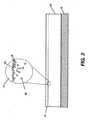
図3の拡大部分は、微粒子材料16を露出させると、表面22がどのように特徴づけられるかを示す。このように表面を調整するための方法は下記を含む:
・多くの適した酸を含む、エッチャント材料を使用するなどの化学的除去
・プラズマエッチング
・コロナ放電処理
・熱の適用
・超臨界二酸化炭素、CO2の使用
・レーザアブレーション
・真空での熱分解The enlarged portion of FIG. 3 shows how the surface 22 is characterized when the
· Including many suitable acid, thermal decomposition of a chemical removal plasma application, supercritical carbon dioxide etch corona discharge treatment, heat, using laser ablation vacuum CO2, such as using an etchant material
プラスチックバインダ材料除去のためのこれらの表面処理法の適用は、表面処理技術分野の当業者によく知られている。微粒子材料16が、基板20の表面上および表面近くで著しく集中しているフィラーとして添加され、または埋め込まれている図1の例示的な実施形態とは異なり、基板20がフィラーとしてプラスチックバインダ内で全体的に事実上均一に混合されている微粒子材料16混合物から構成される場合、これらの表面処理法を使用することができる。前に述べたように、そのような材料の固有の利点はその改善されたCTEである。 The application of these surface treatment methods for plastic binder material removal is well known to those skilled in the surface treatment art. Unlike the exemplary embodiment of FIG. 1, where the
別の実施形態では、PTFEの再流動の利点を使用すると、表面調整に有利である。微粒子材料16はPTFEまたはPTFE組成物の加熱表面に、別の適した材料と共に、そのガラス転移温度Tgのより少し高い温度で振りかける、または散布することができる。PTFE材料を冷却させると、平坦化層または他の層の堆積のために調整された表面が得られる。今述べた調整法を用いる、いくらかの量の処理を使用して、微粒子材料16の堆積後に、基板20の表面を改善してもよい。 In another embodiment, the advantage of PTFE reflow is advantageous for surface conditioning. The
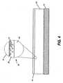
さらに別の実施形態では、図4に示されるように、第1のプラスチック材料がベース基板24として用意される。その後、組成物26をこのベース基板の表面上にコートし、ここで、組成物は少なくとも1つの微粒子材料16と混合されるプラスチックバインダ材料を含む。このように、このプロセスにより、例えば、図4で示されるような平坦化層14、絶縁層、または薄膜電子デバイスのいくつかの部分を形成するために使用される電気活性半導体層であってもよい1つまたは複数の層を堆積させるように適当に処理された表面が与えられる。 In yet another embodiment, a first plastic material is provided as the
<平坦化材料>
スピンオンガラスの他に、下記平坦化材料を異なる実施形態で使用してもよい:
・ベンゾシクロブテン(BCB)。この材料は半導体グレードでなければならず、可動イオンが存在しない。
・アクリル
・テトラエトキシシラン(TEOS)<Planarizing material>
In addition to spin-on glass, the following planarization materials may be used in different embodiments:
Benzocyclobutene (BCB). This material must be semiconductor grade and free of mobile ions.
・ Acrylic tetraethoxysilane (TEOS)
プラスチック基板を使用しようと試みる他の解決策に対し、ガラス、セラミック、または他の適した微粒子はプラスチックバインダのみの場合よりも良好な接着性を与えるので、本発明の方法はTFT層の接着の改善を促進する。微粒子材料16を使用すると、寸法安定性が喪失する前の温度限界が増加し、より高い温度でのデバイス作製が可能になる。 In contrast to other solutions that attempt to use plastic substrates, the method of the present invention provides better adhesion of TFT layers because glass, ceramic, or other suitable particulates give better adhesion than plastic binders alone. Promote improvement. Use of the
本発明の方法は、TFT構成要素を直接フレキシブル基板上に形成することができ、積層などの中間工程が必要ないので、好都合である。この方法は、特に、ウエブ(web)またはロール・ツウ・ロール(roll−to−roll)作製に適しており、この場合、基板シートは第1のロールから解かれ、前に記述したように微粒子材料16を埋め込むことにおり表面調整を受け、さらに処理され、または第2のロールで将来の使用のために巻き戻される。 The method of the present invention is advantageous because TFT components can be formed directly on a flexible substrate and no intermediate steps such as lamination are required. This method is particularly suitable for web or roll-to-roll production, where the substrate sheet is unwound from the first roll and fine particles as previously described. Embedding
様々な型の広範囲の微粒子物質を、微粒子材料16として、または、複数の材料の有利な特性を利用する、使用される微粒子材料の混合物として使用することができる。前に記載したように、電子デバイス作製プロセスにおける様々な点で、プラズマエッチングなどのツールを使用して、別の型の表面調整を使用することができる。基板材料のシートの1つの側または両側を、本発明の方法を用いて処理することができる。エンボス加工を含む様々な方法を、平坦化層14適用およびTFTデバイス形成前に基板20の表面を準備するために使用することができる。基板20または平坦化層14上に形成した構成要素は、1つまたは複数のレンズまたは小レンズなどの屈折構成要素を含む光学要素を含むことができる。小レンズはTFT構成要素と空間的に整合させることができ、入力画素要素または出力画素要素が提供される。 A wide variety of particulate materials of various types can be used as
基板20上に形成された電子デバイスを使用して、多くの異なる型の構成要素のいずれかへ、またはそれらから信号を与えることができ、画像表示画素またはイメージセンシング画素に対し特別な用途を有する。例えば、基板20表面上に形成された電子デバイスは、例えば、対応する液晶画素、発光ダイオード画素、またはディスプレイ用の有機発光ダイオード画素と結合させることができる。イメージセンシングでは、基板20表面上に形成された電子デバイスは、刺激可能な蛍光体画素と、または生物学的検出器を含む別の型のセンサ画素と結合させることができる。 The electronic device formed on the
本発明はまた、底層がキャリアに関連する特性(例えばキャリアへの接着特性)に対し最適化され、最上層が電子デバイスに関連する特性(例えばデバイス層への接着)に対し最適化され、中間層が選択された特性、例えば、光学、電子、熱、磁気または化学特性を達成するように最適化された多層基板に関する。 The present invention also optimizes the bottom layer for properties related to the carrier (eg, adhesion properties to the carrier), and the top layer is optimized for properties related to the electronic device (eg, adhesion to the device layer). It relates to a multilayer substrate in which the layers are optimized to achieve selected properties, for example optical, electronic, thermal, magnetic or chemical properties.
このように、基板上で電子デバイスを作製するための装置および方法が提供される。 Thus, an apparatus and method for making an electronic device on a substrate is provided.
10 電子デバイス、12 薄膜構成要素、14 層、16 微粒子材料、18 キャリア、20 基板、22 表面、24 ベース基板、26 組成物。 10 electronic devices, 12 thin film components, 14 layers, 16 particulate materials, 18 carriers, 20 substrates, 22 surfaces, 24 base substrates, 26 compositions.
Claims (54)
Translated fromJapanesea)少なくとも1つのプラスチック材料を含む基板を用意する工程と、
b)微粒子材料を前記基板の少なくとも1つの表面内に埋め込む工程と、
c)前記微粒子材料を有する前記表面上で薄膜電子デバイスを形成する工程と、
を含む、方法。An electronic device manufacturing method comprising:
a) providing a substrate comprising at least one plastic material;
b) embedding a particulate material in at least one surface of the substrate;
c) forming a thin film electronic device on the surface having the particulate material;
Including a method.
e)前記埋め込まれた微粒子材料を有する前記第2の表面上に薄膜電子デバイスを形成する工程と、
をさらに含む、請求項1記載の方法。d) embedding the particulate material in the second surface of the substrate;
e) forming a thin film electronic device on the second surface having the embedded particulate material;
The method of claim 1, further comprising:
a)少なくとも1つのプラスチック材料を含む基板を用意する工程と、
b)微粒子材料を前記基板の少なくとも1つの表面内に埋め込む工程と、
c)前記埋め込まれた微粒子材料を有する前記基板表面に平坦化材料を適用し、これにより平坦化層を形成する工程と、
d)前記微粒子材料を有する前記表面上で薄膜電子デバイスを形成する工程と、
を含む、方法。An electronic device manufacturing method comprising:
a) providing a substrate comprising at least one plastic material;
b) embedding a particulate material in at least one surface of the substrate;
c) applying a planarization material to the substrate surface having the embedded particulate material, thereby forming a planarization layer;
d) forming a thin film electronic device on the surface having the particulate material;
Including a method.
a)ベース基板として少なくとも1つのプラスチック材料を含む基板を用意する工程と、
b)前記ベース基板の少なくとも1つの表面上に複合材料をコートし、これにより少なくとも1つのコート表面を形成する工程であって、前記複合材料が、少なくとも1つのプラスチックバインダ材料と少なくとも1つの微粒子材料を含む、工程と、
c)前記少なくとも1つのコート表面上で薄膜電子デバイスを形成する工程と、
を含む、方法。An electronic device manufacturing method comprising:
a) providing a substrate including at least one plastic material as a base substrate;
b) coating a composite material on at least one surface of the base substrate, thereby forming at least one coated surface, the composite material comprising at least one plastic binder material and at least one particulate material Including a process,
c) forming a thin film electronic device on the at least one coat surface;
Including a method.
a)少なくとも1つのプラスチック材料と少なくとも1つの微粒子材料を含む基板を用意する工程と、
b)前記基板の少なくとも1つの表面を調整し、その表面での微粒子材料のプラスチック材料に対する比率を増加させる工程と、
c)前記少なくとも1つの調整表面上で薄膜電子デバイスを形成する工程と、
を含む、方法。An electronic device manufacturing method comprising:
a) providing a substrate comprising at least one plastic material and at least one particulate material;
b) adjusting at least one surface of the substrate to increase the ratio of particulate material to plastic material on the surface;
c) forming a thin film electronic device on the at least one conditioning surface;
Including a method.
a)ポリテトラフルオロエチレン(PTFE)と、少なくとも1つの微粒子材料を含む基板を用意する工程と、
b)前記基板の少なくとも1つの表面上で薄膜電子デバイスを形成する工程と、
を含む、方法。An electronic device manufacturing method comprising:
a) providing a substrate comprising polytetrafluoroethylene (PTFE) and at least one particulate material;
b) forming a thin film electronic device on at least one surface of the substrate;
Including a method.
a)ポリテトラフルオロエチレン(PTFE)と、少なくとも1つの他のプラスチック材料と、少なくとも1つの微粒子材料を含む基板を用意する工程と、
b)前記基板の少なくとも1つの表面上で薄膜電子デバイスを形成する工程と、
を含む、方法。An electronic device manufacturing method comprising:
a) providing a substrate comprising polytetrafluoroethylene (PTFE), at least one other plastic material, and at least one particulate material;
b) forming a thin film electronic device on at least one surface of the substrate;
Including a method.
a)ポリテトラフルオロエチレン(PTFE)と、少なくとも1つの微粒子材料を含む基板を用意する工程と、
b)前記基板をキャリアに積層させる工程と、
c)前記基板上で電子デバイスを形成する工程と、
を含む、方法。An electronic device manufacturing method comprising:
a) providing a substrate comprising polytetrafluoroethylene (PTFE) and at least one particulate material;
b) laminating the substrate on a carrier;
c) forming an electronic device on the substrate;
Including a method.
a)ポリテトラフルオロエチレン(PTFE)と、少なくとも1つの微粒子材料と、少なくとも1つの他のプラスチック材料を含む基板を用意する工程と、
b)前記基板をキャリアに積層させる工程と、
c)前記基板上で電子デバイスを形成する工程と、
d)前記電子デバイスを含む前記基板を前記キャリアから層剥離させる工程と、
を含む、方法。An electronic device manufacturing method comprising:
a) providing a substrate comprising polytetrafluoroethylene (PTFE), at least one particulate material, and at least one other plastic material;
b) laminating the substrate on a carrier;
c) forming an electronic device on the substrate;
d) delaminating the substrate containing the electronic device from the carrier;
Including a method.
a)前記プラスチック材料を、そのガラス転移温度Tg付近の温度まで加熱する工程と、
b)前記微粒子材料を前記プラスチック材料に適用する工程と、
を含む、請求項1記載の方法。The step of embedding the particulate material includes
a) heating the plastic material to a temperature near its glass transition temperature Tg;
b) applying the particulate material to the plastic material;
The method of claim 1 comprising:
a)プラスチック材料と、少なくとも1つの微粒子材料を含む基板を用意する工程と、
b)前記基板をキャリア層上に載置する工程と、
c)薄膜半導体材料を堆積するために前記基板の前記表面を調整する工程と、
d)前記基板上に薄膜半導体材料の層を堆積させる工程と、
e)前記半導体材料の一部を選択的に除去することによりパターンを形成する工程と、
を含む、方法。An electronic device manufacturing method comprising:
a) preparing a substrate comprising a plastic material and at least one particulate material;
b) placing the substrate on a carrier layer;
c) conditioning the surface of the substrate to deposit a thin film semiconductor material;
d) depositing a layer of thin film semiconductor material on the substrate;
e) forming a pattern by selectively removing a portion of the semiconductor material;
Including a method.
をさらに含む、請求項35記載の方法。36. The method of claim 35, further comprising: e) removing the substrate from the carrier layer using heat.
a)少なくとも1つのプラスチック材料を含む基板を用意する工程と、
b)前記基板の少なくとも1つの表面上でパターンを形成する工程と、
c)微粒子材料を前記基板の前記少なくとも1つの表面内に埋め込む工程と、
d)前記埋め込まれた微粒子材料を有する前記基板の前記表面に平坦化材料を適用し、これにより平坦化層を形成する工程と、
e)前記微粒子材料を有する前記表面上で薄膜電子デバイスを形成する工程と、
を含む、方法。An electronic device manufacturing method comprising:
a) providing a substrate comprising at least one plastic material;
b) forming a pattern on at least one surface of the substrate;
c) embedding a particulate material in the at least one surface of the substrate;
d) applying a planarization material to the surface of the substrate having the embedded particulate material, thereby forming a planarization layer;
e) forming a thin film electronic device on the surface having the particulate material;
Including a method.
Applications Claiming Priority (2)
| Application Number | Priority Date | Filing Date | Title |
|---|---|---|---|
| US11/461,080US7678701B2 (en) | 2006-07-31 | 2006-07-31 | Flexible substrate with electronic devices formed thereon |
| PCT/US2007/016085WO2008016479A1 (en) | 2006-07-31 | 2007-07-16 | Flexible substrate with electronic devices formed thereon |
Publications (2)
| Publication Number | Publication Date |
|---|---|
| JP2009545878Atrue JP2009545878A (en) | 2009-12-24 |
| JP2009545878A5 JP2009545878A5 (en) | 2011-09-08 |
Family
ID=38669806
Family Applications (1)
| Application Number | Title | Priority Date | Filing Date |
|---|---|---|---|
| JP2009522771APendingJP2009545878A (en) | 2006-07-31 | 2007-07-16 | Flexible substrate on which electronic devices are formed |
Country Status (5)
| Country | Link |
|---|---|
| US (2) | US7678701B2 (en) |
| EP (1) | EP2047513A1 (en) |
| JP (1) | JP2009545878A (en) |
| TW (1) | TW200814333A (en) |
| WO (1) | WO2008016479A1 (en) |
Cited By (3)
| Publication number | Priority date | Publication date | Assignee | Title |
|---|---|---|---|---|
| JP2010506400A (en)* | 2006-10-03 | 2010-02-25 | イーストマン コダック カンパニー | Flexible substrate with electronic device and trace |
| JP2019121734A (en)* | 2018-01-10 | 2019-07-22 | 株式会社Joled | Semiconductor device and display device |
| KR102084519B1 (en)* | 2019-07-16 | 2020-03-04 | 주식회사 오플렉스 | Backplate film comprising ultraviolet(UV) curable adhesive layer and method for manufacturing organic light emitting display device using the same |
Families Citing this family (19)
| Publication number | Priority date | Publication date | Assignee | Title |
|---|---|---|---|---|
| US7913381B2 (en)* | 2006-10-26 | 2011-03-29 | Carestream Health, Inc. | Metal substrate having electronic devices formed thereon |
| KR101408510B1 (en)* | 2007-05-18 | 2014-06-17 | 삼성전자주식회사 | Flexible substrate for display element and display element using the same |
| US8502259B2 (en) | 2008-01-11 | 2013-08-06 | Industrial Technology Research Institute | Light emitting device |
| US8800138B2 (en)* | 2008-02-08 | 2014-08-12 | Carestream Health, Inc. | Method for conditioning a substrate surface for forming an electronic device thereon and resultant device |
| US20090200543A1 (en)* | 2008-02-08 | 2009-08-13 | Roger Stanley Kerr | Method of forming an electronic device on a substrate supported by a carrier and resultant device |
| US20100032702A1 (en)* | 2008-08-11 | 2010-02-11 | E. I. Du Pont De Nemours And Company | Light-Emitting Diode Housing Comprising Fluoropolymer |
| TWI400673B (en)* | 2009-02-18 | 2013-07-01 | Prime View Int Co Ltd | Flexible display panel and method of manufacturing the same |
| US8074349B2 (en)* | 2009-04-16 | 2011-12-13 | Carestream Health, Inc. | Magnetic hold-down for foil substrate processing |
| GB0909721D0 (en)* | 2009-06-05 | 2009-07-22 | Plastic Logic Ltd | Dielectric seed layer |
| TWI387138B (en)* | 2009-07-10 | 2013-02-21 | Ind Tech Res Inst | Magnetic light eitting device, magnetic light eitting apparatus and semi-conductive nitride template |
| EP2404650A1 (en)* | 2010-07-09 | 2012-01-11 | Bayer MaterialScience AG | Method and device for solid-liquid separation of solid-liquid suspensions |
| US20130188324A1 (en)* | 2010-09-29 | 2013-07-25 | Posco | Method for Manufacturing a Flexible Electronic Device Using a Roll-Shaped Motherboard, Flexible Electronic Device, and Flexible Substrate |
| USRE49869E1 (en)* | 2015-02-10 | 2024-03-12 | iBeam Materials, Inc. | Group-III nitride devices and systems on IBAD-textured substrates |
| KR20160127892A (en)* | 2015-04-27 | 2016-11-07 | 삼성디스플레이 주식회사 | Flexible substrate and display device including the same |
| JP7044802B2 (en) | 2017-04-04 | 2022-03-30 | ダブリュ.エル.ゴア アンド アソシエーツ,ゲゼルシャフト ミット ベシュレンクテル ハフツング | Dielectric complex with reinforced elastomer and integrated electrodes |
| US11212916B2 (en) | 2018-05-08 | 2021-12-28 | W. L. Gore & Associates, Inc. | Flexible printed circuits for dermal applications |
| KR102517008B1 (en) | 2018-05-08 | 2023-03-31 | 더블유.엘. 고어 앤드 어소시에이트스, 인코포레이티드 | Flexible, extensible printed circuits on extensible substrates |
| CN112106452A (en) | 2018-05-08 | 2020-12-18 | W.L.戈尔及同仁股份有限公司 | Flexible and durable printed circuits on stretchable and non-stretchable substrates |
| CN109285462B (en)* | 2018-12-12 | 2021-04-20 | 武汉天马微电子有限公司 | Flexible display panel, manufacturing method thereof and flexible display device |
Citations (8)
| Publication number | Priority date | Publication date | Assignee | Title |
|---|---|---|---|---|
| JP2002108250A (en)* | 2000-09-29 | 2002-04-10 | Sharp Corp | Active matrix drive type self-luminous display device and manufacturing method thereof |
| JP2004140267A (en)* | 2002-10-18 | 2004-05-13 | Semiconductor Energy Lab Co Ltd | Semiconductor device and manufacturing method thereof |
| JP2004515081A (en)* | 2000-11-30 | 2004-05-20 | インフィネオン テクノロジーズ アクチェンゲゼルシャフト | Substrate having semiconductor layer, electronic device, electronic circuit, printable composition and method of making |
| JP2004200365A (en)* | 2002-12-18 | 2004-07-15 | Konica Minolta Holdings Inc | Organic thin film transistor element |
| US20050163968A1 (en)* | 2004-01-20 | 2005-07-28 | Hanket Gregory M. | Microfiller-reinforced polymer film |
| JP2005210081A (en)* | 2003-12-02 | 2005-08-04 | Semiconductor Energy Lab Co Ltd | Electronic appliance, and semiconductor apparatus and formation method therefor |
| JP2006013480A (en)* | 2004-05-28 | 2006-01-12 | Semiconductor Energy Lab Co Ltd | Thin film transistor, display, methods of manufacturing them, and television device |
| JP2006100662A (en)* | 2004-09-30 | 2006-04-13 | Sony Corp | Method of manufacturing thin film semiconductor device |
Family Cites Families (30)
| Publication number | Priority date | Publication date | Assignee | Title |
|---|---|---|---|---|
| US5237436A (en)* | 1990-12-14 | 1993-08-17 | North American Philips Corporation | Active matrix electro-optic display device with light shielding layer and projection and color employing same |
| US5891552A (en)* | 1996-01-04 | 1999-04-06 | Mobil Oil Corporation | Printed plastic films and method of thermal transfer printing |
| US5817550A (en)* | 1996-03-05 | 1998-10-06 | Regents Of The University Of California | Method for formation of thin film transistors on plastic substrates |
| US6492026B1 (en)* | 2000-04-20 | 2002-12-10 | Battelle Memorial Institute | Smoothing and barrier layers on high Tg substrates |
| AU2001269929B2 (en)* | 2000-06-19 | 2005-11-03 | Caliper Life Sciences, Inc. | Methods and devices for enhancing bonded substrate yields and regulating temperature |
| US6762124B2 (en)* | 2001-02-14 | 2004-07-13 | Avery Dennison Corporation | Method for patterning a multilayered conductor/substrate structure |
| US7535624B2 (en)* | 2001-07-09 | 2009-05-19 | E Ink Corporation | Electro-optic display and materials for use therein |
| US7110163B2 (en)* | 2001-07-09 | 2006-09-19 | E Ink Corporation | Electro-optic display and lamination adhesive for use therein |
| JP2003045234A (en)* | 2001-07-26 | 2003-02-14 | Dainippon Printing Co Ltd | Transparent conductive film |
| TWI308231B (en)* | 2001-08-28 | 2009-04-01 | Sipix Imaging Inc | Electrophoretic display |
| US20030193796A1 (en)* | 2002-04-15 | 2003-10-16 | Heeks Stephen K. | Light-emitting devices |
| US7223672B2 (en)* | 2002-04-24 | 2007-05-29 | E Ink Corporation | Processes for forming backplanes for electro-optic displays |
| EP1362682A1 (en) | 2002-05-13 | 2003-11-19 | ZBD Displays Ltd, | Method and apparatus for liquid crystal alignment |
| TWI330269B (en)* | 2002-12-27 | 2010-09-11 | Semiconductor Energy Lab | Separating method |
| US20050216075A1 (en)* | 2003-04-08 | 2005-09-29 | Xingwu Wang | Materials and devices of enhanced electromagnetic transparency |
| JP4233433B2 (en)* | 2003-11-06 | 2009-03-04 | シャープ株式会社 | Manufacturing method of display device |
| US8314203B2 (en)* | 2003-12-26 | 2012-11-20 | Toyo Boseki Kabushiki Kaisha | Polyimide film |
| US8053171B2 (en)* | 2004-01-16 | 2011-11-08 | Semiconductor Energy Laboratory Co., Ltd. | Substrate having film pattern and manufacturing method of the same, manufacturing method of semiconductor device, liquid crystal television, and EL television |
| EP1737053B1 (en)* | 2004-03-25 | 2012-02-29 | National Institute of Advanced Industrial Science and Technology | Thermoelectric conversion element and thermoelectric conversion module |
| EP1791185A1 (en)* | 2004-07-27 | 2007-05-30 | Quantum 14 KK | Light-emitting element, light-emitting device and information display |
| US7582904B2 (en)* | 2004-11-26 | 2009-09-01 | Semiconductor Energy Laboratory Co., Ltd. | Semiconductor device, display device and method for manufacturing thereof, and television device |
| US20060180890A1 (en)* | 2005-01-18 | 2006-08-17 | Naugler W E Jr | Top emission flat panel display with sensor feedback stabilization |
| TWI408734B (en)* | 2005-04-28 | 2013-09-11 | Semiconductor Energy Lab | Semiconductor device and method of manufacturing same |
| TWI402935B (en)* | 2005-05-17 | 2013-07-21 | Koninkl Philips Electronics Nv | Color active matrix display |
| WO2006137203A1 (en)* | 2005-06-20 | 2006-12-28 | Matsushita Electric Industrial Co., Ltd. | Method for manufacturing film-electrode bonded body |
| KR101102152B1 (en)* | 2005-06-28 | 2012-01-02 | 삼성전자주식회사 | Method for manufacturing organic thin film transistor and organic thin film transistor produced by |
| US20070002199A1 (en)* | 2005-06-30 | 2007-01-04 | Semiconductor Energy Laboratory Co., Ltd. | Liquid crystal display device and method for manufacturing the same |
| US20070007579A1 (en)* | 2005-07-11 | 2007-01-11 | Matrix Semiconductor, Inc. | Memory cell comprising a thin film three-terminal switching device having a metal source and /or drain region |
| GB2430547A (en) | 2005-09-20 | 2007-03-28 | Seiko Epson Corp | A method of producing a substrate having areas of different hydrophilicity and/or oleophilicity on the same surface |
| US7235736B1 (en)* | 2006-03-18 | 2007-06-26 | Solyndra, Inc. | Monolithic integration of cylindrical solar cells |
- 2006
- 2006-07-31USUS11/461,080patent/US7678701B2/ennot_activeExpired - Fee Related
- 2007
- 2007-07-16JPJP2009522771Apatent/JP2009545878A/enactivePending
- 2007-07-16EPEP07796875Apatent/EP2047513A1/ennot_activeWithdrawn
- 2007-07-16WOPCT/US2007/016085patent/WO2008016479A1/enactiveApplication Filing
- 2007-07-30TWTW096127807Apatent/TW200814333A/enunknown
- 2010
- 2010-02-01USUS12/697,522patent/US7964507B2/ennot_activeExpired - Fee Related
Patent Citations (8)
| Publication number | Priority date | Publication date | Assignee | Title |
|---|---|---|---|---|
| JP2002108250A (en)* | 2000-09-29 | 2002-04-10 | Sharp Corp | Active matrix drive type self-luminous display device and manufacturing method thereof |
| JP2004515081A (en)* | 2000-11-30 | 2004-05-20 | インフィネオン テクノロジーズ アクチェンゲゼルシャフト | Substrate having semiconductor layer, electronic device, electronic circuit, printable composition and method of making |
| JP2004140267A (en)* | 2002-10-18 | 2004-05-13 | Semiconductor Energy Lab Co Ltd | Semiconductor device and manufacturing method thereof |
| JP2004200365A (en)* | 2002-12-18 | 2004-07-15 | Konica Minolta Holdings Inc | Organic thin film transistor element |
| JP2005210081A (en)* | 2003-12-02 | 2005-08-04 | Semiconductor Energy Lab Co Ltd | Electronic appliance, and semiconductor apparatus and formation method therefor |
| US20050163968A1 (en)* | 2004-01-20 | 2005-07-28 | Hanket Gregory M. | Microfiller-reinforced polymer film |
| JP2006013480A (en)* | 2004-05-28 | 2006-01-12 | Semiconductor Energy Lab Co Ltd | Thin film transistor, display, methods of manufacturing them, and television device |
| JP2006100662A (en)* | 2004-09-30 | 2006-04-13 | Sony Corp | Method of manufacturing thin film semiconductor device |
Cited By (3)
| Publication number | Priority date | Publication date | Assignee | Title |
|---|---|---|---|---|
| JP2010506400A (en)* | 2006-10-03 | 2010-02-25 | イーストマン コダック カンパニー | Flexible substrate with electronic device and trace |
| JP2019121734A (en)* | 2018-01-10 | 2019-07-22 | 株式会社Joled | Semiconductor device and display device |
| KR102084519B1 (en)* | 2019-07-16 | 2020-03-04 | 주식회사 오플렉스 | Backplate film comprising ultraviolet(UV) curable adhesive layer and method for manufacturing organic light emitting display device using the same |
Also Published As
| Publication number | Publication date |
|---|---|
| WO2008016479A1 (en) | 2008-02-07 |
| US7678701B2 (en) | 2010-03-16 |
| US20100136777A1 (en) | 2010-06-03 |
| TW200814333A (en) | 2008-03-16 |
| EP2047513A1 (en) | 2009-04-15 |
| US7964507B2 (en) | 2011-06-21 |
| US20080026581A1 (en) | 2008-01-31 |
Similar Documents
| Publication | Publication Date | Title |
|---|---|---|
| US7678701B2 (en) | Flexible substrate with electronic devices formed thereon | |
| US8288214B2 (en) | Flexible substrate with electronic devices and traces | |
| KR100494479B1 (en) | Method for manufacturing an active matrix substrate | |
| TWI433779B (en) | Flexible substrate for display panel and manufacturing method of the same | |
| US7951726B2 (en) | Organic/inorganic hybrid thin film passivation layer for blocking moisture/oxygen transmission and improving gas barrier property | |
| KR20080101488A (en) | Flexible substrate for display device and display device using same | |
| JP5689258B2 (en) | Manufacturing method of flexible TFT substrate | |
| CN103579531B (en) | The method of the elastomer mask plate that can peel off is formed at surface of polymer substrates | |
| TW200950098A (en) | Method for forming an electronic device on a flexible metallic substrate and resultant device | |
| TW201218147A (en) | Method for producing transparent substrate | |
| CN109244238B (en) | Flexible substrate for display panel and manufacturing method thereof | |
| US20150188097A1 (en) | Method of manufacturing flexible substrate and method of manufacturing display device using the same | |
| Kong et al. | Transparent omni‐directional stretchable circuit lines made by a junction‐free grid of expandable Au lines | |
| CN105224115A (en) | Curved surface contact panel and wearable device | |
| JP2008262955A (en) | Semiconductor device and manufacturing method thereof | |
| US9627420B2 (en) | Method for forming an electronic device on a flexible substrate supported by a detachable carrier | |
| US11539008B2 (en) | Multi-layer film, display panel and manufacturing method thereof, and display apparatus | |
| JP2007201056A (en) | Thin film transistor and manufacturing method thereof | |
| US20190001632A1 (en) | Method for manufacturing 3d polymer dispersed liquid crystal composite layer structure | |
| KR102187498B1 (en) | Method of fabricating electronic device | |
| KR101588104B1 (en) | Composite film including aligned carbon structure and method of fabricating the same | |
| CN204375752U (en) | Touch-control foam structure and display module | |
| KR101292948B1 (en) | Method of fabricating plastic display substrate | |
| KR102003974B1 (en) | Selective forming method for thin film by solution process of organic semiconductor device, anti-forming film used for the method and manufacturing method for oled light by solution process | |
| KR20100098319A (en) | Method for conditioning a substrate surface for forming an electronic device thereon and resultant device |
Legal Events
| Date | Code | Title | Description |
|---|---|---|---|
| A521 | Request for written amendment filed | Free format text:JAPANESE INTERMEDIATE CODE: A523 Effective date:20100716 | |
| A621 | Written request for application examination | Free format text:JAPANESE INTERMEDIATE CODE: A621 Effective date:20100716 | |
| A521 | Request for written amendment filed | Free format text:JAPANESE INTERMEDIATE CODE: A523 Effective date:20110713 | |
| A977 | Report on retrieval | Free format text:JAPANESE INTERMEDIATE CODE: A971007 Effective date:20121210 | |
| A131 | Notification of reasons for refusal | Free format text:JAPANESE INTERMEDIATE CODE: A131 Effective date:20121218 | |
| A02 | Decision of refusal | Free format text:JAPANESE INTERMEDIATE CODE: A02 Effective date:20130521 |