JP2009543331A - Method for forming p-type compound semiconductor layer - Google Patents
Method for forming p-type compound semiconductor layerDownload PDFInfo
- Publication number
- JP2009543331A JP2009543331AJP2009517985AJP2009517985AJP2009543331AJP 2009543331 AJP2009543331 AJP 2009543331AJP 2009517985 AJP2009517985 AJP 2009517985AJP 2009517985 AJP2009517985 AJP 2009517985AJP 2009543331 AJP2009543331 AJP 2009543331A
- Authority
- JP
- Japan
- Prior art keywords
- temperature
- source gas
- compound semiconductor
- semiconductor layer
- type compound
- Prior art date
- Legal status (The legal status is an assumption and is not a legal conclusion. Google has not performed a legal analysis and makes no representation as to the accuracy of the status listed.)
- Withdrawn
Links
- 239000004065semiconductorSubstances0.000titleclaimsabstractdescription139
- 150000001875compoundsChemical class0.000titleclaimsabstractdescription114
- 238000000034methodMethods0.000titleclaimsabstractdescription53
- 239000007789gasSubstances0.000claimsabstractdescription128
- IJGRMHOSHXDMSA-UHFFFAOYSA-NAtomic nitrogenChemical compoundN#NIJGRMHOSHXDMSA-UHFFFAOYSA-N0.000claimsabstractdescription97
- 239000001257hydrogenSubstances0.000claimsabstractdescription80
- 229910052739hydrogenInorganic materials0.000claimsabstractdescription80
- 239000000758substrateSubstances0.000claimsabstractdescription74
- UFHFLCQGNIYNRP-UHFFFAOYSA-NHydrogenChemical compound[H][H]UFHFLCQGNIYNRP-UHFFFAOYSA-N0.000claimsabstractdescription72
- 239000012535impuritySubstances0.000claimsabstractdescription57
- 229910052757nitrogenInorganic materials0.000claimsabstractdescription47
- 238000001816coolingMethods0.000claimsabstractdescription26
- QJGQUHMNIGDVPM-UHFFFAOYSA-Nnitrogen groupChemical group[N]QJGQUHMNIGDVPM-UHFFFAOYSA-N0.000claimsabstractdescription25
- QGZKDVFQNNGYKY-UHFFFAOYSA-NAmmoniaChemical compoundNQGZKDVFQNNGYKY-UHFFFAOYSA-N0.000claimsdescription25
- 239000011777magnesiumSubstances0.000claimsdescription15
- 229910021529ammoniaInorganic materials0.000claimsdescription12
- XKRFYHLGVUSROY-UHFFFAOYSA-NArgonChemical compound[Ar]XKRFYHLGVUSROY-UHFFFAOYSA-N0.000claimsdescription8
- FYYHWMGAXLPEAU-UHFFFAOYSA-NMagnesiumChemical group[Mg]FYYHWMGAXLPEAU-UHFFFAOYSA-N0.000claimsdescription7
- 230000015572biosynthetic processEffects0.000claimsdescription7
- 229910052749magnesiumInorganic materials0.000claimsdescription7
- 229910052786argonInorganic materials0.000claimsdescription4
- 238000007599dischargingMethods0.000claims3
- YZCKVEUIGOORGS-OUBTZVSYSA-NDeuteriumChemical compound[2H]YZCKVEUIGOORGS-OUBTZVSYSA-N0.000claims1
- 239000000112cooling gasSubstances0.000abstractdescription3
- 229910052782aluminiumInorganic materials0.000description26
- 229910052733galliumInorganic materials0.000description26
- 229910052738indiumInorganic materials0.000description25
- 238000004519manufacturing processMethods0.000description20
- 238000000137annealingMethods0.000description16
- 150000002431hydrogenChemical class0.000description7
- 230000000694effectsEffects0.000description5
- 150000004767nitridesChemical class0.000description5
- 239000013078crystalSubstances0.000description3
- 229910052751metalInorganic materials0.000description3
- 239000002184metalSubstances0.000description3
- 229910052594sapphireInorganic materials0.000description3
- 239000010980sapphireSubstances0.000description3
- HBMJWWWQQXIZIP-UHFFFAOYSA-Nsilicon carbideChemical compound[Si+]#[C-]HBMJWWWQQXIZIP-UHFFFAOYSA-N0.000description3
- 238000005229chemical vapour depositionMethods0.000description2
- 238000010586diagramMethods0.000description2
- 230000005669field effectEffects0.000description2
- 239000011261inert gasSubstances0.000description2
- 229910010271silicon carbideInorganic materials0.000description2
- 229910052596spinelInorganic materials0.000description2
- 239000011029spinelSubstances0.000description2
- XCZXGTMEAKBVPV-UHFFFAOYSA-NtrimethylgalliumChemical compoundC[Ga](C)CXCZXGTMEAKBVPV-UHFFFAOYSA-N0.000description2
- 229910002704AlGaNInorganic materials0.000description1
- 229910052788bariumInorganic materials0.000description1
- 229910052790berylliumInorganic materials0.000description1
- 230000000903blocking effectEffects0.000description1
- 239000012159carrier gasSubstances0.000description1
- 238000007796conventional methodMethods0.000description1
- 229910001873dinitrogenInorganic materials0.000description1
- 230000008020evaporationEffects0.000description1
- 238000001704evaporationMethods0.000description1
- 229910052732germaniumInorganic materials0.000description1
- 230000020169heat generationEffects0.000description1
- 125000004435hydrogen atomChemical group[H]*0.000description1
- 238000009434installationMethods0.000description1
- 239000011810insulating materialSubstances0.000description1
- -1or InInorganic materials0.000description1
- 238000013021overheatingMethods0.000description1
- 229910052711seleniumInorganic materials0.000description1
- 229910052710siliconInorganic materials0.000description1
- 229910052712strontiumInorganic materials0.000description1
- 229910052717sulfurInorganic materials0.000description1
- XLYOFNOQVPJJNP-UHFFFAOYSA-NwaterSubstancesOXLYOFNOQVPJJNP-UHFFFAOYSA-N0.000description1
- 229910052725zincInorganic materials0.000description1
Images


Classifications
- H—ELECTRICITY
- H10—SEMICONDUCTOR DEVICES; ELECTRIC SOLID-STATE DEVICES NOT OTHERWISE PROVIDED FOR
- H10H—INORGANIC LIGHT-EMITTING SEMICONDUCTOR DEVICES HAVING POTENTIAL BARRIERS
- H10H20/00—Individual inorganic light-emitting semiconductor devices having potential barriers, e.g. light-emitting diodes [LED]
- H10H20/01—Manufacture or treatment
- H10H20/011—Manufacture or treatment of bodies, e.g. forming semiconductor layers
- H10H20/013—Manufacture or treatment of bodies, e.g. forming semiconductor layers having light-emitting regions comprising only Group III-V materials
- H10H20/0133—Manufacture or treatment of bodies, e.g. forming semiconductor layers having light-emitting regions comprising only Group III-V materials with a substrate not being Group III-V materials
- H10H20/01335—Manufacture or treatment of bodies, e.g. forming semiconductor layers having light-emitting regions comprising only Group III-V materials with a substrate not being Group III-V materials the light-emitting regions comprising nitride materials
- H—ELECTRICITY
- H01—ELECTRIC ELEMENTS
- H01L—SEMICONDUCTOR DEVICES NOT COVERED BY CLASS H10
- H01L21/00—Processes or apparatus adapted for the manufacture or treatment of semiconductor or solid state devices or of parts thereof
- H01L21/02—Manufacture or treatment of semiconductor devices or of parts thereof
- H01L21/02104—Forming layers
- H01L21/02365—Forming inorganic semiconducting materials on a substrate
- H01L21/02518—Deposited layers
- H01L21/02521—Materials
- H01L21/02538—Group 13/15 materials
- H01L21/0254—Nitrides
- H—ELECTRICITY
- H01—ELECTRIC ELEMENTS
- H01L—SEMICONDUCTOR DEVICES NOT COVERED BY CLASS H10
- H01L21/00—Processes or apparatus adapted for the manufacture or treatment of semiconductor or solid state devices or of parts thereof
- H01L21/02—Manufacture or treatment of semiconductor devices or of parts thereof
- H01L21/02104—Forming layers
- H01L21/02365—Forming inorganic semiconducting materials on a substrate
- H01L21/02518—Deposited layers
- H01L21/0257—Doping during depositing
- H01L21/02573—Conductivity type
- H01L21/02579—P-type
- H—ELECTRICITY
- H01—ELECTRIC ELEMENTS
- H01L—SEMICONDUCTOR DEVICES NOT COVERED BY CLASS H10
- H01L21/00—Processes or apparatus adapted for the manufacture or treatment of semiconductor or solid state devices or of parts thereof
- H01L21/02—Manufacture or treatment of semiconductor devices or of parts thereof
- H01L21/02104—Forming layers
- H01L21/02365—Forming inorganic semiconducting materials on a substrate
- H01L21/02612—Formation types
- H01L21/02617—Deposition types
- H01L21/0262—Reduction or decomposition of gaseous compounds, e.g. CVD
Landscapes
- Engineering & Computer Science (AREA)
- Physics & Mathematics (AREA)
- Condensed Matter Physics & Semiconductors (AREA)
- General Physics & Mathematics (AREA)
- Manufacturing & Machinery (AREA)
- Computer Hardware Design (AREA)
- Microelectronics & Electronic Packaging (AREA)
- Power Engineering (AREA)
- Led Devices (AREA)
Abstract
Translated fromJapaneseDescription
Translated fromJapanese本発明は、p型化合物半導体層の形成方法に関し、より詳しくは、半導体の製造工程を単純化することができるp型不純物を含む(Al、Ga、In)N系化合物半導体層(p層)の形成方法に関する。 The present invention relates to a method for forming a p-type compound semiconductor layer, and more particularly, an (Al, Ga, In) N-based compound semiconductor layer (p layer) containing p-type impurities that can simplify the semiconductor manufacturing process. It relates to a method of forming.
(Al、Ga、In)N系化合物半導体は、例えば、発光素子(Light Emitting Diode;LED)またはレーザ素子(Laser Diode;LD)のような化合物半導体素子に応用される。図1は、従来の(Al、Ga、In)N系化合物半導体素子を概略的に示した縦断面図である。 The (Al, Ga, In) N-based compound semiconductor is applied to a compound semiconductor element such as a light emitting element (Light Emitting Diode; LED) or a laser element (Laser Diode; LD). FIG. 1 is a longitudinal sectional view schematically showing a conventional (Al, Ga, In) N-based compound semiconductor element.
図1を参照すると、基板11上にN型不純物を含む(Al、Ga、In)N系化合物半導体層(N層)13、活性層15及びp型不純物を含む(Al、Ga、In)N系化合物半導体層(p層)17が順次形成される。 Referring to FIG. 1, an (Al, Ga, In) N-based compound semiconductor layer (N layer) 13 containing an N-type impurity, an
このような従来の(Al、Ga、In)N系化合物半導体層は、有機金属化学気相蒸着法(Metaorganic Chemical Vapor Deposition:MOCVD)等の工程を通じて成長される。
有機金属化学気相蒸着法によると、(Al、Ga、In)N系化合物半導体層は、Al、Ga、またはInのようなIII族元素のソースガス、水素と窒素を含有したアンモニア(NH3)ガスが反応チェンバ内に流入され、900〜1200℃で、前記基板11上にN層13、活性層15、及びp層17が順次成長される。また、マグネシウム(Mg)ドープ等でp層17が形成されると、III族元素のソースガスの流入が中断され、アンモニアの流入は維持されながら、反応チェンバの温度が降下し、基板11が冷却される。Such a conventional (Al, Ga, In) N-based compound semiconductor layer is grown through a process such as metalorganic chemical vapor deposition (MOCVD).
According to the metal organic chemical vapor deposition method, the (Al, Ga, In) N-based compound semiconductor layer is formed of a group III element source gas such as Al, Ga, or In, ammonia containing hydrogen and nitrogen (NH3 ) A gas is introduced into the reaction chamber, and an
一方、従来の(Al、Ga、In)N系化合物半導体素子10では、通常、p層17に、例えばマグネシウム(Mg)ドープ等で伝導性を確保する。ところが、マグネシウム(Mg)のようなp型不純物は、上記のような反応チェンバの温度降下過程中、アンモニアに含有された水素(H)と結合しやすくなり、これにより、p型不純物の自由正孔を提供する電子受容体としての機能が低下し、p型化合物半導体層の抵抗値が大きくなるという問題点があった。 On the other hand, in the conventional (Al, Ga, In) N-based
したがって、(Al、Ga、In)N系化合物半導体のp層の製造工程では、p型不純物と水素の結合を切り離すために、別途のアニール工程が行われる。
図2は、従来の(Al、Ga、In)N系化合物半導体のp層の製造方法を説明するための流れ図である。Therefore, in the manufacturing process of the p layer of the (Al, Ga, In) N-based compound semiconductor, a separate annealing process is performed in order to break the bond between the p-type impurity and hydrogen.
FIG. 2 is a flowchart for explaining a conventional method for producing a p-layer of an (Al, Ga, In) N-based compound semiconductor.
図2を参照すると、反応チェンバ内において、基板の温度を900〜1200℃に上昇させ、p型不純物、III族元素及びアンモニアを供給し、基板上に化合物半導体のp層を成長させる(S1)。前記p層が成長されると、p型不純物とIII族元素のソースガスの供給を中断するが、水素を含有した窒素のソースガスは、持続的に供給し、反応チェンバの温度を降下し、基板を常温に冷却させる(S2)。基板が常温に冷却されると、前記p層が成長された基板を反応チェンバから引き出し(S3)、引き出された基板に成長されたp層の抵抗値を低くするために、アニール工程を行う(S4)。米国特許US5,306,662号を参照すると、p型不純物、III族元素、及びアンモニアで化合物半導体のp層を成長させた後、400℃以上の温度で、前記p層のアニール工程を行う。その結果、p層に存在するp型不純物に結合された水素が除去され、抵抗値の低いp型(Al、Ga、In)N系化合物半導体が製造される。 Referring to FIG. 2, in the reaction chamber, the temperature of the substrate is raised to 900-1200 ° C., p-type impurities, group III elements and ammonia are supplied, and a p-layer of compound semiconductor is grown on the substrate (S1). . When the p layer is grown, the supply of the source gas of the p-type impurity and the group III element is interrupted, but the nitrogen source gas containing hydrogen is continuously supplied, and the temperature of the reaction chamber is lowered. The substrate is cooled to room temperature (S2). When the substrate is cooled to room temperature, the substrate on which the p layer has been grown is pulled out of the reaction chamber (S3), and an annealing process is performed in order to reduce the resistance value of the p layer grown on the pulled substrate ( S4). Referring to US Pat. No. 5,306,662, after growing a compound semiconductor p-layer with a p-type impurity, a group III element, and ammonia, the p-layer is annealed at a temperature of 400 ° C. or higher. As a result, hydrogen bonded to the p-type impurity present in the p layer is removed, and a p-type (Al, Ga, In) N-based compound semiconductor having a low resistance value is manufactured.
このように従来の(Al、Ga、In)N系化合物半導体素子では、p層の抵抗値を低くするために、少なくとも一回のアニール工程を追加で行わなければならない。しかしながら、このような追加のアニール工程は、化合物半導体素子の製造工程を複雑かつ煩わしくするという問題があった。 As described above, in the conventional (Al, Ga, In) N-based compound semiconductor element, at least one annealing step must be additionally performed in order to reduce the resistance value of the p layer. However, such an additional annealing process has a problem that the manufacturing process of the compound semiconductor element is complicated and troublesome.
また、アニール工程の追加により、製品製造に要する時間が増え、特にアニール工程のための高価の装備を購入しなければならず、装備設置のための空間を必要とする等、製造設備のための投資費用を増加させ、製品の単価を上昇させる要因となる。 In addition, the addition of the annealing process increases the time required to manufacture the product. In particular, it is necessary to purchase expensive equipment for the annealing process and requires space for equipment installation. This increases investment costs and increases the unit price of the product.
一方、従来、このような問題点を解決するために、反応チェンバ内において、900〜1200℃の温度でp層の成長が完了すると、p型不純物、III族元素、及びアンモニアの供給を中断し、反応チェンバの温度を降下し、基板を常温に冷却させる方法が提案されたことがある。 On the other hand, conventionally, in order to solve such a problem, when the growth of the p layer is completed at a temperature of 900 to 1200 ° C. in the reaction chamber, the supply of the p-type impurity, the group III element, and ammonia is interrupted. There has been proposed a method of lowering the temperature of the reaction chamber and cooling the substrate to room temperature.
しかしながら、この場合、成長されたp層からAl、Ga、InのIII族元素と窒素が分解され、p層の(Al、Ga、In)N系化合物の表面が酷く損傷するという問題点があった。
本発明が解決しようとする技術的課題は、p型化合物半導体層の形成の際に、p型不純物と水素の結合を遮断するp型化合物半導体層の形成方法を提供することにある。
本発明が解決しようとする他の技術的課題は、p型化合物半導体層の形成の際に、p型不純物と水素の結合を遮断し、別途のアニール工程の必要がないp型化合物半導体層の形成方法を提供することにある。The technical problem to be solved by the present invention is to provide a method of forming a p-type compound semiconductor layer that blocks the bond between p-type impurities and hydrogen when forming the p-type compound semiconductor layer.
Another technical problem to be solved by the present invention is that in the formation of a p-type compound semiconductor layer, the p-type compound semiconductor layer has a p-type compound semiconductor layer that blocks the bond between p-type impurities and hydrogen and does not require a separate annealing step. It is to provide a forming method.
本発明が解決しようとするまた他の技術的課題は、p型化合物半導体層の形成の際に、p型不純物と水素の結合を遮断し、p型化合物半導体層の損傷を防止するp型化合物半導体層の形成方法を提供することにある。 Another technical problem to be solved by the present invention is a p-type compound that blocks damage of the p-type compound semiconductor layer by blocking the bond between the p-type impurity and hydrogen when forming the p-type compound semiconductor layer. The object is to provide a method for forming a semiconductor layer.
本発明の一実施例によるp型化合物半導体層の形成方法は、反応チェンバ内にロードされた基板を第1の温度に上昇させるステップを含む。次いで、前記反応チェンバ内に、III族元素のソースガス、p型不純物のソースガス、及び水素を含有する窒素のソースガスを供給し、p型化合物半導体層を成長させる。前記p型化合物半導体層の成長が完了した後、前記III族元素のソースガス及び前記p型不純物のソースガスの供給を中断し、前記基板の温度を第2の温度に冷却させる。前記第2の温度で、前記水素を含有する窒素のソースガスの供給を中断させる。以降、アルゴンガスを供給し、前記基板の温度を常温に冷却させる。 A method for forming a p-type compound semiconductor layer according to an embodiment of the present invention includes a step of raising a substrate loaded in a reaction chamber to a first temperature. Next, a source gas of a group III element, a source gas of a p-type impurity, and a source gas of nitrogen containing hydrogen are supplied into the reaction chamber to grow a p-type compound semiconductor layer. After the growth of the p-type compound semiconductor layer is completed, the supply of the group III element source gas and the p-type impurity source gas is interrupted, and the temperature of the substrate is cooled to a second temperature. The supply of the nitrogen source gas containing hydrogen is interrupted at the second temperature. Thereafter, argon gas is supplied to cool the substrate to room temperature.
したがって、第2の温度に冷却された状態で、水素を含有する窒素のソースガスの供給を中断することにより、以降、基板の温度を常温に冷却させる過程で、p型化合物半導体層に含まれたp型不純物に水素が結合することを防ぐことができる。 Therefore, by interrupting the supply of the nitrogen source gas containing hydrogen while being cooled to the second temperature, the substrate is included in the p-type compound semiconductor layer in the process of cooling the substrate temperature to room temperature. In addition, hydrogen can be prevented from bonding to the p-type impurity.
この際、前記水素を含有する窒素のソースガスは、アンモニアであってもよい。
また、前記第2の温度は、400〜900℃であってもよい。
一方、前記p型不純物は、マグネシウム(Mg)であってもよい。At this time, the nitrogen source gas containing hydrogen may be ammonia.
The second temperature may be 400 to 900 ° C.
Meanwhile, the p-type impurity may be magnesium (Mg).
実施例により、前記第2の温度で前記水素を含有する窒素のソースガスの供給を中断するステップ以降、既設定の時間の間、前記第2の温度を維持させることができる。
実施例により、前記第2の温度で前記水素を含有する窒素のソースガスの供給を中断した後、前記反応チェンバ内に残留する水素を含有する窒素のソースガスを排出させることができる。According to the embodiment, after the step of interrupting the supply of the nitrogen-containing gas containing hydrogen at the second temperature, the second temperature can be maintained for a preset time.
According to the embodiment, after the supply of the nitrogen source gas containing hydrogen at the second temperature is interrupted, the nitrogen source gas containing hydrogen remaining in the reaction chamber can be discharged.
実施例により、前記第2の温度で前記水素を含有する窒素のソースガスの供給を中断する前に、前記III族元素のソースガス、n型またはp型不純物のソースガス、及び前記水素を含有する窒素のソースガスを供給し、ITOトンネル層を成長させることができる。 According to an embodiment, before the supply of the nitrogen source gas containing hydrogen at the second temperature is interrupted, the source gas of the group III element, the source gas of n-type or p-type impurity, and the hydrogen are contained. An ITO tunnel layer can be grown by supplying a nitrogen source gas.
実施例により、前記第2の温度で前記ITOトンネル層の成長が完了すると、既設定の時間の間、前記第2の温度を維持させることができる。
または、前記第2の温度で前記ITOトンネルの成長が完了すると、前記反応チェンバ内に残留する水素を含有する窒素のソースガスを排出させることができる。According to the embodiment, when the growth of the ITO tunnel layer is completed at the second temperature, the second temperature can be maintained for a preset time.
Alternatively, when the growth of the ITO tunnel is completed at the second temperature, the nitrogen source gas containing hydrogen remaining in the reaction chamber can be discharged.
本発明の他の実施例によるp型化合物半導体層の形成方法は、反応チェンバ内にロードされた基板を第1の温度に上昇させるステップを含む。次いで、前記反応チェンバ内に、III族元素のソースガス、p型不純物のソースガス、及び水素を含有する窒素のソースガスを供給し、p型化合物半導体層を成長させる。前記p型化合物半導体層の成長が完了した後、前記III族元素のソースガス及び前記p型不純物のソースガスの供給を中断し、前記基板の温度を第2の温度に冷却させる。前記第2の温度で、前記III族元素のソースガス、n型またはp型不純物のソースガス、及び前記水素を含有する窒素のソースガスを供給し、ITOトンネル層を成長させる。前記ITOトンネル層の成長が完了した後、前記III族元素のソースガス、前記n型またはp型不純物のソースガスの供給を中断する。前記基板の温度を第3の温度に冷却させ、前記水素を含有する窒素のソースガスを中断する。次いで、前記基板の温度を常温に冷却させる。 A method of forming a p-type compound semiconductor layer according to another embodiment of the present invention includes a step of raising a substrate loaded in a reaction chamber to a first temperature. Next, a source gas of a group III element, a source gas of a p-type impurity, and a source gas of nitrogen containing hydrogen are supplied into the reaction chamber to grow a p-type compound semiconductor layer. After the growth of the p-type compound semiconductor layer is completed, the supply of the group III element source gas and the p-type impurity source gas is interrupted, and the temperature of the substrate is cooled to a second temperature. At the second temperature, a source gas of the group III element, a source gas of an n-type or p-type impurity, and a source gas of nitrogen containing hydrogen are supplied to grow an ITO tunnel layer. After the growth of the ITO tunnel layer is completed, supply of the group III element source gas and the source gas of the n-type or p-type impurity is interrupted. The temperature of the substrate is cooled to a third temperature, and the nitrogen source gas containing hydrogen is interrupted. Next, the temperature of the substrate is cooled to room temperature.
ここで、前記第2の温度は、400〜900℃であってもよい。
一方、前記第3の温度は、400〜850℃であってもよい。
実施例により、前記第3の温度で前記水素を含有する窒素のソースガスの供給を中断した後、前記反応チェンバ内に残留する水素を含有する窒素のソースガスを排出させることができる。Here, the second temperature may be 400 to 900 ° C.
Meanwhile, the third temperature may be 400 to 850 ° C.
According to the embodiment, after the supply of the nitrogen source gas containing hydrogen at the third temperature is interrupted, the nitrogen source gas containing hydrogen remaining in the reaction chamber can be discharged.
本発明の実施例によると、p型化合物半導体層の形成の際に、p型不純物と水素の結合を適切に遮断することができ、別途のアニール工程を行う必要がなく、アニール工程無しでも、抵抗値の低いp型化合物半導体を製造することができるp型半導体の製造方法を提供することができる。 According to the embodiment of the present invention, when the p-type compound semiconductor layer is formed, the bond between the p-type impurity and hydrogen can be appropriately cut off, and it is not necessary to perform a separate annealing process. It is possible to provide a method of manufacturing a p-type semiconductor capable of manufacturing a p-type compound semiconductor having a low resistance value.
本発明では、このように、従来のp型半導体の製造方法で行われるアニール工程を省略することができ、化合物半導体素子の製造工程を単純化し、製造に要する時間を短縮することができる。 In the present invention, the annealing process performed in the conventional p-type semiconductor manufacturing method can thus be omitted, the manufacturing process of the compound semiconductor element can be simplified, and the time required for manufacturing can be shortened.
また、p型半導体層を形成した後、基板を既設定の温度に冷却させた後、水素を含有する窒素ソースガスの供給を中断し、所定の時間の間、前記温度を維持することにより、結晶体の損傷を防ぐことができる。 Further, after forming the p-type semiconductor layer, after cooling the substrate to a preset temperature, the supply of the nitrogen source gas containing hydrogen is interrupted, and the temperature is maintained for a predetermined time, Crystal damage can be prevented.
また、p型化合物半導体層の製造工程と共に、その冷却工程で、同一のチェンバ内でITOトンネル層を製造することにより、従来のp型半導体の製造方法で行われるアニール工程を省略することができるのみならず、化合物半導体素子の製造工程を単純化し、製造に要する時間を短縮することができる。 In addition, the annealing process performed in the conventional p-type semiconductor manufacturing method can be omitted by manufacturing the ITO tunnel layer in the same chamber in the cooling process as well as the manufacturing process of the p-type compound semiconductor layer. In addition, the manufacturing process of the compound semiconductor element can be simplified and the time required for the manufacturing can be shortened.
また、p型半導体層を形成した後、基板を既設定の温度に冷却させた後、ITOトンネル層を形成し、水素を含有する窒素ソースガスの供給を中断した後、基板を冷却することにより、結晶体の損傷を防止することができる。 In addition, after forming the p-type semiconductor layer, the substrate is cooled to a preset temperature, an ITO tunnel layer is formed, and supply of a nitrogen source gas containing hydrogen is interrupted, and then the substrate is cooled. The crystal body can be prevented from being damaged.
以下、添付した図面に基づき、本発明の実施例について詳述する。以下に紹介される実施例は、本発明の思想を当業者に充分伝達するために、例として提供されるものである。したがって、本発明は、後述する実施例に限定されず、他の形態に具体化され得る。なお、図面において、構成要素の幅、長さ、厚さ等は、説明の便宜のために誇張して表現されることもある。明細書の全体にわたって、同一の参照番号は、同一の構成要素を示す。 Hereinafter, embodiments of the present invention will be described in detail with reference to the accompanying drawings. The embodiments introduced below are provided as examples in order to fully convey the idea of the present invention to those skilled in the art. Therefore, the present invention is not limited to the embodiments described later, and can be embodied in other forms. In the drawings, the width, length, thickness, and the like of components may be exaggerated for convenience of explanation. Throughout the specification, identical reference numbers indicate identical components.
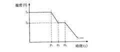
図3は、本発明の好適な実施例によるp型半導体の製造方法を説明するための流れ図であり、図4は、本発明の好適な実施例によるp型半導体の製造方法を説明するためのグラフである。 FIG. 3 is a flowchart for explaining a method of manufacturing a p-type semiconductor according to a preferred embodiment of the present invention, and FIG. 4 is a diagram for explaining a method of manufacturing a p-type semiconductor according to a preferred embodiment of the present invention. It is a graph.
本発明の好適な実施例によると、III族元素の窒化物半導体を製造するために、反応チェンバ内に基板をロードし、基板の温度を、III族元素の窒化物半導体層を成長させるための温度(T1)に上昇させる(S101)。III族元素の窒化物半導体層を成長させるために、基板の温度(T1)は、例えば、1050℃に加熱される。According to a preferred embodiment of the present invention, in order to manufacture a group III element nitride semiconductor, a substrate is loaded into a reaction chamber, and the temperature of the substrate is increased to grow a group III element nitride semiconductor layer. The temperature is increased to T1 (S101). In order to grow the nitride semiconductor layer of the group III element, the temperature (T1 ) of the substrate is heated to 1050 ° C., for example.
基板としては、絶縁性材質のサファイアや炭化ケイ素(SiC)等が用いられるが、伝導性または半導体基板も使用可能である。また、このような異種基板とIII族元素の窒化物半導体層との間の格子不整合を緩和させるために、基板上にバッファ層が形成され、生成したバッファ層上にN型不純物がドープされたIII族元素の窒化物半導体層、すなわち、N型半導体層と活性層が順次形成される。このようなバッファ層は、AlN、InGaN、GaN、またはAlGaN等で形成されてもよい。また、N型半導体層は、不純物のドープ無しでも形成することができるが、Si、Ge、Se、S、またはTe等の不純物をドープして形成することが好ましい。 As the substrate, an insulating material such as sapphire or silicon carbide (SiC) is used, but a conductive or semiconductor substrate can also be used. In addition, in order to alleviate the lattice mismatch between the heterogeneous substrate and the group III element nitride semiconductor layer, a buffer layer is formed on the substrate, and the generated buffer layer is doped with an N-type impurity. A group III element nitride semiconductor layer, that is, an N-type semiconductor layer and an active layer are sequentially formed. Such a buffer layer may be formed of AlN, InGaN, GaN, AlGaN, or the like. In addition, the N-type semiconductor layer can be formed without doping impurities, but is preferably formed by doping impurities such as Si, Ge, Se, S, or Te.
活性層は、単一量子井戸(SQW、Single Quantum Well)または多重量子井戸(MQW、Multi Quantum Well)構造で形成することが好ましい。
次いで、反応チェンバ内に、III族元素のソースガス、p型不純物のソースガス、及びアンモニア等の水素を含有する窒素のソースガスを供給し、p型化合物半導体層を成長させる(S103)。III族元素のソースガスとしては、例えば、トリメチルガリウム(Tri−Methyl Gallium;TMG)、窒素(N)のソースガスは、例えば、アンモニアのような水素を含有するガスが用いられ、キャリアガス(H2またはN2)と一緒に供給される。また、p型不純物のソースガスとしては、Mgを不純物として用いる場合、例えば、Cp2Mgが用いられる。p型不純物としては、Mg以外にも、Be、Sr、Ba、Zn等が使用可能である。一方、ここでは、N型半導体層上に活性層を形成し、活性層上にp型化合物半導体層を成長させるものと記載しているが、その順序は、変更されてもよい。The active layer is preferably formed with a single quantum well (SQW) structure or a multiple quantum well (MQW) structure.
Next, a source gas of a group III element, a source gas of a p-type impurity, and a source gas of nitrogen containing hydrogen such as ammonia are supplied into the reaction chamber to grow a p-type compound semiconductor layer (S103). As a source gas of a group III element, for example, a gas containing hydrogen such as ammonia is used as a source gas of trimethylgallium (TMG) or nitrogen (N), and a carrier gas (H2 or N2 ). In addition, as the source gas of the p-type impurity, for example, Cp2 Mg is used when Mg is used as the impurity. As the p-type impurity, Be, Sr, Ba, Zn, or the like can be used in addition to Mg. On the other hand, although it is described here that an active layer is formed on an N-type semiconductor layer and a p-type compound semiconductor layer is grown on the active layer, the order may be changed.
p型化合物半導体層の成長が完了すると、III族元素のソースガスとp型不純物のソースガスの供給を中断する(S105)。また、p型化合物半導体層が成長された基板を既設定の温度(T2)に冷却させる(S107)。ここで、III族元素のソースガスとp型不純物ソースガスの供給中断ステップは、p型化合物半導体層の冷却ステップの開始後に行われ、または、冷却ステップの開始と同時に行われてもよい。When the growth of the p-type compound semiconductor layer is completed, the supply of the group III element source gas and the p-type impurity source gas is interrupted (S105). Further, the substrate on which the p-type compound semiconductor layer is grown is cooled to a preset temperature (T2 ) (S107). Here, the supply interruption step of the group III element source gas and the p-type impurity source gas may be performed after the start of the cooling step of the p-type compound semiconductor layer, or may be performed simultaneously with the start of the cooling step.
一方、ガス供給中断ステップでは、水素を含有する窒素のソースガスの供給は中断されないので、p型化合物半導体層が冷却される温度(T2)は、本発明では、p型化合物半導体層のp型不純物と水素の結合が行われないような高温に設定され、これにより、p型化合物半導体層の冷却ステップが行われる間、p型不純物と窒素のソースガスに含有された水素の結合が防止されるので、形成されたp型化合物半導体層から水素を除去するための別途のアニール工程を行う必要がなくなる。ここで、p型化合物半導体層の冷却温度(T2)は、例えば、400〜850℃の温度範囲で設定される。400℃以下の温度では、水素とマグネシウムの結合が発生し得るので、400℃以下で、アンモニア等の水素を含有する窒素のソースガスを中断することは好ましくない。On the other hand, in the gas supply interruption step, supply of the nitrogen-containing source gas containing hydrogen is not interrupted. Therefore, in the present invention, the temperature (T2 ) at which the p-type compound semiconductor layer is cooled is set to p of the p-type compound semiconductor layer. This is set to a high temperature that does not cause bonding of the p-type impurity and hydrogen, thereby preventing bonding of hydrogen contained in the p-type impurity and the nitrogen source gas during the cooling step of the p-type compound semiconductor layer. Therefore, it is not necessary to perform a separate annealing step for removing hydrogen from the formed p-type compound semiconductor layer. Here, the cooling temperature (T2 ) of the p-type compound semiconductor layer is set in a temperature range of 400 to 850 ° C., for example. Since a bond between hydrogen and magnesium can occur at a temperature of 400 ° C. or lower, it is not preferable to interrupt the nitrogen source gas containing hydrogen such as ammonia at 400 ° C. or lower.
p型化合物半導体層が成長された基板の温度が、既設定の温度(T2)に冷却されると、水素を含有する窒素ソースガスの供給を中断する(S109)。
また、反応チェンバ内に残留する窒素のソースガスを外部に排出する(S111)。図4を参照すると、窒素ソースガスの排出ステップは、所定の時間間隔(P2からP3)の間行われ、このような時間間隔(P2からP3)の間基板の温度(T2)は、同一に維持される。これは、基板の温度を少なくとも、反応チェンバ内に残存する窒素ソースガスに含有された水素とp型化合物半導体層のp型不純物との間の結合反応を遮断可能な温度以上に維持するためであり、必ずしも同一の温度に維持しなければならないわけではない。When the temperature of the substrate on which the p-type compound semiconductor layer is grown is cooled to a preset temperature (T2 ), the supply of the nitrogen source gas containing hydrogen is interrupted (S109).
Further, the nitrogen source gas remaining in the reaction chamber is discharged to the outside (S111). Referring to FIG. 4, the nitrogen source gas discharge step is performed during a predetermined time interval (P2 to P3 ), and the temperature of the substrate (T2 ) during the time interval (P2 to P3 ). ) Remain the same. This is because the temperature of the substrate is maintained at least above the temperature at which the bonding reaction between hydrogen contained in the nitrogen source gas remaining in the reaction chamber and the p-type impurity of the p-type compound semiconductor layer can be cut off. Yes, it does not necessarily have to be maintained at the same temperature.
水素を含有する窒素ソースガスの供給が中断され、反応チェンバ内に残存する水素を含有する窒素ソースガスが外部に排出されると(P3時点)、基板の温度を反応チェンバ内から引出できる程度まで、例えば、常温に冷却させる(S113)。Is interrupted the supply of the nitrogen source gas containing hydrogen, the nitrogen source gas containing hydrogen remaining in the reaction chamber is discharged to the outside (P3 point), the extent to which the temperature of the substrate can lead from the reaction chamber in the For example, it is cooled to room temperature (S113).
ここで、基板の冷却は、過熱を中断し、そのまま放置し、自然対流方式で行われ、または、反応チェンバを空冷または水冷方式で冷却し、基板の温度を冷却する方式で行われてもよいが、反応チェンバ内に残存するガスを完全に放出させた後、p型不純物と結合していない成分の冷却ガスとして、例えば、窒素(N2)または不活性ガスであるアルゴン(Ar)ガスを注入し、基板を冷却させることがより好ましい。Here, the cooling of the substrate may be performed by interrupting overheating and leaving the substrate as it is, by a natural convection method, or by a method of cooling the temperature of the substrate by cooling the reaction chamber by air cooling or water cooling. However, after the gas remaining in the reaction chamber is completely released, for example, nitrogen (N2 ) or an inert gas such as argon (Ar) gas is used as a cooling gas for components not bonded to the p-type impurities. More preferably, it is injected and the substrate is cooled.
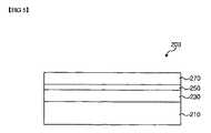
図5は、本発明の好適な実施例により製造されたp型化合物半導体を備える(Al、Ga、In)N系化合物半導体の概略的な縦断面図である。
本実施例による(Al、Ga、In)N系化合物半導体200では、基板210上にN層230、活性層250、及びp層270が形成されている。基板210は、導電性または半導電性の金属、Si、SiC、またはGaN等で形成されてもよく、それ自体でN型電極としての機能を行うことができる。また、基板210は、サファイアまたはスピネルで形成されてもよい。N層230と基板210との間には、上述したようにバッファ層(図示せず)を形成してもよい。FIG. 5 is a schematic longitudinal sectional view of an (Al, Ga, In) N-based compound semiconductor including a p-type compound semiconductor manufactured according to a preferred embodiment of the present invention.
In the (Al, Ga, In) N-based
本実施例において、p型化合物半導体層であるp層270は、図3を参照して上述したように、アニール工程無しで形成される。このため、反応チェンバ内でp層270の成長が完了すると、III族元素のソースガスとp型不純物のソースガスの供給を中断し、p型化合物半導体層が成長された基板を既設定の温度(T2)に冷却させた後、窒素ソースガスの供給を中断する。ここで、p型化合物半導体層の冷却温度(T2)は、例えば、400〜850℃の温度範囲で設定される。次いで、反応チェンバ内に残存する窒素ソースガスが外部に放出されると、基板の温度を、反応チェンバ内から引出できる程度に窒素(N2)または不活性気体であるアルゴン(Ar)ガスを用いて冷却させ、p型化合物半導体層270が形成される。このように形成されたp型化合物半導体層は、水素と結合されていないp型不純物を含み、これにより、水素を除去するための別途のアニール工程を行う必要がない。In this embodiment, the
一方、図5には、基板210がN層230に隣接して配置された実施例について説明しているが、本発明は、これに限られず、基板がp層に隣接して配置された構成にも適用可能である。このような構成でも、上述及び図示した実施例と同様に同一の機能及び効果が提供される。 On the other hand, FIG. 5 illustrates an embodiment in which the
また、本発明と関連して、上述されている(Al、Ga、In)N系化合物半導体は、AlxInyGa1−x−yN(0≦x、y、x+y≦1)を含むことはもとより、このような化合物半導体は、例えば、発光素子(LED、Light Emitting Diode)、レーザ素子(LD、Laser Diode)、ヘテロ接合バイポーラトランジスタ、電界効果トランジスタ、または光検知器以外にも様々な分野に適用可能である。Further, in connection with the present invention are described above (Al, Ga, In) N-based compound semiconductorcomprisesAl x In y Ga 1-x -y N (0 ≦ x, y, x + y ≦ 1) and Of course, such compound semiconductors are not limited to light emitting elements (LEDs, light emitting diodes), laser elements (LDs, laser diodes), heterojunction bipolar transistors, field effect transistors, or photodetectors. Applicable to the field.
図6及び図7は、本発明の好適な実施例によるp型化合物半導体層の形成方法による効果を説明するための図であり、原子間力顕微鏡(Atomic Force Microscope:AFM)のイメージを示す。 6 and 7 are diagrams for explaining the effect of the method for forming a p-type compound semiconductor layer according to a preferred embodiment of the present invention, and show an image of an atomic force microscope (AFM).
p型半導体層を形成した後、アンモニアガス供給を直ちに中断すると、急激な冷却により、Gaが蒸発し、これにより、p型半導体層の表面が損傷される。図6aは、このようなGa蒸発による発光ダイオードウエハの表面の損傷を示す。 If the supply of ammonia gas is immediately interrupted after forming the p-type semiconductor layer, Ga is evaporated by rapid cooling, thereby damaging the surface of the p-type semiconductor layer. FIG. 6a shows the damage of the surface of the light emitting diode wafer due to such Ga evaporation.
しかしながら、本発明の好適な実施例によるp型半導体層の形成方法によると、p型半導体層を形成し、基板を既設定の温度(T2)に冷却させた後、水素を含有する窒素ソースガスの供給を中断し、所定の時間間隔の間、前記温度(T2)を維持するので、基板の急激な冷却が防止され、結晶体の損傷を防止することができる。However, according to the method of forming a p-type semiconductor layer according to a preferred embodiment of the present invention, after forming the p-type semiconductor layer and cooling the substrate to a preset temperature (T2 ), a nitrogen source containing hydrogen Since the supply of gas is interrupted and the temperature (T2 ) is maintained for a predetermined time interval, rapid cooling of the substrate can be prevented and damage to the crystal can be prevented.
図7は、本発明によるp型半導体層の形成方法により形成された発光ダイオードウエハの表面を撮像した原子間力顕微鏡のイメージであり、図6のウエハの表面とは異なり、ウエハの表面の損傷がないことが分かる。 FIG. 7 is an image of an atomic force microscope that images the surface of a light emitting diode wafer formed by the method for forming a p-type semiconductor layer according to the present invention. Unlike the wafer surface of FIG. You can see that there is no.
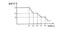
図8は、本発明の他の好適な実施例によるp型半導体の製造方法を説明するための流れ図であり、図9及び図10は、本発明の他の好適な実施例によるp型半導体の製造方法を説明するためのグラフである。 FIG. 8 is a flowchart for explaining a method of manufacturing a p-type semiconductor according to another preferred embodiment of the present invention, and FIGS. 9 and 10 illustrate a p-type semiconductor according to another preferred embodiment of the present invention. It is a graph for demonstrating a manufacturing method.
本発明の好適な実施例によると、図8の一部のステップ(S301、S303、S305、S307)は、図3のステップ(S101、S103、S105、S107)と事実上類似するので、その説明を省略する。 According to a preferred embodiment of the present invention, some steps (S301, S303, S305, S307) in FIG. 8 are substantially similar to steps (S101, S103, S105, S107) in FIG. Is omitted.
基板が既設定の温度(T2)に冷却されると、III族元素のソースガスとn型またはp型不純物のソースガス及び水素を含有する窒素のソースガスを供給し、ITOトンネル層を成長させる(S309)。ITOトンネル層は、p型化合物半導体層と、その上に形成されるITOトンネル層のオーム接触のために形成され、ITO透明電極層とp型化合物半導体層との間の電気抵抗、及びこれによる意図しない界面発熱を減らすことができる。ITOトンネル層は、(Al、Ga、In)N系半導体層であり、n型またはp型不純物を高濃度にドープして形成されてもよい。When the substrate is cooled to a preset temperature (T2 ), a group III element source gas, an n-type or p-type impurity source gas, and a nitrogen-containing source gas containing hydrogen are supplied to grow an ITO tunnel layer. (S309). The ITO tunnel layer is formed for ohmic contact between the p-type compound semiconductor layer and the ITO tunnel layer formed thereon, and the electric resistance between the ITO transparent electrode layer and the p-type compound semiconductor layer, and thereby Unintentional interfacial heat generation can be reduced. The ITO tunnel layer is an (Al, Ga, In) N-based semiconductor layer, and may be formed by doping an n-type or p-type impurity at a high concentration.
一方、ITOトンネル層の成長温度は、400〜900℃の温度範囲であるので、前記p型化合物半導体層の冷却温度(T2)は、このような範囲内で設定されてもよい。ITOトンネル層の成長が完成すると、III族元素のソースガスとn型またはp型不純物のソースガスの供給は中断する。On the other hand, since the growth temperature of the ITO tunnel layer is in the temperature range of 400 to 900 ° C., the cooling temperature (T2 ) of the p-type compound semiconductor layer may be set within such a range. When the growth of the ITO tunnel layer is completed, the supply of the group III element source gas and the source gas of the n-type or p-type impurity is interrupted.
次いで、基板を既設定の温度(T3)に冷却させ(S311)、水素を含有する窒素のソースガスの供給を中断し(S313)、反応チェンバ内に残留する水素を含有した窒素のソースガスを外部に排出させる(S314)。p型化合物半導体層が冷却され、水素を含有する窒素のソースガスの供給が中断される温度(T3)は、本発明では、p型化合物半導体層のp型不純物と水素の結合が行われないような高温に設定され、これにより、p型化合物半導体層の冷却ステップが行われる間、p型不純物と窒素のソースガスに含有された水素の結合が防止されるので、形成されたp型化合物半導体層から水素を除去するための別途のアニール工程を行う必要がなくなる。Next, the substrate is cooled to a preset temperature (T3 ) (S 311), the supply of the nitrogen source gas containing hydrogen is interrupted (S 313), and the nitrogen source gas containing hydrogen remaining in the reaction chamber is interrupted. Is discharged to the outside (S314). The temperature at which the p-type compound semiconductor layer is cooled and the supply of the nitrogen-containing source gas containing hydrogen is interrupted (T3 ) in the present invention, in which the p-type impurity of the p-type compound semiconductor layer is combined with hydrogen. The p-type compound semiconductor layer is formed at a high temperature so that bonding between hydrogen contained in the p-type impurity and the nitrogen source gas is prevented during the cooling step of the p-type compound semiconductor layer. There is no need to perform a separate annealing step for removing hydrogen from the compound semiconductor layer.
ここで、p型化合物半導体層を冷却させ、水素を含有した窒素のソースガスの供給を中断する温度(T3)は、例えば、400〜850℃の温度範囲で設定される。400℃以下の温度では、水素とマグネシウムの結合が発生し得るので、400℃以下で、アンモニア等の水素を含有する窒素のソースガスを中断することは好ましくない。Here, the temperature (T3 ) at which the p-type compound semiconductor layer is cooled and the supply of the nitrogen-containing source gas containing hydrogen is stopped is set in a temperature range of 400 to 850 ° C., for example. Since a bond between hydrogen and magnesium can occur at a temperature of 400 ° C. or lower, it is not preferable to interrupt the nitrogen source gas containing hydrogen such as ammonia at 400 ° C. or lower.
一方、前記ITOトンネル層の成長温度(T2)を、水素を含有した窒素のソースガスの供給中断ステップ遂行温度(T3)と一致させ、ITOトンネル層の成長が完了すると、水素を含有した窒素のソースガスの供給を中断し、ガスが反応チェンバから排出されるまで、前記温度(T2)を維持した後、基板を冷却してもよい。Meanwhile, the growth temperature (T2 ) of the ITO tunnel layer is made to coincide with the supply interruption step execution temperature (T3 ) of the nitrogen source gas containing hydrogen, and when the growth of the ITO tunnel layer is completed, hydrogen is contained. The substrate may be cooled after interrupting the supply of nitrogen source gas and maintaining the temperature (T2 ) until the gas is exhausted from the reaction chamber.
図9を参照すると、ITOトンネル層は、既設定の温度(T2)で行われ、以降、基板が既設定の温度(T3)に冷却されると、水素を含有する窒素のソースガスの排出ステップが、所定の時間間隔(P4からP5)の間行われ、このような時間間隔(P4からP5)の間、基板の温度(T3)は同一に維持される。これは、基板の温度を少なくとも、反応チェンバ内に残存する水素を含有する窒素ソースガスに含有された水素とp型化合物半導体層のp型不純物との間の結合反応を遮断可能な温度以上に維持するためであり、必ずしも同一の温度に維持しなければならないわけではない。Referring to FIG. 9, the ITO tunnel layer is performed at a preset temperature (T2 ), and thereafter, when the substrate is cooled to the preset temperature (T3 ), the source gas of nitrogen containing hydrogen is reduced. discharge step is carried out between (from P4 P5) a predetermined time interval, between (from P4 P5) such time interval, the temperature of the substrate (T3) is maintained at the same. This is because the temperature of the substrate is at least higher than the temperature at which the bonding reaction between hydrogen contained in the nitrogen source gas containing hydrogen remaining in the reaction chamber and the p-type impurity of the p-type compound semiconductor layer can be cut off. This is for the purpose of maintaining, and it is not always necessary to maintain the same temperature.
一方、図10は、ITOトンネル層の成長温度(T2)と、水素が含有された窒素のソースガスの供給中断温度(T3)を一致させた場合の例であり、ITOトンネル層の成長が一定の時間(P2からP6)の間行われた後、水素を含有する窒素のソースガスの供給を中断し、残留ガスが反応チェンバから排出されるまで、一定の時間(P6からP7)の間、同一の温度(T2)が維持される。On the other hand, FIG. 10 shows an example in which the growth temperature (T2 ) of the ITO tunnel layer and the supply interruption temperature (T3 ) of the nitrogen source gas containing hydrogen coincide with each other. Is performed for a certain period of time (P2 to P6 ), then the supply of nitrogen-containing source gas containing hydrogen is interrupted and the remaining gas is discharged from the reaction chamber for a certain period of time (from P6 The same temperature (T2 ) is maintained during P7 ).
水素を含有する窒素ソースガスの供給が中断され、反応チェンバ内に残存する水素を含有する窒素ソースガスが外部に排出されると(図9のP5時点または図10のP7時点)、基板の温度を反応チェンバ内から引出できる程度まで、例えば、常温に冷却させる(S315)。この場合、窒素ガスを冷却ガスとして用いてもよい。Is interrupted the supply of the nitrogen source gas containing hydrogen, the nitrogen source gas containing hydrogen remaining in the reaction chamber is discharged to the outside (P7 time points P5 times or 10 in FIG. 9), the substrate Is cooled to room temperature, for example, to such an extent that it can be drawn out from the reaction chamber (S315). In this case, nitrogen gas may be used as the cooling gas.
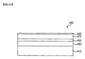
図11は、本発明の他の好適な実施例により製造されたp型半導体を備える(Al、Ga、In)N系化合物半導体の概略的な縦断面図である。
本実施例による(Al、Ga、In)N系化合物半導体400では、基板410上に、N層430、活性層450、p層470、及びITOトンネル層490が形成されている。基板410は、導電性または半導電性の金属、Si、SiC、またはGaN等で形成されてもよく、それ自体でN型電極としての機能を行うことができる。また、基板410は、サファイアまたはスピネルで形成されてもよい。N層430と基板410との間には、上述したようにバッファ層(図示せず)を形成してもよい。FIG. 11 is a schematic longitudinal sectional view of an (Al, Ga, In) N-based compound semiconductor including a p-type semiconductor manufactured according to another preferred embodiment of the present invention.
In the (Al, Ga, In) N-based
本実施例において、p型化合物半導体層であるp層470は、図8を参照して上述したように、アニール工程無しで形成される。このため、反応チェンバ内でp層470の成長が完了すると、III族元素のソースガスとp型不純物のソースガスの供給を中断し、p型化合物半導体層が成長された基板を既設定の温度(T2)に冷却させ、ITOトンネル層490を成長させた後、上述したように、同一の温度(T2)で、または既設定の温度(T3)に冷却した後、水素を含有した窒素ソースガスの供給を中断する。ここで、ITOトンネル層490の成長温度(T2)は、例えば、400〜900℃の温度範囲で設定され、水素を含有した窒素のソースガス供給中断温度(T3)は、400〜850℃で設定される。したがって、二つの温度を一致させ、ITOトンネル層490の成長が完了すると、水素を含有した窒素のソースガスの供給を中断し、一定の時間の間温度を維持した後、基板を冷却してもよい。次いで、反応チェンバ内に残存する水素を含有する窒素ソースガスが外部に放出されると、基板の温度を、反応チェンバ内から引出できる程度に冷却させる。このように形成されたp型化合物半導体層は、水素と結合されていないp型不純物を含み、これにより、水素を除去するための別途のアニール工程を行う必要がない。In this embodiment, the
一方、図11には、基板410がN層430に隣接して配置された実施例について説明しているが、本発明は、これに限られず、基板がp層に隣接して配置された構成にも適用可能である。このような構成でも、上述及び図示した実施例と同様に同一の機能及び効果が提供される。 On the other hand, FIG. 11 illustrates an embodiment in which the
また、本発明と関連して、上述されている(Al、Ga、In)N系化合物半導体は、AlxInyGa1−x−yN(0≦x、y、x+y≦1)を含むことはもとより、このような化合物半導体は、例えば、発光素子(LED、Light Emitting Diode)、レーザ素子(LD、Laser Diode)、ヘテロ接合バイポーラトランジスタ、電界効果トランジスタ、または光検知器以外にも様々な分野に適用可能である。Further, in connection with the present invention are described above (Al, Ga, In) N-based compound semiconductorcomprisesAl x In y Ga 1-x -y N (0 ≦ x, y, x + y ≦ 1) and Of course, such compound semiconductors are not limited to light emitting elements (LEDs, light emitting diodes), laser elements (LDs, laser diodes), heterojunction bipolar transistors, field effect transistors, or photodetectors. Applicable to the field.
Claims (13)
Translated fromJapanese前記反応チェンバ内に、III族元素のソースガス、p型不純物のソースガス、及び水素を含有する窒素のソースガスを供給し、p型化合物半導体層を成長させるステップと、
前記p型化合物半導体層の成長が完了した後、前記III族元素のソースガス及び前記p型不純物のソースガスの供給を中断し、前記基板の温度を第2の温度に冷却させるステップと、
前記第2の温度で、前記水素を含有する窒素のソースガスの供給を中断するステップと、
アルゴンガスを供給し、前記基板の温度を常温に冷却させるステップと、
を含むことを特徴とするp型化合物半導体層の形成方法。Raising the substrate loaded in the reaction chamber to a first temperature;
Supplying a group III element source gas, a p-type impurity source gas, and a nitrogen-containing nitrogen source gas into the reaction chamber to grow a p-type compound semiconductor layer;
After the growth of the p-type compound semiconductor layer is completed, the supply of the group III element source gas and the p-type impurity source gas is interrupted, and the temperature of the substrate is cooled to a second temperature;
Interrupting the supply of the nitrogen-containing source gas containing hydrogen at the second temperature;
Supplying argon gas and cooling the temperature of the substrate to room temperature;
A method for forming a p-type compound semiconductor layer, comprising:
前記反応チェンバ内に、III族元素のソースガス、p型不純物のソースガス、及び水素を含有する窒素のソースガスを供給し、p型化合物半導体層を成長させるステップと、
前記p型化合物半導体層の成長が完了した後、前記III族元素のソースガス及び前記p型不純物のソースガスの供給を中断し、前記基板の温度を第2の温度に冷却させるステップと、
前記第2の温度で、前記III族元素のソースガス、n型またはp型不純物のソースガス、及び前記水素を含有する窒素のソースガスを供給し、ITOトンネル層を成長させるステップと、
前記ITOトンネル層の成長が完了した後、前記III族元素のソースガス、前記n型またはp型不純物のソースガスの供給を中断するステップと、
前記基板の温度を第3の温度に冷却させ、前記水素を含有する窒素のソースガスを中断するステップと、
前記基板の温度を常温に冷却させるステップと、
を含むことを特徴とするp型化合物半導体層の形成方法。Raising the substrate loaded in the reaction chamber to a first temperature;
Supplying a group III element source gas, a p-type impurity source gas, and a nitrogen-containing nitrogen source gas into the reaction chamber to grow a p-type compound semiconductor layer;
After the growth of the p-type compound semiconductor layer is completed, the supply of the group III element source gas and the p-type impurity source gas is interrupted, and the temperature of the substrate is cooled to a second temperature;
Supplying a source gas of the group III element, a source gas of an n-type or p-type impurity, and a source gas of nitrogen containing hydrogen at the second temperature, and growing an ITO tunnel layer;
Interrupting the supply of the group III element source gas, the n-type or p-type impurity source gas after the growth of the ITO tunnel layer is completed;
Cooling the temperature of the substrate to a third temperature and interrupting the source gas of nitrogen containing hydrogen;
Cooling the temperature of the substrate to room temperature;
A method for forming a p-type compound semiconductor layer, comprising:
Applications Claiming Priority (3)
| Application Number | Priority Date | Filing Date | Title |
|---|---|---|---|
| KR1020060060820AKR100707798B1 (en) | 2006-06-30 | 2006-06-30 | P-type compound semiconductor layer formation method |
| KR1020060060822AKR100757801B1 (en) | 2006-06-30 | 2006-06-30 | P-type compound semiconductor layer formation method |
| PCT/KR2007/003185WO2008002104A1 (en) | 2006-06-30 | 2007-06-29 | Method of forming p-type compound semiconductor layer |
Related Child Applications (1)
| Application Number | Title | Priority Date | Filing Date |
|---|---|---|---|
| JP2012223419ADivisionJP5947183B2 (en) | 2006-06-30 | 2012-10-05 | Method for forming p-type compound semiconductor layer |
Publications (1)
| Publication Number | Publication Date |
|---|---|
| JP2009543331Atrue JP2009543331A (en) | 2009-12-03 |
Family
ID=38845810
Family Applications (2)
| Application Number | Title | Priority Date | Filing Date |
|---|---|---|---|
| JP2009517985AWithdrawnJP2009543331A (en) | 2006-06-30 | 2007-06-29 | Method for forming p-type compound semiconductor layer |
| JP2012223419AExpired - Fee RelatedJP5947183B2 (en) | 2006-06-30 | 2012-10-05 | Method for forming p-type compound semiconductor layer |
Family Applications After (1)
| Application Number | Title | Priority Date | Filing Date |
|---|---|---|---|
| JP2012223419AExpired - Fee RelatedJP5947183B2 (en) | 2006-06-30 | 2012-10-05 | Method for forming p-type compound semiconductor layer |
Country Status (4)
| Country | Link |
|---|---|
| US (2) | US7682953B2 (en) |
| JP (2) | JP2009543331A (en) |
| DE (1) | DE112007000059T5 (en) |
| WO (1) | WO2008002104A1 (en) |
Cited By (1)
| Publication number | Priority date | Publication date | Assignee | Title |
|---|---|---|---|---|
| JP2013016863A (en)* | 2006-06-30 | 2013-01-24 | Seoul Opto Devices Co Ltd | P-type compound semiconductor layer formation method |
Families Citing this family (4)
| Publication number | Priority date | Publication date | Assignee | Title |
|---|---|---|---|---|
| JP3110002B2 (en) | 1997-06-30 | 2000-11-20 | 株式会社巴技術研究所 | Butterfly valve |
| US8946674B2 (en) | 2005-08-31 | 2015-02-03 | University Of Florida Research Foundation, Inc. | Group III-nitrides on Si substrates using a nanostructured interlayer |
| US20200135489A1 (en)* | 2018-10-31 | 2020-04-30 | Atomera Incorporated | Method for making a semiconductor device including a superlattice having nitrogen diffused therein |
| CN117051385A (en)* | 2023-07-03 | 2023-11-14 | 华灿光电(苏州)有限公司 | Cavity cleaning method of MOCVD equipment |
Citations (3)
| Publication number | Priority date | Publication date | Assignee | Title |
|---|---|---|---|---|
| JPH06326416A (en)* | 1993-03-15 | 1994-11-25 | Toshiba Corp | Compound semiconductor element |
| JPH09199758A (en)* | 1996-01-19 | 1997-07-31 | Nec Corp | Low resistance p-type gallium nitride compound semiconductor vapor phase growth method |
| JP2003133649A (en)* | 2001-10-29 | 2003-05-09 | Sharp Corp | Nitride semiconductor laser device, method of manufacturing nitride semiconductor laser device, and semiconductor optical device provided with the same |
Family Cites Families (11)
| Publication number | Priority date | Publication date | Assignee | Title |
|---|---|---|---|---|
| US5306662A (en) | 1991-11-08 | 1994-04-26 | Nichia Chemical Industries, Ltd. | Method of manufacturing P-type compound semiconductor |
| JP3620105B2 (en)* | 1995-07-27 | 2005-02-16 | 日立電線株式会社 | Method for producing gallium nitride crystal |
| US20020017650A1 (en)* | 1997-11-18 | 2002-02-14 | Technologies & Devices | III-V compound semiconductor device with an InGaN1-x-yPxASy non-continuous quantum dot layer |
| US6476420B2 (en)* | 1997-11-18 | 2002-11-05 | Technologies And Devices International, Inc. | P-N homojunction-based structures utilizing HVPE growth III-V compound layers |
| JP3522610B2 (en)* | 1999-10-15 | 2004-04-26 | 松下電器産業株式会社 | Method for manufacturing p-type nitride semiconductor |
| JP2004134750A (en)* | 2002-09-19 | 2004-04-30 | Toyoda Gosei Co Ltd | Method for producing p-type group III nitride compound semiconductor |
| KR20050025054A (en)* | 2003-09-03 | 2005-03-11 | 삼성전기주식회사 | AlGaInN based P-N Diode and Fabrication Method thereof |
| TWI229952B (en)* | 2004-05-07 | 2005-03-21 | United Epitaxy Co Ltd | Semiconductor light emitting device and method of making the same |
| US20080135868A1 (en)* | 2004-10-01 | 2008-06-12 | Mitsubishi Cable Industries, Ltd. | Nitride Semiconductor Light Emitting Element and Method for Manufacturing the Same |
| JP4720519B2 (en)* | 2006-01-23 | 2011-07-13 | パナソニック株式会社 | Method for manufacturing p-type nitride semiconductor |
| JP2009543331A (en)* | 2006-06-30 | 2009-12-03 | ソウル オプト デバイス カンパニー リミテッド | Method for forming p-type compound semiconductor layer |
- 2007
- 2007-06-29JPJP2009517985Apatent/JP2009543331A/ennot_activeWithdrawn
- 2007-06-29USUS12/090,305patent/US7682953B2/enactiveActive
- 2007-06-29WOPCT/KR2007/003185patent/WO2008002104A1/enactiveApplication Filing
- 2007-06-29DEDE112007000059Tpatent/DE112007000059T5/ennot_activeCeased
- 2009
- 2009-09-16USUS12/560,891patent/US8470697B2/ennot_activeExpired - Fee Related
- 2012
- 2012-10-05JPJP2012223419Apatent/JP5947183B2/ennot_activeExpired - Fee Related
Patent Citations (3)
| Publication number | Priority date | Publication date | Assignee | Title |
|---|---|---|---|---|
| JPH06326416A (en)* | 1993-03-15 | 1994-11-25 | Toshiba Corp | Compound semiconductor element |
| JPH09199758A (en)* | 1996-01-19 | 1997-07-31 | Nec Corp | Low resistance p-type gallium nitride compound semiconductor vapor phase growth method |
| JP2003133649A (en)* | 2001-10-29 | 2003-05-09 | Sharp Corp | Nitride semiconductor laser device, method of manufacturing nitride semiconductor laser device, and semiconductor optical device provided with the same |
Cited By (1)
| Publication number | Priority date | Publication date | Assignee | Title |
|---|---|---|---|---|
| JP2013016863A (en)* | 2006-06-30 | 2013-01-24 | Seoul Opto Devices Co Ltd | P-type compound semiconductor layer formation method |
Also Published As
| Publication number | Publication date |
|---|---|
| DE112007000059T5 (en) | 2008-08-21 |
| US20090163002A1 (en) | 2009-06-25 |
| WO2008002104A1 (en) | 2008-01-03 |
| US8470697B2 (en) | 2013-06-25 |
| JP2013016863A (en) | 2013-01-24 |
| US20100003810A1 (en) | 2010-01-07 |
| JP5947183B2 (en) | 2016-07-06 |
| US7682953B2 (en) | 2010-03-23 |
Similar Documents
| Publication | Publication Date | Title |
|---|---|---|
| JP2872096B2 (en) | Vapor phase growth method of low resistance p-type gallium nitride based compound semiconductor | |
| US20110177678A1 (en) | Method for manufacturing nitride semiconductor device | |
| WO2007083647A1 (en) | Nitride semiconductor light-emitting device | |
| JP5947183B2 (en) | Method for forming p-type compound semiconductor layer | |
| JP3243111B2 (en) | Compound semiconductor device | |
| JP3603598B2 (en) | Method for manufacturing group 3-5 compound semiconductor | |
| JP5568009B2 (en) | Semiconductor light emitting device and manufacturing method thereof | |
| JP2004134750A (en) | Method for producing p-type group III nitride compound semiconductor | |
| JP4940670B2 (en) | Method for fabricating nitride semiconductor light emitting device | |
| JP3741528B2 (en) | Method for manufacturing gallium nitride based semiconductor device | |
| JP3322179B2 (en) | Gallium nitride based semiconductor light emitting device | |
| CN101868848B (en) | Method for fabricating p-type gallium nitride-based semiconductor, method for fabricating nitride-based semiconductor element, and method for fabricating epitaxial wafer | |
| JP3497790B2 (en) | Method for manufacturing p-type gallium nitride based semiconductor and light emitting device using p-type gallium nitride based semiconductor | |
| JP2004087565A (en) | Method for manufacturing gallium nitride-based semiconductor light emitting device | |
| JP3785059B2 (en) | Manufacturing method of nitride semiconductor | |
| KR100707798B1 (en) | P-type compound semiconductor layer formation method | |
| KR100757801B1 (en) | P-type compound semiconductor layer formation method | |
| KR100737820B1 (en) | P-type compound semiconductor layer formation method | |
| JP4137223B2 (en) | Method for producing compound semiconductor | |
| JP2007027248A (en) | Method for producing p-type group III nitride semiconductor layer and light emitting device | |
| JP2003264345A (en) | Nitride semiconductor light emitting device | |
| WO2010116424A1 (en) | Semiconductor device manufacturing method | |
| JP2000311865A (en) | Compound semiconductor device and method of manufacturing the same | |
| JP3505167B2 (en) | Method of manufacturing gallium nitride based compound semiconductor light emitting device | |
| JP3557875B2 (en) | GaN-based semiconductor device and method of manufacturing the same |
Legal Events
| Date | Code | Title | Description |
|---|---|---|---|
| RD03 | Notification of appointment of power of attorney | Free format text:JAPANESE INTERMEDIATE CODE: A7423 Effective date:20091020 | |
| RD04 | Notification of resignation of power of attorney | Free format text:JAPANESE INTERMEDIATE CODE: A7424 Effective date:20091021 | |
| A621 | Written request for application examination | Free format text:JAPANESE INTERMEDIATE CODE: A621 Effective date:20100310 | |
| A977 | Report on retrieval | Free format text:JAPANESE INTERMEDIATE CODE: A971007 Effective date:20120113 | |
| A131 | Notification of reasons for refusal | Free format text:JAPANESE INTERMEDIATE CODE: A131 Effective date:20120117 | |
| A521 | Request for written amendment filed | Free format text:JAPANESE INTERMEDIATE CODE: A523 Effective date:20120417 | |
| A02 | Decision of refusal | Free format text:JAPANESE INTERMEDIATE CODE: A02 Effective date:20120605 | |
| A521 | Request for written amendment filed | Free format text:JAPANESE INTERMEDIATE CODE: A523 Effective date:20121005 | |
| A911 | Transfer to examiner for re-examination before appeal (zenchi) | Free format text:JAPANESE INTERMEDIATE CODE: A911 Effective date:20121016 | |
| A912 | Re-examination (zenchi) completed and case transferred to appeal board | Free format text:JAPANESE INTERMEDIATE CODE: A912 Effective date:20121122 | |
| A761 | Written withdrawal of application | Free format text:JAPANESE INTERMEDIATE CODE: A761 Effective date:20130618 |