JP2009529220A - Light emitting diode projection system - Google Patents
Light emitting diode projection systemDownload PDFInfo
- Publication number
- JP2009529220A JP2009529220AJP2008558263AJP2008558263AJP2009529220AJP 2009529220 AJP2009529220 AJP 2009529220AJP 2008558263 AJP2008558263 AJP 2008558263AJP 2008558263 AJP2008558263 AJP 2008558263AJP 2009529220 AJP2009529220 AJP 2009529220A
- Authority
- JP
- Japan
- Prior art keywords
- led
- light source
- imaging optical
- optical element
- entrance
- Prior art date
- Legal status (The legal status is an assumption and is not a legal conclusion. Google has not performed a legal analysis and makes no representation as to the accuracy of the status listed.)
- Pending
Links
- 238000003384imaging methodMethods0.000claimsabstractdescription43
- 238000005286illuminationMethods0.000claimsabstractdescription25
- 230000003287optical effectEffects0.000claimsdescription56
- 239000007787solidSubstances0.000claimsdescription24
- 239000000463materialSubstances0.000claimsdescription15
- 230000003595spectral effectEffects0.000claimsdescription12
- 238000000034methodMethods0.000claimsdescription11
- 239000003086colorantSubstances0.000claimsdescription7
- 239000008393encapsulating agentSubstances0.000claimsdescription7
- 238000005538encapsulationMethods0.000claimsdescription7
- 238000010521absorption reactionMethods0.000claimsdescription6
- 239000003989dielectric materialSubstances0.000claimsdescription6
- 230000000694effectsEffects0.000claimsdescription5
- 230000005855radiationEffects0.000claimsdescription5
- 239000007788liquidSubstances0.000claims1
- 239000000203mixtureSubstances0.000claims1
- 230000007246mechanismEffects0.000abstractdescription3
- 238000010586diagramMethods0.000description37
- 238000013461designMethods0.000description23
- 230000008901benefitEffects0.000description22
- 230000004907fluxEffects0.000description22
- 239000000758substrateSubstances0.000description16
- 238000009826distributionMethods0.000description12
- 230000006870functionEffects0.000description11
- 238000013459approachMethods0.000description9
- 238000000576coating methodMethods0.000description9
- 150000001875compoundsChemical class0.000description9
- 239000011248coating agentSubstances0.000description8
- 230000008878couplingEffects0.000description7
- 238000010168coupling processMethods0.000description7
- 238000005859coupling reactionMethods0.000description7
- 238000012053enzymatic serum creatinine assayMethods0.000description7
- 239000011521glassSubstances0.000description6
- 238000000605extractionMethods0.000description5
- 230000006872improvementEffects0.000description5
- QSHDDOUJBYECFT-UHFFFAOYSA-NmercuryChemical compound[Hg]QSHDDOUJBYECFT-UHFFFAOYSA-N0.000description5
- 229910052753mercuryInorganic materials0.000description5
- 229910052724xenonInorganic materials0.000description5
- FHNFHKCVQCLJFQ-UHFFFAOYSA-Nxenon atomChemical compound[Xe]FHNFHKCVQCLJFQ-UHFFFAOYSA-N0.000description5
- 239000002131composite materialSubstances0.000description4
- 238000001816coolingMethods0.000description4
- 230000007423decreaseEffects0.000description4
- 229910052751metalInorganic materials0.000description4
- 239000002184metalSubstances0.000description4
- 238000001228spectrumMethods0.000description4
- 238000003491arrayMethods0.000description3
- 230000005540biological transmissionEffects0.000description3
- 230000008859changeEffects0.000description3
- 239000004973liquid crystal related substanceSubstances0.000description3
- 238000002156mixingMethods0.000description3
- 239000004033plasticSubstances0.000description3
- 230000004044responseEffects0.000description3
- XUIMIQQOPSSXEZ-UHFFFAOYSA-NSiliconChemical compound[Si]XUIMIQQOPSSXEZ-UHFFFAOYSA-N0.000description2
- 230000001419dependent effectEffects0.000description2
- 230000017525heat dissipationEffects0.000description2
- 238000000265homogenisationMethods0.000description2
- 229910001507metal halideInorganic materials0.000description2
- 150000005309metal halidesChemical class0.000description2
- 238000012986modificationMethods0.000description2
- 230000004048modificationEffects0.000description2
- 230000010287polarizationEffects0.000description2
- 229910052710siliconInorganic materials0.000description2
- 239000010703siliconSubstances0.000description2
- OKTJSMMVPCPJKN-UHFFFAOYSA-NCarbonChemical compound[C]OKTJSMMVPCPJKN-UHFFFAOYSA-N0.000description1
- RYGMFSIKBFXOCR-UHFFFAOYSA-NCopperChemical compound[Cu]RYGMFSIKBFXOCR-UHFFFAOYSA-N0.000description1
- OAICVXFJPJFONN-UHFFFAOYSA-NPhosphorusChemical compound[P]OAICVXFJPJFONN-UHFFFAOYSA-N0.000description1
- NIXOWILDQLNWCW-UHFFFAOYSA-Nacrylic acid groupChemical groupC(C=C)(=O)ONIXOWILDQLNWCW-UHFFFAOYSA-N0.000description1
- 230000004075alterationEffects0.000description1
- 229910052782aluminiumInorganic materials0.000description1
- XAGFODPZIPBFFR-UHFFFAOYSA-NaluminiumChemical compound[Al]XAGFODPZIPBFFR-UHFFFAOYSA-N0.000description1
- 238000005219brazingMethods0.000description1
- 238000004364calculation methodMethods0.000description1
- 238000007796conventional methodMethods0.000description1
- 229910052802copperInorganic materials0.000description1
- 239000010949copperSubstances0.000description1
- 238000012937correctionMethods0.000description1
- 238000004042decolorizationMethods0.000description1
- 238000011161developmentMethods0.000description1
- 230000018109developmental processEffects0.000description1
- 229910003460diamondInorganic materials0.000description1
- 239000010432diamondSubstances0.000description1
- 230000005672electromagnetic fieldEffects0.000description1
- 238000005516engineering processMethods0.000description1
- 238000005530etchingMethods0.000description1
- 230000005284excitationEffects0.000description1
- 229910002804graphiteInorganic materials0.000description1
- 239000010439graphiteSubstances0.000description1
- 239000004519greaseSubstances0.000description1
- 210000003128headAnatomy0.000description1
- 230000020169heat generationEffects0.000description1
- 238000009413insulationMethods0.000description1
- 238000000608laser ablationMethods0.000description1
- 238000003754machiningMethods0.000description1
- 238000012423maintenanceMethods0.000description1
- 238000004519manufacturing processMethods0.000description1
- 238000005259measurementMethods0.000description1
- 238000012544monitoring processMethods0.000description1
- 238000004806packaging method and processMethods0.000description1
- 230000002688persistenceEffects0.000description1
- 239000004417polycarbonateSubstances0.000description1
- 229920000515polycarbonatePolymers0.000description1
- 230000008569processEffects0.000description1
- 238000002310reflectometryMethods0.000description1
- 230000001172regenerating effectEffects0.000description1
- 230000001105regulatory effectEffects0.000description1
- 238000007788rougheningMethods0.000description1
- 230000035945sensitivityEffects0.000description1
- 238000005549size reductionMethods0.000description1
- 238000005476solderingMethods0.000description1
- 230000002123temporal effectEffects0.000description1
- 239000002470thermal conductorSubstances0.000description1
- 230000000007visual effectEffects0.000description1
- 239000002699waste materialSubstances0.000description1
Images


Classifications
- G—PHYSICS
- G02—OPTICS
- G02B—OPTICAL ELEMENTS, SYSTEMS OR APPARATUS
- G02B19/00—Condensers, e.g. light collectors or similar non-imaging optics
- G02B19/0033—Condensers, e.g. light collectors or similar non-imaging optics characterised by the use
- G02B19/0047—Condensers, e.g. light collectors or similar non-imaging optics characterised by the use for use with a light source
- G02B19/0061—Condensers, e.g. light collectors or similar non-imaging optics characterised by the use for use with a light source the light source comprising a LED
- G02B19/0066—Condensers, e.g. light collectors or similar non-imaging optics characterised by the use for use with a light source the light source comprising a LED in the form of an LED array
- G—PHYSICS
- G02—OPTICS
- G02B—OPTICAL ELEMENTS, SYSTEMS OR APPARATUS
- G02B19/00—Condensers, e.g. light collectors or similar non-imaging optics
- G02B19/0004—Condensers, e.g. light collectors or similar non-imaging optics characterised by the optical means employed
- G02B19/0028—Condensers, e.g. light collectors or similar non-imaging optics characterised by the optical means employed refractive and reflective surfaces, e.g. non-imaging catadioptric systems
- G—PHYSICS
- G02—OPTICS
- G02B—OPTICAL ELEMENTS, SYSTEMS OR APPARATUS
- G02B27/00—Optical systems or apparatus not provided for by any of the groups G02B1/00 - G02B26/00, G02B30/00
- G02B27/09—Beam shaping, e.g. changing the cross-sectional area, not otherwise provided for
- G02B27/0938—Using specific optical elements
- G02B27/0994—Fibers, light pipes
- G—PHYSICS
- G02—OPTICS
- G02B—OPTICAL ELEMENTS, SYSTEMS OR APPARATUS
- G02B27/00—Optical systems or apparatus not provided for by any of the groups G02B1/00 - G02B26/00, G02B30/00
- G02B27/10—Beam splitting or combining systems
- G02B27/1006—Beam splitting or combining systems for splitting or combining different wavelengths
- G02B27/102—Beam splitting or combining systems for splitting or combining different wavelengths for generating a colour image from monochromatic image signal sources
- G02B27/1026—Beam splitting or combining systems for splitting or combining different wavelengths for generating a colour image from monochromatic image signal sources for use with reflective spatial light modulators
- G02B27/1033—Beam splitting or combining systems for splitting or combining different wavelengths for generating a colour image from monochromatic image signal sources for use with reflective spatial light modulators having a single light modulator for all colour channels
- G—PHYSICS
- G02—OPTICS
- G02B—OPTICAL ELEMENTS, SYSTEMS OR APPARATUS
- G02B27/00—Optical systems or apparatus not provided for by any of the groups G02B1/00 - G02B26/00, G02B30/00
- G02B27/10—Beam splitting or combining systems
- G02B27/1086—Beam splitting or combining systems operating by diffraction only
- G—PHYSICS
- G02—OPTICS
- G02B—OPTICAL ELEMENTS, SYSTEMS OR APPARATUS
- G02B27/00—Optical systems or apparatus not provided for by any of the groups G02B1/00 - G02B26/00, G02B30/00
- G02B27/10—Beam splitting or combining systems
- G02B27/14—Beam splitting or combining systems operating by reflection only
- G02B27/145—Beam splitting or combining systems operating by reflection only having sequential partially reflecting surfaces
- G—PHYSICS
- G02—OPTICS
- G02B—OPTICAL ELEMENTS, SYSTEMS OR APPARATUS
- G02B27/00—Optical systems or apparatus not provided for by any of the groups G02B1/00 - G02B26/00, G02B30/00
- G02B27/10—Beam splitting or combining systems
- G02B27/14—Beam splitting or combining systems operating by reflection only
- G02B27/149—Beam splitting or combining systems operating by reflection only using crossed beamsplitting surfaces, e.g. cross-dichroic cubes or X-cubes
- G—PHYSICS
- G02—OPTICS
- G02B—OPTICAL ELEMENTS, SYSTEMS OR APPARATUS
- G02B6/00—Light guides; Structural details of arrangements comprising light guides and other optical elements, e.g. couplings
- G02B6/24—Coupling light guides
- G02B6/42—Coupling light guides with opto-electronic elements
- G02B6/4298—Coupling light guides with opto-electronic elements coupling with non-coherent light sources and/or radiation detectors, e.g. lamps, incandescent bulbs, scintillation chambers
- G—PHYSICS
- G03—PHOTOGRAPHY; CINEMATOGRAPHY; ANALOGOUS TECHNIQUES USING WAVES OTHER THAN OPTICAL WAVES; ELECTROGRAPHY; HOLOGRAPHY
- G03B—APPARATUS OR ARRANGEMENTS FOR TAKING PHOTOGRAPHS OR FOR PROJECTING OR VIEWING THEM; APPARATUS OR ARRANGEMENTS EMPLOYING ANALOGOUS TECHNIQUES USING WAVES OTHER THAN OPTICAL WAVES; ACCESSORIES THEREFOR
- G03B21/00—Projectors or projection-type viewers; Accessories therefor
- G03B21/14—Details
- G03B21/20—Lamp housings
- G03B21/2006—Lamp housings characterised by the light source
- G03B21/2033—LED or laser light sources
- G03B21/204—LED or laser light sources using secondary light emission, e.g. luminescence or fluorescence
- G—PHYSICS
- G03—PHOTOGRAPHY; CINEMATOGRAPHY; ANALOGOUS TECHNIQUES USING WAVES OTHER THAN OPTICAL WAVES; ELECTROGRAPHY; HOLOGRAPHY
- G03B—APPARATUS OR ARRANGEMENTS FOR TAKING PHOTOGRAPHS OR FOR PROJECTING OR VIEWING THEM; APPARATUS OR ARRANGEMENTS EMPLOYING ANALOGOUS TECHNIQUES USING WAVES OTHER THAN OPTICAL WAVES; ACCESSORIES THEREFOR
- G03B21/00—Projectors or projection-type viewers; Accessories therefor
- G03B21/14—Details
- G03B21/20—Lamp housings
- G03B21/208—Homogenising, shaping of the illumination light
- H—ELECTRICITY
- H04—ELECTRIC COMMUNICATION TECHNIQUE
- H04N—PICTORIAL COMMUNICATION, e.g. TELEVISION
- H04N9/00—Details of colour television systems
- H04N9/12—Picture reproducers
- H04N9/31—Projection devices for colour picture display, e.g. using electronic spatial light modulators [ESLM]
- H04N9/3141—Constructional details thereof
- H04N9/315—Modulator illumination systems
- H04N9/3152—Modulator illumination systems for shaping the light beam
- H—ELECTRICITY
- H10—SEMICONDUCTOR DEVICES; ELECTRIC SOLID-STATE DEVICES NOT OTHERWISE PROVIDED FOR
- H10H—INORGANIC LIGHT-EMITTING SEMICONDUCTOR DEVICES HAVING POTENTIAL BARRIERS
- H10H20/00—Individual inorganic light-emitting semiconductor devices having potential barriers, e.g. light-emitting diodes [LED]
- H10H20/80—Constructional details
- H10H20/85—Packages
- H10H20/855—Optical field-shaping means, e.g. lenses
- H10H20/856—Reflecting means
- Y—GENERAL TAGGING OF NEW TECHNOLOGICAL DEVELOPMENTS; GENERAL TAGGING OF CROSS-SECTIONAL TECHNOLOGIES SPANNING OVER SEVERAL SECTIONS OF THE IPC; TECHNICAL SUBJECTS COVERED BY FORMER USPC CROSS-REFERENCE ART COLLECTIONS [XRACs] AND DIGESTS
- Y10—TECHNICAL SUBJECTS COVERED BY FORMER USPC
- Y10S—TECHNICAL SUBJECTS COVERED BY FORMER USPC CROSS-REFERENCE ART COLLECTIONS [XRACs] AND DIGESTS
- Y10S362/00—Illumination
- Y10S362/80—Light emitting diode
- Y—GENERAL TAGGING OF NEW TECHNOLOGICAL DEVELOPMENTS; GENERAL TAGGING OF CROSS-SECTIONAL TECHNOLOGIES SPANNING OVER SEVERAL SECTIONS OF THE IPC; TECHNICAL SUBJECTS COVERED BY FORMER USPC CROSS-REFERENCE ART COLLECTIONS [XRACs] AND DIGESTS
- Y10—TECHNICAL SUBJECTS COVERED BY FORMER USPC
- Y10S—TECHNICAL SUBJECTS COVERED BY FORMER USPC CROSS-REFERENCE ART COLLECTIONS [XRACs] AND DIGESTS
- Y10S385/00—Optical waveguides
- Y10S385/901—Illuminating or display apparatus
Landscapes
- Physics & Mathematics (AREA)
- General Physics & Mathematics (AREA)
- Optics & Photonics (AREA)
- Engineering & Computer Science (AREA)
- Multimedia (AREA)
- Signal Processing (AREA)
- Projection Apparatus (AREA)
- Non-Portable Lighting Devices Or Systems Thereof (AREA)
Abstract
Translated fromJapaneseDescription
Translated fromJapanese (発明の技術分野)
本発明は、概して投影装置に関し、より具体的には、投影システム内の照明源としての発光ダイオードの使用に関する。(Technical field of the invention)
The present invention relates generally to projection devices, and more specifically to the use of light emitting diodes as illumination sources in projection systems.
より強力でより明るいLED光源は、投影システム(背面および正面投影テレビ)のような困難なアプリケーションに対する需要が高い。従来の投影システムは、一般的に、水銀、金属ハロゲン化物、およびキセノンのような短アークランプを用いていた。これらのランプは、非常に高い光束発散度に対応しているため、エタンデュが限られた投影システムの好適な光源であり、今日市販されている背面および正面投影システムにおいてほぼ独占的に使用されている。しかし、これらのランプ技術に関しては、発光効率が不十分である、それによって、高い出力およびそれに伴う冷却手段が必要となる、寿命が短い、色域(所与のランプのスペクトルを再生することができる色の数)が不十分である、高電圧動作である(一般的に、作動には数キロボルトが必要)、コストが高い、また水銀を使用すること(これは、環境に危険を及ぼし、世界中の多くの国々において規制を受けている)、といった問題がある。 More powerful and brighter LED light sources are in high demand for difficult applications such as projection systems (back and front projection televisions). Conventional projection systems typically used short arc lamps such as mercury, metal halides, and xenon. These lamps are compatible with very high luminous flux divergences, making them suitable light sources for projection systems with limited etendue and being used almost exclusively in rear and front projection systems on the market today. Yes. However, with these lamp technologies, the luminous efficiency is inadequate, thereby requiring high power and the associated cooling means, having a short lifetime, and regenerating the spectrum of a given lamp. Insufficient number of colors), high voltage operation (generally requires several kilovolts to operate), high cost, use of mercury (this is dangerous for the environment, Are regulated in many countries around the world).
最近になって、LEDを使用すれば、ビデオ投影システム内のこれまでの光源を置き換えられるということが認識されてきた。特に、LEDによれば、寿命、色域が大幅に改善され、所有コストが下がり、消費電力が低くなり(一部は、バッテリ駆動の小型デバイスとすることができる)、冷却要件が軽減され、また、従来のアークランプと比較して水銀を含まなくなる。これまで、複数の企業が、投影システムにおいてLED光源をベースにした将来的な製品を発表している。しかし、これらのシステムの光束発散度は不十分であった。本願明細書に記載のLED投影システムの実施形態は、既存のLEDベースのシステムと比較して、光束発散度および寿命を大幅に改善する。 More recently, it has been recognized that the use of LEDs can replace previous light sources in video projection systems. In particular, LEDs significantly improve lifetime, color gamut, lower cost of ownership, lower power consumption (some can be battery-powered small devices), reduce cooling requirements, Further, it does not contain mercury as compared with the conventional arc lamp. To date, several companies have announced future products based on LED light sources in projection systems. However, the luminous flux divergence of these systems was insufficient. The LED projection system embodiments described herein significantly improve luminous flux divergence and lifetime compared to existing LED-based systems.
Brukilacchioによる特許文献1では、誘電体を充填した非結像集光器の入射口を、放物線状で高性能なサーマルインターフェイスの複合物で略満たした、LEDダイまたはLEDダイアレイの使用を開示している。この種の構成およびその誘導体は、投影システムにおいて効果的に使用することができる。Brukilacchioは、実質的に円形断面図の集光器を開示している。このデバイスは、エタンデュ(etendue)を実質的に保ちながら、所望の立体角度範囲で出射口を出射する、集光器の入射口から入射する光に対して96%の効率を有するように記載されているが、円形断面の集光器は、代表的な矩形フォーマットのビデオ変調デバイスの開口部には良好に適合しない。したがって、例えば、長方形の頂点が円の直径上に位置する円形に刻まれた、XGAフォーマット(1024×768ピクセル)の開口部は、円形断面の集光器を備えた関連するLED光源から放射された光の約40%を無駄にしている。
したがって、本発明の主たる目的は、1つ以上のLED光源からの出力を効率的に利用する投影システムを提供することである。 Accordingly, it is a primary object of the present invention to provide a projection system that efficiently utilizes the output from one or more LED light sources.
本発明の別の目的は、画像を形成するために、LED源のエタンデュをデジタル変調デバイス(digital modulation device:DMD)のエタンデュに効率的に適合させるLED投影照明系を提供することである。 Another object of the present invention is to provide an LED projection illumination system that efficiently adapts the etendue of an LED source to the etendue of a digital modulation device (DMD) to form an image.
本発明の別の目的は、複数のLED源からの出力を効率的に結合させ、それらを共通経路に沿って導くためのデバイスを提供することである。 Another object of the present invention is to provide a device for efficiently combining outputs from multiple LED sources and directing them along a common path.
本発明の別の目的は、非円形のジオメトリを有するLEDから円形の遠方場を形成するための、特別に構成された非結像光学要素を提供することである。 Another object of the present invention is to provide a specially constructed non-imaging optical element for forming a circular far field from an LED having a non-circular geometry.
本発明の他の目的は、以下の詳細な説明を添付図面とともに読み取ることで明らかとなり、以下に示される。 Other objects of the present invention will become apparent from the following detailed description when read in conjunction with the accompanying drawings and are set forth below.
本願明細書の本発明は、1つ以上の相異なる色を有する発光ダイオード(LED)光源を組み込んだ、ビデオ投影システムを開示する。LEDダイまたはダイアレイは、高熱伝導率の回路基板に実装される。1つ以上の非結像(通常は非回転対称の)光学要素は、一般的に赤色、緑色および青色のLEDダイからの光を収集する。光は、次いで種々の手段によって共通経路内で組み合わせられる。光はまた、色を組み合わせる前、またはその後に均質化することもできる。収集して組み合わせたLED光の近接場は、次いでTexas Instruments社製のデジタルマイクロミラーデバイス(DMD)、またはSonyを含む複数の供給源から入手可能な反射型液晶パネル(liquid crystal on silicon:LCOS)光変調器のような、ビデオ変調デバイス上に結像される。光は、ビデオデバイス上に入射した後に、投影レンズへと導かれるか、またはビームダンプへと反射させることによって消光されるか、あるいはDMDの場合のように、LCOSデバイスの交差偏光によって吸収される。投影レンズを介して導かれた光は、正面投影か、または背面投影を適用して、スクリーン上へ撮像される。別様には、「ヘッドアップディスプレイ」(HUD)ビデオシステムでのように、虚像を表示することができる。 The present invention herein discloses a video projection system that incorporates a light emitting diode (LED) light source having one or more different colors. The LED die or die array is mounted on a circuit board with high thermal conductivity. One or more non-imaging (usually non-rotationally symmetric) optical elements typically collect light from red, green and blue LED dies. The light is then combined in the common path by various means. The light can also be homogenized before or after combining the colors. The near-field of the collected and combined LED light is then a digital micromirror device (DMD) from Texas Instruments, or a reflective liquid crystal panel (LCOS) available from multiple sources including Sony. It is imaged on a video modulation device, such as a light modulator. After entering the video device, the light is either guided to the projection lens or quenched by reflection to the beam dump, or absorbed by the cross-polarized light of the LCOS device, as in DMD . The light guided through the projection lens is imaged onto the screen by applying front projection or rear projection. Alternatively, a virtual image can be displayed, as in a “heads up display” (HUD) video system.
本発明の非結像集光器は、矩形のDMDへの有効出力のより効率的な組み合せのために、矩形の開口部を用いることが好ましい。矩形断面の非結像集光器の別の利益は、矩形の入射口が、一般的には同様に矩形であるLEDダイの形状に対してより良好に整合することである。これによって、より大きなフォーマットのLEDダイを使用することができ、一般的に小さなLEDダイよりも高性能であり、良好なコストの経済性も提供する。LED投影光源の光束発散度が増加する、略複合放物面プロファイルの改良について記述されている。異なる色のLEDダイからの光を組み合わせる複数の方法が、光源から放射された、またはビデオ変調器に入射する光を均質化する手段とともに記述されている。 The non-imaging concentrator of the present invention preferably uses a rectangular aperture for a more efficient combination of effective output to a rectangular DMD. Another benefit of a rectangular cross-section non-imaging concentrator is that the rectangular entrance is better matched to the shape of the LED die, which is generally also rectangular. This allows the use of larger format LED dies, which are generally higher performance than smaller LED dies and also provide good cost economics. An improvement in a generally compound paraboloid profile is described that increases the luminous flux divergence of the LED projection light source. Several methods for combining light from different color LED dies have been described along with means for homogenizing light emitted from a light source or incident on a video modulator.
エアスペース型LEDは、屈折率整合型とは対照的に、中空非結像集光器と併せて使用され、エピタキシャル層の下のミラー、粗面処理、刻面、マイクロレンズ、マイクロプリズム、フォトニック格子などのような、抽出効率を高めるためにダイ構造内に組み込まれた機能を有するLEDダイの抽出効率を高めるという利点を利用する。したがって、中空集光器を用いることによって光束発散度が向上する。 Airspace LEDs are used in conjunction with hollow non-imaging concentrators, as opposed to index-matching, to mirror under the epitaxial layer, roughening, engraving, microlenses, microprisms, photo The advantage of increasing the extraction efficiency of LED dies with functions built into the die structure to increase the extraction efficiency, such as a nick lattice, is utilized. Therefore, the luminous flux divergence is improved by using the hollow condenser.
混合された接線の円錐セクションを使用して、入射口において拡張したCPCプロファイルを含む中実誘電体非結像集光器の実施形態を提供して、エアスペース型LEDを備えた中空非結像集光要素によって達成することができる性能を模倣する。光源から放射される光の全2πステラジアン(半球)を収集するように設計されたCPCプロファイルの形状から、このように集光器の形状を改良することによって、更なる光束発散度の増加を達成することができる。エタンデュが一定の値をとる場合、2πステラジアン未満を収集することによって、LEDダイの領域を増加させることができる。略ランバート分布のLEDから表面法線から離れた角度で放射された総集積光は非常に小さく、その表面法線からの角度のコサインの2乗に比例して減少する。したがって、法線から離れた角度は、より小さな角度のように、同じ規模の総放射光束には寄与しない。これらの高角度を除外した構成に対して表面積を増加させた表面からの光の増加は、収集円錐の減少によって損失するよりも速く増加する。したがって、集光器の出射口からの光束発散度が増加する。後述するように、出力の増加には、LEDダイ領域に対応するLEDへの駆動電力を増加させる必要がある。 Hollow non-imaging with airspace LEDs is provided using a mixed tangential conical section to provide an embodiment of a solid dielectric non-imaging concentrator that includes an expanded CPC profile at the entrance Mimics the performance that can be achieved with a light collection element. From the shape of the CPC profile designed to collect all 2π steradians (hemisphere) of the light emitted from the light source, this further improvement in the shape of the concentrator achieves a further increase in luminous flux divergence. can do. If the etendue takes a constant value, the area of the LED die can be increased by collecting less than 2π steradians. The total integrated light emitted from the substantially Lambertian LED at an angle away from the surface normal is very small and decreases in proportion to the square of the cosine of the angle from the surface normal. Thus, the angle away from the normal does not contribute to the total radiant flux of the same scale as the smaller angle. The increase in light from surfaces with increased surface area for configurations excluding these high angles increases faster than lost due to the decrease in collection cone. Accordingly, the divergence of the light flux from the exit of the collector increases. As will be described later, in order to increase the output, it is necessary to increase the driving power to the LED corresponding to the LED die region.
照明および投影システムは、遠方場をミラーの傾斜面において12°の半角に制限するが、ミラーの傾斜に対して垂直な面でのより大きな収集角において、DMDの非対称性を利用することが記述されている。したがって、ミラーの傾斜面では非対称の遠方場がf/2.4、直交面ではf/1.2である照明および投影システムの場合、システムのスループットは、両方向におけるより高いf/#を制限したシステムの2倍である。この手法は、スクリーン上の輝度に関して有意な性能利益を提供する。 It is described that the illumination and projection system limits the far field to a half angle of 12 ° in the mirror tilt plane, but exploits the asymmetry of the DMD at a larger collection angle in a plane perpendicular to the mirror tilt. Has been. Thus, for illumination and projection systems where the asymmetrical far field is f / 2.4 on the mirror tilt plane and f / 1.2 on the orthogonal plane, the system throughput limited the higher f / # in both directions. Twice the system. This approach provides significant performance benefits with respect to brightness on the screen.
本願明細書に記載したLEDモジュールの他の用途には、外科用内視鏡、外科用ヘッドランプ、およびハイエンドの視覚システムのような、工業用および医療用照明のためのキセノンアークランプシステムの置き換えを含む。別の用途は、対角サイズの増加によって、従来の冷陰極蛍光ランプ(cold cathode fluorescent lamp:CCFL)システムと比較して、極めて大きな光電力および効率が要求されるLCDバックライティングシステムのための側部投光である。 Other applications of the LED modules described herein include replacement of xenon arc lamp systems for industrial and medical lighting, such as surgical endoscopes, surgical headlamps, and high-end vision systems. including. Another application is the side for LCD backlighting systems that require significantly greater light power and efficiency compared to conventional cold cathode fluorescent lamp (CCFL) systems due to increased diagonal size. It is part floodlighting.
本発明の構造、動作、および方法は、他の目的および利点と併せて、図面を参照して以下の詳細な説明を読み取ることによって最良に理解することができる。図中のそれぞれの要素には、それらが種々の図面に現れたときに識別する数字またはラベルを割り当てる。 The structure, operation, and method of the present invention, together with other objects and advantages, can best be understood by reading the following detailed description with reference to the drawings. Each element in the figure is assigned a number or label that identifies it when it appears in the various drawings.
本発明は、全体として、ビデオ投影システムに関し、より具体的には、アークランプおよび他のLEDベースの光源システムに対して改善された投影システムを提供するための、略非回転対称の非結像集光要素を用いた、LEDベースの光源システムに関する。非回転対称の非結像集光要素は、LEDで動作して、そのエタンデュが最新のビデオ投影システム内で遭遇するような下流のアプリケーションのエタンデュと一致する、好ましくは略均一な配向を提供するように構成される。また、LEDの出力を集光要素の入射口に結合させ、複数の集光要素からの出力を結合させて、好適なパターン、強度、および色の単一ビームの照明を形成するための種々の機構も提供する。 The present invention relates generally to video projection systems, and more particularly to substantially non-rotationally symmetric non-imaging to provide an improved projection system for arc lamps and other LED-based light source systems. The present invention relates to an LED-based light source system using a condensing element. A non-rotationally symmetric non-imaging concentrating element operates with an LED to provide a preferably substantially uniform orientation, consistent with the etendue of downstream applications such as that encountered in modern video projection systems. Configured as follows. Also, various outputs for coupling the output of the LED to the entrance of the light collection element and combining the output from multiple light collection elements to form a single beam illumination of a suitable pattern, intensity, and color. A mechanism is also provided.
図1を参照すると、3色LEDベースの投影システム10が示されている。システム10は、従来のリレーレンズ14によってDMDまたはLCOS変調器36などに結合された、LED光源システム12を備える。円形開口絞り40を有する投影レンズ16は、観察者が観察するために、映像を変調器36からスクリーン44上へ結像する。 Referring to FIG. 1, a three color LED based
LEDベースのシステムが用いられる前は、投影に使用される従来のアークランプベースの投影システムは、一般的に高圧水銀、金属ハロゲン化物、またはキセノン灯などの短アークランプを用いていた。このような投影アークランプは、通常、回転カラーホイールを介してDMD上に結像し、次いで投影レンズによってスクリーン上に結像していた。このようなアークランプは、幅広い波長スペクトルにわたって光を放射するので、必要な色およびスペクトル幅を提供するために、カラーホイールによってフィルタ処理する必要があった。図1のLEDシステム10は、はるかに効率的であり、光源寿命がより長く、従来のランプが数百乃至2、3000時間であるのに対し、約数万時間の寿命があり、従来のランプのようには水銀を含まず、また、容易に調整して、単一のDMD投影システムに必要とされる色順次光を提供することができる。 Prior to the use of LED-based systems, conventional arc lamp-based projection systems used for projection typically used short arc lamps such as high pressure mercury, metal halide, or xenon lamps. Such projection arc lamps were typically imaged on the DMD via a rotating color wheel and then imaged on the screen by a projection lens. Such arc lamps emit light over a broad wavelength spectrum and therefore had to be filtered by a color wheel to provide the required color and spectral width. The
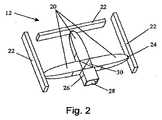
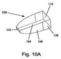
図2に拡大略斜視図で示されるLED光源システム12は、他のLEDベースのシステムに比較して、より小型のパッケージできわめて高い光束発散度を提供する。LED光源システム12は、それぞれの入射口24(右側のみに番号を付す)を略満たす関連するLEDダイに加えて、好ましくは矩形断面の、3つの非回転対称の誘電体CPC集光要素20を備える。LEDダイは、アレイまたは大きな表面の放射体の形態とすることができ、入射口24に位置し、高性能熱伝導体LED基板22(以下に詳述)に直接取り付けられる。CPC20は、良好な熱的および機械的性能に加えて、LED光源のスペクトル範囲にわたって低吸収である特性を有する、アクリル、ポリカーボネート、Zeonex等のような中実の誘電体材料で作製されることが好ましい。一般的に、LEDダイの表面と、対応するCPC集合光学要素20の入射口24との間には、シリコンゲルのような屈折率整合媒体が存在する。3つのCPC20の出力は、Xキューブ30に結合されるが、このキューブは、3色のビームを単一のビームとして収集して、矩形の出射口28の方へ導き、その後リレーレンズ14を経てDMD36上に結像する。周知のように、出射口28の近傍における出力は、さらに離れた遠方場となる近接場を表し、近接場は、従来では、光源およびそれを超える遠方場の直径の10倍の範囲内である。CPC20の出射口(図3の符号46を参照のこと)と、Xキューブ30のそれぞれの入射面との間のインターフェースは、以下に示されるように、CPC20の開口部を出射した全ての光がXキューブ30の寸法に閉じ込められるように、空気、または屈折率が十分に低い屈折光結合材料とすることができる。 The LED
スペクトルビーム結合器として機能するXキューブ30を出射した光は、DMD36上に直接結像するか、または光パイプ26によってさらに均質化することができる。光パイプ26の開口部28を出射した光は、次いでリレーレンズ14によってDMD36上に結像される。光パイプ26は、図に示されるように中空または中実の固体誘電体で構成することができる。中空反射体の利点は、表面に存在し得る不完全部が無く、DMD36上に再結像され、それによって、観察者が観察できるスクリーン44上に再結像されることである。また、下述するように、出射口28は傾斜させ易く、必要に応じてある程度の上下方向台形歪補正機能が得られる。中空光パイプの欠点は、反射のたびに有限の損失が存在することであり、この損失は、短い光パイプの場合は許容できるが、長い光パイプの場合はスクリーン上の総光電力に問題が生じる。 The light exiting the X-cube 30 functioning as a spectral beam combiner can be imaged directly on the
単一の中実誘電体の矩形CPC20の拡大図を図3の略斜視図に示す。出射口46は、CPC20の他のパラメータとともに、変調器36のエタンデュと整合するように設計される。変調器のエタンデュは、一般的に、その面積、立体受光角、および屈折率(一般的に空気)の2乗の積によって与えられ、一般的にmm2−ステラジアンで表される。出射口46は、DMD36と略同じアスペクト比を有する。寸法は、リレー14の倍率に依存する。一般的にLEDダイからの全ランバート放射プロファイルを収集するものと仮定すれば、CPC20のプロファイルは、両方の直交軸(すなわち、x−z面およびy−z面、z軸を長手方向の光軸とみなす)内にある複合放物面集光器であることが好ましい。したがって、CPCからの対称遠方場の角度に関して、CPC20の入射口24は、出射口46と同じアスペクト比を有する。CPCプロファイルの長さおよび形状は、2つの軸において異なる。したがって、短い方の寸法はより短い全長を有し、線52からエッジ50において出射面へ延在しなければならない。2つの直交軸におけるCPCの形状および長さは、最初に所望の出射角度および寸法を設定することによって決定される。標準CPCの式を用いることで、対応する入射寸法および長さを設定する。入射寸法は、入射矩形を画定するように組み合わせられ、CPCの長さの差異は、CPCの中実形状全体に到達するように、短い方のCPCプロファイルの長さから、長い方のCPCプロファイルまでの直線セクションを提供することによって補償される。CPCの4つのコーナー部での、すなわち対角線に沿ったCPCの形状は、単純に、直交面x−zおよびy−z内の2つのCPC形状の交点である。CPCの形状に到達するための計算は、関連パラメータおよびCPCの式を含んだ表計算を使用して好都合に行うことができる。An enlarged view of a single solid dielectric
光源12の出射口28の正反対のLED光源に対して、TRACEPRO光モデリングソフトウェアによって行った光線追跡を図4に示す。CPC集光器20の壁62によって反射された光線が、Xキューブ30に閉じ込められることによって、光ホモジナイザ26の入射口28に案内されているように示されている。Xキューブ30のコーティングは、それを通って真っ直ぐに導かれた波長、すなわち垂直に配向された図4のCPCからの波長を透過するように行われる。 FIG. 4 shows ray tracing performed by TRACPRO light modeling software for the LED light source opposite to the
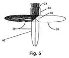
同様に、図5は、Xキューブ30の誘電コーティングに左側に反射して開口部28に向かう、LED光源およびCPC集光器20からの出射を示す図である。この光はまた、光をパイプするXキューブ30にも閉じ込められる。本発明のXキューブ30は、発散ビームを収容するように極めて大きくなければならない標準のXキューブと比較して、非常にコンパクトなシステムを提供する。これはシステム全体のコストおよびサイズを低減する。 Similarly, FIG. 5 is a diagram showing the emission from the LED light source and the
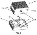
図6を参照すると、その上方には完全なLED投影光源モジュール70の略斜視図が示され、図の下方にはその断面図が示されている。LED基板22は、はんだ付け、ブレージング、サーマルグリスなどによって熱的に放熱板76に取り付けられ、CPC集光要素20の面の上部および下部の両方に位置する光学要素を挟む。放熱板76は、銅、アルミニウム、ダイヤモンド、包埋黒鉛のような複合材、またはヒートパイプのような高熱伝導率の材料であることが好ましい。ヒートパイプの場合、ウィック構造を用いたタイプのものとは対照的に、毛細管を組み込んだタイプのものは、あらゆる配向での動作を提供する。放熱板74によって、動作条件に基づいて対流または強制空冷することができる。面板72は、正面を覆って出射口28だけを露出させる。 Referring to FIG. 6, a schematic perspective view of a complete LED projection
LEDの外部量子効率を増加させる方法における最近の発達により、上述のように屈折率整合が無い場合でも、非常に高い抽出効率が得られる。マイクロレンズアレイ、マイクロプリズムアレイ、角度ファセッティング、フォトニック格子などのような、これらの方法を使用する前に、LEDの立方ジオメトリが、内部全反射(total internal reflention:TlR)によるLEDダイ内への光の閉じ込めをもたらした。外部量子効率は、TIRに打ち勝つための封入剤の屈折率のほぼ2乗に向上した。したがって、歴史的に、LEDはカプセル化による恩恵を受けている。外部量子効率を増加させるための機能を組み込んだLEDのこれらの最近の改善では、カプセル化による恩恵は比例的に少ない。したがって、DMDなどのエタンデュに整合するように改善したこのようなLEDの出力をCPCに結合させる改良を提供して、このようなLEDからより高い有効出力を利用する。 Recent developments in increasing the external quantum efficiency of LEDs result in very high extraction efficiencies even in the absence of refractive index matching as described above. Prior to using these methods, such as microlens arrays, microprism arrays, angular faceting, photonic gratings, etc., the cubic geometry of the LED is into the LED die with total internal reflection (TlR). Brought light confinement. The external quantum efficiency was improved to approximately the square of the refractive index of the encapsulant to overcome TIR. Thus, historically, LEDs have benefited from encapsulation. With these recent improvements in LEDs that incorporate features to increase external quantum efficiency, the benefits of encapsulation are proportionally low. Thus, an improvement is provided that couples the output of such an LED improved to match an etendue such as DMD to the CPC to take advantage of the higher effective output from such an LED.
周知のように、エタンデュは基本的に、デジタルマイクロミラー(DMD)または反射型液晶パネル(LCOS)デバイスを介して結像することができ、デバイス面積、制限立体受光角、および媒体の屈折率の2乗の積によって与えられる。一般的に、変調デバイスは空気に使用され、一般的に、これらのデバイスは、少なくとも1つのアジマスにおいて、12°の受光半角を有する。したがって、より高性能なデバイスの場合、例えば中空集光要素を用いることによって、LEDダイと集光要素との間の媒体として空気を用いたLED投影システムを設計した方が良く、したがって、より大きな有効LEDダイのサイズおよび、より高い有効光電力をもたらす不変のエタンデュによる恩恵を受ける。故に、屈折率整合を用いない利点は、外部量子効率を増加させるように機能を組み込んだことで、屈折率整合によってその出射が著しく増加しない理想的なダイの固定出射口の輝度が約2倍になることである。したがって、中空反射体は、理想的なダイの誘電体充填反射体よりも約2倍の利益が得られる。実用上、LEDはまだ理想的でないので、利益は2倍未満であるが、それでも有意となり得る。例えば、新しいCREE EZ900ダイは、カプセル化しても、その出力は約20%しか増加しない。したがって、理想的な中空反射体を使用することによる、光束発散度(固定LEDダイの電流密度に対して)の正味の増加は160%である。しかし、幾らか古いCREE XBおよびXT LEDダイの構成では、それでも、代表的な屈折率1.5の封入材料で屈折率整合したときには、光束発散度が約2倍に増加する。このように、これらのデバイスは、理想には程遠いものである。しかし、EZ CREEダイの場合、中空反射体の使用に有効である。EZ1000での中空反射体の使用は、入力電力が誘電体封入反射体の2倍となる点においては、コストのかかるものとなるが、より高いスクリーン上の輝度の達成に歓迎されるトレードオフであることに留意されたい。 As is well known, etendue can basically be imaged through a digital micromirror (DMD) or a reflective liquid crystal panel (LCOS) device, with device area, limited stereo acceptance angle, and the refractive index of the medium. Is given by the product of the squares. In general, modulation devices are used for air, and typically these devices have a light receiving half angle of 12 ° in at least one azimuth. Thus, for higher performance devices, it is better to design an LED projection system using air as the medium between the LED die and the light collection element, for example by using a hollow light collection element, and thus a larger Benefit from the size of an effective LED die and an unchanging etendue that results in higher effective optical power. Therefore, the advantage of not using refractive index matching is that the function of increasing the external quantum efficiency is incorporated, and the brightness of the fixed exit of an ideal die that does not significantly increase its output due to refractive index matching is approximately doubled. Is to become. Thus, a hollow reflector provides about twice the benefit over an ideal die dielectric-filled reflector. In practice, LEDs are not yet ideal, so the profit is less than twice, but can still be significant. For example, a new CREE EZ900 die increases its output by only about 20% when encapsulated. Thus, the net increase in luminous flux divergence (relative to the current density of the fixed LED die) by using an ideal hollow reflector is 160%. However, some older CREE XB and XT LED die configurations still increase the luminous flux divergence by a factor of about two when index matched with a typical refractive index 1.5 encapsulant. Thus, these devices are far from ideal. However, the EZ CREE die is effective for the use of a hollow reflector. The use of a hollow reflector in the EZ1000 is costly in that the input power is twice that of the dielectric encapsulated reflector, but at a trade-off welcomed in achieving higher screen brightness. Note that there are.
より大きなダイの効率は、通常は、より小さなダイよりも大きい。例えば、CREE EZ1000ダイは、EZ290ダイの相当面積のほぼ2倍効率的である。その理由は、電極とダイのエッジとの間のデッドスペースが、大きなダイでは比例的に少なくなるという事実に関連する。加えて、大きなダイおよび小さなダイのボンディングパッドの寸法は類似しているので、大きなダイのボンディングパッドに必要なスペースが比例的にかなり少なくなる。大きなダイの効率の増加は、エピタキシャルリフトオフ法を用いたトゥルートップ(true top)放射デバイスに当てはまる。UEC(Epistar)赤色ダイ、およびCREE EZタイプのダイのようなこれらのデバイスは、もはやバルク放射体ではない。したがって、それらは、例えばCREE XB900がそうなるように、より大きなバルク放射体内の内部吸収の増加による問題を生じない。このように、一般的には、最新の上部放射LEDにより大きなダイを使用するほうがさらに良い。また、より大きなフォーマットのダイをワイヤボンディングおよびダイ接着することはより容易であり、信頼性が向上し、システムのコストが下がることになる。 The efficiency of a larger die is usually greater than a smaller die. For example, the CREE EZ1000 die is approximately twice as efficient as the equivalent area of the EZ290 die. The reason is related to the fact that the dead space between the electrode and the edge of the die is proportionally less for large dies. In addition, because the dimensions of the large and small die bonding pads are similar, the space required for the large die bonding pads is proportionally significantly reduced. The increase in large die efficiency applies to true top radiating devices using epitaxial lift-off techniques. These devices such as UEC (Epistar) red dies and CREE EZ type dies are no longer bulk radiators. Thus, they do not cause problems due to increased internal absorption within larger bulk radiators, such as CREE XB900. Thus, it is generally better to use a larger die for modern top-emitting LEDs. Also, larger format dies are easier to wire bond and die attach, improving reliability and lowering system cost.
理論的には、円形断面の複合放物面集光器の入射口に入射する光の96%は、設計角度の範囲内で出射口を出射するので、完全な集光器に非常に近いものとなる。しかし、デジタルマイクロミラーデバイス(DMD)および反射型液晶パネル(LCOS)のような光変調デバイスは、一般的に矩形である。したがって、円形断面の集光器を使用した場合は、領域内に不整合が生じる。例えば、XGAフォーマットの変調器を用いて、XGA開口部を刻み込んだ円形断面の集光器を用いた場合、約40%の光が矩形の開口部に入らないために無駄になる。これにより、更なる発熱および電力の浪費がもたらされる。熱放散を有限と仮定した場合は、ダイの温度がより高くなり、性能および寿命の両方を低下させる、代替的な手法では、矩形断面の集光器を使用している。このような集光器はまた、両方の軸における出射角が同じ公称角度となるように、2つの異なる仕様の複合放物面集光器(1:1ではないアスペクト比とする)も使用することができる。これにより、2つの軸内に異なる有効長の矩形CPCがもたらされる。なお、図3および7に示されるように、長さの短いデバイスは、平行な壁によって延在させて1つの複合集光器を作製することができる。ここでは、対角線の方へ進むスキュー光線は、約87%の光しか設計角度に閉じ込められない。しかし、これは、所与の光束発散度に対して、ダイ面積を減じ(関連すること巣が下がる)、ダイ接合部の温度を下げることになるので、適切なトレードオフである。集光器の形状は、刻面、複数のスプラインフィット、または高次多項式などを含む他の形状によって近似させることができる。 Theoretically, 96% of the light entering the entrance of a compound parabolic concentrator with a circular cross-section exits the exit within the design angle and is very close to a perfect concentrator. It becomes. However, light modulation devices such as digital micromirror devices (DMD) and reflective liquid crystal panels (LCOS) are generally rectangular. Therefore, when a circular cross-section collector is used, mismatch occurs in the region. For example, when a XGA format modulator is used and a concentrator having a circular cross-section with an XGA opening is used, approximately 40% of the light is wasted because it does not enter the rectangular opening. This leads to further heat generation and power waste. Assuming that heat dissipation is finite, an alternative approach that uses a higher die temperature and reduces both performance and lifetime is using a concentrator of rectangular cross section. Such a concentrator also uses two different specification compound parabolic concentrators (with an aspect ratio other than 1: 1) so that the exit angles in both axes are the same nominal angle. be able to. This results in rectangular CPCs of different effective lengths in the two axes. Note that, as shown in FIGS. 3 and 7, a short device can be extended by parallel walls to make one composite concentrator. Here, only about 87% of the skew rays traveling toward the diagonal are confined at the design angle. However, this is an appropriate tradeoff because for a given flux divergence, the die area will be reduced (the associated nest will be reduced) and the die junction temperature will be lowered. The shape of the concentrator can be approximated by other shapes including facets, multiple spline fits, or higher order polynomials.
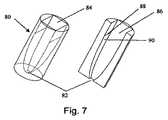
上述の円対称の複合放物面集光器は、非結像光学要素のエッジ光線原理から導出されたものであり、ほぼ理想的な性能を有することが示されている(High Collection Nonimaging Optics、W.T.Welford and R.Winston、Academic Press、1989)。しかし、複合楕円型集光器(compound elliptical concentrator:CEC)および複合双曲面型集光器(compound hyperbolic concentrator:CHC)のような、類似した近接場および遠方場性能をもたらすことができる他の形状が存在する。特に、その出射口の視野レンズと併用した複合双曲面型集光器は、長さは非常に短いが、CPCに極めて類似した近接場および遠方場性能を有することが知られている。このCHC/視野レンズの設計およびその派生物は、標準のCPCに対して長さが非常に短い、理想に近い集光器になり得る。これは、CPCを非常に長くすることができる、低開口数デバイスに特に有用である。これらのタイプの光学要素は、LEDダイまたはダイアレイとの併用が有用である。近接場および遠方場における均一性を達成し、最大エタンデュを維持するためには、光学要素の入射口を略満たしておくことが重要である。投影システムは、デバイスのエタンデュによって本来的にスループットが制限されるので、最適な性能の達成には、システム全体にわたってそのエタンデュを維持することが重要である。図7は、不等長かつ不等幅の入射口82を備えた中空反射CPC80を示す図である。寸法がより短くなることで、その関連する軸においてCPCプロファイル90の長さが比例的に短くなる。短いCPC90の出射口に接する平行側部88は、長いCPC86の長さまで延在する。このようにして、両方の軸は、同じ出射角を有し、それによって対称な遠方場が発生するように設計される。 The above-described circularly symmetric compound parabolic concentrator is derived from the edge ray principle of non-imaging optical elements and has been shown to have nearly ideal performance (High Collection Nonimaging Optics, WT Welford and R. Winston, Academic Press, 1989). However, other shapes that can provide similar near and far field performance, such as compound elliptical concentrators (CEC) and compound hyperbolic concentrators (CHC) Exists. In particular, a compound hyperboloidal concentrator used in combination with a field lens at its exit is known to have near field and far field performance very similar to CPC, although it is very short in length. This CHC / field lens design and its derivatives can be near-ideal concentrators that are very short in length to standard CPC. This is particularly useful for low numerical aperture devices where the CPC can be very long. These types of optical elements are useful in combination with LED dies or die arrays. In order to achieve near-field and far-field uniformity and maintain maximum etendue, it is important that the entrance of the optical element is substantially filled. Since projection systems are inherently limited in throughput by the device's etendue, it is important to maintain that etendue throughout the system to achieve optimal performance. FIG. 7 is a diagram showing a hollow
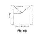
図8Aは、エッジ付近のより高い光束を示す、誘電体または中空矩形CPCに一般的な近接場の分布の三次元線図である。図8Bは、図8Aの等高線図の中央を通る直交軸XおよびYに沿った変化の二次元線図である。エッジ付近のより高い光束は、スクリーン上の輝度の場のエッジに向かう低下を打ち消すことによって有効に使用することができ、図1の一般的に広角の投影光学要素16のコサインθロールオフによる一般的なスクリーン上の損失である。図3の誘電体充填CPCは、類似した遠方場特性を有する。 FIG. 8A is a three-dimensional diagram of the near-field distribution common to dielectrics or hollow rectangular CPCs, showing higher luminous flux near the edges. FIG. 8B is a two-dimensional diagram of changes along orthogonal axes X and Y through the center of the contour map of FIG. 8A. Higher luminous flux near the edge can be used effectively by counteracting the drop in luminance field on the screen toward the edge of the edge, and is generally due to the cosine θ roll-off of the generally wide-angle projection
円形断面のCPCとは対照的に、図7の矩形断面のCPCは、図9Aおよび9Bに示されるように、遠方場の設計角度の範囲内に光の約88%を保持する。図9Aは、矩形のCPCからの全遠方場を示す図である。図9Bは、設計角度(この場合は20°)の範囲内の光を表わす図であり、この光は、図1の投影レンズ16の円対称のストッパ40を通る。この正方形の遠方場の分布は、対角線付近で反射したスキュー光線の影響によるものである。それでも、このデバイスは、矩形の変調デバイスの入射口を整合させるよりもさらに無駄が少なく、この損失を上回って補償する。あるいは、投影光学要素は、矩形の遠方場に適応するように設計することができ、幾分大きなレンズになるが、スクリーン上の輝度が向上する。 In contrast to the circular cross-section CPC, the rectangular cross-section CPC of FIG. 7 retains about 88% of the light within the far-field design angle, as shown in FIGS. 9A and 9B. FIG. 9A is a diagram showing the total far field from a rectangular CPC. FIG. 9B is a diagram representing light within a design angle (in this case, 20 °), and this light passes through the circularly
Texas Instruments社製のDMDのような変調デバイスは、一般的に、ミラー偏光角が12°に制限される。一般通念では、このように照明角度を12°に制限するか、または照明と投影ビーム経路との間にオーバーラップを設ける。しかし、これはミラーの傾斜にしか当てはまらない。より大きな円錐角を直交方向に用いることが適切である。したがって、非対称遠方場によって、システムの総スループット、故にスクリーン上の強度を、一般通念を超えて増加させることができる。例えば、スクリーン上の輝度は、ミラー傾斜面に直交する軸にf/1.2の円錐体を使用することによって、2倍に増加させることができる。光源(図1の照明光学要素14および投影光学要素16)は、全てこの状態に整合させなければならない。非球面要素(プラスチックレンズを使用した場合は基本的に不要となる)は、低f/#のシステムによる収差の増加をバランスさせることを助ける。 Modulation devices such as Texas Instruments DMD are typically limited to a 12 ° mirror polarization angle. As a general rule, the illumination angle is thus limited to 12 °, or there is an overlap between the illumination and the projection beam path. However, this is only true for mirror tilt. It is appropriate to use a larger cone angle in the orthogonal direction. Thus, an asymmetric far field can increase the total throughput of the system, and hence the intensity on the screen, beyond common wisdom. For example, the brightness on the screen can be increased by a factor of two by using an f / 1.2 cone on the axis orthogonal to the mirror tilt plane. All light sources (illumination
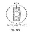
図10Aは、遠方場内に非対称分布を有する誘電体矩形のCPC100を示す図である。上述のように、Texas Instruments社製のDMDのような変調デバイスは、一般的に、12°に制限されたミラー偏光角を有する。出射口110は、DMDの寸法に整合される。しかし、入射寸法は、図10Bに示される遠方場分布を生成するように1つの軸において大きくなり、その結果、スクリーン上の輝度が100%増加する。これは、性能における有意な利益である。これによって、LEDベースのシステムを、従来教示されている限度をかなり超えて機能させることができる。 FIG. 10A is a diagram showing a dielectric
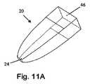
図11Aおよび11Bは、LED放射体の出力の全2πステラジアンを捕捉するように設計された矩形開口部のCPCと、全半球未満の幾らかの有限角度まで放射された光を捕捉するように設計されたものとを比較した図である。これは、WelfordおよびWinstonによって一般的な形態で述べられているが矩形CPCの場合まで拡大されるように、シータ対シータ(θ対θ)CPCを用いて達成することができる。図11BのCPC120のセクション126は、インターフェースにおいて放物面プロファイルに接する直線のセクションを表す。その結果、入射口のサイズが大きくなり、図11Aに示されるCPC20の開口部24と比較して、図11Bの開口部124からの光束発散度が増加する。実際に、LEDダイの法線からセクション126の円錐の設計角度より大きな角度で開口部124に入射する光は、設計角度よりも大きな出射角度に結合される。当業者は、セクション126に類似した円錐セクションは、回転対称のCPCセクションとともに容易に使用することができ、LEDが屈折率適合されていない中空の回転対称集光器と略同じ性能を有する、中実の集光光学要素を提供することができると認識されよう。 11A and 11B are designed to capture a CPC with a rectangular aperture designed to capture the full 2π steradians of the output of the LED emitter and light emitted to some finite angle less than the full hemisphere. It is the figure which compared with what was done. This can be achieved using theta to theta (θ to θ) CPC as described in general form by Welford and Winston, but extended to the case of rectangular CPC.
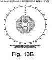
図12は、同じ長さの図4の矩形CPC20と同じ入射および出射口を備えた直線の先細部を示す図である。図13Aは、先細部に対する遠方場の分布が、CPC20の設計角度と比較して、20°の設計角度にあまり拘束されていないことを示す図である。図13Bに示される20°の範囲内では、光の67%しか投影レンズ16の開口絞り40を通過しない。したがって、矩形のCPCは、同じ長さの真っ直ぐな先細部に対して、30%を超える良好な性能を有することが示される。 FIG. 12 is a diagram showing a straight taper with the same entrance and exit aperture as the
図14は、共通の要素が元の同一性を保持する、図2のLED投影光源の別の結合の実施形態130を示す図である。ここでは、LEDダイまたはダイアレイは、(代表的な)高熱伝導性基板132に取り付けられ、CPC20の入射口24に結合され、円錐入射セクションの有無に関わらず中実または中空とすることができる。最左端のCPC20の出力は、導光プリズム138に入射する。光は、高反射率コーティングでコーティングされた138の斜辺によって90°反射される。図2のプリズム30の場合のように、プリズムおよび矩形のガラスセクション138、140、142、143、144、146、148、134、および136は、本来のパッケージングおよびコスト的に優位なコンパクトなサイズを維持するように、TIRを使用して、それらの入射寸法の範囲内に光を光パイプする。3色のLED光源のCPC20のそれぞれの出射口46と、出射口28との間の全光学経路は、類似した近接場の強度パターンおよび光の均質化を保持するように、光パイプ134および136によって略同じになっている。最左端のCPC20とプリズム138との間のスペース、およびプリズム138と中実の矩形ライトパイプセクション140との間のスペースは、空気かまたは屈折率媒体であり、最左端のCPC20からの光のTIRが反射傾斜面に反射する前にプリズム138に拘束され、傾斜面に反射した後にプリズムに拘束されるように十分小さいことが重要である。それ以外ならば、CPC20を出射した光の一部は、140および142の上面を通って透過されてしまうか、またはCPC20に再入射して、CPC20からの制限角度に保持されないことになる。同じ要件は、中央のCPCおよび矩形光パイプ144のプリズム143に対しても当てはまる。これはまた、ホモジナイザ26が中空ではなく中実の場合、プリズム148およびホモジナイザ26も当てはまる。図14の実施形態では、図2の導光Xキューブ30は、2つの別個の2色性波長依存の反射コーティングに置き換えられ、これらは、中央のCPCに対するプリズム142および143と、出射口28に最も近い右側のCPCに対するプリズム146および148との間に配置される。必要に応じて2色性のコーティングが透過または反射するように適切に設計されていれば、赤色、緑色、および青色(または他の色)のLED光源の特定の機構は重要ではない。あるいは、CPC20は、同じ方向または同じ面を向いている必要は無い。それらは、スペースおよび熱的な考慮に対して、必要に応じて互いに対向させるか、または直交させて配置することができる。同様に、プリズム138を排除することで、最左端のCPCがプリズム142に直接入るようにすることができ、それによって、プリズム138および光パイプ140が排除され、また、光パイプ134および136の長さの要件が軽減される。加えて、蛍光体または他の波長変換要素をLEDダイ全体に用いて、標準のLEDダイでは容易に利用できない波長およびスペクトル帯域幅を得ることができる。例えば、緑色のLED光は、青色のLED励起と緑色蛍光体とを組み合わせることによって発生させることができ、図33に示される人間の眼の明所視感度曲線のピークにより厳密に整合する。 FIG. 14 is a diagram illustrating another
中空のCPC集光要素を使用する利点は上述のとおりであるが、これらは、屈折率整合による抽出効率の増加がそれほど重要でない場合にのみ、LEDに対して適切に機能する。LEDダイシステム150からより多くの光を抽出する方法を図15Aおよび15Bに示し、ベアのLEDダイ(全体的に152で示される)は、単一体よりも大きな屈折率(一般的に1.5)のシリコンのような、低吸収媒体154によって整合的にカプセル化される。LED152から封入材料154へ出射することができる光は、続いて封入材料−空気の境界面において部分的に内部全反射(TIR)される。TIRによって封入材料154から空気中に出射しないようにしたLEDの放射は、次いでダイ表面へ反射される。LEDの拡散反射率が約50%を超える場合は、封入材料−空気の境界面を介して透過される角度スペース内で拡散的に反射したLED表面上に当たる光の一部として、空気中に抽出される光が純増加する。したがって、屈折率整合媒体に抽出された増加した光は、順方向に効果的に結合する、すなわちリサイクルすることができる。一例として、LEDの拡散反射率が60%で封入材料の屈折率が1.5の場合、空気への光の抽出が約20%以上に増加するが、これは封入材料の存在の存在しない状態で生じる。層の厚さは数10ミクロンあれば良く、したがって、コンフォーマルコーティングとしてしか機能しない。この手法は、図7に示される中空の反射体を使用することによって有効な利益が増加する。 The advantages of using hollow CPC concentrating elements are as described above, but they work properly for LEDs only when the increase in extraction efficiency due to refractive index matching is not as important. A method for extracting more light from the
図16Aおよび16Bを参照すると、矩形CPCの別の実施形態160が示され、図3のCPCの水平軸と垂直軸との間の集光要素の形状は、水平から垂直に長手方向に(すなわち、表面および光軸を通る子午面において)連続的に変化するCPCの形状と略同じである。166、168、170、および172によって表されるポイントは、異なる形状のプロファイルの全てのエンドポイントであるが、CPCの形状のそれぞれである。したがって、対角線に沿った方向の角度で、例えばCPCのエンドポイント166を通る角度、およびCPCの水平エンドポイント170と垂直エンドポイント172との間の、CPCのエンドポイント166で表される角度にあっても、その形態はCPCの形態である。これは、図3のCPCの単純な矩形断面によって導出される光学要素となり、矩形ではなく略円形の遠方場を生成する。したがって、図16Aおよび16Bの複合CPCでは、矩形の近接場および略円形の遠方場が得られ、図3のものよりも約10%スクリーン上の輝度が向上する。この手法では、中実または中空の光学要素の形態とすることができる。 Referring to FIGS. 16A and 16B, another
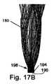
図17Aおよび17Bは、図11Bの形態の中実のCPC180を示す図であり、予混合ホモジナイザ198が、LEDダイまたはダイアレイとCPCの入射口184との間に配置される。この矩形断面の光パイプまたはホモジナイザ198は、CPC180の入射口184の寸法に整合する。図17Bに示される光線は、LED196と入射口186との間の屈折率整合媒体の有無に関わらず、この構成を使用できることを示している。また、中空のCPCの利益は、図17Aに示されるように、円錐セクション188によって境界を成す中実のCPCを使用することによって実現することができ、事実上、中空のCPCで実現できるところまで入射口184を開口する。実質的に、これは、CPCプロファイルと混合した円錐セクションを提供することによって、入射端部で変化させたCPCから成る混成設計である。 FIGS. 17A and 17B show a
これは、以下によって理解することができる。基本的な形態の立体エアスペース型CPCは、屈折率整合を前提に設計されている。しかし、194の近傍でLED光源196を出射した光線の屈折によって(図17Bを参照のこと)、この光線の広がりは、CPC180の誘電媒体内の半球のよりもはるかに小さい。したがって、屈折率適合していない無変更の形態のCPCの出射角度は、設計角度未満である。混合円錐のセクション188を備えたCPCを変化させることによって、入射寸法の増加に対する角度の増加が所望の角度スペースを充填するように角度が広げられる。このような混成集光器180では、角度および寸法に関する下流の要件を用いて、入射口のサイズおよびジオメトリの寸法に到達するように、誘電体材料の中実CPCを設計している。通常、これらの寸法は、角度およびサイズに関して同じ下流の要件に一致する中空設計のものよりも小さい。しかし、より大きなLEDの利点は中実の設計に求められるものであるため、その入射口は、入射面からエアスペースをとった、より大きなLEDを収容するように改良される。次いで、接点においてCPCプロファイルと交差するように、他のより大きなLEDのエッジから直線を描画する(図17Aの190を参照のこと)。その結果、エアスペース型および他の大きなサイズのLEDの利点を活用することによって、中空のものの性能を模倣した中実の混成集光器設計が得られる。 This can be understood by: The basic three-dimensional air space type CPC is designed on the assumption of refractive index matching. However, due to refraction of the light emitted from the LED
198の均質化の効果によって、実際のLEDダイの出射の均一性が向上し、電極およびワイヤボンディングの存在による均一な空間的出射が無い。また、CPC180の入射口184に入射する前に光を混合することによって、LEDダイと入射または出射口186との間の精度の影響も最小限に抑えられる。この光学要素、CPC、およびホモジナイザ198は、容易に一体型に成形することができる。図7の中空CPCの光学要素を覆う非屈折率適合の中実の集光要素の別の利点は、反射コーティングが不要であること、およびCPCの底部が寸法的にワイヤボンディングを妨げないことである。非屈折率適合の場合の入射口186のフレネル損失は、中空CPC上に被着させなければならない実際の反射コーティングによって生じる反射損失によって相殺される。 The homogenization effect of 198 improves the emission uniformity of the actual LED die and there is no uniform spatial emission due to the presence of electrodes and wire bonding. Also, by mixing the light before entering the
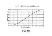
図17Aの混成集光器の利益は、混合された円錐部分188を使用する効果を理解することによってより完全に理解することができる。上述のように、標準の円形または矩形のCPCは、半球(2πステラジアン)にわたって光源から出射されたエネルギを受け取り、WelfordおよびWinstonのエッジ光線原理を用いて、エネルギが特定の設計角度でほぼ理想的な効率で放射される反射体を形成する。代表的なLEDダイの出力は、略ランバートである。すなわち、放射された光束は、角度のコサインとして表面法線から減衰し、総放射光束は、図18に示されるように、表面法線からの開光角度のコサイン2乗の積分に比例する。したがって、表面法線から離れた角度は、総集積光束にはほとんど寄与しない。 The benefits of the hybrid concentrator of FIG. 17A can be more fully understood by understanding the effect of using a mixed
図19は、非結像集光器からの光束発散度は、比例的に光束が少ない高角度を除外することによって増加させることができる。これは、立体角が小さくなることによって、(一定の電流密度に対して)放射光源の面積が比例的に減少するように、一定のエタンデュを前提としている。面積の増加による利益は、高角度を除外することによって収集した光束の損失よりも速く増加する。しかし、面積の増加は、相対的な入力電力の増加をもたらす。相対電力曲線は、60°の近傍に屈曲点があり、これは、集光器からの光束発散度の50%の増加に相当する。集光要素の設計は、WelfordおよびWinstonによって述べられているように、角度シータ対シータの集光器となり、図17Aの改良型CPC180は、特定の設計角度での直線円錐への接線を成すが、図3、7、10A、11A、および11Bに示される形態の矩形のCPCの場合に拡大される。60°の開光角度設計ポイントは、非線形に増加する電力と光束発散度の漸近的増加との間の適切なトレードオフである。 FIG. 19 shows that the divergence of the light beam from the non-imaging collector can be increased by excluding the high angle where the light beam is proportionally smaller. This presupposes a constant etendue so that the area of the radiation source decreases proportionally (relative to a constant current density) as the solid angle decreases. The benefits of increased area increase faster than the loss of collected light flux by excluding high angles. However, the increase in area results in an increase in relative input power. The relative power curve has an inflection point in the vicinity of 60 °, which corresponds to a 50% increase in luminous flux from the collector. The concentrator design is an angle theta to theta concentrator, as described by Welford and Winston, while the
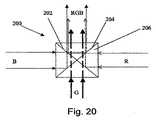
図20乃至27は、一般的に赤色、緑色、および青色の光を、それぞれの集光要素から、DMD変調器36などの上に結像することができる共通のビームに結合するための、別の実施形態を示す図である。 FIGS. 20-27 show alternatives for combining generally red, green, and blue light from their respective collection elements into a common beam that can be imaged onto a
図20を参照すると、Xキューブ200が概略的に示されており、緑色の波長は、一般的に方向を変えないキューブを介して透過され、赤色および青色の波長は、出射面へ向かってそれぞれの表面202および204で反射する。この全般的な手法は過去に用いられたものであるが、サイズ低減のための光パイピングに対する更なる要件は無い。図3のシステムは、この基本的手法を改良したものであるが、さらにコンパクトであり、よって製造コストがより低くなる。 Referring to FIG. 20, an
図21は、4つの別個の2色性ビームスプリッタ212、214、216、および218を備えたXプレート210の形態のXキューブの一変形例を示す図であり、図20のXキューブとほぼ同じように、異なる色のビームの方向を換えるように構成される。 FIG. 21 shows a variation of the X-cube in the form of an X-plate 210 with four separate
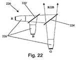
XキューブおよびXプレートの別の結合システムを図22に220で示すが、複雑さおよびコストがより低くなることが見込まれる。図に示されるように、R、G、およびBビームを発生させる3つのCPC226および2つのビームスプリッタ222および224がある。緑色のCPC226のそれぞれのビームスプリッタ224からの距離は、経路を均一にするために、他の2つのCPCにおける距離よりも長くなっている。図1のリレーシステム14の複雑さを低減する方法では、単色性のリレーに対して全ての色光源がDMD36の面で重なるように、図1のLED照明光源28
の出射口との相対的な光学経路の差異を調整する。これはリレーの複雑さを低減し、よって更なる無色化が不要となりコストが削減される。同じ手法を、図22のシステムに使用することができる。Another coupling system for X-cubes and X-plates is shown at 220 in FIG. 22, but is expected to be less complex and cost. As shown in the figure, there are three
The difference in the optical path relative to the light exit is adjusted. This reduces the complexity of the relays, thus eliminating the need for further decolorization and reducing costs. The same approach can be used for the system of FIG.
図23を参照すると、角度によって変化する波長依存透過のビーム結合要素230が示されている。これは透過型回折格子を用いて達成することができ、例えば、緑色の波長は、青色および赤色ビームによって囲まれてほとんど逸脱せずに透過させることができ、適切な角度で偏向される。あるいは、要素230は、音響光学偏向器または、2または3ガラスプリズムとすることができる。2ガラスプリズムは、全偏向角を導入し、3ガラスプリズムは、中央の周波数帯での偏向をゼロにするように設計することができる。格子の効率によるスループット、およびスペクトル拡散には制限があるが、これは、ビームを組み合わせる非常にコンパクトな方法を表すことができる。 Referring to FIG. 23, a wavelength dependent transmission
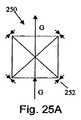
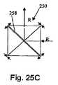
図24AおよびB、ならびに図25A、B、およびCは、単一のDMD投影システムの色順序要件に特に関連するビームスプリッティングの方法を示す図である。図24Aに示されるように、ビームスプリッタ240は、2つの分離可能な直角プリズムの半割り部244を備える。プリズムの半割り部244は、それらの共通斜面でプリズム間に間隙を形成して、このインターフェースに沿ったプリズム同士の光学的接触を無効にするように、互いに離れることができる。プリズム244の間の距離は、図24Bの構成に概略的に示されるように、約数ミクロン乃至数十ミクロンとされ、例えば赤色と青色を組み合わせたビームを、90°の偏向角で組み合わせて出射の方向に反射するように機能する。図24Aの構成は、2つのプリズムを光学的に接触させた場合、すなわち、約1ミクロン以下の範囲内で離れている状態を示す。この手法は、内部全反射は変動するという原則に基づくものであり、第1の半割りのプリズムを出て第2の半割りのプリズムに入射する光の電磁場のエバネセントテールの範囲内に2つの面がある場合に、光は、2つのプリズム間の境界面を介して透過される。この分割は、駆動電力の関数として拡大または縮小する特性を有する圧電スタック変調器によって変調されることが好ましい。これは、適切な平衡のために、一般的に1つの面内の3つの位置に用いられる。デバイスを迅速に調整する必要があり、プリズム間の空気が制限因子となる場合、そのデバイスは、真空にした気密パッケージ内に配置することができる。 FIGS. 24A and B, and FIGS. 25A, B, and C illustrate beam splitting methods that are particularly relevant to the color order requirements of a single DMD projection system. As shown in FIG. 24A, the
図25A、B、およびCは、図2のものに類似した3つの位置のデバイス250を示すが、図に示されるように4つの直角プリズムを備える。プリズムは、図に示されるように作動して、必要に応じて光を右または左から透過または反射する。有意な損失はフレネル損失のみであり、良好な反射防止コーティングを用いて透過効率を100%に近づけさせているので、透過効率は90%台まで高められる。図25Aは緑色を透過する間隙が無いものに対応し、図25Bは青色を透過する間隙256に対応し、図25Cは赤色を透過する間隙258に対応する。 FIGS. 25A, B, and C show a three
図26を参照すると、中心軸264の周りをガルバノメータまたはサーボモータによって作動する傾斜ミラー260が示されている。ミラー260の角度変調は、その角度を迅速に調整して、複数色のLEDからの光を順々に結合させるように構成されるが、これは色順序システムに理想的である。ガルバノメータはサブミリ秒の時間的尺度で動作することができ、LED投影システムに適している。 Referring to FIG. 26, there is shown a
図27は、回転スキャナ270の形態の別の結合の実施形態を示す図である。回転ミラー276は、軸278の周りを回転して1度に1つの色をアドレスする。この手法には、複数色の光源にも拡大することができ、LED光源を全て同じ面内に配置することができ、熱的な設計を簡素化するという利点もある。 FIG. 27 is a diagram illustrating another coupling embodiment in the form of a
図28は、LED基板の温度を管理する従来技術の手法の代表例である。LED基板290は、LEDダイ298および基質310との間に1つ以上の材料層304、306、308、および312を有する高導電率の基板310を備える。これに対して、図29にはLED基板320が示され、レーザアブレーション、機械加工、またはエッチングプロセスを用いて、図30に示されるように熱的性能が大幅に改善されるように、LEDダイ328を高熱伝導率の基板330上に直接取り付けることができる。図30は、入力電力の関数として、2つの場合の光出力の比較を示す線図である。ケース1は、図29に示されるように、ダイを基板に直接載置する場合で、ケース2は、厚さ0.003”の誘電体材料の中間層があり、図28ほどは不適当ではないがこれに類似する場合である。どちらの場合も、1ワットのCREE XB900ダイを積分球内で測定した。1ワットの公称電力における2つの場合の差異は、無視してよい。しかし、LED投影システムおよびキセノンランプ置換に必要な、より高い電流密度では、その差異は重要である。誘電体の場合は、約3ワットの入力電力での性能にわたって性能を発揮する。しかし、LEDを直接取り付けた場合は、高い駆動電力で200%乃至300%の出力を達成する。これは、投影システムおよびキセノンアークランプ置換システムにとって大きな利益である。 FIG. 28 is a representative example of a conventional technique for managing the temperature of the LED substrate. The
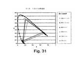
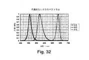
図31は、標準的な短アークランプと比較して、LEDを使用することによって達成することができる色域を示す図である。代表的な青色、緑色、および赤色LEDの測定スペクトルを図32に示す。LED投影光源内の総ルーメンに対する相対的な寄与は、図33に示されるように、大部分が、眼の測光反応によって緑色のチャネルに由来する。 FIG. 31 is a diagram showing the color gamut that can be achieved by using LEDs compared to standard short arc lamps. Measurement spectra of typical blue, green, and red LEDs are shown in FIG. The relative contribution to the total lumen in the LED projection light source is largely derived from the green channel by the eye photometric response, as shown in FIG.
図34は、青色、緑色、および赤色LEDダイの代表的な熱係数を示す図である。赤色は、青色(最も安定している)または緑色よりも温度に敏感であることが示され、緑色よりもわずかに不安定である。熱的性能における差異、および時間によるルーメンの維持における差異は、3つのLEDチャネルの光出力へフィードバックが必要である。モニタリング光ダイオードは、「チップオンボード」設計のLED上に容易に組み込んで、閉ループの輝度調節を提供することができる。 FIG. 34 is a diagram illustrating representative thermal coefficients for blue, green, and red LED dies. Red is shown to be more sensitive to temperature than blue (the most stable) or green and is slightly more unstable than green. Differences in thermal performance and maintenance of lumens over time require feedback to the light output of the three LED channels. Monitoring photodiodes can be easily incorporated on LEDs of “chip on board” design to provide closed loop brightness adjustment.
人間の眼は、眼の一時的な反応および非線形の輝度応答の持続性を利用して、より高い輝度の光を知覚することによってだまされる可能性がある。例えば、ある場合では50%のデューティサイクルで、別の場合では100%のデューティサイクルを保持して、ほぼ100Hzの周波数で光源を調整し、どちらの場合も層集積光が同じであった場合、最初の場合では、約30%輝度が増加したと認知する。この方法は、他のビジュアルシステムベースの製品に効果的に用いられ、また、背面投影のためのアプリケーションを有することができる。これは、従来のランプでは実用的でなかったが、LEDによって可能となり、容易に調整することができる。 The human eye can be deceived by perceiving higher brightness light using the temporal response of the eye and the persistence of a non-linear luminance response. For example, if the light source is adjusted at a frequency of approximately 100 Hz with a 50% duty cycle in some cases and a 100% duty cycle in other cases, the layer integrated light is the same in both cases, In the first case, it is perceived that the brightness has increased by about 30%. This method can be used effectively with other visual system based products and can also have applications for rear projection. This is not practical with conventional lamps, but is possible with LEDs and can be easily adjusted.
照明光学システムの課題のうちの1つは、変調デバイス(例えば、DMD)は、照明システムの軸に対して垂直ではないという事実である。これにより、キーストンおよび焦点深度の問題が生じる。このような影響は、キーストンを打ち消すように、図2の出射口28を傾斜させることによって減じることができる。他の方法には、傾斜および偏心させたレンズを使用することが挙げられる。これは、ある角度をなす誘電体光パイプが屈折によるビームの偏りをもたらすので、中空の反射体セクションにおいて最良に達成される。 One of the challenges of the illumination optical system is the fact that the modulation device (eg DMD) is not perpendicular to the axis of the illumination system. This creates keystone and depth of focus issues. Such an effect can be reduced by tilting the
照明システムの断熱化は、動作および輸送時の最高最低温度によっては必要となる場合がある。プラスチックの熱膨張係数に整合させる1つの方法は、ガラス充填物を使用することである。ガラスを充填したレンズおよびレンズハウジングは、プラスチックの熱膨張率を、LED基板の金属基板の熱膨張率に整合させることによって、実現することができる。 Insulation of the lighting system may be necessary depending on the maximum and minimum temperatures during operation and transportation. One way to match the coefficient of thermal expansion of the plastic is to use a glass fill. Glass-filled lenses and lens housings can be realized by matching the coefficient of thermal expansion of the plastic to the coefficient of thermal expansion of the metal substrate of the LED substrate.
本発明の構造および動作の詳細な説明およびその種々の実施形態に基づくことで、当業者には、他の改良を行うことが可能であり、そのような改良も添付の特許請求の範囲内であることが明らかとなるであろう。 Based on the detailed description of the structure and operation of the present invention and the various embodiments thereof, those skilled in the art can make other modifications, and such modifications are within the scope of the appended claims. It will be clear that there is.
Claims (34)
Translated fromJapanese所定のエタンデュおよびスペクトル出力を有する少なくとも1つのLED光源と、
該少なくとも1つのLED光源によって放射された光の実質的に全てを収集し、かつ、該LED光源と実質的に同じエタンデュのビームとしてそれを再放射する、少なくとも1つの非結像光学要素であって、該非結像光学要素は、入射口と、出射口と、該入射口から該出射口へ連続的に拡大する非回転対称の断面形状とを有し、該少なくとも1つのLED光源は、該入射口が該LED光源の出力によって実質的に均一に満たされるように、該にゅうしゃ口に、またこれを完全に横切って配置され、該少なくとも1つのLED光源の出力は、該非結像光学要素の形状によって導かれ、該少なくとも1つのLED光源と実質的に同じエタンデュであるが、該下流のアプリケーションの該エタンデュに実質的に一致するために、角度と寸法とが異なるビームとして、該出射口から現れる、非結像光学要素とを備える、照明装置。An illumination device that provides an output beam that matches the etendue of a downstream application,
At least one LED light source having a predetermined etendue and spectral output;
At least one non-imaging optical element that collects substantially all of the light emitted by the at least one LED light source and re-radiates it as a beam with substantially the same etendue as the LED light source. The non-imaging optical element has an entrance, an exit, and a non-rotationally symmetric cross-sectional shape that continuously expands from the entrance to the exit, and the at least one LED light source includes the Positioned at and completely across the inlet so that the entrance is substantially uniformly filled with the output of the LED light source, the output of the at least one LED light source is the non-imaging optical Guided by the shape of the element and having substantially the same etendue as the at least one LED light source, but with different angles and dimensions to substantially match the etendue of the downstream application. As the beam emerges from the exit port, and a non-imaging optical elements, the illumination device.
該第1の直線壁セクションおよび該第2のCPCセクションは、該固体非結像光学要素が、前記円錐セクションが無い場合に生じ得るよりも大きいLEDの出力を効率的に利用できるように、これらのセクションが共通接点を共有する境界面において接合する、請求項8に記載の照明装置。The solid non-imaging optical element comprises a first straight wall section starting from the entrance and a second section having the shape of a CPC and ending at the exit;
The first straight wall section and the second CPC section are such that the solid-state non-imaging optical element can efficiently utilize a larger LED output than can be produced without the conical section. The lighting device of claim 8, wherein the sections join at an interface sharing a common contact.
所定のエタンデュおよびスペクトル出力を有する少なくとも1つのLED光源と、
入射光を選択的に調整するためのデジタルデバイスであって、所与のエタンデュを有する、デジタルデバイスと、
該少なくとも1つのLED光源によって放射された光の実質的に全てを収集して、該LED光源と実質的に同じエタンデュの空間的に均一なビームとして再放射する、少なくとも1つの非結像光学要素であって、該非結合光学要素は、入射口と、出射口と、該入射口から該出射口へ連続的に拡大する非回転対称の断面形状とを有し、該少なくとも1つのLED光源は、該入射口が該LED光源の出力によって実質的に均一に満たされるように、該入射口に、またこれを完全に横切って配置され、該少なくとも1つのLED光源の出力は、該非結像光学要素の形状によって導かれ、該少なくとも1つのLED光源と実質的に同じエタンデュであるが角度が異なり、該デジタルデバイスのエタンデュに実質的に一致する寸法を有するビームとして、該出射口から現れる、少なくとも1つの非結像光学要素と、
ビデオ画像を形成するように該非結像光学要素からの近接場を該デジタルデバイス上に結像するリレーレンズと、
そこに形成される画像を観察するスクリーンと、
該観察スクリーン上に形成されたビデオ画像を該観察スクリーン上で観察できるように、該デジタルデバイスを調整しながら、該デジタルデバイスを該スクリーン上に投影する投影レンズと
を備える、投影装置。A projection device for forming a video image,
At least one LED light source having a predetermined etendue and spectral output;
A digital device for selectively adjusting incident light, the digital device having a given etendue;
At least one non-imaging optical element that collects substantially all of the light emitted by the at least one LED light source and re-radiates it as a spatially uniform beam of substantially the same etendue as the LED light source The uncoupled optical element has an entrance aperture, an exit aperture, and a non-rotationally symmetric cross-sectional shape that continuously expands from the entrance aperture to the exit aperture, the at least one LED light source comprising: Positioned at and completely across the entrance aperture such that the entrance aperture is substantially uniformly filled by the output of the LED light source, the output of the at least one LED light source is the non-imaging optical element As a beam having a dimension that is substantially the same etendue as the at least one LED light source but at a different angle and substantially coincides with the etendue of the digital device. It emerges from the exit port, and at least one non-imaging optical elements,
A relay lens that images a near field from the non-imaging optical element onto the digital device to form a video image;
A screen for observing the image formed there,
A projection apparatus comprising: a projection lens that projects the digital device onto the screen while adjusting the digital device so that a video image formed on the observation screen can be observed on the observation screen.
所定のエタンデュおよびスペクトル出力を有する少なくとも1つのLED光源と、
該少なくとも1つのLED光源によって放射された光の実質的に全てを収集して、該LED光源と実質的に同じエタンデュの空間的に均一なビームとして再放射する、少なくとも1つの固体非結像光学要素であって、該非結像光学要素は、入射口と、出射口と、該入射口から該出射口へ連続的に拡大する回転対称の断面形状とを有し、該少なくとも1つのLED光源は、該入射口が該LED光源の出力によって実質液に均一に満たされるように、該入射口から間隔をあけて、またこれを完全に横切って配置され、該少なくとも1つのLED光源の出力は、該非結像光学要素の形状によって導かれ、該少なくとも1つのLED光源と実質的に同じエタンデュであるが角度が異なり、該下流のアプリケーションの該エタンデュに実質的に一致する寸法を有するビームとして、該出射口から現れる、非結像光学要素とを備える、照明装置。An illumination device that provides an output beam that matches the etendue of a downstream application,
At least one LED light source having a predetermined etendue and spectral output;
At least one solid-state non-imaging optics that collects substantially all of the light emitted by the at least one LED light source and re-emits it as a spatially uniform beam of substantially the same etendue as the LED light source The non-imaging optical element has an entrance aperture, an exit aperture, and a rotationally symmetric cross-sectional shape that continuously expands from the entrance aperture to the exit aperture, the at least one LED light source comprising: , Spaced apart from and completely across the entrance so that the entrance is uniformly filled with the liquid by the output of the LED light source, the output of the at least one LED light source is Guided by the shape of the non-imaging optical element and substantially the same etendue as the at least one LED light source but at a different angle and substantially coincides with the etendue of the downstream application Act as a beam having, emerges from the exit port, and a non-imaging optical elements, the illumination device.
該第1の円錐セクションおよび該第2のCPCセクションは、該固体非結像光学要素が、該円錐セクションが無い場合に生じ得るよりも大きいLEDの出力を効率的に利用できるように、これらのセクションが共通接点を共有する境界面において接合する、請求項30に記載の照明装置。The solid non-imaging optical element comprises a first conical section starting from the entrance and a second section having the shape of a CPC and ending at the exit;
The first conical section and the second CPC section are such that the solid-state non-imaging optical element can efficiently utilize a larger LED output than can be produced without the conical section. 32. The lighting device of claim 30, wherein the sections join at an interface sharing a common contact.
前記少なくとも1つのLEDは、屈折率整合せずに前記入口ホモジナイザに光学的に結合される、請求項31に記載の照明装置。An inlet homogenizer optically coupled to the first straight wall section;
32. The lighting device of claim 31, wherein the at least one LED is optically coupled to the inlet homogenizer without refractive index matching.
少なくともある程度拡散的に反射する放射面を有するベアのLEDダイと、
該ベアのLEDダイを整合的に覆う低吸収封入材料であって、該低吸収封入材料は、該封入材料と空気との境界面において、光を少なくともある程度内部全反射するように動作するために、単一体よりも大きい屈折率を有する材料で形成され、該拡散的に反射する放射面上に光を当てた後に、該封入材料と空気との境界面を介して光が少なくともある程度透過し、該装置の全出力が、該封入材料の無い場合と比較して増加する、低吸収封入材料とを備える、LED装置。An LED device,
A bare LED die having a radiation surface that reflects at least some diffusely;
A low-absorption encapsulation material that conformally covers the bare LED die, the low-absorption encapsulation material for operating at a certain degree of total internal reflection of light at an interface between the encapsulation material and air Formed of a material having a refractive index greater than that of a single body, and after shining light on the diffusively reflecting radiation surface, the light is at least partially transmitted through the interface between the encapsulant and air, An LED device comprising a low absorption encapsulant, wherein the total output of the device is increased compared to the absence of the encapsulant.
Applications Claiming Priority (2)
| Application Number | Priority Date | Filing Date | Title |
|---|---|---|---|
| US77955606P | 2006-03-06 | 2006-03-06 | |
| PCT/US2007/001571WO2007102940A2 (en) | 2006-03-06 | 2007-01-22 | Light emitting diode projection system |
Publications (1)
| Publication Number | Publication Date |
|---|---|
| JP2009529220Atrue JP2009529220A (en) | 2009-08-13 |
Family
ID=38475324
Family Applications (1)
| Application Number | Title | Priority Date | Filing Date |
|---|---|---|---|
| JP2008558263APendingJP2009529220A (en) | 2006-03-06 | 2007-01-22 | Light emitting diode projection system |
Country Status (4)
| Country | Link |
|---|---|
| US (1) | US7832878B2 (en) |
| EP (1) | EP1991907A4 (en) |
| JP (1) | JP2009529220A (en) |
| WO (1) | WO2007102940A2 (en) |
Cited By (8)
| Publication number | Priority date | Publication date | Assignee | Title |
|---|---|---|---|---|
| JP2011134619A (en)* | 2009-12-25 | 2011-07-07 | Stanley Electric Co Ltd | Light source device and lighting system |
| JP2011142000A (en)* | 2010-01-07 | 2011-07-21 | Stanley Electric Co Ltd | Light source device and lighting system |
| WO2011111158A1 (en)* | 2010-03-09 | 2011-09-15 | 株式会社日立製作所 | Light source device and projection image display device |
| JP2012053281A (en)* | 2010-09-01 | 2012-03-15 | Ricoh Co Ltd | Irradiation device and projector device |
| JP2013210518A (en)* | 2012-03-30 | 2013-10-10 | Toshiba Corp | Electronic apparatus and video projection method |
| JP2013541172A (en)* | 2010-10-26 | 2013-11-07 | イノヴェイションズ イン オプティクス,インコーポレイテッド | Light emitting diode projector |
| JP2015026851A (en)* | 2014-09-16 | 2015-02-05 | 株式会社小糸製作所 | Light emitting module |
| JP2020101751A (en)* | 2018-12-25 | 2020-07-02 | セイコーエプソン株式会社 | Light source device and projector |
Families Citing this family (121)
| Publication number | Priority date | Publication date | Assignee | Title |
|---|---|---|---|---|
| US10073264B2 (en) | 2007-08-03 | 2018-09-11 | Lumus Ltd. | Substrate-guide optical device |
| KR101135889B1 (en)* | 2006-01-23 | 2012-04-13 | 삼성전자주식회사 | Display apparatus and manufacturing method having the same |
| US7846391B2 (en) | 2006-05-22 | 2010-12-07 | Lumencor, Inc. | Bioanalytical instrumentation using a light source subsystem |
| DE102006044641A1 (en)* | 2006-09-19 | 2008-03-27 | Schefenacker Vision Systems Germany Gmbh | Light unit with LED, light guide and secondary lens |
| EP1962516B1 (en)* | 2007-02-20 | 2014-09-17 | Samsung Electronics Co., Ltd. | Projection optical system |
| US8342717B1 (en)* | 2007-05-21 | 2013-01-01 | Goldeneye, Inc. | Foldable LEDs light recycling cavity |
| US8348474B1 (en)* | 2007-05-21 | 2013-01-08 | Goldeneye, Inc. | LED light recycling cavity with integrated optics |
| US9368071B2 (en)* | 2007-06-06 | 2016-06-14 | Koninklijke Philips N.V. | Method and apparatus for driving light emitting elements for projection of images |
| US8098375B2 (en) | 2007-08-06 | 2012-01-17 | Lumencor, Inc. | Light emitting diode illumination system |
| US20090059099A1 (en)* | 2007-09-05 | 2009-03-05 | Samsung Electronics Co., Ltd. | Illumination device and projection system having the same |
| CN101655607B (en)* | 2008-08-20 | 2011-01-05 | 鸿富锦精密工业(深圳)有限公司 | Optical system |
| AU2009296696B2 (en)* | 2008-09-24 | 2013-03-14 | Code 3, Inc. | Light bar |
| US8764238B2 (en)* | 2008-11-06 | 2014-07-01 | Innovations In Optics, Inc. | Light emitting diode emergency lighting module |
| US8242462B2 (en) | 2009-01-23 | 2012-08-14 | Lumencor, Inc. | Lighting design of high quality biomedical devices |
| US8152347B2 (en)* | 2009-01-26 | 2012-04-10 | Innovations In Optics, Inc. | Light emitting diode linear light for machine vision |
| DE102009015313B4 (en) | 2009-03-27 | 2022-02-24 | OSRAM Opto Semiconductors Gesellschaft mit beschränkter Haftung | display device |
| TWM367356U (en)* | 2009-06-04 | 2009-10-21 | Delta Electronics Inc | LED light source module and projection device comprising the same |
| JP4711021B2 (en)* | 2009-06-30 | 2011-06-29 | カシオ計算機株式会社 | Projection device |
| US8278841B2 (en)* | 2009-07-02 | 2012-10-02 | Innovations In Optics, Inc. | Light emitting diode light engine |
| WO2011034810A2 (en)* | 2009-09-15 | 2011-03-24 | 3M Innovative Properties Company | Led projector and method |
| US9157581B2 (en) | 2009-10-05 | 2015-10-13 | Lighting Science Group Corporation | Low profile luminaire with light guide and associated systems and methods |
| US9581756B2 (en) | 2009-10-05 | 2017-02-28 | Lighting Science Group Corporation | Light guide for low profile luminaire |
| EP2499830A1 (en)* | 2009-11-13 | 2012-09-19 | Prism Projection, Inc. | Projection device for architectural and entertainment lighting |
| EP2407826A1 (en) | 2010-07-08 | 2012-01-18 | Koninklijke Philips Electronics N.V. | Projection system comprising a solid state light source and a luminescent material. |
| EP2407825A1 (en) | 2010-07-08 | 2012-01-18 | Koninklijke Philips Electronics N.V. | Projection system comprising a solid state light source and a luminescent material. |
| US9827439B2 (en) | 2010-07-23 | 2017-11-28 | Biological Illumination, Llc | System for dynamically adjusting circadian rhythm responsive to scheduled events and associated methods |
| US9024536B2 (en) | 2011-12-05 | 2015-05-05 | Biological Illumination, Llc | Tunable LED lamp for producing biologically-adjusted light and associated methods |
| US8841864B2 (en) | 2011-12-05 | 2014-09-23 | Biological Illumination, Llc | Tunable LED lamp for producing biologically-adjusted light |
| US8686641B2 (en) | 2011-12-05 | 2014-04-01 | Biological Illumination, Llc | Tunable LED lamp for producing biologically-adjusted light |
| US8547391B2 (en) | 2011-05-15 | 2013-10-01 | Lighting Science Group Corporation | High efficacy lighting signal converter and associated methods |
| US8760370B2 (en) | 2011-05-15 | 2014-06-24 | Lighting Science Group Corporation | System for generating non-homogenous light and associated methods |
| US8743023B2 (en) | 2010-07-23 | 2014-06-03 | Biological Illumination, Llc | System for generating non-homogenous biologically-adjusted light and associated methods |
| US9681522B2 (en) | 2012-05-06 | 2017-06-13 | Lighting Science Group Corporation | Adaptive light system and associated methods |
| US8465167B2 (en) | 2011-09-16 | 2013-06-18 | Lighting Science Group Corporation | Color conversion occlusion and associated methods |
| US9532423B2 (en) | 2010-07-23 | 2016-12-27 | Lighting Science Group Corporation | System and methods for operating a lighting device |
| TWI443382B (en)* | 2010-08-31 | 2014-07-01 | Wintek Corp | Illumination device and lens thereof |
| TWI484282B (en)* | 2010-11-05 | 2015-05-11 | Young Optics Inc | Projection apparatus |
| US8401231B2 (en) | 2010-11-09 | 2013-03-19 | Biological Illumination, Llc | Sustainable outdoor lighting system for use in environmentally photo-sensitive area |
| US8389957B2 (en) | 2011-01-14 | 2013-03-05 | Lumencor, Inc. | System and method for metered dosage illumination in a bioanalysis or other system |
| US8466436B2 (en) | 2011-01-14 | 2013-06-18 | Lumencor, Inc. | System and method for metered dosage illumination in a bioanalysis or other system |
| US8384984B2 (en) | 2011-03-28 | 2013-02-26 | Lighting Science Group Corporation | MEMS wavelength converting lighting device and associated methods |
| US8608348B2 (en) | 2011-05-13 | 2013-12-17 | Lighting Science Group Corporation | Sealed electrical device with cooling system and associated methods |
| US9151482B2 (en) | 2011-05-13 | 2015-10-06 | Lighting Science Group Corporation | Sealed electrical device with cooling system |
| US9360202B2 (en) | 2011-05-13 | 2016-06-07 | Lighting Science Group Corporation | System for actively cooling an LED filament and associated methods |
| US8729832B2 (en) | 2011-05-15 | 2014-05-20 | Lighting Science Group Corporation | Programmable luminaire system |
| US8901850B2 (en) | 2012-05-06 | 2014-12-02 | Lighting Science Group Corporation | Adaptive anti-glare light system and associated methods |
| US9185783B2 (en) | 2011-05-15 | 2015-11-10 | Lighting Science Group Corporation | Wireless pairing system and associated methods |
| US9648284B2 (en) | 2011-05-15 | 2017-05-09 | Lighting Science Group Corporation | Occupancy sensor and associated methods |
| US8754832B2 (en) | 2011-05-15 | 2014-06-17 | Lighting Science Group Corporation | Lighting system for accenting regions of a layer and associated methods |
| US9681108B2 (en) | 2011-05-15 | 2017-06-13 | Lighting Science Group Corporation | Occupancy sensor and associated methods |
| US8674608B2 (en) | 2011-05-15 | 2014-03-18 | Lighting Science Group Corporation | Configurable environmental condition sensing luminaire, system and associated methods |
| US9173269B2 (en) | 2011-05-15 | 2015-10-27 | Lighting Science Group Corporation | Lighting system for accentuating regions of a layer and associated methods |
| US8847436B2 (en) | 2011-09-12 | 2014-09-30 | Lighting Science Group Corporation | System for inductively powering an electrical device and associated methods |
| US8408725B1 (en) | 2011-09-16 | 2013-04-02 | Lighting Science Group Corporation | Remote light wavelength conversion device and associated methods |
| US8515289B2 (en) | 2011-11-21 | 2013-08-20 | Environmental Light Technologies Corp. | Wavelength sensing lighting system and associated methods for national security application |
| US8492995B2 (en) | 2011-10-07 | 2013-07-23 | Environmental Light Technologies Corp. | Wavelength sensing lighting system and associated methods |
| US9304273B2 (en)* | 2011-10-12 | 2016-04-05 | Phoseon Technology, Inc. | Multiple light collection and lens combinations with co-located foci for curing optical fibers |
| US8439515B1 (en) | 2011-11-28 | 2013-05-14 | Lighting Science Group Corporation | Remote lighting device and associated methods |
| US8866414B2 (en) | 2011-12-05 | 2014-10-21 | Biological Illumination, Llc | Tunable LED lamp for producing biologically-adjusted light |
| US9220202B2 (en) | 2011-12-05 | 2015-12-29 | Biological Illumination, Llc | Lighting system to control the circadian rhythm of agricultural products and associated methods |
| US9289574B2 (en) | 2011-12-05 | 2016-03-22 | Biological Illumination, Llc | Three-channel tuned LED lamp for producing biologically-adjusted light |
| US8963450B2 (en) | 2011-12-05 | 2015-02-24 | Biological Illumination, Llc | Adaptable biologically-adjusted indirect lighting device and associated methods |
| US9913341B2 (en) | 2011-12-05 | 2018-03-06 | Biological Illumination, Llc | LED lamp for producing biologically-adjusted light including a cyan LED |
| US8967811B2 (en) | 2012-01-20 | 2015-03-03 | Lumencor, Inc. | Solid state continuous white light source |
| US8545034B2 (en) | 2012-01-24 | 2013-10-01 | Lighting Science Group Corporation | Dual characteristic color conversion enclosure and associated methods |
| US8845115B2 (en) | 2012-02-16 | 2014-09-30 | Qualcomm Mems Technologies, Inc. | Flash illumination system |
| US9328898B1 (en)* | 2012-02-21 | 2016-05-03 | Richard Arthur Flasck | High efficiency hybrid illumination system |
| US9223080B2 (en) | 2012-04-24 | 2015-12-29 | Qualcomm Mems Technologies, Inc. | Light guide with narrow angle light output and methods |
| US8979347B2 (en) | 2012-04-24 | 2015-03-17 | Qualcomm Mems Technologies, Inc. | Illumination systems and methods |
| US9402294B2 (en) | 2012-05-08 | 2016-07-26 | Lighting Science Group Corporation | Self-calibrating multi-directional security luminaire and associated methods |
| US9366409B2 (en) | 2012-05-06 | 2016-06-14 | Lighting Science Group Corporation | Tunable lighting apparatus |
| US9006987B2 (en) | 2012-05-07 | 2015-04-14 | Lighting Science Group, Inc. | Wall-mountable luminaire and associated systems and methods |
| US8899775B2 (en) | 2013-03-15 | 2014-12-02 | Lighting Science Group Corporation | Low-angle thoroughfare surface lighting device |
| US8680457B2 (en) | 2012-05-07 | 2014-03-25 | Lighting Science Group Corporation | Motion detection system and associated methods having at least one LED of second set of LEDs to vary its voltage |
| US8899776B2 (en) | 2012-05-07 | 2014-12-02 | Lighting Science Group Corporation | Low-angle thoroughfare surface lighting device |
| US9217561B2 (en) | 2012-06-15 | 2015-12-22 | Lumencor, Inc. | Solid state light source for photocuring |
| US9615728B2 (en) | 2012-06-27 | 2017-04-11 | Camplex, Inc. | Surgical visualization system with camera tracking |
| US9127818B2 (en) | 2012-10-03 | 2015-09-08 | Lighting Science Group Corporation | Elongated LED luminaire and associated methods |
| US9174067B2 (en) | 2012-10-15 | 2015-11-03 | Biological Illumination, Llc | System for treating light treatable conditions and associated methods |
| JP5780227B2 (en)* | 2012-10-19 | 2015-09-16 | 岩崎電気株式会社 | Condensing light guide and light source device |
| US9322516B2 (en) | 2012-11-07 | 2016-04-26 | Lighting Science Group Corporation | Luminaire having vented optical chamber and associated methods |
| US9303825B2 (en) | 2013-03-05 | 2016-04-05 | Lighting Science Group, Corporation | High bay luminaire |
| US9353935B2 (en) | 2013-03-11 | 2016-05-31 | Lighting Science Group, Corporation | Rotatable lighting device |
| US9347655B2 (en) | 2013-03-11 | 2016-05-24 | Lighting Science Group Corporation | Rotatable lighting device |
| US9459397B2 (en) | 2013-03-12 | 2016-10-04 | Lighting Science Group Corporation | Edge lit lighting device |
| US9018854B2 (en) | 2013-03-14 | 2015-04-28 | Biological Illumination, Llc | Lighting system with reduced physioneural compression and associate methods |
| US9222653B2 (en) | 2013-03-15 | 2015-12-29 | Lighting Science Group Corporation | Concave low profile luminaire with magnetic lighting devices and associated systems and methods |
| US9255670B2 (en) | 2013-03-15 | 2016-02-09 | Lighting Science Group Corporation | Street lighting device for communicating with observers and associated methods |
| US20140268731A1 (en) | 2013-03-15 | 2014-09-18 | Lighting Science Group Corpporation | Low bay lighting system and associated methods |
| US9157618B2 (en) | 2013-03-15 | 2015-10-13 | Lighting Science Group Corporation | Trough luminaire with magnetic lighting devices and associated systems and methods |
| US9151453B2 (en) | 2013-03-15 | 2015-10-06 | Lighting Science Group Corporation | Magnetically-mountable lighting device and associated systems and methods |
| KR102018267B1 (en)* | 2013-05-03 | 2019-09-04 | 엘지이노텍 주식회사 | Light emitting device package and light emitting module including the same |
| USD742270S1 (en) | 2013-06-12 | 2015-11-03 | Code 3, Inc. | Single level low-profile light bar with optional speaker |
| USD742269S1 (en) | 2013-06-12 | 2015-11-03 | Code 3, Inc. | Dual level low-profile light bar with optional speaker |
| USD748598S1 (en) | 2013-06-12 | 2016-02-02 | Code 3, Inc. | Speaker for a light bar |
| US9429294B2 (en) | 2013-11-11 | 2016-08-30 | Lighting Science Group Corporation | System for directional control of light and associated methods |
| IL232197B (en) | 2014-04-23 | 2018-04-30 | Lumus Ltd | Compact head-mounted display system |
| US9971135B2 (en) | 2014-05-10 | 2018-05-15 | Innovations In Optics, Inc. | Light emitting diode digital micromirror device illuminator |
| JP2017516141A (en)* | 2014-05-10 | 2017-06-15 | イノヴェイションズ イン オプティクス,インコーポレイテッドInnovations In Optics,Inc. | Light Emitting Diode Digital Micromirror Device Illuminator |
| USD748321S1 (en)* | 2014-05-27 | 2016-01-26 | Illinois Tool Works Inc. | Reflector housing |
| US10107467B2 (en) | 2014-06-26 | 2018-10-23 | Texas Instruments Incorporated | Methods and apparatus for illumination with DMD and laser modulated adaptive beam shaping |
| JP5963993B2 (en)* | 2014-07-02 | 2016-08-03 | 三菱電機株式会社 | Light homogenizer |
| US20160097930A1 (en)* | 2014-10-06 | 2016-04-07 | Steven John Robbins | Microdisplay optical system having two microlens arrays |
| CN105570819A (en)* | 2014-10-15 | 2016-05-11 | 富泰华工业(深圳)有限公司 | Backlight source |
| CA2968343A1 (en)* | 2014-12-02 | 2016-06-09 | Innovations In Optics, Inc. | High radiance light emitting diode light engine |
| KR102543084B1 (en)* | 2016-05-23 | 2023-06-20 | 현대모비스 주식회사 | Light source apparatus for vehicle lamp |
| CN109075185B (en)* | 2016-07-13 | 2023-07-18 | 应用材料公司 | Micro LED array as illumination source |
| WO2018065975A1 (en) | 2016-10-09 | 2018-04-12 | Lumus Ltd | Aperture multiplier using a rectangular waveguide |
| KR20240160657A (en) | 2016-11-08 | 2024-11-11 | 루머스 리미티드 | Light-guide device with optical cutoff edge and corresponding production methods |
| EP4215980A1 (en) | 2017-07-19 | 2023-07-26 | Lumus Ltd. | Lcos illumination via loe |
| FR3074260B1 (en)* | 2017-11-30 | 2020-11-20 | Valeo Vision | LIGHTING MODULE FOR MOTOR VEHICLES, AND LIGHTING AND / OR SIGNALING DEVICE EQUIPPED WITH SUCH A MODULE |
| US20190170327A1 (en)* | 2017-12-03 | 2019-06-06 | Lumus Ltd. | Optical illuminator device |
| US10415798B2 (en)* | 2018-01-25 | 2019-09-17 | Xerox Corporation | DMD-based imagers with minimized thermal loads in an off-state |
| IL259518B2 (en) | 2018-05-22 | 2023-04-01 | Lumus Ltd | Optical system and method for improvement of light field uniformity |
| US11415812B2 (en) | 2018-06-26 | 2022-08-16 | Lumus Ltd. | Compact collimating optical device and system |
| JP7110036B2 (en)* | 2018-09-04 | 2022-08-01 | 株式会社ジャパンディスプレイ | Display device |
| US11536650B2 (en) | 2019-10-18 | 2022-12-27 | Viavi Solutions Inc. | Image sensor system |
| US11523092B2 (en) | 2019-12-08 | 2022-12-06 | Lumus Ltd. | Optical systems with compact image projector |
| US11300721B2 (en) | 2020-07-10 | 2022-04-12 | Abl Ip Holding Llc | Lighting apparatus having an oblong optic corresponding to multiple light sources |
| US11536438B2 (en) | 2020-10-26 | 2022-12-27 | Abl Ip Holding Llc | Lighting apparatus having an optic with a centered light source and an off-center light source |
| FR3134197B1 (en)* | 2022-03-31 | 2024-03-01 | Valeo Vision | optical coupler for a lighting system, in particular for a vehicle passenger compartment. |
Citations (1)
| Publication number | Priority date | Publication date | Assignee | Title |
|---|---|---|---|---|
| WO2005103562A2 (en)* | 2004-04-23 | 2005-11-03 | Light Prescriptions Innovators, Llc | Optical manifold for light-emitting diodes |
Family Cites Families (21)
| Publication number | Priority date | Publication date | Assignee | Title |
|---|---|---|---|---|
| GB2198867A (en)* | 1986-12-17 | 1988-06-22 | Philips Electronic Associated | A liquid crystal display illumination system |
| US5146248A (en)* | 1987-12-23 | 1992-09-08 | North American Philips Corporation | Light valve projection system with improved illumination |
| TW380213B (en)* | 1999-01-21 | 2000-01-21 | Ind Tech Res Inst | Illumination apparatus and image projection apparatus includes the same |
| US6272269B1 (en)* | 1999-11-16 | 2001-08-07 | Dn Labs Inc. | Optical fiber/waveguide illumination system |
| US6205998B1 (en)* | 2000-06-19 | 2001-03-27 | Solar Enterprises International, Llc | Solar concentrator gap and receiver design |
| US6637924B2 (en) | 2000-11-15 | 2003-10-28 | Teledyne Lighting And Display Products, Inc. | Strip lighting apparatus and method |
| US7153015B2 (en)* | 2001-12-31 | 2006-12-26 | Innovations In Optics, Inc. | Led white light optical system |
| US20040021890A1 (en) | 2002-03-25 | 2004-02-05 | Takumi Hirai | Image forming apparatus, information processing apparatus and the authentication method |
| US6968103B1 (en)* | 2002-10-10 | 2005-11-22 | General Dynamics Advanced Information Systems, Inc. | Optical fiber coupler and method for making same |
| US6967986B2 (en)* | 2002-10-16 | 2005-11-22 | Eastman Kodak Company | Light modulation apparatus using a VCSEL array with an electromechanical grating device |
| JP2006511056A (en)* | 2002-12-20 | 2006-03-30 | コーニンクレッカ フィリップス エレクトロニクス エヌ ヴィ | Apparatus and method for illuminating a rod |
| JP4397394B2 (en)* | 2003-01-24 | 2010-01-13 | ディジタル・オプティクス・インターナショナル・コーポレイション | High density lighting system |
| US7001084B2 (en)* | 2003-12-30 | 2006-02-21 | 3M Innovative Properties Company | Fiber splice device |
| US7280722B2 (en)* | 2004-01-30 | 2007-10-09 | Texas Tech University | Temperature compensated optical multiplexer |
| US7408201B2 (en) | 2004-03-19 | 2008-08-05 | Philips Lumileds Lighting Company, Llc | Polarized semiconductor light emitting device |
| US7148957B2 (en)* | 2004-06-09 | 2006-12-12 | 3M Innovative Properties Company, | Imaging system for thermal transfer |
| US20060043400A1 (en)* | 2004-08-31 | 2006-03-02 | Erchak Alexei A | Polarized light emitting device |
| US20060189013A1 (en)* | 2005-02-24 | 2006-08-24 | 3M Innovative Properties Company | Method of making LED encapsulant with undulating surface |
| US7234820B2 (en)* | 2005-04-11 | 2007-06-26 | Philips Lumileds Lighting Company, Llc | Illuminators using reflective optics with recycling and color mixing |
| JP4797467B2 (en)* | 2005-07-04 | 2011-10-19 | セイコーエプソン株式会社 | Lighting device and projector |
| JP4736570B2 (en)* | 2005-07-04 | 2011-07-27 | セイコーエプソン株式会社 | Lighting device and projector |
- 2007
- 2007-01-19USUS11/655,313patent/US7832878B2/enactiveActive
- 2007-01-22EPEP07749010Apatent/EP1991907A4/ennot_activeCeased
- 2007-01-22WOPCT/US2007/001571patent/WO2007102940A2/enactiveApplication Filing
- 2007-01-22JPJP2008558263Apatent/JP2009529220A/enactivePending
Patent Citations (2)
| Publication number | Priority date | Publication date | Assignee | Title |
|---|---|---|---|---|
| WO2005103562A2 (en)* | 2004-04-23 | 2005-11-03 | Light Prescriptions Innovators, Llc | Optical manifold for light-emitting diodes |
| JP2007535149A (en)* | 2004-04-23 | 2007-11-29 | ライト プレスクリプションズ イノベーターズ エルエルシー | Optical manifold for light-emitting diodes |
Cited By (11)
| Publication number | Priority date | Publication date | Assignee | Title |
|---|---|---|---|---|
| JP2011134619A (en)* | 2009-12-25 | 2011-07-07 | Stanley Electric Co Ltd | Light source device and lighting system |
| JP2011142000A (en)* | 2010-01-07 | 2011-07-21 | Stanley Electric Co Ltd | Light source device and lighting system |
| WO2011111158A1 (en)* | 2010-03-09 | 2011-09-15 | 株式会社日立製作所 | Light source device and projection image display device |
| JP2012053281A (en)* | 2010-09-01 | 2012-03-15 | Ricoh Co Ltd | Irradiation device and projector device |
| JP2013541172A (en)* | 2010-10-26 | 2013-11-07 | イノヴェイションズ イン オプティクス,インコーポレイテッド | Light emitting diode projector |
| JP2013210518A (en)* | 2012-03-30 | 2013-10-10 | Toshiba Corp | Electronic apparatus and video projection method |
| JP2015026851A (en)* | 2014-09-16 | 2015-02-05 | 株式会社小糸製作所 | Light emitting module |
| JP2020101751A (en)* | 2018-12-25 | 2020-07-02 | セイコーエプソン株式会社 | Light source device and projector |
| CN111381430A (en)* | 2018-12-25 | 2020-07-07 | 精工爱普生株式会社 | Light source device and projector |
| CN111381430B (en)* | 2018-12-25 | 2021-09-24 | 精工爱普生株式会社 | Light source device and projector |
| US11175574B2 (en) | 2018-12-25 | 2021-11-16 | Seiko Epson Corporation | Light source apparatus and projector |
Also Published As
| Publication number | Publication date |
|---|---|
| US7832878B2 (en) | 2010-11-16 |
| EP1991907A4 (en) | 2011-04-27 |
| US20070206390A1 (en) | 2007-09-06 |
| EP1991907A2 (en) | 2008-11-19 |
| WO2007102940A3 (en) | 2008-07-10 |
| WO2007102940A2 (en) | 2007-09-13 |
Similar Documents
| Publication | Publication Date | Title |
|---|---|---|
| JP2009529220A (en) | Light emitting diode projection system | |
| CN103124514B (en) | Color-tunable light source unit with fluorescent unit | |
| US7889430B2 (en) | LED-based high efficiency illumination systems for use in projection systems | |
| US8057046B2 (en) | Projector device having assembly of reflection type light emitting diodes | |
| CN101449098B (en) | Optical Manifolds for LEDs | |
| JP5875865B2 (en) | Device for recycling light to increase the brightness of light output, and LED projector incorporating the device | |
| US20060139580A1 (en) | Illumination system using multiple light sources with integrating tunnel and projection systems using same | |
| JP7123231B2 (en) | Light source device | |
| WO2020150742A1 (en) | Laser-based fiber-coupled white light system | |
| US20110044046A1 (en) | High brightness light source and illumination system using same | |
| US20100045937A1 (en) | Recycling system and method for increasing brightness using light pipes with one or more light sources, and a projector incorporating the same | |
| EP2988170A1 (en) | Light-emitting device and projection system | |
| US20120217519A1 (en) | Method and structure for encapsulating solid-state light emitting chip and light sources using the encapsulation structure | |
| CN102346366A (en) | Projector | |
| TW202107006A (en) | Hybrid led/laser light source for smart headlight applications | |
| JP2010520498A (en) | Color synthesizer for solid-state light sources | |
| EP2526336B1 (en) | Light source unit with phosphor element | |
| CN205507348U (en) | Integrated laser lamp -house of projection display | |
| CN220962116U (en) | Illumination system and projection device | |
| US20250284186A1 (en) | Illumination system and projection device | |
| JP7108901B2 (en) | Lighting device and projection display device | |
| CN116339055A (en) | a projection system | |
| CN116609992A (en) | Lighting device and projector | |
| CN119575740A (en) | Lighting system and projection device | |
| CN113495415A (en) | Light source system and projection apparatus |
Legal Events
| Date | Code | Title | Description |
|---|---|---|---|
| A621 | Written request for application examination | Free format text:JAPANESE INTERMEDIATE CODE: A621 Effective date:20091217 | |
| A521 | Request for written amendment filed | Free format text:JAPANESE INTERMEDIATE CODE: A523 Effective date:20101209 | |
| A131 | Notification of reasons for refusal | Free format text:JAPANESE INTERMEDIATE CODE: A131 Effective date:20111108 | |
| A521 | Request for written amendment filed | Free format text:JAPANESE INTERMEDIATE CODE: A523 Effective date:20120207 | |
| A131 | Notification of reasons for refusal | Free format text:JAPANESE INTERMEDIATE CODE: A131 Effective date:20120928 | |
| A521 | Request for written amendment filed | Free format text:JAPANESE INTERMEDIATE CODE: A523 Effective date:20121226 | |
| A02 | Decision of refusal | Free format text:JAPANESE INTERMEDIATE CODE: A02 Effective date:20130328 |