JP2009528706A - Microelectronic device, stacked microelectronic device, and method of manufacturing such device - Google Patents
Microelectronic device, stacked microelectronic device, and method of manufacturing such deviceDownload PDFInfo
- Publication number
- JP2009528706A JP2009528706AJP2008557488AJP2008557488AJP2009528706AJP 2009528706 AJP2009528706 AJP 2009528706AJP 2008557488 AJP2008557488 AJP 2008557488AJP 2008557488 AJP2008557488 AJP 2008557488AJP 2009528706 AJP2009528706 AJP 2009528706A
- Authority
- JP
- Japan
- Prior art keywords
- jacket
- die
- support component
- microelectronic device
- electrically coupled
- Prior art date
- Legal status (The legal status is an assumption and is not a legal conclusion. Google has not performed a legal analysis and makes no representation as to the accuracy of the status listed.)
- Granted
Links
Images


Classifications
- H—ELECTRICITY
- H01—ELECTRIC ELEMENTS
- H01L—SEMICONDUCTOR DEVICES NOT COVERED BY CLASS H10
- H01L23/00—Details of semiconductor or other solid state devices
- H01L23/02—Containers; Seals
- H01L23/04—Containers; Seals characterised by the shape of the container or parts, e.g. caps, walls
- H01L23/053—Containers; Seals characterised by the shape of the container or parts, e.g. caps, walls the container being a hollow construction and having an insulating or insulated base as a mounting for the semiconductor body
- H—ELECTRICITY
- H01—ELECTRIC ELEMENTS
- H01L—SEMICONDUCTOR DEVICES NOT COVERED BY CLASS H10
- H01L23/00—Details of semiconductor or other solid state devices
- H01L23/12—Mountings, e.g. non-detachable insulating substrates
- H—ELECTRICITY
- H01—ELECTRIC ELEMENTS
- H01L—SEMICONDUCTOR DEVICES NOT COVERED BY CLASS H10
- H01L21/00—Processes or apparatus adapted for the manufacture or treatment of semiconductor or solid state devices or of parts thereof
- H01L21/02—Manufacture or treatment of semiconductor devices or of parts thereof
- H01L21/04—Manufacture or treatment of semiconductor devices or of parts thereof the devices having potential barriers, e.g. a PN junction, depletion layer or carrier concentration layer
- H01L21/50—Assembly of semiconductor devices using processes or apparatus not provided for in a single one of the groups H01L21/18 - H01L21/326 or H10D48/04 - H10D48/07 e.g. sealing of a cap to a base of a container
- H01L21/56—Encapsulations, e.g. encapsulation layers, coatings
- H01L21/561—Batch processing
- H—ELECTRICITY
- H01—ELECTRIC ELEMENTS
- H01L—SEMICONDUCTOR DEVICES NOT COVERED BY CLASS H10
- H01L22/00—Testing or measuring during manufacture or treatment; Reliability measurements, i.e. testing of parts without further processing to modify the parts as such; Structural arrangements therefor
- H01L22/10—Measuring as part of the manufacturing process
- H—ELECTRICITY
- H01—ELECTRIC ELEMENTS
- H01L—SEMICONDUCTOR DEVICES NOT COVERED BY CLASS H10
- H01L23/00—Details of semiconductor or other solid state devices
- H01L23/28—Encapsulations, e.g. encapsulating layers, coatings, e.g. for protection
- H01L23/31—Encapsulations, e.g. encapsulating layers, coatings, e.g. for protection characterised by the arrangement or shape
- H01L23/3107—Encapsulations, e.g. encapsulating layers, coatings, e.g. for protection characterised by the arrangement or shape the device being completely enclosed
- H01L23/3121—Encapsulations, e.g. encapsulating layers, coatings, e.g. for protection characterised by the arrangement or shape the device being completely enclosed a substrate forming part of the encapsulation
- H01L23/3128—Encapsulations, e.g. encapsulating layers, coatings, e.g. for protection characterised by the arrangement or shape the device being completely enclosed a substrate forming part of the encapsulation the substrate having spherical bumps for external connection
- H—ELECTRICITY
- H01—ELECTRIC ELEMENTS
- H01L—SEMICONDUCTOR DEVICES NOT COVERED BY CLASS H10
- H01L23/00—Details of semiconductor or other solid state devices
- H01L23/28—Encapsulations, e.g. encapsulating layers, coatings, e.g. for protection
- H01L23/31—Encapsulations, e.g. encapsulating layers, coatings, e.g. for protection characterised by the arrangement or shape
- H01L23/3157—Partial encapsulation or coating
- H01L23/3178—Coating or filling in grooves made in the semiconductor body
- H—ELECTRICITY
- H01—ELECTRIC ELEMENTS
- H01L—SEMICONDUCTOR DEVICES NOT COVERED BY CLASS H10
- H01L23/00—Details of semiconductor or other solid state devices
- H01L23/48—Arrangements for conducting electric current to or from the solid state body in operation, e.g. leads, terminal arrangements ; Selection of materials therefor
- H01L23/488—Arrangements for conducting electric current to or from the solid state body in operation, e.g. leads, terminal arrangements ; Selection of materials therefor consisting of soldered or bonded constructions
- H01L23/498—Leads, i.e. metallisations or lead-frames on insulating substrates, e.g. chip carriers
- H01L23/49805—Leads, i.e. metallisations or lead-frames on insulating substrates, e.g. chip carriers the leads being also applied on the sidewalls or the bottom of the substrate, e.g. leadless packages for surface mounting
- H—ELECTRICITY
- H01—ELECTRIC ELEMENTS
- H01L—SEMICONDUCTOR DEVICES NOT COVERED BY CLASS H10
- H01L23/00—Details of semiconductor or other solid state devices
- H01L23/48—Arrangements for conducting electric current to or from the solid state body in operation, e.g. leads, terminal arrangements ; Selection of materials therefor
- H01L23/488—Arrangements for conducting electric current to or from the solid state body in operation, e.g. leads, terminal arrangements ; Selection of materials therefor consisting of soldered or bonded constructions
- H01L23/498—Leads, i.e. metallisations or lead-frames on insulating substrates, e.g. chip carriers
- H01L23/49861—Lead-frames fixed on or encapsulated in insulating substrates
- H—ELECTRICITY
- H01—ELECTRIC ELEMENTS
- H01L—SEMICONDUCTOR DEVICES NOT COVERED BY CLASS H10
- H01L23/00—Details of semiconductor or other solid state devices
- H01L23/52—Arrangements for conducting electric current within the device in operation from one component to another, i.e. interconnections, e.g. wires, lead frames
- H01L23/538—Arrangements for conducting electric current within the device in operation from one component to another, i.e. interconnections, e.g. wires, lead frames the interconnection structure between a plurality of semiconductor chips being formed on, or in, insulating substrates
- H01L23/5389—Arrangements for conducting electric current within the device in operation from one component to another, i.e. interconnections, e.g. wires, lead frames the interconnection structure between a plurality of semiconductor chips being formed on, or in, insulating substrates the chips being integrally enclosed by the interconnect and support structures
- H—ELECTRICITY
- H01—ELECTRIC ELEMENTS
- H01L—SEMICONDUCTOR DEVICES NOT COVERED BY CLASS H10
- H01L24/00—Arrangements for connecting or disconnecting semiconductor or solid-state bodies; Methods or apparatus related thereto
- H01L24/01—Means for bonding being attached to, or being formed on, the surface to be connected, e.g. chip-to-package, die-attach, "first-level" interconnects; Manufacturing methods related thereto
- H01L24/10—Bump connectors ; Manufacturing methods related thereto
- H01L24/12—Structure, shape, material or disposition of the bump connectors prior to the connecting process
- H01L24/14—Structure, shape, material or disposition of the bump connectors prior to the connecting process of a plurality of bump connectors
- H—ELECTRICITY
- H01—ELECTRIC ELEMENTS
- H01L—SEMICONDUCTOR DEVICES NOT COVERED BY CLASS H10
- H01L24/00—Arrangements for connecting or disconnecting semiconductor or solid-state bodies; Methods or apparatus related thereto
- H01L24/01—Means for bonding being attached to, or being formed on, the surface to be connected, e.g. chip-to-package, die-attach, "first-level" interconnects; Manufacturing methods related thereto
- H01L24/10—Bump connectors ; Manufacturing methods related thereto
- H01L24/15—Structure, shape, material or disposition of the bump connectors after the connecting process
- H01L24/17—Structure, shape, material or disposition of the bump connectors after the connecting process of a plurality of bump connectors
- H—ELECTRICITY
- H01—ELECTRIC ELEMENTS
- H01L—SEMICONDUCTOR DEVICES NOT COVERED BY CLASS H10
- H01L24/00—Arrangements for connecting or disconnecting semiconductor or solid-state bodies; Methods or apparatus related thereto
- H01L24/01—Means for bonding being attached to, or being formed on, the surface to be connected, e.g. chip-to-package, die-attach, "first-level" interconnects; Manufacturing methods related thereto
- H01L24/42—Wire connectors; Manufacturing methods related thereto
- H01L24/44—Structure, shape, material or disposition of the wire connectors prior to the connecting process
- H01L24/46—Structure, shape, material or disposition of the wire connectors prior to the connecting process of a plurality of wire connectors
- H—ELECTRICITY
- H01—ELECTRIC ELEMENTS
- H01L—SEMICONDUCTOR DEVICES NOT COVERED BY CLASS H10
- H01L24/00—Arrangements for connecting or disconnecting semiconductor or solid-state bodies; Methods or apparatus related thereto
- H01L24/01—Means for bonding being attached to, or being formed on, the surface to be connected, e.g. chip-to-package, die-attach, "first-level" interconnects; Manufacturing methods related thereto
- H01L24/42—Wire connectors; Manufacturing methods related thereto
- H01L24/47—Structure, shape, material or disposition of the wire connectors after the connecting process
- H01L24/48—Structure, shape, material or disposition of the wire connectors after the connecting process of an individual wire connector
- H—ELECTRICITY
- H01—ELECTRIC ELEMENTS
- H01L—SEMICONDUCTOR DEVICES NOT COVERED BY CLASS H10
- H01L24/00—Arrangements for connecting or disconnecting semiconductor or solid-state bodies; Methods or apparatus related thereto
- H01L24/93—Batch processes
- H01L24/95—Batch processes at chip-level, i.e. with connecting carried out on a plurality of singulated devices, i.e. on diced chips
- H01L24/97—Batch processes at chip-level, i.e. with connecting carried out on a plurality of singulated devices, i.e. on diced chips the devices being connected to a common substrate, e.g. interposer, said common substrate being separable into individual assemblies after connecting
- H—ELECTRICITY
- H01—ELECTRIC ELEMENTS
- H01L—SEMICONDUCTOR DEVICES NOT COVERED BY CLASS H10
- H01L25/00—Assemblies consisting of a plurality of semiconductor or other solid state devices
- H01L25/03—Assemblies consisting of a plurality of semiconductor or other solid state devices all the devices being of a type provided for in a single subclass of subclasses H10B, H10D, H10F, H10H, H10K or H10N, e.g. assemblies of rectifier diodes
- H01L25/04—Assemblies consisting of a plurality of semiconductor or other solid state devices all the devices being of a type provided for in a single subclass of subclasses H10B, H10D, H10F, H10H, H10K or H10N, e.g. assemblies of rectifier diodes the devices not having separate containers
- H01L25/065—Assemblies consisting of a plurality of semiconductor or other solid state devices all the devices being of a type provided for in a single subclass of subclasses H10B, H10D, H10F, H10H, H10K or H10N, e.g. assemblies of rectifier diodes the devices not having separate containers the devices being of a type provided for in group H10D89/00
- H01L25/0657—Stacked arrangements of devices
- H—ELECTRICITY
- H01—ELECTRIC ELEMENTS
- H01L—SEMICONDUCTOR DEVICES NOT COVERED BY CLASS H10
- H01L25/00—Assemblies consisting of a plurality of semiconductor or other solid state devices
- H01L25/03—Assemblies consisting of a plurality of semiconductor or other solid state devices all the devices being of a type provided for in a single subclass of subclasses H10B, H10D, H10F, H10H, H10K or H10N, e.g. assemblies of rectifier diodes
- H01L25/04—Assemblies consisting of a plurality of semiconductor or other solid state devices all the devices being of a type provided for in a single subclass of subclasses H10B, H10D, H10F, H10H, H10K or H10N, e.g. assemblies of rectifier diodes the devices not having separate containers
- H01L25/07—Assemblies consisting of a plurality of semiconductor or other solid state devices all the devices being of a type provided for in a single subclass of subclasses H10B, H10D, H10F, H10H, H10K or H10N, e.g. assemblies of rectifier diodes the devices not having separate containers the devices being of a type provided for in group subclass H10D
- H01L25/074—Stacked arrangements of non-apertured devices
- H—ELECTRICITY
- H01—ELECTRIC ELEMENTS
- H01L—SEMICONDUCTOR DEVICES NOT COVERED BY CLASS H10
- H01L25/00—Assemblies consisting of a plurality of semiconductor or other solid state devices
- H01L25/03—Assemblies consisting of a plurality of semiconductor or other solid state devices all the devices being of a type provided for in a single subclass of subclasses H10B, H10D, H10F, H10H, H10K or H10N, e.g. assemblies of rectifier diodes
- H01L25/10—Assemblies consisting of a plurality of semiconductor or other solid state devices all the devices being of a type provided for in a single subclass of subclasses H10B, H10D, H10F, H10H, H10K or H10N, e.g. assemblies of rectifier diodes the devices having separate containers
- H01L25/105—Assemblies consisting of a plurality of semiconductor or other solid state devices all the devices being of a type provided for in a single subclass of subclasses H10B, H10D, H10F, H10H, H10K or H10N, e.g. assemblies of rectifier diodes the devices having separate containers the devices being integrated devices of class H10
- H—ELECTRICITY
- H01—ELECTRIC ELEMENTS
- H01L—SEMICONDUCTOR DEVICES NOT COVERED BY CLASS H10
- H01L25/00—Assemblies consisting of a plurality of semiconductor or other solid state devices
- H01L25/03—Assemblies consisting of a plurality of semiconductor or other solid state devices all the devices being of a type provided for in a single subclass of subclasses H10B, H10D, H10F, H10H, H10K or H10N, e.g. assemblies of rectifier diodes
- H01L25/10—Assemblies consisting of a plurality of semiconductor or other solid state devices all the devices being of a type provided for in a single subclass of subclasses H10B, H10D, H10F, H10H, H10K or H10N, e.g. assemblies of rectifier diodes the devices having separate containers
- H01L25/11—Assemblies consisting of a plurality of semiconductor or other solid state devices all the devices being of a type provided for in a single subclass of subclasses H10B, H10D, H10F, H10H, H10K or H10N, e.g. assemblies of rectifier diodes the devices having separate containers the devices being of a type provided for in subclass H10D
- H01L25/117—Stacked arrangements of devices
- H—ELECTRICITY
- H01—ELECTRIC ELEMENTS
- H01L—SEMICONDUCTOR DEVICES NOT COVERED BY CLASS H10
- H01L2224/00—Indexing scheme for arrangements for connecting or disconnecting semiconductor or solid-state bodies and methods related thereto as covered by H01L24/00
- H01L2224/01—Means for bonding being attached to, or being formed on, the surface to be connected, e.g. chip-to-package, die-attach, "first-level" interconnects; Manufacturing methods related thereto
- H01L2224/02—Bonding areas; Manufacturing methods related thereto
- H01L2224/04—Structure, shape, material or disposition of the bonding areas prior to the connecting process
- H01L2224/05—Structure, shape, material or disposition of the bonding areas prior to the connecting process of an individual bonding area
- H01L2224/0554—External layer
- H01L2224/0555—Shape
- H01L2224/05552—Shape in top view
- H01L2224/05554—Shape in top view being square
- H—ELECTRICITY
- H01—ELECTRIC ELEMENTS
- H01L—SEMICONDUCTOR DEVICES NOT COVERED BY CLASS H10
- H01L2224/00—Indexing scheme for arrangements for connecting or disconnecting semiconductor or solid-state bodies and methods related thereto as covered by H01L24/00
- H01L2224/01—Means for bonding being attached to, or being formed on, the surface to be connected, e.g. chip-to-package, die-attach, "first-level" interconnects; Manufacturing methods related thereto
- H01L2224/10—Bump connectors; Manufacturing methods related thereto
- H01L2224/15—Structure, shape, material or disposition of the bump connectors after the connecting process
- H01L2224/16—Structure, shape, material or disposition of the bump connectors after the connecting process of an individual bump connector
- H—ELECTRICITY
- H01—ELECTRIC ELEMENTS
- H01L—SEMICONDUCTOR DEVICES NOT COVERED BY CLASS H10
- H01L2224/00—Indexing scheme for arrangements for connecting or disconnecting semiconductor or solid-state bodies and methods related thereto as covered by H01L24/00
- H01L2224/01—Means for bonding being attached to, or being formed on, the surface to be connected, e.g. chip-to-package, die-attach, "first-level" interconnects; Manufacturing methods related thereto
- H01L2224/26—Layer connectors, e.g. plate connectors, solder or adhesive layers; Manufacturing methods related thereto
- H01L2224/31—Structure, shape, material or disposition of the layer connectors after the connecting process
- H01L2224/32—Structure, shape, material or disposition of the layer connectors after the connecting process of an individual layer connector
- H01L2224/321—Disposition
- H01L2224/32135—Disposition the layer connector connecting between different semiconductor or solid-state bodies, i.e. chip-to-chip
- H01L2224/32145—Disposition the layer connector connecting between different semiconductor or solid-state bodies, i.e. chip-to-chip the bodies being stacked
- H—ELECTRICITY
- H01—ELECTRIC ELEMENTS
- H01L—SEMICONDUCTOR DEVICES NOT COVERED BY CLASS H10
- H01L2224/00—Indexing scheme for arrangements for connecting or disconnecting semiconductor or solid-state bodies and methods related thereto as covered by H01L24/00
- H01L2224/01—Means for bonding being attached to, or being formed on, the surface to be connected, e.g. chip-to-package, die-attach, "first-level" interconnects; Manufacturing methods related thereto
- H01L2224/26—Layer connectors, e.g. plate connectors, solder or adhesive layers; Manufacturing methods related thereto
- H01L2224/31—Structure, shape, material or disposition of the layer connectors after the connecting process
- H01L2224/32—Structure, shape, material or disposition of the layer connectors after the connecting process of an individual layer connector
- H01L2224/321—Disposition
- H01L2224/32151—Disposition the layer connector connecting between a semiconductor or solid-state body and an item not being a semiconductor or solid-state body, e.g. chip-to-substrate, chip-to-passive
- H01L2224/32221—Disposition the layer connector connecting between a semiconductor or solid-state body and an item not being a semiconductor or solid-state body, e.g. chip-to-substrate, chip-to-passive the body and the item being stacked
- H01L2224/32225—Disposition the layer connector connecting between a semiconductor or solid-state body and an item not being a semiconductor or solid-state body, e.g. chip-to-substrate, chip-to-passive the body and the item being stacked the item being non-metallic, e.g. insulating substrate with or without metallisation
- H—ELECTRICITY
- H01—ELECTRIC ELEMENTS
- H01L—SEMICONDUCTOR DEVICES NOT COVERED BY CLASS H10
- H01L2224/00—Indexing scheme for arrangements for connecting or disconnecting semiconductor or solid-state bodies and methods related thereto as covered by H01L24/00
- H01L2224/01—Means for bonding being attached to, or being formed on, the surface to be connected, e.g. chip-to-package, die-attach, "first-level" interconnects; Manufacturing methods related thereto
- H01L2224/42—Wire connectors; Manufacturing methods related thereto
- H01L2224/44—Structure, shape, material or disposition of the wire connectors prior to the connecting process
- H01L2224/45—Structure, shape, material or disposition of the wire connectors prior to the connecting process of an individual wire connector
- H01L2224/45001—Core members of the connector
- H01L2224/45099—Material
- H01L2224/451—Material with a principal constituent of the material being a metal or a metalloid, e.g. boron (B), silicon (Si), germanium (Ge), arsenic (As), antimony (Sb), tellurium (Te) and polonium (Po), and alloys thereof
- H01L2224/45138—Material with a principal constituent of the material being a metal or a metalloid, e.g. boron (B), silicon (Si), germanium (Ge), arsenic (As), antimony (Sb), tellurium (Te) and polonium (Po), and alloys thereof the principal constituent melting at a temperature of greater than or equal to 950°C and less than 1550°C
- H01L2224/45144—Gold (Au) as principal constituent
- H—ELECTRICITY
- H01—ELECTRIC ELEMENTS
- H01L—SEMICONDUCTOR DEVICES NOT COVERED BY CLASS H10
- H01L2224/00—Indexing scheme for arrangements for connecting or disconnecting semiconductor or solid-state bodies and methods related thereto as covered by H01L24/00
- H01L2224/01—Means for bonding being attached to, or being formed on, the surface to be connected, e.g. chip-to-package, die-attach, "first-level" interconnects; Manufacturing methods related thereto
- H01L2224/42—Wire connectors; Manufacturing methods related thereto
- H01L2224/47—Structure, shape, material or disposition of the wire connectors after the connecting process
- H01L2224/48—Structure, shape, material or disposition of the wire connectors after the connecting process of an individual wire connector
- H01L2224/4801—Structure
- H01L2224/48011—Length
- H—ELECTRICITY
- H01—ELECTRIC ELEMENTS
- H01L—SEMICONDUCTOR DEVICES NOT COVERED BY CLASS H10
- H01L2224/00—Indexing scheme for arrangements for connecting or disconnecting semiconductor or solid-state bodies and methods related thereto as covered by H01L24/00
- H01L2224/01—Means for bonding being attached to, or being formed on, the surface to be connected, e.g. chip-to-package, die-attach, "first-level" interconnects; Manufacturing methods related thereto
- H01L2224/42—Wire connectors; Manufacturing methods related thereto
- H01L2224/47—Structure, shape, material or disposition of the wire connectors after the connecting process
- H01L2224/48—Structure, shape, material or disposition of the wire connectors after the connecting process of an individual wire connector
- H01L2224/4805—Shape
- H01L2224/4809—Loop shape
- H01L2224/48091—Arched
- H—ELECTRICITY
- H01—ELECTRIC ELEMENTS
- H01L—SEMICONDUCTOR DEVICES NOT COVERED BY CLASS H10
- H01L2224/00—Indexing scheme for arrangements for connecting or disconnecting semiconductor or solid-state bodies and methods related thereto as covered by H01L24/00
- H01L2224/01—Means for bonding being attached to, or being formed on, the surface to be connected, e.g. chip-to-package, die-attach, "first-level" interconnects; Manufacturing methods related thereto
- H01L2224/42—Wire connectors; Manufacturing methods related thereto
- H01L2224/47—Structure, shape, material or disposition of the wire connectors after the connecting process
- H01L2224/48—Structure, shape, material or disposition of the wire connectors after the connecting process of an individual wire connector
- H01L2224/481—Disposition
- H01L2224/48151—Connecting between a semiconductor or solid-state body and an item not being a semiconductor or solid-state body, e.g. chip-to-substrate, chip-to-passive
- H01L2224/48221—Connecting between a semiconductor or solid-state body and an item not being a semiconductor or solid-state body, e.g. chip-to-substrate, chip-to-passive the body and the item being stacked
- H01L2224/48225—Connecting between a semiconductor or solid-state body and an item not being a semiconductor or solid-state body, e.g. chip-to-substrate, chip-to-passive the body and the item being stacked the item being non-metallic, e.g. insulating substrate with or without metallisation
- H01L2224/48227—Connecting between a semiconductor or solid-state body and an item not being a semiconductor or solid-state body, e.g. chip-to-substrate, chip-to-passive the body and the item being stacked the item being non-metallic, e.g. insulating substrate with or without metallisation connecting the wire to a bond pad of the item
- H—ELECTRICITY
- H01—ELECTRIC ELEMENTS
- H01L—SEMICONDUCTOR DEVICES NOT COVERED BY CLASS H10
- H01L2224/00—Indexing scheme for arrangements for connecting or disconnecting semiconductor or solid-state bodies and methods related thereto as covered by H01L24/00
- H01L2224/01—Means for bonding being attached to, or being formed on, the surface to be connected, e.g. chip-to-package, die-attach, "first-level" interconnects; Manufacturing methods related thereto
- H01L2224/42—Wire connectors; Manufacturing methods related thereto
- H01L2224/47—Structure, shape, material or disposition of the wire connectors after the connecting process
- H01L2224/48—Structure, shape, material or disposition of the wire connectors after the connecting process of an individual wire connector
- H01L2224/481—Disposition
- H01L2224/48151—Connecting between a semiconductor or solid-state body and an item not being a semiconductor or solid-state body, e.g. chip-to-substrate, chip-to-passive
- H01L2224/48221—Connecting between a semiconductor or solid-state body and an item not being a semiconductor or solid-state body, e.g. chip-to-substrate, chip-to-passive the body and the item being stacked
- H01L2224/48225—Connecting between a semiconductor or solid-state body and an item not being a semiconductor or solid-state body, e.g. chip-to-substrate, chip-to-passive the body and the item being stacked the item being non-metallic, e.g. insulating substrate with or without metallisation
- H01L2224/4824—Connecting between the body and an opposite side of the item with respect to the body
- H—ELECTRICITY
- H01—ELECTRIC ELEMENTS
- H01L—SEMICONDUCTOR DEVICES NOT COVERED BY CLASS H10
- H01L2224/00—Indexing scheme for arrangements for connecting or disconnecting semiconductor or solid-state bodies and methods related thereto as covered by H01L24/00
- H01L2224/01—Means for bonding being attached to, or being formed on, the surface to be connected, e.g. chip-to-package, die-attach, "first-level" interconnects; Manufacturing methods related thereto
- H01L2224/42—Wire connectors; Manufacturing methods related thereto
- H01L2224/47—Structure, shape, material or disposition of the wire connectors after the connecting process
- H01L2224/48—Structure, shape, material or disposition of the wire connectors after the connecting process of an individual wire connector
- H01L2224/484—Connecting portions
- H—ELECTRICITY
- H01—ELECTRIC ELEMENTS
- H01L—SEMICONDUCTOR DEVICES NOT COVERED BY CLASS H10
- H01L2224/00—Indexing scheme for arrangements for connecting or disconnecting semiconductor or solid-state bodies and methods related thereto as covered by H01L24/00
- H01L2224/01—Means for bonding being attached to, or being formed on, the surface to be connected, e.g. chip-to-package, die-attach, "first-level" interconnects; Manufacturing methods related thereto
- H01L2224/42—Wire connectors; Manufacturing methods related thereto
- H01L2224/47—Structure, shape, material or disposition of the wire connectors after the connecting process
- H01L2224/48—Structure, shape, material or disposition of the wire connectors after the connecting process of an individual wire connector
- H01L2224/485—Material
- H01L2224/48505—Material at the bonding interface
- H01L2224/48599—Principal constituent of the connecting portion of the wire connector being Gold (Au)
- H—ELECTRICITY
- H01—ELECTRIC ELEMENTS
- H01L—SEMICONDUCTOR DEVICES NOT COVERED BY CLASS H10
- H01L2224/00—Indexing scheme for arrangements for connecting or disconnecting semiconductor or solid-state bodies and methods related thereto as covered by H01L24/00
- H01L2224/01—Means for bonding being attached to, or being formed on, the surface to be connected, e.g. chip-to-package, die-attach, "first-level" interconnects; Manufacturing methods related thereto
- H01L2224/42—Wire connectors; Manufacturing methods related thereto
- H01L2224/47—Structure, shape, material or disposition of the wire connectors after the connecting process
- H01L2224/49—Structure, shape, material or disposition of the wire connectors after the connecting process of a plurality of wire connectors
- H01L2224/491—Disposition
- H01L2224/4911—Disposition the connectors being bonded to at least one common bonding area, e.g. daisy chain
- H—ELECTRICITY
- H01—ELECTRIC ELEMENTS
- H01L—SEMICONDUCTOR DEVICES NOT COVERED BY CLASS H10
- H01L2224/00—Indexing scheme for arrangements for connecting or disconnecting semiconductor or solid-state bodies and methods related thereto as covered by H01L24/00
- H01L2224/01—Means for bonding being attached to, or being formed on, the surface to be connected, e.g. chip-to-package, die-attach, "first-level" interconnects; Manufacturing methods related thereto
- H01L2224/42—Wire connectors; Manufacturing methods related thereto
- H01L2224/47—Structure, shape, material or disposition of the wire connectors after the connecting process
- H01L2224/49—Structure, shape, material or disposition of the wire connectors after the connecting process of a plurality of wire connectors
- H01L2224/491—Disposition
- H01L2224/4912—Layout
- H01L2224/49171—Fan-out arrangements
- H—ELECTRICITY
- H01—ELECTRIC ELEMENTS
- H01L—SEMICONDUCTOR DEVICES NOT COVERED BY CLASS H10
- H01L2224/00—Indexing scheme for arrangements for connecting or disconnecting semiconductor or solid-state bodies and methods related thereto as covered by H01L24/00
- H01L2224/73—Means for bonding being of different types provided for in two or more of groups H01L2224/10, H01L2224/18, H01L2224/26, H01L2224/34, H01L2224/42, H01L2224/50, H01L2224/63, H01L2224/71
- H01L2224/732—Location after the connecting process
- H01L2224/73251—Location after the connecting process on different surfaces
- H01L2224/73265—Layer and wire connectors
- H—ELECTRICITY
- H01—ELECTRIC ELEMENTS
- H01L—SEMICONDUCTOR DEVICES NOT COVERED BY CLASS H10
- H01L2224/00—Indexing scheme for arrangements for connecting or disconnecting semiconductor or solid-state bodies and methods related thereto as covered by H01L24/00
- H01L2224/80—Methods for connecting semiconductor or other solid state bodies using means for bonding being attached to, or being formed on, the surface to be connected
- H01L2224/81—Methods for connecting semiconductor or other solid state bodies using means for bonding being attached to, or being formed on, the surface to be connected using a bump connector
- H—ELECTRICITY
- H01—ELECTRIC ELEMENTS
- H01L—SEMICONDUCTOR DEVICES NOT COVERED BY CLASS H10
- H01L2224/00—Indexing scheme for arrangements for connecting or disconnecting semiconductor or solid-state bodies and methods related thereto as covered by H01L24/00
- H01L2224/80—Methods for connecting semiconductor or other solid state bodies using means for bonding being attached to, or being formed on, the surface to be connected
- H01L2224/85—Methods for connecting semiconductor or other solid state bodies using means for bonding being attached to, or being formed on, the surface to be connected using a wire connector
- H—ELECTRICITY
- H01—ELECTRIC ELEMENTS
- H01L—SEMICONDUCTOR DEVICES NOT COVERED BY CLASS H10
- H01L2224/00—Indexing scheme for arrangements for connecting or disconnecting semiconductor or solid-state bodies and methods related thereto as covered by H01L24/00
- H01L2224/93—Batch processes
- H01L2224/95—Batch processes at chip-level, i.e. with connecting carried out on a plurality of singulated devices, i.e. on diced chips
- H01L2224/97—Batch processes at chip-level, i.e. with connecting carried out on a plurality of singulated devices, i.e. on diced chips the devices being connected to a common substrate, e.g. interposer, said common substrate being separable into individual assemblies after connecting
- H—ELECTRICITY
- H01—ELECTRIC ELEMENTS
- H01L—SEMICONDUCTOR DEVICES NOT COVERED BY CLASS H10
- H01L2225/00—Details relating to assemblies covered by the group H01L25/00 but not provided for in its subgroups
- H01L2225/03—All the devices being of a type provided for in the same main group of the same subclass of class H10, e.g. assemblies of rectifier diodes
- H01L2225/04—All the devices being of a type provided for in the same main group of the same subclass of class H10, e.g. assemblies of rectifier diodes the devices not having separate containers
- H01L2225/065—All the devices being of a type provided for in the same main group of the same subclass of class H10
- H01L2225/06503—Stacked arrangements of devices
- H01L2225/06506—Wire or wire-like electrical connections between devices
- H—ELECTRICITY
- H01—ELECTRIC ELEMENTS
- H01L—SEMICONDUCTOR DEVICES NOT COVERED BY CLASS H10
- H01L2225/00—Details relating to assemblies covered by the group H01L25/00 but not provided for in its subgroups
- H01L2225/03—All the devices being of a type provided for in the same main group of the same subclass of class H10, e.g. assemblies of rectifier diodes
- H01L2225/04—All the devices being of a type provided for in the same main group of the same subclass of class H10, e.g. assemblies of rectifier diodes the devices not having separate containers
- H01L2225/065—All the devices being of a type provided for in the same main group of the same subclass of class H10
- H01L2225/06503—Stacked arrangements of devices
- H01L2225/0651—Wire or wire-like electrical connections from device to substrate
- H—ELECTRICITY
- H01—ELECTRIC ELEMENTS
- H01L—SEMICONDUCTOR DEVICES NOT COVERED BY CLASS H10
- H01L2225/00—Details relating to assemblies covered by the group H01L25/00 but not provided for in its subgroups
- H01L2225/03—All the devices being of a type provided for in the same main group of the same subclass of class H10, e.g. assemblies of rectifier diodes
- H01L2225/04—All the devices being of a type provided for in the same main group of the same subclass of class H10, e.g. assemblies of rectifier diodes the devices not having separate containers
- H01L2225/065—All the devices being of a type provided for in the same main group of the same subclass of class H10
- H01L2225/06503—Stacked arrangements of devices
- H01L2225/06524—Electrical connections formed on device or on substrate, e.g. a deposited or grown layer
- H—ELECTRICITY
- H01—ELECTRIC ELEMENTS
- H01L—SEMICONDUCTOR DEVICES NOT COVERED BY CLASS H10
- H01L2225/00—Details relating to assemblies covered by the group H01L25/00 but not provided for in its subgroups
- H01L2225/03—All the devices being of a type provided for in the same main group of the same subclass of class H10, e.g. assemblies of rectifier diodes
- H01L2225/04—All the devices being of a type provided for in the same main group of the same subclass of class H10, e.g. assemblies of rectifier diodes the devices not having separate containers
- H01L2225/065—All the devices being of a type provided for in the same main group of the same subclass of class H10
- H01L2225/06503—Stacked arrangements of devices
- H01L2225/06527—Special adaptation of electrical connections, e.g. rewiring, engineering changes, pressure contacts, layout
- H—ELECTRICITY
- H01—ELECTRIC ELEMENTS
- H01L—SEMICONDUCTOR DEVICES NOT COVERED BY CLASS H10
- H01L2225/00—Details relating to assemblies covered by the group H01L25/00 but not provided for in its subgroups
- H01L2225/03—All the devices being of a type provided for in the same main group of the same subclass of class H10, e.g. assemblies of rectifier diodes
- H01L2225/04—All the devices being of a type provided for in the same main group of the same subclass of class H10, e.g. assemblies of rectifier diodes the devices not having separate containers
- H01L2225/065—All the devices being of a type provided for in the same main group of the same subclass of class H10
- H01L2225/06503—Stacked arrangements of devices
- H01L2225/06548—Conductive via connections through the substrate, container, or encapsulation
- H—ELECTRICITY
- H01—ELECTRIC ELEMENTS
- H01L—SEMICONDUCTOR DEVICES NOT COVERED BY CLASS H10
- H01L2225/00—Details relating to assemblies covered by the group H01L25/00 but not provided for in its subgroups
- H01L2225/03—All the devices being of a type provided for in the same main group of the same subclass of class H10, e.g. assemblies of rectifier diodes
- H01L2225/04—All the devices being of a type provided for in the same main group of the same subclass of class H10, e.g. assemblies of rectifier diodes the devices not having separate containers
- H01L2225/065—All the devices being of a type provided for in the same main group of the same subclass of class H10
- H01L2225/06503—Stacked arrangements of devices
- H01L2225/06582—Housing for the assembly, e.g. chip scale package [CSP]
- H01L2225/06586—Housing with external bump or bump-like connectors
- H—ELECTRICITY
- H01—ELECTRIC ELEMENTS
- H01L—SEMICONDUCTOR DEVICES NOT COVERED BY CLASS H10
- H01L2225/00—Details relating to assemblies covered by the group H01L25/00 but not provided for in its subgroups
- H01L2225/03—All the devices being of a type provided for in the same main group of the same subclass of class H10, e.g. assemblies of rectifier diodes
- H01L2225/10—All the devices being of a type provided for in the same main group of the same subclass of class H10, e.g. assemblies of rectifier diodes the devices having separate containers
- H01L2225/1005—All the devices being of a type provided for in the same main group of the same subclass of class H10, e.g. assemblies of rectifier diodes the devices having separate containers the devices being integrated devices of class H10
- H01L2225/1011—All the devices being of a type provided for in the same main group of the same subclass of class H10, e.g. assemblies of rectifier diodes the devices having separate containers the devices being integrated devices of class H10 the containers being in a stacked arrangement
- H01L2225/1017—All the devices being of a type provided for in the same main group of the same subclass of class H10, e.g. assemblies of rectifier diodes the devices having separate containers the devices being integrated devices of class H10 the containers being in a stacked arrangement the lowermost container comprising a device support
- H01L2225/1023—All the devices being of a type provided for in the same main group of the same subclass of class H10, e.g. assemblies of rectifier diodes the devices having separate containers the devices being integrated devices of class H10 the containers being in a stacked arrangement the lowermost container comprising a device support the support being an insulating substrate
- H—ELECTRICITY
- H01—ELECTRIC ELEMENTS
- H01L—SEMICONDUCTOR DEVICES NOT COVERED BY CLASS H10
- H01L2225/00—Details relating to assemblies covered by the group H01L25/00 but not provided for in its subgroups
- H01L2225/03—All the devices being of a type provided for in the same main group of the same subclass of class H10, e.g. assemblies of rectifier diodes
- H01L2225/10—All the devices being of a type provided for in the same main group of the same subclass of class H10, e.g. assemblies of rectifier diodes the devices having separate containers
- H01L2225/1005—All the devices being of a type provided for in the same main group of the same subclass of class H10, e.g. assemblies of rectifier diodes the devices having separate containers the devices being integrated devices of class H10
- H01L2225/1011—All the devices being of a type provided for in the same main group of the same subclass of class H10, e.g. assemblies of rectifier diodes the devices having separate containers the devices being integrated devices of class H10 the containers being in a stacked arrangement
- H01L2225/1047—Details of electrical connections between containers
- H01L2225/1058—Bump or bump-like electrical connections, e.g. balls, pillars, posts
- H—ELECTRICITY
- H01—ELECTRIC ELEMENTS
- H01L—SEMICONDUCTOR DEVICES NOT COVERED BY CLASS H10
- H01L2225/00—Details relating to assemblies covered by the group H01L25/00 but not provided for in its subgroups
- H01L2225/03—All the devices being of a type provided for in the same main group of the same subclass of class H10, e.g. assemblies of rectifier diodes
- H01L2225/10—All the devices being of a type provided for in the same main group of the same subclass of class H10, e.g. assemblies of rectifier diodes the devices having separate containers
- H01L2225/1005—All the devices being of a type provided for in the same main group of the same subclass of class H10, e.g. assemblies of rectifier diodes the devices having separate containers the devices being integrated devices of class H10
- H01L2225/1011—All the devices being of a type provided for in the same main group of the same subclass of class H10, e.g. assemblies of rectifier diodes the devices having separate containers the devices being integrated devices of class H10 the containers being in a stacked arrangement
- H01L2225/1047—Details of electrical connections between containers
- H01L2225/1064—Electrical connections provided on a side surface of one or more of the containers
- H—ELECTRICITY
- H01—ELECTRIC ELEMENTS
- H01L—SEMICONDUCTOR DEVICES NOT COVERED BY CLASS H10
- H01L2225/00—Details relating to assemblies covered by the group H01L25/00 but not provided for in its subgroups
- H01L2225/03—All the devices being of a type provided for in the same main group of the same subclass of class H10, e.g. assemblies of rectifier diodes
- H01L2225/10—All the devices being of a type provided for in the same main group of the same subclass of class H10, e.g. assemblies of rectifier diodes the devices having separate containers
- H01L2225/1005—All the devices being of a type provided for in the same main group of the same subclass of class H10, e.g. assemblies of rectifier diodes the devices having separate containers the devices being integrated devices of class H10
- H01L2225/1011—All the devices being of a type provided for in the same main group of the same subclass of class H10, e.g. assemblies of rectifier diodes the devices having separate containers the devices being integrated devices of class H10 the containers being in a stacked arrangement
- H01L2225/1076—Shape of the containers
- H01L2225/1088—Arrangements to limit the height of the assembly
- H—ELECTRICITY
- H01—ELECTRIC ELEMENTS
- H01L—SEMICONDUCTOR DEVICES NOT COVERED BY CLASS H10
- H01L24/00—Arrangements for connecting or disconnecting semiconductor or solid-state bodies; Methods or apparatus related thereto
- H01L24/01—Means for bonding being attached to, or being formed on, the surface to be connected, e.g. chip-to-package, die-attach, "first-level" interconnects; Manufacturing methods related thereto
- H01L24/10—Bump connectors ; Manufacturing methods related thereto
- H01L24/15—Structure, shape, material or disposition of the bump connectors after the connecting process
- H01L24/16—Structure, shape, material or disposition of the bump connectors after the connecting process of an individual bump connector
- H—ELECTRICITY
- H01—ELECTRIC ELEMENTS
- H01L—SEMICONDUCTOR DEVICES NOT COVERED BY CLASS H10
- H01L24/00—Arrangements for connecting or disconnecting semiconductor or solid-state bodies; Methods or apparatus related thereto
- H01L24/01—Means for bonding being attached to, or being formed on, the surface to be connected, e.g. chip-to-package, die-attach, "first-level" interconnects; Manufacturing methods related thereto
- H01L24/42—Wire connectors; Manufacturing methods related thereto
- H01L24/44—Structure, shape, material or disposition of the wire connectors prior to the connecting process
- H01L24/45—Structure, shape, material or disposition of the wire connectors prior to the connecting process of an individual wire connector
- H—ELECTRICITY
- H01—ELECTRIC ELEMENTS
- H01L—SEMICONDUCTOR DEVICES NOT COVERED BY CLASS H10
- H01L24/00—Arrangements for connecting or disconnecting semiconductor or solid-state bodies; Methods or apparatus related thereto
- H01L24/01—Means for bonding being attached to, or being formed on, the surface to be connected, e.g. chip-to-package, die-attach, "first-level" interconnects; Manufacturing methods related thereto
- H01L24/42—Wire connectors; Manufacturing methods related thereto
- H01L24/47—Structure, shape, material or disposition of the wire connectors after the connecting process
- H01L24/49—Structure, shape, material or disposition of the wire connectors after the connecting process of a plurality of wire connectors
- H—ELECTRICITY
- H01—ELECTRIC ELEMENTS
- H01L—SEMICONDUCTOR DEVICES NOT COVERED BY CLASS H10
- H01L24/00—Arrangements for connecting or disconnecting semiconductor or solid-state bodies; Methods or apparatus related thereto
- H01L24/73—Means for bonding being of different types provided for in two or more of groups H01L24/10, H01L24/18, H01L24/26, H01L24/34, H01L24/42, H01L24/50, H01L24/63, H01L24/71
- H—ELECTRICITY
- H01—ELECTRIC ELEMENTS
- H01L—SEMICONDUCTOR DEVICES NOT COVERED BY CLASS H10
- H01L2924/00—Indexing scheme for arrangements or methods for connecting or disconnecting semiconductor or solid-state bodies as covered by H01L24/00
- H01L2924/0001—Technical content checked by a classifier
- H01L2924/00014—Technical content checked by a classifier the subject-matter covered by the group, the symbol of which is combined with the symbol of this group, being disclosed without further technical details
- H—ELECTRICITY
- H01—ELECTRIC ELEMENTS
- H01L—SEMICONDUCTOR DEVICES NOT COVERED BY CLASS H10
- H01L2924/00—Indexing scheme for arrangements or methods for connecting or disconnecting semiconductor or solid-state bodies as covered by H01L24/00
- H01L2924/01—Chemical elements
- H01L2924/01005—Boron [B]
- H—ELECTRICITY
- H01—ELECTRIC ELEMENTS
- H01L—SEMICONDUCTOR DEVICES NOT COVERED BY CLASS H10
- H01L2924/00—Indexing scheme for arrangements or methods for connecting or disconnecting semiconductor or solid-state bodies as covered by H01L24/00
- H01L2924/01—Chemical elements
- H01L2924/01006—Carbon [C]
- H—ELECTRICITY
- H01—ELECTRIC ELEMENTS
- H01L—SEMICONDUCTOR DEVICES NOT COVERED BY CLASS H10
- H01L2924/00—Indexing scheme for arrangements or methods for connecting or disconnecting semiconductor or solid-state bodies as covered by H01L24/00
- H01L2924/01—Chemical elements
- H01L2924/01015—Phosphorus [P]
- H—ELECTRICITY
- H01—ELECTRIC ELEMENTS
- H01L—SEMICONDUCTOR DEVICES NOT COVERED BY CLASS H10
- H01L2924/00—Indexing scheme for arrangements or methods for connecting or disconnecting semiconductor or solid-state bodies as covered by H01L24/00
- H01L2924/01—Chemical elements
- H01L2924/01033—Arsenic [As]
- H—ELECTRICITY
- H01—ELECTRIC ELEMENTS
- H01L—SEMICONDUCTOR DEVICES NOT COVERED BY CLASS H10
- H01L2924/00—Indexing scheme for arrangements or methods for connecting or disconnecting semiconductor or solid-state bodies as covered by H01L24/00
- H01L2924/01—Chemical elements
- H01L2924/01046—Palladium [Pd]
- H—ELECTRICITY
- H01—ELECTRIC ELEMENTS
- H01L—SEMICONDUCTOR DEVICES NOT COVERED BY CLASS H10
- H01L2924/00—Indexing scheme for arrangements or methods for connecting or disconnecting semiconductor or solid-state bodies as covered by H01L24/00
- H01L2924/01—Chemical elements
- H01L2924/01047—Silver [Ag]
- H—ELECTRICITY
- H01—ELECTRIC ELEMENTS
- H01L—SEMICONDUCTOR DEVICES NOT COVERED BY CLASS H10
- H01L2924/00—Indexing scheme for arrangements or methods for connecting or disconnecting semiconductor or solid-state bodies as covered by H01L24/00
- H01L2924/01—Chemical elements
- H01L2924/01078—Platinum [Pt]
- H—ELECTRICITY
- H01—ELECTRIC ELEMENTS
- H01L—SEMICONDUCTOR DEVICES NOT COVERED BY CLASS H10
- H01L2924/00—Indexing scheme for arrangements or methods for connecting or disconnecting semiconductor or solid-state bodies as covered by H01L24/00
- H01L2924/01—Chemical elements
- H01L2924/01079—Gold [Au]
- H—ELECTRICITY
- H01—ELECTRIC ELEMENTS
- H01L—SEMICONDUCTOR DEVICES NOT COVERED BY CLASS H10
- H01L2924/00—Indexing scheme for arrangements or methods for connecting or disconnecting semiconductor or solid-state bodies as covered by H01L24/00
- H01L2924/01—Chemical elements
- H01L2924/01082—Lead [Pb]
- H—ELECTRICITY
- H01—ELECTRIC ELEMENTS
- H01L—SEMICONDUCTOR DEVICES NOT COVERED BY CLASS H10
- H01L2924/00—Indexing scheme for arrangements or methods for connecting or disconnecting semiconductor or solid-state bodies as covered by H01L24/00
- H01L2924/013—Alloys
- H01L2924/014—Solder alloys
- H—ELECTRICITY
- H01—ELECTRIC ELEMENTS
- H01L—SEMICONDUCTOR DEVICES NOT COVERED BY CLASS H10
- H01L2924/00—Indexing scheme for arrangements or methods for connecting or disconnecting semiconductor or solid-state bodies as covered by H01L24/00
- H01L2924/10—Details of semiconductor or other solid state devices to be connected
- H01L2924/1015—Shape
- H01L2924/1016—Shape being a cuboid
- H01L2924/10162—Shape being a cuboid with a square active surface
- H—ELECTRICITY
- H01—ELECTRIC ELEMENTS
- H01L—SEMICONDUCTOR DEVICES NOT COVERED BY CLASS H10
- H01L2924/00—Indexing scheme for arrangements or methods for connecting or disconnecting semiconductor or solid-state bodies as covered by H01L24/00
- H01L2924/10—Details of semiconductor or other solid state devices to be connected
- H01L2924/11—Device type
- H01L2924/12—Passive devices, e.g. 2 terminal devices
- H01L2924/1204—Optical Diode
- H01L2924/12042—LASER
- H—ELECTRICITY
- H01—ELECTRIC ELEMENTS
- H01L—SEMICONDUCTOR DEVICES NOT COVERED BY CLASS H10
- H01L2924/00—Indexing scheme for arrangements or methods for connecting or disconnecting semiconductor or solid-state bodies as covered by H01L24/00
- H01L2924/10—Details of semiconductor or other solid state devices to be connected
- H01L2924/11—Device type
- H01L2924/14—Integrated circuits
- H—ELECTRICITY
- H01—ELECTRIC ELEMENTS
- H01L—SEMICONDUCTOR DEVICES NOT COVERED BY CLASS H10
- H01L2924/00—Indexing scheme for arrangements or methods for connecting or disconnecting semiconductor or solid-state bodies as covered by H01L24/00
- H01L2924/15—Details of package parts other than the semiconductor or other solid state devices to be connected
- H01L2924/151—Die mounting substrate
- H01L2924/1517—Multilayer substrate
- H01L2924/15182—Fan-in arrangement of the internal vias
- H01L2924/15184—Fan-in arrangement of the internal vias in different layers of the multilayer substrate
- H—ELECTRICITY
- H01—ELECTRIC ELEMENTS
- H01L—SEMICONDUCTOR DEVICES NOT COVERED BY CLASS H10
- H01L2924/00—Indexing scheme for arrangements or methods for connecting or disconnecting semiconductor or solid-state bodies as covered by H01L24/00
- H01L2924/15—Details of package parts other than the semiconductor or other solid state devices to be connected
- H01L2924/151—Die mounting substrate
- H01L2924/1517—Multilayer substrate
- H01L2924/15192—Resurf arrangement of the internal vias
- H—ELECTRICITY
- H01—ELECTRIC ELEMENTS
- H01L—SEMICONDUCTOR DEVICES NOT COVERED BY CLASS H10
- H01L2924/00—Indexing scheme for arrangements or methods for connecting or disconnecting semiconductor or solid-state bodies as covered by H01L24/00
- H01L2924/15—Details of package parts other than the semiconductor or other solid state devices to be connected
- H01L2924/151—Die mounting substrate
- H01L2924/153—Connection portion
- H01L2924/1531—Connection portion the connection portion being formed only on the surface of the substrate opposite to the die mounting surface
- H01L2924/15311—Connection portion the connection portion being formed only on the surface of the substrate opposite to the die mounting surface being a ball array, e.g. BGA
- H—ELECTRICITY
- H01—ELECTRIC ELEMENTS
- H01L—SEMICONDUCTOR DEVICES NOT COVERED BY CLASS H10
- H01L2924/00—Indexing scheme for arrangements or methods for connecting or disconnecting semiconductor or solid-state bodies as covered by H01L24/00
- H01L2924/15—Details of package parts other than the semiconductor or other solid state devices to be connected
- H01L2924/151—Die mounting substrate
- H01L2924/153—Connection portion
- H01L2924/1532—Connection portion the connection portion being formed on the die mounting surface of the substrate
- H01L2924/1533—Connection portion the connection portion being formed on the die mounting surface of the substrate the connection portion being formed both on the die mounting surface of the substrate and outside the die mounting surface of the substrate
- H01L2924/15331—Connection portion the connection portion being formed on the die mounting surface of the substrate the connection portion being formed both on the die mounting surface of the substrate and outside the die mounting surface of the substrate being a ball array, e.g. BGA
- H—ELECTRICITY
- H01—ELECTRIC ELEMENTS
- H01L—SEMICONDUCTOR DEVICES NOT COVERED BY CLASS H10
- H01L2924/00—Indexing scheme for arrangements or methods for connecting or disconnecting semiconductor or solid-state bodies as covered by H01L24/00
- H01L2924/15—Details of package parts other than the semiconductor or other solid state devices to be connected
- H01L2924/161—Cap
- H01L2924/162—Disposition
- H01L2924/1627—Disposition stacked type assemblies, e.g. stacked multi-cavities
- H—ELECTRICITY
- H01—ELECTRIC ELEMENTS
- H01L—SEMICONDUCTOR DEVICES NOT COVERED BY CLASS H10
- H01L2924/00—Indexing scheme for arrangements or methods for connecting or disconnecting semiconductor or solid-state bodies as covered by H01L24/00
- H01L2924/15—Details of package parts other than the semiconductor or other solid state devices to be connected
- H01L2924/181—Encapsulation
- H01L2924/1815—Shape
- H—ELECTRICITY
- H01—ELECTRIC ELEMENTS
- H01L—SEMICONDUCTOR DEVICES NOT COVERED BY CLASS H10
- H01L2924/00—Indexing scheme for arrangements or methods for connecting or disconnecting semiconductor or solid-state bodies as covered by H01L24/00
- H01L2924/19—Details of hybrid assemblies other than the semiconductor or other solid state devices to be connected
- H01L2924/191—Disposition
- H01L2924/19101—Disposition of discrete passive components
- H01L2924/19107—Disposition of discrete passive components off-chip wires
- H—ELECTRICITY
- H01—ELECTRIC ELEMENTS
- H01L—SEMICONDUCTOR DEVICES NOT COVERED BY CLASS H10
- H01L2924/00—Indexing scheme for arrangements or methods for connecting or disconnecting semiconductor or solid-state bodies as covered by H01L24/00
- H01L2924/30—Technical effects
- H01L2924/301—Electrical effects
- H01L2924/30105—Capacitance
- H—ELECTRICITY
- H01—ELECTRIC ELEMENTS
- H01L—SEMICONDUCTOR DEVICES NOT COVERED BY CLASS H10
- H01L2924/00—Indexing scheme for arrangements or methods for connecting or disconnecting semiconductor or solid-state bodies as covered by H01L24/00
- H01L2924/30—Technical effects
- H01L2924/301—Electrical effects
- H01L2924/30107—Inductance
Landscapes
- Engineering & Computer Science (AREA)
- Microelectronics & Electronic Packaging (AREA)
- Power Engineering (AREA)
- Computer Hardware Design (AREA)
- Condensed Matter Physics & Semiconductors (AREA)
- General Physics & Mathematics (AREA)
- Physics & Mathematics (AREA)
- Manufacturing & Machinery (AREA)
- Lead Frames For Integrated Circuits (AREA)
- Wire Bonding (AREA)
- Testing Or Measuring Of Semiconductors Or The Like (AREA)
- Encapsulation Of And Coatings For Semiconductor Or Solid State Devices (AREA)
- Testing Of Individual Semiconductor Devices (AREA)
Abstract
Translated fromJapaneseDescription
Translated fromJapanese本発明は、マイクロ電子工学装置、積層式マイクロ電子工学装置、およびそうした装置の製造方法に関する。 The present invention relates to a microelectronic device, a stacked microelectronic device, and a method of manufacturing such a device.
マイクロ電子工学装置は一般にダイ(チップ)を有しており、このダイは、超小型の部品を高密度で有する集積回路を含んでいる。通常の工程では、多種多様な処理を(場合によっては複数の工程段階でくりかえして)用いて、単独のウェハ上で多数のダイを組み立てる。そういった工程としては例えば、注入、添加(ドーピング)、光刻、化学気相蒸着、プラズマ蒸着、鍍金、平坦化、蝕刻、などがある。こうしたダイには通常、集積回路に接続した超小型接合パッドのアレイが含まれている。接合パッドは、電源電圧や信号などを介してダイに電気的に接続し、集積回路と双方向に連絡している。その後、ウェハを賽の目に切ってから裏面研削をかけることで、ダイ群を分割(単一化)し、独立したダイが得られる。ダイを単一化した後には、通常はそのダイを「包装(パッケージ化)」することで、結合パッドを電気端子の大型アレイに接続させるようにする。するとこうした電気端子は、種々の電源線、信号線、およびground線にもっと簡単に接続できるのである。 Microelectronic devices generally have a die (chip) that includes an integrated circuit having a high density of ultra-small components. In a typical process, many dies are assembled on a single wafer using a wide variety of processes (possibly repeated in multiple process steps). Examples of such processes include implantation, addition (doping), optical etching, chemical vapor deposition, plasma deposition, plating, planarization, and etching. Such dies typically include an array of micro bond pads connected to an integrated circuit. The bond pads are electrically connected to the die via power supply voltages, signals, etc., and are in bidirectional communication with the integrated circuit. Then, the die group is divided (unified) by cutting the wafer into creases and then back grinding to obtain independent dies. After singulating the dies, the dies are usually “packaged” so that the bond pads are connected to a large array of electrical terminals. These electrical terminals can then be more easily connected to various power lines, signal lines, and ground lines.
独立したダイ上の接合パッドを、ピン、ボールパッド、もしくは他の種類の電気端子に電気的に結合することで、独立したダイをパッケージ化できる。そうすると、ダイをカプセル化できるので、環境条件(湿気、粉塵、静電気、および物理的な衝撃など)から保護できる。或る用途として、こうした接合パッドを、ボールパッドのアレイを有する中間基板上の接点に電気的に接続する。図1Aは、従来技術にかかるパッケージ化マイクロ電子装置 10 を模式的に描いている。マイクロ電子工学装置 10 は、中間基板 20 と、その中間基板 20 に接続したマイクロ電子工学ダイ 40 とを含んでいる。これまではマイクロ電子工学ダイ 40 を外被(casing) 30 を用いてカプセル化して、環境条件からダイ 40 を保護してきた。 An independent die can be packaged by electrically coupling the bond pads on the independent die to pins, ball pads, or other types of electrical terminals. The die can then be encapsulated and protected from environmental conditions (such as moisture, dust, static electricity, and physical shock). In some applications, such bond pads are electrically connected to contacts on an intermediate substrate having an array of ball pads. FIG. 1A schematically depicts a packaged
電子工学製品には、非常に限られた空間内に素子を極高密度で詰め込むため、パッケージ化マイクロ電子工学装置が必要になる。例えば、携帯電話、PDA、携帯コンピュータ、およびいろいろな他の製品の内部には、メモリ装置、プロセッサ、ディスプレイ、および他のマイクロ電子工学部品が占められる空間というのは本当に限られたものでしかない。このため、プリント回路基板上にマイクロ電子工学装置 10 が占める表面積(占有面積; "footprint")を減らすことについては強い動因がある。しかし、高性能なマイクロ電子工学装置 10 は一般に、多めの接合パッドを有するので、大きめのボールグリッドアレイをつくらなくてはならず、したがって占有面積が大きくなってしまう。このため、マイクロ電子工学装置 10 の大きさを縮めるのは難しい。所定の占有面積内でのマイクロ電子工学装置 10 の密度を高めるための技法のひとつとしては、マイクロ電子工学装置 10 をひとつひとつ積み重ねるというやりかたがある。 Electronic products require a packaged microelectronic device to pack the devices in a very limited space with very high density. For example, inside mobile phones, PDAs, portable computers, and various other products, the space occupied by memory devices, processors, displays, and other microelectronic components is really limited. . For this reason, there is a strong motive for reducing the surface area (occupied area; “footprint”) occupied by the
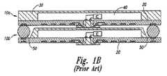
図1Bでは、第一のパッケージ化電子工学装置 10a を、類似した第二の電子工学装置10b に積み重ねるようにして接続したさまを模式的に描いている。第一の電子工学装置 10a の中間基板 20 は、大型ハンダボール 50 を介して、第二の電子工学装置 10b の中間基板(interposer) 20 に接続する。積層型装置 10a-b の欠点のひとつとしては、二枚の中間基板 20 同士の間隔をとるために必要な大型ハンダボール 50 が、中間基板 20 の貴重な空間を費してしまうので、積層型装置 10a-b の占有面積が増えてしまう、ということがある。 FIG. 1B schematically depicts a first packaged electronics device 10a connected in a stacked manner on a similar second electronics device 10b. The
図2は、従来技術にかかる別のパッケージ化マイクロ電子工学装置 60 を模式的に示したものである。装置 60 は、基板 80 に接続した第一のマイクロ電子工学ダイ 70a と、第一のダイ 70a に接続したマイクロ電子工学ダイ 70b とを有している。第一のダイ 70a および第二のダイ 70b は、複数のワイヤボンド配線(wire-bond) 90 を使って基板 80 に電気的に結合している。また、装置 60 は、ダイ 70a および ダイ 70b をカプセル化する外被 95 と、ワイヤボンド配線 90 とをさらに有している。図2に示したパッケージ化マイクロ電子工学装置 60 の欠点のひとつとしては、ダイ 70a および ダイ 70b の一方が、カプセル化後の品質管理試験に落ちてしまうと、良品のダイ 70 を含んでいるのにもかかわらず通常は廃棄されてしまう、ということがある。同様に、ダイ 70a および ダイ 70b の一方が、パッケージ化後に動作不能になったり、かつ/あるいは損傷を受けてしまった場合には、やはりパッケージ化装置の全体 60 を(不良品のダイだけではなく)廃棄することになってしまうのが一般的である。よって、占有面積が少なく且つ良品のダイを有する積層式マイクロ電子工学装置パッケージ化品の供給が要請されている。 FIG. 2 schematically shows another packaged
〔A. 概要〕
以下の開示では、マイクロ電子工学装置、積層式マイクロ電子工学装置、およびそうした装置の製造方法に関する、いくつかの実施形態を述べている。本発明の或る態様が志向しているのは、良品であることが既知な第一のパッケージ化マイクロ電子工学装置、およびその第一の装置に積層式に結合された良品であることが既知な第二のパッケージ化マイクロ電子工学装置、を有する積層式マイクロ電子工学装置部材である。第一の装置には、複数の第一の中間接点を具えた第一の中間基板と、第一の中間接点に搭載され且つ電気的に結合した第一のダイと、を含めることができる。また、第一の装置には第一の外被を含めることもでき、この第一の外被は、第一の中間基板に向いた第一の面と、その第一の面の反対側の第二の面とを有する。こうした場合には、第一の外被が、第一のダイ、および、第一の中間基板の少なくとも一部分をカプセル化するようになっている。また、第一の装置には、第一の外被に少なくとも部分的にカプセル化され且つ対応する第一の中間接点に各々が接した、複数の第一の外被貫通相互接続部、をさらに含めてもよい。第一の相互接続部は、第一の面から第二の面にかけて展延する。[A. Overview]
The following disclosure describes several embodiments relating to microelectronic devices, stacked microelectronic devices, and methods of manufacturing such devices. Certain aspects of the present invention are directed to a first packaged microelectronic device known to be non-defective and a non-defective product coupled to the first device in a stacked fashion. A stacked microelectronic device member having a second packaged microelectronic device. The first apparatus can include a first intermediate substrate having a plurality of first intermediate contacts and a first die mounted on and electrically coupled to the first intermediate contacts. The first device may also include a first envelope, the first envelope being a first surface facing the first intermediate substrate and an opposite side of the first surface. And a second surface. In such a case, the first jacket encapsulates at least a portion of the first die and the first intermediate substrate. The first device further includes a plurality of first jacket through interconnections that are at least partially encapsulated in the first jacket and each in contact with a corresponding first intermediate contact. May be included. The first interconnect extends from the first surface to the second surface.
第二の装置には、複数の第二の中間パッドを具えた第二の中間基板と、第二の中間基板に搭載され且つ電気的に結合した第二のダイと、を含めることができる。また、第二の装置には第二の外被を含めることもでき、この第二の外被は、第二のダイ、および、第二の中間基板の少なくとも一部分をカプセル化するようになっている。対応する第一の相互接続部が第一の外被の第二の面にて露出している部位に、第二の中間パッドが電気的に結合する。 The second apparatus can include a second intermediate substrate having a plurality of second intermediate pads and a second die mounted on and electrically coupled to the second intermediate substrate. The second device may also include a second envelope, the second envelope encapsulating at least a portion of the second die and the second intermediate substrate. Yes. The second intermediate pad is electrically coupled to the portion where the corresponding first interconnect is exposed at the second surface of the first jacket.
第一の相互接続部は、多種多様な構成をとりうる。或る実施形態においては例えば、第一の中間基板の第一の面に接続し且つ第一の外被の周縁部から内向きに第一のダイへと突出した複数のリードフィンガー(lead finger)を、第一の相互接続部が有している。こうしたリードフィンガーは、対応する中間接点に接触し且つ電気的に結合するようにできる。別の実施形態においては、第一の中間接点に接続していてそこから突出しているようなフィラメントを、第一の相互接続部が有する。なおも別の実施形態では、第一の外被を貫いて展延し且つ対応する第一の中間接点とほぼ整列するような、複数の開口部を、第一の相互接続部が有する。個々の開口部は、導電性材料で(少なくとも部分的には)充填される。こうした例として、ハンダ材料を再熔融工程にかけて開口部内に堆積するようにできる。いくつかの実施形態においては、第一の相互接続部が、第一の外被の周縁部に(少なくとも部分的に)沿うので、相互接続部の各々の少なくとも一部分を、第一の外被の周縁部に沿ったところで利用可能となる。しかし他の実施形態においては、第一の相互接続部が、第一の外被の周縁部の基板へ向いた側(inboard)に在るので、周縁部に沿ったと
ころでは第一の相互接続部を利用できない。いくつかの実施形態においては、第二の外被内に(少なくとも部分的には)カプセル化され、且つ、第二の中間基板上の対応する第二の中間接点に接続する、複数の第二の外被貫通相互接続部を、第二の装置がさらに含んでいる。この第二の相互接続部は、上述した第一の相互接続部にだいたい類似した特徴を有していてもよい。なおも別の実施形態においては、良品であることが既知なマイクロ電子工学装置を一個以上、積層式にして、第二の装置に接続し且つ電気的に結合する。The first interconnect can have a wide variety of configurations. In some embodiments, for example, a plurality of lead fingers connected to the first surface of the first intermediate substrate and projecting inwardly from the peripheral edge of the first jacket into the first die. The first interconnect has. Such lead fingers can be in contact with and electrically coupled to corresponding intermediate contacts. In another embodiment, the first interconnect has a filament that connects to and protrudes from the first intermediate contact. In yet another embodiment, the first interconnect has a plurality of openings that extend through the first jacket and are generally aligned with the corresponding first intermediate contact. Individual openings are filled (at least in part) with a conductive material. As an example of this, the solder material can be subjected to a remelting process and deposited in the opening. In some embodiments, the first interconnect is (at least partially) along the peripheral edge of the first jacket so that at least a portion of each of the interconnects is connected to the first jacket. It can be used along the periphery. However, in other embodiments, the first interconnect is on the inboard side of the peripheral edge of the first jacket so that the first interconnect is along the peripheral edge. Department is not available. In some embodiments, a plurality of second encapsulated (at least in part) in a second envelope and connected to a corresponding second intermediate contact on the second intermediate substrate. The second apparatus further includes a jacketed through interconnect. This second interconnect may have features that are generally similar to the first interconnect described above. In yet another embodiment, one or more microelectronic devices known to be good are stacked and connected to and electrically coupled to a second device.
本発明の別の態様では、マイクロ電子工学装置の製造方法を志向する。こうした方法の実施形態のひとつでは、良品であることが既知な第一のマイクロ電子工学装置を、良品であることが既知な第二のマイクロ電子工学装置に近接して配置することを包含している。第一の装置は、第一の中間基板と、その第一の中間基板に電気的に結合した第一のダイと、その中間基板に電気的に結合した複数の導電性相互接続部と、を有してもよい。第一のダイと、第一の中間基板の少なくとも一部分と、第一の相互接続部の少なくとも一部分とを、第一の外被内に包む。第一の相互接続部は、第一の外被の上部において利用可能な端子を有する。本方法はまた、第二の装置を第一の装置に積層式に搭載することも包含している。第二の装置には、第二の中間基板と、その第二の中間基板に電気的に結合した第二のダイとを含めてもよい。第二の外被は、第二のダイと、第二の中間基板の少なくとも一部分とを蔽う。第一の相互接続部の、第一の外被の上部に在る端子が、第二の中間基板の対応する中間パッドに電気的に結合する。 In another aspect of the invention, a method for manufacturing a microelectronic device is directed. One embodiment of such a method involves placing a first microelectronic device known to be good in close proximity to a second microelectronic device known to be good. Yes. The first apparatus includes a first intermediate substrate, a first die electrically coupled to the first intermediate substrate, and a plurality of conductive interconnects electrically coupled to the intermediate substrate. You may have. A first die, at least a portion of the first intermediate substrate, and at least a portion of the first interconnect are encased in a first envelope. The first interconnect has terminals available at the top of the first jacket. The method also includes mounting the second device in a stack on the first device. The second apparatus may include a second intermediate substrate and a second die electrically coupled to the second intermediate substrate. The second jacket covers the second die and at least a portion of the second intermediate substrate. A terminal of the first interconnect at the top of the first jacket is electrically coupled to a corresponding intermediate pad of the second intermediate substrate.
本明細書を通じ、「部材」("assembly")および「副部材」("subassembly")という用語は、製品の中のさまざまな物品のことを含む。そうした物品の例としては、活性部品を有する半導体ウェハ、独立した集積回路ダイ、パッケージ化ダイ、ならびに、二個以上の微小特徴的構造を持つ半製品もしくは部品を含んだ装置(パッケージ化積層式ダイなど)、がある。本発明の或る実施形態に特有の多数の特徴を、これらの実施形態群を徹底的に理解できるようにするため、以下の記載と図3Aから図20に示してある。しかし当業者は、そうした特徴のうちのいくつかを使わずに本発明を実施することもできるし、あるいは、本発明に特徴を追加して実施することもまた可能なのである。本発明の実施形態の記載を不必要に邪魔せぬよう、公知の構造および機能については特に詳しく述べてはいない。 Throughout this specification, the terms “component” and “subassembly” include various articles in a product. Examples of such articles include semiconductor wafers with active components, independent integrated circuit dies, packaging dies, and devices containing semi-finished products or parts with two or more micro-characteristic structures (packaged stacked die). and so on. Numerous features specific to certain embodiments of the present invention are set forth in the following description and in FIGS. 3A-20 in order to provide a thorough understanding of these embodiments. However, one of ordinary skill in the art can implement the invention without using some of these features, or can add features to the invention. In other instances, well-known structures and functions have not been described in detail so as not to unnecessarily obscure the description of the embodiments of the invention.
〔B. 積層式マイクロ電子工学装置の製造方法およびそうした方法を用いてつくられたマイクロ電子工学装置に関する実施形態群〕
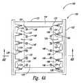
図3Aから図7には、本発明の或る実施形態にかかる、複数のマイクロ電子工学装置を積層型にしたものを製造する方法の工程段階を描いている。より具体的に述べると、図3Aは、本方法の初期段階における副部材 100 の平面図であり、部分的に模式的に描いてある。また図3Bは、図3Aの線 3B-3B にほぼ沿って得られる、側方からの断面図である。図3Aと図3Bをともに参照すると、副部材 100 には、支持部品 102 (中間基板、プリント回路基板、もしくは別の適切な構造体など)と、この支持部品上のリードフレーム 120 とが含まれる。示した実施形態では、支持部品 102 が、 (a) 複数の接点 108 を有する、第一の側 104 と、 (b) 第一の側 104 の反対側であり且つ複数のパッド 110 を有する、第二の側 106 と、 (c) 接点 108 と、支持部品 102 の第二の側 106 に在る対応するパッド 110 (もしくは不図示である他の接点)との間の、複数の導線 112 (もしくは他の種類の導電線)とを含んでいる。複数の接点 108 をアレイ状に配置して、リードフレーム 120 上の対応する接点、および/もしくは支持部品 102 に接続した一個以上のマイクロ電子工学ダイと、電気的に接続するようにできる(詳しくは後述)。この実施形態の或る態様では、支持部品 102 の第二の側 106 に在るパッド 110 を、標準的なJEDEC pinoutに則ったアレイとして配置する。他の実施形態群では、支持部品 102 に、第一の端部 104 および/もしくは第二の端部 106 に在る接点/パッドの多種多様な配置を含めてもよい。[B. Manufacturing Group of Stacked Microelectronic Device and Embodiments Related to Microelectronic Device Made Using Such Method]
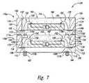
FIGS. 3A-7 illustrate process steps of a method of manufacturing a stack of microelectronic devices according to an embodiment of the present invention. More specifically, FIG. 3A is a plan view of the
リードフレーム 120 は、自己支持式構造をとっており、一般的には、周縁壁 122 および複数のリードフィンガー 124 を有する。リードフィンガー 124 同士には、間隙 126 をとってある。周縁壁 122 の内表面と、各リードフィンガー124 とが併さって、リードフレーム 120 中の開口部 129 の内縁部 128 をかたちづくっている。この実施例では、開口部 129 が、リードフレーム 120 の全厚さを貫通している。リードフレーム 120 は金属でつくってもよいし、もしくは別の適切な導電性材料でつくってもよい。いくつかの実施形態においては、リードフレーム 120 として、貴金属(金、銀、もしくはパラジウムなど)で鍍金した導電性材料を使ってもよい。あるいは、リードフレーム 120 として、導電性材料で覆った非導電性材料を使ってもよい。各リードフィンガー 124 の一部分が、支持部品 102 上の対応する接点 108 と接続している。 The
図示した実施形態では六個のリードフィンガー 124 を描いてはいるが、リードフレーム120 に電気的に結合することになるマイクロ電子工学ダイの構成に(少なくとも部分的に)応じて、リードフレーム 120 が別の数のリードフィンガー 124 を持つようにしてもよい。図示した実施形態ではリードフィンガー 124 がすっきりとした単純な四角形になっているが、なおも別の実施形態ではその代わりとして、もっと複雑な形状を有するリードフィンガー 124 を用いてもよい。 Although the illustrated embodiment depicts six
この実施形態の或る態様では、周縁壁 122 および各リードフィンガー 124 の高さがほぼ等しく D1 である。詳しくは後述するが、高さ D1 は、支持部品 102 上に配置することになるマイクロ電子工学ダイの高さよりも、大きくしておくべきである。しかしながら他の実施形態においては、リードフィンガー 124 の高さが、周縁壁 122 の高さと異なっていてもよい。In one aspect of this embodiment, the
次に図4Aおよび図4Bに移ると、ここではマイクロ電子工学ダイ 140 を、リードフレーム 120 の開口部 129 の内部に配置可能である。なおここでは、単独のリードフレーム 120 および単独のダイ 140 が支持部品 102 に接続しているさまを示してはあるが、複数のリードフレーム 120 および複数のダイ 140 を支持部品 102 に接続して、複数のマイクロ電子工学装置を製造することも可能である。ダイ 140 には、表面(活性面)部 142 と、活性面部 142 の反対側に在る背面部 144 と、集積回路 146 (模式的に示した)と、を含めることができる。ダイ 140 の背面部 144 が、開口部 129 内部の支持部品 102 の露出した第一の側 104 に接続している。また、活性面部 142 にアレイとして配置され、且つ、集積回路 146 に電気的に結合した、複数の端子 148 (接合パッドなど)を、ダイ 140 が有してもよい。すると、電源電圧、ground電圧、および信号を、ダイ 140 中の集積回路 146 へと与えるための外部接点が、端子 148 により得られることになる。示した実施形態においては、端子 148 が、ダイ 140 の周縁部に隣接し、且つ、支持部品 102 上の対応する接点 108 にワイヤボンド配線 150 (または他の種類の接続子)を介して電気的に結合している。一般的にワイヤボンド配線 150 のループ高さは、リードフレーム120 の高さ D1 よりも低くして、封止材(encapsulant)でワイヤボンド配線 150 を完全にカプセル化できるようにしておく(詳しくは後述する)。Turning now to FIGS. 4A and 4B, a
他の実施形態においては、ダイ140 が他の特徴的構造を有してもよく、且つ/あるいは、ダイ 140 を、支持部品 102に他の配置法を以って電気的に結合してもよい。そうした他の配置法としては、flip-chip構成法(FCIP)、もしくは別の適切な手法を使用可能である。さらには、リードフレーム 120 とダイ 140 を支持部品 102 に接続する順番を変更してもよい。上述した実施形態では、ダイ 140 を支持部品 102 に接続する前に、リードフレーム 120 を支持部品 102 に接続する。だが他の実施形態では、リードフレーム 120 を支持部品 102 に接続する前に、ダイ 140 を支持部品 102 に接続する。なおも別の実施形態においては、リードフレーム 120 とダイ 140 を、支持部品 102 に同時に接続できる。 In other embodiments, the
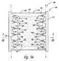
次に図5Aと図5Bを見ると、ここでは、ダイ 140 を接点 108 に電気的に結合した後に開口部 129 内に封止材 160 を入れることで、副部材 100 の少なくとも一部分をカプセル化する外被 162 をつくりだせる。より具体的には、支持部品 102 の露出した第一の側 104 と、リードフレーム 120 の内縁部 128 と、ダイ 140 とで、開口部 129 の内部に窩部 152 を劃定する。この窩部 152 を封止材 160 で(部分的にかもしくは完全に)充填することで、外被 162 ができる。示した実施形態では、窩部 152 は封止材 160 で完全に満たされており、外被 162 の上部 164 は、リードフィンガー 124 の上部 130 とほぼ同一平面をなしている。だが他の実施形態においては、ダイ 140 と対応するワイヤボンド配線 150 が完全にカプセル化される程度を保ちつつ、外被 162 の上部 164 を、リードフィンガー 124 の上部 130 よりも低くできる。 Turning now to FIGS. 5A and 5B, the
封止材 160 は、適切な塗布工程を介して開口部 129 内に堆積できる。そうした塗布工程としては例えば、旧来の注入成形法、成膜法、もしくは他の適切な工程、がある。いくつかの実施形態においては、封止材 160 を窩部 152 に入れてただ充填し、ダイ 140 とワイヤボンド配線 150 を覆うようにできる。封止材 160 がリードフィンガー 124 の上部 130 を越えて外へ流れ出した場合には、封止材の盛り上がったところを、切削、研磨、もしくは他の適切な手法を用いて除去できる。だが他の実施形態においては、封止材 160 の流れは、成形用部品(不図示)を使って抑制できる。こうした成形用部品には、リードフィンガー 124 の上部 130 と実質的にくっつくようになっているほぼ平坦な成形面が具わり、封止材 160 がリードフレーム 120 を越えて流れださないようになっている。 The
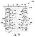
図5Aからよくわかると思うが、周縁壁 122 は、各リードフィンガー 124 と互いに物理的に接続しており、上述したように封止材 160 を受ける窩部 152 を劃定する助けになっている。しかし、外被 162 を適切につくれたならば、周縁壁122 はもう不要である。ゆえに、副部材 100 を線 A-A に沿って切断して周縁壁 122 を取り外し、パッケージ化マイクロ電子工学装置 170 (図6Aおよび図6B)を形成して、装置 170 の周縁部近傍に間隔をとって複数のリードフィンガー 124 が配置されるようにできる。副部材100 の切断には、従来のウェハ鋸、高圧水ジェット、レーザー、などを使用できる。他の実施形態においては、線 A-A を、ダイ 140 のほうへと若干内側にずらして、各リードフィンガー 124 の一部分も周縁部 122 といっしょに取り除くようにしてもよい。 As can be seen in FIG. 5A, the
さて次に図6Aおよび図6Bを見ると、ここでは装置 170 をパッケージ化後に試験にかけ、装置が完全に機能するかどうかを確認して、良品であるのがわかっている装置だけを以降の工程にかけるようにできる。また、複数の電気結合子 166 (ハンダボールなど)を、支持部品 102 の第二の側 106 に在る対応するパッド 110 に接続できる。一般的には、電気結合子 166 が良品であることが既知な装置 170 だけに接続していることを確かめた後に、電気結合子166 を装置 170 に接続する。しかしいくつかの実施形態では、試験前に電気結合子を装置に接続してもかまわない。 Turning now to FIGS. 6A and 6B, now the
装置 170 の特徴のひとつとして、外被 162 の上部 164 が、リードフィンガー 124 の上部 130 とほぼ共平面関係になる、ということがある。すると、装置 170 は力学的に安定な構造となり、また各リードフィンガー 124 が、支持部品 102 の第二の側 106 に在るパッド 110 と、対応するリードフィンガー 124 の上部 130 との間を結ぶ導電路を画定する。後述するように、この特徴によって二個以上の装置 170 の積み重ねがやりやすくなる。装置170 の別の特徴として、各リードフィンガー 124 の少なくとも一部が、外被 162 の周縁部に沿ったところで利用可能となる、ということもある。もっと具体的に云うと、各リードフィンガー 124 が、ダイ 140 に向いた表面 132 と、その表面 132 の反対側であり且つ外被 162 の周縁部にほぼ沿った背面 134 と、を有するということであ
る。この特徴の効果のひとつは、各リードフィンガー 124 の利用可能な背面 134 によって、さらなる接点が得られるので、装置 170 の試験が容易になる、というものである。One feature of the
図7は、積層式マイクロ電子工学装置部材 190 の側方からの断面図であり、部材190 は、下部マイクロ電子工学装置 170b と、その下部装置 170b の上面に積み重ねられた上部マイクロ電子工学装置 170a と、を有している。上部装置 170a および下部装置 170b は、図6Aおよび図6Bにからめて上述したマイクロ電子工学装置 170 とだいたい類似している。だが、上部装置 170a では、支持部品 102 の第二の側 106 に在るパッド 111a のアレイの配置が、装置 170 のパッド 110 のアレイの配置とは異なっているという点で、上部装置 170a と上述の装置 170 とには違いがある。より具体的に云うと、装置 170a が、積層式部材中の「上側の」装置となるように構成されているので、パッド 111a が、下部装置 170b の対応するリードフィンガー 124 と接続するように配置される。こうして、上部装置 170a と下部装置 170b とが電気的に結合されるのである。さらには、上部装置 170a は一般に、パッド 111a に接続した電気結合子を有していない。他の実施形態においては、上部装置 170a および/もしくは下部装置 170b の配置が異なっていてもよい。例えば、上述した装置 170 のパッド 110 の配置とだいたい類似した配置をされた複数のパッド 110 a (破線で示してある)を、上部装置 170a が有してもよい。また、下部装置 170b のリードフィンガー 124 は、各リードフィンガー 124 の表面 132 から突出した結合部位 124a (破線で示してある)を有してもよく、この結合部位 124a は対応するパッド 110a に接続するように構成されている。なおも他の実施形態においては、上部装置 170a および下部装置 170b が、他の特徴的構造を含んでいてもよい。 FIG. 7 is a cross-sectional view from the side of a stacked
上部装置 170a を下部装置 170b に結合するにあたっては、上部装置 170a のパッド 111a を、下部装置 170b の対応するリードフィンガー 124 に接続して電気的に結合する。示した実施形態では、上部装置の支持部品 102 の第二の側 106 が、下部装置の外被 162 の上部 164 と直接に接している。つまり、積層式部材 190 は、上部装置 170a と下部装置 170b の間に充填材料を有していない。しかしながら前述したように、他の実施形態においては、外被 162 の上部 164 が、リードフィンガー 124 の上部 130 と共平面関係になくともよい。つまり、上部装置 170a と下部装置 170b の間の間隙(窩部)内に、充填材料(不図示)を堆積できるということである。こうした充填材料(エポキシ樹脂、もしくは他の適切な成形材料など)によって、積層式部材 190 の剛直性が高まり、さらには、湿気、化学物質、および他の夾雑物から、上部装置 170a と下部装置 170b の部品群を保護できる。とは云え、この充填材料は任意付加部品である。 In coupling the upper device 170a to the
図3Aから図7にからめて上述した方法を使って作成した装置 170 の利点のひとつとして、この装置は互いに積み重ねることができる、ということがある。マイクロ電子工学装置を積み重ねることで、所与の表面積(占有面積)内で、容量および/もしくは性能を増大できる。例えば、上部マイクロ電子工学装置 170a を、下部マイクロ電子工学装置170b の上面に載せて積んで、下部装置 170b を回路基板もしくは他の外部装置に接続すると、上部装置 170a が、余分の表面積を回路基板上に占めることなく、回路基板もしくは他の外部装置と電気的且つ機能的に結合できる。 One advantage of the
積層式部材 190 の特徴のひとつとして、上部装置 170a と下部装置 170b の双方を、パッケージ化後且つ積載前に試験にかけることで、これらの装置を組み上げる前にその機能が適正にはたらいていることを確認できる、ということがある。こうすると、欠陥のある装置を検出して、前述した方法を使って作成する積層式部材 190 からそうした欠陥のある装置を除くことができるので、積層式部材 190 の各々が一般に、良品であることが既知な装置のみを含むことになる。ゆえに、積層式部材 190 の処理能力を向上できるのである。そして、上述したパッケージ化工程の歩留りを改善し、機能不全であるおよび/もしくは欠陥のある装置の個数を低減できる。 One of the features of the stacked
図3Aから図7にからめて上述した方法を使って作成した装置 170 の別の特徴として、電気結合子166 が、リードフィンガー 124 の基板寄り側に位置する、ということがある。この特徴の利点は、積層式部材 190 の占有面積を、旧来の積層式装置(図1Bに示した、ハンダボール 50 がダイ 40 の基板から離れた側に在る、装置 10a, 10b など)に較べて少なくできる、ということである。携帯電話、PDA、および他の電気製品といった、使用するマイクロ電子工学部品の大きさを縮めることに始終汲々としているような装置においては、マイクロ電子工学装置の占有面積を最小化することが特に重要である。 Another feature of the
〔C. 積層式マイクロ電子工学装置の製造方法およびそうした方法を用いてつくられたマイクロ電子工学装置に関する付加的な実施形態群〕
図8から図21には、積層式マイクロ電子工学装置の製造方法にかかる他の実施形態における種々の工程段階を示してある。以降に述べる方法およびその方法を用いてつくる装置では、図3Aから図7にからめて述べた装置 170 および積層式部材 190 と同様の、多数の効果が得られる。[C. Additional Embodiments Concerning Manufacturing Method of Laminated Microelectronic Device and Microelectronic Device Made Using Such Method]
8 to 21 show various process steps in another embodiment of a method for manufacturing a stacked microelectronic device. In the method described below and the apparatus made using the method, a number of effects similar to those of the
例えば図8は、支持部品 202 上にアレイとして配置された複数のマイクロ電子工学ダイ 220 (図では三個のみ示した)を有する副部材 200 の、側方からの模式的な断面図である。中間基板、プリント回路基板、もしくは、ダイ 220 を担持するための適切な他の支持部品を、支持部品 202 が有していてもよい。示した実施形態においては、支持部品 202 が、 (a) 複数の接点 208 を有する第一の側 204 と、 (b) 複数の第一のパッド 210
および複数の第二のパッド 212 を有する第二の側 206 と、を含んでいる。接点 208 をアレイ状に配置して、ダイ 220 上の対応する端子に電気的に接続できる。また、複数の第一のパッド 210 および複数の第二のパッド 212 もアレイ状に配置して、複数の電気結合子(ハンダボールなど)および/もしくは他の種類の電気的相互接続部を受けるようにできる。支持部品 202 はさらに、複数の導電線 214 も含み、この導電線 214 が、接点 208 を、対応する第一のパッド 210 および第二のパッド 212 に電気的に結合する。本実施形態の態様のひとつでは、支持部品 202 の第二の側 206 に在る複数の第一のパッド 210 および複数の第二のパッド 212 を、標準的なJEDEC pinoutに則ったアレイとして配置する。他の実施形態群では、支持部品 202 に、第二の側 204 および/もしくは第二の側 206 に在る接点/パッドの多種多様な配置を含めてもよい。For example, FIG. 8 is a schematic cross-sectional view from the side of a
And a
個々のダイ 220 は、集積回路 222 (模式的に示した)と、表(活性)側 224 と、活性側 224 においてアレイ状に配置され且つ集積回路 222 に電気的に結合した複数の端子
226 (接合パッドなど)と、活性側 224 の反対側である背部側 228 と、を有する。ダイ 220 の背部側 228 は、支持部品 202 に、接着剤 230 (接着フィルム、エポキシ、テープ、糊、もしくは他の適切な材料など)を用いて接着する。複数のワイヤボンド配線 232 もしくは他の種類の接続子によって、ダイ 220 上の端子 226 を、支持部品 202 上の対応する接点 208 に結合する。なお図示したダイ群220 は同じ構造をしているのだが、他の実施形態では、ダイ群 220 が、異なる特徴を有し異なる機能を発揮するようになっていてもかまわない。さらなる実施形態においては、ダイ群 220 を支持部品 202 に接続し電気的に結合するに際して、FCIP configurationや別の適切な手法などの他の配置法を用いてもいい。Each die 220 includes an integrated circuit 222 (shown schematically), a front (active)
226 (such as a bonding pad) and a
図9は、複数の相互接続部もしくはフィラメント 234 を、支持部品 202 の第一の側 204 に在る接点 208 に接続した後の、副部材 200 の側方からの模式的な断面図である。相互接続部もしくはフィラメント 234 としては、対応する接点 208 に接続し電気的に結合した薄型・可撓性のワイヤが含まれうる。示した実施形態においては例えば、相互接続部 234 として、接点 208 に接続し接点 208 から離れるように支持部品 202 の第一の側
204 のほぼ法線方向に突出した、比較的直線的である自立式ワイヤボンド配線が含まれ
る。相互接続部234 の高さ H は、支持部品 202 の第一の側 204 を基準とし、得られるパッケージ化装置の所望の高さに(少なくとも部分的には)依拠している。また、各相互接続部 234 の末端には、電気結合子 236 (球状部位など)があってもよい。詳しくは後述するが、電気結合子 236 によって、ダイ 220 上に積載可能な一個以上の装置との相互接続の接合がやりやすくなる。相互接続部 234 は、ワイヤボンド配線 232 をつくった後に、接点 208 へと接続するのが一般的である。だが、いくつかの実施形態群では、相互接続部 234 とワイヤボンド配線 232 を同時につくってもよい。図15にからめて後述する実施形態などの他の実施形態群においては、相互接続部 234 が、多様な配置および/もしくは多様な特徴を有していてもよい。FIG. 9 is a schematic cross-sectional view from the side of the
Included are 204 freestanding wire bond lines that protrude in a generally normal direction and are relatively straight. The height H of the
図10では、封止材 240 を支持部品 202 の上に堆積することで、ダイ 220 、ワイヤボンド配線 232 、および相互接続部 234 の少なくとも一部分、をカプセル化する複数の外被 242 をつくっている。こうした封止材240 を支持部品 202 上に堆積するにあたっては、適切な塗布工程(従来の注入成形法、成膜法、もしくは他の適切な工程など)を使用できる。 In FIG. 10, the
次に図11を見ると、ここでは外被 242 の最上部 244 (破線で示している)を除去することで、相互接続部 234 の末端に在る電気結合子 236 を(少なくとも部分的に)露出させている。外被 242 の最上部 244 の除去に際しては、レーザー研磨工程もしくは他の適切な工程を使用できる。他の実施形態群においては、副部材 200 のカプセル化中に使う鋳型が、電気結合子 236 の配置に対応した窩部もしくは凹部を含んでいる。つまり、外被 242 の形成時には、個々の電気結合子 236 がカプセル化されないことになり、したがって研磨工程もしくは除去工程は不要である。なおも別の実施形態群では、封止材 240
を別の適切な工程を用いて堆積し、装置を鋳型から取り外した後にも電気結合子 236 が露出したままになるようにする。なおも他の実施形態群においては、カプセル化の後にレーザー掘削工程を使って、相互接続部 234 の少なくとも一部分を分離・露出させてから、得られたビア穴内に導電性材料(金など)を堆積して、複数の導電性パッドを、外被 242 の最上部 244 に、所望の配置でつくることができる。所望であれば、その後に分配構造体を最上部 244 につくって、導電性パッドからの信号を、接点のより大型のアレイへと分配するようにしてもよい。相互接続部 234 の電気結合子 236 を少なくとも部分的に露出させた後に、副部材 200 を線 B-B に沿って切断して、複数の独立したマイクロ電子工学装置 250 を単一化できる。Turning now to FIG. 11, the
Is deposited using another suitable process so that the
次に図12を見ると、ここでは個々の装置 250 は 試験済のパッケージ化後のものであって、各装置が適正に機能していることを確認してある。なので、良品であることが既知な装置だけがさらなる工程にかけられる。さらには、複数の電気結合子 252 (ハンダボールなど)を、支持部品 202 の第二の側 206 に在る対応するパッド 212 に接続できる。これらの電気結合子 252 は、良品であることが既知な装置にのみ接続していることを試験してから、装置 250 へと接続するのが一般的である。だが、いくつかの実施形態群では、電気結合子を試験する前に装置に接続してもよい。 Turning now to FIG. 12, here each
いくつかの実施形態群においては、一個以上の独立した装置 250 を逐次積み重ねて、積層式マイクロ電子工学装置部材を作成できる。図13には一例として、積層式マイクロ電子工学装置部材 290 の側方からの断面図を示した。この部材 290 は、下部マイクロ電子工学装置 250b の上面に載せて積んだ上部マイクロ電子工学装置250a を含んでいる。上部装置 250a および下部装置 250b は、図8から図12にからめて上述した装置 250 とだいたい類似している。上部装置 250a を下部装置 250b に結合するにあたっては、上部装置の支持部品 202 の第二の側 206 を、下部装置の外被 242 の最上部 244 に、接着剤 260 を用いて接着できる。こうした接着剤 260 としては、接着フィルム、エポキシ、テープ、糊、もしくは他の適切な材料などを使用できる。下部装置の電気結合子 236b を、上部装置 250a 上の対応する第一のパッド 210a に、電気的に結合できる。示した実施形態においては例えば、各電気結合子 236b が、対応する第一のパッド 210a に、電気接続子 262 を介して結合している。この電気接続子 262 はまた、上部装置 250a を下部装置 250b に(少なくとも部分的に)物理的に結合するものであってもよい。電気接続子 262 としては、当該技術分野で公知のように再熔融したハンダ接続、もしくは他の適切な接続子、が含まれうる。 In some embodiments, one or more
いくつかの実施形態群では、充填材料 264 を、上部装置 250a と下部装置 250b の間の領域内に堆積可能である。そして、上部装置 250a の上にこれ以上装置を積まないのであれば、上部装置 250a の最上部 244 に在る露出した電気結合子 236a を覆うように、充填材料 264 を堆積できる。充填材料 264 によって、積層式部材 290 の剛直性が高まり、さらには、湿気、化学物質、および他の夾雑物から、上部装置 250a と下部装置 250b の部品群を保護できる。或る実施形態においては、充填材料 264 として、エポキシ樹脂などの成形材料が含まれうる。他の実施形態においては、充填材料 264 として、他の適切な材料が含まれうる。充填材料 264 の堆積は、任意付加工程であって、これが含まれない実施形態があってもよい。 In some embodiments, the
他の実施形態群においては、付加的なマイクロ電子工学装置を、上部マイクロ電子工学装置 250a の上に積み重ねてもよい。こうしたことを行うにあたっては、上部装置 250a の最上部 244 に在る電気結合子 236a を露出させてから、一個以上の付加的な装置(不図示)を、上部装置 250a に載せて電気結合子 236a に電気的に結合する。なおも別の実施形態では、上部装置 250a と下部装置 250b が違う装置であってもよい。例えば、上部装置 250a のマイクロ電子工学ダイ 220 と、下部装置 250b のマイクロ電子工学ダイ 220 は、同じ種類のダイであってもよいしもしくは違う種類のダイであってもよく、ならびに/あるいは、上部装置 250a と下部装置 250b が他の特徴的構造を有してもよい。 In other embodiments, additional microelectronic devices may be stacked on top of the microelectronic device 250a. In doing so, the electrical coupler 236a at the top 244 of the upper device 250a is exposed, and then one or more additional devices (not shown) are placed on the upper device 250a and placed on the electrical coupler 236a. Is electrically coupled. In still another embodiment, the upper device 250a and the lower device 250b may be different devices. For example, the microelectronic die 220 of the upper device 250a and the microelectronic die 220 of the lower device 250b may be of the same type or different types and / or Device 250a and lower device 250b may have other characteristic structures.
図14には、本発明の別の実施形態に応じて構築した、マイクロ電子工学装置 350 を示してある。このマイクロ電子工学装置 350 は、図8から図12にからめて上述したマイクロ電子工学装置 250 とほぼ同様である。つまり、図8から図12と図14とでは、類似の参照番号は類似の要素を指している。装置 350 が装置 250 と異なっているところは、装置 350 の相互接続部 334 の構成が、装置 250 の相互接続部 234 のそれとは違うことである。より具体的には、装置 350 の相互接続部 334 がワイヤループを含むことで、このワイヤループの球状部位とかがり部位のどちらもが、支持部品 202 の対応する接点 208 に在るようにできる。こうしたループ状相互接続部の高さ H を、上述した相互接続部 234 のそれとほぼ同様にすることで、相互接続部 334 の最上部 335 を、外被 242 の最上部 244 にて露出させることができる。こうしたループ状相互接続部 334 の利点のひとつとして、このような相互接続部は一般に、前述した単一フィラメント式相互接続部 234 よりも耐久性が高いことが期待できる、ということがある。なぜなら、こういったループ状相互接続部は、対応する接点 208 により堅固に繋留されることになるため、成形工程中に曲ってしまったり接点から外れてしまったりしづらいからである。さらには、いくつかの実施形態群では、ループ状相互接続部 334 のインダクタンスを、相互接続部234 のそれよりも小さくできる。 FIG. 14 shows a
図15Aから図18には、複数の積層式マイクロ電子工学装置を製造する方法のなおも別の実施形態における工程段階を示した。図15Aは、一例としての、本方法の初期段階における副部材 400 の、部分的に模式的な等角図である。副部材 400 は、複数のマイクロ電子工学ダイ 430 (破線で示した)を含んでおり、これらのダイ群 430 は、支持部品 402 上にアレイとして配置され、外被 462 でカプセル化されている。なお、示した実施形態では、支持部品 402 に接続しているダイ 430 は四つだけではあるが、支持部品 402 に接続するダイ 430 の数を変えて、複数のマイクロ電子工学装置をつくってもよい、と
いうことは理解できるであろう。副部材 400 は、外被 462 を貫いて支持部品 402 の第一の側 404 へと至るように展延する、複数の小型の開口部もしくはビア穴 440 ("針穴")をさらに含む。開口部群 440 は概して、個々のダイ 430 同士の間の"路"(非活性領域)に配置される。開口部 440 については、図16Aおよび図16Bにからめて詳しく後述する。15A-18 show process steps in yet another embodiment of a method of manufacturing a plurality of stacked microelectronic devices. FIG. 15A is a partially schematic isometric view of the
図15Bは、図15Aの線 15B-15B にだいたい沿った、側方からの断面図である。図15Aと図15Bに関してはともに、支持部品 402 として、中間基板、プリント回路基板、もしくは他の適切な支持部品、を使ってよい。示した実施形態においては、支持部品 402 が、 (a) 複数の第一の接点 408 および複数の第二の接点 409 を有する、第一の側 404 と、 (b) 第一の側 404 の反対側であり且つ複数の第一のパッド 410 および複数の第二のパッド 411 を有する、第二の側 406 と、 (c) 第一の接点 408 および/もしくは第二の接点409 と、支持部品 402 の第二の側 406 に在る対応する第一のパッド 410 および/もしくは第二のパッド 411 または他の接点(不図示)との間に在る、複数の導電線 412 もしくは他の種類の導電線と、を含む。第一の接点 408 および第二の接点 409 をアレイ状に配置して、ダイ 430 およびそのパッケージ化ダイに積載した一個以上の装置の上の対応する接点に、電気的に接続できる。この実施形態の態様のひとつでは、支持部品 402 の第二の側 406 に在る第二のパッド 411 を、標準JEDEC pinoutに応じたアレイ状に配置する。他の実施形態においては、支持部品 402 の含む接点ならびに/またはパッドの、数もしくは配置を変えてもよい。 FIG. 15B is a cross-sectional view from the side, generally along
個々のマイクロ電子工学ダイ430 には、表面側(活性側) 432 と、活性側 432 の反対側である背面側 434 と、集積回路 436 (模式的に示してある)とを含められる。ダイ 430 の背面側 434 を、支持部品 402 の第一の側 404 に、接着剤(不図示)で接着できる。また、ダイ 430 には、活性側 432 にてアレイをなすように配置され且つ集積回路 436 に電気的に結合された、複数の端子 438 (接合パッドなど)を含めてもよい。示した実施形態においては、複数の端子 438 をダイ 430 の周縁部に隣接して配置することで、ダイ 430 を支持部品 402 にchip-on-board(COB)構成を以って電気的に結合するために使用できる。より具体的には、複数のワイヤボンド 439 もしくは他の種類の接続子が、端子 438 と、支持部品 402 上の対応する第二の接点 409 との間に展延する。他の実施形態においては、ダイ 430 が他の特徴的構造を有してもよく、かつ/あるいは、他の配置法を以ってダイ 430 を支持部品 402 に接続して電気的に結合してもよい。そうした他の配置法としては例えば、FCIP構成、board-on-chip(BOC)構成、もしくは別の適切な構成がある。 Each microelectronic die 430 can include a front side (active side) 432, a
次に図16Aと図16Bを見ると、ここでは導電性材料 442 を各開口部 440 内に堆積して、外被 462 を貫いて支持部品 402 上の対応する第一の接点 408 へと至るよう展延している、複数の導電性相互接続部 444 をつくっている。或る実施形態においては例えば、ハンダボール(不図示)を各開口部 440 の最上部に配置してから再熔融させ、ハンダが対応する開口部をほぼ満たすようにする。とはいえ他の実施形態では、導電性材料 442 を他の適切な手法で開口部 440 内に堆積できる。導電性相互接続部 444 を形成した後には、副部材 400 を線 C-C に沿って切断して、複数の独立したマイクロ電子工学装置
450 を単一化できる。Turning now to FIGS. 16A and 16B, a
450 can be unified.
図17Aでは一例として、単一化した装置 450 の、部分的に模式化した等角図を示してある。また、図17Bは、図17Aの線 17B-17B にほぼ沿った、側方からの断面図である。図17Aおよび図17Bを併せて参照すると、本方法のこの工程段階で個々の装置
450 を試験し、各装置が適切に機能しているかを確認して、良品であることがわかった装置のみを後続の工程にかけるようにできる。図17Aおよび図17Bに示した装置 450
を、積層式マイクロ電子工学装置中の「底部」もしくは「下部」の装置として構築して
、複数の電気結合子(不図示)が、支持部品 402 の第二の側に在る対応する第二のパッド 411 に接続するようにできる。前述したように、第二のパッド 411 は、標準JEDEC pinoutになるよう配置する。一方、装置 450 は「上部の装置(つまり、一個以上の下部装置に載せた装置)になるように構築されており、第二のパッド 411 を異なる配置にしておいてもよいし、かつ/あるいは、電気結合子を第二のパッドに接続しないようにしてもいい。In FIG. 17A, as an example, a partially schematic isometric view of the
450 can be tested to ensure that each device is functioning properly, so that only those devices that are found to be good are subjected to subsequent steps. The
Is constructed as a “bottom” or “bottom” device in a stacked microelectronic device, with a plurality of electrical couplers (not shown) corresponding to the second side of the
装置 450 の特徴のひとつとして、装置 450 の最上部 454 および周縁部 452 にて、相互接続部 444 が少なくとも部分的に露出する、ということがある。するとこの露出した相互接続部 444 によって、支持部品 402 の第二の側 406 に在る第一のパッド 410 および第二のパッド 411 と、装置 450 の最上部 454 との間に、導電路が劃定されることになるわけである。後述するが、こうした特徴により、二個以上の装置 450 の積み重ねがやりやすくなる。 One feature of the
図18では一例として、積層式マイクロ電子工学装置部材 490 の部分的に模式化した等角図を示してある。この部材 490 には、第一のマイクロ電子工学装置 450a と、第一のマイクロ電子工学装置 450a 上に積まれた第二の上部マイクロ電子工学装置 450b と、第二の上部マイクロ電子工学装置 450b 上に積まれた第三のマイクロ電子工学装置 450c と、が含まれている。これらの装置 450a-c は、図15Aから図17Bにからめて上述した装置 450 とだいたい同様のものである。第二の装置 450b を第一の装置 450a に結合するにあたっては、第二の装置の支持部品 402 の第二の側 406 に在る第一のパッド 410b を、第一の装置 450a の最上部 454 に在る第一の装置の相互接続部 444 の露出した部位に接続することで行える。第三の装置 450c の第二の装置 450b への結合もだいたい同様にできる。 In FIG. 18, as an example, a partially schematic isometric view of a stacked
或る実施形態においては、装置を積み重ねる前に、複数の超小型の調整穴(不図示)を、各装置 450a-c を完全に貫通するように形成する。装置群 450 をまとめて積み重ねた最中か積み重ねた後かに、積層式部材 490 の調整穴に、レーザー光線もしくは他の適切な光線を直接通すことで、個々の装置が互いに対して適正に並んでいて、各装置上の外部電気接点が、隣の装置(群)に適切な接点を介して接続しているかどうかを確認できる。例えば、光線が積層式部材を完全に通過できたなら、各装置の調整穴は適正に並んでいることになる。一方、光が積層式部材を完全に通過できなかったら、装置のうちの一個以上が整列できていないことになる。他の実施形態においては、他の適切な手法を使って、積層式部材 490 の個々の装置 450 を互いに対して整列させられる。 In some embodiments, prior to stacking the devices, a plurality of ultra-small adjustment holes (not shown) are formed to completely penetrate each device 450a-c. The individual devices are properly aligned with each other by passing a laser beam or other suitable beam directly through the adjustment holes in the
図19および図20には、本発明のなおも別の実施形態に応じて、複数の積層式マイクロ電子工学装置を製造する方法の工程段階を示してある。この方法には、図15Aから図17Bにからめて上述した工程とだいたい同じ工程段階を含めてもよい。図19には一例として、マイクロ電子工学装置 550 の、側方からの断面図を示してある。この装置 550 には、図15Aから図17Bにからめて上述した装置 450 とほぼ似かよった多数の特徴がある。しかし装置 550 のダイの配置と相互接続部の構成は、装置 450 のダイ 430 の配置と相互接続部 444 の構成とは異なっている。より具体的には、装置 550 がFCIP構成を有するダイ 530 を有しているところが、上述した装置 450 のダイ 430 のCOB構成と違う。さらに云えば、装置 550 が持つ複数の相互接続部 544 は、装置 550 の周縁部 554 の基板へ向いた側に位置しており、相互接続部 444 が装置 450 の周縁部 452 近辺で少なくとも部分的に露出していたのとは異なっている。 19 and 20 illustrate the process steps of a method of manufacturing a plurality of stacked microelectronic devices in accordance with yet another embodiment of the present invention. This method may include substantially the same process steps as described above with reference to FIGS. 15A to 17B. FIG. 19 shows a cross-sectional view from the side of the
装置 550 のダイ 530 には、支持部品 402 の第一の側 404 に接続した活性側 532 と、活性側 532 の反対側である背面側 534 と、集積回路 536 (模式的に示した)と、を含められる。またダイ 530 は、複数の端子 538 を含み、この端子 538 は、集積回路 536 に電気的に結合し、且つ支持部品 402 の第一の側 404 に在る対応する第一の接点 508 に接続する。第一の接点 508 の支持部品 402 上での配置は、前述した第一の接点408 の配置と異っていてもいい。他の実施形態群においては、ダイ 530 が別の特徴を有していてもよいし、かつ/あるいは、ダイ 530 を別の配置を以って支持部品402 に接続してもよい。 The die 530 of the
相互接続部 544 は、外被 462 を貫いて、支持部品 402 上の対応する第二の接点 509 へと至るように展延する。相互接続部 544 の形成にあたっては、上述した相互接続部 444 の形成に使ったのとほぼ同じ手法を用いることができる。示した実施形態の相互接続部 544 のきわだった特徴のひとつには、この相互接続部は、ダイ 530 の周囲で、基板面に平行な方向に隣接した対(第一の相互接続部 544a と第二の相互接続部 544b として示してある)として配置される、というものがある。この特徴の利点のひとつは、装置 550 の占有面積を実質的に増すことなく、装置 550 から外部装置へと伝わる信号の数を増やせる、ということである。他の実施形態群においては、相互接続部 544 をダイの周囲に別のやりかたで配置できる(例えば、単独の相互接続部を装置 550 の周縁部のうちの基板に向いた側に配置するか、もしくは、二個よりも多い相互接続部をともに配置する、など)。
また装置 550 は、支持部品 402 の第二の側 406 に在る複数の第一のパッド 510 と複数の第二のパッド 511 を有する。複数の第一のパッド 510 を、標準JEDEC pinoutに応じたアレイとして配列し、そして複数の第二のパッド 511 は、支持部品 402 の第一の側 404 に在る第二の接点 509 の配置にほぼ応じたパターンをなすように配置することで、二個以上の装置 550 の積み重ねがやりやすくなる。いくつかの実施形態群においては、複数の電気結合子 566 (ハンダボールなど)を、対応する第一のパッド 510 に接続できる。 The
図20には一例として、積層式マイクロ電子工学装置部材 590 の側方からの断面図を示した。この部材 590 には、下部マイクロ電子工学装置 550b の上面に載せた上部マイクロ電子工学装置 550a が含まれている。上部装置 550a および下部装置 550b は、図19にからめて上述したマイクロ電子工学装置 550 とだいたい同様のものである。上部装置 550a が上述した装置 550 と違うところは、装置 550a は積層式部材の「上部」の装置として構築されているので、上部装置 550a は一般に、第一のパッド 510a に接続した電気結合子を有さない、ということである。 FIG. 20 shows, as an example, a cross-sectional view from the side of a laminated microelectronic device member 590. This member 590 includes an upper microelectronic device 550a mounted on the upper surface of the lower
上部装置 550a を下部装置 550b に結合するにあたっては、上部装置 550a の第二のパッド 511 を、下部装置 550b 上の対応する相互接続部 544 に接続して電気的に結合することで行う。示した実施形態においては例えば、上部装置の支持部品 402 の第二の側 406 が、下部装置の外被の最上部に直接に接触する。しかし他の実施形態群では、複数の電気結合子(不図示)を使って、上部装置の第二のパッド 511 を、下部装置 550b 上の対応する相互接続部 544 に結合できる。電気結合子を含んだ実施形態群では、充填材料(不図示)を、上部装置 550a と下部装置 550b の間にできる間隙内に堆積させてもよい。 The upper device 550a is coupled to the
図7、図13、図18、図20にそれぞれ関して述べた積層式部材 190/290/490/590 の特徴のひとつとしては、各部材中の個々のマイクロ電子工学装置 170/250/450/550 が、各装置の最上部にて少なくとも部分的に露出したパッケージ貫通相互接続部を有することにより、積み重ねる装置間に中間的構造や大型のハンダボールを必要とすることなく、個々の装置を積み重ねやすくなっている。この特徴の利点は、積層式部材 190/290/490/590 の縦(垂直)方向の形状を縮められることである。携帯電話、PDA、および他の電子装置のような、中に収めるマイクロ電子工学部品の大きさを減らしたい動因が常時あるような世界では、縦方向の形状が小さい装置がきわめて強く渇望されている。 One feature of the stacked
前述した内容からは、本発明の具体的な実施形態群を例示のために記載してきたが、種々の変形例を本発明から逸脱することなく実施できることが理解できよう。例えば、一個以上の付加的なマイクロ電子工学装置を、各実施形態に述べた装置の上にさらに積み重ねて、積んだ構成単位の数がもっと多い積層式装置をつくってもかまわない。さらに云えば、一個以上の付加的なマイクロ電子工学装置を、上述した各マイクロ電子工学装置中のダイの上に積み重ねて、複数個のダイを持つ独立したマイクロ電子工学装置をつくってもよい。こうしたマイクロ電子工学装置にはまた、数多の別の特徴および/もしくは配置を含めてもいい。特定の実施形態の文脈で記載した本発明の特徴群は、他の実施形態では組み合わせてもよいし削ってもよい。さらには、本発明の或る実施形態に関連した利点についてその実施形態の文脈で語ってはいるが、他の実施形態がそうした利点を発揮することもある。そして、そうした利点を発揮しないようなものを含んだすべての実施形態が、本発明の範疇に収まるわけである。つまり、本発明は付随する請求項を除く何物にも限定されることはない。 From the foregoing, it will be appreciated that while specific embodiments of the invention have been described by way of example, various modifications may be made without departing from the invention. For example, one or more additional microelectronic devices may be further stacked on the devices described in each embodiment to create a stacked device with a greater number of stacked units. More specifically, one or more additional microelectronic devices may be stacked on the die in each microelectronic device described above to create an independent microelectronic device having a plurality of dies. Such microelectronic devices may also include a number of other features and / or arrangements. Features of the invention described in the context of particular embodiments may be combined or scraped in other embodiments. Furthermore, while advantages associated with an embodiment of the invention are discussed in the context of that embodiment, other embodiments may exhibit such advantages. All embodiments including those that do not exhibit such advantages fall within the scope of the present invention. In other words, the present invention is not limited to anything except the appended claims.
Claims (88)
Translated fromJapanese(b) 前記複数の第一の中間接点に担持され且つ電気的に結合した、第一のダイと、
(c) 前記第一の中間基板に向いた第一の面、および、前記第一の面の反対側の第二の面、を有し、且つ、前記第一のダイ、および、前記第一の中間基板の少なくとも一部分、をカプセル化する、第一の外被と、
(d) 前記第一の外被内に少なくとも部分的にカプセル化され、且つ、対応する第一の中間接点と接続し、且つ、前記第一の面から前記第二の面へと展延する、複数の第一の外被貫通相互接続部と
を含んだ、良品であることが既知な第一のパッケージ化マイクロ電子工学装置、ならびに、
(a) 複数の第二の中間パッドを具えた、第二の中間基板と、
(b) 前記第二の中間基板に担持され且つ電気的に結合した、第二のダイと、
(c) 前記第二のダイ、および、前記第二の中間基板の少なくとも一部分、をカプセル化する、第二の外被と
を含んでおり、そして前記第一のパッケージ化マイクロ電子工学装置に積み重ねるようにして接続された、良品であることが既知な第二のパッケージ化マイクロ電子工学装置
を含み、ここで、
前記第二の中間パッドが、前記第一の外被の前記第二の面にて、対応する前記第一の相互接続部の露出した部位に電気的に結合する
ことを特徴とする、積層式マイクロ電子工学装置部材。(a) a first intermediate substrate having a plurality of first intermediate contacts;
(b) a first die carried and electrically coupled to the plurality of first intermediate contacts;
(c) having a first surface facing the first intermediate substrate and a second surface opposite to the first surface, and the first die and the first A first envelope encapsulating at least a portion of the intermediate substrate of
(d) at least partially encapsulated in the first jacket and connected to a corresponding first intermediate contact and extending from the first surface to the second surface; A first packaged microelectronic device known to be non-defective, comprising a plurality of first jacket-through interconnects, and
(a) a second intermediate substrate comprising a plurality of second intermediate pads;
(b) a second die carried on and electrically coupled to the second intermediate substrate;
(c) includes a second envelope encapsulating the second die and at least a portion of the second intermediate substrate and stacking on the first packaged microelectronic device. A second packaged microelectronic device known to be good, connected in this way, where
The second intermediate pad is electrically coupled to an exposed portion of the corresponding first interconnect portion on the second surface of the first jacket, Microelectronics equipment member.
前記第一の相互接続部が、複数の第一の導電性リードフィンガーを含み、ここで前記複数の第一の導電性リードフィンガーは、前記第一の中間基板の前記第一の側に接続し、且つ、前記第一の外被の周縁部から前記第一のダイにかけて内向きに突出し、且つ、対応する第一の中間接点に電気的に結合しており、また、
前記第二の中間基板が、第一の側と、前記第一の側の反対側の第二の側と、前記第一の側にて所望のパターンをなすように配置された複数の第二の中間接点と、前記第二の側にて所望のパターンをなすように配置された前記複数の第二の中間パッドと、を含み、また、
前記部材が、複数の第二の導電性リードフィンガーをさらに含み、ここで前記複数の第二の導電性リードフィンガーは、前記第二の中間基板の前記第一の側に接続し、且つ、前記第二の外被の周縁部から前記第二のダイにかけて内向きに突出し、且つ、対応する第二の中間接点に電気的に結合している
ことを特徴とする、請求項1記載の部材。The first intermediate substrate includes a first surface and a second surface opposite to the first surface, and the plurality of first intermediate contacts have a desired pattern on the first surface. Arranged as well,
The first interconnect includes a plurality of first conductive lead fingers, wherein the plurality of first conductive lead fingers are connected to the first side of the first intermediate substrate. And projecting inwardly from the peripheral edge of the first jacket to the first die, and electrically coupled to a corresponding first intermediate contact,
A plurality of second intermediate substrates arranged to form a desired pattern on a first side, a second side opposite to the first side, and the first side; Intermediate contacts, and the plurality of second intermediate pads arranged to form a desired pattern on the second side, and
The member further includes a plurality of second conductive lead fingers, wherein the plurality of second conductive lead fingers are connected to the first side of the second intermediate substrate, and The member according to claim 1, wherein the member protrudes inwardly from the peripheral edge of the second jacket to the second die and is electrically coupled to the corresponding second intermediate contact.
前記第一のダイへと向いた表面部と、
前記表面部の反対側に在り、且つ、前記第一の外被の周縁部にほぼ沿っていて、前記第一の外被の前記周縁部にて前記第一のリードフィンガーの少なくとも一部分を利用できるようになっている、背面部と
を含み、また、
前記複数の第二のリードフィンガーが個別に、
前記第二のダイへと向いた表面部と、
前記表面部の反対側に在り、且つ、前記第二の外被の周縁部にほぼ沿っていて、前記第二の外被の前記周縁部にて前記第二のリードフィンガーの少なくとも一部分を利用できるようになっている、背面部と
を含む
ことを特徴とする、請求項2記載の部材。The plurality of first lead fingers individually,
A surface portion facing the first die;
At least a part of the first lead finger can be used at the peripheral edge of the first jacket, which is on the opposite side of the surface portion and substantially along the peripheral edge of the first jacket. Including a back portion, and also
The plurality of second lead fingers individually,
A surface facing the second die;
At least a part of the second lead finger can be used at the peripheral edge of the second jacket, being on the opposite side of the surface portion and substantially along the peripheral edge of the second jacket. The member according to claim 2, further comprising a back surface portion.
をさらに含む、請求項2記載の部材。The exposed portion of each of the plurality of first lead fingers on the second surface of the first jacket corresponds to the second side of the second intermediate substrate. The member of claim 2, further comprising a plurality of electrical connectors coupled to the second intermediate pad.
前記第一の相互接続部が、複数の第一のフィラメントを含み、ここで前記第一のフィラメントは、対応する第一の中間接点に接続し且つ前記対応する第一の中間接点から離れるように突出しており、また、
前記第二の中間基板が、第一の側と、前記第一の側の反対側の第二の側と、前記第一の側にて所望のパターンをなすように配置された複数の第二の中間接点と、前記第二の側にて所望のパターンをなすように配置された前記複数の第二の中間パッドと、を含み、また、
前記部材が、複数の第二のフィラメントをさらに含み、ここで前記複数の第二のフィラメントが、対応する第二の中間接点に接続し且つ対応する第二の中間接点から離れるように突出している、
ことを特徴とする、請求項1記載の部材。The first intermediate substrate includes a first side and a second side opposite to the first side, and the first intermediate contact forms a desired pattern on the first side. Placed in the
The first interconnect includes a plurality of first filaments, wherein the first filaments are connected to a corresponding first intermediate contact and away from the corresponding first intermediate contact. Protruding, and
A plurality of second intermediate substrates arranged to form a desired pattern on a first side, a second side opposite to the first side, and the first side; Intermediate contacts, and the plurality of second intermediate pads arranged to form a desired pattern on the second side, and
The member further includes a plurality of second filaments, wherein the plurality of second filaments protrudes to connect to and away from the corresponding second intermediate contact. ,
The member according to claim 1, wherein:
前記第二のワイヤボンド配線が、対応する第二の中間接点に接続した複数の第二の自立式ワイヤボンド配線を含む
ことを特徴とする、請求項5記載の部材。The first wire bond line includes a plurality of first free standing wire bond lines connected to a corresponding first intermediate contact;
The member according to claim 5, wherein the second wire bond wiring includes a plurality of second self-supporting wire bond wirings connected to a corresponding second intermediate contact.
をさらに含み、ここで前記第一のフィラメント上の前記電気結合子が、対応する第二の中間パッドに電気的に結合する
ことを特徴とする、請求項5記載の部材。A plurality of electrical couplers connected to respective end sites of the plurality of first filaments and the plurality of second filaments, wherein the electrical couplers on the first filaments correspond; 6. The member of claim 5, wherein the member is electrically coupled to the second intermediate pad.
前記複数の第二のフィラメントが、対応する第二の中間接点に接続する複数の第二のワイヤループを含む
ことを特徴とする、請求項5記載の部材。The plurality of first filaments includes a plurality of first wire loops connected to corresponding first intermediate contacts;
6. A member according to claim 5, wherein the plurality of second filaments comprise a plurality of second wire loops connected to corresponding second intermediate contacts.
前記第一の相互接続部が、複数の第一の開口部を含み、ここで前記第一の開口部は、前記第一の外被を貫通し、且つ、導電性材料で少なくとも部分的に充填され、且つ対応する第一の中間接点に接続し、且つ、対応する第一の中間接点に沿ってほぼ整列しており、また、
前記第二の中間基板が、第一の側と、前記第一の側の反対側の第二の側と、前記第一の側にて所望のパターンをなすように配置された複数の第二の中間接点と、前記第二の側にて所望のパターンをなすように配置された前記複数の第二の中間パッドと、を含み、また、
前記部材が、複数の第二の開口部をさらに含み、ここで前記複数の第二の開口部が、前記第二の外被を貫通し、且つ導電性材料で少なくとも部分的に充填され、且つ対応する第二の中間接点に沿ってほぼ整列している
ことを特徴とする、請求項1記載の部材。The first intermediate substrate includes a first side and a second side opposite to the first side, and the first intermediate contact forms a desired pattern on the first side. Placed in the
The first interconnect includes a plurality of first openings, wherein the first openings penetrate the first jacket and are at least partially filled with a conductive material. Connected to the corresponding first intermediate contact and substantially aligned along the corresponding first intermediate contact, and
A plurality of second intermediate substrates arranged to form a desired pattern on a first side, a second side opposite to the first side, and the first side; Intermediate contacts, and the plurality of second intermediate pads arranged to form a desired pattern on the second side, and
The member further includes a plurality of second openings, wherein the plurality of second openings penetrates the second jacket and is at least partially filled with a conductive material; and The member of claim 1, wherein the member is substantially aligned along a corresponding second intermediate contact.
前記複数の第二の相互接続部の少なくとも一部分が、前記第二の外被の周縁部に沿っていて、前記第二の相互接続部を、前記第二の外被の前記周縁部に沿ったところで利用可能である
ことを特徴とする、請求項9記載の部材。At least a portion of the plurality of first interconnect portions is along the peripheral edge portion of the first jacket, and the first interconnect portion is along the peripheral edge portion of the first jacket. By the way, and
At least a portion of the plurality of second interconnect portions is along the periphery of the second jacket, and the second interconnect is along the periphery of the second envelope. The member according to claim 9, wherein the member is usable.
前記複数の第二の相互接続部が、前記第二の外被の周縁部のうちの基板へ向いた側に在るため、前記第二の相互接続部が、前記第二の外被の前記周縁部に沿ったところでは利用可能ではない
ことを特徴とする、請求項9記載の部材。Since the plurality of first interconnect portions are on the side of the peripheral portion of the first jacket facing the substrate, the first interconnect portion is the first jacket Not available along the perimeter, and
Since the plurality of second interconnecting portions are on the side of the peripheral portion of the second jacket facing the substrate, the second interconnecting portion is the second casing. The member according to claim 9, wherein the member is not available along the periphery.
をさらに含む、請求項9記載の部材。An exposed portion of each of the plurality of first interconnect portions on the second surface of the first jacket is associated with the second side of the second intermediate substrate. The member of claim 9, further comprising a plurality of electrical connectors coupled to the second intermediate pad.
前記第一のダイが、対応する第一の中間接点に、複数の第一のワイヤボンド配線を介して電気的に結合し、また、
前記第二の中間基板が、第一の側と、前記第一の側の反対側の第二の側と、前記第一の側にて所望のパターンをなすように配置された複数の第二の中間接点と、前記第二の側にて所望のパターンをなすように配置された前記複数の第二の中間パッドと、を含み、また、
前記第二のダイが、対応する第二の中間接点に、複数の第二のワイヤボンド配線を介して電気的に結合する
ことを特徴とする、請求項1記載の部材。The first intermediate substrate includes a first side and a second side of the first side, and the first intermediate contact is arranged to form a desired pattern on the first side. ,Also,
The first die is electrically coupled to a corresponding first intermediate contact via a plurality of first wire bond lines; and
A plurality of second intermediate substrates arranged to form a desired pattern on a first side, a second side opposite to the first side, and the first side; Intermediate contacts, and the plurality of second intermediate pads arranged to form a desired pattern on the second side, and
The member of claim 1, wherein the second die is electrically coupled to a corresponding second intermediate contact via a plurality of second wire bond lines.
前記第一のダイが、前記第一の中間基板の前記第一の側に隣接する活性側と、背面側と、前記活性側に在る複数の第一の端子と、前記複数の第一の端子に電気的に結合する集積回路と、を含み、ここで前記第一の端子が、対応する第一の中間接点に電気的に結合しており、また、
前記第二の中間基板が、第一の側と、前記第一の側の反対側の第二の側と、前記第一の側にて所望のパターンをなすように配置された複数の第二の中間接点と、前記第二の側に
て所望のパターンをなすように配置された前記複数の第二の中間パッドと、を含み、また、
前記第二のダイが、前記第二の中間基板の前記第一の側に隣接する活性側と、背面側と、前記活性側に在る複数の第二の端子と、前記複数の第二の端子に電気的に結合する集積回路と、を含み、ここで前記第二の端子が、対応する第二の中間接点に電気的に結合している
ことを特徴とする、請求項1記載の部材。The first intermediate substrate includes a first side and a second side opposite to the first side, and the first intermediate contact forms a desired pattern on the first side. Placed in the
The first die includes an active side adjacent to the first side of the first intermediate substrate, a back side, a plurality of first terminals on the active side, and the plurality of first terminals An integrated circuit electrically coupled to the terminal, wherein the first terminal is electrically coupled to the corresponding first intermediate contact, and
A plurality of second intermediate substrates arranged to form a desired pattern on a first side, a second side opposite to the first side, and the first side; Intermediate contacts, and the plurality of second intermediate pads arranged to form a desired pattern on the second side, and
The second die includes an active side adjacent to the first side of the second intermediate substrate, a back side, a plurality of second terminals on the active side, and the plurality of second terminals. An integrated circuit electrically coupled to a terminal, wherein the second terminal is electrically coupled to a corresponding second intermediate contact. .
ことを特徴とする、請求項1記載の部材。The first intermediate substrate is arranged to form a desired pattern on a first side, a second side opposite to the first side, and the first side. The member according to claim 1, comprising: one intermediate contact; and a plurality of first intermediate pads arranged in a pattern according to a standard JEDEC pinout on the second side. .
をさらに含む、請求項16記載の部材。The member of claim 16, further comprising a plurality of electrical couplers connected to a corresponding first intermediate pad.
前記第二の外被が、前記第二の中間基板の前記第一の側のほうを向いた第一の面と、前記第一の面の反対側の第二の面と、を含み、また、
前記第二の装置が、複数の第二の外被貫通相互接続部をさらに含み、ここで前記複数の第二の外被貫通相互接続部は、前記第二の外被内に少なくとも部分的にカプセル化され、且つ対応する第二の中間接点と接続し、且つ前記第二の外被の前記第一の面から前記第二の外被の前記第二の面まで展延しており、また、
前記部材が、前記第二の装置に積まれて結合された、良品であることが既知な第三のパッケージ化マイクロ電子工学装置をさらに含み、
ここで前記第三の装置が、
(a) 複数の第三の中間パッドを具えた第三の中間基板と、
(b) 前記第三の基板に担持され且つ前記第三の基板に電気的に結合した、第三のダイと、
(c) 前記第三のダイ、および、前記第三の中間基板の少なくとも一部分をカプセル化する、第三の外被と
を含み、ここで前記第三の中間パッドが、前記第二の外被の前記第二の面に在る対応する前記第二の相互接続部の露出した部位に電気的に結合する
ことを特徴とする、請求項1記載の部材。A plurality of second intermediate substrates arranged to form a desired pattern on a first side, a second side opposite to the first side, and the first side; Intermediate contacts, and the second intermediate pads arranged to form a desired pattern on the second side, and
The second jacket includes a first surface facing the first side of the second intermediate substrate and a second surface opposite the first surface; ,
The second apparatus further includes a plurality of second jacket through interconnects, wherein the plurality of second jacket through interconnects are at least partially within the second jacket. Encapsulated and connected to a corresponding second intermediate contact and extending from the first surface of the second envelope to the second surface of the second envelope; and ,
The member further comprises a third packaged microelectronic device known to be non-defective, stacked and coupled to the second device;
Where the third device is
(a) a third intermediate substrate having a plurality of third intermediate pads;
(b) a third die carried on the third substrate and electrically coupled to the third substrate;
(c) including a third envelope encapsulating at least a portion of the third die and the third intermediate substrate, wherein the third intermediate pad is the second envelope. The member of claim 1, wherein the member is electrically coupled to an exposed portion of the corresponding second interconnect on the second surface.
前記中間基板の前記第一の側に接続し、且つ前記第一の中間接点に電気的に結合する、第一のマイクロ電子工学ダイと、
対応する第一の中間接点に電気的に結合し接続する、複数の第一の相互接続部と、
前記第一のダイと、前記第一の中間基板の少なくとも一部分と、前記第一の相互接続部の少なくとも一部分と、をカプセル化する、第一の外被と
を含んでおり、ここで、前記第一の外被が、第一の厚みを有し、また、前記複数の第一の
相互接続部の各々が、前記第一の厚み以上の厚みを有することで、各第一の相互接続部の少なくとも一部分を、前記第一の外被の上面にて利用可能である、という
良品であることが既知な第一のパッケージ化マイクロ電子工学装置、ならびに、
第一の側と、前記第一の側の反対側の第二の側と、前記第一の側に在る複数の第二の中間接点と、前記第二の側にてアレイとして配置された複数の第二の中間パッドと、を有し、且つ、前記第一の相互接続部が、対応する第二の中間パッドに直接に電気的に結合する、第二の中間基板と、
前記第二の中間基板の前記第一の側に接続し、且つ対応する第二の中間接点に電気的に結合する、第二のマイクロ電子工学ダイと、
対応する第二の中間接点に電気的に結合し接続する、複数の第二の相互接続部と、
前記第二のダイと、前記第二の中間基板の少なくとも一部分と、前記第二の相互接続部の少なくとも一部分と、をカプセル化する、第二の外被とを含んだ、
前記第一の装置と積層式に結合した、良品であることが既知な第二のパッケージ化マイクロ電子工学装置
を含む、積層式マイクロ電子工学装置の組。According to the standard JEDEC pinout on the first side, the second side opposite to the first side, a plurality of first intermediate contacts on the first side, and the second side A first intermediate substrate having a plurality of first intermediate pads arranged to form a predetermined pattern;
A first microelectronic die connected to the first side of the intermediate substrate and electrically coupled to the first intermediate contact;
A plurality of first interconnects electrically coupled and connected to corresponding first intermediate contacts;
A first jacket encapsulating the first die, at least a portion of the first intermediate substrate, and at least a portion of the first interconnect, wherein The first outer cover has a first thickness, and each of the plurality of first interconnect portions has a thickness equal to or greater than the first thickness, whereby each first interconnect portion A first packaged microelectronic device known to be non-defective that at least a portion thereof is available on the top surface of the first jacket; and
A first side, a second side opposite the first side, a plurality of second intermediate contacts on the first side, and arranged in an array on the second side A second intermediate substrate having a plurality of second intermediate pads, wherein the first interconnect is directly electrically coupled to a corresponding second intermediate pad;
A second microelectronic die connected to the first side of the second intermediate substrate and electrically coupled to a corresponding second intermediate contact;
A plurality of second interconnects electrically coupled and connected to corresponding second intermediate contacts;
Including a second envelope encapsulating the second die, at least a portion of the second intermediate substrate, and at least a portion of the second interconnect.
A set of stacked microelectronic devices, including a second packaged microelectronic device known to be non-defective, coupled in a stacked fashion with the first device.
前記第二の相互接続部が、複数の第二の導電性リードフィンガーを含み、ここで、前記複数の第二の導電性リードフィンガーが、前記第二の中間基板の前記第一の側に接続し、且つ前記第二の外被の周縁部から内向きに前記第二のダイのほうへと突出し、且つ、対応する第二の中間接点に接続して電気的に結合している
ことを特徴とする、請求項20記載の積層式マイクロ電子工学装置。The first interconnect includes a plurality of first conductive lead fingers, wherein the plurality of first conductive lead fingers are connected to the first side of the first intermediate substrate. And projecting inwardly from the peripheral edge of the first jacket towards the first die and connected to and electrically coupled to a corresponding first intermediate contact;
The second interconnect includes a plurality of second conductive lead fingers, wherein the plurality of second conductive lead fingers are connected to the first side of the second intermediate substrate. And projecting inwardly from the peripheral edge of the second jacket toward the second die and connected to and electrically coupled to the corresponding second intermediate contact. The stacked microelectronic device according to claim 20.
対応する前記第一のダイもしくは前記第二のダイへと向いた表面部と、
前記表面部の反対側に在り、且つ対応する前記第一の外被もしくは前記第二の外被の前記周縁部にほぼ沿っていて、前記リードフィンガーの少なくとも一部が、各外被の前記周縁部にて利用可能となっているような、背面部と
を含む
ことを特徴とする、請求項21記載の積層式マイクロ電子工学装置。Each of the first lead finger and the second lead finger is
A corresponding surface portion facing the first die or the second die;
The lead finger is located on the opposite side of the surface portion and substantially along the peripheral edge of the corresponding first outer cover or the second outer cover, and at least a part of the lead finger is the peripheral edge of each outer cover. The stacked microelectronic device according to claim 21, further comprising a back surface portion that can be used in a portion.
をさらに含む、請求項21記載の積層式マイクロ電子工学装置。An exposed portion of each of the plurality of first lead fingers on the top surface of the first jacket is a corresponding second on the second side of the second intermediate substrate. The stacked microelectronic device of claim 21, further comprising a plurality of electrical connectors coupled to the intermediate pad.
前記第二の相互接続部が、複数の第二のフィラメントを含み、ここで前記第二のフィラメントが、対応する第二の中間接点に接続し且つ前記対応する第二の中間接点から突出している
ことを特徴とする、請求項20記載の積層式マイクロ電子工学装置。The first interconnect includes a plurality of first filaments, wherein the first filament is connected to a corresponding first intermediate contact and protrudes from the corresponding first intermediate contact ,Also,
The second interconnect includes a plurality of second filaments, wherein the second filament connects to a corresponding second intermediate contact and protrudes from the corresponding second intermediate contact. 21. The stacked microelectronic device according to claim 20, wherein:
前記複数の第二の可撓性相互接続部が、対応する第二の中間接点に接続した複数の第二
の自立式ワイヤボンド配線を含む
ことを特徴とする、請求項24記載の積層式マイクロ電子工学装置。The plurality of first filaments includes a plurality of first free standing wire bond wires connected to corresponding first intermediate contacts; and
25. The stacked micro of claim 24, wherein the plurality of second flexible interconnects includes a plurality of second free standing wire bond wires connected to corresponding second intermediate contacts. Electronic equipment.
をさらに含み、ここで前記第一のフィラメント上の前記電気結合子が、対応する第二の中間パッドに電気的に結合する
ことを特徴とする、請求項24記載の積層式マイクロ電子工学装置。A plurality of electrical couplers connected to respective end sites of the first filament and the second filament, wherein the electrical coupler on the first filament is a corresponding second intermediate 25. The stacked microelectronic device of claim 24, wherein the stacked microelectronic device is electrically coupled to a pad.
前記複数の第二の相互接続部が、対応する第二の中間接点に接続した複数の第二のワイヤループを含む
ことを特徴とする、請求項24記載の積層式マイクロ電子工学装置。The plurality of first interconnects includes a plurality of first wire loops connected to corresponding first intermediate contacts; and
25. The stacked microelectronic device of claim 24, wherein the plurality of second interconnects includes a plurality of second wire loops connected to corresponding second intermediate contacts.
前記複数の第二の相互接続部が、前記第二の外被から対応する第二の中間接点へと展延した複数の第二の開口部と、各第二の開口部の少なくとも一部分に堆積した第二の導電性材料とを含む
ことを特徴とする、請求項24記載の積層式マイクロ電子工学装置。The plurality of first interconnects are deposited in at least a portion of each first opening and a plurality of first openings extending from the first jacket to a corresponding first intermediate contact. A first conductive material, and
The plurality of second interconnects are deposited in at least a portion of each second opening and a plurality of second openings extending from the second jacket to a corresponding second intermediate contact. 25. The stacked microelectronic device according to claim 24, further comprising a second conductive material.
前記第二の導電性材料が、前記第二の開口部内に再熔融工程を用いて堆積されたハンダ材料を含む
ことを特徴とする、請求項28記載の積層式マイクロ電子工学装置。The first conductive material includes a solder material deposited in the first opening using a remelt process; and
29. The stacked microelectronic device of claim 28, wherein the second conductive material includes a solder material deposited in the second opening using a remelt process.
第二の相互接続部の少なくとも一部分が、前記第二の外被の周縁部に沿っており、前記第二の相互接続部は、前記第二の外被の前記周縁部に沿って利用可能である
ことを特徴とする、請求項28記載の積層式マイクロ電子工学装置。At least a portion of the first interconnect is along the peripheral edge of the first jacket, and the first interconnect is available along the peripheral edge of the first jacket. Yes, and
At least a portion of the second interconnect is along the peripheral edge of the second envelope, and the second interconnect is available along the peripheral edge of the second envelope. 29. The stacked microelectronic device of claim 28, wherein:
前記第二の相互接続部が、前記第二の外被の周縁部の基板へ向いた側に在り、前記第二の相互接続部を前記第二の外被の前記周縁部に沿っては利用できなくなっている
ことを特徴とする、請求項28記載の積層式マイクロ電子工学装置。The first interconnect is on the side of the peripheral edge of the first jacket facing the substrate, and the first interconnect is utilized along the peripheral edge of the first jacket. It is no longer possible,
The second interconnect is on the side of the peripheral edge of the second jacket facing the substrate, and the second interconnect is utilized along the peripheral edge of the second jacket. 29. The stacked microelectronic device according to claim 28, characterized in that it cannot be produced.
をさらに含む、請求項28記載の積層式マイクロ電子工学装置。An exposed portion of each of the plurality of first interconnects on the top surface of the first jacket is a corresponding second on the second side of the second intermediate substrate. 30. The stacked microelectronic device of claim 28, further comprising a plurality of electrical connectors that couple to the intermediate pads of the device.
前記第二のダイが、活性側と、前記第二の中間基板の前記第一の側に隣接する背面側と、前記活性側に在る複数の第二の端子と、前記複数の第二の端子に電気的に結合する集積回路と、を含み、ここで前記第二の端子が、対応する第二の中間接点に、複数の第二のワイヤボンド配線を介して電気的に結合している
ことを特徴とする、請求項20記載の積層式マイクロ電子工学装置。The first die includes an active side, a back side adjacent to the first side of the first intermediate substrate, a plurality of first terminals on the active side, and the plurality of first An integrated circuit electrically coupled to the terminal, wherein the first terminal is electrically coupled to a corresponding first intermediate contact via a plurality of first wire bond wires. ,Also,
The second die includes an active side, a back side adjacent to the first side of the second intermediate substrate, a plurality of second terminals on the active side, and the plurality of second terminals An integrated circuit electrically coupled to the terminal, wherein the second terminal is electrically coupled to a corresponding second intermediate contact via a plurality of second wire bond wires 21. The stacked microelectronic device according to claim 20, wherein:
前記第二のダイが、前記第二の中間基板の前記第一の側に隣接する活性側と、背面側と、前記活性側に在る複数の第二の端子と、前記複数の第二の端子に電気的に結合する集積回路と、を含み、ここで前記第二の端子が、対応する第二の中間接点に電気的に結合している
ことを特徴とする、請求項20記載の積層式マイクロ電子工学装置。The first die includes an active side adjacent to the first side of the first intermediate substrate, a back side, a plurality of first terminals on the active side, and the plurality of first terminals An integrated circuit electrically coupled to the terminal, wherein the first terminal is electrically coupled to the corresponding first intermediate contact, and
The second die includes an active side adjacent to the first side of the second intermediate substrate, a back side, a plurality of second terminals on the active side, and the plurality of second terminals. An integrated circuit electrically coupled to a terminal, wherein the second terminal is electrically coupled to a corresponding second intermediate contact. Microelectronic equipment.
をさらに含む、請求項20記載の積層式マイクロ電子工学装置。21. The stacked microelectronic device of claim 20, further comprising a plurality of electrical couplers connected to a corresponding first intermediate pad.
前記部材が、前記第二の装置に積まれて結合された、第三のマイクロ電子工学装置をさらに含み、
ここで前記第三のマイクロ電子工学装置が、
複数の第三の中間パッドを具えた第三の中間基板と、
前記第三の基板に担持され且つ前記第三の基板に電気的に結合した、第三のマイクロ電子工学ダイと、
前記第三のマイクロ電子工学ダイ、および、前記第三の中間基板の少なくとも一部分をカプセル化する、第三の外被と
を含み、ここで前記第三の中間パッドが、前記第二の外被の前記上面に在る対応する第二の相互接続部の露出した部位に電気的に結合する
ことを特徴とする、請求項20記載の積層式マイクロ電子工学装置。The second outer cover has a second thickness, and each of the plurality of second interconnect portions has a thickness equal to or greater than the second thickness, whereby each second interconnect At least a portion of the portion is available on the top surface of the second jacket;
The member further includes a third microelectronic device stacked and coupled to the second device;
Here, the third microelectronic device is
A third intermediate substrate comprising a plurality of third intermediate pads;
A third microelectronic die supported on and electrically coupled to the third substrate;
Said third microelectronic die and a third envelope encapsulating at least a portion of said third intermediate substrate, wherein said third intermediate pad is said second envelope. 21. The stacked microelectronic device of claim 20, wherein the stacked microelectronic device is electrically coupled to an exposed portion of a corresponding second interconnect on the top surface.
前記中間基板に接続し電気的に結合する、マイクロ電子工学ダイと、
前記ダイ、および、前記中間基板の少なくとも一部分、を蔽い、且つ第一の厚みを有し、且つ上面が前記中間基板の逆側を向いた、外被と、
対応する中間接点に接続し且つ前記対応する中間接点から突出した、複数の導電性外被貫通相互接続部と
を含み、ここで、
前記複数の導電性外被貫通相互接続部が、前記外被の前記第一の厚さを貫通して、前記外被の前記上面の終端へと至るように展延しており、また、
前記複数の導電性外被貫通相互接続部が、前記外被内に少なくとも部分的にカプセル化される
ことを特徴とする、パッケージ化マイクロ電子工学装置。A first side having a plurality of intermediate contacts and a second side having a plurality of intermediate pads arranged to form an array according to a standard JEDEC pinout and opposite the first side; An intermediate substrate having
A microelectronic die connected to and electrically coupled to the intermediate substrate;
A jacket covering the die and at least a portion of the intermediate substrate, having a first thickness, and having an upper surface facing the opposite side of the intermediate substrate;
A plurality of conductive jacket-through interconnects connected to and projecting from the corresponding intermediate contact, wherein
The plurality of conductive jacket through-interconnects extend through the first thickness of the jacket to reach the end of the top surface of the jacket;
A packaged microelectronic device, wherein the plurality of conductive jacket through interconnects are at least partially encapsulated within the jacket.
ことを特徴とする、請求項38記載のマイクロ電子工学装置。The plurality of conductive jacket through interconnects includes a plurality of conductive lead fingers, wherein the plurality of conductive lead fingers connect to the first side of the intermediate substrate and correspond to the middle Each electrically conductive lead finger extends toward the die and (a) a front portion facing the die; and (b) a front portion of the front portion. A back surface that is opposite, and the back surface is substantially along the periphery of the jacket, and at least a portion of each conductive lead finger is along the periphery of the jacket. 40. The microelectronic device according to claim 38, characterized in that it can be used.
ことを特徴とする、請求項38記載のマイクロ電子工学装置。The plurality of jacket through interconnections include a plurality of filaments, wherein the plurality of filaments are connected to the intermediate contact and away from the intermediate contact on the first side of the intermediate substrate. 40. The microelectronic device according to claim 38, characterized by projecting substantially in the normal direction.
をさらに含む、請求項40記載のマイクロ電子工学装置。41. The microelectronic device of claim 40, further comprising a plurality of electrical couplers connected to the end sites of each filament.
前記外被を貫通して、対応する中間接点へと展延する、複数の開口部と、
各開口部の少なくとも一部分の中に堆積された、導電性材料と
を含む
ことを特徴とする、請求項38記載のマイクロ電子工学装置。The plurality of jacket through interconnections are
A plurality of openings extending through the jacket and into corresponding intermediate contacts;
40. The microelectronic device of claim 38, comprising a conductive material deposited in at least a portion of each opening.
ことを特徴とする、請求項43記載のマイクロ電子工学装置。A portion of each interconnect is along the perimeter of the jacket, and each of the plurality of interconnects is available along the perimeter of the jacket, 44. The microelectronic device of claim 43.
ことを特徴とする、請求項43記載のマイクロ電子工学装置。Since the plurality of interconnections are on the side of the outer periphery of the jacket facing the substrate, the plurality of interconnections cannot be used along the periphery of the outer cover. 45. The microelectronic device according to claim 43, characterized in that it is not.
ことを特徴とする、請求項38記載のマイクロ電子工学装置。The die includes an active side, a back side adjacent to the first side of the intermediate substrate, a plurality of terminals on the active side, and an integrated circuit electrically coupled to the plurality of terminals. 40. The microelectronic device of claim 38, wherein the plurality of terminals are electrically coupled to corresponding intermediate contacts via a plurality of wire bond lines.
ことを特徴とする、請求項38記載のマイクロ電子工学装置。An integrated circuit in which the first die is electrically coupled to the active side, a back side adjacent to the first side of the intermediate substrate, a plurality of terminals on the active side, and the plurality of terminals 40. The microelectronic device of claim 38, wherein the terminal is electrically coupled to a corresponding intermediate contact.
をさらに含む、請求項38記載のマイクロ電子工学装置。40. The microelectronic device of claim 38, further comprising a plurality of electrical couplers connected to corresponding intermediate pads.
前記支持部品に接続し、且つ対応する支持部品接点に電気的に結合する、マイクロ電子工学ダイと、
前記ダイ、および、前記支持部品の少なくとも一部分、を蔽い、且つ第一の厚みを有し、且つ上面が前記支持部品の逆側を向いた、外被と、
対応する支持部品に接続して前記対応する支持部品から突出し、且つ、前記外被の前記第一の厚みを貫通して、前記外被の前記上面の終端へと至るように展延し、且つ、前記外被内に少なくとも部分的にカプセル化される、複数の外被貫通相互接続部と
を含んだ、良品であることが既知な第一のパッケージ化マイクロ電子工学装置、ならびに、
前記第一のパッケージ化マイクロ電子工学装置に積層式配置を以って接続した、良品であることが既知な一個以上の第二のパッケージ化装置
を含み、ここで個々の前記第二の装置が、前記外被の前記上面に在る対応する露出した部位に電気的に結合している
ことを特徴とする、積層式マイクロ電子工学部材。A support component having a support component circuit having a plurality of support component contacts; and
A microelectronic die connected to the support component and electrically coupled to a corresponding support component contact;
A jacket covering the die and at least a portion of the support component and having a first thickness and having an upper surface facing the opposite side of the support component;
Connecting to a corresponding support component and projecting from the corresponding support component and extending through the first thickness of the outer jacket to the end of the upper surface of the outer jacket; and A first packaged microelectronic device known to be non-defective, comprising a plurality of through-penetrating interconnections encapsulated at least partially within the outer envelope, and
Including one or more second packaging devices known to be non-defective, connected in a stacked arrangement to the first packaging microelectronic device, wherein each said second device is A laminated microelectronic component, characterized in that it is electrically coupled to a corresponding exposed site on the top surface of the jacket.
良品であることが既知な第一のパッケージ化マイクロ電子工学装置を、良品であることが既知な第二のパッケージ化マイクロ電子工学装置に近接して配置するステップであって、ここで、
前記第一の装置が、
第一の中間基板と、
前記第一の中間基板に電気的に結合する、第一のダイと、
前記第一の中間基板に電気的に結合する、複数の導電性相互接続部と
を含み、また、
前記第一のダイと、前記第一の中間基板の少なくとも一部分と、前記複数の導電性相互接続部の少なくとも一部分とが、第一の外被に内包され、また、
前記複数の第一の相互接続部が、前記第一の外被の最上部にて、利用可能な複数の端子を有する
という、ステップと、
前記第二の装置を、前記第一の装置に積層式に搭載するステップであって、ここで、
前記第二の装置が、
第二の中間基板と、
前記第二の中間基板に電気的に結合する、第二のダイと、
前記第二のダイ、および、前記第二の中間基板の少なくとも一部分、を蔽う、第二の外被と
を含み、また、
前記外被の前記最上部に在る前記複数の第一の相互接続部の前記複数の端子が、前記第二の中間基板の対応する中間パッドに電気的に結合する
という、ステップと
を含む、方法。A method of manufacturing a stacked microelectronic device comprising:
Placing a first packaged microelectronic device, known to be good, in proximity to a second packaged microelectronic device, known to be good, wherein
The first device is
A first intermediate substrate;
A first die electrically coupled to the first intermediate substrate;
A plurality of conductive interconnects electrically coupled to the first intermediate substrate, and
The first die, at least a portion of the first intermediate substrate, and at least a portion of the plurality of conductive interconnects are encased in a first jacket;
The plurality of first interconnects having a plurality of terminals available at the top of the first jacket;
Mounting the second device on the first device in a stacked manner, wherein:
The second device is
A second intermediate substrate;
A second die electrically coupled to the second intermediate substrate;
A second envelope covering the second die and at least a portion of the second intermediate substrate; and
The plurality of terminals of the plurality of first interconnects at the top of the jacket are electrically coupled to corresponding intermediate pads of the second intermediate substrate; Method.
良品であることが既知な第一のパッケージ化マイクロ電子工学装置を良品であることが既知な第二のパッケージ化マイクロ電子工学装置に近接して配置するステップが、
対応する第一の中間接点に接続し且つ前記対応する第一の中間接点から突出する複数の第一の相互接続部を有する第一の装置を配置するステップ
を含む
ことを特徴とする、請求項52記載の方法。The first intermediate substrate includes a first side, a second side opposite to the first side, a plurality of first intermediate contacts on the first side, and the second side A plurality of first intermediate pads arranged to form an array according to the JEDEC pinout on the side, and
Placing a first packaged microelectronic device known to be good in close proximity to a second packaged microelectronic device known to be good
Placing a first device connected to a corresponding first intermediate contact and having a plurality of first interconnects projecting from the corresponding first intermediate contact. 52. The method according to 52.
複数の第一のリードフィンガーを、前記第一の中間基板の前記第一の側に接続して、各リードフィンガーを対応する第一の中間接点に電気的に接続するステップであって、ここで前記複数の第一のリードフィンガーは、前記第一の外被の前記第一の厚さ以上の厚さを有しており、各リードフィンガーの少なくとも一部分が、前記第一の外被の前記最上部にて利用可能となっている、というステップ
を含む
ことを特徴とする、請求項53記載の方法。Disposing a first device having a plurality of first interconnects connected to and projecting from a corresponding first intermediate contact;
Connecting a plurality of first lead fingers to the first side of the first intermediate substrate and electrically connecting each lead finger to a corresponding first intermediate contact, wherein The plurality of first lead fingers have a thickness equal to or greater than the first thickness of the first jacket, and at least a portion of each lead finger is the outermost of the first jacket. 54. The method of claim 53, comprising the step of being available at the top.
前記第一のダイのほうを向いた表面および前記表面の反対側である背面を有する複数のリードフィンガーを接続するステップであって、ここで各リードフィンガーの前記背面が、前記第一の外被の周縁部にほぼ沿っており、各リードフィンガーを、前記第一の外被の前記周縁部に沿って概して利用可能である、というステップ
を含む
ことを特徴とする、請求項54記載の方法。Connecting a plurality of first lead fingers to the first side of the first intermediate substrate;
Connecting a plurality of lead fingers having a surface facing the first die and a back surface opposite the surface, wherein the back surface of each lead finger is connected to the first jacket. 55. The method of claim 54, comprising the step of: approximately along the periphery of each of said first fingers, each lead finger being generally available along said periphery of said first jacket.
複数の第一のフィラメントを、対応する第一の中間接点に接続して、前記複数の第一のフィラメントを対応する第一の中間接点から突出させるステップであって、ここで前記複数の第一のフィラメントの高さが、前記第一の外被の厚さ以上であり、各第一のフィラメントの少なくとも一部分が、前記第一の外被の前記最上部にて利用可能となる、というステップ
を含む
ことを特徴とする、請求項53記載の方法。Disposing a first device having a plurality of first interconnects connected to and projecting from a corresponding first intermediate contact;
Connecting a plurality of first filaments to a corresponding first intermediate contact and projecting the plurality of first filaments from a corresponding first intermediate contact, wherein the plurality of first filaments The filament height is greater than or equal to the thickness of the first jacket and at least a portion of each first filament is available at the top of the first jacket. 54. The method of claim 53, comprising.
第一の自立式ワイヤボンド配線を、対応する第一の中間接点へと接続するステップを含む
ことを特徴とする、請求項56記載の方法。Connecting a plurality of first filaments to corresponding first intermediate contacts;
57. The method of claim 56, comprising connecting a first self-supporting wire bond line to a corresponding first intermediate contact.
をさらに含む、請求項56記載の方法。57. The method of claim 56, further comprising connecting a plurality of electrical couplers to the distal end of each first filament.
第一のワイヤループを、対応する第一の中間接点へと接続するステップ
を含む
ことを特徴とする、請求項56記載の方法。Connecting a plurality of first filaments to corresponding first intermediate contacts;
57. The method of claim 56, comprising connecting a first wire loop to a corresponding first intermediate contact.
第一の相互接続部を有する第一の装置を配置するステップが、
前記第一の外被を貫き、前記複数の第一の中間接点にほぼ沿った、複数の開口部を形成するステップと、
導電性材料を、各開口部の少なくとも一部分に堆積させ、対応する第一の中間接点と接続して前記複数の第一の相互接続部をつくるステップと
を含む
ことを特徴とする、請求項53記載の方法。Disposing a first device having a plurality of first interconnects connected to and projecting from a corresponding first intermediate contact;
Forming a plurality of openings through the first jacket and substantially along the plurality of first intermediate contacts;
54. depositing a conductive material in at least a portion of each opening and connecting to a corresponding first intermediate contact to create the plurality of first interconnects. The method described.
前記第一の外被の周縁部の少なくとも一部分に沿った複数の開口部をつくり、前記複数の第一の相互接続部が、前記第一の外被の前記周縁部に沿って利用可能となるステップ
を含む
ことを特徴とする、請求項60記載の方法。Forming a plurality of openings through the first jacket and substantially along the plurality of first intermediate contacts;
A plurality of openings are formed along at least a portion of the peripheral edge of the first jacket, and the plurality of first interconnects are available along the peripheral edge of the first jacket. 61. The method according to claim 60, comprising steps.
前記第一の外被の周縁部のうちの基板に向いた側に、複数の開口部をつくり、前記複数の第一の相互接続部が、前記第一の外被の前記周縁部に沿って利用可能とならないステップ
を含む
ことを特徴とする、請求項60記載の方法。Forming a plurality of openings through the first jacket and substantially along the plurality of first intermediate contacts;
A plurality of openings are formed on the side of the peripheral portion of the first jacket facing the substrate, and the plurality of first interconnecting portions extend along the peripheral portion of the first jacket. 61. The method of claim 60, comprising the step of not being available.
ハンダ材料を各開口部内に再熔融工程を使って堆積するステップ
を含む
ことを特徴とする、請求項60記載の方法。Depositing a conductive material on at least a portion of each opening;
61. The method of claim 60, comprising depositing solder material into each opening using a remelt process.
良品であることが既知な第一のパッケージ化マイクロ電子工学装置を良品であることが既知な第二のパッケージ化マイクロ電子工学装置に近接して配置するステップが、
活性側と、前記中間基板に隣接する背面側と、集積回路と、前記活性側に在る複数の端子と、を具えた第一のダイを有する第一の装置を配置するステップ
を含み、また、
複数のワイヤボンド配線が、前記端子を、対応する第一の中間接点へと電気的に結合する
ことを特徴とする、請求項52記載の方法。The first intermediate substrate includes a first side, a second side opposite to the first side, a plurality of first intermediate contacts on the first side, and the second side A plurality of first intermediate pads arranged to form an array according to the JEDEC pinout on the side, and
Placing a first packaged microelectronic device known to be good in close proximity to a second packaged microelectronic device known to be good
Disposing a first device having a first die having an active side, a back side adjacent to the intermediate substrate, an integrated circuit, and a plurality of terminals on the active side; and ,
53. The method of claim 52, wherein a plurality of wire bond wires electrically couple the terminal to a corresponding first intermediate contact.
良品であることが既知な第一のパッケージ化マイクロ電子工学装置を良品であることが既知な第二のパッケージ化マイクロ電子工学装置に近接して配置するステップが、
前記中間基板に隣接する活性側と、背面側と、集積回路と、前記活性側に在り且つ前記集積回路に電気的に結合し且つ対応する第一の中間接点に電気的に結合した複数の端子と、を具えた第一のダイを有する第一の装置を配置するステップ
を含む
ことを特徴とする、請求項52記載の方法。The first intermediate substrate includes a first side, a second side opposite to the first side, a plurality of first intermediate contacts on the first side, and the second side A plurality of first intermediate pads arranged to form an array according to the JEDEC pinout on the side, and
Placing a first packaged microelectronic device known to be good in close proximity to a second packaged microelectronic device known to be good
A plurality of terminals located on the active side, electrically coupled to the integrated circuit and electrically coupled to a corresponding first intermediate contact, the active side adjacent to the intermediate substrate; a back side; an integrated circuit; 53. The method of claim 52, comprising the step of placing a first device having a first die comprising:
第一の占有面積を持ち且つ複数の第一の相互接続部の第一の配置を有する第一の装置を、第二の占有面積を持ち且つ複数の第二の相互接続部の第二の配置を有する第二の装置に、近接して配置するステップであって、ここで、前記第一の占有面積が、前記第二の占有面積と少なくともほぼ等しく、また、複数の第一の相互接続部の前記第一の配置が、複数の第二の相互接続部の前記第二の配置と少なくともほぼ等しい、というステップ
を含む
ことを特徴とする、請求項52記載の方法。Placing a first packaged microelectronic device known to be good in close proximity to a second packaged microelectronic device known to be good
A first device having a first occupied area and having a first arrangement of a plurality of first interconnects, a second arrangement having a second occupied area and a plurality of second interconnects In close proximity to the second device, wherein the first occupied area is at least approximately equal to the second occupied area and a plurality of first interconnects 53. The method of claim 52, comprising the step of the first arrangement of at least approximately equal to the second arrangement of a plurality of second interconnects.
前記第一の相互接続部の露出した部位と、前記第二の中間基板の対応する中間パッドとの間に、複数の電気接続子を結合するステップ
を含む
ことを特徴とする、請求項52記載の方法。Mounting the second device on the first device comprises:
53. The step of coupling a plurality of electrical connectors between the exposed portion of the first interconnect and a corresponding intermediate pad of the second intermediate substrate. the method of.
前記第一の相互接続部の露出した部位を、前記第二の中間基板の対応する中間パッドに、直接結合するステップ
を含む
ことを特徴とする、請求項52記載の方法。Mounting the second device on the first device comprises:
53. The method of claim 52, comprising directly coupling the exposed portion of the first interconnect to a corresponding intermediate pad of the second intermediate substrate.
をさらに含む、請求項52記載の方法。53. The method of claim 52, further comprising depositing an underfill material between the first device and the second device.
良品であることが既知な第一のパッケージ化マイクロ電子工学装置を良品であることが既知な第二のパッケージ化マイクロ電子工学装置に近接して配置するステップが、
前記第一の側に接続し且つ対応する第一の中間接点に電気的に結合した第一のダイを有する第一の装置を配置するステップ
を含んでおり、さらに、
複数の電気結合子を、前記第一の中間基板の前記第二の側に在る対応する第一の中間パッドに接続するステップ
を含む、請求項52記載の方法。The first intermediate substrate includes a first side, a second side opposite to the first side, a plurality of first intermediate contacts on the first side, and the second side A plurality of first intermediate pads arranged to form an array according to the JEDEC pinout on the side, and
Placing a first packaged microelectronic device known to be good in close proximity to a second packaged microelectronic device known to be good
Disposing a first device having a first die connected to said first side and electrically coupled to a corresponding first intermediate contact; and
53. The method of claim 52, comprising connecting a plurality of electrical couplers to corresponding first intermediate pads on the second side of the first intermediate substrate.
をさらに含む、請求項52記載の方法。53. The method of claim 52, further comprising the step of connecting and electrically coupling a third packaged microelectronic device known to be good to the second device in a stacked fashion.
をさらに含む、請求項52記載の方法。Testing the first microelectronic device and the second microelectronic device after packaging and before placing the first device in proximity to the second device; 54. The method of claim 52, comprising.
マイクロ電子工学ダイを、支持部品回路を有する支持部品の第一の側に接続するステップであって、ここで前記支持部品が、前記第一の側の反対側である第二の側と、前記第
二の側にて標準JEDEC pinoutに応じたパターンをなすように配置された複数の支持部品パッドと、を含む、というステップと、
前記ダイを、前記支持部品の前記第一の側に在る複数の支持部品接点に、電気的に結合するステップと、
対応する支持部品接点に接続し且つ前記対応する支持部品接点から突出する、複数の外被貫通相互接続部を形成するステップと、
前記ダイと、前記支持部品の少なくとも一部分と、前記外被貫通相互接続部の少なくとも一部分と、を外被でカプセル化するステップと
を含み、ここで、前記複数の外被貫通相互接続部が、前記外被の最上部にて利用可能な端子を有する
ことを特徴とする、方法。A method of manufacturing a packaged microelectronic device comprising:
Connecting a microelectronic die to a first side of a support component having a support component circuit, wherein the support component is a second side opposite the first side; A plurality of support component pads arranged on the second side to form a pattern according to a standard JEDEC pinout; and
Electrically coupling the die to a plurality of support component contacts on the first side of the support component;
Forming a plurality of jacketed through interconnects connecting to and projecting from corresponding support component contacts;
Encapsulating the die, at least a portion of the support component, and at least a portion of the jacket penetration interconnect with a jacket, wherein the plurality of jacket penetration interconnects include: A method comprising having terminals available at the top of the jacket.
複数のリードフィンガーを、前記支持部品の前記第一の側に接続して、各リードフィンガーを対応する第一の中間接点に電気的に接続するステップであって、ここで前記複数のリードフィンガーは、前記外被の厚さ以上の厚さを有しており、各リードフィンガーの少なくとも一部分が、前記外被の前記最上部にて利用可能となっている、というステップ
を含む
ことを特徴とする、請求項73記載の方法。Forming a plurality of jacket-through interconnections,
Connecting a plurality of lead fingers to the first side of the support component and electrically connecting each lead finger to a corresponding first intermediate contact, wherein the plurality of lead fingers are And having a thickness equal to or greater than the thickness of the jacket, wherein at least a portion of each lead finger is available at the top of the jacket. 74. The method of claim 73.
前記ダイのほうを向いた表面および前記表面の反対側である背面を有する複数のリードフィンガーを接続するステップであって、ここで各リードフィンガーの前記背面が、前記外被の周縁部にほぼ沿っており、各リードフィンガーを、前記外被の前記周縁部に沿って概して利用可能である、というステップ
を含む
ことを特徴とする、請求項74記載の方法。Connecting a plurality of lead fingers to the first side of the support component;
Connecting a plurality of lead fingers having a surface facing the die and a back surface opposite the surface, wherein the back surface of each lead finger is substantially along a peripheral edge of the jacket. 75. The method of claim 74, further comprising the step of each lead finger being generally available along the periphery of the jacket.
複数のフィラメントを、対応する支持部品接点に接続して、前記複数のフィラメントを、対応する支持部品接点に電気的に結合して前記対応する支持部品接点から突出させるステップであって、ここで前記複数のフィラメントの高さが、前記外被の厚さ以上であり、各フィラメントの少なくとも一部分が、前記外被の前記最上部にて利用可能となる、というステップ
を含む
ことを特徴とする、請求項73記載の方法。Forming a plurality of jacket-through interconnections,
Connecting a plurality of filaments to a corresponding support component contact, and electrically coupling the plurality of filaments to a corresponding support component contact to protrude from the corresponding support component contact, wherein The method includes the steps of: a plurality of filaments having a height greater than or equal to a thickness of the jacket, wherein at least a portion of each filament is available at the top of the jacket. Item 74. The method according to Item 73.
自立式ワイヤボンド配線を、対応する支持部品接点へと接続するステップ
を含む
ことを特徴とする、請求項76記載の方法。Connecting a plurality of filaments to corresponding support component contacts;
77. The method of claim 76, comprising connecting the free standing wire bond wiring to a corresponding support component contact.
をさらに含む、請求項76記載の方法。77. The method of claim 76, further comprising connecting a plurality of electrical couplers to the end of each filament.
ワイヤループを、対応する支持部品接点へと接続するステップ
を含む
ことを特徴とする、請求項76記載の方法。Connecting a plurality of filaments to corresponding support component contacts;
77. The method of claim 76, comprising connecting the wire loop to a corresponding support component contact.
前記外被を貫き、前記複数の支持部品接点にほぼ沿った、複数の開口部を形成するステップと、
導電性材料を、各開口部の少なくとも一部分に堆積させ、対応する支持部品接点と接続して前記複数の相互接続部をつくるステップと
を含む
ことを特徴とする、請求項73記載の方法。Forming a plurality of jacket-through interconnections,
Forming a plurality of openings through the jacket and substantially along the plurality of support component contacts;
75. The method of claim 73, comprising depositing a conductive material in at least a portion of each opening and connecting to a corresponding support component contact to create the plurality of interconnects.
前記外被の周縁部の少なくとも一部分に沿った複数の開口部をつくり、前記複数の相互接続部が、前記外被の前記周縁部に沿って利用可能となるステップ
を含む
ことを特徴とする、請求項80記載の方法。Forming a plurality of openings through the jacket;
Creating a plurality of openings along at least a portion of the outer periphery of the jacket, the plurality of interconnects including making available along the periphery of the jacket; 81. The method of claim 80.
前記外被の周縁部のうちの基板に向いた側に、複数の開口部をつくり、前記複数の相互接続部が、前記外被の前記周縁部に沿って利用可能とならないステップ
を含む
ことを特徴とする、請求項80記載の方法。Forming a plurality of openings through the jacket;
Forming a plurality of openings on a side of the outer periphery of the jacket facing the substrate, and including a step in which the plurality of interconnections are not available along the peripheral edge of the jacket. 81. The method of claim 80, characterized.
ハンダ材料を各開口部内に再熔融工程を使って堆積するステップ
を含む
ことを特徴とする、請求項80記載の方法。Depositing a conductive material on at least a portion of each opening;
81. The method of claim 80, comprising depositing solder material into each opening using a remelt process.
前記ダイ上の複数の端子を、対応する支持部品接点にワイヤボンド配線を使って接続するステップ
を含む
ことを特徴とする、請求項73記載の方法。Electrically coupling the die to a plurality of support component contacts on the first side of the support component;
75. The method of claim 73, comprising connecting a plurality of terminals on the die to corresponding support component contacts using wire bond wiring.
前記ダイの活性側を、前記支持部品の前記第一の側に接続するステップ
を含み、また、
前記ダイを前記支持部品の前記第一の側に在る複数の支持部品接点に電気的に結合するステップが、
前記ダイの前記活性側に在る複数の端子を、対応する支持部品接点に電気的に結合するステップ
を含む
ことを特徴とする、請求項73記載の方法。Connecting the microelectronic die to the first side of the support component having the support component circuit;
Connecting the active side of the die to the first side of the support component;
Electrically coupling the die to a plurality of support component contacts on the first side of the support component;
75. The method of claim 73, comprising electrically coupling a plurality of terminals on the active side of the die to corresponding support component contacts.
をさらに含む、請求項73記載の方法。75. The method of claim 73, further comprising connecting the plurality of electrical couplers to corresponding support component pads.
をさらに含む、請求項73記載の方法。74. The method of claim 73, further comprising testing the microelectronic device after packaging.
複数のマイクロ電子工学装置を組み立てるステップであって、ここで各マイクロ電子工学装置の組み立てが、
マイクロ電子工学ダイを、支持部品回路を有する支持部品の第一の側に接続して、ここで前記支持部品が、前記第一の側の反対側である第二の側と、前記第二の側にて標準JEDEC pinoutに応じたパターンをなすように配置された複数の支持部品パッドと、を含む、ということと、
前記ダイを、前記支持部品の前記第一の側に在る複数の支持部品接点に、電気的に結合することと、
対応する支持部品接点に接続し且つ前記対応する支持部品接点から突出する、複数の外被貫通相互接続部を形成するステップと、
前記ダイと、前記支持部品の少なくとも一部分と、前記外被貫通相互接続部の少なくとも一部分と、を外被でカプセル化して、ここで前記複数の外被貫通相互接続部が、前記外被の最上部にて利用可能な端子を有する、ということと
によって行われる、というステップと、
組み立てられた各マイクロ電子工学装置を試験するステップと、
良品であることが既知なパッケージ化な前記複数のマイクロ電子工学装置のうちの第一の装置の前記複数の相互接続部を、良品であることが既知なパッケージ化な前記複数のマイクロ電子工学装置のうちの第二の装置の前記複数の支持部品パッドに接続し電気的に結合することで、前記第二のマイクロ電子工学装置を、前記第一のマイクロ電子工学装置に、積層式に接続するステップと
を含む、方法。A method of manufacturing a laminated microelectronic device member,
Assembling a plurality of microelectronic devices, wherein each microelectronic device is assembled,
A microelectronic die is connected to a first side of a support component having a support component circuit, wherein the support component is a second side opposite the first side, and the second side. Including a plurality of support component pads arranged to form a pattern according to the standard JEDEC pinout on the side,
Electrically coupling the die to a plurality of support component contacts on the first side of the support component;
Forming a plurality of jacketed through interconnects connecting to and projecting from corresponding support component contacts;
Encapsulating the die, at least a portion of the support component, and at least a portion of the jacket penetration interconnect with a jacket, wherein the plurality of jacket penetration interconnects are the outermost of the jacket. A step of having a terminal available at the top, and
Testing each assembled microelectronic device;
Among the plurality of microelectronic devices that are known to be non-defective products, the plurality of interconnects of the first device are connected to the plurality of microelectronic devices that are known to be good products. The second microelectronic device is connected to the first microelectronic device in a stacked manner by connecting to and electrically coupling to the plurality of support component pads of the second device. Including a step.
Applications Claiming Priority (3)
| Application Number | Priority Date | Filing Date | Title |
|---|---|---|---|
| SG200601271-0ASG135074A1 (en) | 2006-02-28 | 2006-02-28 | Microelectronic devices, stacked microelectronic devices, and methods for manufacturing such devices |
| SG200601271-0 | 2006-02-28 | ||
| PCT/US2007/062981WO2007101251A2 (en) | 2006-02-28 | 2007-02-28 | Microelectronic devices, stacked microelectronic devices, and methods for manufacturing such devices |
Publications (2)
| Publication Number | Publication Date |
|---|---|
| JP2009528706Atrue JP2009528706A (en) | 2009-08-06 |
| JP5088583B2 JP5088583B2 (en) | 2012-12-05 |
Family
ID=38333198
Family Applications (1)
| Application Number | Title | Priority Date | Filing Date |
|---|---|---|---|
| JP2008557488AActiveJP5088583B2 (en) | 2006-02-28 | 2007-02-28 | Microelectronic device, stacked microelectronic device, and method of manufacturing such a device |
Country Status (6)
| Country | Link |
|---|---|
| US (5) | US7671459B2 (en) |
| EP (1) | EP2005472B1 (en) |
| JP (1) | JP5088583B2 (en) |
| KR (1) | KR101022907B1 (en) |
| SG (1) | SG135074A1 (en) |
| WO (1) | WO2007101251A2 (en) |
Cited By (35)
| Publication number | Priority date | Publication date | Assignee | Title |
|---|---|---|---|---|
| JP2014513439A (en)* | 2011-05-03 | 2014-05-29 | テッセラ,インコーポレイテッド | Package-on-package assembly with wire bond leading to sealing surface |
| JP2015523740A (en)* | 2012-07-31 | 2015-08-13 | インヴェンサス・コーポレイション | Reconfigured wafer level microelectronic package |
| US9412714B2 (en) | 2014-05-30 | 2016-08-09 | Invensas Corporation | Wire bond support structure and microelectronic package including wire bonds therefrom |
| US9502390B2 (en) | 2012-08-03 | 2016-11-22 | Invensas Corporation | BVA interposer |
| US9553076B2 (en) | 2010-07-19 | 2017-01-24 | Tessera, Inc. | Stackable molded microelectronic packages with area array unit connectors |
| US9570416B2 (en) | 2004-11-03 | 2017-02-14 | Tessera, Inc. | Stacked packaging improvements |
| US9570382B2 (en) | 2010-07-19 | 2017-02-14 | Tessera, Inc. | Stackable molded microelectronic packages |
| US9583411B2 (en) | 2014-01-17 | 2017-02-28 | Invensas Corporation | Fine pitch BVA using reconstituted wafer with area array accessible for testing |
| US9601454B2 (en) | 2013-02-01 | 2017-03-21 | Invensas Corporation | Method of forming a component having wire bonds and a stiffening layer |
| US9615456B2 (en) | 2012-12-20 | 2017-04-04 | Invensas Corporation | Microelectronic assembly for microelectronic packaging with bond elements to encapsulation surface |
| US9659848B1 (en) | 2015-11-18 | 2017-05-23 | Invensas Corporation | Stiffened wires for offset BVA |
| US9685365B2 (en) | 2013-08-08 | 2017-06-20 | Invensas Corporation | Method of forming a wire bond having a free end |
| US9691679B2 (en) | 2012-02-24 | 2017-06-27 | Invensas Corporation | Method for package-on-package assembly with wire bonds to encapsulation surface |
| US9728527B2 (en) | 2013-11-22 | 2017-08-08 | Invensas Corporation | Multiple bond via arrays of different wire heights on a same substrate |
| US9735084B2 (en) | 2014-12-11 | 2017-08-15 | Invensas Corporation | Bond via array for thermal conductivity |
| US9761554B2 (en) | 2015-05-07 | 2017-09-12 | Invensas Corporation | Ball bonding metal wire bond wires to metal pads |
| US9761558B2 (en) | 2011-10-17 | 2017-09-12 | Invensas Corporation | Package-on-package assembly with wire bond vias |
| US9812402B2 (en) | 2015-10-12 | 2017-11-07 | Invensas Corporation | Wire bond wires for interference shielding |
| US9842745B2 (en) | 2012-02-17 | 2017-12-12 | Invensas Corporation | Heat spreading substrate with embedded interconnects |
| US9852969B2 (en) | 2013-11-22 | 2017-12-26 | Invensas Corporation | Die stacks with one or more bond via arrays of wire bond wires and with one or more arrays of bump interconnects |
| US9888579B2 (en) | 2015-03-05 | 2018-02-06 | Invensas Corporation | Pressing of wire bond wire tips to provide bent-over tips |
| US9911718B2 (en) | 2015-11-17 | 2018-03-06 | Invensas Corporation | ‘RDL-First’ packaged microelectronic device for a package-on-package device |
| US9935075B2 (en) | 2016-07-29 | 2018-04-03 | Invensas Corporation | Wire bonding method and apparatus for electromagnetic interference shielding |
| US9953914B2 (en) | 2012-05-22 | 2018-04-24 | Invensas Corporation | Substrate-less stackable package with wire-bond interconnect |
| US9984992B2 (en) | 2015-12-30 | 2018-05-29 | Invensas Corporation | Embedded wire bond wires for vertical integration with separate surface mount and wire bond mounting surfaces |
| US9984901B2 (en) | 2005-12-23 | 2018-05-29 | Tessera, Inc. | Method for making a microelectronic assembly having conductive elements |
| US10008469B2 (en) | 2015-04-30 | 2018-06-26 | Invensas Corporation | Wafer-level packaging using wire bond wires in place of a redistribution layer |
| US10008477B2 (en) | 2013-09-16 | 2018-06-26 | Invensas Corporation | Microelectronic element with bond elements to encapsulation surface |
| US10026717B2 (en) | 2013-11-22 | 2018-07-17 | Invensas Corporation | Multiple bond via arrays of different wire heights on a same substrate |
| US10181457B2 (en) | 2015-10-26 | 2019-01-15 | Invensas Corporation | Microelectronic package for wafer-level chip scale packaging with fan-out |
| US10299368B2 (en) | 2016-12-21 | 2019-05-21 | Invensas Corporation | Surface integrated waveguides and circuit structures therefor |
| US10332854B2 (en) | 2015-10-23 | 2019-06-25 | Invensas Corporation | Anchoring structure of fine pitch bva |
| US10381326B2 (en) | 2014-05-28 | 2019-08-13 | Invensas Corporation | Structure and method for integrated circuits packaging with increased density |
| US10460958B2 (en) | 2013-08-07 | 2019-10-29 | Invensas Corporation | Method of manufacturing embedded packaging with preformed vias |
| US10490528B2 (en) | 2015-10-12 | 2019-11-26 | Invensas Corporation | Embedded wire bond wires |
Families Citing this family (131)
| Publication number | Priority date | Publication date | Assignee | Title |
|---|---|---|---|---|
| US7215018B2 (en) | 2004-04-13 | 2007-05-08 | Vertical Circuits, Inc. | Stacked die BGA or LGA component assembly |
| JP2005317861A (en)* | 2004-04-30 | 2005-11-10 | Toshiba Corp | Semiconductor device and manufacturing method thereof |
| KR100618892B1 (en)* | 2005-04-13 | 2006-09-01 | 삼성전자주식회사 | Semiconductor package achieves fan-out structure through wire bonding |
| SG130055A1 (en) | 2005-08-19 | 2007-03-20 | Micron Technology Inc | Microelectronic devices, stacked microelectronic devices, and methods for manufacturing microelectronic devices |
| SG130066A1 (en) | 2005-08-26 | 2007-03-20 | Micron Technology Inc | Microelectronic device packages, stacked microelectronic device packages, and methods for manufacturing microelectronic devices |
| SG135074A1 (en) | 2006-02-28 | 2007-09-28 | Micron Technology Inc | Microelectronic devices, stacked microelectronic devices, and methods for manufacturing such devices |
| US7550834B2 (en)* | 2006-06-29 | 2009-06-23 | Sandisk Corporation | Stacked, interconnected semiconductor packages |
| US7615409B2 (en)* | 2006-06-29 | 2009-11-10 | Sandisk Corporation | Method of stacking and interconnecting semiconductor packages via electrical connectors extending between adjoining semiconductor packages |
| SG139573A1 (en)* | 2006-07-17 | 2008-02-29 | Micron Technology Inc | Microelectronic packages with leadframes, including leadframes configured for stacked die packages, and associated systems and methods |
| KR100832845B1 (en)* | 2006-10-03 | 2008-05-28 | 삼성전자주식회사 | Semiconductor package structure and manufacturing method thereof |
| US8513789B2 (en) | 2006-10-10 | 2013-08-20 | Tessera, Inc. | Edge connect wafer level stacking with leads extending along edges |
| US7829438B2 (en) | 2006-10-10 | 2010-11-09 | Tessera, Inc. | Edge connect wafer level stacking |
| US7901989B2 (en) | 2006-10-10 | 2011-03-08 | Tessera, Inc. | Reconstituted wafer level stacking |
| KR100850072B1 (en)* | 2006-11-03 | 2008-08-04 | 동부일렉트로닉스 주식회사 | Implanter having a compensation function of a cut angle of a semiconductor wafer and method thereof |
| US7952195B2 (en) | 2006-12-28 | 2011-05-31 | Tessera, Inc. | Stacked packages with bridging traces |
| US8445325B2 (en)* | 2007-05-04 | 2013-05-21 | Stats Chippac, Ltd. | Package-in-package using through-hole via die on saw streets |
| US7723159B2 (en) | 2007-05-04 | 2010-05-25 | Stats Chippac, Ltd. | Package-on-package using through-hole via die on saw streets |
| US8106491B2 (en) | 2007-05-16 | 2012-01-31 | Micron Technology, Inc. | Methods of forming stacked semiconductor devices with a leadframe and associated assemblies |
| SG148056A1 (en) | 2007-05-17 | 2008-12-31 | Micron Technology Inc | Integrated circuit packages, methods of forming integrated circuit packages, and methods of assembling intgrated circuit packages |
| US8723332B2 (en) | 2007-06-11 | 2014-05-13 | Invensas Corporation | Electrically interconnected stacked die assemblies |
| US8367471B2 (en)* | 2007-06-15 | 2013-02-05 | Micron Technology, Inc. | Semiconductor assemblies, stacked semiconductor devices, and methods of manufacturing semiconductor assemblies and stacked semiconductor devices |
| US20110024890A1 (en)* | 2007-06-29 | 2011-02-03 | Stats Chippac, Ltd. | Stackable Package By Using Internal Stacking Modules |
| SG148901A1 (en)* | 2007-07-09 | 2009-01-29 | Micron Technology Inc | Packaged semiconductor assemblies and methods for manufacturing such assemblies |
| JP5215605B2 (en) | 2007-07-17 | 2013-06-19 | ラピスセミコンダクタ株式会社 | Manufacturing method of semiconductor device |
| US7893545B2 (en)* | 2007-07-18 | 2011-02-22 | Infineon Technologies Ag | Semiconductor device |
| JP5572089B2 (en) | 2007-07-27 | 2014-08-13 | テッセラ,インコーポレイテッド | Reconfigured wafer stack packaging with pad extension after application |
| US8551815B2 (en) | 2007-08-03 | 2013-10-08 | Tessera, Inc. | Stack packages using reconstituted wafers |
| US8043895B2 (en) | 2007-08-09 | 2011-10-25 | Tessera, Inc. | Method of fabricating stacked assembly including plurality of stacked microelectronic elements |
| WO2009035849A2 (en) | 2007-09-10 | 2009-03-19 | Vertical Circuits, Inc. | Semiconductor die mount by conformal die coating |
| KR20090027325A (en)* | 2007-09-12 | 2009-03-17 | 삼성전자주식회사 | Semiconductor package and semiconductor module having same |
| US7915724B2 (en)* | 2007-09-28 | 2011-03-29 | Stats Chippac Ltd. | Integrated circuit packaging system with base structure device |
| US7618849B2 (en)* | 2007-10-22 | 2009-11-17 | Broadcom Corporation | Integrated circuit package with etched leadframe for package-on-package interconnects |
| US7800208B2 (en)* | 2007-10-26 | 2010-09-21 | Infineon Technologies Ag | Device with a plurality of semiconductor chips |
| US8536692B2 (en)* | 2007-12-12 | 2013-09-17 | Stats Chippac Ltd. | Mountable integrated circuit package system with mountable integrated circuit die |
| CN101999167B (en) | 2008-03-12 | 2013-07-17 | 伊文萨思公司 | Support mounted electrically interconnected die assembly |
| US7863755B2 (en)* | 2008-03-19 | 2011-01-04 | Stats Chippac Ltd. | Package-on-package system with via Z-interconnections |
| US7919871B2 (en)* | 2008-03-21 | 2011-04-05 | Stats Chippac Ltd. | Integrated circuit package system for stackable devices |
| US20090243069A1 (en)* | 2008-03-26 | 2009-10-01 | Zigmund Ramirez Camacho | Integrated circuit package system with redistribution |
| US7863159B2 (en) | 2008-06-19 | 2011-01-04 | Vertical Circuits, Inc. | Semiconductor die separation method |
| US9153517B2 (en) | 2008-05-20 | 2015-10-06 | Invensas Corporation | Electrical connector between die pad and z-interconnect for stacked die assemblies |
| JP5639052B2 (en) | 2008-06-16 | 2014-12-10 | テッセラ,インコーポレイテッド | Edge stacking at wafer level |
| US9293385B2 (en)* | 2008-07-30 | 2016-03-22 | Stats Chippac Ltd. | RDL patterning with package on package system |
| US8130512B2 (en)* | 2008-11-18 | 2012-03-06 | Stats Chippac Ltd. | Integrated circuit package system and method of package stacking |
| US8916452B2 (en)* | 2008-11-23 | 2014-12-23 | Stats Chippac, Ltd. | Semiconductor device and method of forming WLCSP using wafer sections containing multiple die |
| US7851894B1 (en)* | 2008-12-23 | 2010-12-14 | Amkor Technology, Inc. | System and method for shielding of package on package (PoP) assemblies |
| WO2010104610A2 (en) | 2009-03-13 | 2010-09-16 | Tessera Technologies Hungary Kft. | Stacked microelectronic assemblies having vias extending through bond pads |
| WO2010151578A2 (en) | 2009-06-26 | 2010-12-29 | Vertical Circuits, Inc. | Electrical interconnect for die stacked in zig-zag configuration |
| WO2011056668A2 (en) | 2009-10-27 | 2011-05-12 | Vertical Circuits, Inc. | Selective die electrical insulation additive process |
| TWI544604B (en) | 2009-11-04 | 2016-08-01 | 英維瑟斯公司 | Stacked die assembly having reduced stress electrical interconnects |
| US20110147867A1 (en)* | 2009-12-23 | 2011-06-23 | Everspin Technologies, Inc. | Method of vertically mounting an integrated circuit |
| US8466997B2 (en)* | 2009-12-31 | 2013-06-18 | Stmicroelectronics Pte Ltd. | Fan-out wafer level package for an optical sensor and method of manufacture thereof |
| US8536716B1 (en)* | 2009-12-31 | 2013-09-17 | Micron Technology, Inc. | Supply voltage or ground connections for integrated circuit device |
| US20110156240A1 (en)* | 2009-12-31 | 2011-06-30 | Stmicroelectronics Asia Pacific Pte. Ltd. | Reliable large die fan-out wafer level package and method of manufacture |
| US8884422B2 (en)* | 2009-12-31 | 2014-11-11 | Stmicroelectronics Pte Ltd. | Flip-chip fan-out wafer level package for package-on-package applications, and method of manufacture |
| US8502394B2 (en)* | 2009-12-31 | 2013-08-06 | Stmicroelectronics Pte Ltd. | Multi-stacked semiconductor dice scale package structure and method of manufacturing same |
| US8436255B2 (en)* | 2009-12-31 | 2013-05-07 | Stmicroelectronics Pte Ltd. | Fan-out wafer level package with polymeric layer for high reliability |
| KR20110085481A (en)* | 2010-01-20 | 2011-07-27 | 삼성전자주식회사 | Laminated Semiconductor Packages |
| US8338934B2 (en)* | 2010-03-18 | 2012-12-25 | Marvell World Trade Ltd. | Embedded die with protective interposer |
| US8618654B2 (en) | 2010-07-20 | 2013-12-31 | Marvell World Trade Ltd. | Structures embedded within core material and methods of manufacturing thereof |
| US8796137B2 (en)* | 2010-06-24 | 2014-08-05 | Stats Chippac, Ltd. | Semiconductor device and method of forming RDL along sloped side surface of semiconductor die for z-direction interconnect |
| KR20120005341A (en)* | 2010-07-08 | 2012-01-16 | 주식회사 하이닉스반도체 | Semiconductor Chips & Packages |
| US8553420B2 (en) | 2010-10-19 | 2013-10-08 | Tessera, Inc. | Enhanced stacked microelectronic assemblies with central contacts and improved thermal characteristics |
| KR101075241B1 (en) | 2010-11-15 | 2011-11-01 | 테세라, 인코포레이티드 | Microelectronic package with terminals in dielectric member |
| TWI538071B (en) | 2010-11-16 | 2016-06-11 | 星科金朋有限公司 | Integrated circuit packaging system with connection structure and method of manufacture thereof |
| US20120146206A1 (en) | 2010-12-13 | 2012-06-14 | Tessera Research Llc | Pin attachment |
| US8466544B2 (en) | 2011-02-25 | 2013-06-18 | Stats Chippac, Ltd. | Semiconductor device and method of forming interposer and opposing build-up interconnect structure with connecting conductive TMV for electrical interconnect of Fo-WLCSP |
| US8952516B2 (en) | 2011-04-21 | 2015-02-10 | Tessera, Inc. | Multiple die stacking for two or more die |
| US8970028B2 (en) | 2011-12-29 | 2015-03-03 | Invensas Corporation | Embedded heat spreader for package with multiple microelectronic elements and face-down connection |
| US8633576B2 (en) | 2011-04-21 | 2014-01-21 | Tessera, Inc. | Stacked chip-on-board module with edge connector |
| US8304881B1 (en) | 2011-04-21 | 2012-11-06 | Tessera, Inc. | Flip-chip, face-up and face-down wirebond combination package |
| US9013033B2 (en) | 2011-04-21 | 2015-04-21 | Tessera, Inc. | Multiple die face-down stacking for two or more die |
| US8928153B2 (en) | 2011-04-21 | 2015-01-06 | Tessera, Inc. | Flip-chip, face-up and face-down centerbond memory wirebond assemblies |
| US8618659B2 (en) | 2011-05-03 | 2013-12-31 | Tessera, Inc. | Package-on-package assembly with wire bonds to encapsulation surface |
| US8633100B2 (en) | 2011-06-17 | 2014-01-21 | Stats Chippac Ltd. | Method of manufacturing integrated circuit packaging system with support structure |
| CN102891116B (en)* | 2011-07-20 | 2015-06-10 | 讯芯电子科技(中山)有限公司 | Embedded component packaging structure and manufacturing method |
| CN107845619B (en)* | 2011-07-22 | 2022-01-18 | 超大规模集成电路技术有限责任公司 | Stacked die semiconductor package |
| US8872318B2 (en) | 2011-08-24 | 2014-10-28 | Tessera, Inc. | Through interposer wire bond using low CTE interposer with coarse slot apertures |
| US9142502B2 (en)* | 2011-08-31 | 2015-09-22 | Zhiwei Gong | Semiconductor device packaging having pre-encapsulation through via formation using drop-in signal conduits |
| US8916421B2 (en) | 2011-08-31 | 2014-12-23 | Freescale Semiconductor, Inc. | Semiconductor device packaging having pre-encapsulation through via formation using lead frames with attached signal conduits |
| US9013037B2 (en) | 2011-09-14 | 2015-04-21 | Stmicroelectronics Pte Ltd. | Semiconductor package with improved pillar bump process and structure |
| US8703538B2 (en) | 2011-09-23 | 2014-04-22 | Stats Chippac Ltd. | Integrated circuit packaging system with external wire connection and method of manufacture thereof |
| US8916481B2 (en) | 2011-11-02 | 2014-12-23 | Stmicroelectronics Pte Ltd. | Embedded wafer level package for 3D and package-on-package applications, and method of manufacture |
| US8779601B2 (en) | 2011-11-02 | 2014-07-15 | Stmicroelectronics Pte Ltd | Embedded wafer level package for 3D and package-on-package applications, and method of manufacture |
| US8597983B2 (en) | 2011-11-18 | 2013-12-03 | Freescale Semiconductor, Inc. | Semiconductor device packaging having substrate with pre-encapsulation through via formation |
| US20130154106A1 (en)* | 2011-12-14 | 2013-06-20 | Broadcom Corporation | Stacked Packaging Using Reconstituted Wafers |
| US8623711B2 (en)* | 2011-12-15 | 2014-01-07 | Stats Chippac Ltd. | Integrated circuit packaging system with package-on-package and method of manufacture thereof |
| US9219029B2 (en) | 2011-12-15 | 2015-12-22 | Stats Chippac Ltd. | Integrated circuit packaging system with terminals and method of manufacture thereof |
| US8629567B2 (en) | 2011-12-15 | 2014-01-14 | Stats Chippac Ltd. | Integrated circuit packaging system with contacts and method of manufacture thereof |
| US9349706B2 (en) | 2012-02-24 | 2016-05-24 | Invensas Corporation | Method for package-on-package assembly with wire bonds to encapsulation surface |
| US9275976B2 (en)* | 2012-02-24 | 2016-03-01 | Broadcom Corporation | System-in-package with integrated socket |
| ITVI20120145A1 (en)* | 2012-06-15 | 2013-12-16 | St Microelectronics Srl | COMPREHENSIVE STRUCTURE OF ENCLOSURE INCLUDING SIDE CONNECTIONS |
| US8975738B2 (en) | 2012-11-12 | 2015-03-10 | Invensas Corporation | Structure for microelectronic packaging with terminals on dielectric mass |
| CN104051284B (en)* | 2013-03-15 | 2017-05-24 | 环旭电子股份有限公司 | Electronic packaging structure and manufacture method thereof |
| US9312198B2 (en)* | 2013-03-15 | 2016-04-12 | Intel Deutschland Gmbh | Chip package-in-package and method thereof |
| ITMI20130473A1 (en) | 2013-03-28 | 2014-09-29 | St Microelectronics Srl | METHOD FOR MANUFACTURING ELECTRONIC DEVICES |
| US8883563B1 (en) | 2013-07-15 | 2014-11-11 | Invensas Corporation | Fabrication of microelectronic assemblies having stack terminals coupled by connectors extending through encapsulation |
| US9034696B2 (en) | 2013-07-15 | 2015-05-19 | Invensas Corporation | Microelectronic assemblies having reinforcing collars on connectors extending through encapsulation |
| US9023691B2 (en) | 2013-07-15 | 2015-05-05 | Invensas Corporation | Microelectronic assemblies with stack terminals coupled by connectors extending through encapsulation |
| US9082753B2 (en) | 2013-11-12 | 2015-07-14 | Invensas Corporation | Severing bond wire by kinking and twisting |
| US9087815B2 (en) | 2013-11-12 | 2015-07-21 | Invensas Corporation | Off substrate kinking of bond wire |
| CN104752491A (en)* | 2013-12-30 | 2015-07-01 | 晟碟半导体(上海)有限公司 | Spacer layer for semiconductor device and semiconductor device |
| US9870946B2 (en)* | 2013-12-31 | 2018-01-16 | Taiwan Semiconductor Manufacturing Company, Ltd. | Wafer level package structure and method of forming same |
| US9214454B2 (en) | 2014-03-31 | 2015-12-15 | Invensas Corporation | Batch process fabrication of package-on-package microelectronic assemblies |
| US9257396B2 (en)* | 2014-05-22 | 2016-02-09 | Invensas Corporation | Compact semiconductor package and related methods |
| US9646917B2 (en) | 2014-05-29 | 2017-05-09 | Invensas Corporation | Low CTE component with wire bond interconnects |
| US10319607B2 (en)* | 2014-08-22 | 2019-06-11 | Taiwan Semiconductor Manufacturing Company, Ltd. | Package-on-package structure with organic interposer |
| US9627367B2 (en)* | 2014-11-21 | 2017-04-18 | Micron Technology, Inc. | Memory devices with controllers under memory packages and associated systems and methods |
| US9812337B2 (en) | 2014-12-03 | 2017-11-07 | Taiwan Semiconductor Manufacturing Company, Ltd. | Integrated circuit package pad and methods of forming |
| US9950898B2 (en)* | 2015-03-24 | 2018-04-24 | Kabushiki Kaisha Toshiba | Semiconductor device, inverter circuit, driving device, vehicle, and elevator |
| DE102015008503A1 (en)* | 2015-07-03 | 2017-01-05 | TE Connectivity Sensors Germany GmbH | Electrical component and manufacturing method for producing such an electrical component |
| US9825002B2 (en) | 2015-07-17 | 2017-11-21 | Invensas Corporation | Flipped die stack |
| US9490195B1 (en) | 2015-07-17 | 2016-11-08 | Invensas Corporation | Wafer-level flipped die stacks with leadframes or metal foil interconnects |
| US9871019B2 (en) | 2015-07-17 | 2018-01-16 | Invensas Corporation | Flipped die stack assemblies with leadframe interconnects |
| US9508691B1 (en) | 2015-12-16 | 2016-11-29 | Invensas Corporation | Flipped die stacks with multiple rows of leadframe interconnects |
| US10566310B2 (en) | 2016-04-11 | 2020-02-18 | Invensas Corporation | Microelectronic packages having stacked die and wire bond interconnects |
| US9704812B1 (en)* | 2016-05-06 | 2017-07-11 | Atmel Corporation | Double-sided electronic package |
| US9595511B1 (en) | 2016-05-12 | 2017-03-14 | Invensas Corporation | Microelectronic packages and assemblies with improved flyby signaling operation |
| US9728524B1 (en) | 2016-06-30 | 2017-08-08 | Invensas Corporation | Enhanced density assembly having microelectronic packages mounted at substantial angle to board |
| CN107785334B (en)* | 2016-08-24 | 2019-11-01 | 矽品精密工业股份有限公司 | Electronic package structure and method for fabricating the same |
| TWI637476B (en)* | 2017-02-14 | 2018-10-01 | 來揚科技股份有限公司 | Dual-chip package structure |
| CN207781947U (en)* | 2017-03-10 | 2018-08-28 | 唐虞企业股份有限公司 | Connector with a locking member |
| EP3486944A4 (en)* | 2017-09-14 | 2019-05-22 | Shenzhen Goodix Technology Co., Ltd. | CHIP ENCLOSURE STRUCTURE AND METHOD AND ELECTRONIC DEVICE |
| US11227859B2 (en) | 2017-09-30 | 2022-01-18 | Intel Corporation | Stacked package with electrical connections created using high throughput additive manufacturing |
| US10636775B2 (en)* | 2017-10-27 | 2020-04-28 | Taiwan Semiconductor Manufacturing Co., Ltd. | Package structure and manufacturing method thereof |
| US10475771B2 (en)* | 2018-01-24 | 2019-11-12 | Micron Technology, Inc. | Semiconductor device with an electrically-coupled protection mechanism and associated systems, devices, and methods |
| CN110943050B (en)* | 2018-09-21 | 2023-08-15 | 中兴通讯股份有限公司 | Packaging structure and stacked packaging structure |
| US11081392B2 (en)* | 2018-09-28 | 2021-08-03 | Taiwan Semiconductor Manufacturing Co., Ltd. | Dicing method for stacked semiconductor devices |
| DE102019124181B4 (en) | 2018-09-28 | 2023-06-15 | Taiwan Semiconductor Manufacturing Co., Ltd. | Singulation method for stacked semiconductor components and stacked semiconductor device |
| CN109841535B (en)* | 2019-01-31 | 2022-04-15 | 合肥鑫晟光电科技有限公司 | Array substrate and preparation method thereof, display panel, and display device |
| US11721657B2 (en) | 2019-06-14 | 2023-08-08 | Stmicroelectronics Pte Ltd | Wafer level chip scale package having varying thicknesses |
| US11121105B2 (en)* | 2019-07-06 | 2021-09-14 | Amkor Technology Singapore Holding Pte. Ltd. | Semiconductor devices and methods of manufacturing semiconductor devices |
Citations (3)
| Publication number | Priority date | Publication date | Assignee | Title |
|---|---|---|---|---|
| JP2004031650A (en)* | 2002-06-26 | 2004-01-29 | Sony Corp | Leadless package and semiconductor device |
| JP2004047702A (en)* | 2002-07-11 | 2004-02-12 | Toshiba Corp | Semiconductor device stack module |
| JP2005317861A (en)* | 2004-04-30 | 2005-11-10 | Toshiba Corp | Semiconductor device and manufacturing method thereof |
Family Cites Families (164)
| Publication number | Priority date | Publication date | Assignee | Title |
|---|---|---|---|---|
| US4012579A (en)* | 1975-02-21 | 1977-03-15 | Allen-Bradley Company | Encapsulated microcircuit package and method for assembly thereof |
| US4862245A (en)* | 1985-04-18 | 1989-08-29 | International Business Machines Corporation | Package semiconductor chip |
| USRE36469E (en) | 1988-09-30 | 1999-12-28 | Micron Technology, Inc. | Packaging for semiconductor logic devices |
| US5138434A (en)* | 1991-01-22 | 1992-08-11 | Micron Technology, Inc. | Packaging for semiconductor logic devices |
| US20010030370A1 (en)* | 1990-09-24 | 2001-10-18 | Khandros Igor Y. | Microelectronic assembly having encapsulated wire bonding leads |
| US5177032A (en)* | 1990-10-24 | 1993-01-05 | Micron Technology, Inc. | Method for attaching a semiconductor die to a leadframe using a thermoplastic covered carrier tape |
| US5140404A (en)* | 1990-10-24 | 1992-08-18 | Micron Technology, Inc. | Semiconductor device manufactured by a method for attaching a semiconductor die to a leadframe using a thermoplastic covered carrier tape |
| US5107328A (en)* | 1991-02-13 | 1992-04-21 | Micron Technology, Inc. | Packaging means for a semiconductor die having particular shelf structure |
| US6094058A (en)* | 1991-06-04 | 2000-07-25 | Micron Technology, Inc. | Temporary semiconductor package having dense array external contacts |
| US5946553A (en)* | 1991-06-04 | 1999-08-31 | Micron Technology, Inc. | Process for manufacturing a semiconductor package with bi-substrate die |
| US5815000A (en) | 1991-06-04 | 1998-09-29 | Micron Technology, Inc. | Method for testing semiconductor dice with conventionally sized temporary packages |
| US5252857A (en) | 1991-08-05 | 1993-10-12 | International Business Machines Corporation | Stacked DCA memory chips |
| JP2518569B2 (en) | 1991-09-19 | 1996-07-24 | 三菱電機株式会社 | Semiconductor device |
| KR940008327B1 (en)* | 1991-10-10 | 1994-09-12 | 삼성전자 주식회사 | Semiconductor package and its mounting method |
| US5128831A (en)* | 1991-10-31 | 1992-07-07 | Micron Technology, Inc. | High-density electronic package comprising stacked sub-modules which are electrically interconnected by solder-filled vias |
| JPH0750762B2 (en)* | 1992-12-18 | 1995-05-31 | 山一電機株式会社 | IC carrier |
| US5958100A (en) | 1993-06-03 | 1999-09-28 | Micron Technology, Inc. | Process of making a glass semiconductor package |
| JPH0730051A (en) | 1993-07-09 | 1995-01-31 | Fujitsu Ltd | Semiconductor device |
| JP2875139B2 (en) | 1993-07-15 | 1999-03-24 | 株式会社東芝 | Method for manufacturing semiconductor device |
| JPH07147365A (en) | 1993-10-01 | 1995-06-06 | Electroplating Eng Of Japan Co | Method for preventing deformation of lead frame |
| US5593927A (en)* | 1993-10-14 | 1997-01-14 | Micron Technology, Inc. | Method for packaging semiconductor dice |
| US6835898B2 (en)* | 1993-11-16 | 2004-12-28 | Formfactor, Inc. | Electrical contact structures formed by configuring a flexible wire to have a springable shape and overcoating the wire with at least one layer of a resilient conductive material, methods of mounting the contact structures to electronic components, and applications for employing the contact structures |
| JPH07335783A (en)* | 1994-06-13 | 1995-12-22 | Fujitsu Ltd | Semiconductor device and semiconductor device unit |
| US6066514A (en)* | 1996-10-18 | 2000-05-23 | Micron Technology, Inc. | Adhesion enhanced semiconductor die for mold compound packaging |
| JPH08111491A (en) | 1994-10-12 | 1996-04-30 | Toshiba Corp | Semiconductor device |
| US5976955A (en)* | 1995-01-04 | 1999-11-02 | Micron Technology, Inc. | Packaging for bare dice employing EMR-sensitive adhesives |
| US5677566A (en) | 1995-05-08 | 1997-10-14 | Micron Technology, Inc. | Semiconductor chip package |
| KR100214463B1 (en)* | 1995-12-06 | 1999-08-02 | 구본준 | Lead frame of clip type and method manufacture of the package |
| US5696033A (en) | 1995-08-16 | 1997-12-09 | Micron Technology, Inc. | Method for packaging a semiconductor die |
| US5663593A (en) | 1995-10-17 | 1997-09-02 | National Semiconductor Corporation | Ball grid array package with lead frame |
| US5847455A (en) | 1995-11-07 | 1998-12-08 | Vlsi Technology, Inc. | Molded leadframe ball grid array |
| US5674785A (en)* | 1995-11-27 | 1997-10-07 | Micron Technology, Inc. | Method of producing a single piece package for semiconductor die |
| US6013948A (en)* | 1995-11-27 | 2000-01-11 | Micron Technology, Inc. | Stackable chip scale semiconductor package with mating contacts on opposed surfaces |
| KR0184076B1 (en)* | 1995-11-28 | 1999-03-20 | 김광호 | Three-dimensional stacked package |
| US5851845A (en) | 1995-12-18 | 1998-12-22 | Micron Technology, Inc. | Process for packaging a semiconductor die using dicing and testing |
| US5866939A (en)* | 1996-01-21 | 1999-02-02 | Anam Semiconductor Inc. | Lead end grid array semiconductor package |
| JP2859194B2 (en)* | 1996-01-30 | 1999-02-17 | 九州日本電気株式会社 | Plastic package type semiconductor integrated circuit and method of manufacturing the same |
| US5973396A (en) | 1996-02-16 | 1999-10-26 | Micron Technology, Inc. | Surface mount IC using silicon vias in an area array format or same size as die array |
| US6072236A (en) | 1996-03-07 | 2000-06-06 | Micron Technology, Inc. | Micromachined chip scale package |
| US5729049A (en)* | 1996-03-19 | 1998-03-17 | Micron Technology, Inc. | Tape under frame for conventional-type IC package assembly |
| JPH09260538A (en)* | 1996-03-27 | 1997-10-03 | Miyazaki Oki Electric Co Ltd | Resin sealed semiconductor device manufacturing method and its mounting structure |
| JP2806357B2 (en)* | 1996-04-18 | 1998-09-30 | 日本電気株式会社 | Stack module |
| US5866953A (en)* | 1996-05-24 | 1999-02-02 | Micron Technology, Inc. | Packaged die on PCB with heat sink encapsulant |
| DE19626126C2 (en)* | 1996-06-28 | 1998-04-16 | Fraunhofer Ges Forschung | Method for forming a spatial chip arrangement and spatial chip arrangement |
| US5748452A (en)* | 1996-07-23 | 1998-05-05 | International Business Machines Corporation | Multi-electronic device package |
| US5938956A (en)* | 1996-09-10 | 1999-08-17 | Micron Technology, Inc. | Circuit and method for heating an adhesive to package or rework a semiconductor die |
| US6072228A (en)* | 1996-10-25 | 2000-06-06 | Micron Technology, Inc. | Multi-part lead frame with dissimilar materials and method of manufacturing |
| US5973393A (en) | 1996-12-20 | 1999-10-26 | Lsi Logic Corporation | Apparatus and method for stackable molded lead frame ball grid array packaging of integrated circuits |
| US6103547A (en)* | 1997-01-17 | 2000-08-15 | Micron Technology, Inc. | High speed IC package configuration |
| US5891753A (en)* | 1997-01-24 | 1999-04-06 | Micron Technology, Inc. | Method and apparatus for packaging flip chip bare die on printed circuit boards |
| US5894108A (en) | 1997-02-11 | 1999-04-13 | National Semiconductor Corporation | Plastic package with exposed die |
| US6198172B1 (en)* | 1997-02-20 | 2001-03-06 | Micron Technology, Inc. | Semiconductor chip package |
| US5994166A (en)* | 1997-03-10 | 1999-11-30 | Micron Technology, Inc. | Method of constructing stacked packages |
| US6008996A (en)* | 1997-04-07 | 1999-12-28 | Micron Technology, Inc. | Interdigitated leads-over-chip lead frame, device, and method for supporting an integrated circuit die |
| US6271582B1 (en) | 1997-04-07 | 2001-08-07 | Micron Technology, Inc. | Interdigitated leads-over-chip lead frame, device, and method for supporting an integrated circuit die |
| USD394844S (en)* | 1997-04-25 | 1998-06-02 | Micron Technology, Inc. | Temporary package for semiconductor dice |
| USD402638S (en) | 1997-04-25 | 1998-12-15 | Micron Technology, Inc. | Temporary package for semiconductor dice |
| US6025728A (en)* | 1997-04-25 | 2000-02-15 | Micron Technology, Inc. | Semiconductor package with wire bond protective member |
| TW449844B (en)* | 1997-05-17 | 2001-08-11 | Hyundai Electronics Ind | Ball grid array package having an integrated circuit chip |
| US5879965A (en)* | 1997-06-19 | 1999-03-09 | Micron Technology, Inc. | Plastic lead frames for semiconductor devices, packages including same, and methods of fabrication |
| US5955777A (en) | 1997-07-02 | 1999-09-21 | Micron Technology, Inc. | Lead frame assemblies with voltage reference plane and IC packages including same |
| US6159764A (en) | 1997-07-02 | 2000-12-12 | Micron Technology, Inc. | Varied-thickness heat sink for integrated circuit (IC) packages and method of fabricating IC packages |
| US5986209A (en) | 1997-07-09 | 1999-11-16 | Micron Technology, Inc. | Package stack via bottom leaded plastic (BLP) packaging |
| US6107122A (en)* | 1997-08-04 | 2000-08-22 | Micron Technology, Inc. | Direct die contact (DDC) semiconductor package |
| US6048744A (en)* | 1997-09-15 | 2000-04-11 | Micron Technology, Inc. | Integrated circuit package alignment feature |
| US6005286A (en) | 1997-10-06 | 1999-12-21 | Micron Technology, Inc. | Increasing the gap between a lead frame and a semiconductor die |
| US5891797A (en)* | 1997-10-20 | 1999-04-06 | Micron Technology, Inc. | Method of forming a support structure for air bridge wiring of an integrated circuit |
| US6097087A (en)* | 1997-10-31 | 2000-08-01 | Micron Technology, Inc. | Semiconductor package including flex circuit, interconnects and dense array external contacts |
| US6046496A (en)* | 1997-11-04 | 2000-04-04 | Micron Technology Inc | Chip package |
| US5944199A (en) | 1997-11-25 | 1999-08-31 | Micron Technology, Inc. | Integrated circuit package support system |
| US5989941A (en) | 1997-12-12 | 1999-11-23 | Micron Technology, Inc. | Encapsulated integrated circuit packaging |
| US5893726A (en)* | 1997-12-15 | 1999-04-13 | Micron Technology, Inc. | Semiconductor package with pre-fabricated cover and method of fabrication |
| US5994784A (en) | 1997-12-18 | 1999-11-30 | Micron Technology, Inc. | Die positioning in integrated circuit packaging |
| US6049125A (en) | 1997-12-29 | 2000-04-11 | Micron Technology, Inc. | Semiconductor package with heat sink and method of fabrication |
| US6117382A (en) | 1998-02-05 | 2000-09-12 | Micron Technology, Inc. | Method for encasing array packages |
| US6175149B1 (en)* | 1998-02-13 | 2001-01-16 | Micron Technology, Inc. | Mounting multiple semiconductor dies in a package |
| US6297547B1 (en) | 1998-02-13 | 2001-10-02 | Micron Technology Inc. | Mounting multiple semiconductor dies in a package |
| US6314639B1 (en) | 1998-02-23 | 2001-11-13 | Micron Technology, Inc. | Chip scale package with heat spreader and method of manufacture |
| US6002165A (en) | 1998-02-23 | 1999-12-14 | Micron Technology, Inc. | Multilayered lead frame for semiconductor packages |
| US6172419B1 (en)* | 1998-02-24 | 2001-01-09 | Micron Technology, Inc. | Low profile ball grid array package |
| US6429528B1 (en)* | 1998-02-27 | 2002-08-06 | Micron Technology, Inc. | Multichip semiconductor package |
| US6028365A (en)* | 1998-03-30 | 2000-02-22 | Micron Technology, Inc. | Integrated circuit package and method of fabrication |
| US5933713A (en)* | 1998-04-06 | 1999-08-03 | Micron Technology, Inc. | Method of forming overmolded chip scale package and resulting product |
| US6501157B1 (en) | 1998-04-15 | 2002-12-31 | Micron Technology, Inc. | Substrate for accepting wire bonded or flip-chip components |
| US6072233A (en)* | 1998-05-04 | 2000-06-06 | Micron Technology, Inc. | Stackable ball grid array package |
| US6089920A (en)* | 1998-05-04 | 2000-07-18 | Micron Technology, Inc. | Modular die sockets with flexible interconnects for packaging bare semiconductor die |
| KR100265566B1 (en) | 1998-05-12 | 2000-09-15 | 김영환 | Ship stack package |
| US5990566A (en) | 1998-05-20 | 1999-11-23 | Micron Technology, Inc. | High density semiconductor package |
| US6329705B1 (en) | 1998-05-20 | 2001-12-11 | Micron Technology, Inc. | Leadframes including offsets extending from a major plane thereof, packaged semiconductor devices including same, and method of designing and fabricating such leadframes |
| US6008070A (en) | 1998-05-21 | 1999-12-28 | Micron Technology, Inc. | Wafer level fabrication and assembly of chip scale packages |
| US6451624B1 (en)* | 1998-06-05 | 2002-09-17 | Micron Technology, Inc. | Stackable semiconductor package having conductive layer and insulating layers and method of fabrication |
| US6020629A (en)* | 1998-06-05 | 2000-02-01 | Micron Technology, Inc. | Stacked semiconductor package and method of fabrication |
| US6075288A (en)* | 1998-06-08 | 2000-06-13 | Micron Technology, Inc. | Semiconductor package having interlocking heat sinks and method of fabrication |
| KR100293815B1 (en)* | 1998-06-30 | 2001-07-12 | 박종섭 | Stacked Package |
| US6075283A (en)* | 1998-07-06 | 2000-06-13 | Micron Technology, Inc. | Downset lead frame for semiconductor packages |
| US6215175B1 (en)* | 1998-07-06 | 2001-04-10 | Micron Technology, Inc. | Semiconductor package having metal foil die mounting plate |
| US6124150A (en)* | 1998-08-20 | 2000-09-26 | Micron Technology, Inc. | Transverse hybrid LOC package |
| US6153929A (en)* | 1998-08-21 | 2000-11-28 | Micron Technology, Inc. | Low profile multi-IC package connector |
| US6051887A (en)* | 1998-08-28 | 2000-04-18 | Medtronic, Inc. | Semiconductor stacked device for implantable medical apparatus |
| US6291894B1 (en) | 1998-08-31 | 2001-09-18 | Micron Technology, Inc. | Method and apparatus for a semiconductor package for vertical surface mounting |
| US6326687B1 (en) | 1998-09-01 | 2001-12-04 | Micron Technology, Inc. | IC package with dual heat spreaders |
| SG75873A1 (en)* | 1998-09-01 | 2000-10-24 | Texas Instr Singapore Pte Ltd | Stacked flip-chip integrated circuit assemblage |
| JP4239310B2 (en)* | 1998-09-01 | 2009-03-18 | ソニー株式会社 | Manufacturing method of semiconductor device |
| US6515355B1 (en) | 1998-09-02 | 2003-02-04 | Micron Technology, Inc. | Passivation layer for packaged integrated circuits |
| US6084297A (en) | 1998-09-03 | 2000-07-04 | Micron Technology, Inc. | Cavity ball grid array apparatus |
| US6261865B1 (en)* | 1998-10-06 | 2001-07-17 | Micron Technology, Inc. | Multi chip semiconductor package and method of construction |
| US6277671B1 (en)* | 1998-10-20 | 2001-08-21 | Micron Technology, Inc. | Methods of forming integrated circuit packages |
| US6184465B1 (en)* | 1998-11-12 | 2001-02-06 | Micron Technology, Inc. | Semiconductor package |
| US6303985B1 (en) | 1998-11-12 | 2001-10-16 | Micron Technology, Inc. | Semiconductor lead frame and package with stiffened mounting paddle |
| US6048755A (en)* | 1998-11-12 | 2000-04-11 | Micron Technology, Inc. | Method for fabricating BGA package using substrate with patterned solder mask open in die attach area |
| KR100299384B1 (en) | 1998-12-16 | 2001-10-29 | 박종섭 | Ball grid array package |
| US6208020B1 (en)* | 1999-02-24 | 2001-03-27 | Matsushita Electronics Corporation | Leadframe for use in manufacturing a resin-molded semiconductor device |
| US6310390B1 (en) | 1999-04-08 | 2001-10-30 | Micron Technology, Inc. | BGA package and method of fabrication |
| DE19983953T1 (en) | 1999-05-07 | 2002-06-20 | Seagate Technology Llc | Method and device for stacking surface mount ICs |
| JP3416737B2 (en) | 1999-05-20 | 2003-06-16 | アムコー テクノロジー コリア インコーポレーティド | Semiconductor package manufacturing method |
| US6228687B1 (en)* | 1999-06-28 | 2001-05-08 | Micron Technology, Inc. | Wafer-level package and methods of fabricating |
| US6294839B1 (en) | 1999-08-30 | 2001-09-25 | Micron Technology, Inc. | Apparatus and methods of packaging and testing die |
| US6210992B1 (en)* | 1999-08-31 | 2001-04-03 | Micron Technology, Inc. | Controlling packaging encapsulant leakage |
| US6208519B1 (en)* | 1999-08-31 | 2001-03-27 | Micron Technology, Inc. | Thermally enhanced semiconductor package |
| US6212767B1 (en)* | 1999-08-31 | 2001-04-10 | Micron Technology, Inc. | Assembling a stacked die package |
| US6303981B1 (en) | 1999-09-01 | 2001-10-16 | Micron Technology, Inc. | Semiconductor package having stacked dice and leadframes and method of fabrication |
| ATE286602T1 (en) | 1999-11-10 | 2005-01-15 | Denglas Technologies Llc | NIOOXIDE-BASED LAYERS FOR OPTICAL THIN FILM COATINGS AND METHOD FOR THE PRODUCTION THEREOF |
| US6232229B1 (en)* | 1999-11-19 | 2001-05-15 | Micron Technology, Inc. | Microelectronic device fabricating method, integrated circuit, and intermediate construction |
| US6329220B1 (en) | 1999-11-23 | 2001-12-11 | Micron Technology, Inc. | Packages for semiconductor die |
| US6331453B1 (en) | 1999-12-16 | 2001-12-18 | Micron Technology, Inc. | Method for fabricating semiconductor packages using mold tooling fixture with flash control cavities |
| KR20010064907A (en)* | 1999-12-20 | 2001-07-11 | 마이클 디. 오브라이언 | wire bonding method and semiconductor package using it |
| JP2001185651A (en) | 1999-12-27 | 2001-07-06 | Matsushita Electronics Industry Corp | Semiconductor device and manufacturing method therefor |
| US6229202B1 (en)* | 2000-01-10 | 2001-05-08 | Micron Technology, Inc. | Semiconductor package having downset leadframe for reducing package bow |
| JP2003529921A (en)* | 2000-02-18 | 2003-10-07 | インセップ テクノロジーズ インコーポレイテッド | Method and apparatus for powering a microprocessor with integrated thermal and EMI management |
| US6518659B1 (en)* | 2000-05-08 | 2003-02-11 | Amkor Technology, Inc. | Stackable package having a cavity and a lid for an electronic device |
| US6277704B1 (en)* | 2000-05-24 | 2001-08-21 | Micron Technology, Inc. | Microelectronic device fabricating method, method of forming a pair of conductive device components of different base widths from a common deposited conductive layer |
| US6303469B1 (en) | 2000-06-07 | 2001-10-16 | Micron Technology, Inc. | Thin microelectronic substrates and methods of manufacture |
| US6326698B1 (en) | 2000-06-08 | 2001-12-04 | Micron Technology, Inc. | Semiconductor devices having protective layers thereon through which contact pads are exposed and stereolithographic methods of fabricating such semiconductor devices |
| US6560117B2 (en)* | 2000-06-28 | 2003-05-06 | Micron Technology, Inc. | Packaged microelectronic die assemblies and methods of manufacture |
| US6552910B1 (en)* | 2000-06-28 | 2003-04-22 | Micron Technology, Inc. | Stacked-die assemblies with a plurality of microelectronic devices and methods of manufacture |
| US6576494B1 (en)* | 2000-06-28 | 2003-06-10 | Micron Technology, Inc. | Recessed encapsulated microelectronic devices and methods for formation |
| US6607937B1 (en)* | 2000-08-23 | 2003-08-19 | Micron Technology, Inc. | Stacked microelectronic dies and methods for stacking microelectronic dies |
| US6548757B1 (en)* | 2000-08-28 | 2003-04-15 | Micron Technology, Inc. | Microelectronic device assemblies having a shielded input and methods for manufacturing and operating such microelectronic device assemblies |
| TW473965B (en)* | 2000-09-04 | 2002-01-21 | Siliconware Precision Industries Co Ltd | Thin type semiconductor device and the manufacturing method thereof |
| JP2002158312A (en)* | 2000-11-17 | 2002-05-31 | Oki Electric Ind Co Ltd | Semiconductor package for three-dimensional mounting, its manufacturing method and semiconductor device |
| US6337510B1 (en)* | 2000-11-17 | 2002-01-08 | Walsin Advanced Electronics Ltd | Stackable QFN semiconductor package |
| US6359342B1 (en)* | 2000-12-05 | 2002-03-19 | Siliconware Precision Industries Co., Ltd. | Flip-chip bumping structure with dedicated test pads on semiconductor chip and method of fabricating the same |
| US20020127771A1 (en)* | 2001-03-12 | 2002-09-12 | Salman Akram | Multiple die package |
| SG106054A1 (en)* | 2001-04-17 | 2004-09-30 | Micron Technology Inc | Method and apparatus for package reduction in stacked chip and board assemblies |
| US6930256B1 (en) | 2002-05-01 | 2005-08-16 | Amkor Technology, Inc. | Integrated circuit substrate having laser-embedded conductive patterns and method therefor |
| SG111919A1 (en) | 2001-08-29 | 2005-06-29 | Micron Technology Inc | Packaged microelectronic devices and methods of forming same |
| US6548376B2 (en)* | 2001-08-30 | 2003-04-15 | Micron Technology, Inc. | Methods of thinning microelectronic workpieces |
| US7276802B2 (en)* | 2002-04-15 | 2007-10-02 | Micron Technology, Inc. | Semiconductor integrated circuit package having electrically disconnected solder balls for mounting |
| SG120879A1 (en)* | 2002-08-08 | 2006-04-26 | Micron Technology Inc | Packaged microelectronic components |
| DE10239866B3 (en)* | 2002-08-29 | 2004-04-08 | Infineon Technologies Ag | Production of a semiconductor component used in circuit boards comprises forming electrical contact surfaces together within a smaller contacting region as the whole surface of the front side of the chip and further processing |
| SG114585A1 (en) | 2002-11-22 | 2005-09-28 | Micron Technology Inc | Packaged microelectronic component assemblies |
| TW555152U (en)* | 2002-12-13 | 2003-09-21 | Advanced Semiconductor Eng | Structure of flip chip package with area bump |
| US7312101B2 (en)* | 2003-04-22 | 2007-12-25 | Micron Technology, Inc. | Packaged microelectronic devices and methods for packaging microelectronic devices |
| KR100604821B1 (en)* | 2003-06-30 | 2006-07-26 | 삼성전자주식회사 | Stacked ball grid array package and its manufacturing method |
| CN101587869B (en)* | 2003-08-26 | 2011-04-13 | 宇芯(毛里求斯)控股有限公司 | Reversible leadless package and methods of making and using same |
| US7368810B2 (en)* | 2003-08-29 | 2008-05-06 | Micron Technology, Inc. | Invertible microfeature device packages |
| KR20050059621A (en)* | 2003-12-15 | 2005-06-21 | 삼성전자주식회사 | Nest fixture used for manufacturing stacked semiconductor chip package |
| US7023700B2 (en)* | 2003-12-24 | 2006-04-04 | Super Talent Electronics, Inc. | Heat sink riveted to memory module with upper slots and open bottom edge for air flow |
| US7422930B2 (en)* | 2004-03-02 | 2008-09-09 | Infineon Technologies Ag | Integrated circuit with re-route layer and stacked die assembly |
| US7462861B2 (en)* | 2004-04-28 | 2008-12-09 | Cree, Inc. | LED bonding structures and methods of fabricating LED bonding structures |
| TWI250596B (en)* | 2004-07-23 | 2006-03-01 | Ind Tech Res Inst | Wafer-level chip scale packaging method |
| KR100601762B1 (en)* | 2004-11-09 | 2006-07-19 | 삼성전자주식회사 | Method for manufacturing flip chip bonding using non-conductive adhesive |
| US8058101B2 (en)* | 2005-12-23 | 2011-11-15 | Tessera, Inc. | Microelectronic packages and methods therefor |
| SG135074A1 (en) | 2006-02-28 | 2007-09-28 | Micron Technology Inc | Microelectronic devices, stacked microelectronic devices, and methods for manufacturing such devices |
- 2006
- 2006-02-28SGSG200601271-0Apatent/SG135074A1/enunknown
- 2006-05-01USUS11/414,864patent/US7671459B2/enactiveActive
- 2007
- 2007-02-28JPJP2008557488Apatent/JP5088583B2/enactiveActive
- 2007-02-28KRKR1020087023595Apatent/KR101022907B1/enactiveActive
- 2007-02-28WOPCT/US2007/062981patent/WO2007101251A2/enactiveApplication Filing
- 2007-02-28EPEP07757642.9Apatent/EP2005472B1/enactiveActive
- 2010
- 2010-01-19USUS12/689,624patent/US8450839B2/enactiveActive
- 2013
- 2013-05-20USUS13/898,004patent/US9362141B2/enactiveActive
- 2016
- 2016-05-02USUS15/144,699patent/US9768121B2/enactiveActive
- 2017
- 2017-09-12USUS15/702,225patent/US10211114B2/enactiveActive
Patent Citations (3)
| Publication number | Priority date | Publication date | Assignee | Title |
|---|---|---|---|---|
| JP2004031650A (en)* | 2002-06-26 | 2004-01-29 | Sony Corp | Leadless package and semiconductor device |
| JP2004047702A (en)* | 2002-07-11 | 2004-02-12 | Toshiba Corp | Semiconductor device stack module |
| JP2005317861A (en)* | 2004-04-30 | 2005-11-10 | Toshiba Corp | Semiconductor device and manufacturing method thereof |
Cited By (62)
| Publication number | Priority date | Publication date | Assignee | Title |
|---|---|---|---|---|
| US9570416B2 (en) | 2004-11-03 | 2017-02-14 | Tessera, Inc. | Stacked packaging improvements |
| US9984901B2 (en) | 2005-12-23 | 2018-05-29 | Tessera, Inc. | Method for making a microelectronic assembly having conductive elements |
| US10128216B2 (en) | 2010-07-19 | 2018-11-13 | Tessera, Inc. | Stackable molded microelectronic packages |
| US9570382B2 (en) | 2010-07-19 | 2017-02-14 | Tessera, Inc. | Stackable molded microelectronic packages |
| US9553076B2 (en) | 2010-07-19 | 2017-01-24 | Tessera, Inc. | Stackable molded microelectronic packages with area array unit connectors |
| US10062661B2 (en) | 2011-05-03 | 2018-08-28 | Tessera, Inc. | Package-on-package assembly with wire bonds to encapsulation surface |
| US11424211B2 (en) | 2011-05-03 | 2022-08-23 | Tessera Llc | Package-on-package assembly with wire bonds to encapsulation surface |
| JP2014513439A (en)* | 2011-05-03 | 2014-05-29 | テッセラ,インコーポレイテッド | Package-on-package assembly with wire bond leading to sealing surface |
| US10593643B2 (en) | 2011-05-03 | 2020-03-17 | Tessera, Inc. | Package-on-package assembly with wire bonds to encapsulation surface |
| US9691731B2 (en) | 2011-05-03 | 2017-06-27 | Tessera, Inc. | Package-on-package assembly with wire bonds to encapsulation surface |
| US11189595B2 (en) | 2011-10-17 | 2021-11-30 | Invensas Corporation | Package-on-package assembly with wire bond vias |
| US10756049B2 (en) | 2011-10-17 | 2020-08-25 | Invensas Corporation | Package-on-package assembly with wire bond vias |
| US9761558B2 (en) | 2011-10-17 | 2017-09-12 | Invensas Corporation | Package-on-package assembly with wire bond vias |
| US11735563B2 (en) | 2011-10-17 | 2023-08-22 | Invensas Llc | Package-on-package assembly with wire bond vias |
| US9842745B2 (en) | 2012-02-17 | 2017-12-12 | Invensas Corporation | Heat spreading substrate with embedded interconnects |
| US9691679B2 (en) | 2012-02-24 | 2017-06-27 | Invensas Corporation | Method for package-on-package assembly with wire bonds to encapsulation surface |
| US9953914B2 (en) | 2012-05-22 | 2018-04-24 | Invensas Corporation | Substrate-less stackable package with wire-bond interconnect |
| US10510659B2 (en) | 2012-05-22 | 2019-12-17 | Invensas Corporation | Substrate-less stackable package with wire-bond interconnect |
| US10170412B2 (en) | 2012-05-22 | 2019-01-01 | Invensas Corporation | Substrate-less stackable package with wire-bond interconnect |
| JP2015523740A (en)* | 2012-07-31 | 2015-08-13 | インヴェンサス・コーポレイション | Reconfigured wafer level microelectronic package |
| US9917073B2 (en) | 2012-07-31 | 2018-03-13 | Invensas Corporation | Reconstituted wafer-level package dram with conductive interconnects formed in encapsulant at periphery of the package |
| US9502390B2 (en) | 2012-08-03 | 2016-11-22 | Invensas Corporation | BVA interposer |
| US10297582B2 (en) | 2012-08-03 | 2019-05-21 | Invensas Corporation | BVA interposer |
| US9615456B2 (en) | 2012-12-20 | 2017-04-04 | Invensas Corporation | Microelectronic assembly for microelectronic packaging with bond elements to encapsulation surface |
| US9601454B2 (en) | 2013-02-01 | 2017-03-21 | Invensas Corporation | Method of forming a component having wire bonds and a stiffening layer |
| US10460958B2 (en) | 2013-08-07 | 2019-10-29 | Invensas Corporation | Method of manufacturing embedded packaging with preformed vias |
| US9685365B2 (en) | 2013-08-08 | 2017-06-20 | Invensas Corporation | Method of forming a wire bond having a free end |
| US10008477B2 (en) | 2013-09-16 | 2018-06-26 | Invensas Corporation | Microelectronic element with bond elements to encapsulation surface |
| US9728527B2 (en) | 2013-11-22 | 2017-08-08 | Invensas Corporation | Multiple bond via arrays of different wire heights on a same substrate |
| US9852969B2 (en) | 2013-11-22 | 2017-12-26 | Invensas Corporation | Die stacks with one or more bond via arrays of wire bond wires and with one or more arrays of bump interconnects |
| US10026717B2 (en) | 2013-11-22 | 2018-07-17 | Invensas Corporation | Multiple bond via arrays of different wire heights on a same substrate |
| US10290613B2 (en) | 2013-11-22 | 2019-05-14 | Invensas Corporation | Multiple bond via arrays of different wire heights on a same substrate |
| US10629567B2 (en) | 2013-11-22 | 2020-04-21 | Invensas Corporation | Multiple plated via arrays of different wire heights on same substrate |
| USRE49987E1 (en) | 2013-11-22 | 2024-05-28 | Invensas Llc | Multiple plated via arrays of different wire heights on a same substrate |
| US11404338B2 (en) | 2014-01-17 | 2022-08-02 | Invensas Corporation | Fine pitch bva using reconstituted wafer with area array accessible for testing |
| US10529636B2 (en) | 2014-01-17 | 2020-01-07 | Invensas Corporation | Fine pitch BVA using reconstituted wafer with area array accessible for testing |
| US9837330B2 (en) | 2014-01-17 | 2017-12-05 | Invensas Corporation | Fine pitch BVA using reconstituted wafer with area array accessible for testing |
| US11990382B2 (en) | 2014-01-17 | 2024-05-21 | Adeia Semiconductor Technologies Llc | Fine pitch BVA using reconstituted wafer with area array accessible for testing |
| US9583411B2 (en) | 2014-01-17 | 2017-02-28 | Invensas Corporation | Fine pitch BVA using reconstituted wafer with area array accessible for testing |
| US10381326B2 (en) | 2014-05-28 | 2019-08-13 | Invensas Corporation | Structure and method for integrated circuits packaging with increased density |
| US9947641B2 (en) | 2014-05-30 | 2018-04-17 | Invensas Corporation | Wire bond support structure and microelectronic package including wire bonds therefrom |
| US9412714B2 (en) | 2014-05-30 | 2016-08-09 | Invensas Corporation | Wire bond support structure and microelectronic package including wire bonds therefrom |
| US9735084B2 (en) | 2014-12-11 | 2017-08-15 | Invensas Corporation | Bond via array for thermal conductivity |
| US9888579B2 (en) | 2015-03-05 | 2018-02-06 | Invensas Corporation | Pressing of wire bond wire tips to provide bent-over tips |
| US10806036B2 (en) | 2015-03-05 | 2020-10-13 | Invensas Corporation | Pressing of wire bond wire tips to provide bent-over tips |
| US10008469B2 (en) | 2015-04-30 | 2018-06-26 | Invensas Corporation | Wafer-level packaging using wire bond wires in place of a redistribution layer |
| US9761554B2 (en) | 2015-05-07 | 2017-09-12 | Invensas Corporation | Ball bonding metal wire bond wires to metal pads |
| US11462483B2 (en) | 2015-10-12 | 2022-10-04 | Invensas Llc | Wire bond wires for interference shielding |
| US9812402B2 (en) | 2015-10-12 | 2017-11-07 | Invensas Corporation | Wire bond wires for interference shielding |
| US10490528B2 (en) | 2015-10-12 | 2019-11-26 | Invensas Corporation | Embedded wire bond wires |
| US10115678B2 (en) | 2015-10-12 | 2018-10-30 | Invensas Corporation | Wire bond wires for interference shielding |
| US10559537B2 (en) | 2015-10-12 | 2020-02-11 | Invensas Corporation | Wire bond wires for interference shielding |
| US10332854B2 (en) | 2015-10-23 | 2019-06-25 | Invensas Corporation | Anchoring structure of fine pitch bva |
| US10181457B2 (en) | 2015-10-26 | 2019-01-15 | Invensas Corporation | Microelectronic package for wafer-level chip scale packaging with fan-out |
| US9911718B2 (en) | 2015-11-17 | 2018-03-06 | Invensas Corporation | ‘RDL-First’ packaged microelectronic device for a package-on-package device |
| US10043779B2 (en) | 2015-11-17 | 2018-08-07 | Invensas Corporation | Packaged microelectronic device for a package-on-package device |
| US9659848B1 (en) | 2015-11-18 | 2017-05-23 | Invensas Corporation | Stiffened wires for offset BVA |
| US9984992B2 (en) | 2015-12-30 | 2018-05-29 | Invensas Corporation | Embedded wire bond wires for vertical integration with separate surface mount and wire bond mounting surfaces |
| US10325877B2 (en) | 2015-12-30 | 2019-06-18 | Invensas Corporation | Embedded wire bond wires for vertical integration with separate surface mount and wire bond mounting surfaces |
| US10658302B2 (en) | 2016-07-29 | 2020-05-19 | Invensas Corporation | Wire bonding method and apparatus for electromagnetic interference shielding |
| US9935075B2 (en) | 2016-07-29 | 2018-04-03 | Invensas Corporation | Wire bonding method and apparatus for electromagnetic interference shielding |
| US10299368B2 (en) | 2016-12-21 | 2019-05-21 | Invensas Corporation | Surface integrated waveguides and circuit structures therefor |
Also Published As
| Publication number | Publication date |
|---|---|
| SG135074A1 (en) | 2007-09-28 |
| EP2005472A2 (en) | 2008-12-24 |
| KR101022907B1 (en) | 2011-03-16 |
| WO2007101251A3 (en) | 2008-01-17 |
| JP5088583B2 (en) | 2012-12-05 |
| US20070181989A1 (en) | 2007-08-09 |
| EP2005472B1 (en) | 2021-04-07 |
| US20130252354A1 (en) | 2013-09-26 |
| US20180005909A1 (en) | 2018-01-04 |
| WO2007101251A2 (en) | 2007-09-07 |
| US9768121B2 (en) | 2017-09-19 |
| US20160358831A1 (en) | 2016-12-08 |
| US7671459B2 (en) | 2010-03-02 |
| US8450839B2 (en) | 2013-05-28 |
| US10211114B2 (en) | 2019-02-19 |
| US20100117212A1 (en) | 2010-05-13 |
| KR20080102246A (en) | 2008-11-24 |
| US9362141B2 (en) | 2016-06-07 |
Similar Documents
| Publication | Publication Date | Title |
|---|---|---|
| JP5088583B2 (en) | Microelectronic device, stacked microelectronic device, and method of manufacturing such a device | |
| US11239128B2 (en) | Microelectronic devices, stacked microelectronic devices, and methods for manufacturing microelectronic devices | |
| US10861824B2 (en) | Microelectronic device packages, stacked microelectronic device packages, and methods for manufacturing microelectronic devices | |
| JP5522561B2 (en) | Microelectronic device package, stacked microelectronic device package, and method of manufacturing microelectronic device | |
| JP2009508324A6 (en) | Microelectronic device, stacked microelectronic device, and method of manufacturing microelectronic device | |
| KR20050074961A (en) | Semiconductor stacked multi-package module having inverted second package |
Legal Events
| Date | Code | Title | Description |
|---|---|---|---|
| A977 | Report on retrieval | Free format text:JAPANESE INTERMEDIATE CODE: A971007 Effective date:20110317 | |
| A131 | Notification of reasons for refusal | Free format text:JAPANESE INTERMEDIATE CODE: A131 Effective date:20110322 | |
| A521 | Request for written amendment filed | Free format text:JAPANESE INTERMEDIATE CODE: A821 Effective date:20110622 Free format text:JAPANESE INTERMEDIATE CODE: A523 Effective date:20110622 | |
| A131 | Notification of reasons for refusal | Free format text:JAPANESE INTERMEDIATE CODE: A131 Effective date:20111018 | |
| A521 | Request for written amendment filed | Free format text:JAPANESE INTERMEDIATE CODE: A821 Effective date:20120116 | |
| A601 | Written request for extension of time | Free format text:JAPANESE INTERMEDIATE CODE: A601 Effective date:20120116 | |
| A602 | Written permission of extension of time | Free format text:JAPANESE INTERMEDIATE CODE: A602 Effective date:20120131 | |
| A521 | Request for written amendment filed | Free format text:JAPANESE INTERMEDIATE CODE: A821 Effective date:20120316 | |
| A601 | Written request for extension of time | Free format text:JAPANESE INTERMEDIATE CODE: A601 Effective date:20120316 | |
| A602 | Written permission of extension of time | Free format text:JAPANESE INTERMEDIATE CODE: A602 Effective date:20120410 | |
| A521 | Request for written amendment filed | Free format text:JAPANESE INTERMEDIATE CODE: A821 Effective date:20120413 Free format text:JAPANESE INTERMEDIATE CODE: A523 Effective date:20120413 | |
| TRDD | Decision of grant or rejection written | ||
| A01 | Written decision to grant a patent or to grant a registration (utility model) | Free format text:JAPANESE INTERMEDIATE CODE: A01 Effective date:20120731 | |
| A01 | Written decision to grant a patent or to grant a registration (utility model) | Free format text:JAPANESE INTERMEDIATE CODE: A01 | |
| A61 | First payment of annual fees (during grant procedure) | Free format text:JAPANESE INTERMEDIATE CODE: A61 Effective date:20120829 | |
| FPAY | Renewal fee payment (event date is renewal date of database) | Free format text:PAYMENT UNTIL: 20150921 Year of fee payment:3 | |
| R150 | Certificate of patent or registration of utility model | Ref document number:5088583 Country of ref document:JP Free format text:JAPANESE INTERMEDIATE CODE: R150 Free format text:JAPANESE INTERMEDIATE CODE: R150 | |
| R250 | Receipt of annual fees | Free format text:JAPANESE INTERMEDIATE CODE: R250 | |
| R250 | Receipt of annual fees | Free format text:JAPANESE INTERMEDIATE CODE: R250 | |
| R250 | Receipt of annual fees | Free format text:JAPANESE INTERMEDIATE CODE: R250 | |
| R250 | Receipt of annual fees | Free format text:JAPANESE INTERMEDIATE CODE: R250 | |
| R250 | Receipt of annual fees | Free format text:JAPANESE INTERMEDIATE CODE: R250 | |
| R250 | Receipt of annual fees | Free format text:JAPANESE INTERMEDIATE CODE: R250 | |
| R250 | Receipt of annual fees | Free format text:JAPANESE INTERMEDIATE CODE: R250 | |
| R250 | Receipt of annual fees | Free format text:JAPANESE INTERMEDIATE CODE: R250 | |
| R250 | Receipt of annual fees | Free format text:JAPANESE INTERMEDIATE CODE: R250 | |
| R250 | Receipt of annual fees | Free format text:JAPANESE INTERMEDIATE CODE: R250 | |
| R250 | Receipt of annual fees | Free format text:JAPANESE INTERMEDIATE CODE: R250 |