JP2009525614A - LED lighting assembly having compliant foil structure - Google Patents
LED lighting assembly having compliant foil structureDownload PDFInfo
- Publication number
- JP2009525614A JP2009525614AJP2008553272AJP2008553272AJP2009525614AJP 2009525614 AJP2009525614 AJP 2009525614AJP 2008553272 AJP2008553272 AJP 2008553272AJP 2008553272 AJP2008553272 AJP 2008553272AJP 2009525614 AJP2009525614 AJP 2009525614A
- Authority
- JP
- Japan
- Prior art keywords
- substrate
- assembly
- insulating layer
- conductive
- led die
- Prior art date
- Legal status (The legal status is an assumption and is not a legal conclusion. Google has not performed a legal analysis and makes no representation as to the accuracy of the status listed.)
- Withdrawn
Links
- 239000011888foilSubstances0.000titleclaimsabstractdescription33
- 239000000758substrateSubstances0.000claimsabstractdescription84
- 239000002245particleSubstances0.000claimsabstractdescription29
- 239000002861polymer materialSubstances0.000claimsabstractdescription6
- 239000000463materialSubstances0.000claimsdescription31
- 238000000034methodMethods0.000claimsdescription26
- 238000000576coating methodMethods0.000claimsdescription15
- 229910052751metalInorganic materials0.000claimsdescription13
- 239000002184metalSubstances0.000claimsdescription13
- 239000011248coating agentSubstances0.000claimsdescription11
- 150000001875compoundsChemical class0.000claimsdescription8
- 238000002310reflectometryMethods0.000claimsdescription7
- 238000000059patterningMethods0.000claimsdescription5
- 238000004049embossingMethods0.000claimsdescription3
- 238000004519manufacturing processMethods0.000claimsdescription2
- 239000004033plasticSubstances0.000claimsdescription2
- 238000005520cutting processMethods0.000claims1
- 238000007666vacuum formingMethods0.000claims1
- 239000010410layerSubstances0.000description110
- PXHVJJICTQNCMI-UHFFFAOYSA-NNickelChemical compound[Ni]PXHVJJICTQNCMI-UHFFFAOYSA-N0.000description16
- 230000003287optical effectEffects0.000description15
- 239000000853adhesiveSubstances0.000description13
- 230000001070adhesive effectEffects0.000description13
- 230000017525heat dissipationEffects0.000description12
- 229910000679solderInorganic materials0.000description12
- 239000008393encapsulating agentSubstances0.000description11
- BQCADISMDOOEFD-UHFFFAOYSA-NSilverChemical compound[Ag]BQCADISMDOOEFD-UHFFFAOYSA-N0.000description9
- 229910052709silverInorganic materials0.000description9
- 239000004332silverSubstances0.000description9
- 229910052759nickelInorganic materials0.000description8
- 229920000642polymerPolymers0.000description8
- 239000010408filmSubstances0.000description7
- PCHJSUWPFVWCPO-UHFFFAOYSA-NgoldChemical compound[Au]PCHJSUWPFVWCPO-UHFFFAOYSA-N0.000description7
- 229910052737goldInorganic materials0.000description7
- 239000010931goldSubstances0.000description7
- 239000000203mixtureSubstances0.000description7
- 229920005989resinPolymers0.000description7
- 239000011347resinSubstances0.000description7
- 239000004065semiconductorSubstances0.000description7
- RYGMFSIKBFXOCR-UHFFFAOYSA-NCopperChemical compound[Cu]RYGMFSIKBFXOCR-UHFFFAOYSA-N0.000description6
- 229910052782aluminiumInorganic materials0.000description5
- XAGFODPZIPBFFR-UHFFFAOYSA-NaluminiumChemical compound[Al]XAGFODPZIPBFFR-UHFFFAOYSA-N0.000description5
- 238000010292electrical insulationMethods0.000description5
- 239000012788optical filmSubstances0.000description5
- 238000007747platingMethods0.000description5
- OAICVXFJPJFONN-UHFFFAOYSA-NPhosphorusChemical compound[P]OAICVXFJPJFONN-UHFFFAOYSA-N0.000description4
- ATJFFYVFTNAWJD-UHFFFAOYSA-NTinChemical compound[Sn]ATJFFYVFTNAWJD-UHFFFAOYSA-N0.000description4
- 238000012856packingMethods0.000description4
- 229910052718tinInorganic materials0.000description4
- 229910052582BNInorganic materials0.000description3
- PZNSFCLAULLKQX-UHFFFAOYSA-NBoron nitrideChemical compoundN#BPZNSFCLAULLKQX-UHFFFAOYSA-N0.000description3
- 239000004593EpoxySubstances0.000description3
- 238000006243chemical reactionMethods0.000description3
- 229910052802copperInorganic materials0.000description3
- 239000010949copperSubstances0.000description3
- 239000011889copper foilSubstances0.000description3
- 229910003460diamondInorganic materials0.000description3
- 239000010432diamondSubstances0.000description3
- 150000004767nitridesChemical class0.000description3
- 229920000647polyepoxidePolymers0.000description3
- 238000003825pressingMethods0.000description3
- 230000008569processEffects0.000description3
- 230000003595spectral effectEffects0.000description3
- 239000000126substanceSubstances0.000description3
- VYZAMTAEIAYCRO-UHFFFAOYSA-NChromiumChemical compound[Cr]VYZAMTAEIAYCRO-UHFFFAOYSA-N0.000description2
- KDLHZDBZIXYQEI-UHFFFAOYSA-NPalladiumChemical compound[Pd]KDLHZDBZIXYQEI-UHFFFAOYSA-N0.000description2
- 238000013459approachMethods0.000description2
- JRPBQTZRNDNNOP-UHFFFAOYSA-Nbarium titanateChemical compound[Ba+2].[Ba+2].[O-][Ti]([O-])([O-])[O-]JRPBQTZRNDNNOP-UHFFFAOYSA-N0.000description2
- 229910002113barium titanateInorganic materials0.000description2
- 230000008901benefitEffects0.000description2
- 239000002775capsuleSubstances0.000description2
- 229910052804chromiumInorganic materials0.000description2
- 239000011651chromiumSubstances0.000description2
- 239000004020conductorSubstances0.000description2
- 238000013461designMethods0.000description2
- 238000009792diffusion processMethods0.000description2
- 230000005611electricityEffects0.000description2
- 125000003700epoxy groupChemical group0.000description2
- 238000005530etchingMethods0.000description2
- 238000010438heat treatmentMethods0.000description2
- 238000005286illuminationMethods0.000description2
- 229910052738indiumInorganic materials0.000description2
- APFVFJFRJDLVQX-UHFFFAOYSA-Nindium atomChemical compound[In]APFVFJFRJDLVQX-UHFFFAOYSA-N0.000description2
- 239000004973liquid crystal related substanceSubstances0.000description2
- 238000005259measurementMethods0.000description2
- 150000001247metal acetylidesChemical class0.000description2
- 238000001465metallisationMethods0.000description2
- 238000012986modificationMethods0.000description2
- 230000004048modificationEffects0.000description2
- 238000000465mouldingMethods0.000description2
- 229910052698phosphorusInorganic materials0.000description2
- 239000011574phosphorusSubstances0.000description2
- 238000012545processingMethods0.000description2
- HBMJWWWQQXIZIP-UHFFFAOYSA-Nsilicon carbideChemical compound[Si+]#[C-]HBMJWWWQQXIZIP-UHFFFAOYSA-N0.000description2
- 229910010271silicon carbideInorganic materials0.000description2
- 238000011282treatmentMethods0.000description2
- XSFHICWNEBCMNN-UHFFFAOYSA-N2h-benzotriazol-5-amineChemical compoundNC1=CC=C2NN=NC2=C1XSFHICWNEBCMNN-UHFFFAOYSA-N0.000description1
- 229910018072Al 2 O 3Inorganic materials0.000description1
- ZOXJGFHDIHLPTG-UHFFFAOYSA-NBoronChemical compound[B]ZOXJGFHDIHLPTG-UHFFFAOYSA-N0.000description1
- OKTJSMMVPCPJKN-UHFFFAOYSA-NCarbonChemical compound[C]OKTJSMMVPCPJKN-UHFFFAOYSA-N0.000description1
- 229910002601GaNInorganic materials0.000description1
- 229910005540GaPInorganic materials0.000description1
- JMASRVWKEDWRBT-UHFFFAOYSA-NGallium nitrideChemical compound[Ga]#NJMASRVWKEDWRBT-UHFFFAOYSA-N0.000description1
- 229910010413TiO 2Inorganic materials0.000description1
- GWEVSGVZZGPLCZ-UHFFFAOYSA-NTitan oxideChemical compoundO=[Ti]=OGWEVSGVZZGPLCZ-UHFFFAOYSA-N0.000description1
- HCHKCACWOHOZIP-UHFFFAOYSA-NZincChemical compound[Zn]HCHKCACWOHOZIP-UHFFFAOYSA-N0.000description1
- 230000009471actionEffects0.000description1
- 229910045601alloyInorganic materials0.000description1
- 239000000956alloySubstances0.000description1
- PNEYBMLMFCGWSK-UHFFFAOYSA-Naluminium oxideInorganic materials[O-2].[O-2].[O-2].[Al+3].[Al+3]PNEYBMLMFCGWSK-UHFFFAOYSA-N0.000description1
- 238000000137annealingMethods0.000description1
- 238000003491arrayMethods0.000description1
- 238000004380ashingMethods0.000description1
- 230000000712assemblyEffects0.000description1
- 238000000429assemblyMethods0.000description1
- 229910052454barium strontium titanateInorganic materials0.000description1
- 229910052790berylliumInorganic materials0.000description1
- ATBAMAFKBVZNFJ-UHFFFAOYSA-Nberyllium atomChemical compound[Be]ATBAMAFKBVZNFJ-UHFFFAOYSA-N0.000description1
- 229910052796boronInorganic materials0.000description1
- 229910052799carbonInorganic materials0.000description1
- 239000000919ceramicSubstances0.000description1
- 230000008859changeEffects0.000description1
- 239000002322conducting polymerSubstances0.000description1
- 229920001940conductive polymerPolymers0.000description1
- 238000010276constructionMethods0.000description1
- 230000001419dependent effectEffects0.000description1
- 238000010586diagramMethods0.000description1
- 238000009826distributionMethods0.000description1
- 238000005516engineering processMethods0.000description1
- 239000003822epoxy resinSubstances0.000description1
- 239000000835fiberSubstances0.000description1
- 238000011049fillingMethods0.000description1
- -1for exampleInorganic materials0.000description1
- HZXMRANICFIONG-UHFFFAOYSA-Ngallium phosphideChemical compound[Ga]#PHZXMRANICFIONG-UHFFFAOYSA-N0.000description1
- 239000004519greaseSubstances0.000description1
- 229910021478group 5 elementInorganic materials0.000description1
- LNEPOXFFQSENCJ-UHFFFAOYSA-NhaloperidolChemical compoundC1CC(O)(C=2C=CC(Cl)=CC=2)CCN1CCCC(=O)C1=CC=C(F)C=C1LNEPOXFFQSENCJ-UHFFFAOYSA-N0.000description1
- 238000007654immersionMethods0.000description1
- 230000006872improvementEffects0.000description1
- 239000012770industrial materialSubstances0.000description1
- 229910010272inorganic materialInorganic materials0.000description1
- 239000011147inorganic materialSubstances0.000description1
- 150000002500ionsChemical class0.000description1
- 230000001788irregularEffects0.000description1
- 238000010030laminatingMethods0.000description1
- 238000003698laser cuttingMethods0.000description1
- 239000011133leadSubstances0.000description1
- HFGPZNIAWCZYJU-UHFFFAOYSA-Nlead zirconate titanateChemical compound[O-2].[O-2].[O-2].[O-2].[O-2].[Ti+4].[Zr+4].[Pb+2]HFGPZNIAWCZYJU-UHFFFAOYSA-N0.000description1
- 230000007774longtermEffects0.000description1
- 239000011159matrix materialSubstances0.000description1
- 230000007246mechanismEffects0.000description1
- 229910001092metal group alloyInorganic materials0.000description1
- 239000002082metal nanoparticleSubstances0.000description1
- 239000002923metal particleSubstances0.000description1
- 238000002156mixingMethods0.000description1
- 229910003465moissaniteInorganic materials0.000description1
- 239000002086nanomaterialSubstances0.000description1
- 239000002105nanoparticleSubstances0.000description1
- 239000000615nonconductorSubstances0.000description1
- TWNQGVIAIRXVLR-UHFFFAOYSA-Noxo(oxoalumanyloxy)alumaneChemical compoundO=[Al]O[Al]=OTWNQGVIAIRXVLR-UHFFFAOYSA-N0.000description1
- 229910052763palladiumInorganic materials0.000description1
- 230000000737periodic effectEffects0.000description1
- 238000005240physical vapour depositionMethods0.000description1
- 230000004044responseEffects0.000description1
- 230000002441reversible effectEffects0.000description1
- 229910052703rhodiumInorganic materials0.000description1
- 239000010948rhodiumSubstances0.000description1
- MHOVAHRLVXNVSD-UHFFFAOYSA-Nrhodium atomChemical compound[Rh]MHOVAHRLVXNVSD-UHFFFAOYSA-N0.000description1
- 239000002094self assembled monolayerSubstances0.000description1
- 239000013545self-assembled monolayerSubstances0.000description1
- 229910052710siliconInorganic materials0.000description1
- 239000010703siliconSubstances0.000description1
- 229940100890silver compoundDrugs0.000description1
- 150000003379silver compoundsChemical class0.000description1
- 238000005476solderingMethods0.000description1
- 239000007787solidSubstances0.000description1
- 230000007480spreadingEffects0.000description1
- 238000003892spreadingMethods0.000description1
- 238000004544sputter depositionMethods0.000description1
- 238000004381surface treatmentMethods0.000description1
- 238000012360testing methodMethods0.000description1
- 239000011135tinSubstances0.000description1
- OGIDPMRJRNCKJF-UHFFFAOYSA-Ntitanium oxideInorganic materials[Ti]=OOGIDPMRJRNCKJF-UHFFFAOYSA-N0.000description1
- 230000009466transformationEffects0.000description1
- 239000006163transport mediaSubstances0.000description1
- BPSIOYPQMFLKFR-UHFFFAOYSA-Ntrimethoxy-[3-(oxiran-2-ylmethoxy)propyl]silaneChemical compoundCO[Si](OC)(OC)CCCOCC1CO1BPSIOYPQMFLKFR-UHFFFAOYSA-N0.000description1
- 229910052725zincInorganic materials0.000description1
- 239000011701zincSubstances0.000description1
Images


Classifications
- H—ELECTRICITY
- H05—ELECTRIC TECHNIQUES NOT OTHERWISE PROVIDED FOR
- H05K—PRINTED CIRCUITS; CASINGS OR CONSTRUCTIONAL DETAILS OF ELECTRIC APPARATUS; MANUFACTURE OF ASSEMBLAGES OF ELECTRICAL COMPONENTS
- H05K1/00—Printed circuits
- H05K1/02—Details
- H—ELECTRICITY
- H05—ELECTRIC TECHNIQUES NOT OTHERWISE PROVIDED FOR
- H05K—PRINTED CIRCUITS; CASINGS OR CONSTRUCTIONAL DETAILS OF ELECTRIC APPARATUS; MANUFACTURE OF ASSEMBLAGES OF ELECTRICAL COMPONENTS
- H05K1/00—Printed circuits
- H05K1/18—Printed circuits structurally associated with non-printed electric components
- H05K1/189—Printed circuits structurally associated with non-printed electric components characterised by the use of a flexible or folded printed circuit
- H—ELECTRICITY
- H05—ELECTRIC TECHNIQUES NOT OTHERWISE PROVIDED FOR
- H05K—PRINTED CIRCUITS; CASINGS OR CONSTRUCTIONAL DETAILS OF ELECTRIC APPARATUS; MANUFACTURE OF ASSEMBLAGES OF ELECTRICAL COMPONENTS
- H05K1/00—Printed circuits
- H05K1/02—Details
- H05K1/0201—Thermal arrangements, e.g. for cooling, heating or preventing overheating
- H05K1/0203—Cooling of mounted components
- F—MECHANICAL ENGINEERING; LIGHTING; HEATING; WEAPONS; BLASTING
- F21—LIGHTING
- F21K—NON-ELECTRIC LIGHT SOURCES USING LUMINESCENCE; LIGHT SOURCES USING ELECTROCHEMILUMINESCENCE; LIGHT SOURCES USING CHARGES OF COMBUSTIBLE MATERIAL; LIGHT SOURCES USING SEMICONDUCTOR DEVICES AS LIGHT-GENERATING ELEMENTS; LIGHT SOURCES NOT OTHERWISE PROVIDED FOR
- F21K9/00—Light sources using semiconductor devices as light-generating elements, e.g. using light-emitting diodes [LED] or lasers
- G—PHYSICS
- G02—OPTICS
- G02F—OPTICAL DEVICES OR ARRANGEMENTS FOR THE CONTROL OF LIGHT BY MODIFICATION OF THE OPTICAL PROPERTIES OF THE MEDIA OF THE ELEMENTS INVOLVED THEREIN; NON-LINEAR OPTICS; FREQUENCY-CHANGING OF LIGHT; OPTICAL LOGIC ELEMENTS; OPTICAL ANALOGUE/DIGITAL CONVERTERS
- G02F1/00—Devices or arrangements for the control of the intensity, colour, phase, polarisation or direction of light arriving from an independent light source, e.g. switching, gating or modulating; Non-linear optics
- G02F1/01—Devices or arrangements for the control of the intensity, colour, phase, polarisation or direction of light arriving from an independent light source, e.g. switching, gating or modulating; Non-linear optics for the control of the intensity, phase, polarisation or colour
- G02F1/13—Devices or arrangements for the control of the intensity, colour, phase, polarisation or direction of light arriving from an independent light source, e.g. switching, gating or modulating; Non-linear optics for the control of the intensity, phase, polarisation or colour based on liquid crystals, e.g. single liquid crystal display cells
- G02F1/133—Constructional arrangements; Operation of liquid crystal cells; Circuit arrangements
- G02F1/1333—Constructional arrangements; Manufacturing methods
- G02F1/1335—Structural association of cells with optical devices, e.g. polarisers or reflectors
- G02F1/1336—Illuminating devices
- G02F1/133602—Direct backlight
- G02F1/133603—Direct backlight with LEDs
- G—PHYSICS
- G02—OPTICS
- G02F—OPTICAL DEVICES OR ARRANGEMENTS FOR THE CONTROL OF LIGHT BY MODIFICATION OF THE OPTICAL PROPERTIES OF THE MEDIA OF THE ELEMENTS INVOLVED THEREIN; NON-LINEAR OPTICS; FREQUENCY-CHANGING OF LIGHT; OPTICAL LOGIC ELEMENTS; OPTICAL ANALOGUE/DIGITAL CONVERTERS
- G02F1/00—Devices or arrangements for the control of the intensity, colour, phase, polarisation or direction of light arriving from an independent light source, e.g. switching, gating or modulating; Non-linear optics
- G02F1/01—Devices or arrangements for the control of the intensity, colour, phase, polarisation or direction of light arriving from an independent light source, e.g. switching, gating or modulating; Non-linear optics for the control of the intensity, phase, polarisation or colour
- G02F1/13—Devices or arrangements for the control of the intensity, colour, phase, polarisation or direction of light arriving from an independent light source, e.g. switching, gating or modulating; Non-linear optics for the control of the intensity, phase, polarisation or colour based on liquid crystals, e.g. single liquid crystal display cells
- G02F1/133—Constructional arrangements; Operation of liquid crystal cells; Circuit arrangements
- G02F1/1333—Constructional arrangements; Manufacturing methods
- G02F1/1335—Structural association of cells with optical devices, e.g. polarisers or reflectors
- G02F1/1336—Illuminating devices
- G02F1/133628—Illuminating devices with cooling means
- H—ELECTRICITY
- H01—ELECTRIC ELEMENTS
- H01L—SEMICONDUCTOR DEVICES NOT COVERED BY CLASS H10
- H01L2224/00—Indexing scheme for arrangements for connecting or disconnecting semiconductor or solid-state bodies and methods related thereto as covered by H01L24/00
- H01L2224/01—Means for bonding being attached to, or being formed on, the surface to be connected, e.g. chip-to-package, die-attach, "first-level" interconnects; Manufacturing methods related thereto
- H01L2224/42—Wire connectors; Manufacturing methods related thereto
- H01L2224/47—Structure, shape, material or disposition of the wire connectors after the connecting process
- H01L2224/48—Structure, shape, material or disposition of the wire connectors after the connecting process of an individual wire connector
- H01L2224/4805—Shape
- H01L2224/4809—Loop shape
- H01L2224/48091—Arched
- H—ELECTRICITY
- H01—ELECTRIC ELEMENTS
- H01L—SEMICONDUCTOR DEVICES NOT COVERED BY CLASS H10
- H01L2224/00—Indexing scheme for arrangements for connecting or disconnecting semiconductor or solid-state bodies and methods related thereto as covered by H01L24/00
- H01L2224/01—Means for bonding being attached to, or being formed on, the surface to be connected, e.g. chip-to-package, die-attach, "first-level" interconnects; Manufacturing methods related thereto
- H01L2224/42—Wire connectors; Manufacturing methods related thereto
- H01L2224/47—Structure, shape, material or disposition of the wire connectors after the connecting process
- H01L2224/48—Structure, shape, material or disposition of the wire connectors after the connecting process of an individual wire connector
- H01L2224/484—Connecting portions
- H01L2224/4847—Connecting portions the connecting portion on the bonding area of the semiconductor or solid-state body being a wedge bond
- H01L2224/48471—Connecting portions the connecting portion on the bonding area of the semiconductor or solid-state body being a wedge bond the other connecting portion not on the bonding area being a ball bond, i.e. wedge-to-ball, reverse stitch
- H—ELECTRICITY
- H01—ELECTRIC ELEMENTS
- H01L—SEMICONDUCTOR DEVICES NOT COVERED BY CLASS H10
- H01L2224/00—Indexing scheme for arrangements for connecting or disconnecting semiconductor or solid-state bodies and methods related thereto as covered by H01L24/00
- H01L2224/73—Means for bonding being of different types provided for in two or more of groups H01L2224/10, H01L2224/18, H01L2224/26, H01L2224/34, H01L2224/42, H01L2224/50, H01L2224/63, H01L2224/71
- H01L2224/732—Location after the connecting process
- H01L2224/73251—Location after the connecting process on different surfaces
- H01L2224/73265—Layer and wire connectors
- H—ELECTRICITY
- H01—ELECTRIC ELEMENTS
- H01L—SEMICONDUCTOR DEVICES NOT COVERED BY CLASS H10
- H01L2924/00—Indexing scheme for arrangements or methods for connecting or disconnecting semiconductor or solid-state bodies as covered by H01L24/00
- H01L2924/0001—Technical content checked by a classifier
- H01L2924/00014—Technical content checked by a classifier the subject-matter covered by the group, the symbol of which is combined with the symbol of this group, being disclosed without further technical details
- H—ELECTRICITY
- H01—ELECTRIC ELEMENTS
- H01L—SEMICONDUCTOR DEVICES NOT COVERED BY CLASS H10
- H01L2924/00—Indexing scheme for arrangements or methods for connecting or disconnecting semiconductor or solid-state bodies as covered by H01L24/00
- H01L2924/06—Polymers
- H01L2924/078—Adhesive characteristics other than chemical
- H01L2924/0781—Adhesive characteristics other than chemical being an ohmic electrical conductor
- H01L2924/07811—Extrinsic, i.e. with electrical conductive fillers
- H—ELECTRICITY
- H01—ELECTRIC ELEMENTS
- H01L—SEMICONDUCTOR DEVICES NOT COVERED BY CLASS H10
- H01L2924/00—Indexing scheme for arrangements or methods for connecting or disconnecting semiconductor or solid-state bodies as covered by H01L24/00
- H01L2924/30—Technical effects
- H01L2924/301—Electrical effects
- H01L2924/3011—Impedance
- H—ELECTRICITY
- H05—ELECTRIC TECHNIQUES NOT OTHERWISE PROVIDED FOR
- H05K—PRINTED CIRCUITS; CASINGS OR CONSTRUCTIONAL DETAILS OF ELECTRIC APPARATUS; MANUFACTURE OF ASSEMBLAGES OF ELECTRICAL COMPONENTS
- H05K1/00—Printed circuits
- H05K1/02—Details
- H05K1/03—Use of materials for the substrate
- H05K1/0313—Organic insulating material
- H05K1/0353—Organic insulating material consisting of two or more materials, e.g. two or more polymers, polymer + filler, + reinforcement
- H05K1/0373—Organic insulating material consisting of two or more materials, e.g. two or more polymers, polymer + filler, + reinforcement containing additives, e.g. fillers
- H—ELECTRICITY
- H05—ELECTRIC TECHNIQUES NOT OTHERWISE PROVIDED FOR
- H05K—PRINTED CIRCUITS; CASINGS OR CONSTRUCTIONAL DETAILS OF ELECTRIC APPARATUS; MANUFACTURE OF ASSEMBLAGES OF ELECTRICAL COMPONENTS
- H05K1/00—Printed circuits
- H05K1/02—Details
- H05K1/03—Use of materials for the substrate
- H05K1/0393—Flexible materials
- H—ELECTRICITY
- H05—ELECTRIC TECHNIQUES NOT OTHERWISE PROVIDED FOR
- H05K—PRINTED CIRCUITS; CASINGS OR CONSTRUCTIONAL DETAILS OF ELECTRIC APPARATUS; MANUFACTURE OF ASSEMBLAGES OF ELECTRICAL COMPONENTS
- H05K2201/00—Indexing scheme relating to printed circuits covered by H05K1/00
- H05K2201/02—Fillers; Particles; Fibers; Reinforcement materials
- H05K2201/0203—Fillers and particles
- H05K2201/0206—Materials
- H05K2201/0209—Inorganic, non-metallic particles
- H—ELECTRICITY
- H05—ELECTRIC TECHNIQUES NOT OTHERWISE PROVIDED FOR
- H05K—PRINTED CIRCUITS; CASINGS OR CONSTRUCTIONAL DETAILS OF ELECTRIC APPARATUS; MANUFACTURE OF ASSEMBLAGES OF ELECTRICAL COMPONENTS
- H05K2201/00—Indexing scheme relating to printed circuits covered by H05K1/00
- H05K2201/09—Shape and layout
- H05K2201/09009—Substrate related
- H05K2201/091—Locally and permanently deformed areas including dielectric material
- H—ELECTRICITY
- H05—ELECTRIC TECHNIQUES NOT OTHERWISE PROVIDED FOR
- H05K—PRINTED CIRCUITS; CASINGS OR CONSTRUCTIONAL DETAILS OF ELECTRIC APPARATUS; MANUFACTURE OF ASSEMBLAGES OF ELECTRICAL COMPONENTS
- H05K2201/00—Indexing scheme relating to printed circuits covered by H05K1/00
- H05K2201/09—Shape and layout
- H05K2201/09209—Shape and layout details of conductors
- H05K2201/0929—Conductive planes
- H05K2201/09363—Conductive planes wherein only contours around conductors are removed for insulation
- H—ELECTRICITY
- H05—ELECTRIC TECHNIQUES NOT OTHERWISE PROVIDED FOR
- H05K—PRINTED CIRCUITS; CASINGS OR CONSTRUCTIONAL DETAILS OF ELECTRIC APPARATUS; MANUFACTURE OF ASSEMBLAGES OF ELECTRICAL COMPONENTS
- H05K2201/00—Indexing scheme relating to printed circuits covered by H05K1/00
- H05K2201/10—Details of components or other objects attached to or integrated in a printed circuit board
- H05K2201/10007—Types of components
- H05K2201/10106—Light emitting diode [LED]
- H—ELECTRICITY
- H05—ELECTRIC TECHNIQUES NOT OTHERWISE PROVIDED FOR
- H05K—PRINTED CIRCUITS; CASINGS OR CONSTRUCTIONAL DETAILS OF ELECTRIC APPARATUS; MANUFACTURE OF ASSEMBLAGES OF ELECTRICAL COMPONENTS
- H05K3/00—Apparatus or processes for manufacturing printed circuits
- H05K3/0058—Laminating printed circuit boards onto other substrates, e.g. metallic substrates
- H05K3/0061—Laminating printed circuit boards onto other substrates, e.g. metallic substrates onto a metallic substrate, e.g. a heat sink
- H—ELECTRICITY
- H05—ELECTRIC TECHNIQUES NOT OTHERWISE PROVIDED FOR
- H05K—PRINTED CIRCUITS; CASINGS OR CONSTRUCTIONAL DETAILS OF ELECTRIC APPARATUS; MANUFACTURE OF ASSEMBLAGES OF ELECTRICAL COMPONENTS
- H05K3/00—Apparatus or processes for manufacturing printed circuits
- H05K3/38—Improvement of the adhesion between the insulating substrate and the metal
- H05K3/386—Improvement of the adhesion between the insulating substrate and the metal by the use of an organic polymeric bonding layer, e.g. adhesive
- Y—GENERAL TAGGING OF NEW TECHNOLOGICAL DEVELOPMENTS; GENERAL TAGGING OF CROSS-SECTIONAL TECHNOLOGIES SPANNING OVER SEVERAL SECTIONS OF THE IPC; TECHNICAL SUBJECTS COVERED BY FORMER USPC CROSS-REFERENCE ART COLLECTIONS [XRACs] AND DIGESTS
- Y10—TECHNICAL SUBJECTS COVERED BY FORMER USPC
- Y10S—TECHNICAL SUBJECTS COVERED BY FORMER USPC CROSS-REFERENCE ART COLLECTIONS [XRACs] AND DIGESTS
- Y10S362/00—Illumination
- Y10S362/80—Light emitting diode
Landscapes
- Engineering & Computer Science (AREA)
- Microelectronics & Electronic Packaging (AREA)
- Led Device Packages (AREA)
- Laminated Bodies (AREA)
- Fastening Of Light Sources Or Lamp Holders (AREA)
Abstract
Translated fromJapaneseDescription
Translated fromJapanese本発明は、発光ダイオード(LED)デバイス、液晶ディスプレイ(LCD)デバイス、これらのコンポーネント、及び、これらに関連する物品及びプロセスに関するものである。 The present invention relates to light emitting diode (LED) devices, liquid crystal display (LCD) devices, their components, and related articles and processes.
LEDは光源として望ましい選択肢である。その理由の一部は、比較的小さいサイズ、所要電力/電流の低さ、迅速なレスポンスタイム、長い耐用期間、頑丈なパッケージ、さまざまな出力波長を利用可能であること、及び、最新の回路構造との互換性である。これらの特徴は、LEDが過去数10年にわたってさまざまな最終用途分野で広く利用されてきたことを説明する一助となりうる。LEDの改良は、効率性、輝度、及び、出力波長の分野で引き続き行われており、潜在的な最終用途は更に拡大している。 LEDs are a desirable choice as a light source. Some of the reasons are relatively small size, low power / current requirements, fast response time, long life, rugged package, various output wavelengths available, and modern circuit structure It is compatible with. These features can help explain that LEDs have been widely used in various end-use fields over the past decades. Improvements in LEDs continue to be made in the areas of efficiency, brightness, and output wavelength, and the potential end uses are further expanding.
最近LEDは、液晶ディスプレイテレビデバイス、並びに、その他のタイプのライティング及びディスプレイシステムにおいて、バックライトを当てる目的で使われ始めている。ライティング用途の大半では、所要の光強度をもたらすためには複数のLEDを搭載する必要がある。比較的小さいサイズのおかげで、複数のLEDを、寸法が小さく輝度又は放射照度が高いアレイ内で組み合わせることができる。 Recently, LEDs have begun to be used for backlighting in liquid crystal display television devices and other types of lighting and display systems. In most lighting applications, it is necessary to mount multiple LEDs to provide the required light intensity. Thanks to the relatively small size, multiple LEDs can be combined in an array with small dimensions and high brightness or irradiance.
アレイ内の個々のLEDのパッキング密度を増加することによって、LEDアレイの光密度の向上を実現できる。パッキング密度の増加は、アレイの占める空間を増大させることなくアレイ内のLEDの数を増やすか、又はアレイ内のLEDの数は変えずにアレイの寸法を縮小させることによって、実現できる。しかしながら、1つのアレイ内に多数のLEDを密集してパッキングすると、全体効率の高い熱伝導メカニズムを備えていても、局部加熱によってLEDの寿命が短縮するため、長期的な信頼性に対する問題となる。したがって、LEDのパッキング密度が増加すると、LEDアレイの発する熱を放散させることの重要性が増大する。別の用途では、パッキング密度の高くないものでも、LEDダイの駆動電圧/電流及び輝度が増加しており、LEDダイ周辺の局部温度の上昇を招く。 By increasing the packing density of the individual LEDs in the array, an increase in the light density of the LED array can be realized. Increasing packing density can be achieved by increasing the number of LEDs in the array without increasing the space occupied by the array, or by reducing the size of the array without changing the number of LEDs in the array. However, if many LEDs are packed together in one array, the lifetime of the LEDs is shortened by local heating, even if a heat conduction mechanism with high overall efficiency is provided, which is a problem for long-term reliability. . Therefore, as the LED packing density increases, the importance of dissipating the heat generated by the LED array increases. In other applications, even if the packing density is not high, the LED die drive voltage / current and brightness are increased, leading to an increase in local temperature around the LED die.
結果的に、各LEDダイの位置、及び、アレイ全体における更に優れた放熱法に対するニーズが存在している。 As a result, there is a need for a better heat dissipation method for the location of each LED die and for the entire array.
従来のLED実装技術では、米国特許出願公開第2001/0001207A1号(シミズ(Shimizu)ら)に例示されているようなパッケージで、LED内で発生した熱をLEDから素早く運び出すことができないパッケージを用いる。結果として、デバイスの性能が限定される。ごく最近では、熱強化パッケージが現れ、このパッケージでは、LEDは、電気絶縁性であるが熱伝導性である、セラミックなどの基板の上に実装されて結線されるか、熱伝導性ビアアレイを備えているか(例えば米国特許出願公開第2003/0001488A1号(スンダール(Sundahl)))、熱伝導性と導電性とを有する熱輸送媒体に取り付けられているダイを電気接続するリードフレームを用いるもの(例えば米国特許出願公開第2002/0113244A1号(バーネット(Barnett)ら))である。向上した熱特性を備える照明アセンブリは、米国特許出願公開第2005/0116235A1号(シュルツ(Schultz)ら)に開示されており、この特許では、照明アセンブリは、基板の第1の側に電気絶縁層を、基板の第2の側に導電層を有する基板上に配置されているLEDダイが複数備わっている。各LEDダイは、基板の第1の側の電気絶縁層を通って第2の側の導電性層まで延びているビア内に配置されており、また、各ダイは、このビアを通じて、熱及び電気によってこの導電層に接続している。この導電層は、複数の電気絶縁性熱分散素子を画定するようパターニングされており、この素子は同様に、熱放散アセンブリの近くに配置されている。 In the conventional LED mounting technology, a package as exemplified in U.S. Patent Application Publication No. 2001 / 0001207A1 (Shimizu et al.), Which cannot quickly carry out heat generated in the LED from the LED, is used. . As a result, device performance is limited. More recently, thermally enhanced packages have emerged, in which LEDs are mounted and wired on ceramic or other substrates that are electrically insulating but thermally conductive, or have a thermally conductive via array. (Eg, US 2003/0001488 A1 (Sundahl)), or using a leadframe that electrically connects dies attached to a heat transport medium having thermal conductivity and conductivity (eg, US Patent Application Publication No. 2002/0113244 A1 (Barnett et al.). A lighting assembly with improved thermal properties is disclosed in U.S. Patent Application Publication No. 2005 / 0116235A1 (Schultz et al.), Where the lighting assembly is an electrically insulating layer on a first side of a substrate. A plurality of LED dies arranged on a substrate having a conductive layer on the second side of the substrate. Each LED die is disposed in a via that extends through an electrically insulating layer on the first side of the substrate to a conductive layer on the second side, and each die passes through the vias with heat and heat. It is connected to this conductive layer by electricity. The conductive layer is patterned to define a plurality of electrically insulative heat spreading elements, which elements are also located near the heat dissipation assembly.
これらのごく最近のアプローチによってLEDアレイの熱特性は向上するものの、これらのアプローチにはデメリットがあることを本出願の出願者は発見した。特に、LEDアレイが配置される基板は、LEDから発せられた光を十分に使用、制御、及び、操作するのに有用なサイズである局部特徴部を形成する機能が限られている。 Although these very recent approaches improve the thermal performance of LED arrays, the applicants of the present application have found that these approaches have disadvantages. In particular, the substrate on which the LED array is disposed has a limited ability to form local features that are of a size useful for fully using, controlling, and manipulating the light emitted from the LEDs.
本出願ではとりわけ、電気絶縁層で隔てられている第1及び第2の導電フォイルを有するコンプライアント基板を備える照明アセンブリを開示する。この絶縁層は、その絶縁層の熱伝導率を高める粒子が充填されているポリマー材料を含む。好ましくは、第1の導電フォイル上に、複数のLEDダイが配置される。 The present application discloses, among other things, a lighting assembly comprising a compliant substrate having first and second conductive foils separated by an electrically insulating layer. The insulating layer includes a polymer material that is filled with particles that increase the thermal conductivity of the insulating layer. Preferably, a plurality of LED dies are disposed on the first conductive foil.
代表的な実施形態では、コンプライアント基板は変形部を少なくとも1つ有し、LEDダイの少なくとも1つはこの変形部の上又は中に配置されている。一部の実施形態では、第1及び第2の導電フォイルと絶縁層を変えて、基板の光学特性を制御する。 In an exemplary embodiment, the compliant substrate has at least one deformation, and at least one of the LED dies is disposed on or in the deformation. In some embodiments, the first and second conductive foils and insulating layers are varied to control the optical properties of the substrate.
本出願のこれらの態様及び他の態様は、以下の詳細な説明から明らかとなろう。しかし、上記要約は、請求されている主題に関する限定として決して解釈すべきでなく、主題は、添付の特許請求の範囲によってのみ規定され、実行の間補正してもよい。 These and other aspects of the present application will be apparent from the detailed description below. However, the above summary should in no way be construed as a limitation on the claimed subject matter, which is defined only by the appended claims and may be corrected during execution.
本明細書では、LEDダイを備える照明アセンブリについて説明する。その際、「発光ダイオード」又は「LED」とは、可視光、紫外光、赤外光を問わず、光を発するダイオードを指す。これには、従来型又は超放射型のものにかかわらず、「LED」として販売されている非干渉性の封入又はカプセル型半導体デバイスが含まれる。LEDが紫外光などの非可視光を発する場合、及び、LEDが可視光を発する一部のケースでは、LEDは、パッケージ化して有機又は無機リンを含有させて(あるいは、遠隔配置させたリンを照射してもよい)、短波長光を更に波長の長い可視光に変換することができ、一部のケースでは、白色光を発するデバイスをもたらす。「LEDダイ」は、最も基本的な形態、すなわち半導体加工手順によって製造される個々のコンポーネント又はチップの形態のLEDである。例えば、LEDダイは通常、1つ以上のIII 族素子と1つ以上のV族素子の組み合わせ(III −V半導体)から形成される。好適なIII −V半導体材料の例としては、窒化ガリウムなどの窒化物、及び、リン化インジウムガリウムなどのリン化物が挙げられる。その他のタイプのIII −V半導体材料も用いることができ、周期表のその他の族の無機材料なども用いてもよい。コンポーネント又はチップには、デバイスに加圧する目的で電力を加えるのに適した電気接点を含めることができる。例としては、ワイヤボンディング、テープ自動ボンディング(TAB)、又は、フリップチップボンディングが挙げられる。コンポーネント又はチップの個々の層及びその他の機能素子は典型的に、ウェハスケールで形成した後、完成ウェハを個々の断片に切断して、多数のLEDダイをもたらすことができる。LEDダイは、表面実装、チップオンボード、又は、その他の既知の実装構成に合わせて構成してもよい。パッケージLEDには、LEDダイと付随の反射カップとを覆うように形成されるポリマーカプセル材を形成することによって製造するものもある。 Described herein is a lighting assembly comprising an LED die. In this case, the “light emitting diode” or “LED” refers to a diode that emits light regardless of visible light, ultraviolet light, or infrared light. This includes incoherent encapsulated or encapsulated semiconductor devices sold as “LEDs”, whether conventional or super-radiant. If the LED emits invisible light, such as ultraviolet light, and in some cases where the LED emits visible light, the LED is packaged to contain organic or inorganic phosphorus (or remotely located phosphorus). May be converted), short wavelength light can be converted to longer wavelength visible light, which in some cases results in a device that emits white light. An “LED die” is an LED in its most basic form, that is, in the form of individual components or chips manufactured by a semiconductor processing procedure. For example, LED dies are typically formed from a combination of one or more Group III elements and one or more Group V elements (III-V semiconductor). Examples of suitable III-V semiconductor materials include nitrides such as gallium nitride and phosphides such as indium gallium phosphide. Other types of III-V semiconductor materials can also be used, and inorganic materials from other groups of the periodic table may also be used. The component or chip can include electrical contacts suitable for applying power to pressurize the device. Examples include wire bonding, tape automated bonding (TAB), or flip chip bonding. Individual layers of components or chips and other functional elements can typically be formed on a wafer scale, and then the finished wafer can be cut into individual pieces, resulting in multiple LED dies. The LED die may be configured for surface mounting, chip on board, or other known mounting configurations. Some packaged LEDs are manufactured by forming a polymer encapsulant that is formed to cover the LED die and the associated reflective cup.
以下で更に詳しく説明されているように、LEDダイは、コンプライアント基板上に配置することができる。この際、フォイル、基板、又は、その他の薄い物品は、局部的な力又は圧力を用いて、大きな亀裂又は機能損失を伴わずに前記物品を永久変形させることができる場合には、「コンプライアント」とみなす。この物品を平らに置いた場合に、この変形部のすべての側が物品の平坦部に隣接するように、突出部又は凹部となりうる、この変形部をこの物品の一部分のみに隔離することができる。言い換えると、この変形部には、複合湾曲を持たせることができる。すなわち、この変形部は、直交し合っている2つの基準面の各々の中で湾曲させることができ(半球の場合のように滑らかに変動させるか、平らな小面を有するピラミッド形の場合のように区分的に不連続にするかは問わない)、この基準面はこの物品の平面に対して垂直である。永久変形部は、手で物品に小型の鈍器を押し付けることによって得られるもののように、適度な圧力によって製造できるものが好ましい。 As described in more detail below, the LED die can be placed on a compliant substrate. In this case, a foil, substrate, or other thin article may be “compliant” if local forces or pressures can be used to permanently deform the article without major cracks or loss of function. " When the article is laid flat, the deformation, which can be a protrusion or a recess, can be isolated to only a portion of the article so that all sides of the deformation are adjacent to the flat of the article. In other words, the deformed portion can have a compound curve. That is, the deformable portion can be curved in each of two orthogonal reference planes (in the case of a pyramid with a smooth variation as in the case of a hemisphere or with a flat facet. The reference plane is perpendicular to the plane of the article. The permanent deformable portion is preferably one that can be manufactured with an appropriate pressure, such as one obtained by pressing a small blunt against an article by hand.
図1を見てみると、照明アセンブリ10の一部の斜視図が描かれている。照明アセンブリ10は、コンプライアント基板30のアレイ内に配置されているLEDダイ20を複数備える。LEDダイ20は、好ましい波長、例えば、赤色、緑色、青色、紫外、又は、赤外スペクトル領域の波長を発するように選択することができる。LEDダイ20はそれぞれが、同じスペクトル領域、又は、異なるスペクトル領域で発光させることができる。一部のケースでは、LEDダイ20の高さは公称で250μmである。 Turning to FIG. 1, a perspective view of a portion of a
コンプライアント基板30は、基板の上面34を画定する第1の導電層32と、基板30の底面38を画定する第2の導電層36とを備える。第1の導電層32と第2の導電層36は、電気絶縁層40で隔てられている。図示されているように、第1の導電層32は、電気回路トレース41を形成するようにパターニングされており、LEDダイ20は第1の導電層36の上に配置されるとともに、第1の導電層36に電気接続する。図示されている回路トレース41は例に過ぎない。 The
基板30の第2の導電層36は、ヒートシンク又は熱放散アセンブリ50に隣接して配置されているとともに、熱界面材の層52によって、熱放散アセンブリ50に熱結合される。熱放散アセンブリ50は例えば、アルミニウム若しくは銅などの熱伝導金属、又は、炭素充填ポリマーなどの熱伝導ポリマーから成る、一般にヒートシンクと呼ばれる熱放散デバイスにすることができる。熱界面材の層52には、接着剤、グリース、及び、はんだなどの、いかなる好適な材料を含んでもよい。層52の熱界面材は、例えば、窒化ホウ素充填ポリマーなどの熱伝導性接着材料(例えば3M社(3M Company)から販売されている「3M(商標)熱伝導性テープ(Thermally Conductive Tape)8810」)、又は、銀充填化合物などの熱伝導性非接着材料(例えば、アークティックシルバー社(Arctic Silver Incorporated)(米国カリフォルニア州バイセリア(Visalia)から販売されている高密度多合成銀化合物(High-Density Polysynthetic Silver Thermal Compound)の「アークティックシルバー(Arctic Silver)(商標)5」)であってもよい。好ましくは、熱放散アセンブリ50の熱インピーダンスは可能な限り小さく、好ましくは1.0℃/W未満である。一部のケースでは、好ましくは、熱放散アセンブリ50の熱インピーダンスは、0.5〜4.0℃/Wの範囲内である。層52の材料は、望ましくは、0.1W/m−k〜10W/m−kの範囲の熱伝導率を有し、好ましくは、少なくとも1W/m−kの範囲の熱伝導率を有する。 The second
図1の照明アセンブリ10では、LEDダイ20は、LEDダイの対向し合う側(ダイの基部及び上面という)の上に電気接点を有するタイプである。各LEDダイ20の基部上の接点は、LEDダイ20の真下にある回路トレース41に、電気及び熱によって接続している。各LEDダイ20の上面にある接点は、LEDダイ20から延びているワイヤボンド39によって、別の回路トレース41に電気接続している。良好なワイヤボンディングを促すために、第1の導電層32は、ニッケル及び金の表面メタライゼーションを含むことができる。 In the
図1の第1の導電層32のパターンは、図2に最も分かりやすく示されている。第1の導電層32は、複数の回路トレース41を画定するようにパターニングされている。特定の用途の要件に基づき、少なくとも一部のLEDダイ20が直列に接続するように、各回路トレース41は、関連するLEDダイ20、及び、関連するワイヤボンド39にも、電気及び熱結合するように配置されている。図2に最も分かりやすく示されているように、第1の導電層32をパターニングして狭い導電性ワイヤリングトレースのみを提供することでLEDダイ20に電気接続する代わりに、第1の導電層32をパターニングして、回路トレース41を電気絶縁するのに必要な量だけ導電材料を除去し、可能な限り第1の導電層32の大半を残して、LEDダイ20の発する光の反射体として機能させることができる。可能な限り第1の導電層32の大半を残すことによって、回路トレースの幅も広くなり、このトレースは、高電流短パルスを要する用途に有用である。回路トレースの幅が広がることによって、非常に短い時間でも、より高い電流密度をもたらすことが可能になる。 The pattern of the first
一部の実施形態では、第1の導電層32の材料は、特定の用途に合わせて、所望の光学特性(例えば、反射率、色、散乱、回折、又は、これらの特性の組み合わせ)を供給するように選択される。別の実施形態では、第1の導電層32の上面34の光学特性は、所望の光学特性をもたらすために、めっき及び/又はコーティングによって強化される。一部の実施形態では、上面34をめっきし、それに続いてめっきの露出面をコーティングして、光学性能を向上させる。好適なコーティング及びめっき材料には、銀、不動態銀、金、ロジウム、アルミニウム、高反射アルミニウム、銅、インジウム、ニッケル(例えば、液浸ニッケル、無電解ニッケル、又は、電気めっきニッケル)、クロム、スズ、及び、これらの合金が挙げられる。一部の実施形態では、コーティングに、高反射白色ポリマーなどの白色コーティング、例えば、スプレーラット社(Spraylat Corporation)(ニューヨーク州ペラム(Pelham)から販売されている反射型コーティングのスターブライト(Starbrite)EFを含んでもよい。反射率向上のために、層32の表面34の上に多層誘電スタックも配置することができる。好適なコーティングとしては、金属及び半導体の酸化物、炭化物、窒化物、並びに、これらの混合物及び化合物が挙げられる。これらのコーティングは、想定用途に応じて、導電性又は絶縁性にしてもよい。好適なコーティング法としては、スパッタリング、物理気相成膜法、及び、化学気相成膜法が挙げられる。コーティングプロセスは、任意に応じてイオンアシスト法にしてもよい。導電層32及び、導電層32上のめっき又はコーティングの光学特性は、上記の表面34、並びに/又は、めっき及びコーティングの表面材質を制御することによって修正することもできる。例えば、一部のケースでは光学的に滑らかな表面仕上げが好ましく、別のケースでは、マット又は幾分粗い表面仕上げが好ましいことがある。別の実施形態では、3M社(3M Company)から販売されている「ビキュイティ(Vikuiti)(商標)鏡面反射増強(Enhanced Specular Reflectivity)(ESR)フィルム」などの光学フィルムを、第1の層32の1つ又は双方の主要面に付着させて、所望の光学特性、例えば鏡面反射率又は拡散反射率を向上させてもよい。 In some embodiments, the material of the first
図3に示されているように、基板30の電気絶縁層40には、絶縁層40の熱伝導率を高める粒子42が充填されているポリマー材料43が含まれる。ポリマー材料43及び/又は粒子42は、絶縁層40の電気特性、熱特性、光学特性、及び/又は、機械特性を変えるように選択することもできる。電気的デザインがLEDの近くにある露出状態の電気絶縁層40から成る広い区域を含むとき、電気絶縁層40の光学特性(例えば、反射率、拡散率、透明性)もまた向上しうる。 As shown in FIG. 3, the electrical insulating
上記の通り、ポリマー材料43及び/又は粒子42は、絶縁層40の反射率を高めるように選択することができる。例えば、絶縁層40には、白色の拡散反射材料(例えばBaSO4、TiO2)、又は、高屈折率材料(例えばダイヤモンド、SiC、Al2O3)、又は、反射材料(例えば銀フレーク)、又は、ナノ粒子材料、又は、例えばPLZTといった強誘電体などの、所望の光学特性に応じて電気的/磁気的手段によって配向される材料を充填することができる。あるいは、ポリマー材料43及び/又は粒子42は、絶縁層40が実質的に透明になるように選択することができる。このケースでは、第2の導電層36のコーティングした側の光学特性は、所望の特徴(例えば、反射率、拡散率)を供給するように選択又は変更してよい。別の実施形態では、ポリマー材料43及び/又は粒子42は、絶縁層40が所望の明白な色を有するように選択される。As described above, the
これらの実施形態の各々では、各LEDダイ20の上にカプセル材を供給して、ダイから発せられる光の結合を助け、及び/又は、発せられた光を絶縁層40の方に優先的に導いて、絶縁層40によって反射(鏡面反射であるか拡散反射であるかは問わない)、偏向、又は、導波させるようにしてもよい。絶縁層40のマクロ構造、ミクロ構造、及び、ナノ構造は、金属フォイルの主な内面(すなわち、電気絶縁層40と第1の導電層32の境界面、及び、電気絶縁層40と第2の導電層36の境界面)を予め形成することによって、特定の光学特性に合わせて設計することができる。例えば、銅フォイルの内表面は、化学的手段(グレインエッチング(grain etching))、機械的手段(エンボス加工)、又は、光学的手段(レーザー切断)によって構築できる。露出状態の絶縁層40の境界面は、金属フィルムの予形成物の逆像又は鏡像になる。絶縁層40の光学特性は、絶縁層40の中に1つ以上のリン光材料又は蛍光材料を追加して、入射光の波長のシフトが起こるようにすることによって、修正することができる。波長変換についてのこれらのケースでは、ストークスシフトエネルギーが効率的に除去されることがさらなる利点である。 In each of these embodiments, an encapsulant is provided on each LED die 20 to help couple light emitted from the die and / or preferentially direct the emitted light towards the insulating
一部のケースでは、電気絶縁層40は、樹脂と粒子の混合物から製作される。好適な樹脂としては、エポキシ、及び、この混合物が挙げられる。市販されているエポキシとしては、リゾルーションパフォーマンスプロダクツ(Resolution Performance Products)から販売されているエポキシ樹脂の「エポン(Epon)(商標)1001F」、及び、バンティコ社(Vantico Inc.)から販売されているエポキシの「XP71756」が挙げられる。この樹脂は、典型的なはんだリフロー作業の中で直面すると思われる温度、例えば約180〜約290℃の範囲内の温度に耐えることができる。好ましくは、この樹脂は、LEDダイの取り付け用として広く使われている、金とスズの比率が80対20のはんだをリフローするために必要である300℃を上回る温度への短時間暴露に耐えることができる。これらの樹脂を乾燥又は硬化させて、電気絶縁層を形成してもよい。 In some cases, the electrically insulating
粒子42は、好ましくは絶縁層40の熱伝導度を高めるように選択する。この目的に合わせて、いずれかの好適な材料を選択することができる。代表的な実施形態では、粒子は、炭化ケイ素、酸化アルミニウム、窒化ホウ素、ダイヤモンド、又は、電気絶縁コーティングを備えている金属粒子又はナノ粒子などの更に複雑な工業用材料から構成されている。この粒子は、誘電体(電気絶縁体)若しくは導電体、又は、これらの組み合わせであってもよいが、ただし、樹脂と粒子の混合物の全体的作用が、想定用途に十分な熱伝導性であるとともに電気絶縁性であることを条件とする。 The
代表的な誘電又は電気絶縁粒子としては、チタン酸バリウム、バリウムストロンチウムチタネート、酸化チタン、鉛ジルコニウムチタネート、ホウ素、窒化ホウ素、ダイヤモンド、アルミナ、ベリリウム、シリコン、並びに、これらの材料のその他の炭化物、酸化物、及び、窒化物、並びに、これらの化合物又は混合物が挙げられる。市販のチタン酸バリウムは、日本化学工業株式会社(Nippon Chemical Industrial Co.)(日本、東京)から「BESPA AKBT」という商品名で入手可能である。 Typical dielectric or electrically insulating particles include barium titanate, barium strontium titanate, titanium oxide, lead zirconium titanate, boron, boron nitride, diamond, alumina, beryllium, silicon, and other carbides, oxides of these materials. And nitrides, and compounds or mixtures thereof. Commercially available barium titanate is available from Nippon Chemical Industrial Co. (Tokyo, Japan) under the trade name “BESPA AKBT”.
代表的な導電粒子には、金属又は金属合金粒子などの導電性又は半導体材料を含んでもよく、この場合、この金属は、銀、ニッケル、若しくは金、ニッケルコーティングされたポリマー球体、金コーティングされたポリマー球体(JCI USA社(JCI USA Inc.)(ニューヨーク州ニューヨーク(New York))から「20 GNR4.6−EH」という製品番号で市販されている)、又は、これらの混合物にしてよい。 Exemplary conductive particles may include conductive or semiconductor materials such as metal or metal alloy particles, where the metal is silver, nickel, or gold, nickel-coated polymer spheres, gold-coated Polymer spheres (commercially available from JCI USA Inc. (New York, NY) under the product number “20 GNR4.6-EH”) or mixtures thereof may be used.
粒子は、いずれかの形状にしてよく、また、規則正しい形状又は不規則な形状に成形してよい。代表的な形状としては、球形、プレートレット、立方体、針状、偏円形、回転楕円形、ピラミッド、プリズム、フレーク、棹体、プレート、繊維、チップ、髭状、及び、これらの組み合わせが挙げられる。粒径、すなわち、粒子の最小寸法は、典型的には約0.05〜約11μm、好ましくは0.05〜3μm、更に好ましくは0.05〜2μmである。粒子は、実質的に同じ粒径にすることができ、又は、粒径の異なる粒子の組み合わせを用いることができる。十分に滑らかな絶縁層40を形成して第1の導電層32と第2の導電層36との接着性を向上させるために、望ましくは、平均粒径は電気絶縁層40の厚みの分数である。一部の実施形態では、平均粒径は、電気絶縁層40の厚みの約2分の1未満、好ましくは電気絶縁層40の厚みの約4分の1未満、更に好ましくは電気絶縁層40の厚みの約10分の1未満である。 The particles may be in any shape and may be shaped into regular or irregular shapes. Typical shapes include spheres, platelets, cubes, needles, oblate circles, spheroids, pyramids, prisms, flakes, rods, plates, fibers, chips, rods, and combinations thereof. . The particle size, ie the smallest dimension of the particles, is typically from about 0.05 to about 11 μm, preferably 0.05 to 3 μm, more preferably 0.05 to 2 μm. The particles can be substantially the same particle size, or a combination of particles having different particle sizes can be used. In order to form a sufficiently smooth insulating
ポリマー内への粒子の充填量は典型的には、電気絶縁層の総体積に対して20〜60体積%である。粒子分布は、ランダム分布又は秩序分布にしてよい。絶縁層40との接着性を向上させるために、絶縁層40に隣接する第1の導電層32と第2の導電層36の表面を処理してある場合には、ポリマー内への粒子の充填量は60体積%超にしてよい。接着性を向上させる際に有用である代表的な表面処理としては、5−アミノベンゾトリアゾール及び3−グリシドキシプロピルトリメトキシシラン、コロナ放電、プラズマ灰化/エッチング、自己組織化単分子層、並びに、反応層を用いて、樹脂マトリックス材料を第1の導電層32及び第2の導電層36に結合させる処理が挙げられる。 The filling amount of the particles in the polymer is typically 20 to 60% by volume based on the total volume of the electrically insulating layer. The particle distribution may be random or ordered. When the surfaces of the first
金属フォイルも、接着性を向上させる防腐食処理(例えば、銅フォイルに対する亜鉛/クロム処理の利用)によって処理することができる。 Metal foils can also be treated by anticorrosion treatments that improve adhesion (eg, use of a zinc / chromium treatment for copper foils).
典型的には電気絶縁層40の厚みは約0.5〜約40μm、好ましくは約20μm未満である。 Typically, the thickness of the electrically insulating
一部の実施形態では、第1の導電層32及び第2の導電層36は導電フォイルを含む。導電フォイルは、金属又は導電性プラスチックから構成される。好適な金属フォイルとしては、銅、アルミニウム、ニッケル、金、銀、パラジウム、スズ、鉛、及びこれらの混合物、例えば、アルミニウム被覆銅フォイルが挙げられる。第1及び第2の導電層が金属フォイルである場合、その金属が前記導電層を硬化する温度以下のアニール温度を有するか、この導電層をコーティングする前にこの金属がアニールされるのが好ましい。 In some embodiments, the first
典型的には第1及び第2の導電性フォイル層の厚みは約10〜200μm(0.5〜8ミル)、より好ましくは約10〜38μm(0.5〜1.5ミル)である。更に、第1及び第2の導電性フォイル層はそれぞれ、絶縁層よりも厚いのが望ましい場合が多い。一部のケースでは、第1の導電性フォイル層32の厚みは、第2の導電性フォイル層36の厚みとほぼ同じである。別のケースでは、第1の導電性フォイル層32の厚みは、第2の導電性フォイル層36の厚みとは異なっている。一部のケースでは、第2の導電性フォイル層36は第1の導電性フォイル層32よりも厚く、第2の導電性フォイル層36は、LEDダイ20の位置から熱を横方向に、更に効率的に拡散させる働きをするようになっている。 Typically, the thickness of the first and second conductive foil layers is about 10-200 μm (0.5-8 mils), more preferably about 10-38 μm (0.5-1.5 mils). Further, it is often desirable that the first and second conductive foil layers are each thicker than the insulating layer. In some cases, the thickness of the first
図3は、図2を線3−3に沿った拡大断面図である。LEDダイ20は、第1の導電層32の上面34に配置されているとともに、等方導電性接着剤(例えば、メテック社(Metech Incorporated)(米国ペンシルベニア州エルバーソン(Elverson))から入手可能な「メテック(Metech)6144S)」、又は、異方導電性接着剤、又は、はんだのいずれかの層60によって、第1の導電層32の回路トレースに電気接続している。はんだの耐熱性は典型的には接着剤よりも低いが、すべてのLEDダイが、はんだ付け可能なベースメタライゼーションを有しているわけではない。はんだによる取り付けにはまた、加工中の溶融はんだの表面張力によって、LEDダイ20のセルフアラインメントという利点を有することができる。一部のLEDに、金とスズの比率が80対20の高温はんだを供給されてもよく、このはんだをリフローさせて、安定性が非常に高い低耐熱性の境界面を形成することができ、この境界面は、最大で300℃に至るその後のはんだ付けプロセスに耐えることができる。ただし、一部のLEDダイ20は、はんだのリフロー温度に敏感であり、接着剤を層60内で好ましいものにしてもよい。 FIG. 3 is an enlarged cross-sectional view of FIG. 2 taken along line 3-3. The LED die 20 is disposed on the
図4を見てみると、別の照明アセンブリの断面図にLEDダイ20’が示されており、LEDダイ20’は、双方の電気接点パッドを、図1〜3のワイヤボンド型の実施形態のようにダイオードの対向し合っている側にではなく、LEDダイの同じ側に有している。LEDダイ20’のデザインに応じて、接点パッドと対向しているダイオード20’の側から、又は、接点パッドと同じ側にあるダイオード20’の側から、光を放出させる。図1〜3のワイヤボンド型LEDダイ20と同様に、LEDダイ20’を第1の導電層32に取り付ける際に用いることのできる取り付け方法は、導電性接着剤、異方導電性接着剤、又は、はんだリフローなどである。 Turning to FIG. 4, an LED die 20 ′ is shown in a cross-sectional view of another lighting assembly, and the LED die 20 ′ includes both electrical contact pads and the wire-bonded embodiment of FIGS. It is not on the opposite sides of the diode, but on the same side of the LED die. Depending on the design of the LED die 20 ', light is emitted from the side of the diode 20' facing the contact pad or from the side of the diode 20 'on the same side as the contact pad. Similar to the wire bond type LED die 20 of FIGS. 1 to 3, the attachment method that can be used when attaching the LED die 20 ′ to the first
上記の通り、基板30は、適度な圧力下で永久変形できるコンプライアントな材料であり、基板30の一部分のみに隔離されている突出部又は凹部を含み、基板30を平らに置いた場合に、変形部のすべての側が基板30の平坦部に隣接するようになっている。基板が変形しても、絶縁層40は、原型及び接着性を保つ(すなわち、絶縁層40は、亀裂を生じたり、折れたり、又は、第1の導電層32と第2の導電層36から剥離したりしない)。図5A及び5Bは、基板30内に変形部を有する照明アセンブリの一部の斜視図を示しており、LEDダイ20は前記変形部の中又は上に配置される。図5A及び図5Bの双方では、分かりやすさ及び描画上の目的で、回路トレースとワイヤボンドは示されていない。 As described above, the
図5Aでは、実質的に半球形の凹部70(すなわちディンプル)が複数、基板30の上面34の下に延び、各凹部70の中にLEDダイ20が配置される。LEDダイ20は、実質的に凹部70の底中央部に配置されるものとして図示され、基板30の上面34に対して実質的に直角の方向の光を発するようになっている。別の実施形態では、LEDダイ20の1つ、一部、又は、すべてを、それぞれの凹部70の傾斜面に配置することができ、少なくとも一部のLEDダイ20が、基板30の上面34に対して斜めの光を発するようになっている。 In FIG. 5A, a plurality of substantially hemispherical recesses 70 (ie, dimples) extend below the
図5Bでは、細長い突出部80(すなわち隆起部)が基板30の上面34の上に延びており、突出部80には複数のLEDダイ20が配置されている。LEDダイ20は突出部の双方の傾斜面に配置されるものとして図示され、LEDダイ20は基板30の上面34に対して斜めの方向の光を発するようになっている。別の実施形態では、LEDダイは、突出部80の最上部の上に実装できるとともに、LEDダイ20は、突出部80の傾斜面の1つのみ又は総数よりも少ない数の傾斜面の上に実装してもよい。 In FIG. 5B, an elongated protrusion 80 (that is, a raised portion) extends on the
基板30の個々の変形部は、単一のLEDダイ、ダイ群、又は、列若しくは横列状のLEDダイ群を受容するように構成されてもよい。一部の実施形態では、1つ以上のLED(例えば、それぞれ赤色、緑色、及び、青色の出力を有するLED)が局限された区域内に、例えば単一の変形部の上又は中に、密接した状態で配置され、明瞭な白色光を発生する。変形部だけの形状物、又は、任意のカプセル材及び/又は光学フィルムと組み合わされる変形部の形状物を構成して、色混合を高めることができる。 Individual deformations of the
図5Aの凹部70と図5Bの突出部80の形状と配列は例示のためのものに過ぎず、限定する意図は全くないものと理解される。基板30内の変形部は、照明アセンブリ10の想定用途で有用であればいずれの形状又は配列にしてよく、この変形部としては、半球の場合のように滑らかに変動する表面、又は、平らな小面を有するピラミッド形の場合のように区分的に不連続な表面を備有する変形部が挙げられる。変形部は非対称又は左右対称にしてもよく、例えば、半球形の凹部よりもむしろ楕円形の凹部にしてもよい。一部の実施形態では、変形部は複合湾曲を有する。一部の実施形態では、変形部の横寸法は、LEDダイ20の横寸法と同じ桁数である。 It is understood that the shape and arrangement of the
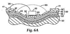
図6A〜7を見てみると、コンプライアント基板30の代表的な断面図が示されており、このコンプライアント基板30は変形部を有し、この変形部の上又は中に、少なくとも1つのLEDダイが配置される。 Turning to FIGS. 6A-7, a representative cross-sectional view of a
図6Aでは、パターンニング済みのコンプライアント基板30が変形して、凹部の底面にLEDダイ20を受容するのに十分なサイズの凹部(図5Aの凹部70のようなもの)が形成されている。上記の通り、LEDダイ20を第1の導電層32に取り付けるのに用いることのできる取り付け方法は、導電性接着剤、異方導電性接着剤、又は、はんだリフローなどである。図示されている実施形態では、熱放散アセンブリ50が所望の凹部とともに予め形成されており、基板30が、基板30と熱放散アセンブリ50との間で厚みが比較的一定である熱界面材の層52によって、熱放散アセンブリ50に合わせて取り付けられる。任意のカプセル材90が、LEDダイ20を覆うように図示されている。 In FIG. 6A, the patterned
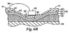
図6Bは、図6Aのものと類似した照明アセンブリの一部を示すが、熱放散アセンブリ50は実質的に平らな表面を有しており、この平らな表面に基板30は取り付けられる。熱界面材の層52は、凹部70によって変位しているとともに、基板30の形状に適合している。層52の縮小厚によって、熱界面材の層からの熱インピーダンスが低下する。 FIG. 6B shows a portion of a lighting assembly similar to that of FIG. 6A, but the
図6Cもまた、図6Aのものと類似する照明アセンブリの一部を示すが、凹部30(depression 30)の深さがLEDダイ20の高さよりも大きい。図6Cの実施形態では、任意のカプセル材90が、基板30の上面と実質的に重なって凹部70を埋め尽くすように描かれており、このアセンブリとともに、拡散フィルム、偏向フィルム(3M社(3M Company)から入手可能な「ビキュイティ(Vikuiti)(商標)DBEFフィルム」のうちのいずれかなど)などの1つ以上の任意の光学フィルム92、又は、構造化表面フィルム(3M社(3M Company)から入手可能な「ビキュイティ(Vikuiti)(商標)BEFフィルム」のうちのいずれかなど)が用いられる。別の実施形態では、凹部70は、カプセル材90を全く有さなくてもよく、又は、カプセル材90の一部を有してもよい。 6C also shows a portion of the lighting assembly similar to that of FIG. 6A, but the depth of the
図7を見てみると、パターニング済みのコンプライアント基板30が変形して、突出部80が形成されている。上記の通り、LEDダイ20を第1の導電層32に取り付けるのに用いることのできる取り付け方法は、導電性接着剤、異方導電性接着剤、又は、はんだリフローなどである。熱放散アセンブリ50は、基板30が取り付けられている実質的に平らな表面を有し、熱界面材の層52は、基板30の変形形状に適合している。別の実施形態では、熱放散アセンブリは、突出部80の所望の形状物とともに予め形成されることができ、基板30は、熱界面材の層52によって熱放散アセンブリ50に合わせて取り付けることができる。 As shown in FIG. 7, the patterned
本明細書に記載されている代表的な実施形態は、既知のカプセル材及び/又は既知の光学フィルムと組み合わせて用いる場合に、とりわけ有用である。例えば、リン光層(色変換用)を有するか、又は別の形でリン光体を含むカプセル材を、LEDダイの光出力を低下させることなく、LEDダイ20の上又は周囲で用いることができる。カプセル材は、いずれかの形状又は構成を有する基板30内の変形部、例えば、基板30の上面34の下に延びている変形部、及び、基板30の上面34の上に突き出ている変形部などと併せて用いることができる。 The exemplary embodiments described herein are particularly useful when used in combination with known encapsulants and / or known optical films. For example, an encapsulant having a phosphor layer (for color conversion) or otherwise containing a phosphor may be used on or around the LED die 20 without reducing the light output of the LED die. it can. The encapsulant is a deformed portion in the
図8を見てみると、照明アセンブリ10の製造時には、コンプライアント基板を供給ロール100から巻き出すなどすることによって、上記のコンプライアント基板30を供給するとともに、第1の導電層32をパターニングステーション102でパターニングして、所望の回路トレース41を形成する。層32のパターニングは、従来の回路構築技術のいずれかを用いて実現してもよい。LEDダイ20は、上記の通り既知及び従来のダイ取り付け法及びワイヤボンディング法を用いて、ダイ取り付けステーション104でパターニング済みの第1の導電層32に取り付けられる。続いて、LEDダイ20を有するコンプライアント基板30を成形ステーション106で変形させて、基板30に所望の表面特徴部(すなわち凹部、突出部、又は、これらの組み合わせ)を供給するとともに、LEDダイ20の位置に対応する位置にこれらの表面特徴部を配置する。次に、任意に応じてカプセル材90をカプセルステーション108で適用し、その後、硬化させてから、LEDダイ20を有する基板30を巻き取りロール110に巻き付ける。別のケースでは、コンプライアント基板30の変形は、成形ステーション106’によって図示されているように、LEDダイ20を取り付ける前に行うことができる。一部のケースでは、巻き取りロール110に巻き付ける代わりに、LEDダイ20を有する基板30を間隔を置いて切断して、例えば、バックライト式ディスプレイ、看板、又は、グラフィックにおいて用いるものとして、バックライト内に実装するのに適した、複数の照明アセンブリストリップ、パネル、又はその他の形状物を供給する。更に別のケースでは、巻き取りロール110は、次の加工工程の供給ロールになることができる。 Referring to FIG. 8, when the
LEDダイ20を有する基板30の変形は、多種多様な技術を用いて実現させてよい。ある1つの技術では、コンプライアント基板内に、所望の形状の鈍器を1つ以上手で押し付けて、所望の凹部又は突出部を形成する。別の技術では、LEDダイ20又はその電気相互接続部を損傷させないように構成されたツールを用いて、LEDダイ20を有する基板30をエンボス又はスタンピング加工する。好ましくは、1つ以上の所望の変形部を有する成形されたツールが供給される。コンプライアント基板を、一連の1つ以上の位置に、ツールに相対させて配置し、ツールをこのコンプライアント基板の上に押し付け、それによって、所望のパターンで基板を変形させる。スタンピング作業では、空気圧、機械的手段、油圧、又は、当該技術分野において既知の物体をスタンピング加工、エンボス加工、又は、コイニング加工するその他の方法を用いることができる。 The deformation of the
所望に応じて、LEDダイ20を有する基板30は、所望の特徴部を備えている支持面(熱放散アセンブリ50など)に合わせて取り付けることができる。この支持面は、基板30をその支持面に接着する前に、部分的又は完全に、基板30の所望の最終形状に形成されてもよく、あるいは、支持面は、基板30を変形させて所望の表面特徴部を作るのと同時に形成されてもよい。基板30を支持面の表面特徴部に成形又は変形させることは、真空モールド/プレス加工、又は、ラミネート加工(加熱及び/又は加圧の有無は問わない)などの技術を用いて実現してもよい。 If desired, the
開示したコンプライアント基板は、上記のLEDダイのみならず、その他の回路コンポーネント、特にかなりの熱を発生するコンポーネントとともにも用いることができる。したがって、本発明者は、上で開示したものと類似の照明アセンブリを考慮しているが、LEDダイの一部又は全部は、有機発光ダイオード(OLED)、固体レーザー、パワートランジスタ、集積回路(IC)、及び、有機エレクトロニクスのうちの1つ以上によって置き換えられる。 The disclosed compliant substrate can be used not only with the LED die described above, but also with other circuit components, particularly those that generate significant heat. The inventor therefore contemplates lighting assemblies similar to those disclosed above, but some or all of the LED dies may be organic light emitting diodes (OLEDs), solid state lasers, power transistors, integrated circuits (ICs). ) And one or more of the organic electronics.
別段の指示がない限り、本明細書及び「特許請求の範囲」で用いる数量、特性の測定値などを表す全ての数値は、いかなる場合も、「約」という語で修飾されているものとして理解されるべきである。したがって、これに反する指示がない限り、上記の明細書及び添付の「特許請求の範囲」に記載されている数値パラメータは、本発明の教示を利用する当業者が得ようとする望ましい特性に応じて変更可能な概算値である。最低でも、特許請求の範囲への同等物の原則の適用を限定する試みとしてではなく、少なくとも各数値的パラメータは、報告されている有効数字の数を考慮して、通常の四捨五入の適用によって解釈しなければならない。広範にわたる本発明の範囲で示す数値的範囲及びパラメータは概算値であるが、具体例に記載の数値は可能な範囲で正確に報告されている。しかし、いずれの数値にも、それらの各試験測定値において見られる標準偏差から必然的に生じる特定の誤差が本質的に含まれている。 Unless otherwise indicated, all numerical values, such as quantities, property measurements, etc. used herein and in the claims, are understood as being modified by the word “about” in any case. It should be. Accordingly, unless indicated to the contrary, the numerical parameters set forth in the foregoing specification and attached claims are dependent upon the desired characteristics sought by those skilled in the art using the teachings of the invention. This is an approximate value that can be changed. At a minimum, each numerical parameter is interpreted by applying normal rounding, taking into account the number of significant figures reported, rather than as an attempt to limit the application of the equivalent principle to the claims. Must. Although the numerical ranges and parameters shown in the broad scope of the invention are approximate, the numerical values set forth in the specific examples are reported as accurately as possible. Any numerical value, however, inherently contains certain errors necessarily resulting from the standard deviation found in their respective testing measurements.
上記の記載は例示のためのものであり、本発明の範囲を限定する意図はない。本明細書に開示されている実施形態の変更及び修正は可能であり、当該技術分野の通常の技術を有する者であれば、本特許文書を読めば、本実施形態のさまざまな要素の実行可能な代替物及び同等物が分かるであろう。本発明の範囲及び精神を逸脱しないならば、本明細書に開示の実施形態の上記及びその他の変更及び修正を行ってもよい。 The above description is illustrative and is not intended to limit the scope of the invention. Variations and modifications of the embodiments disclosed herein are possible, and those skilled in the art will be able to implement the various elements of this embodiment by reading this patent document. Alternatives and equivalents will be appreciated. These and other changes and modifications to the embodiments disclosed herein may be made without departing from the scope and spirit of the invention.
図では、同様の要素には同様の参照数字が付されている。図は理想化されており、縮尺どおりには描かれておらず、また、例示のみを目的としたものである。 In the figure, like elements are given like reference numerals. The figures are idealized and are not drawn to scale and are for illustrative purposes only.
Claims (20)
Translated fromJapanese前記第1の導電フォイルの上に配置される複数のLEDダイと
を備える照明アセンブリ。A compliant substrate comprising first and second conductive foils separated by an electrically insulating layer, wherein the insulating layer comprises a polymer material filled with particles that increase the thermal conductivity of the insulating layer. A client substrate,
A plurality of LED dies disposed on the first conductive foil.
前記ヒートシンクと前記第2の導電フォイルとの間に配置される熱界面材の層と組み合わされる、請求項1に記載のアセンブリ。The assembly of claim 1, in combination with a heat sink; and a layer of thermal interface material disposed between the heat sink and the second conductive foil.
電気絶縁層で隔てられている第1及び第2の導電フォイルを備えるコンプライアント基板を供給する工程;
前記第1の導電フォイルをパターニングする工程;
複数のLEDダイを前記パターニング済みの第1の導電フォイルに取り付ける工程;及び
前記基板を永久変形させて、複数の表面特徴部を画定する工程を含み、前記表面特徴部の位置がLEDダイの位置に対応する、方法。A method for manufacturing a lighting assembly comprising:
Providing a compliant substrate comprising first and second conductive foils separated by an electrically insulating layer;
Patterning the first conductive foil;
Attaching a plurality of LED dies to the patterned first conductive foil; and permanently deforming the substrate to define a plurality of surface features, wherein the position of the surface features is a position of the LED die Corresponding to the method.
Applications Claiming Priority (2)
| Application Number | Priority Date | Filing Date | Title |
|---|---|---|---|
| US74319506P | 2006-01-31 | 2006-01-31 | |
| PCT/US2007/002195WO2007089599A2 (en) | 2006-01-31 | 2007-01-26 | Led illumination assembly with compliant foil construction |
Publications (2)
| Publication Number | Publication Date |
|---|---|
| JP2009525614Atrue JP2009525614A (en) | 2009-07-09 |
| JP2009525614A5 JP2009525614A5 (en) | 2010-03-18 |
Family
ID=38137663
Family Applications (1)
| Application Number | Title | Priority Date | Filing Date |
|---|---|---|---|
| JP2008553272AWithdrawnJP2009525614A (en) | 2006-01-31 | 2007-01-26 | LED lighting assembly having compliant foil structure |
Country Status (7)
| Country | Link |
|---|---|
| US (1) | US7572031B2 (en) |
| EP (1) | EP1996860A2 (en) |
| JP (1) | JP2009525614A (en) |
| KR (1) | KR101347486B1 (en) |
| CN (1) | CN101379344B (en) |
| TW (1) | TW200734750A (en) |
| WO (1) | WO2007089599A2 (en) |
Cited By (11)
| Publication number | Priority date | Publication date | Assignee | Title |
|---|---|---|---|---|
| JP2009545863A (en)* | 2006-08-04 | 2009-12-24 | オスラム オプト セミコンダクターズ ゲゼルシャフト ミット ベシュレンクテル ハフツング | Thin film semiconductor component and component combination |
| JP2011129932A (en)* | 2009-12-21 | 2011-06-30 | Lg Innotek Co Ltd | Light emitting device and light unit employing the same |
| JP2011222875A (en)* | 2010-04-13 | 2011-11-04 | Sony Chemical & Information Device Corp | Light-reflective, anisotropic and conductive adhesive, and light-emitting device |
| JP2014132629A (en)* | 2012-12-07 | 2014-07-17 | Toshiba Lighting & Technology Corp | Light-emitting device and light device |
| KR20140124551A (en)* | 2013-04-17 | 2014-10-27 | 엘지이노텍 주식회사 | lighting emitting device |
| JP2014531109A (en)* | 2011-08-29 | 2014-11-20 | コーニンクレッカ フィリップス エヌ ヴェ | A flexible lighting assembly, a luminaire, and a method of manufacturing a flexible layer. |
| US9231177B2 (en) | 2013-07-01 | 2016-01-05 | Nichia Corporation | Light emitting device |
| JP2017524262A (en)* | 2014-08-08 | 2017-08-24 | コーニンクレッカ フィリップス エヌ ヴェKoninklijke Philips N.V. | LED device with flexible thermal interface |
| JP2017152450A (en)* | 2016-02-22 | 2017-08-31 | 大日本印刷株式会社 | LED display device |
| KR20190091310A (en)* | 2016-11-30 | 2019-08-05 | 택토텍 오와이 | Light emitting structure and method of manufacturing the same |
| JP2021057578A (en)* | 2019-09-27 | 2021-04-08 | シーメンス アクチエンゲゼルシヤフトSiemens Aktiengesellschaft | Circuit board, package and method for its production |
Families Citing this family (43)
| Publication number | Priority date | Publication date | Assignee | Title |
|---|---|---|---|---|
| US9951438B2 (en) | 2006-03-07 | 2018-04-24 | Samsung Electronics Co., Ltd. | Compositions, optical component, system including an optical component, devices, and other products |
| KR20080006304A (en)* | 2006-07-12 | 2008-01-16 | 삼성전자주식회사 | OLED display and manufacturing method thereof |
| US8439252B2 (en)* | 2006-11-07 | 2013-05-14 | Excelitas Technologies Gmbh & Co Kg | Method for bonding metal surfaces, method for producing an object having cavities, object having cavities, structure of a light emitting diode |
| WO2009014590A2 (en) | 2007-06-25 | 2009-01-29 | Qd Vision, Inc. | Compositions and methods including depositing nanomaterial |
| WO2009014707A2 (en) | 2007-07-23 | 2009-01-29 | Qd Vision, Inc. | Quantum dot light enhancement substrate and lighting device including same |
| DE102007043904A1 (en)* | 2007-09-14 | 2009-03-19 | Osram Gesellschaft mit beschränkter Haftung | Luminous device |
| DE102007043903A1 (en)* | 2007-09-14 | 2009-03-26 | Osram Gesellschaft mit beschränkter Haftung | Luminous device |
| DE102007046520A1 (en)* | 2007-09-28 | 2009-04-02 | Osram Opto Semiconductors Gmbh | Light-emitting surface element and method for producing a light-emitting surface element |
| WO2009137053A1 (en) | 2008-05-06 | 2009-11-12 | Qd Vision, Inc. | Optical components, systems including an optical component, and devices |
| WO2009151515A1 (en) | 2008-05-06 | 2009-12-17 | Qd Vision, Inc. | Solid state lighting devices including quantum confined semiconductor nanoparticles |
| US9207385B2 (en) | 2008-05-06 | 2015-12-08 | Qd Vision, Inc. | Lighting systems and devices including same |
| US8022626B2 (en)* | 2008-09-16 | 2011-09-20 | Osram Sylvania Inc. | Lighting module |
| DE102009019412A1 (en) | 2009-04-29 | 2010-11-04 | Fa. Austria Technologie & Systemtechnik Ag | Method for producing a printed circuit board with LEDs and printed reflector surface and printed circuit board, produced by the method |
| CN102598313B (en) | 2009-08-14 | 2016-03-23 | Qd视光有限公司 | Light emitting device, optical element for light emitting device, and method |
| US9797580B2 (en)* | 2010-05-24 | 2017-10-24 | Abl Ip Holding Llc | LED light fixture |
| JP2014503607A (en) | 2010-11-03 | 2014-02-13 | スリーエム イノベイティブ プロパティズ カンパニー | Polymer etching agent and method of using the same |
| KR20130143061A (en) | 2010-11-03 | 2013-12-30 | 쓰리엠 이노베이티브 프로퍼티즈 컴파니 | Flexible led device with wire bond free die |
| US9698563B2 (en) | 2010-11-03 | 2017-07-04 | 3M Innovative Properties Company | Flexible LED device and method of making |
| GB2484152B (en)* | 2010-12-03 | 2015-03-25 | Zeta Specialist Lighting | Methods of manufacturing electrical devices such as electric lamps |
| US8912562B2 (en) | 2010-12-29 | 2014-12-16 | 3M Innovative Properties Company | Remote phosphor LED constructions |
| US9151463B2 (en) | 2010-12-29 | 2015-10-06 | 3M Innovative Properties Company | LED color combiner |
| US9232634B2 (en) | 2011-01-17 | 2016-01-05 | Canon Components, Inc. | Flexible circuit board for mounting light emitting element, illumination apparatus, and vehicle lighting apparatus |
| JP2013157592A (en)* | 2012-01-05 | 2013-08-15 | Canon Components Inc | Flexible circuit board for mounting light emitting element |
| USD668808S1 (en)* | 2011-05-27 | 2012-10-09 | BISS Product Development, LLC | Flexible task light |
| JP5228089B2 (en)* | 2011-07-06 | 2013-07-03 | シャープ株式会社 | Light emitting device and display device |
| JP5175956B2 (en)* | 2011-07-06 | 2013-04-03 | シャープ株式会社 | Light emitting device and display device |
| US8322906B2 (en) | 2011-08-08 | 2012-12-04 | XtraLight Manufacturing Partnership Ltd | Versatile lighting units |
| CN102612254A (en)* | 2011-08-10 | 2012-07-25 | 田茂福 | Heat radiation type LED (Light-Emitting Diode) flexible circuit board |
| DE102011086168B4 (en)* | 2011-11-11 | 2023-05-04 | Pictiva Displays International Limited | Organic light-emitting component and method for producing an organic optoelectronic component |
| US9929325B2 (en) | 2012-06-05 | 2018-03-27 | Samsung Electronics Co., Ltd. | Lighting device including quantum dots |
| US20140055991A1 (en)* | 2012-08-23 | 2014-02-27 | Forrest Starnes McCanless | Printed Circuit Boards with Deformations |
| CN103855142B (en)* | 2012-12-04 | 2017-12-29 | 东芝照明技术株式会社 | Light-emitting device and lighting device |
| US9091400B2 (en)* | 2013-01-30 | 2015-07-28 | Luxo-Led Co., Limited | Multi-color light emitting diode device |
| US9644829B2 (en) | 2013-04-25 | 2017-05-09 | Xtralight Manufacturing, Ltd. | Systems and methods for providing a field repairable light fixture with a housing that dissipates heat |
| US9335034B2 (en) | 2013-09-27 | 2016-05-10 | Osram Sylvania Inc | Flexible circuit board for electronic applications, light source containing same, and method of making |
| US10032753B2 (en)* | 2014-06-20 | 2018-07-24 | Grote Industries, Llc | Flexible lighting device having both visible and infrared light-emitting diodes |
| US10317614B1 (en)* | 2017-03-14 | 2019-06-11 | Automatad Assembly Corporation | SSL lighting apparatus |
| US10767840B2 (en) | 2017-05-01 | 2020-09-08 | Riverpoint Medical, Llc | Focused LED headlamp with iris assembly |
| US10174912B1 (en)* | 2017-05-01 | 2019-01-08 | R Iverpoint Medical, Llc | Focused LED headlamp with iris assembly |
| JP6898203B2 (en)* | 2017-10-27 | 2021-07-07 | 株式会社 日立パワーデバイス | Power semiconductor module |
| US10655823B1 (en) | 2019-02-04 | 2020-05-19 | Automated Assembly Corporation | SSL lighting apparatus |
| TWI784175B (en)* | 2019-06-14 | 2022-11-21 | 培英半導體有限公司 | Method for forming optical wall by laser engraving an opening and optical wall structure |
| US10995931B1 (en) | 2020-08-06 | 2021-05-04 | Automated Assembly Corporation | SSL lighting apparatus |
Family Cites Families (17)
| Publication number | Priority date | Publication date | Assignee | Title |
|---|---|---|---|---|
| JPH0437596A (en) | 1990-06-01 | 1992-02-07 | Toshiba Corp | Wiring board equipment |
| WO1996008047A2 (en)* | 1994-09-06 | 1996-03-14 | Philips Electronics N.V. | Electroluminescent device comprising a transparent structured electrode layer made from a conductive polymer |
| US6274224B1 (en) | 1999-02-01 | 2001-08-14 | 3M Innovative Properties Company | Passive electrical article, circuit articles thereof, and circuit articles comprising a passive electrical article |
| US6383005B2 (en) | 1999-12-07 | 2002-05-07 | Urex Precision, Inc. | Integrated circuit socket with contact pad |
| US6710456B1 (en)* | 2000-08-31 | 2004-03-23 | Micron Technology, Inc. | Composite interposer for BGA packages |
| US6799902B2 (en) | 2000-12-26 | 2004-10-05 | Emcore Corporation | Optoelectronic mounting structure |
| US6541800B2 (en) | 2001-02-22 | 2003-04-01 | Weldon Technologies, Inc. | High power LED |
| US6777870B2 (en) | 2001-06-29 | 2004-08-17 | Intel Corporation | Array of thermally conductive elements in an oled display |
| US6577492B2 (en) | 2001-07-10 | 2003-06-10 | 3M Innovative Properties Company | Capacitor having epoxy dielectric layer cured with aminophenylfluorenes |
| US20030063465A1 (en) | 2001-09-28 | 2003-04-03 | Mcmillan Richard K. | Etched metal light reflector for vehicle feature illumination |
| US6657297B1 (en) | 2002-08-15 | 2003-12-02 | The Bergquist Company | Flexible surface layer film for delivery of highly filled or low cross-linked thermally conductive interface pads |
| CN1601768A (en)* | 2003-09-22 | 2005-03-30 | 福建省苍乐电子企业有限公司 | LED structure |
| US20050116235A1 (en)* | 2003-12-02 | 2005-06-02 | Schultz John C. | Illumination assembly |
| DE102004016847A1 (en)* | 2004-04-07 | 2005-12-22 | P.M.C. Projekt Management Consult Gmbh | Light emitting diode arrangement and method for producing a light emitting diode array |
| US7997771B2 (en) | 2004-06-01 | 2011-08-16 | 3M Innovative Properties Company | LED array systems |
| US7201497B2 (en) | 2004-07-15 | 2007-04-10 | Lumination, Llc | Led lighting system with reflective board |
| US7303315B2 (en) | 2004-11-05 | 2007-12-04 | 3M Innovative Properties Company | Illumination assembly using circuitized strips |
- 2007
- 2007-01-26JPJP2008553272Apatent/JP2009525614A/ennot_activeWithdrawn
- 2007-01-26KRKR1020087018759Apatent/KR101347486B1/ennot_activeExpired - Fee Related
- 2007-01-26CNCN200780004037XApatent/CN101379344B/ennot_activeExpired - Fee Related
- 2007-01-26WOPCT/US2007/002195patent/WO2007089599A2/enactiveApplication Filing
- 2007-01-26EPEP07762789Apatent/EP1996860A2/ennot_activeWithdrawn
- 2007-01-30TWTW096103377Apatent/TW200734750A/enunknown
- 2007-01-31USUS11/669,622patent/US7572031B2/ennot_activeExpired - Fee Related
Cited By (16)
| Publication number | Priority date | Publication date | Assignee | Title |
|---|---|---|---|---|
| US8872330B2 (en) | 2006-08-04 | 2014-10-28 | Osram Opto Semiconductors Gmbh | Thin-film semiconductor component and component assembly |
| JP2009545863A (en)* | 2006-08-04 | 2009-12-24 | オスラム オプト セミコンダクターズ ゲゼルシャフト ミット ベシュレンクテル ハフツング | Thin film semiconductor component and component combination |
| JP2011129932A (en)* | 2009-12-21 | 2011-06-30 | Lg Innotek Co Ltd | Light emitting device and light unit employing the same |
| JP2011222875A (en)* | 2010-04-13 | 2011-11-04 | Sony Chemical & Information Device Corp | Light-reflective, anisotropic and conductive adhesive, and light-emitting device |
| JP2014531109A (en)* | 2011-08-29 | 2014-11-20 | コーニンクレッカ フィリップス エヌ ヴェ | A flexible lighting assembly, a luminaire, and a method of manufacturing a flexible layer. |
| JP2014132629A (en)* | 2012-12-07 | 2014-07-17 | Toshiba Lighting & Technology Corp | Light-emitting device and light device |
| KR102026120B1 (en)* | 2013-04-17 | 2019-11-04 | 엘지이노텍 주식회사 | lighting emitting device |
| KR20140124551A (en)* | 2013-04-17 | 2014-10-27 | 엘지이노텍 주식회사 | lighting emitting device |
| US9231177B2 (en) | 2013-07-01 | 2016-01-05 | Nichia Corporation | Light emitting device |
| JP2017524262A (en)* | 2014-08-08 | 2017-08-24 | コーニンクレッカ フィリップス エヌ ヴェKoninklijke Philips N.V. | LED device with flexible thermal interface |
| JP2017152450A (en)* | 2016-02-22 | 2017-08-31 | 大日本印刷株式会社 | LED display device |
| KR20190091310A (en)* | 2016-11-30 | 2019-08-05 | 택토텍 오와이 | Light emitting structure and method of manufacturing the same |
| JP2020507178A (en)* | 2016-11-30 | 2020-03-05 | タクトテク オーユー | Lighting structure and related manufacturing method |
| JP7129975B2 (en) | 2016-11-30 | 2022-09-02 | タクトテク オーユー | Lighting structure and associated manufacturing method |
| KR102604257B1 (en) | 2016-11-30 | 2023-11-20 | 택토텍 오와이 | Light-emitting structure and method of manufacturing the same |
| JP2021057578A (en)* | 2019-09-27 | 2021-04-08 | シーメンス アクチエンゲゼルシヤフトSiemens Aktiengesellschaft | Circuit board, package and method for its production |
Also Published As
| Publication number | Publication date |
|---|---|
| TW200734750A (en) | 2007-09-16 |
| US7572031B2 (en) | 2009-08-11 |
| KR101347486B1 (en) | 2014-01-02 |
| WO2007089599A2 (en) | 2007-08-09 |
| KR20080091784A (en) | 2008-10-14 |
| EP1996860A2 (en) | 2008-12-03 |
| CN101379344A (en) | 2009-03-04 |
| CN101379344B (en) | 2013-08-28 |
| WO2007089599A3 (en) | 2007-12-13 |
| US20070177380A1 (en) | 2007-08-02 |
Similar Documents
| Publication | Publication Date | Title |
|---|---|---|
| KR101347486B1 (en) | LED Illumination Assembly With Compliant Foil Construction | |
| US7806560B2 (en) | LED illumination assembly with compliant foil construction | |
| US6828170B2 (en) | Method of making a semiconductor radiation emitter package | |
| EP2365550B1 (en) | Light emitting diode package | |
| US8530915B2 (en) | Power surface mount light emitting die package | |
| US9698563B2 (en) | Flexible LED device and method of making | |
| JP5520243B2 (en) | Power surface mounted light emitting die package | |
| US8519427B2 (en) | Light emitting device and lighting system | |
| US20130037830A1 (en) | Light emitting diode package and method for manufacturing the same | |
| KR20080106242A (en) | Lighting assembly with improved thermal conductivity | |
| US9608172B2 (en) | Optoelectronic semiconductor component | |
| KR20110138757A (en) | Light emitting element | |
| KR101129002B1 (en) | Optical package and manufacturing method of the same | |
| KR20130079939A (en) | Light emitting device, light emitting devicd package and light emitting module | |
| TWI542031B (en) | Optical package and method of manufacturing same | |
| KR101250372B1 (en) | Optical component package and manufacturing method thereof | |
| KR101168420B1 (en) | Tpae type light emitting diode package and manufacturing method of the same | |
| KR20130118446A (en) | Substrate and light emitting device module having the same |
Legal Events
| Date | Code | Title | Description |
|---|---|---|---|
| A521 | Request for written amendment filed | Free format text:JAPANESE INTERMEDIATE CODE: A523 Effective date:20100126 | |
| A621 | Written request for application examination | Free format text:JAPANESE INTERMEDIATE CODE: A621 Effective date:20100126 | |
| A761 | Written withdrawal of application | Free format text:JAPANESE INTERMEDIATE CODE: A761 Effective date:20110620 |