JP2009508324A6 - Microelectronic device, stacked microelectronic device, and method of manufacturing microelectronic device - Google Patents
Microelectronic device, stacked microelectronic device, and method of manufacturing microelectronic deviceDownload PDFInfo
- Publication number
- JP2009508324A6 JP2009508324A6JP2008526996AJP2008526996AJP2009508324A6JP 2009508324 A6JP2009508324 A6JP 2009508324A6JP 2008526996 AJP2008526996 AJP 2008526996AJP 2008526996 AJP2008526996 AJP 2008526996AJP 2009508324 A6JP2009508324 A6JP 2009508324A6
- Authority
- JP
- Japan
- Prior art keywords
- microelectronic
- contacts
- interposer substrate
- substrate
- die
- Prior art date
- Legal status (The legal status is an assumption and is not a legal conclusion. Google has not performed a legal analysis and makes no representation as to the accuracy of the status listed.)
- Pending
Links
- 238000004377microelectronicMethods0.000titleclaimsabstractdescription435
- 238000004519manufacturing processMethods0.000titleclaimsdescription23
- 239000000758substrateSubstances0.000claimsabstractdescription334
- 230000008878couplingEffects0.000claimsabstractdescription47
- 238000010168coupling processMethods0.000claimsabstractdescription47
- 238000005859coupling reactionMethods0.000claimsabstractdescription47
- 238000000034methodMethods0.000claimsabstractdescription41
- 230000000712assemblyEffects0.000claimsdescription3
- 238000000429assemblyMethods0.000claimsdescription3
- 238000003491arrayMethods0.000claims3
- 238000010586diagramMethods0.000description23
- 230000008901benefitEffects0.000description7
- 239000000853adhesiveSubstances0.000description6
- 230000001070adhesive effectEffects0.000description6
- 229910000679solderInorganic materials0.000description6
- 230000008569processEffects0.000description3
- 230000007613environmental effectEffects0.000description2
- 239000000463materialSubstances0.000description2
- 229920001690polydopaminePolymers0.000description2
- 239000004593EpoxySubstances0.000description1
- 239000002313adhesive filmSubstances0.000description1
- 238000005229chemical vapour depositionMethods0.000description1
- 230000002950deficientEffects0.000description1
- 238000000151depositionMethods0.000description1
- 230000008021depositionEffects0.000description1
- 230000005611electricityEffects0.000description1
- 238000005538encapsulationMethods0.000description1
- 239000003344environmental pollutantSubstances0.000description1
- 238000005530etchingMethods0.000description1
- 238000002513implantationMethods0.000description1
- 238000001746injection mouldingMethods0.000description1
- 238000012986modificationMethods0.000description1
- 230000004048modificationEffects0.000description1
- 238000000465mouldingMethods0.000description1
- 238000004806packaging method and processMethods0.000description1
- 238000000206photolithographyMethods0.000description1
- 238000007747platingMethods0.000description1
- 231100000719pollutantToxicity0.000description1
- 238000003908quality control methodMethods0.000description1
- 230000003068static effectEffects0.000description1
- 238000003860storageMethods0.000description1
- 239000000126substanceSubstances0.000description1
- -1tapeSubstances0.000description1
Images


Abstract
Translated fromJapaneseDescription
Translated fromJapanese本発明は、マイクロ電子デバイス、積み重ねられたマイクロ電子デバイス、およびマイクロ電子デバイスを製造する方法に関する。 The present invention relates to microelectronic devices, stacked microelectronic devices, and methods of manufacturing microelectronic devices.
マイクロ電子デバイスは、一般にダイ(すなわち、チップ)を有し、それは非常に小さな部品が高度に密集する集積回路を含む。典型的なプロセスでは、様々な段階で反復することのできる多くの異なる方法(例えば、注入、ドーピング、フォトリソグラフィ、化学気相成長法、プラズマ蒸着、メッキ、平坦化、エッチング、など)を用いて、多数のダイが単一のウエハ上に製造される。ダイは、一般に、集積回路と電気的に接続される非常に小さなボンドパッドのアレイを含む。ボンドパッドはダイ上の外部電気接触部であり、それを通じて電源電圧、信号などが集積回路へ伝送され、また集積回路から伝送される。次に、ウエハをさいの目(またはダイ)に切断することにより、ダイをお互いに分離(すなわち、単一化)し、個々のダイを裏面研削する。ダイが単一化された後、ダイは、一般に「パッケージ化」され、ボンドパッドは、様々な電力供給線、信号線、および接地線により容易に結合することのできるさらに大きな電気端子のアレイと結合される。 Microelectronic devices typically have a die (ie, a chip) that includes an integrated circuit in which very small components are highly dense. A typical process uses many different methods (eg, implantation, doping, photolithography, chemical vapor deposition, plasma deposition, plating, planarization, etching, etc.) that can be repeated at various stages. Multiple dies are fabricated on a single wafer. The die typically includes an array of very small bond pads that are electrically connected to the integrated circuit. The bond pad is an external electrical contact on the die through which power supply voltages, signals, etc. are transmitted to and from the integrated circuit. The wafer is then cut into dice (or dies) to separate the dies from one another (ie, singulate) and the individual dies are back ground. After the die has been singulated, the die is generally “packaged” and the bond pads have a larger array of electrical terminals that can be easily coupled by various power supply lines, signal lines, and ground lines. Combined.
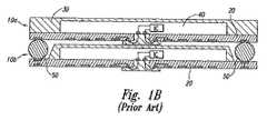
個別のダイは、ダイ上のボンドパッドをピン、ボールパッド、またはその他の種類の電気端子のアレイと電気的に接続すること、および次に環境要因(例えば、湿度、微粒子、静電気、および物理的衝撃)から保護するためにダイを封入することによりパッケージ化することができる。一用途では、ボンドパッドは、ボールパッドのアレイを有するインターポーザ基板上のコンタクトと電気的に接続される。図1Aは、従来のパッケージ化されたマイクロ電子デバイス10を図で説明したもので、それにはインターポーザ基板20およびインターポーザ基板20に取り付けられるマイクロ電子ダイ40が含まれる。マイクロ電子ダイ40は、ダイ40を環境要因から保護するためにケーシング30で封入されている。 Individual dies are used to electrically connect bond pads on the die to an array of pins, ball pads, or other types of electrical terminals, and then environmental factors (eg, humidity, particulates, static electricity, and physical It can be packaged by encapsulating the die to protect it from impact). In one application, the bond pads are electrically connected with contacts on an interposer substrate having an array of ball pads. FIG. 1A illustrates a conventional packaged
電気製品は、非常に限られた空間に極めて高密度の部品を有するようパッケージ化されたマイクロ電子デバイスを必要とする。例えば、記憶装置、プロセッサ、ディスプレイ、およびその他のマイクロ電子部品に使用可能な空間は、携帯電話、PDA、ポータブルコンピュータ、および多くのその他の製品では非常に限られている。そのようなものとして、プリント回路基板上のマイクロ電子デバイス10の表面積または「占有面積」を減少させたいという強い動因がある。マイクロ電子デバイス10のサイズを小さくすることは、高性能マイクロ電子デバイス10が一般により多くのボンドパッドを有し、ボンドパッドが多いと、ボールグリッドアレイがより大きくなり、それ故により占有面積が大きくなるために困難である。所与の占有面積内でマイクロ電子デバイス10の密度を増大させるために用いられる一つの技術は、マイクロ電子デバイス10をもう一つのデバイスの上に積み重ねることである。 Electrical products require microelectronic devices that are packaged to have very high density components in a very limited space. For example, the space available for storage devices, processors, displays, and other microelectronic components is very limited in cell phones, PDAs, portable computers, and many other products. As such, there is a strong drive to reduce the surface area or “occupied area” of the
図1Bは、同様の第2のマイクロ電子デバイス10bの上に積み重ねられた、図1Aのパッケージ化されたマイクロ電子デバイス(10aとして識別される)を図で説明したものである。第1のマイクロ電子デバイス10aのインターポーザ(または介在)基板20は、大きなはんだボール50により第2のマイクロ電子デバイス10bのインターポーザ基板20に結合されている。積み重ねられたデバイス10a〜10bの一つの欠点は、2つのインターポーザ基板20間の距離をつなぐために必要な大きなはんだボール50がインターポーザ基板20上の貴重な空間を使用し、マイクロ電子デバイス10a〜10bの
占有面積を増大させていることである。FIG. 1B graphically illustrates the packaged microelectronic device of FIG. 1A (identified as 10a) stacked on a similar second microelectronic device 10b. The interposer (or intervening)
図2は、先行技術に従うもう1つのパッケージ化されたマイクロ電子デバイス60を図で説明したものである。デバイス60は、基板80に取り付けられる第1のマイクロ電子ダイ70aおよび第1のダイ70aに取り付けられる第2のマイクロ電子ダイ70bを含む。第1および第2のダイ70a〜70bは、複数個のワイヤボンド90で基板80と電気的に接続される。このデバイスはダイ70a〜70bおよびワイヤボンド90を封入しているケーシング95をさらに含む。図2に説明されるパッケージ化されたマイクロ電子デバイス60の一つの欠点は、ダイ70a〜70bのうちの1つが、基板80に適切にワイヤボンディングされていないかまたはその他の何らかの理由でカプセル封入後の品質管理試験で不合格となる場合、良好なダイ70を含む、パッケージ化されたデバイス60は一般に廃棄されることである。従って、複数のダイを一緒に封入すると、得られるパッケージの収率が低下する。 FIG. 2 diagrammatically illustrates another packaged
A.概説
以下の開示は、マイクロ電子デバイス、積み重ねられたマイクロ電子デバイス、およびマイクロ電子デバイスを製造する方法のいくつかの実施形態を説明する。1つのそのような一組の積み重ねられたマイクロ電子デバイスの実施形態は、(a)第1の面および第1の面と反対側の第2の面を有する第1のマイクロ電子ダイ、(b)第1のマイクロ電子ダイの第1の面と取り付けられ、第1のマイクロ電子ダイと電気的に接続される第1の基板、(c)第1のマイクロ電子ダイの第2の面に取り付けられる第2の基板、(d)第2の基板に取り付けられる複数個の電気的結合体(またはカップラー)、(e)電気的結合体に結合される第3の基板、および(f)第3の基板に取り付けられる第2のマイクロ電子ダイを含む。電気的結合体は、電気的結合体の少なくとも一部が第1のマイクロ電子ダイの内側になるように配置される。A. The following disclosure describes several embodiments of microelectronic devices, stacked microelectronic devices, and methods of manufacturing microelectronic devices. One such set of stacked microelectronic device embodiments includes: (a) a first microelectronic die having a first surface and a second surface opposite the first surface; A) a first substrate attached to the first surface of the first microelectronic die and electrically connected to the first microelectronic die; and (c) attached to a second surface of the first microelectronic die. (D) a plurality of electrical couplings (or couplers) attached to the second substrate, (e) a third substrate coupled to the electrical couplings, and (f) a third A second microelectronic die attached to the substrate. The electrical coupling body is arranged such that at least a part of the electrical coupling body is inside the first microelectronic die.
本発明のもう一つの態様は、マイクロ電子デバイスに向けられる。一実施形態では、マイクロ電子デバイスは、(a)第1の面、第1の面と反対側の第2の面、集積回路、および集積回路と電気的に接続される複数個の端子を有するマイクロ電子ダイ、(b)マイクロ電子ダイの第1の面に結合される第1のインターポーザ基板、および(c)マイクロ電子ダイの第2の面に結合される第2のインターポーザ基板を含む。第1のインターポーザ基板は、複数個の第1のコンタクトと複数個の第2のコンタクトを有する。第1のコンタクトは対応する端子と電気的に接続される。第2のインターポーザ基板は第1のインターポーザ基板の対応する第2のコンタクトと電気的に接続される複数個のコンタクトを有する。 Another aspect of the invention is directed to a microelectronic device. In one embodiment, the microelectronic device has (a) a first surface, a second surface opposite the first surface, an integrated circuit, and a plurality of terminals electrically connected to the integrated circuit. A microelectronic die, (b) a first interposer substrate coupled to the first surface of the microelectronic die, and (c) a second interposer substrate coupled to the second surface of the microelectronic die. The first interposer substrate has a plurality of first contacts and a plurality of second contacts. The first contact is electrically connected to the corresponding terminal. The second interposer substrate has a plurality of contacts that are electrically connected to corresponding second contacts of the first interposer substrate.
本発明のもう一つの態様は、複数個のマイクロ電子デバイスを製造する方法に向けられる。一実施形態では、方法は、複数個のマイクロ電子ダイを、ダイをアレイに配置して第1のインターポーザ基板に実装すること、マイクロ電子ダイを第1のインターポーザ基板と関連する第2のインターポーザ基板との間に位置付けて、複数個の第2のインターポーザ基板を対応するマイクロ電子ダイに取り付けること、および第2のインターポーザ基板と第1のインターポーザ基板を電気的に接続することを含む。 Another aspect of the invention is directed to a method of manufacturing a plurality of microelectronic devices. In one embodiment, a method includes mounting a plurality of microelectronic dies on a first interposer substrate with the dies arranged in an array, a second interposer substrate associated with the microelectronic die. And attaching a plurality of second interposer substrates to corresponding microelectronic dies, and electrically connecting the second interposer substrate and the first interposer substrate.
本発明のもう一つの態様は、マイクロ電子デバイスを積み重ねる方法に向けられる。一実施形態では、方法は、(a)マイクロ電子ダイ、マイクロ電子ダイに結合される第1のインターポーザ基板、および、ダイが第1のインターポーザ基板と第2のインターポーザ基板との間に位置するように、マイクロ電子ダイに結合される第2のインターポーザ基板を有する第1のマイクロ電子デバイスを提供すること、(b)マイクロ電子ダイおよびマイクロ電子ダイに結合されるインターポーザ基板を有する第2のマイクロ電子デバイスを
提供すること、および(c)複数個の電気的結合体を第1のマイクロ電子デバイスと第2のマイクロ電子デバイスとの間であって、第1のマイクロ電子デバイスのダイの内側に位置付けて、第1のマイクロ電子デバイスの上に第2のマイクロ電子デバイスを積み重ねることを含む。例えば、電気的結合体を第1のマイクロ電子デバイスのマイクロ電子ダイに対して重ね合わせ、ダイの外辺部内の区域に位置付けてよい。Another aspect of the invention is directed to a method of stacking microelectronic devices. In one embodiment, the method includes: (a) a microelectronic die, a first interposer substrate coupled to the microelectronic die, and the die positioned between the first interposer substrate and the second interposer substrate. Providing a first microelectronic device having a second interposer substrate coupled to the microelectronic die; (b) a second microelectronic having a microelectronic die and an interposer substrate coupled to the microelectronic die. Providing a device; and (c) positioning a plurality of electrical couplings between the first microelectronic device and the second microelectronic device inside the die of the first microelectronic device. And stacking a second microelectronic device on top of the first microelectronic device. For example, the electrical combination may be superimposed on the microelectronic die of the first microelectronic device and positioned in an area within the outer periphery of the die.
本発明のいくつかの実施形態の多くの具体的な詳細は、複数個のマイクロ電子デバイスを一緒に単一のアセンブリに形成することに関して下に記載されているが、その他の実施形態では各デバイスを別々に形成することもできる。本発明の特定の実施形態の十分な理解をもたらすため、本発明に従ういくつかの実施形態が、図3A〜図7および以下の文章に説明される。しかし、当業者であれば、本発明がさらなる実施形態を有しうること、または本発明が図3A〜図7に示される実施形態の詳細のいくつかを含まなくとも実践されうることを理解する。 Many specific details of some embodiments of the invention are described below with respect to forming a plurality of microelectronic devices together in a single assembly, while in other embodiments, each device Can also be formed separately. In order to provide a thorough understanding of certain embodiments of the present invention, several embodiments according to the present invention are described in FIGS. 3A-7 and the following text. However, those skilled in the art will appreciate that the present invention may have further embodiments or that the present invention may be practiced without including some of the details of the embodiments shown in FIGS. 3A-7. .
B.マイクロ電子デバイスを製造する方法の実施形態
図3A〜図3Dは、複数個のマイクロ電子デバイスを製造する方法の一実施形態の段階を説明する。例えば、図3Aは、第1のインターポーザ基板120上でアレイに配置される複数個のマイクロ電子ダイ110(3個のみが示されている)を含むアセンブリ100の垂直断面の略図である。個別のダイ110は、集積回路112(図示される)、作動面114、作動面114上でアレイに配置される複数個の端子116(例えば、ボンドパッド)、および作動面114の反対側の裏面118を含む。ダイ110の裏面118は、接着剤130、例えば接着フィルム、エポキシ、テープ、ペースト、またはその他の適した材料などで第1のインターポーザ基板120に取り付けられる。図示したダイ110は同じ構造を有するが、その他の実施形態では、ダイ110は、異なる機能を実行するために異なる特徴を有していてよい。B. Embodiment of Method for Manufacturing Microelectronic Device FIGS. 3A-3D illustrate the steps of one embodiment of a method for manufacturing a plurality of microelectronic devices. For example, FIG. 3A is a schematic diagram of a vertical section of an
第1のインターポーザ基板120は、プリント基板であっても、ダイ110を支持するためのその他の部材であってもよい。図解される実施形態では、第1のインターポーザ基板120は、(a)複数個の第1のコンタクト126と複数個の第2のコンタクト127を有する第1の面122、および(b)複数個のパッド128を有する第2の面124を含む。第1のコンタクト126は、ダイ110上の対応する端子116との電気的接続のためにアレイに配置することができ、第2のコンタクト127は、第2のインターポーザ基板上の対応するコンタクトとの電気的接続のためにアレイに配置することができ(図3Bに示す)、さらに、パッド128は、アレイに配置して複数個の電気的結合体(例えば、はんだボール)を受けることができる。第1のインターポーザ基板120は、第1および第2のコンタクト126および127を対応するパッド128と電気的に接続する複数個の導電トレース129をさらに含む。 The
図3Bは、複数個の第2のインターポーザ基板140を対応するマイクロ電子ダイ110に取り付けた後のアセンブリ100の垂直断面の略図である。個々の第2のインターポーザ基板140は、第1の面142および接着剤132でダイ110の1つに取り付けられる第2の面144を含む。第1の面142は、(a)第1のインターポーザ基板120上の第2のコンタクト127の対応するアレイと電気的接続するためにアレイに配置される複数個のコンタクト146、および(b)複数個の電気的結合体(例えば、はんだボール)への取り付けのためにアレイに配置される複数個のパッド148を含む。いくつかの実施形態では、図3Dに関して下に説明されるように、マイクロ電子デバイスが同様のデバイスの上に積み重ねられ、複数個の電気的結合体が対応するパッド128および148の組を電気的に接続することができるように、パッド148は、一般に第1のインターポーザ基板120上の対応するパッド128と一直線に並んでいる。個別の第2のインター
ポーザ基板140は、パッド148と対応するコンタクト146を電気的に接続する複数個の導電トレース149をさらに含む。図示される第2のインターポーザ基板140の占有面積は個別のダイ110の占有面積よりも小さいが、その他の実施形態、例えば図4に関して下に記載される実施形態では、第2のインターポーザ基板140の占有面積は、ダイ110の占有面積と同じまたはそれより大きいことがある。FIG. 3B is a schematic diagram of a vertical cross-section of
第2のインターポーザ基板140を取り付けた後、マイクロ電子ダイ110と第2のインターポーザ基板140は、第1のインターポーザ基板120にワイヤボンディングされる。具体的には、複数個の第1のワイヤボンド134をダイ110の端子116と第1のインターポーザ基板120上の対応する第1のコンタクト126との間に形成し、複数個の第2のワイヤボンド136を第2のインターポーザ基板140上のコンタクト146と第1のインターポーザ基板120上の対応する第2のコンタクト127との間に形成する。さらなる実施形態では、マイクロ電子ダイ110は、第2のインターポーザ基板140がダイ110に取り付けられる前に第1のインターポーザ基板120にワイヤボンディングされ得る。その他の実施形態では、第2のインターポーザ基板140は、ダイ110が第1のインターポーザ基板120に取り付けられる前にダイ110に取り付けられ得る。 After attaching the
図3Cは、ケーシング150を形成し、複数個の電気的結合体160を取り付けた後のアセンブリ100の垂直断面の略図である。ケーシング150は、マイクロ電子ダイ110、第1および第2のワイヤボンド134および136、ならびに第1および第2のインターポーザ基板120および140の一部を封入する。具体的には、図示されるケーシング150は、第2のインターポーザ基板140の第1の面142の外辺部分をコンタクト146が覆われるように封入し、第2のインターポーザ基板140の第1の面142の中心部分の上の開口部152をパッド148が露出するように画定する。ケーシング150は、従来の射出成形、フィルム成形、またはその他の適した方法により形成することができる。ケーシング150を形成した後、電気的結合体160を第1のインターポーザ基板120上の対応するパッド128に取り付け、アセンブリ100をA−Aの線に沿って切断して複数個の個々のマイクロ電子デバイス102を単一化することができる。 FIG. 3C is a schematic diagram of a vertical cross section of the
図3Dは、下側のマイクロ電子デバイス102bの上に積み重ねられた上側のマイクロ電子デバイス102aの垂直断面の略図である。上側および下側のデバイス102a〜102bは、一般に図3A〜図3Cに関して上に説明されるマイクロ電子デバイス102と同様である。上側のデバイス102aは、上側のデバイス102aの電気的結合体160を下側のデバイス102bのケーシング150の開口部152に挿入し、電気的結合体160を下側のデバイス102bの第2のインターポーザ基板140上の対応するパッド148に取り付けることにより、下側のデバイス102bと結合される。その他の実施形態では、上側および下側のデバイス102a〜102bは異なるデバイスであってよい。例えば、上側のデバイス102aには第2のインターポーザ基板140および第2のワイヤボンド136が含まれないことがある。さらに、上側および下側のマイクロ電子デバイス102a〜102b中のマイクロ電子ダイ110は、同じ種類のダイであっても異なる種類のダイであってもよい。その他の実施形態では、さらなるマイクロ電子デバイスを上側のデバイス102aの上に、および/または下側のデバイス102bの下に積み重ねることができる。さらなる実施形態では、マイクロ電子デバイス102は、アセンブリが切断され、デバイス102が単一化される前に積み重ねることができる。例えば、複数個の単一化されたデバイス102は、図3Cに図示されるアセンブリ100の対応するデバイス102に取り付けることができる。あるいは、2つ以上のアセンブリのデバイス102を取り付け、一緒に単一化することができる。 FIG. 3D is a schematic diagram of a vertical cross section of the upper microelectronic device 102a stacked on the lower microelectronic device 102b. The upper and lower devices 102a-102b are generally similar to the
図3A〜図3Dに関して上に説明されるマイクロ電子デバイス102の一つの利点は、デバイス102を互いの上に積み重ねることができることである。マイクロ電子デバイス
を積み重ねることにより回路基板の所与の表面積または占有面積内での能力および/または性能が増大する。例えば、上側のマイクロ電子デバイス102aを下側のマイクロ電子デバイス102bの上に積み重ね、下側のデバイス102bを回路基板に取り付ける場合、上側のマイクロ電子デバイス102aは回路基板上の表面積をあまり多く使用することなく電気的にかつ作動可能なように回路基板に結合される。One advantage of the
図3A〜図3Dに示されるマイクロ電子デバイス102のもう一つの特徴は、パッケージ化の後および積み重ねる前に個別のデバイスを試験することができることである。この特徴の利点は、欠点のあるパッケージ化されたデバイスを検出し、デバイスの積み重ねから排除することができることである。したがって、マイクロ電子デバイスの積み重ねは優良であるとわかっているデバイスのみを含むことができ、それによりデバイスの積み重ね収率が増大し、廃棄されるデバイスの数が減少する。 Another feature of the
図3Dに示される積み重ねられたマイクロ電子デバイス102のもう一つの特徴は、下側のマイクロ電子デバイス102bが、ダイ110の内側に複数個の露出したパッド148をもつ第2のインターポーザ基板140を含むことである。この特徴の利点は、上側のマイクロ電子デバイス102aが完全に装着されたボールグリッドアレイを含み得ることであり、それにより回路基板上の占有面積を増大させることなく上側のデバイス102aから回路基板へ伝えることのできる信号の数が増加する。 Another feature of the stacked
C.マイクロ電子デバイスのさらなる実施形態およびマイクロ電子デバイスを製造する方法
図4は、本発明のもう1つの実施形態に従うマイクロ電子デバイス202の垂直断面の略図である。マイクロ電子デバイス202は、一般に、図3A〜図3Dに関して上に説明されるマイクロ電子デバイス102と同様である。例えば、マイクロ電子デバイス202は、第1のインターポーザ基板120に取り付けられるマイクロ電子ダイ110を含む。しかし、図示されるマイクロ電子デバイス202は、スタンドオフ270によりダイ110から離れて間隔を空けられた第2のインターポーザ基板240をさらに含む。第2のインターポーザ基板240は、(a)複数個のコンタクト246と複数個のパッド248を有する第1の面242、および(b)第1の面242の反対側の第2の面244を含む。コンタクト246はアレイに配置され、複数個の第2のワイヤボンド136で第1のインターポーザ基板120上の対応する第2のコンタクト127と電気的に接続される。パッド248は、アレイに配置され、第1のインターポーザ基板120上の対応するパッド128と一直線に並び得る。図示される第2のインターポーザ基板240の占有面積はダイ110の占有面積とほぼ同じであるが、その他の実施形態では、第2のインターポーザ基板240の占有面積は、ダイ110の占有面積よりも大きくてもよいし、小さくてもよい。C. Further Embodiments of Microelectronic Device and Method for Manufacturing Microelectronic Device FIG. 4 is a schematic diagram of a vertical cross-section of a
スタンドオフ270は、第2のインターポーザ基板240の第2の面244に第1の接着剤232aで、さらにダイ110の作動面114に第2の接着剤232bで取り付けられる。スタンドオフ270は、第2のインターポーザ基板240にダイ110から間隔を空ける大きさに作られているので第1のワイヤボンド134を端子116と第1のインターポーザ基板120上の対応する第1のコンタクト126との間に伸ばすことができる。スタンドオフ270は、鏡面ウエハ、テープ、ペースト、またはその他の適したデバイスであってよい。ケーシング250は第2のインターポーザ基板240とマイクロ電子ダイ110との間の空隙を埋めることができる。 The
図4に示されるマイクロ電子デバイス202の一つの特徴は、第2のインターポーザ基板240の占有面積が、図3A〜図3Dに関して上に考察される第2のインターポーザ基板140よりも大きいことである。この特徴の利点は、図示される第2のインターポーザ
基板240がより多くのパッド248を含み、より大きなボールグリッドアレイを収めることができることであり、それによりデバイスの積み重ねにおいて上側のマイクロ電子デバイスから下側のマイクロ電子デバイスへ伝えることのできる信号の数が増加する。One feature of the
図5A〜図5Cは、複数個のマイクロ電子デバイスを製造する方法のもう1つの実施形態の段階を説明する。例えば、図5Aは、第1のインターポーザ基板120上にアレイに配置される複数個のマイクロ電子ダイ310(3個のみが示されている)を含むアセンブリ300の垂直断面の略図である。個々のマイクロ電子ダイ310は、集積積回路112(図示される)、作動面314、作動面314上でアレイに配置される複数個の端子316、および作動面314の反対側の裏面318を含む。マイクロ電子ダイ310の裏面318は、接着剤130で第1のインターポーザ基板120に取り付けられる。第1のインターポーザ基板120は、一般に、図3A〜図3Dに関して上に説明される第1のインターポーザ基板120と同様である。 5A-5C illustrate the steps of another embodiment of a method of manufacturing a plurality of microelectronic devices. For example, FIG. 5A is a schematic diagram of a vertical cross section of an
図5Bは、複数個の第2のインターポーザ基板340を、配線素子370で対応するマイクロ電子ダイ310に取り付けた後のアセンブリ300の垂直断面の略図である。個々の第2のインターポーザ基板340は、第1の面342、第1の面342の反対側の第2の面344、第1の面342上の複数個の第1のコンタクト345、第1の面342上の複数個の第2のコンタクト346、第2の面344上の複数個の第3のコンタクト347、および第1の面342上の複数個のパッド348を含む。第1のコンタクト345は、第1のインターポーザ基板120上の対応する第1のコンタクト126との電気接続のためにアレイに配置され、第2のコンタクト346は、第1のインターポーザ基板120上の対応する第2のコンタクト127との電気的接続のためにアレイに配置され、第3のコンタクト347は、アレイに配置され、対応する配線素子370に取り付けられ、さらに、パッド348は、複数個の電気的結合体への取り付けのためにアレイに配置される。第2のインターポーザ基板340は、第1のコンタクト345と対応する第3のコンタクト347を電気的に接続する複数個の第1の導電トレース349a、および第2のコンタクト346と対応するパッド348を電気的に接続する複数個の第2の導電トレース349bをさらに含み得る。配線素子370は、はんだボールであってもよいし、またはマイクロ電子ダイ310の端子316を第2のインターポーザ基板340上の対応する第3のコンタクト347と電気的に接続するその他の導電部材であってもよい。アセンブリ300に、さらにアンダーフィル材372をマイクロ電子ダイ310と対応する第2のインターポーザ基板340との間に含めて、部品に加わる一部の応力に耐え、部品を湿度、化学薬品、およびその他の汚染物質から保護することもできる。 FIG. 5B is a schematic diagram of a vertical cross section of
図5Cは、第2のインターポーザ基板340を第1のインターポーザ基板120にワイヤボンディングし、ケーシング350を形成した後のアセンブリ300の垂直断面の略図である。複数個の第1のワイヤボンド334は、第2のインターポーザ基板340の第1のコンタクト345と第1のインターポーザ基板120上の対応する第1のコンタクト126との間に伸び、複数個の第2のワイヤボンド335は、第2のインターポーザ基板340の第2のコンタクト346と第1のインターポーザ基板120上の対応する第2のコンタクト127との間に伸びる。第1および第2のワイヤボンド334および335は、従ってマイクロ電子ダイ310の端子316および第2のインターポーザ基板340のパッド348を、それぞれ、第1のインターポーザ基板120のパッド128と電気的に接続する。 FIG. 5C is a schematic diagram of a vertical cross section of
ケーシング350は、マイクロ電子ダイ310ならびに第1および第2のインターポーザ基板120および340の一部を封入する。具体的には、ケーシング350は、第2のインターポーザ基板340の外辺部を、第1および第2のコンタクト345および346が封入され、パッド348が露出するように封入する。ケーシング350の形成後、アセ
ンブリ300を線B−Bに沿って切断して複数個の個々のマイクロ電子デバイス302を単一化することができる。The
図6A〜図6Eは、複数個のマイクロ電子デバイスを製造する方法のもう1つの実施形態の段階を説明する。例えば、図6Aは、第1のインターポーザ基板420上にアレイに配置される複数個のマイクロ電子ダイ410(3個のみが示されている)を含むアセンブリ400の垂直断面の略図である。個々のマイクロ電子ダイ410は、集積回路112、第1のインターポーザ基板420に取り付けられる作動面414、作動面414上の複数個の端子416、および作動面414の反対側の裏面418を含む。 6A-6E illustrate steps of another embodiment of a method of manufacturing a plurality of microelectronic devices. For example, FIG. 6A is a schematic diagram of a vertical cross section of an
図示される第1のインターポーザ基板420は、第1の面422、第1の面422の反対側の第2の面424、第1の面422上の複数個の第1のコンタクト426、第2の面424上の複数個の第2のコンタクト427、第2の面424上の複数個の第1のパッド428a、第2の面424上の複数個の第2のパッド428b、および第1の面422と第2の面424の間に伸びる複数個のスロット425を含む。第1のコンタクト426は、第2のインターポーザ基板上の対応するコンタクトとの電気接続のためにアレイに配置され(下に図6Bに関して説明されている)、第2のコンタクト427は、ダイ410上の対応する端子416との電気接続のためにアレイに配置され、さらに、第1および第2のパッド428a〜428bは、複数個の電気的結合体を受けるためにアレイに配置されている。第1のインターポーザ基板420は、第1のコンタクト426と対応する第1のパッド428aを電気的に接続する複数個の第1の導電トレース429a、および、第2のコンタクト427と対応する第2のパッド428bを電気的に接続する複数個の第2の導電トレース429bをさらに含む。 The illustrated
図6Bは、複数個の第2のインターポーザ基板440を対応するダイ410に接着剤432で取り付けた後のアセンブリ400の垂直断面の略図である。第2のインターポーザ基板440は、第1の面442、ダイ410の1つに取り付けられる第2の面444、第1の面442上の複数個のコンタクト446、第1の面442上の複数個のパッド448、およびコンタクト446と対応するパッド448を電気的に接続する複数個の導電トレース449を含む。パッド448は、電気的結合体への取り付けのためにアレイに配置され、一般に第1のインターポーザ基板420上の対応するパッド428と一直線に並び得る。図示される第2のインターポーザ基板440の占有面積はダイ410の占有面積とほぼ同じであるが、その他の実施形態では、第2のインターポーザ基板の占有面積は、ダイ410の占有面積よりも大きくてもよいし、小さくてもよい。 FIG. 6B is a schematic illustration of a vertical cross section of
第2のインターポーザ基板440をダイ410に取り付けた後、ダイ410は第1のインターポーザ基板420にワイヤボンディングされ、第1のインターポーザ基板420は第2のインターポーザ基板440にワイヤボンディングされる。具体的には、複数個の第1のワイヤボンド434がダイ410の端子416を第1のインターポーザ基板420上の対応する第2のコンタクト427に電気的に接続し、複数個の第2のワイヤボンド436が第2のインターポーザ基板440上のコンタクト446を第1のインターポーザ基板420上の対応する第1のコンタクト426に電気的に接続する。 After attaching the
図6Cは、ケーシング450を形成した後のアセンブリ400の垂直断面の略図である。ケーシング450は、マイクロ電子ダイ410、第1および第2のワイヤボンド434および436、ならびに第1および第2のインターポーザ基板420および440の一部を封入する。具体的には、ケーシング450は、個々の第2のインターポーザ基板440の外辺部を、コンタクト446がケーシング450に覆われるが、パッド448が露出するように封入する。そのようなものとして、ケーシング450は、もう一つのマイクロ電子デバイスから電気的結合体を受けるための開口部452を規定する。ケーシング450
はまた、第2のコンタクト427および第1のインターポーザ基板420中のスロット425を覆う。ケーシング450を形成した後、複数個の電気的結合体460を第1のインターポーザ基板420の対応するパッド428に置くことができ、アセンブリ400を線C−Cに沿って切断して複数個の個々のデバイス402を単一化することができる。FIG. 6C is a schematic illustration of a vertical cross section of
Also covers the
図6Dは、下側のマイクロ電子デバイス402bの上に積み重ねられた上側のマイクロ電子デバイス402aの垂直断面の略図である。上側のデバイス402aは、上側のデバイス402aの電気的結合体460を下側のデバイス402bのケーシング450の開口部452に挿入し、電気的結合体460を下側のデバイス402bの第2のインターポーザ基板440上の対応するパッド448に取り付けることにより、下側のデバイス402bと結合される。 FIG. 6D is a schematic diagram of a vertical cross-section of the upper microelectronic device 402a stacked on the lower
図6A〜図6Dに示されるマイクロ電子デバイス402の一つの特徴は、電気的結合体460がマイクロ電子ダイ410の内側に位置することである。この特徴の利点は、デバイス402の占有面積が縮小されることである。その一方、先行技術のデバイス、例えば図1Aおよび1Bに示されるデバイス10a〜10bでは、はんだボール50がダイ40の外側に位置しており、そしてその結果、デバイス10a〜10bは図6A〜図6Dに示されるマイクロ電子デバイス402よりも大きい占有面積を有する。より大きな占有面積を有するデバイスは、携帯電話、PDA、コンピュータ、およびその他の製品におけるプリント回路基板およびその他の基板により多くの空間を使用する。 One feature of the
図7は、本発明のもう1つの実施形態に従うマイクロ電子デバイス502の垂直断面の略図である。マイクロ電子デバイス502は、一般に、図6A〜図6Dに関して上に説明されるマイクロ電子デバイス402と同様である。例えば、図示されるマイクロ電子デバイス502は、第1のインターポーザ基板520と第2のインターポーザ基板540との間に取り付けられるマイクロ電子ダイ410を含む。しかし、図示される実施形態では、第1のインターポーザ基板520は第2の面424上の複数個の第1のコンタクトを含み、第2のインターポーザ基板540は第2の面444上の複数個のコンタクト546を含む。さらに、図示される第2のインターポーザ基板540は、ダイ410および第1のインターポーザ基板520よりも大きな占有面積を有する。図示されるマイクロ電子デバイス502は、(a)第2のインターポーザ基板540上のコンタクト546と第1のインターポーザ基板520上の対応する第1のコンタクト526との間に伸びる複数個の第2のワイヤボンド536、および(b)第1および第2のワイヤボンド434および536を封入しているケーシング550をさらに含む。 FIG. 7 is a schematic diagram of a vertical cross-section of a
図7に示されるマイクロ電子デバイス502の一つの特徴は、第1および第2のワイヤボンド434および536がデバイス502の単一の面に形成されることである。この特徴の利点は、両方の面にワイヤボンドを形成するためにデバイスを裏返すことを必要とする処理よりも迅速かつ容易な単一パス処理で、マイクロ電子デバイス502をワイヤボンディングすることができることである。図7に示されるマイクロ電子デバイス502のもう一つの特徴は、ケーシング550が第2のインターポーザ基板540の単一の面だけに形成されることである。この特徴の利点は、ケーシング550を、2面の金型キャビティよりも複雑でなく安価な片側だけの金型キャビティを用いて形成することができることである。 One feature of the
前述の内容から、本発明の特定の実施形態が説明を目的として本明細書に記載されるが、本発明の精神および範囲から逸脱することなく様々な変更形態がなされうることは当然理解される。例えば、一実施形態の要素の多くは、他の実施形態の要素に加えて、あるいは他の実施形態の要素の代わりに他の実施形態と組み合わせることができる。従って、本発明は付属の特許請求の範囲に限定される場合を除き、限定されない。 From the foregoing, it will be understood that although specific embodiments of the invention have been described herein for purposes of illustration, various modifications may be made without departing from the spirit and scope of the invention. . For example, many of the elements of one embodiment can be combined with other embodiments in addition to or in place of elements of other embodiments. Accordingly, the invention is not limited except as by the appended claims.
図6A〜図6Dは、複数個のマイクロ電子デバイスを製造する方法のもう1つの実施形態の段階を説明する。例えば、図6Aは、第1のインターポーザ基板420上にアレイに配置される複数個のマイクロ電子ダイ410(3個のみが示されている)を含むアセンブリ400の垂直断面の略図である。個々のマイクロ電子ダイ410は、集積回路112、第1のインターポーザ基板420に取り付けられる作動面414、作動面414上の複数個の端子416、および作動面414の反対側の裏面418を含む。FIG 6A~ Figure 6D illustrates the steps of another embodiment of a method of manufacturing a plurality of microelectronic devices. For example, FIG. 6A is a schematic diagram of a vertical cross section of an
Claims (66)
Translated fromJapanese前記第1のマイクロ電子ダイの前記第1の面に取り付けられ、前記第1のマイクロ電子ダイと電気的に接続される第1の基板と、
前記第1のマイクロ電子ダイの前記第2の面に取り付けられる第2の基板と、
前記第2の基板に取り付けられ、複数個の電気的結合体の少なくとも一部が前記第1のマイクロ電子ダイの内側に位置する複数個の電気的結合体と、
前記複数個の電気的結合体に結合される第3の基板と、
前記第3の基板に取り付けられる第2のマイクロ電子ダイとを含む、一組の積み重ねられた複数個のマイクロ電子デバイス。A first microelectronic die including a first surface and a second surface opposite the first surface;
A first substrate attached to the first surface of the first microelectronic die and electrically connected to the first microelectronic die;
A second substrate attached to the second surface of the first microelectronic die;
A plurality of electrical assemblies attached to the second substrate, wherein at least some of the plurality of electrical assemblies are located inside the first microelectronic die; and
A third substrate coupled to the plurality of electrical couplers;
A set of stacked microelectronic devices including a second microelectronic die attached to the third substrate.
前記第1のマイクロ電子ダイが、さらに複数個の端子を前記作動面に含み、
前記第1の基板が、前記第1のマイクロ電子ダイの前記裏面に取り付けられる第1の面、前記第1の面上の複数個の第1のコンタクト、および前記第1の面上の複数個の第2のコンタクトを含み、
前記第2の基板が、対応する複数個の電気的結合体に取り付けられる複数個のパッドおよび対応する複数個のパッドと電気的に接続される複数個のコンタクトを含み、ならびに
前記複数個のマイクロ電子デバイスが(a)前記第1のマイクロ電子ダイ上の前記複数個の端子と前記第1の基板上の対応する複数個の第1のコンタクトを電気的に接続する複数個の第1のワイヤボンド、(b)前記第2の基板上の前記複数個のコンタクトと前記第1の基板上の対応する複数個の第2のコンタクトを電気的に接続する複数個の第2のワイヤボンド、および(c)前記第2の基板と前記第1のマイクロ電子ダイとの間のスタンドオフをさらに含む、請求項1に記載の複数個のマイクロ電子デバイス。The first surface of the first microelectronic die includes a back surface, the second surface of the first microelectronic die includes an operating surface;
The first microelectronic die further includes a plurality of terminals on the working surface;
The first substrate is attached to the back surface of the first microelectronic die, a first surface, a plurality of first contacts on the first surface, and a plurality of on the first surface. A second contact of
The second substrate includes a plurality of pads attached to the corresponding plurality of electrical coupling bodies and a plurality of contacts electrically connected to the corresponding plurality of pads; An electronic device (a) a plurality of first wires that electrically connect the plurality of terminals on the first microelectronic die and a corresponding plurality of first contacts on the first substrate; (B) a plurality of second wire bonds for electrically connecting the plurality of contacts on the second substrate and a corresponding plurality of second contacts on the first substrate; The plurality of microelectronic devices of claim 1, further comprising (c) a standoff between the second substrate and the first microelectronic die.
前記第1のマイクロ電子ダイが複数個の端子を前記作動面上にさらに含み、
前記第1の基板が前記第1のマイクロ電子ダイの前記作動面に取り付けられる第1の面、前記第1の面と反対側の第2の面、前記第1および第2の面の間に伸びる開口部、および前記第2の面上の複数個のコンタクトを含み、ならびに
前記複数個のマイクロ電子デバイスが、前記複数個の端子と対応する複数個のコンタクトを電気的に接続する複数個のワイヤボンドをさらに含む、請求項1に記載の複数個のマイクロ電子デバイス。The first surface of the first microelectronic die includes an actuation surface;
The first microelectronic die further includes a plurality of terminals on the working surface;
A first surface on which the first substrate is attached to the working surface of the first microelectronic die, a second surface opposite to the first surface, and between the first and second surfaces A plurality of contacts on the second surface, and the plurality of microelectronic devices electrically connect the plurality of contacts corresponding to the plurality of terminals. The plurality of microelectronic devices of claim 1, further comprising a wire bond.
前記第1のマイクロ電子ダイが複数個の端子を前記作動面上にさらに含み、
前記第1の基板が、前記第1のマイクロ電子ダイの前記作動面に取り付けられる第1の面、前記第1の面と反対側の第2の面、前記第1および第2の面の間に伸びる開口部、前記第1の面上の複数個の第1のコンタクト、および前記第2の面上の複数個の第2のコンタクトを含み、
前記第2の基板が、対応する複数個の電気的結合体に取り付けられる複数個のパッドおよび対応する複数個のパッドと電気的に接続される複数個のコンタクトを含み、ならびに
前記複数個のマイクロ電子デバイスが、(a)前記第1のマイクロ電子ダイ上の前記複数個の端子と前記第1の基板上の対応する複数個の第2のコンタクトを電気的に接続する複数個の第1のワイヤボンド、および(b)前記第2の基板上の前記複数個のコンタクトを前記第1の基板上の対応する複数個の第1のコンタクトと電気的に接続する複数個の第2のワイヤボンドをさらに含む、請求項1に記載の複数個のマイクロ電子デバイス。The first surface of the first microelectronic die includes a working surface, and the second surface of the first microelectronic die includes a back surface;
The first microelectronic die further includes a plurality of terminals on the working surface;
The first substrate is attached to the operating surface of the first microelectronic die, the second surface opposite to the first surface, and between the first and second surfaces. An opening extending to the first surface, a plurality of first contacts on the first surface, and a plurality of second contacts on the second surface;
The second substrate includes a plurality of pads attached to the corresponding plurality of electrical coupling bodies and a plurality of contacts electrically connected to the corresponding plurality of pads; An electronic device comprises: (a) a plurality of first electrical connections electrically connecting the plurality of terminals on the first microelectronic die and a corresponding plurality of second contacts on the first substrate. A wire bond; and (b) a plurality of second wire bonds that electrically connect the plurality of contacts on the second substrate with a corresponding plurality of first contacts on the first substrate. The plurality of microelectronic devices of claim 1, further comprising:
前記第1のマイクロ電子ダイが複数個の端子を前記作動面上にさらに含み、
前記第1の基板が、前記第1のマイクロ電子ダイの前記裏面に取り付けられる第1の面と、前記第1の面上の複数個のコンタクトを含み、ならびに
前記複数個のマイクロ電子デバイスが、前記複数個の端子と対応する複数個のコンタクトを電気的に接続する複数個のワイヤボンドをさらに含む、請求項1に記載の複数個のマイクロ電子デバイス。The first surface of the first microelectronic die includes a back surface, the second surface of the first microelectronic die includes an operating surface;
The first microelectronic die further includes a plurality of terminals on the working surface;
The first substrate includes a first surface attached to the back surface of the first microelectronic die, a plurality of contacts on the first surface, and the plurality of microelectronic devices include: The plurality of microelectronic devices according to claim 1, further comprising a plurality of wire bonds that electrically connect a plurality of contacts corresponding to the plurality of terminals.
前記第1のマイクロ電子ダイが複数個の端子を前記作動面上にさらに含み、
前記第1の基板が、前記第1のマイクロ電子ダイの前記裏面に取り付けられる第1の面、前記第1の面上の複数個の第1のコンタクト、および前記第1の面上の複数個の第2のコンタクトを含み、
前記第2の基板が、対応する複数個の電気的結合体に取り付けられる複数個のパッドと、対応する複数個のパッドと電気的に接続される複数個のコンタクトを含み、ならびに
前記複数個のマイクロ電子デバイスが、(a)前記第1のマイクロ電子ダイ上の前記複数個の端子と前記第1の基板上の対応する複数個の第1のコンタクトを電気的に接続する複数個の第1のワイヤボンド、および(b)前記第2の基板上の前記複数個のコンタクトと前記第1の基板上の対応する複数個の第2のコンタクトを電気的に接続する複数個の第2のワイヤボンドをさらに含む、請求項1に記載の複数個のマイクロ電子デバイス。The first surface of the first microelectronic die includes a back surface, the second surface of the first microelectronic die includes an operating surface;
The first microelectronic die further includes a plurality of terminals on the working surface;
The first substrate is attached to the back surface of the first microelectronic die, a first surface, a plurality of first contacts on the first surface, and a plurality of on the first surface. A second contact of
The second substrate includes a plurality of pads attached to a corresponding plurality of electrical coupling bodies, a plurality of contacts electrically connected to the corresponding plurality of pads, and the plurality of the plurality of pads. A microelectronic device comprises: (a) a plurality of firsts that electrically connect the plurality of terminals on the first microelectronic die and a corresponding plurality of first contacts on the first substrate; And (b) a plurality of second wires for electrically connecting the plurality of contacts on the second substrate and a corresponding plurality of second contacts on the first substrate. The plurality of microelectronic devices of claim 1, further comprising a bond.
前記第1のマイクロ電子ダイが複数個の端子を前記作動面上にさらに含み、
前記第1の基板が前記第1のマイクロ電子ダイの前記裏面に取り付けられる第1の面および前記第1の面上の複数個のコンタクトを含み、
前記第2の基板が、前記第1のマイクロ電子ダイの前記作動面に面する第1の面、前記第1の面上の複数個の第1のコンタクト、および対応する複数個の第1のコンタクトと電気的に接続される複数個の第2のコンタクトを含み、かつ
前記複数個のマイクロ電子デバイスが、(a)前記第1のマイクロ電子ダイと前記第2の基板との間に位置し、前記複数個の端子と対応する複数個の第1のコンタクトを電気的に接続する複数個の電気的結合体、および(b)前記第2の基板上の前記複数個の第2のコンタクトと前記第1の基板上の対応する複数個のコンタクトを電気的に接続する複数個のワイヤボンドをさらに含む、請求項1に記載の複数個のマイクロ電子デバイス。The first surface of the first microelectronic die includes a back surface, the second surface of the first microelectronic die includes an operating surface;
The first microelectronic die further includes a plurality of terminals on the working surface;
The first substrate includes a first surface attached to the back surface of the first microelectronic die and a plurality of contacts on the first surface;
The second substrate has a first surface facing the working surface of the first microelectronic die, a plurality of first contacts on the first surface, and a corresponding plurality of first A plurality of second electronic contacts electrically connected to the contacts; and the plurality of microelectronic devices are (a) located between the first microelectronic die and the second substrate. A plurality of electrical coupling bodies that electrically connect the plurality of first contacts corresponding to the plurality of terminals; and (b) the plurality of second contacts on the second substrate; The plurality of microelectronic devices of claim 1, further comprising a plurality of wire bonds that electrically connect a corresponding plurality of contacts on the first substrate.
前記第1のマイクロ電子ダイが複数個の端子を前記作動面上にさらに含み、
前記第1の基板が、前記第1のマイクロ電子ダイの前記裏面に取り付けられる第1の面および前記第1の面上の複数個のコンタクトを含み、
前記第2の基板が、前記第1のマイクロ電子ダイの前記作動面に面する第1の面、前記第1の面と反対側の第2の面、前記第1の面上の複数個の第1のコンタクト、対応する複数個の電気的結合体に取り付けられる前記第2の面上の複数個の第2のコンタクト、および複数個の第3のコンタクトを含み、ならびに
前記複数個のマイクロ電子デバイスが、(a)前記第1のマイクロ電子ダイと前記第2の基板との間に位置し、前記複数個の端子と対応する複数個の第1のコンタクトを電気的に接続する複数個の配線素子、および(b)前記第2の基板上の前記複数個の第3のコン
タクトと前記第1の基板上の対応する複数個のコンタクトを電気的に接続する複数個のワイヤボンドをさらに含む、請求項1に記載の複数個のマイクロ電子デバイス。The first surface of the first microelectronic die includes a back surface, the second surface of the first microelectronic die includes an operating surface;
The first microelectronic die further includes a plurality of terminals on the working surface;
The first substrate includes a first surface attached to the back surface of the first microelectronic die and a plurality of contacts on the first surface;
The second substrate includes a first surface facing the operating surface of the first microelectronic die, a second surface opposite to the first surface, and a plurality of surfaces on the first surface. Including a first contact, a plurality of second contacts on the second surface attached to a corresponding plurality of electrical couplings, and a plurality of third contacts, and the plurality of microelectronics A plurality of devices (a) positioned between the first microelectronic die and the second substrate and electrically connecting a plurality of first contacts corresponding to the plurality of terminals; A wiring element; and (b) a plurality of wire bonds that electrically connect the plurality of third contacts on the second substrate and the corresponding contacts on the first substrate. A plurality of microelectronic devices according to claim 1 .
前記第3の基板が複数個のコンタクトを含み、および
前記複数個の電気的結合体が前記第2の基板の前記複数個のコンタクトと前記第3の基板の対応する複数個のコンタクトを電気的に接続する複数個の導電性ボールを含む、請求項1に記載の複数個のマイクロ電子デバイス。The second substrate includes a plurality of contacts;
The third substrate includes a plurality of contacts, and the plurality of electrical couplings electrically connect the plurality of contacts of the second substrate and the corresponding contacts of the third substrate. The plurality of microelectronic devices according to claim 1, comprising a plurality of conductive balls connected to the.
前記複数個のマイクロ電子デバイスが、前記第2のマイクロ電子ダイの前記第2の面に取り付けられる第4の基板をさらに含む、請求項1に記載の複数個のマイクロ電子デバイス。The second microelectronic die includes a first surface attached to the third substrate and a second surface opposite to the first surface, and the plurality of microelectronic devices includes the first surface The plurality of microelectronic devices of claim 1, further comprising a fourth substrate attached to the second surface of two microelectronic dies.
前記複数個のマイクロ電子デバイスが、前記第1のマイクロ電子ダイ、前記第1の基板、および前記第2の基板の少なくとも一部を覆うケーシングをさらに含み、ならびに
前記ケーシングが、前記第2の基板の前記第2の面の切断部分を露出する開口部を規定する、請求項1に記載の複数個のマイクロ電子デバイス。The second substrate includes a first surface attached to the second surface of the first microelectronic die and a second surface opposite to the first surface;
The plurality of microelectronic devices further includes a casing covering at least a portion of the first microelectronic die, the first substrate, and the second substrate, and the casing includes the second substrate. The plurality of microelectronic devices of claim 1, wherein the microelectronic device defines an opening exposing a cut portion of the second surface.
前記第1の基板が、前記第1のマイクロ電子ダイの前記第1の面に取り付けられる第1の面、前記第1の面と反対側の第2の面、前記第2の面上の複数個のパッド、および対応する複数個のパッドと電気的に接続される複数個のコンタクトをさらに含み、
前記複数個の電気的結合体が、複数個の第1の電気的結合体を含み、ならびに
前記複数個のマイクロ電子デバイスが、対応する複数個のパッド上の複数個の第2の電気的結合体をさらに含む、請求項1に記載の複数個のマイクロ電子デバイス。The first microelectronic die further includes an integrated circuit and a plurality of terminals electrically connected to the integrated circuit;
The first substrate is a first surface attached to the first surface of the first microelectronic die, a second surface opposite to the first surface, and a plurality of surfaces on the second surface. And a plurality of contacts electrically connected to the corresponding pads and the corresponding plurality of pads,
The plurality of electrical couplings includes a plurality of first electrical couplings, and the plurality of microelectronic devices includes a plurality of second electrical couplings on a corresponding plurality of pads. The plurality of microelectronic devices of claim 1, further comprising a body.
前記第1の基板が複数個のコンタクトをさらに含み、ならびに
前記複数個のマイクロ電子デバイスが、前記複数個の端子と対応する複数個のコンタクトを電気的に接続する複数個のワイヤボンドをさらに含む、請求項1に記載の複数個のマイクロ電子デバイス。The first microelectronic die further includes an integrated circuit and a plurality of terminals electrically connected to the integrated circuit;
The first substrate further includes a plurality of contacts, and the plurality of microelectronic devices further include a plurality of wire bonds that electrically connect the plurality of contacts corresponding to the plurality of terminals. A plurality of microelectronic devices according to claim 1.
前記第2の基板が複数個のコンタクトを含み、および
前記複数個のマイクロ電子デバイスが、前記第1の基板上の前記複数個のコンタクトと前記第2の基板上の対応する複数個のコンタクトを電気的に接続する複数個のワイヤボンドをさらに含む、請求項1に記載の複数個のマイクロ電子デバイス。The first substrate includes a plurality of contacts;
The second substrate includes a plurality of contacts; and the plurality of microelectronic devices includes the plurality of contacts on the first substrate and a corresponding plurality of contacts on the second substrate. The plurality of microelectronic devices of claim 1, further comprising a plurality of wire bonds that are electrically connected.
前記第1のマイクロ電子ダイが複数個の端子を前記作動面上にさらに含み、
前記第1の基板が、前記第1のマイクロ電子ダイの前記作動面に取り付けられる第1の面、前記第1の面と反対側の第2の面、前記第1および第2の面の間に伸びる開口部、前記第2の面上の複数個の第1のコンタクト、および前記第2の面上の複数個の第2のコンタクトを含み、
前記第2の基板が、対応する複数個の電気的結合体に取り付けられる複数個のパッド、および対応する複数個のパッドと電気的に接続される複数個のコンタクトを含み、ならびに
前記複数個のマイクロ電子デバイスが、(a)前記第1のマイクロ電子ダイ上の前記複数個の端子と前記第1の基板上の対応する複数個の第2のコンタクトを電気的に接続する複数個の第1のワイヤボンド、および(b)前記第2の基板上の前記複数個のコンタクトと前記第1の基板上の対応する複数個の第1のコンタクトを電気的に接続する複数個の第2のワイヤボンドをさらに含む、請求項1に記載の複数個のマイクロ電子デバイス。The first surface of the first microelectronic die includes a working surface, and the second surface of the first microelectronic die includes a back surface;
The first microelectronic die further includes a plurality of terminals on the working surface;
The first substrate is attached to the operating surface of the first microelectronic die, the second surface opposite to the first surface, and between the first and second surfaces. A plurality of first contacts on the second surface, and a plurality of second contacts on the second surface;
The second substrate includes a plurality of pads attached to a corresponding plurality of electrical coupling bodies, and a plurality of contacts electrically connected to the corresponding plurality of pads; The microelectronic device comprises: (a) a plurality of first terminals that electrically connect the plurality of terminals on the first microelectronic die and a corresponding plurality of second contacts on the first substrate. And (b) a plurality of second wires for electrically connecting the plurality of contacts on the second substrate and the corresponding plurality of first contacts on the first substrate. The plurality of microelectronic devices of claim 1, further comprising a bond.
前記第1のマイクロ電子ダイに取り付けられる第1のインターポーザ基板と、
前記第1のマイクロ電子ダイが前記第1のインターポーザ基板と第2のインターポーザ基板の間に位置するように、前記第1のマイクロ電子ダイに取り付けられる第2のインターポーザ基板と、
前記第2のインターポーザ基板が前記第1のマイクロ電子ダイと第3のインターポーザ基板の間に位置するように、前記第2のインターポーザ基板と結合される第3のインターポーザ基板とを含み、マイクロ電子ダイは前記第2のインターポーザ基板と第3のインターポーザ基板の間に位置せず、
前記第3のインターポーザ基板が第2のマイクロ電子ダイと前記第2のインターポーザ基板の間に位置するように、前記第3のインターポーザ基板に取り付けられる第2のマイクロ電子ダイとを含む、一組の積み重ねられた複数個のマイクロ電子デバイス。A first microelectronic die;
A first interposer substrate attached to the first microelectronic die;
A second interposer substrate attached to the first microelectronic die such that the first microelectronic die is located between the first interposer substrate and the second interposer substrate;
A third interposer substrate coupled to the second interposer substrate such that the second interposer substrate is positioned between the first microelectronic die and the third interposer substrate; Is not located between the second interposer substrate and the third interposer substrate,
A set of second microelectronic dies attached to the third interposer substrate such that the third interposer substrate is located between the second microelectronic die and the second interposer substrate. A plurality of stacked microelectronic devices.
前記第1のインターポーザ基板が、前記第1のマイクロ電子ダイの前記作動面に取り付けられる第1の面、前記第1の面と反対側の第2の面、前記第1および第2の面の間に伸びる開口部、および前記第2の面上の複数個のコンタクトを含み、ならびに
前記複数個のマイクロ電子デバイスが、前記複数個の端子と対応する複数個のコンタクトを電気的に接続する複数個のワイヤボンドをさらに含む、請求項20に記載の複数個のマイクロ電子デバイス。The first microelectronic die includes an operating surface and a plurality of terminals on the operating surface;
The first interposer substrate includes a first surface attached to the operating surface of the first microelectronic die, a second surface opposite to the first surface, and the first and second surfaces. And a plurality of contacts on the second surface, wherein the plurality of microelectronic devices electrically connect the plurality of contacts corresponding to the plurality of terminals. 21. The plurality of microelectronic devices of claim 20, further comprising a number of wire bonds.
前記第1のインターポーザ基板が、前記第1のマイクロ電子ダイの前記裏面に取り付けられる第1の面および前記第1の面上の複数個のコンタクトを含み、ならびに
前記複数個のマイクロ電子デバイスが、前記複数個の端子と対応する複数個のコンタクトを電気的に接続する複数個のワイヤボンドをさらに含む、請求項20に記載の複数個のマイクロ電子デバイス。The first microelectronic die includes an operating surface, a back surface opposite the operating surface, and a plurality of terminals on the operating surface;
The first interposer substrate includes a first surface attached to the back surface of the first microelectronic die and a plurality of contacts on the first surface; and the plurality of microelectronic devices include: 21. The plurality of microelectronic devices of claim 20, further comprising a plurality of wire bonds that electrically connect a plurality of contacts corresponding to the plurality of terminals.
前記第1のインターポーザ基板が、前記第1のマイクロ電子ダイの前記裏面に取り付けられる第1の面および前記第1の面上の複数個のコンタクトを含み、
前記第2のインターポーザ基板が、前記第1のマイクロ電子ダイの前記作動面に面する第1の面、前記第1の面上の複数個の第1のコンタクト、および対応する複数個の第1のコンタクトと電気的に接続される複数個の第2のコンタクトを含み、ならびに
前記複数個のマイクロ電子デバイスが、(a)前記第1のマイクロ電子ダイと前記第2のインターポーザ基板との間に位置し、前記複数端子と対応する複数個の第1のコンタクトを電気的に接続する複数個の配線素子、および(b)前記第2のインターポーザ基板上の前記複数個の第2のコンタクトと前記第1のインターポーザ基板上の対応する複数個のコンタクトを電気的に接続する複数個のワイヤボンドをさらに含む、請求項20に記載の複数個のマイクロ電子デバイス。The first microelectronic die includes an operating surface, a back surface opposite the operating surface, and a plurality of terminals on the operating surface;
The first interposer substrate includes a first surface attached to the back surface of the first microelectronic die and a plurality of contacts on the first surface;
The second interposer substrate has a first surface facing the working surface of the first microelectronic die, a plurality of first contacts on the first surface, and a corresponding plurality of firsts. And a plurality of microelectronic devices comprising: (a) a gap between the first microelectronic die and the second interposer substrate. A plurality of wiring elements located and electrically connecting a plurality of first contacts corresponding to the plurality of terminals; and (b) the plurality of second contacts on the second interposer substrate; 21. The plurality of microelectronic devices of claim 20, further comprising a plurality of wire bonds that electrically connect a corresponding plurality of contacts on the first interposer substrate.
前記第1のインターポーザ基板が複数個のコンタクトを含み、ならびに
前記複数個のマイクロ電子デバイスが、前記複数個の端子と対応する複数個のコンタクトを電気的に接続する複数個のワイヤボンドをさらに含む、請求項20に記載の複数個のマイクロ電子デバイス。The first microelectronic die includes an integrated circuit and a plurality of terminals electrically connected to the integrated circuit;
The first interposer substrate includes a plurality of contacts, and the plurality of microelectronic devices further include a plurality of wire bonds that electrically connect the plurality of contacts corresponding to the plurality of terminals. 21. A plurality of microelectronic devices according to claim 20.
前記第2のインターポーザ基板が複数個のコンタクトを含み、および
前記複数個のマイクロ電子デバイスが、前記第1のインターポーザ基板上の前記複数個のコンタクトと前記第2のインターポーザ基板上の対応する複数個のコンタクトを電気的に接続する複数個のワイヤボンドをさらに含む、請求項20に記載の複数個のマイクロ電子デバイス。The first interposer substrate includes a plurality of contacts;
The second interposer substrate includes a plurality of contacts, and the plurality of microelectronic devices correspond to the plurality of contacts on the first interposer substrate and the corresponding plurality on the second interposer substrate. 21. The plurality of microelectronic devices of claim 20, further comprising a plurality of wire bonds that electrically connect the contacts.
前記マイクロ電子ダイの前記第1の面に結合される第1のインターポーザ基板を含み、前記第1のインターポーザ基板は対応する複数個の端子と電気的に接続される複数個の第1のコンタクトおよび複数個の第2のコンタクトを有し、
前記マイクロ電子ダイの前記第2の面に結合される第2のインターポーザ基板を含み、前記第2のインターポーザ基板は前記第1のインターポーザ基板上の対応する複数個の第2のコンタクトと電気的に接続される複数個のコンタクトを有する、マイクロ電子デバイス。A microelectronic die including a first surface, a second surface opposite to the first surface, an integrated circuit, and a plurality of terminals electrically connected to the integrated circuit;
A first interposer substrate coupled to the first surface of the microelectronic die, wherein the first interposer substrate is electrically connected to a plurality of corresponding terminals; A plurality of second contacts;
A second interposer substrate coupled to the second surface of the microelectronic die, wherein the second interposer substrate is electrically connected to a corresponding plurality of second contacts on the first interposer substrate. A microelectronic device having a plurality of contacts to be connected.
前記第1のインターポーザ基板が、前記マイクロ電子ダイの前記作動面に取り付けられ
、前記複数個の第2のコンタクトを有する第1の面、前記第1の面と反対側であって前記複数個の第1のコンタクトを有する第2の面、ならびに前記第1および第2の面の間に伸びる開口部をさらに含み、ならびに
前記マイクロ電子デバイスが、前記複数個の端子と前記第1のインターポーザ基板上の対応する複数個の第1のコンタクトを電気的に接続する複数個のワイヤボンドをさらに含む、請求項28に記載のマイクロ電子デバイス。The first surface of the microelectronic die includes an actuation surface having the plurality of terminals;
The first interposer substrate is attached to the operating surface of the microelectronic die and has a first surface having the plurality of second contacts, opposite to the first surface, and the plurality of the plurality of second contacts. A second surface having a first contact; and an opening extending between the first and second surfaces; and the microelectronic device is located on the plurality of terminals and the first interposer substrate. 30. The microelectronic device of claim 28, further comprising a plurality of wire bonds that electrically connect the corresponding plurality of first contacts.
前記第1のインターポーザ基板が、前記マイクロ電子ダイの前記作動面に取り付けられ、前記複数個の第2のコンタクトを有する第1の面、前記第1の面と反対側であって前記複数個の第1のコンタクトを有する第2の面、前記第1および第2の面の間に伸びる開口部をさらに含み、ならびに
前記マイクロ電子デバイスが、(a)前記マイクロ電子ダイ上の前記複数個の端子と前記第1のインターポーザ基板上の対応する複数個の第1のコンタクトを電気的に接続する複数個の第1のワイヤボンド、および(b)前記第2のインターポーザ基板上の前記複数個のコンタクトと前記第1のインターポーザ基板上の対応する複数個の第2のコンタクトを電気的に接続する複数個の第2のワイヤボンドをさらに含む、請求項28に記載のマイクロ電子デバイス。The first surface of the microelectronic die includes an actuation surface having the plurality of terminals, and the second surface of the microelectronic die includes a back surface;
The first interposer substrate is attached to the operating surface of the microelectronic die and has a first surface having the plurality of second contacts, opposite to the first surface, and the plurality of the plurality of second contacts. A second surface having a first contact; an opening extending between the first and second surfaces; and the microelectronic device comprising: (a) the plurality of terminals on the microelectronic die; And a plurality of first wire bonds for electrically connecting a plurality of corresponding first contacts on the first interposer substrate, and (b) the plurality of contacts on the second interposer substrate. 30. The microelectric device of claim 28, further comprising a plurality of second wire bonds that electrically connect a plurality of corresponding second contacts on the first interposer substrate. Child device.
前記第1のインターポーザ基板が、前記マイクロ電子ダイの前記裏面に取り付けられる第1の面をさらに含み、ならびに
前記マイクロ電子デバイスが、前記複数個の端子と前記第1のインターポーザ基板上の対応する複数個の第1のコンタクトを電気的に接続する複数個のワイヤボンドをさらに含む、請求項28に記載のマイクロ電子デバイス。The first surface of the microelectronic die includes an actuation surface having the plurality of terminals, and the second surface of the microelectronic die includes a back surface;
The first interposer substrate further includes a first surface attached to the back surface of the microelectronic die, and the microelectronic device has a plurality of terminals and a plurality of corresponding ones on the first interposer substrate. 30. The microelectronic device of claim 28, further comprising a plurality of wire bonds that electrically connect the first contacts.
前記第1のインターポーザ基板が、前記マイクロ電子ダイの前記裏面に取り付けられ、前記複数個の第1および第2のコンタクトを有する第1の面をさらに含み、ならびに
前記マイクロ電子デバイスが、(a)前記マイクロ電子ダイ上の前記複数個の端子と前記第1のインターポーザ基板上の対応する複数個の第1のコンタクトを電気的に接続する複数個の第1のワイヤボンド、および(b)前記第2のインターポーザ基板上の前記複数個のコンタクトと前記第1のインターポーザ基板上の対応する複数個の第2のコンタクトを電気的に接続する複数個の第2のワイヤボンドをさらに含む、請求項28に記載のマイクロ電子デバイス。The first surface of the microelectronic die includes a back surface, and the second surface of the microelectronic die includes an operating surface having the plurality of terminals;
The first interposer substrate further includes a first surface attached to the back surface of the microelectronic die and having the plurality of first and second contacts, and the microelectronic device comprises (a) A plurality of first wire bonds for electrically connecting the plurality of terminals on the microelectronic die and a corresponding plurality of first contacts on the first interposer substrate; and (b) the first 29. A plurality of second wire bonds that electrically connect the plurality of contacts on two interposer substrates and a corresponding plurality of second contacts on the first interposer substrate. The microelectronic device according to 1.
前記第1のインターポーザ基板が、前記マイクロ電子ダイの前記裏面に取り付けられ、前記複数個の第1および第2のコンタクトを有する第1の面をさらに含み、ならびに
前記マイクロ電子デバイスが、(a)前記マイクロ電子ダイ上の前記複数個の端子と前記第1のインターポーザ基板上の対応する複数個の第1のコンタクトを電気的に接続する複数個の第1のワイヤボンド、(b)前記第2のインターポーザ基板上の前記複数個のコンタクトと前記第1のインターポーザ基板上の対応する複数個の第2のコンタクトを電気的に接続する複数個の第2のワイヤボンド、および(c)前記第2のインターポーザ基板と前記マイクロ電子ダイとの間のスタンドオフをさらに含む、請求項28に記載のマイクロ電子デバイス。The first surface of the microelectronic die includes a back surface, and the second surface of the microelectronic die includes an operating surface having the plurality of terminals;
The first interposer substrate further includes a first surface attached to the back surface of the microelectronic die and having the plurality of first and second contacts, and the microelectronic device comprises (a) A plurality of first wire bonds that electrically connect the plurality of terminals on the microelectronic die and a corresponding plurality of first contacts on the first interposer substrate; and (b) the second. A plurality of second wire bonds for electrically connecting the plurality of contacts on the interposer substrate and a corresponding plurality of second contacts on the first interposer substrate; and (c) the second 30. The microelectronic device of claim 28, further comprising a standoff between the interposer substrate and the microelectronic die.
前記第1のインターポーザ基板が、前記マイクロ電子ダイの前記裏面に取り付けられ、前記複数個の第1および第2のコンタクトを有する第1の面をさらに含み、
前記第2のインターポーザ基板上の前記複数個のコンタクトが複数個の第1のコンタクトを含み、
前記第2のインターポーザ基板が、前記マイクロ電子ダイの前記作動面に面する第1の面、前記第1の面と反対側であって前記複数個の第1のコンタクトを有する第2の面、および前記第1の面上の複数個の第2のコンタクトをさらに含み、ならびに
前記マイクロ電子デバイスが、(a)前記マイクロ電子ダイと前記第2のインターポーザ基板との間に位置し、前記複数個の端子と前記第2のインターポーザ基板上の対応する複数個の第2のコンタクトを電気的に接続する複数個の配線素子、および(b)前記第2のインターポーザ基板上の前記複数個の第1のコンタクトを前記第1のインターポーザ基板上の対応する複数個の第1のコンタクトと電気的に接続する複数個のワイヤボンドをさらに含む、請求項28に記載のマイクロ電子デバイス。The first surface of the microelectronic die includes a back surface, and the second surface of the microelectronic die includes an operating surface having the plurality of terminals;
The first interposer substrate further includes a first surface attached to the back surface of the microelectronic die and having the plurality of first and second contacts;
The plurality of contacts on the second interposer substrate includes a plurality of first contacts;
The second interposer substrate is a first surface facing the working surface of the microelectronic die, a second surface opposite to the first surface and having the plurality of first contacts; And a plurality of second contacts on the first surface, and the microelectronic device is (a) located between the microelectronic die and the second interposer substrate, A plurality of wiring elements for electrically connecting a plurality of terminals and a corresponding plurality of second contacts on the second interposer substrate; and (b) the plurality of first elements on the second interposer substrate. 30. The microelectronic device of claim 28, further comprising a plurality of wire bonds that electrically connect the contacts to a corresponding plurality of first contacts on the first interposer substrate. chair.
前記マイクロ電子デバイスが、対応する複数個のパッド上の複数個の電気的結合体をさらに含む、請求項28に記載のマイクロ電子デバイス。The first interposer substrate has a first surface attached to the first surface of the microelectronic die, a second surface opposite to the first surface, and a plurality on the second surface. 29. The microelectronic device of claim 28, further comprising: a plurality of pads, and wherein the microelectronic device further comprises a plurality of electrical couplings on the corresponding plurality of pads.
前記マイクロ電子デバイスが、前記マイクロ電子ダイ、前記第1のインターポーザ基板、および前記第2のインターポーザ基板の少なくとも一部分を覆うケーシングをさらに含み、ならびに
前記ケーシングが前記第2のインターポーザ基板の前記第2の面の切断部分を露出する開口部を規定する、請求項28に記載のマイクロ電子デバイス。The second interposer substrate further includes a first surface attached to the second surface of the microelectronic die and a second surface opposite to the first surface;
The microelectronic device further includes a casing covering at least a portion of the microelectronic die, the first interposer substrate, and the second interposer substrate, and the casing is the second of the second interposer substrate. 29. The microelectronic device of claim 28, wherein the microelectronic device defines an opening that exposes a cut portion of the surface.
前記第1のインターポーザ基板が、前記マイクロ電子ダイの前記作動面に取り付けられる第1の面、前記第1の面と反対側であって前記複数個の第1および第2のコンタクトを有する第2の面、ならびに前記第1および第2の面の間に伸びる開口部をさらに含み、ならびに
前記マイクロ電子デバイスが、(a)前記マイクロ電子ダイ上の前記複数個の端子と前記第1のインターポーザ基板上の対応する複数個の第1のコンタクトを電気的に接続する複数個の第1のワイヤボンド、および(b)前記第2のインターポーザ基板上の前記複数個のコンタクトと前記第1のインターポーザ基板上の対応する複数個の第2のコンタクトを電気的に接続する複数個の第2のワイヤボンドをさらに含む、請求項28に記載のマイクロ電子デバイス。The first surface of the microelectronic die includes an actuation surface having the plurality of terminals, and the second surface of the microelectronic die includes a back surface;
The first interposer substrate has a first surface attached to the operating surface of the microelectronic die, a second surface opposite to the first surface, and having the plurality of first and second contacts. And an opening extending between the first and second surfaces, and the microelectronic device comprises (a) the plurality of terminals on the microelectronic die and the first interposer substrate. A plurality of first wire bonds electrically connecting the corresponding plurality of first contacts; and (b) the plurality of contacts on the second interposer substrate and the first interposer substrate. 29. The microelectronic device of claim 28, further comprising a plurality of second wire bonds that electrically connect the corresponding plurality of second contacts above.
前記第1のインターポーザ基板に取り付けられる複数個のマイクロ電子ダイとを含み、前記複数個の個々のマイクロ電子ダイは対応する複数個の第1のコンタクトに電気的に接続される複数個の端子、および前記複数個の端子と電気的に接続される集積回路を含み、
前記複数個の個々のマイクロ電子ダイが前記第1のインターポーザ基板と前記関連する第2のインターポーザ基板との間に位置するように、対応する複数個のマイクロ電子ダイに結合される複数個の第2のインターポーザ基板を含み、前記複数個の個々の第2のインターポーザ基板は複数個のコンタクトを有し、
前記複数個の第2のインターポーザ基板上の前記複数個のコンタクトと前記第1のインターポーザ基板上の対応する複数個の第2のコンタクトを電気的に接続する複数個のワイヤボンドと、
前記複数個のマイクロ電子ダイ、前記第1のインターポーザ基板、および前記複数個の第2のインターポーザ基板の少なくとも一部分を覆うケーシングとを含む、複数個のマイクロ電子デバイス。A first interposer substrate having a plurality of first contact arrays and a plurality of second contact arrays;
A plurality of microelectronic dies attached to the first interposer substrate, wherein each of the plurality of microelectronic dies is a plurality of terminals electrically connected to a corresponding plurality of first contacts; And an integrated circuit electrically connected to the plurality of terminals,
A plurality of second microelectronic dies coupled to a corresponding plurality of microelectronic dies such that the plurality of individual microelectronic dies are located between the first interposer substrate and the associated second interposer substrate. Two interposer substrates, each of the plurality of second interposer substrates having a plurality of contacts,
A plurality of wire bonds for electrically connecting the plurality of contacts on the plurality of second interposer substrates and a corresponding plurality of second contacts on the first interposer substrate;
A plurality of microelectronic devices, comprising: the plurality of microelectronic dies, the first interposer substrate, and a casing covering at least a portion of the plurality of second interposer substrates.
前記第1のインターポーザ基板が、前記複数個のマイクロ電子ダイの前記作動面に取り付けられ、前記第2のコンタクトを有する第1の面、前記第1の面と反対側であって前記複数個の第1のコンタクトを有する第2の面、および前記第1の面と第2の面との間に伸びる複数個の開口部をさらに含み、
前記複数個のワイヤボンドが、複数個の第1のワイヤボンドを含み、ならびに
前記複数個のマイクロ電子デバイスが、前記複数個の開口部を貫いて伸びる、前記複数個の端子と前記第1のインターポーザ基板上の対応する複数個の第1のコンタクトを電気的に接続する複数個の第2のワイヤボンドをさらに含む、請求項39に記載の複数個のマイクロ電子デバイス。The plurality of individual microelectronic dies further includes an operating surface having the plurality of terminals;
The first interposer substrate is attached to the operating surface of the plurality of microelectronic dies, and has a first surface having the second contact, opposite to the first surface, and the plurality of the plurality of microelectronic dies. A second surface having a first contact; and a plurality of openings extending between the first surface and the second surface;
The plurality of wire bonds includes a plurality of first wire bonds; and the plurality of microelectronic devices extend through the plurality of openings and the plurality of terminals and the first 40. The plurality of microelectronic devices of claim 39, further comprising a plurality of second wire bonds that electrically connect a corresponding plurality of first contacts on the interposer substrate.
前記第1のインターポーザ基板が、前記複数個のマイクロ電子ダイの前記裏面に取り付けられ、前記複数個の第1および第2のコンタクトを有する第1の面をさらに含み、
前記複数個のワイヤボンドが、複数個の第1のワイヤボンドを含み、ならびに
前記複数個のマイクロ電子デバイスが、前記複数個の端子と前記第1のインターポーザ基板上の対応する複数個の第1のコンタクトを電気的に接続する複数個の第2のワイヤボンドをさらに含む、請求項39に記載の複数個のマイクロ電子デバイス。The plurality of individual microelectronic dies further includes an operating surface having the plurality of terminals, and a back surface opposite to the operating surface,
The first interposer substrate further includes a first surface attached to the back surface of the plurality of microelectronic dies and having the plurality of first and second contacts;
The plurality of wire bonds includes a plurality of first wire bonds, and the plurality of microelectronic devices includes a plurality of terminals and a corresponding plurality of firsts on the first interposer substrate. 40. The plurality of microelectronic devices of claim 39, further comprising a plurality of second wire bonds that electrically connect the contacts.
前記第1のインターポーザ基板が、前記複数個のマイクロ電子ダイの前記裏面に取り付けられる、前記複数個の第1および第2のコンタクトを有する第1の面をさらに含み、
前記複数個のワイヤボンドが、複数個の第1のワイヤボンドを含み、ならびに
前記複数個のマイクロ電子デバイスが、(a)前記複数個のマイクロ電子ダイの前記複数個の端子と前記第1のインターポーザ基板上の対応する複数個の第1のコンタクトを電気的に接続する複数個の第2のワイヤボンド、および(b)複数個の第2のインターポーザ基板と複数個のマイクロ電子ダイとの対応する対の間の複数個のスタンドオフをさらに含む、請求項39に記載の複数個のマイクロ電子デバイス。The plurality of individual microelectronic dies include an operating surface having the plurality of terminals and a back surface opposite the operating surface;
The first interposer substrate further includes a first surface having the plurality of first and second contacts attached to the back surface of the plurality of microelectronic dies;
The plurality of wire bonds includes a plurality of first wire bonds; and the plurality of microelectronic devices includes: (a) the plurality of terminals of the plurality of microelectronic dies and the first A plurality of second wire bonds for electrically connecting a plurality of corresponding first contacts on the interposer substrate; and (b) a correspondence between the plurality of second interposer substrates and the plurality of microelectronic dies. 40. The plurality of microelectronic devices of claim 39, further comprising a plurality of standoffs between the pair.
前記複数個のマイクロ電子デバイスが、対応する複数個のパッド上の複数個の電気的結
合体をさらに含む、請求項39に記載の複数個のマイクロ電子デバイス。A first surface attached to the first surface of the plurality of microelectronic dies, a second surface opposite to the first surface, and the second surface; 40. The plurality of microelectronic devices of claim 39, further comprising a plurality of pad arrays, and wherein the plurality of microelectronic devices further comprise a plurality of electrical couplings on the corresponding plurality of pads. device.
第2のインターポーザ基板を、前記第1のインターポーザ基板と前記第2のインターポーザ基板との間に位置する状態で前記マイクロ電子ダイと結合させるステップと、
前記マイクロ電子ダイと前記第1のインターポーザ基板を電気的に接続するステップと、
前記第2のインターポーザ基板を前記第1のインターポーザ基板にワイヤボンディングするステップとを含む、マイクロ電子デバイスを製造する方法。Attaching the microelectronic die to the first interposer substrate;
Coupling a second interposer substrate with the microelectronic die in a state of being positioned between the first interposer substrate and the second interposer substrate;
Electrically connecting the microelectronic die and the first interposer substrate;
Wire bonding the second interposer substrate to the first interposer substrate. A method of manufacturing a microelectronic device.
前記マイクロ電子ダイを電気的に接続するステップが、前記マイクロ電子ダイ上の複数個の端子を前記第1のインターポーザ基板の第2の面上の対応する複数個のコンタクトにワイヤボンディングすることを含み、前記第2の面が前記第1の面の反対側である、請求項44に記載の方法。Attaching the microelectronic die includes coupling an operating surface of the microelectronic die with a first surface of the first interposer substrate;
The step of electrically connecting the microelectronic die includes wire bonding a plurality of terminals on the microelectronic die to a corresponding plurality of contacts on the second surface of the first interposer substrate. 45. The method of claim 44, wherein the second surface is opposite the first surface.
前記マイクロ電子ダイを電気的に接続するステップが、前記マイクロ電子ダイの作動面上の複数個の端子を前記第1のインターポーザ基板の前記第1の面上の対応する複数個のコンタクトにワイヤボンディングすることを含み、前記マイクロ電子ダイの前記作動面が前記裏面の反対側である、請求項44に記載の方法。The step of attaching the microelectronic die includes bonding a back surface of the microelectronic die to a first surface of the first interposer substrate, and electrically connecting the microelectronic die. Wire bonding a plurality of terminals on the working surface of the electronic die to a corresponding plurality of contacts on the first surface of the first interposer substrate, wherein the working surface of the microelectronic die is the 45. The method of claim 44, wherein the method is opposite the back side.
前記第2のインターポーザ基板をワイヤボンディングするステップが、前記第2のインターポーザ基板の第2の面上の複数個のコンタクトを前記第1のインターポーザ基板上の対応する複数個のコンタクトにワイヤボンディングすることを含み、前記第2の面が前記第1の面の反対側である、請求項44に記載の方法。Bonding the second interposer substrate includes attaching a first surface of the second interposer substrate to the microelectronic die, and wire bonding the second interposer substrate. A plurality of contacts on the second surface of the second interposer substrate are wire-bonded to a corresponding plurality of contacts on the first interposer substrate, the second surface of the first surface being 45. The method of claim 44, wherein the method is opposite.
マイクロ電子ダイおよび前記マイクロ電子ダイに結合されるインターポーザ基板を含む第2のマイクロ電子デバイスを提供するステップと、
複数個の電気的結合体を前記第1のマイクロ電子デバイスと第2のマイクロ電子デバイスとの間の、前記第1のマイクロ電子デバイスの前記ダイの内側に位置付けて、前記第1のマイクロ電子デバイスの上に前記第2のマイクロ電子デバイスを積み重ねるステップを
含む、複数個のマイクロ電子デバイスを積み重ねるための方法。Coupled to the microelectronic die, a first interposer substrate coupled to the microelectronic die, and the die positioned between the first interposer substrate and the second interposer substrate Providing a first microelectronic device comprising a second interposer substrate to be
Providing a second microelectronic device comprising a microelectronic die and an interposer substrate coupled to the microelectronic die;
Positioning a plurality of electrical couplings between the first microelectronic device and the second microelectronic device inside the die of the first microelectronic device, the first microelectronic device A method for stacking a plurality of microelectronic devices comprising the step of stacking the second microelectronic devices on top of each other.
前記マイクロ電子ダイの作動面を前記第1のインターポーザ基板の第1の面と結合させること、および
前記マイクロ電子ダイ上の複数個の端子を前記第1のインターポーザ基板の第2の面の対応する複数個のコンタクトにワイヤボンディングすることを含み、前記第2の面が前記第1の面の反対側である、請求項51に記載の方法。Providing the first microelectronic device comprises the steps of:
Coupling the working surface of the microelectronic die to the first surface of the first interposer substrate; and connecting a plurality of terminals on the microelectronic die to the second surface of the first interposer substrate. 52. The method of claim 51, comprising wire bonding to a plurality of contacts, wherein the second surface is opposite the first surface.
前記マイクロ電子ダイの裏面を前記第1のインターポーザ基板の第1の面と結合させること、および
前記マイクロ電子ダイの作動面上の複数個の端子を前記第1のインターポーザ基板の前記第1の面上の対応する複数個のコンタクトにワイヤボンディングすることを含み、前記マイクロ電子ダイの前記作動面が前記裏面の反対側である、請求項51に記載の方法。Providing the first microelectronic device comprises the steps of:
Coupling the back surface of the microelectronic die to the first surface of the first interposer substrate; and connecting a plurality of terminals on the working surface of the microelectronic die to the first surface of the first interposer substrate. 52. The method of claim 51, comprising wire bonding to a corresponding plurality of contacts on the top, wherein the working surface of the microelectronic die is opposite the back surface.
前記第2のインターポーザ基板の第1の面を前記マイクロ電子ダイに取り付けること、および
前記第2のインターポーザ基板の第2の面上の複数個のコンタクトを前記第1のインターポーザ基板上の対応する複数個のコンタクトにワイヤボンディングすることを含み、前記第2の面が前記第1の面の反対側である、請求項51に記載の方法。Providing the first microelectronic device comprises the steps of:
Attaching a first surface of the second interposer substrate to the microelectronic die; and a plurality of contacts on the second surface of the second interposer substrate corresponding to the plurality of contacts on the first interposer substrate. 52. The method of claim 51, comprising wire bonding to a single contact, wherein the second surface is opposite the first surface.
前記複数個のマイクロ電子ダイを前記第1のインターポーザ基板と前記関連する第2のインターポーザ基板との間に位置付けて、複数個の第2のインターポーザ基板を対応する複数個のマイクロ電子ダイに取り付けるステップと、
前記複数個の第2のインターポーザ基板と前記第1のインターポーザ基板を電気的に接続するステップとを含む、複数個のマイクロ電子デバイスを製造する方法。Mounting a plurality of microelectronic dies on a first interposer substrate with the plurality of dies arranged in an array;
Positioning the plurality of microelectronic dies between the first interposer substrate and the associated second interposer substrate and attaching the plurality of second interposer substrates to the corresponding plurality of microelectronic dies; When,
A method of manufacturing a plurality of microelectronic devices comprising the step of electrically connecting the plurality of second interposer substrates and the first interposer substrate.
Applications Claiming Priority (2)
| Application Number | Priority Date | Filing Date | Title |
|---|---|---|---|
| SG200505312-9ASG130055A1 (en) | 2005-08-19 | 2005-08-19 | Microelectronic devices, stacked microelectronic devices, and methods for manufacturing microelectronic devices |
| PCT/US2006/030969WO2007024483A2 (en) | 2005-08-19 | 2006-08-08 | Microelectronic devices, stacked microelectronic devices, and methods for manufacturing microelectronic devices |
Publications (2)
| Publication Number | Publication Date |
|---|---|
| JP2009508324A JP2009508324A (en) | 2009-02-26 |
| JP2009508324A6true JP2009508324A6 (en) | 2009-08-27 |
Family
ID=38787675
Family Applications (1)
| Application Number | Title | Priority Date | Filing Date |
|---|---|---|---|
| JP2008526996APendingJP2009508324A (en) | 2005-08-19 | 2006-08-08 | Microelectronic device, stacked microelectronic device, and method of manufacturing microelectronic device |
Country Status (7)
| Country | Link |
|---|---|
| US (6) | US7557443B2 (en) |
| EP (1) | EP1929521A2 (en) |
| JP (1) | JP2009508324A (en) |
| KR (1) | KR101021761B1 (en) |
| SG (1) | SG130055A1 (en) |
| TW (1) | TWI333267B (en) |
| WO (1) | WO2007024483A2 (en) |
Families Citing this family (97)
| Publication number | Priority date | Publication date | Assignee | Title |
|---|---|---|---|---|
| KR101313391B1 (en) | 2004-11-03 | 2013-10-01 | 테세라, 인코포레이티드 | Stacked packaging improvements |
| US20060214284A1 (en)* | 2005-03-24 | 2006-09-28 | Stuart Haden | Apparatus and method for data capture |
| SG130055A1 (en)* | 2005-08-19 | 2007-03-20 | Micron Technology Inc | Microelectronic devices, stacked microelectronic devices, and methods for manufacturing microelectronic devices |
| SG130066A1 (en) | 2005-08-26 | 2007-03-20 | Micron Technology Inc | Microelectronic device packages, stacked microelectronic device packages, and methods for manufacturing microelectronic devices |
| US20070045807A1 (en)* | 2005-09-01 | 2007-03-01 | Micron Technology, Inc. | Microelectronic devices and methods for manufacturing microelectronic devices |
| US8058101B2 (en) | 2005-12-23 | 2011-11-15 | Tessera, Inc. | Microelectronic packages and methods therefor |
| DE102006016345A1 (en)* | 2006-04-05 | 2007-10-18 | Infineon Technologies Ag | Semiconductor module with discrete components and method for producing the same |
| JP5598787B2 (en)* | 2006-04-17 | 2014-10-01 | マイクロンメモリジャパン株式会社 | Manufacturing method of stacked semiconductor device |
| US7462509B2 (en)* | 2006-05-16 | 2008-12-09 | International Business Machines Corporation | Dual-sided chip attached modules |
| TWI312569B (en)* | 2006-10-12 | 2009-07-21 | Siliconware Precision Industries Co Ltd | Semiconductor package on which a semiconductor device is stacked and production method thereof |
| SG143098A1 (en) | 2006-12-04 | 2008-06-27 | Micron Technology Inc | Packaged microelectronic devices and methods for manufacturing packaged microelectronic devices |
| DE102007002807B4 (en)* | 2007-01-18 | 2014-08-14 | Infineon Technologies Ag | chip system |
| US8685792B2 (en)* | 2007-03-03 | 2014-04-01 | Stats Chippac Ltd. | Integrated circuit package system with interposer |
| US8338267B2 (en)* | 2007-07-11 | 2012-12-25 | Sematech, Inc. | Systems and methods for vertically integrating semiconductor devices |
| JP2009044110A (en)* | 2007-08-13 | 2009-02-26 | Elpida Memory Inc | Semiconductor device and its manufacturing method |
| US7834464B2 (en)* | 2007-10-09 | 2010-11-16 | Infineon Technologies Ag | Semiconductor chip package, semiconductor chip assembly, and method for fabricating a device |
| US8129832B2 (en)* | 2007-10-29 | 2012-03-06 | Stats Chippac Ltd. | Mountable integrated circuit package system with substrate having a conductor-free recess |
| US7985628B2 (en)* | 2007-12-12 | 2011-07-26 | Stats Chippac Ltd. | Integrated circuit package system with interconnect lock |
| US8536692B2 (en)* | 2007-12-12 | 2013-09-17 | Stats Chippac Ltd. | Mountable integrated circuit package system with mountable integrated circuit die |
| US7781261B2 (en)* | 2007-12-12 | 2010-08-24 | Stats Chippac Ltd. | Integrated circuit package system with offset stacking and anti-flash structure |
| US8084849B2 (en)* | 2007-12-12 | 2011-12-27 | Stats Chippac Ltd. | Integrated circuit package system with offset stacking |
| US20090152740A1 (en)* | 2007-12-17 | 2009-06-18 | Soo-San Park | Integrated circuit package system with flip chip |
| US7800212B2 (en)* | 2007-12-27 | 2010-09-21 | Stats Chippac Ltd. | Mountable integrated circuit package system with stacking interposer |
| US8247893B2 (en)* | 2007-12-27 | 2012-08-21 | Stats Chippac Ltd. | Mountable integrated circuit package system with intra-stack encapsulation |
| US8035210B2 (en) | 2007-12-28 | 2011-10-11 | Stats Chippac Ltd. | Integrated circuit package system with interposer |
| US9236319B2 (en)* | 2008-02-29 | 2016-01-12 | Stats Chippac Ltd. | Stacked integrated circuit package system |
| US7919871B2 (en)* | 2008-03-21 | 2011-04-05 | Stats Chippac Ltd. | Integrated circuit package system for stackable devices |
| US20090243069A1 (en)* | 2008-03-26 | 2009-10-01 | Zigmund Ramirez Camacho | Integrated circuit package system with redistribution |
| US7750454B2 (en)* | 2008-03-27 | 2010-07-06 | Stats Chippac Ltd. | Stacked integrated circuit package system |
| TWI362732B (en)* | 2008-04-07 | 2012-04-21 | Nanya Technology Corp | Multi-chip stack package |
| US9293385B2 (en)* | 2008-07-30 | 2016-03-22 | Stats Chippac Ltd. | RDL patterning with package on package system |
| US7750455B2 (en)* | 2008-08-08 | 2010-07-06 | Stats Chippac Ltd. | Triple tier package on package system |
| US8014166B2 (en) | 2008-09-06 | 2011-09-06 | Broadpak Corporation | Stacking integrated circuits containing serializer and deserializer blocks using through silicon via |
| US10026720B2 (en) | 2015-05-20 | 2018-07-17 | Broadpak Corporation | Semiconductor structure and a method of making thereof |
| US9893004B2 (en)* | 2011-07-27 | 2018-02-13 | Broadpak Corporation | Semiconductor interposer integration |
| US9818680B2 (en) | 2011-07-27 | 2017-11-14 | Broadpak Corporation | Scalable semiconductor interposer integration |
| US7859094B2 (en)* | 2008-09-25 | 2010-12-28 | Stats Chippac Ltd. | Integrated circuit package system for stackable devices |
| US8130512B2 (en)* | 2008-11-18 | 2012-03-06 | Stats Chippac Ltd. | Integrated circuit package system and method of package stacking |
| US8518752B2 (en)* | 2009-12-02 | 2013-08-27 | Stats Chippac Ltd. | Integrated circuit packaging system with stackable package and method of manufacture thereof |
| US8115293B2 (en)* | 2009-12-08 | 2012-02-14 | Stats Chippac Ltd. | Integrated circuit packaging system with interconnect and method of manufacture thereof |
| US9159708B2 (en) | 2010-07-19 | 2015-10-13 | Tessera, Inc. | Stackable molded microelectronic packages with area array unit connectors |
| US8482111B2 (en) | 2010-07-19 | 2013-07-09 | Tessera, Inc. | Stackable molded microelectronic packages |
| JP5675504B2 (en) | 2010-08-06 | 2015-02-25 | ルネサスエレクトロニクス株式会社 | Semiconductor device, electronic device, and manufacturing method of semiconductor device |
| JP5827393B2 (en)* | 2010-08-06 | 2015-12-02 | ルネサスエレクトロニクス株式会社 | Semiconductor device, electronic device, and manufacturing method of semiconductor device |
| US9070851B2 (en) | 2010-09-24 | 2015-06-30 | Seoul Semiconductor Co., Ltd. | Wafer-level light emitting diode package and method of fabricating the same |
| US9245760B2 (en)* | 2010-09-30 | 2016-01-26 | Infineon Technologies Ag | Methods of forming epitaxial layers on a porous semiconductor layer |
| KR101796116B1 (en) | 2010-10-20 | 2017-11-10 | 삼성전자 주식회사 | Semiconductor device, memory module and memory system having the same and operating method thereof |
| KR101128063B1 (en) | 2011-05-03 | 2012-04-23 | 테세라, 인코포레이티드 | Package-on-package assembly with wire bonds to encapsulation surface |
| US8389329B2 (en)* | 2011-05-31 | 2013-03-05 | Stats Chippac Ltd. | Integrated circuit packaging system with package stacking and method of manufacture thereof |
| US8765497B2 (en)* | 2011-09-02 | 2014-07-01 | Taiwan Semiconductor Manufacturing Company, Ltd. | Packaging and function tests for package-on-package and system-in-package structures |
| US8513057B2 (en) | 2011-09-16 | 2013-08-20 | Stats Chippac Ltd. | Integrated circuit packaging system with routable underlayer and method of manufacture thereof |
| US8836136B2 (en) | 2011-10-17 | 2014-09-16 | Invensas Corporation | Package-on-package assembly with wire bond vias |
| US8946757B2 (en) | 2012-02-17 | 2015-02-03 | Invensas Corporation | Heat spreading substrate with embedded interconnects |
| US8372741B1 (en) | 2012-02-24 | 2013-02-12 | Invensas Corporation | Method for package-on-package assembly with wire bonds to encapsulation surface |
| KR20130105175A (en)* | 2012-03-16 | 2013-09-25 | 삼성전자주식회사 | Semiconductor package having protective layer and method of forming the same |
| US9768137B2 (en) | 2012-04-30 | 2017-09-19 | Taiwan Semiconductor Manufacturing Company, Ltd. | Stud bump structure for semiconductor package assemblies |
| US8835228B2 (en) | 2012-05-22 | 2014-09-16 | Invensas Corporation | Substrate-less stackable package with wire-bond interconnect |
| US9385006B2 (en)* | 2012-06-21 | 2016-07-05 | STATS ChipPAC Pte. Ltd. | Semiconductor device and method of forming an embedded SOP fan-out package |
| US9391008B2 (en) | 2012-07-31 | 2016-07-12 | Invensas Corporation | Reconstituted wafer-level package DRAM |
| US9136213B2 (en)* | 2012-08-02 | 2015-09-15 | Infineon Technologies Ag | Integrated system and method of making the integrated system |
| US9502390B2 (en) | 2012-08-03 | 2016-11-22 | Invensas Corporation | BVA interposer |
| US9245804B2 (en) | 2012-10-23 | 2016-01-26 | Nxp B.V. | Using a double-cut for mechanical protection of a wafer-level chip scale package (WLCSP) |
| US8878353B2 (en) | 2012-12-20 | 2014-11-04 | Invensas Corporation | Structure for microelectronic packaging with bond elements to encapsulation surface |
| US9136254B2 (en) | 2013-02-01 | 2015-09-15 | Invensas Corporation | Microelectronic package having wire bond vias and stiffening layer |
| US9167710B2 (en) | 2013-08-07 | 2015-10-20 | Invensas Corporation | Embedded packaging with preformed vias |
| US9685365B2 (en) | 2013-08-08 | 2017-06-20 | Invensas Corporation | Method of forming a wire bond having a free end |
| US20150076714A1 (en) | 2013-09-16 | 2015-03-19 | Invensas Corporation | Microelectronic element with bond elements to encapsulation surface |
| US9379074B2 (en) | 2013-11-22 | 2016-06-28 | Invensas Corporation | Die stacks with one or more bond via arrays of wire bond wires and with one or more arrays of bump interconnects |
| US9263394B2 (en) | 2013-11-22 | 2016-02-16 | Invensas Corporation | Multiple bond via arrays of different wire heights on a same substrate |
| US9583456B2 (en) | 2013-11-22 | 2017-02-28 | Invensas Corporation | Multiple bond via arrays of different wire heights on a same substrate |
| US9583411B2 (en) | 2014-01-17 | 2017-02-28 | Invensas Corporation | Fine pitch BVA using reconstituted wafer with area array accessible for testing |
| US9653442B2 (en)* | 2014-01-17 | 2017-05-16 | Taiwan Semiconductor Manufacturing Company, Ltd. | Integrated circuit package and methods of forming same |
| US10381326B2 (en) | 2014-05-28 | 2019-08-13 | Invensas Corporation | Structure and method for integrated circuits packaging with increased density |
| US9412714B2 (en) | 2014-05-30 | 2016-08-09 | Invensas Corporation | Wire bond support structure and microelectronic package including wire bonds therefrom |
| KR102298728B1 (en) | 2014-08-19 | 2021-09-08 | 삼성전자주식회사 | Semiconductor packages |
| US9735084B2 (en) | 2014-12-11 | 2017-08-15 | Invensas Corporation | Bond via array for thermal conductivity |
| US9888579B2 (en) | 2015-03-05 | 2018-02-06 | Invensas Corporation | Pressing of wire bond wire tips to provide bent-over tips |
| US9502372B1 (en) | 2015-04-30 | 2016-11-22 | Invensas Corporation | Wafer-level packaging using wire bond wires in place of a redistribution layer |
| US9761562B2 (en) | 2015-05-06 | 2017-09-12 | Micron Technology, Inc. | Semiconductor device packages including a controller element |
| US9761554B2 (en) | 2015-05-07 | 2017-09-12 | Invensas Corporation | Ball bonding metal wire bond wires to metal pads |
| US10490528B2 (en) | 2015-10-12 | 2019-11-26 | Invensas Corporation | Embedded wire bond wires |
| US9490222B1 (en) | 2015-10-12 | 2016-11-08 | Invensas Corporation | Wire bond wires for interference shielding |
| US10332854B2 (en) | 2015-10-23 | 2019-06-25 | Invensas Corporation | Anchoring structure of fine pitch bva |
| US10181457B2 (en) | 2015-10-26 | 2019-01-15 | Invensas Corporation | Microelectronic package for wafer-level chip scale packaging with fan-out |
| US10043779B2 (en) | 2015-11-17 | 2018-08-07 | Invensas Corporation | Packaged microelectronic device for a package-on-package device |
| US9659848B1 (en) | 2015-11-18 | 2017-05-23 | Invensas Corporation | Stiffened wires for offset BVA |
| US9984992B2 (en) | 2015-12-30 | 2018-05-29 | Invensas Corporation | Embedded wire bond wires for vertical integration with separate surface mount and wire bond mounting surfaces |
| CN205944139U (en) | 2016-03-30 | 2017-02-08 | 首尔伟傲世有限公司 | Ultraviolet ray light -emitting diode spare and contain this emitting diode module |
| US20180019194A1 (en)* | 2016-07-14 | 2018-01-18 | Semtech Corporation | Low Parasitic Surface Mount Circuit Over Wirebond IC |
| US9935075B2 (en) | 2016-07-29 | 2018-04-03 | Invensas Corporation | Wire bonding method and apparatus for electromagnetic interference shielding |
| US10199353B2 (en)* | 2016-09-12 | 2019-02-05 | Intel Corporation | Microelectronic interposer for a microelectronic package |
| US9768133B1 (en) | 2016-09-22 | 2017-09-19 | Taiwan Semiconductor Manufacturing Company, Ltd. | Semiconductor package and method of forming the same |
| US10299368B2 (en) | 2016-12-21 | 2019-05-21 | Invensas Corporation | Surface integrated waveguides and circuit structures therefor |
| US11127716B2 (en) | 2018-04-12 | 2021-09-21 | Analog Devices International Unlimited Company | Mounting structures for integrated device packages |
| KR20200007509A (en)* | 2018-07-13 | 2020-01-22 | 삼성전자주식회사 | Semiconductor package |
| US11296034B2 (en)* | 2020-06-18 | 2022-04-05 | Advanced Semiconductor Engineering, Inc. | Substrate and semiconductor package comprising an interposer element with a slot and method of manufacturing the same |
| CN112349655B (en)* | 2020-10-21 | 2021-10-19 | 长江存储科技有限责任公司 | A semiconductor device and its mounting structure, packaging mold and manufacturing method |
Family Cites Families (205)
| Publication number | Priority date | Publication date | Assignee | Title |
|---|---|---|---|---|
| US729110A (en)* | 1903-02-17 | 1903-05-26 | Charles P Young | Rural-delivery letter-box. |
| US5921061A (en) | 1984-05-22 | 1999-07-13 | Southpac Trust International, Inc. | Optical effect material and methods |
| US5138438A (en)* | 1987-06-24 | 1992-08-11 | Akita Electronics Co. Ltd. | Lead connections means for stacked tab packaged IC chips |
| JPH025553A (en) | 1988-06-24 | 1990-01-10 | Fujitsu Ltd | semiconductor equipment |
| US5258330A (en) | 1990-09-24 | 1993-11-02 | Tessera, Inc. | Semiconductor chip assemblies with fan-in leads |
| US5946553A (en) | 1991-06-04 | 1999-08-31 | Micron Technology, Inc. | Process for manufacturing a semiconductor package with bi-substrate die |
| US5252857A (en) | 1991-08-05 | 1993-10-12 | International Business Machines Corporation | Stacked DCA memory chips |
| KR940008327B1 (en) | 1991-10-10 | 1994-09-12 | 삼성전자 주식회사 | Semiconductor package and its mounting method |
| US5128831A (en) | 1991-10-31 | 1992-07-07 | Micron Technology, Inc. | High-density electronic package comprising stacked sub-modules which are electrically interconnected by solder-filled vias |
| US5422435A (en)* | 1992-05-22 | 1995-06-06 | National Semiconductor Corporation | Stacked multi-chip modules and method of manufacturing |
| US5291061A (en)* | 1993-04-06 | 1994-03-01 | Micron Semiconductor, Inc. | Multi-chip stacked devices |
| KR970000214B1 (en)* | 1993-11-18 | 1997-01-06 | 삼성전자 주식회사 | Semiconductor device and method of producing the same |
| TW236744B (en) | 1994-03-23 | 1994-12-21 | Thomson Consumer Electronics | |
| JPH088389A (en)* | 1994-04-20 | 1996-01-12 | Fujitsu Ltd | Semiconductor device and semiconductor device unit |
| US6005778A (en)* | 1995-06-15 | 1999-12-21 | Honeywell Inc. | Chip stacking and capacitor mounting arrangement including spacers |
| US6013948A (en) | 1995-11-27 | 2000-01-11 | Micron Technology, Inc. | Stackable chip scale semiconductor package with mating contacts on opposed surfaces |
| KR0184076B1 (en)* | 1995-11-28 | 1999-03-20 | 김광호 | Three-dimensional stacked package |
| JPH09186289A (en)* | 1995-12-28 | 1997-07-15 | Lucent Technol Inc | Multilayer stacked integrated circuit chip assembly |
| US6072236A (en) | 1996-03-07 | 2000-06-06 | Micron Technology, Inc. | Micromachined chip scale package |
| JP2806357B2 (en) | 1996-04-18 | 1998-09-30 | 日本電気株式会社 | Stack module |
| DE19626126C2 (en) | 1996-06-28 | 1998-04-16 | Fraunhofer Ges Forschung | Method for forming a spatial chip arrangement and spatial chip arrangement |
| KR0130985Y1 (en) | 1996-10-10 | 1999-10-01 | 현대자동차주식회사 | Valve stem seal mounting device |
| US5864177A (en)* | 1996-12-12 | 1999-01-26 | Honeywell Inc. | Bypass capacitors for chip and wire circuit assembly |
| US5994166A (en) | 1997-03-10 | 1999-11-30 | Micron Technology, Inc. | Method of constructing stacked packages |
| KR100246333B1 (en)* | 1997-03-14 | 2000-03-15 | 김영환 | Ball grid array package and method for manufacturing thereof |
| US5986209A (en) | 1997-07-09 | 1999-11-16 | Micron Technology, Inc. | Package stack via bottom leaded plastic (BLP) packaging |
| US5904497A (en)* | 1997-08-22 | 1999-05-18 | Micron Technology, Inc. | Method and apparatus for semiconductor assembly which includes testing of chips and replacement of bad chips prior to final assembly |
| JP3937265B2 (en)* | 1997-09-29 | 2007-06-27 | エルピーダメモリ株式会社 | Semiconductor device |
| US6885092B1 (en)* | 1997-09-29 | 2005-04-26 | Hitachi, Ltd. | Semiconductor device and a memory system including a plurality of IC chips in a common package |
| US6055778A (en)* | 1997-12-01 | 2000-05-02 | Aoyama Seisakusho Co., Ltd. | Guide slider for window regulator |
| JP2000208698A (en)* | 1999-01-18 | 2000-07-28 | Toshiba Corp | Semiconductor device |
| US6117382A (en) | 1998-02-05 | 2000-09-12 | Micron Technology, Inc. | Method for encasing array packages |
| US6175149B1 (en) | 1998-02-13 | 2001-01-16 | Micron Technology, Inc. | Mounting multiple semiconductor dies in a package |
| US6297547B1 (en) | 1998-02-13 | 2001-10-02 | Micron Technology Inc. | Mounting multiple semiconductor dies in a package |
| US6429528B1 (en) | 1998-02-27 | 2002-08-06 | Micron Technology, Inc. | Multichip semiconductor package |
| US6028365A (en) | 1998-03-30 | 2000-02-22 | Micron Technology, Inc. | Integrated circuit package and method of fabrication |
| US6072233A (en) | 1998-05-04 | 2000-06-06 | Micron Technology, Inc. | Stackable ball grid array package |
| US5990566A (en) | 1998-05-20 | 1999-11-23 | Micron Technology, Inc. | High density semiconductor package |
| US6020629A (en)* | 1998-06-05 | 2000-02-01 | Micron Technology, Inc. | Stacked semiconductor package and method of fabrication |
| JP4343286B2 (en)* | 1998-07-10 | 2009-10-14 | シチズンホールディングス株式会社 | Manufacturing method of semiconductor device |
| US6153929A (en) | 1998-08-21 | 2000-11-28 | Micron Technology, Inc. | Low profile multi-IC package connector |
| US6285558B1 (en)* | 1998-09-25 | 2001-09-04 | Intelect Communications, Inc. | Microprocessor subsystem module for PCB bottom-side BGA installation |
| KR100304959B1 (en)* | 1998-10-21 | 2001-09-24 | 김영환 | Chip stacked semiconductor package and manufacturing method thereof |
| JP3395164B2 (en) | 1998-11-05 | 2003-04-07 | インターナショナル・ビジネス・マシーンズ・コーポレーション | Semiconductor device |
| US6461895B1 (en)* | 1999-01-05 | 2002-10-08 | Intel Corporation | Process for making active interposer for high performance packaging applications |
| US6351028B1 (en)* | 1999-02-08 | 2002-02-26 | Micron Technology, Inc. | Multiple die stack apparatus employing T-shaped interposer elements |
| US6242932B1 (en)* | 1999-02-19 | 2001-06-05 | Micron Technology, Inc. | Interposer for semiconductor components having contact balls |
| US6750551B1 (en)* | 1999-12-28 | 2004-06-15 | Intel Corporation | Direct BGA attachment without solder reflow |
| US6294839B1 (en) | 1999-08-30 | 2001-09-25 | Micron Technology, Inc. | Apparatus and methods of packaging and testing die |
| US6212767B1 (en) | 1999-08-31 | 2001-04-10 | Micron Technology, Inc. | Assembling a stacked die package |
| US6255899B1 (en)* | 1999-09-01 | 2001-07-03 | International Business Machines Corporation | Method and apparatus for increasing interchip communications rates |
| US6303981B1 (en) | 1999-09-01 | 2001-10-16 | Micron Technology, Inc. | Semiconductor package having stacked dice and leadframes and method of fabrication |
| US6291061B1 (en) | 1999-09-09 | 2001-09-18 | The United States Of America As Represented By The United States Department Of Energy | Hydrogen gettering packing material, and process for making same |
| JP2001127088A (en)* | 1999-10-27 | 2001-05-11 | Mitsubishi Electric Corp | Semiconductor device |
| US6621155B1 (en)* | 1999-12-23 | 2003-09-16 | Rambus Inc. | Integrated circuit device having stacked dies and impedance balanced transmission lines |
| US6376904B1 (en)* | 1999-12-23 | 2002-04-23 | Rambus Inc. | Redistributed bond pads in stacked integrated circuit die package |
| US6336491B1 (en) | 1999-12-27 | 2002-01-08 | Yasuaki Sakamoto | Adhesive-tape dispenser |
| JP2001203319A (en)* | 2000-01-18 | 2001-07-27 | Sony Corp | Laminated semiconductor device |
| US6528870B2 (en)* | 2000-01-28 | 2003-03-04 | Kabushiki Kaisha Toshiba | Semiconductor device having a plurality of stacked wiring boards |
| US6335491B1 (en)* | 2000-02-08 | 2002-01-01 | Lsi Logic Corporation | Interposer for semiconductor package assembly |
| US7878905B2 (en) | 2000-02-22 | 2011-02-01 | Creative Kingdoms, Llc | Multi-layered interactive play experience |
| JP3456462B2 (en)* | 2000-02-28 | 2003-10-14 | 日本電気株式会社 | Semiconductor device and manufacturing method thereof |
| JP2001257307A (en)* | 2000-03-09 | 2001-09-21 | Sharp Corp | Semiconductor device |
| US6424031B1 (en)* | 2000-05-08 | 2002-07-23 | Amkor Technology, Inc. | Stackable package with heat sink |
| DE10023823A1 (en) | 2000-05-15 | 2001-12-06 | Infineon Technologies Ag | Multi-chip housing device has carrier supporting stacked chip components with lowermost chip component having contact coupled to terminal surface of carrier |
| US6560117B2 (en) | 2000-06-28 | 2003-05-06 | Micron Technology, Inc. | Packaged microelectronic die assemblies and methods of manufacture |
| US6552910B1 (en) | 2000-06-28 | 2003-04-22 | Micron Technology, Inc. | Stacked-die assemblies with a plurality of microelectronic devices and methods of manufacture |
| JP2002033441A (en)* | 2000-07-14 | 2002-01-31 | Mitsubishi Electric Corp | Semiconductor device |
| TW459361B (en)* | 2000-07-17 | 2001-10-11 | Siliconware Precision Industries Co Ltd | Three-dimensional multiple stacked-die packaging structure |
| WO2002007220A1 (en)* | 2000-07-19 | 2002-01-24 | Shindo Company, Ltd. | Semiconductor device |
| US6472758B1 (en)* | 2000-07-20 | 2002-10-29 | Amkor Technology, Inc. | Semiconductor package including stacked semiconductor dies and bond wires |
| KR100379600B1 (en)* | 2000-08-14 | 2003-04-10 | 삼성전자주식회사 | Method for manufacturing dual chip package |
| US6607937B1 (en)* | 2000-08-23 | 2003-08-19 | Micron Technology, Inc. | Stacked microelectronic dies and methods for stacking microelectronic dies |
| US6370012B1 (en)* | 2000-08-30 | 2002-04-09 | International Business Machines Corporation | Capacitor laminate for use in printed circuit board and as an interconnector |
| JP4570809B2 (en)* | 2000-09-04 | 2010-10-27 | 富士通セミコンダクター株式会社 | Multilayer semiconductor device and manufacturing method thereof |
| JP4447143B2 (en)* | 2000-10-11 | 2010-04-07 | 新光電気工業株式会社 | Semiconductor device and manufacturing method thereof |
| JP3499202B2 (en)* | 2000-10-16 | 2004-02-23 | 沖電気工業株式会社 | Method for manufacturing semiconductor device |
| JP2002134650A (en)* | 2000-10-23 | 2002-05-10 | Rohm Co Ltd | Semiconductor device and its manufacturing method |
| US6418033B1 (en)* | 2000-11-16 | 2002-07-09 | Unitive Electronics, Inc. | Microelectronic packages in which second microelectronic substrates are oriented relative to first microelectronic substrates at acute angles |
| US6664143B2 (en)* | 2000-11-22 | 2003-12-16 | North Carolina State University | Methods of fabricating vertical field effect transistors by conformal channel layer deposition on sidewalls |
| US6506681B2 (en)* | 2000-12-06 | 2003-01-14 | Micron Technology, Inc. | Thin flip—chip method |
| JP3420748B2 (en)* | 2000-12-14 | 2003-06-30 | 松下電器産業株式会社 | Semiconductor device and manufacturing method thereof |
| TW565925B (en)* | 2000-12-14 | 2003-12-11 | Vanguard Int Semiconduct Corp | Multi-chip semiconductor package structure process |
| US6588781B2 (en) | 2000-12-22 | 2003-07-08 | Daimlerchrysler Corporation | Vehicle side step assembly |
| US6414384B1 (en)* | 2000-12-22 | 2002-07-02 | Silicon Precision Industries Co., Ltd. | Package structure stacking chips on front surface and back surface of substrate |
| JP3683179B2 (en)* | 2000-12-26 | 2005-08-17 | 松下電器産業株式会社 | Semiconductor device and manufacturing method thereof |
| JP2002204053A (en)* | 2001-01-04 | 2002-07-19 | Mitsubishi Electric Corp | Circuit mounting method, circuit mounting substrate, and semiconductor device |
| US6503776B2 (en)* | 2001-01-05 | 2003-01-07 | Advanced Semiconductor Engineering, Inc. | Method for fabricating stacked chip package |
| US6885106B1 (en)* | 2001-01-11 | 2005-04-26 | Tessera, Inc. | Stacked microelectronic assemblies and methods of making same |
| JP2002208656A (en)* | 2001-01-11 | 2002-07-26 | Mitsubishi Electric Corp | Semiconductor device |
| JP4586273B2 (en)* | 2001-01-15 | 2010-11-24 | ソニー株式会社 | Semiconductor device structure |
| JP2002231885A (en)* | 2001-02-06 | 2002-08-16 | Mitsubishi Electric Corp | Semiconductor device |
| US6686659B2 (en)* | 2001-02-23 | 2004-02-03 | Intel Corporation | Selectable decoupling capacitors for integrated circuit and methods of use |
| KR100401020B1 (en)* | 2001-03-09 | 2003-10-08 | 앰코 테크놀로지 코리아 주식회사 | Stacking structure of semiconductor chip and semiconductor package using it |
| US6441483B1 (en)* | 2001-03-30 | 2002-08-27 | Micron Technology, Inc. | Die stacking scheme |
| US6603072B1 (en)* | 2001-04-06 | 2003-08-05 | Amkor Technology, Inc. | Making leadframe semiconductor packages with stacked dies and interconnecting interposer |
| SG106054A1 (en)* | 2001-04-17 | 2004-09-30 | Micron Technology Inc | Method and apparatus for package reduction in stacked chip and board assemblies |
| JP4454181B2 (en)* | 2001-05-15 | 2010-04-21 | 富士通マイクロエレクトロニクス株式会社 | Semiconductor device |
| SE518177C2 (en)* | 2001-05-15 | 2002-09-03 | Safetrack Baavhammar Ab | Methods and apparatus for a martensite-free soldering process |
| JP2002373969A (en)* | 2001-06-15 | 2002-12-26 | Oki Electric Ind Co Ltd | Semiconductor device and method of manufacturing semiconductor device |
| US6740906B2 (en)* | 2001-07-23 | 2004-05-25 | Cree, Inc. | Light emitting diodes including modifications for submount bonding |
| KR100445073B1 (en)* | 2001-08-21 | 2004-08-21 | 삼성전자주식회사 | Dual die package |
| US20030038356A1 (en)* | 2001-08-24 | 2003-02-27 | Derderian James M | Semiconductor devices including stacking spacers thereon, assemblies including the semiconductor devices, and methods |
| US20030042615A1 (en)* | 2001-08-30 | 2003-03-06 | Tongbi Jiang | Stacked microelectronic devices and methods of fabricating same |
| US6548376B2 (en) | 2001-08-30 | 2003-04-15 | Micron Technology, Inc. | Methods of thinning microelectronic workpieces |
| JP2003086733A (en) | 2001-09-11 | 2003-03-20 | Matsushita Electric Ind Co Ltd | Semiconductor device, method of manufacturing the same, and electronic equipment using the same |
| US6580611B1 (en)* | 2001-12-21 | 2003-06-17 | Intel Corporation | Dual-sided heat removal system |
| KR100447869B1 (en)* | 2001-12-27 | 2004-09-08 | 삼성전자주식회사 | Stack Semiconductor Chip Package Having Multiple I/O Pins and Lead Frame Suitable For Use in Such a Stack Semiconductor Chip Package |
| KR100480909B1 (en)* | 2001-12-29 | 2005-04-07 | 주식회사 하이닉스반도체 | method for manufacturing stacked chip package |
| US6896760B1 (en)* | 2002-01-16 | 2005-05-24 | Micron Technology, Inc. | Fabrication of stacked microelectronic devices |
| US6774475B2 (en)* | 2002-01-24 | 2004-08-10 | International Business Machines Corporation | Vertically stacked memory chips in FBGA packages |
| US6472736B1 (en)* | 2002-03-13 | 2002-10-29 | Kingpak Technology Inc. | Stacked structure for memory chips |
| JP2003273317A (en)* | 2002-03-19 | 2003-09-26 | Nec Electronics Corp | Semiconductor device and its manufacturing method |
| KR100470897B1 (en)* | 2002-07-19 | 2005-03-10 | 삼성전자주식회사 | Method for manufacturing dual die package |
| WO2004027823A2 (en) | 2002-09-17 | 2004-04-01 | Chippac, Inc. | Semiconductor multi-package module having wire bond interconnection between stacked packages |
| TW567601B (en)* | 2002-10-18 | 2003-12-21 | Siliconware Precision Industries Co Ltd | Module device of stacked semiconductor package and method for fabricating the same |
| JP2004172157A (en)* | 2002-11-15 | 2004-06-17 | Shinko Electric Ind Co Ltd | Semiconductor package and package stack semiconductor device |
| DE10259221B4 (en)* | 2002-12-17 | 2007-01-25 | Infineon Technologies Ag | Electronic component comprising a stack of semiconductor chips and method of making the same |
| JP4554152B2 (en)* | 2002-12-19 | 2010-09-29 | 株式会社半導体エネルギー研究所 | Manufacturing method of semiconductor chip |
| KR100621991B1 (en)* | 2003-01-03 | 2006-09-13 | 삼성전자주식회사 | Chip Scale Stacking Package |
| US6686656B1 (en)* | 2003-01-13 | 2004-02-03 | Kingston Technology Corporation | Integrated multi-chip chip scale package |
| US6861288B2 (en) | 2003-01-23 | 2005-03-01 | St Assembly Test Services, Ltd. | Stacked semiconductor packages and method for the fabrication thereof |
| JP4615189B2 (en)* | 2003-01-29 | 2011-01-19 | シャープ株式会社 | Semiconductor device and interposer chip |
| JP4110992B2 (en)* | 2003-02-07 | 2008-07-02 | セイコーエプソン株式会社 | Semiconductor device, electronic device, electronic apparatus, semiconductor device manufacturing method, and electronic device manufacturing method |
| US6815254B2 (en)* | 2003-03-10 | 2004-11-09 | Freescale Semiconductor, Inc. | Semiconductor package with multiple sides having package contacts |
| US6856009B2 (en)* | 2003-03-11 | 2005-02-15 | Micron Technology, Inc. | Techniques for packaging multiple device components |
| JP3917946B2 (en)* | 2003-03-11 | 2007-05-23 | 富士通株式会社 | Multilayer semiconductor device |
| JP2004281920A (en)* | 2003-03-18 | 2004-10-07 | Seiko Epson Corp | Semiconductor device, electronic device, electronic equipment, method of manufacturing semiconductor device, and method of manufacturing electronic device |
| TWI338927B (en) | 2003-04-02 | 2011-03-11 | United Test And Assembly Ct | Multi-chip ball grid array package and method of manufacture |
| KR20040087501A (en)* | 2003-04-08 | 2004-10-14 | 삼성전자주식회사 | A package of a semiconductor chip with center pads and packaging method thereof |
| TWI311353B (en) | 2003-04-18 | 2009-06-21 | Advanced Semiconductor Eng | Stacked chip package structure |
| US7230331B2 (en)* | 2003-04-22 | 2007-06-12 | Industrial Technology Research Institute | Chip package structure and process for fabricating the same |
| TWI225292B (en)* | 2003-04-23 | 2004-12-11 | Advanced Semiconductor Eng | Multi-chips stacked package |
| US7095103B1 (en)* | 2003-05-01 | 2006-08-22 | Amkor Technology, Inc. | Leadframe based memory card |
| JP3912318B2 (en)* | 2003-05-02 | 2007-05-09 | セイコーエプソン株式会社 | Semiconductor device manufacturing method and electronic device manufacturing method |
| JP2005011986A (en)* | 2003-06-19 | 2005-01-13 | Sanyo Electric Co Ltd | Semiconductor device |
| KR100604821B1 (en) | 2003-06-30 | 2006-07-26 | 삼성전자주식회사 | Stacked ball grid array package and its manufacturing method |
| KR100524975B1 (en)* | 2003-07-04 | 2005-10-31 | 삼성전자주식회사 | Stack package of semiconductor device |
| KR100546374B1 (en) | 2003-08-28 | 2006-01-26 | 삼성전자주식회사 | Multilayer semiconductor package having a center pad and its manufacturing method |
| US7071421B2 (en)* | 2003-08-29 | 2006-07-04 | Micron Technology, Inc. | Stacked microfeature devices and associated methods |
| DE10339890A1 (en) | 2003-08-29 | 2005-03-31 | Infineon Technologies Ag | Packaged semiconductor component with ball grid array connections below, has second connection surface on top to permit connection for automatic testing. |
| KR100541395B1 (en)* | 2003-09-09 | 2006-01-11 | 삼성전자주식회사 | Semiconductor chip stacking device, manufacturing method of semiconductor package using same, and semiconductor package manufactured by such method |
| KR100564585B1 (en)* | 2003-11-13 | 2006-03-28 | 삼성전자주식회사 | Dual Stacked BA Packages and Multiple Stacked BA Packages |
| US8970049B2 (en) | 2003-12-17 | 2015-03-03 | Chippac, Inc. | Multiple chip package module having inverted package stacked over die |
| DE10360708B4 (en) | 2003-12-19 | 2008-04-10 | Infineon Technologies Ag | Semiconductor module with a semiconductor stack, rewiring plate, and method of making the same |
| EP1560267A1 (en) | 2004-01-29 | 2005-08-03 | Kingston Technology Corporation | Integrated multi-chip chip scale package |
| US7393105B2 (en) | 2004-02-04 | 2008-07-01 | Arnold & Richter Cine Technik Gmbh & Co. Betriebs Kg | Film guide for a movie camera |
| DE102004009056B4 (en)* | 2004-02-23 | 2010-04-22 | Infineon Technologies Ag | A method of manufacturing a semiconductor module from a plurality of stackable semiconductor devices having a redistribution substrate |
| CN100511672C (en)* | 2004-03-25 | 2009-07-08 | 日本电气株式会社 | Chip stacking semiconductor device |
| JP4051570B2 (en)* | 2004-05-26 | 2008-02-27 | セイコーエプソン株式会社 | Manufacturing method of semiconductor device |
| TWI236744B (en) | 2004-06-25 | 2005-07-21 | Advanced Semiconductor Eng | Method for manufacturing stacked multi-chip package |
| JP4449608B2 (en)* | 2004-07-09 | 2010-04-14 | 凸版印刷株式会社 | Semiconductor device |
| US7602618B2 (en)* | 2004-08-25 | 2009-10-13 | Micron Technology, Inc. | Methods and apparatuses for transferring heat from stacked microfeature devices |
| US20060043603A1 (en)* | 2004-08-31 | 2006-03-02 | Lsi Logic Corporation | Low temperature PB-free processing for semiconductor devices |
| KR100688501B1 (en) | 2004-09-10 | 2007-03-02 | 삼성전자주식회사 | Stacked BOC Package with Mirroring Structure and Double-sided Mounted Memory Module |
| US20060108676A1 (en)* | 2004-11-22 | 2006-05-25 | Punzalan Nelson V Jr | Multi-chip package using an interposer |
| KR20060067374A (en) | 2004-12-15 | 2006-06-20 | 동부일렉트로닉스 주식회사 | MOS transistor and method of manufacturing the channel hot carrier degradation is suppressed |
| US7205656B2 (en) | 2005-02-22 | 2007-04-17 | Micron Technology, Inc. | Stacked device package for peripheral and center device pad layout device |
| KR101213661B1 (en) | 2005-03-31 | 2012-12-17 | 스태츠 칩팩, 엘티디. | Semiconductor assembly including chip scale package and second substrate and having exposed substrate surfaces on upper and lower sides |
| US7364945B2 (en) | 2005-03-31 | 2008-04-29 | Stats Chippac Ltd. | Method of mounting an integrated circuit package in an encapsulant cavity |
| US7354800B2 (en)* | 2005-04-29 | 2008-04-08 | Stats Chippac Ltd. | Method of fabricating a stacked integrated circuit package system |
| US7429786B2 (en) | 2005-04-29 | 2008-09-30 | Stats Chippac Ltd. | Semiconductor package including second substrate and having exposed substrate surfaces on upper and lower sides |
| US20060270104A1 (en)* | 2005-05-03 | 2006-11-30 | Octavio Trovarelli | Method for attaching dice to a package and arrangement of dice in a package |
| US8395251B2 (en)* | 2005-05-12 | 2013-03-12 | Stats Chippac Ltd. | Integrated circuit package to package stacking system |
| SG130055A1 (en) | 2005-08-19 | 2007-03-20 | Micron Technology Inc | Microelectronic devices, stacked microelectronic devices, and methods for manufacturing microelectronic devices |
| SG130066A1 (en) | 2005-08-26 | 2007-03-20 | Micron Technology Inc | Microelectronic device packages, stacked microelectronic device packages, and methods for manufacturing microelectronic devices |
| US7485969B2 (en) | 2005-09-01 | 2009-02-03 | Micron Technology, Inc. | Stacked microelectronic devices and methods for manufacturing microelectronic devices |
| JP5103724B2 (en)* | 2005-09-30 | 2012-12-19 | 富士通株式会社 | Manufacturing method of interposer |
| KR100791576B1 (en) | 2005-10-13 | 2008-01-03 | 삼성전자주식회사 | Stacked package of ball grid array type |
| US7279795B2 (en)* | 2005-12-29 | 2007-10-09 | Intel Corporation | Stacked die semiconductor package |
| SG135074A1 (en) | 2006-02-28 | 2007-09-28 | Micron Technology Inc | Microelectronic devices, stacked microelectronic devices, and methods for manufacturing such devices |
| US7390700B2 (en)* | 2006-04-07 | 2008-06-24 | Texas Instruments Incorporated | Packaged system of semiconductor chips having a semiconductor interposer |
| US7498667B2 (en)* | 2006-04-18 | 2009-03-03 | Stats Chippac Ltd. | Stacked integrated circuit package-in-package system |
| SG139573A1 (en) | 2006-07-17 | 2008-02-29 | Micron Technology Inc | Microelectronic packages with leadframes, including leadframes configured for stacked die packages, and associated systems and methods |
| US7888185B2 (en)* | 2006-08-17 | 2011-02-15 | Micron Technology, Inc. | Semiconductor device assemblies and systems including at least one conductive pathway extending around a side of at least one semiconductor device |
| US7851119B2 (en)* | 2006-09-07 | 2010-12-14 | Ricoh Company, Ltd. | Electrophotographic photoconductor, method for producing the same, image forming process, image forming apparatus and process cartridge |
| KR100809702B1 (en)* | 2006-09-21 | 2008-03-06 | 삼성전자주식회사 | Semiconductor package |
| US7901989B2 (en)* | 2006-10-10 | 2011-03-08 | Tessera, Inc. | Reconstituted wafer level stacking |
| US7635913B2 (en)* | 2006-12-09 | 2009-12-22 | Stats Chippac Ltd. | Stacked integrated circuit package-in-package system |
| US8198735B2 (en)* | 2006-12-31 | 2012-06-12 | Stats Chippac Ltd. | Integrated circuit package with molded cavity |
| KR100809718B1 (en)* | 2007-01-15 | 2008-03-06 | 삼성전자주식회사 | Stacked semiconductor chip package having heterogeneous chips and manufacturing method thereof |
| US8685792B2 (en)* | 2007-03-03 | 2014-04-01 | Stats Chippac Ltd. | Integrated circuit package system with interposer |
| US7576435B2 (en)* | 2007-04-27 | 2009-08-18 | Taiwan Semiconductor Manufacturing Company, Ltd. | Low-cost and ultra-fine integrated circuit packaging technique |
| KR100865125B1 (en)* | 2007-06-12 | 2008-10-24 | 삼성전기주식회사 | Semiconductor package and manufacturing method |
| US20110024890A1 (en)* | 2007-06-29 | 2011-02-03 | Stats Chippac, Ltd. | Stackable Package By Using Internal Stacking Modules |
| KR101213175B1 (en)* | 2007-08-20 | 2012-12-18 | 삼성전자주식회사 | Semiconductor package having memory devices stacked on logic chip |
| US8124451B2 (en)* | 2007-09-21 | 2012-02-28 | Stats Chippac Ltd. | Integrated circuit packaging system with interposer |
| US7919871B2 (en)* | 2008-03-21 | 2011-04-05 | Stats Chippac Ltd. | Integrated circuit package system for stackable devices |
| US8106520B2 (en)* | 2008-09-11 | 2012-01-31 | Micron Technology, Inc. | Signal delivery in stacked device |
| US20100065949A1 (en)* | 2008-09-17 | 2010-03-18 | Andreas Thies | Stacked Semiconductor Chips with Through Substrate Vias |
| US7859094B2 (en)* | 2008-09-25 | 2010-12-28 | Stats Chippac Ltd. | Integrated circuit package system for stackable devices |
| US8129824B1 (en)* | 2008-12-03 | 2012-03-06 | Amkor Technology, Inc. | Shielding for a semiconductor package |
| US8471376B1 (en)* | 2009-05-06 | 2013-06-25 | Marvell International Ltd. | Integrated circuit packaging configurations |
| US8362598B2 (en)* | 2009-08-26 | 2013-01-29 | Amkor Technology Inc | Semiconductor device with electromagnetic interference shielding |
| US8242543B2 (en)* | 2009-08-26 | 2012-08-14 | Qualcomm Incorporated | Semiconductor wafer-to-wafer bonding for dissimilar semiconductor dies and/or wafers |
| US9397050B2 (en) | 2009-08-31 | 2016-07-19 | STATS ChipPAC Pte. Ltd. | Semiconductor device and method of forming pre-molded semiconductor die having bumps embedded in encapsulant |
| US8987896B2 (en)* | 2009-12-16 | 2015-03-24 | Intel Corporation | High-density inter-package connections for ultra-thin package-on-package structures, and processes of forming same |
| US8519537B2 (en)* | 2010-02-26 | 2013-08-27 | Taiwan Semiconductor Manufacturing Company, Ltd. | 3D semiconductor package interposer with die cavity |
| US20130000968A1 (en)* | 2011-06-30 | 2013-01-03 | Broadcom Corporation | 1-Layer Interposer Substrate With Through-Substrate Posts |
| US8686570B2 (en)* | 2012-01-20 | 2014-04-01 | Taiwan Semiconductor Manufacturing Company, Ltd. | Multi-dimensional integrated circuit structures and methods of forming the same |
| KR101904926B1 (en)* | 2012-05-04 | 2018-10-08 | 에스케이하이닉스 주식회사 | Semiconductor package |
| US8970023B2 (en)* | 2013-02-04 | 2015-03-03 | Taiwan Semiconductor Manufacturing Company, Ltd. | Package structure and methods of forming same |
| TWI529825B (en)* | 2013-09-04 | 2016-04-11 | 矽品精密工業股份有限公司 | Method for manufacturing semiconductor structure |
| US20160064320A1 (en)* | 2014-08-27 | 2016-03-03 | Cisco Technology, Inc. | Coupling of an interposer to a package substrate |
| US10124666B2 (en) | 2015-09-08 | 2018-11-13 | High Stone Technologies, LLC | Wheelchair drive boost |
- 2005
- 2005-08-19SGSG200505312-9Apatent/SG130055A1/enunknown
- 2005-08-31USUS11/217,627patent/US7557443B2/enactiveActive
- 2006
- 2006-08-08JPJP2008526996Apatent/JP2009508324A/enactivePending
- 2006-08-08WOPCT/US2006/030969patent/WO2007024483A2/enactiveApplication Filing
- 2006-08-08EPEP06801011Apatent/EP1929521A2/ennot_activeCeased
- 2006-08-08KRKR1020087005359Apatent/KR101021761B1/enactiveActive
- 2006-08-18TWTW095130498Apatent/TWI333267B/enactive
- 2009
- 2009-05-20USUS12/469,455patent/US8507318B2/enactiveActive
- 2013
- 2013-07-02USUS13/933,607patent/US8823159B2/ennot_activeExpired - Lifetime
- 2014
- 2014-08-27USUS14/470,831patent/US9640458B2/ennot_activeExpired - Lifetime
- 2017
- 2017-05-01USUS15/583,826patent/US10431513B2/ennot_activeExpired - Lifetime
- 2019
- 2019-08-16USUS16/543,430patent/US11239128B2/ennot_activeExpired - Lifetime
Similar Documents
| Publication | Publication Date | Title |
|---|---|---|
| JP2009508324A6 (en) | Microelectronic device, stacked microelectronic device, and method of manufacturing microelectronic device | |
| JP2009508324A (en) | Microelectronic device, stacked microelectronic device, and method of manufacturing microelectronic device | |
| US7504284B2 (en) | Microelectronic device packages, stacked microelectronic device packages, and methods for manufacturing microelectronic devices | |
| JP5522561B2 (en) | Microelectronic device package, stacked microelectronic device package, and method of manufacturing microelectronic device | |
| JP5088583B2 (en) | Microelectronic device, stacked microelectronic device, and method of manufacturing such a device | |
| US6960826B2 (en) | Multi-chip package and manufacturing method thereof | |
| TWI469309B (en) | Integrated circuit package system | |
| TWI407533B (en) | Integrated circuit package system with die on base package | |
| KR20050074961A (en) | Semiconductor stacked multi-package module having inverted second package | |
| US8836102B2 (en) | Multilayered semiconductor device, printed circuit board, and method of manufacturing multilayered semiconductor device | |
| KR20010063236A (en) | Stack package and manufacturing method thereof | |
| US20120146239A1 (en) | Packaged microelectronic devices recessed in support member cavities, and associated methods |