JP2009507997A - Method and apparatus for controlling semiconductor film deposition characteristics - Google Patents
Method and apparatus for controlling semiconductor film deposition characteristicsDownload PDFInfo
- Publication number
- JP2009507997A JP2009507997AJP2008526993AJP2008526993AJP2009507997AJP 2009507997 AJP2009507997 AJP 2009507997AJP 2008526993 AJP2008526993 AJP 2008526993AJP 2008526993 AJP2008526993 AJP 2008526993AJP 2009507997 AJP2009507997 AJP 2009507997A
- Authority
- JP
- Japan
- Prior art keywords
- temperature
- chamber wall
- substrate
- film
- temperature parameter
- Prior art date
- Legal status (The legal status is an assumption and is not a legal conclusion. Google has not performed a legal analysis and makes no representation as to the accuracy of the status listed.)
- Granted
Links
Images


Classifications
- C—CHEMISTRY; METALLURGY
- C23—COATING METALLIC MATERIAL; COATING MATERIAL WITH METALLIC MATERIAL; CHEMICAL SURFACE TREATMENT; DIFFUSION TREATMENT OF METALLIC MATERIAL; COATING BY VACUUM EVAPORATION, BY SPUTTERING, BY ION IMPLANTATION OR BY CHEMICAL VAPOUR DEPOSITION, IN GENERAL; INHIBITING CORROSION OF METALLIC MATERIAL OR INCRUSTATION IN GENERAL
- C23C—COATING METALLIC MATERIAL; COATING MATERIAL WITH METALLIC MATERIAL; SURFACE TREATMENT OF METALLIC MATERIAL BY DIFFUSION INTO THE SURFACE, BY CHEMICAL CONVERSION OR SUBSTITUTION; COATING BY VACUUM EVAPORATION, BY SPUTTERING, BY ION IMPLANTATION OR BY CHEMICAL VAPOUR DEPOSITION, IN GENERAL
- C23C16/00—Chemical coating by decomposition of gaseous compounds, without leaving reaction products of surface material in the coating, i.e. chemical vapour deposition [CVD] processes
- C23C16/44—Chemical coating by decomposition of gaseous compounds, without leaving reaction products of surface material in the coating, i.e. chemical vapour deposition [CVD] processes characterised by the method of coating
- C23C16/46—Chemical coating by decomposition of gaseous compounds, without leaving reaction products of surface material in the coating, i.e. chemical vapour deposition [CVD] processes characterised by the method of coating characterised by the method used for heating the substrate
- C—CHEMISTRY; METALLURGY
- C23—COATING METALLIC MATERIAL; COATING MATERIAL WITH METALLIC MATERIAL; CHEMICAL SURFACE TREATMENT; DIFFUSION TREATMENT OF METALLIC MATERIAL; COATING BY VACUUM EVAPORATION, BY SPUTTERING, BY ION IMPLANTATION OR BY CHEMICAL VAPOUR DEPOSITION, IN GENERAL; INHIBITING CORROSION OF METALLIC MATERIAL OR INCRUSTATION IN GENERAL
- C23C—COATING METALLIC MATERIAL; COATING MATERIAL WITH METALLIC MATERIAL; SURFACE TREATMENT OF METALLIC MATERIAL BY DIFFUSION INTO THE SURFACE, BY CHEMICAL CONVERSION OR SUBSTITUTION; COATING BY VACUUM EVAPORATION, BY SPUTTERING, BY ION IMPLANTATION OR BY CHEMICAL VAPOUR DEPOSITION, IN GENERAL
- C23C16/00—Chemical coating by decomposition of gaseous compounds, without leaving reaction products of surface material in the coating, i.e. chemical vapour deposition [CVD] processes
- C23C16/44—Chemical coating by decomposition of gaseous compounds, without leaving reaction products of surface material in the coating, i.e. chemical vapour deposition [CVD] processes characterised by the method of coating
- C23C16/4411—Cooling of the reaction chamber walls
- C—CHEMISTRY; METALLURGY
- C23—COATING METALLIC MATERIAL; COATING MATERIAL WITH METALLIC MATERIAL; CHEMICAL SURFACE TREATMENT; DIFFUSION TREATMENT OF METALLIC MATERIAL; COATING BY VACUUM EVAPORATION, BY SPUTTERING, BY ION IMPLANTATION OR BY CHEMICAL VAPOUR DEPOSITION, IN GENERAL; INHIBITING CORROSION OF METALLIC MATERIAL OR INCRUSTATION IN GENERAL
- C23C—COATING METALLIC MATERIAL; COATING MATERIAL WITH METALLIC MATERIAL; SURFACE TREATMENT OF METALLIC MATERIAL BY DIFFUSION INTO THE SURFACE, BY CHEMICAL CONVERSION OR SUBSTITUTION; COATING BY VACUUM EVAPORATION, BY SPUTTERING, BY ION IMPLANTATION OR BY CHEMICAL VAPOUR DEPOSITION, IN GENERAL
- C23C16/00—Chemical coating by decomposition of gaseous compounds, without leaving reaction products of surface material in the coating, i.e. chemical vapour deposition [CVD] processes
- C23C16/44—Chemical coating by decomposition of gaseous compounds, without leaving reaction products of surface material in the coating, i.e. chemical vapour deposition [CVD] processes characterised by the method of coating
- C23C16/52—Controlling or regulating the coating process
- H—ELECTRICITY
- H01—ELECTRIC ELEMENTS
- H01L—SEMICONDUCTOR DEVICES NOT COVERED BY CLASS H10
- H01L21/00—Processes or apparatus adapted for the manufacture or treatment of semiconductor or solid state devices or of parts thereof
- H01L21/67—Apparatus specially adapted for handling semiconductor or electric solid state devices during manufacture or treatment thereof; Apparatus specially adapted for handling wafers during manufacture or treatment of semiconductor or electric solid state devices or components ; Apparatus not specifically provided for elsewhere
- H01L21/67005—Apparatus not specifically provided for elsewhere
- H01L21/67011—Apparatus for manufacture or treatment
- H01L21/67098—Apparatus for thermal treatment
- H01L21/67115—Apparatus for thermal treatment mainly by radiation
- H—ELECTRICITY
- H01—ELECTRIC ELEMENTS
- H01L—SEMICONDUCTOR DEVICES NOT COVERED BY CLASS H10
- H01L21/00—Processes or apparatus adapted for the manufacture or treatment of semiconductor or solid state devices or of parts thereof
- H01L21/67—Apparatus specially adapted for handling semiconductor or electric solid state devices during manufacture or treatment thereof; Apparatus specially adapted for handling wafers during manufacture or treatment of semiconductor or electric solid state devices or components ; Apparatus not specifically provided for elsewhere
- H01L21/67005—Apparatus not specifically provided for elsewhere
- H01L21/67242—Apparatus for monitoring, sorting or marking
- H01L21/67248—Temperature monitoring
Landscapes
- Chemical & Material Sciences (AREA)
- Engineering & Computer Science (AREA)
- General Chemical & Material Sciences (AREA)
- Chemical Kinetics & Catalysis (AREA)
- Materials Engineering (AREA)
- Mechanical Engineering (AREA)
- Metallurgy (AREA)
- Organic Chemistry (AREA)
- General Physics & Mathematics (AREA)
- Physics & Mathematics (AREA)
- Condensed Matter Physics & Semiconductors (AREA)
- Manufacturing & Machinery (AREA)
- Computer Hardware Design (AREA)
- Microelectronics & Electronic Packaging (AREA)
- Power Engineering (AREA)
- Toxicology (AREA)
- Health & Medical Sciences (AREA)
- Chemical Vapour Deposition (AREA)
Abstract
Translated fromJapaneseDescription
Translated fromJapanese本発明の実施形態は、基板上の膜の形成に関する。これらの膜は、ドープおよび無ドープ形態の両方においてSi、SiGe、SiCおよびSiGeCを含むがこれらに制限されず、高度の電子コンポーネントの製造に使用される。 Embodiments of the invention relate to the formation of a film on a substrate. These films include, but are not limited to, Si, SiGe, SiC and SiGeC in both doped and undoped forms, and are used in the manufacture of advanced electronic components.
このような膜は、形態およびドーピング濃度などの種々の特性を示しており、これらはある許容範囲内でコントロールされなければならない。過去数十年にわたるエレクトロニクスに提示されている進歩は、回路パターン密度を増大させる半導体製造工場の能力の直接的結果である。これらのパターン密度が増大すると、回路を作るのに必要とされる薄膜の許容範囲もますます厳格になる。従って、薄膜形成の注意深いコントロールおよびこのような膜に関して得られる特性は、エレクトロニクスの進歩の継続にとって必須である。これらの上記膜は通常、米国特許第6,083,323号に示されかつ説明されている種類の装置で作られる。 Such films exhibit various properties such as morphology and doping concentration, which must be controlled within certain tolerances. Advances presented to electronics over the past decades are a direct result of the ability of semiconductor manufacturing plants to increase circuit pattern density. As these pattern densities increase, so does the tolerance of the thin film required to make the circuit. Therefore, careful control of thin film formation and the properties obtained with such films are essential for continued electronics advancement. These above membranes are typically made with an apparatus of the type shown and described in US Pat. No. 6,083,323.
基板は通常、膜が形成可能な上面と底面とを有している。膜を成長させるために、基板は反応チャンバに置かれる。基板の上面は、反応チャンバの上部表面に面しており、同様に基板の底面は反応チャンバの底部表面に面している。膜形成プロセス中、基板はプロセスパラメータに従って加熱される。 The substrate usually has a top surface and a bottom surface on which a film can be formed. To grow the film, the substrate is placed in a reaction chamber. The top surface of the substrate faces the top surface of the reaction chamber, and similarly the bottom surface of the substrate faces the bottom surface of the reaction chamber. During the film formation process, the substrate is heated according to the process parameters.
上記のように、成長速度、形態、ファセット化(faceting)、ドーピング分布などを含むがこれらに制限されない膜特徴のコントロール改良を提供するための方法および装置を提供することが望ましいであろう。高レベルのプロセス反復性を提供する方法およびシステムを提供することもまた望ましい。 As noted above, it would be desirable to provide methods and apparatus for providing improved control of film characteristics including, but not limited to, growth rate, morphology, faceting, doping distribution, and the like. It would also be desirable to provide a method and system that provides a high level of process repeatability.
本発明の態様は、基板上に薄膜を形成するための方法、装置およびシステムを提供する。膜形成プロセス中、該基板はプロセスパラメータに従って加熱される。また、該形成プロセス中、反応チャンバの表面の少なくとも一部の温度が変調されて、この表面の該温度は所定のようにプロセス時間と共に変化する。該反応チャンバ表面のこの温度変調部分は上部表面、底部表面、隣接する表面、またはチャンバ表面全体であってもよい。一実施形態では、該反応チャンバの複数の表面の温度は個々に変調される。一実施形態では、該上部表面は第1の温度パラメータに従って変調され、該底部表面は第2の温度パラメータに従って変調される。 Aspects of the invention provide methods, apparatus and systems for forming a thin film on a substrate. During the film formation process, the substrate is heated according to process parameters. Also, during the formation process, the temperature of at least a portion of the surface of the reaction chamber is modulated, and the temperature of the surface changes with process time as predetermined. This temperature modulation portion of the reaction chamber surface may be the top surface, bottom surface, adjacent surface, or the entire chamber surface. In one embodiment, the temperature of the plurality of reaction chamber surfaces is individually modulated. In one embodiment, the top surface is modulated according to a first temperature parameter and the bottom surface is modulated according to a second temperature parameter.
一実施形態では、膜を形成するためのシステムまたは装置は、該反応チャンバ表面の少なくとも一部の該温度を調節するために該膜形成期間中にコントロール可能な冷却システムを含んでいる。一実施形態では、該冷却システムは、該冷却システムによって採用される冷却電力のレベルを設定して、該膜形成プロセス中に該反応チャンバ表面の該温度変調部分を調整するために1つ以上のセットポイントを利用する。別の実施形態では、該冷却システムは、該冷却システムによって採用される電力を調整するために温度フィードバックループを採用して、該冷却された表面の該温度は、該膜形成処理期間の所定の時間依存軌道に従う。 In one embodiment, a system or apparatus for forming a film includes a cooling system that can be controlled during the film formation to regulate the temperature of at least a portion of the reaction chamber surface. In one embodiment, the cooling system sets one or more cooling power levels employed by the cooling system to adjust the temperature modulation portion of the reaction chamber surface during the film formation process. Use setpoints. In another embodiment, the cooling system employs a temperature feedback loop to regulate the power employed by the cooling system so that the temperature of the cooled surface is a predetermined value during the film formation process. Follow a time-dependent orbit.
本発明の複数の例示的実施形態について説明する前に、本発明は以下の説明に示されている構成やプロセスステップの詳細に制限されない点が理解されるべきである。本発明は他の実施形態も可能であり、また種々の方法で実践または実施可能である。 Before describing several exemplary embodiments of the present invention, it should be understood that the present invention is not limited to the details of construction and process steps set forth in the following description. The invention is capable of other embodiments and of being practiced or carried out in various ways.
65nmおよび45nmの技術ノードにおけるトランジスタ用途などの高度エレクトロニクスの製造を改良するためのチャンバ壁の温度調節における新規の装置および技術が開示されている。成長速度およびファセット化低減の改良が観察されており、またこれらの観察に基づいて、歩留まり、膜品質およびプロセス反復性の改良が取得されると期待される。改良は、プロセス温度が850℃未満であるか、膜がパターン化ウェーハ上に形成されるか、(1%の範囲の)高ドーパント濃度膜が形成される低温膜形成プロセスにおいて特に期待される。これらの改良は他の重要な膜パラメータおよび形態に影響を与えることなく達成可能であり、またこれらは、成長動力学をコントロールするための更なるコントロールパラメータを提供する、Applied Materials,Inc.,のEpi Centura(登録商標)300mmCVDシステムなどの、膜の成長や堆積に適合されたデバイスで実践可能である。 Novel devices and techniques in chamber wall temperature regulation to improve the fabrication of advanced electronics such as transistor applications at 65 nm and 45 nm technology nodes have been disclosed. Improvements in growth rate and faceting reduction have been observed, and based on these observations, improvements in yield, film quality and process repeatability are expected to be obtained. Improvements are particularly expected in low temperature film formation processes where the process temperature is below 850 ° C., the film is formed on a patterned wafer, or a high dopant concentration film (in the range of 1%) is formed. These improvements can be achieved without affecting other important membrane parameters and morphology, and they provide additional control parameters for controlling growth kinetics, Applied Materials, Inc. , Epi Centura® 300 mm CVD system, and the like, can be practiced with devices adapted for film growth and deposition.
以下の開示のために、膜形成プロセスは、処理チャンバへの基板の挿入と処理チャンバからの基板の抽出との間の、処理期間と称される期間全体におよぶ。単一プロセスが1つ以上のステップを内蔵していることがあり、例えば、1つのプロセスが事前クリーニング/表面調整ステップと、膜堆積ステップと、冷却ステップと、を含むことがある。本発明は例えば、Si、SiGe、SiC(炭素ドープシリコン)、(ドープまたは無ドープ形態の)SiGeC、窒化シリコン、および(III-VまたはII-IV族材料を含むことがある)他の化合物半導体膜などのエピタキシャルかつ多結晶またはアモルファス膜の堆積プロセスに適用されてもよく、また他のプロセスに幅広く適用されてもよい。 For the purposes of the following disclosure, the film formation process spans the entire period, referred to as the processing period, between the insertion of the substrate into the processing chamber and the extraction of the substrate from the processing chamber. A single process may incorporate one or more steps, for example, one process may include a pre-clean / surface conditioning step, a film deposition step, and a cooling step. The present invention includes, for example, Si, SiGe, SiC (carbon doped silicon), SiGeC (in doped or undoped form), silicon nitride, and other compound semiconductors (which may include III-V or II-IV materials) It may be applied to epitaxial and polycrystalline or amorphous film deposition processes such as films, and may be widely applied to other processes.
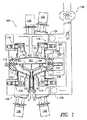
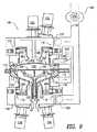
図1は、第1の実施形態の化学膜形成システム100で使用される熱反応チャンバ103の断面図を示している。チャンバ103は、CVDを含むがこれに制限されない適切な堆積プロセスなどの反応膜形成プロセスが遂行されるチャンバ103の内部容積を画成するチャンバ壁102を有している。ハウジング118がチャンバ壁102を包み、サポートしている。基板サポート構造104が、CVD処理中にチャンバ103内に基板106をサポートするために使用される。基板106は、膜が堆積または成長される上面を有しており、この上面は通常基板サポート構造104の外に面しているが、これは要件ではない。ゆえに、基板106の底面は通常基板サポート構造104に面して、これに接触している。 FIG. 1 shows a sectional view of a
処理中、ガスがエントリポート110を介してチャンバ103に入り、排出ポート112を介して除去される。処理中も、熱が赤外線放射バルブ114によって提供される。赤外線放射バルブ114は、ハウジング118に接続されているサポートアセンブリ116上に、チャンバ壁102に近接して搭載されている。チャンバ103のチャンバ壁102は透明であり、通常は石英からなり、また基板106を加熱するために、放射バルブ114からの赤外線放射が反応チャンバ103に自由に入れるようにする。チャンバ壁102は、基板106の上面に面している上部表面105と、基板106の底面および基板サポート構造104に面している底部表面107とを有している。 During processing, gas enters
熱反応器およびこの動作に関するより完全な説明が、「In−Situ Measurement Of A Thin Film Deposited On A Wafer」と題された、同一出願人による米国特許第5,258,824号と、「Double−dome Reactor for Semiconductor Processing」と題された米国特許第5,108,792号とに開示されており、これらの各々の内容全体は参照して本明細書に組み入れられる。処理中、チャンバ壁102は、実質的に透明であるが、依然として加熱される。チャンバ壁102を冷却するための冷却剤流が入口導管120を介してブロワ140からハウジング118に供給され、チャンバ壁102を越えて向けられ、出口導管122を介して排出される。より具体的には、冷却剤流は導管120を介して上部入口ポート124および下部入口ポート126を通ってハウジング118に供給される。冷却剤流は上部排出ポート128および下部排出ポート130を通ってハウジング118を出る。上部入口ポート124を通って入る冷却剤はチャンバ壁102の上部表面105を通過して、上部排出ポート128を通って出る。同様に、下部入口ポート126を通って入る冷却剤はチャンバ壁102の底部表面107を通過して、下部排出ポート130を通って出る。ハウジング118は、チャンバ壁102を越えて冷却剤を導くシュラウドを形成する。チャンバ壁102に沿った冷却剤のこの冷却剤流は反応チャンバ103のチャンバ壁102を冷却する。通常冷却剤は空気である。 A more complete description of the thermal reactor and its operation is described in commonly assigned US Pat. No. 5,258,824 entitled “In-Situ Measurement Of A Thin Film Deposed On A Wafer” and “Double- U.S. Pat. No. 5,108,792, entitled "Domes Reactor for Semiconductor Processing", the entire contents of each of which is incorporated herein by reference. During processing, the
チャンバ壁102の温度をコントロールするための代替的方法もまた、チャンバ壁102と接触している表面の水冷却や、窒素、ヘリウム、アルゴン、またはチャンバ壁102を流れる不活性ガスの使用を含むことがある。入口導管120に設置されている空気羽根や他の冷却剤流コントロールデバイスなどの冷却剤調節器131がハウジング118への冷却剤流の量をコントロールし、そしてチャンバ壁102の温度をコントロールする。代替的に、調整可能な虹彩、バルブ、ブロワ140用のブロワ速度コントロール回路などの、冷却剤流をコントロールするための他のデバイスが使用されてもよい。同時に、ブロワ140および冷却剤調節器131、または概説されているような他の適切な方法が、チャンバ壁102を冷却するための冷却システムを提供し、ここでは冷却システムによってチャンバ壁102に提供される冷却電力がコントロール可能である。つまりチャンバ壁102からの熱除去レートが、チャンバ壁102の温度をコントロールされた方法で調節するために、冷却システムによってコントロール可能である。 Alternative methods for controlling the temperature of the
チャンバ壁102の温度は、光学高温計、熱電対などの、当業界のものと類似の従来の温度測定デバイスを使用して監視されてもよい。例えば、チャンバ壁102の上部表面105の温度は光学高温計132を使用して監視されてもよく、光学高温計134は基板106の温度を測定するために使用されてもよく、光学高温計136は基板サポート構造104の温度を測定するために使用されてもよく、光学高温計138はチャンバ壁102の底部表面107の温度を監視するために使用されてもよい。 The temperature of the
上部表面105の測定温度を符号化する第1の信号が上部表面温度測定デバイス132から出力され、そして受信されてコントロール論理部200によって処理され、この実施形態は図2に表されている。同様に、底部表面107の測定温度を符号化する第2の信号が底部表面温度測定デバイス138から出力され、そして受信されてコントロール論理部200によって処理される。コントロール論理部200は、所定の温度軌道に従って処理期間にわたってチャンバ壁102の温度を変調するために、第1の信号、第2の信号またはこれら2つの関数を利用して冷却システムの冷却電力をコントロールする。 A first signal encoding the measured temperature of the
一実施形態では、コントロール論理部200は、メモリ220と電気連通しているプロセッサ210を備えている。メモリ220はコントロールコード221を備えており、これはプロセッサ210によって実行されて、かつプロセッサ210の動作をコントロールし、コントロールコード221はコントロール論理部200のオペレーティングシステムとして作用する。以下において、プロセッサ210がプログラムの1つを実行するとして説明される場合、プロセッサ210に上記のプログラムの1つを実行させるのはコントロールコード221である点が理解されるべきであり、コントロールコード221のプログラムを提供することは合理的に当業界の手段のうちであるべきである。 In one embodiment,
図2に開示されている実施形態では、プロセッサ210は、第1の信号を上部表面温度測定デバイス132から受信する上部表面温度入力231を介して上部表面105の温度を取得する。同様に、プロセッサ210は、第2の信号を底部表面温度測定デバイス138から受信する底部表面温度入力232を介して底部表面107の温度を取得する。コントロール論理部200は、プロセス期間のチャンバ壁102の温度を所定の方法で変調させることによって膜形成プロセスの動力学をコントロールするための独立パラメータを提供するために、特にチャンバ壁102を冷却するために使用される冷却システムをコントロールするために使用される。しかしながら、コントロール論理部200は、当業界で公知であるように、ガス流量、基板106および基板サポート構造104の温度を測定するための入力などの、図2に示されていない多数の更なる入力を含有してもよい点が明らかであるはずである。 In the embodiment disclosed in FIG. 2, the
コントロール論理部200は、プロセス関連情報をユーザーに供するためにディスプレイ238に、かつユーザーが情報をコントロール論理部200に入力できるようにするために入力デバイス239に提供されてもよい。プロセッサ210は、例えば上部表面105、底部表面107、基板106および基板サポート構造104の温度、現在のプロセスステップ、現在のプロセス時間、ガス流量などを供するためにディスプレイ238をコントロールすることができる。同様に、プロセッサ210は、入力デバイス239から受信されたデータに従ってメモリ220内に記憶されているパラメータを変更してもよく、このような変化は潜在的に、プロセッサ210によって実行されるプロセスステップへの変化をもたらし、ゆえにこのようなプロセッサ210の変化はCVDシステム100をコントロールすることになる。ディスプレイ238、入力デバイス239、コントロールコード221およびプロセッサ210は共に、当業と類似の方法でユーザー入力/出力(I/O)インタフェースを形成し、これによってユーザーは、CVDシステム100の監視およびコントロールの両方が可能になる。
示されている実施形態では、コントロール論理部200のメモリ220はまた、処理期間にわたってチャンバ壁102の少なくとも一部の温度をコントロールおよび変調するために使用される温度パラメータ222を含有している。温度パラメータ222は少なくとも1つのセットポイント223を備えており、通常は2つ以上のセットポイント223を有することになる。各セットポイント223はそれぞれの時間値224および温度値225を含有している。時間値224は処理期間内の時間を示しており、24時間、プロセス関連時間(つまり、プロセスの開始からの経過時間、またはこのプロセスの終了までの時間)、ステップ関連時間(つまり、プロセス内の現在のステップの開始からの経過時間、またはこのステップの終了までの時間)などの情報を符号化するのに適した任意のフォーマットであってもよい。温度値225は、セットポイント223の関連時間値224でのチャンバ壁102の温度変調部分に望ましい温度を示しており、このような温度情報を示すのに適した任意の形態であってもよく、例として摂氏またはケルビンのような絶対温度や、プロセス温度からのオフセットのような相対温度を含んでいる。 In the illustrated embodiment, the
同時に、セットポイント223は、処理期間にわたってチャンバ壁102の温度変調部分の温度軌道情報を提供する。処理期間中の所定の間隔、例えば0.01秒間隔で、コントロール論理部200はチャンバ壁102の温度情報を温度入力231、232から取得し、この情報を利用して、現在の測定温度229を生成する。温度入力231、232などのうちの1つのみを使用する平均化、重み平均化などによる任意の方法が、現在の測定温度229を生成するために使用されてもよい。これはユーザーI/Oインタフェースを介してユーザーによって選択可能である。プロセッサ210は次いで(タイマ240から取得されるような)現在の時間および時間値224を使用して、温度パラメータ情報222にインデックス化して、現在の時刻がある最近のセットポイント223を見つける。 At the same time, the
依然として図2を参照すると、次に、プロセッサ210は、最近のセットポイント223の関連温度値225を使用して、チャンバ壁102の温度変調部分の現在の目標温度228を決定するための線形補間(または他の適切な補間)を実行する。通常2つのセットポイント223(または、最小の時間値224の前および最大の時間値224より大きければ1つのセットポイント)が最近のセットポイント223として使用されるが、実行される補間の種類に応じて3つ以上使用されてもよい。プロセッサ210は現在の測定温度229および現在の目標温度228を標準フィードバックループへの入力として利用して、現在の測定温度229が現在の目標温度228に達するように、チャンバ壁102の温度変調部分に対する冷却システムの電力レベルをコントロールする。連続フィードバックによって、時間の関数としての現在の測定温度229は、冷却システムの測定誤差および機械的制限内で、温度パラメータ222を実質的に追跡するはずである。 Still referring to FIG. 2, the
図1および図2に描かれている実施形態では、例えばプロセッサ210は信号を冷却電力コントロール出力233に送り、測定温度229および目標温度228に基づいて冷却剤調節器131をコントロールする。現在の測定温度229と現在の目標温度228の差が正である(つまり、チャンバ壁102の温度変調部分が所望するよりも現在のところ熱い)場合、プロセッサ210は冷却電力コントロール出力233に信号を送り、冷却剤調節器131をさらに開いて、チャンバ壁102に流れる冷却剤のレートを増大させる。つまり冷却システムの冷却電力を増大させる。反対に、差が負の場合、プロセッサ210は、冷却システムの冷却電力を減少させるために、冷却剤調節器131に冷却剤の流れをさらに制約するように命令する。プロセッサ210は、冷却剤調節器131は空気流をどの程度制約または許容するか、つまりどの程度冷却電力が増減されるかを決定するために、現在の測定温度229および目標温度228の差の大きさを利用してもよい。 In the embodiment depicted in FIGS. 1 and 2, for example, the
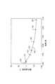
例証として、図3は、処理期間の一部でのチャンバ壁102の平均温度の仮定的な所望の温度軌道を図示している。図3のグラフは、膜形成ステップの開始温度であってもよい事前定義されたプロセス温度に対する温度差を示すために正規化される。ユーザーは、チャンバ壁102が事前焼成ステップからプロセス温度に冷却し、プロセス温度で安定するのに約10秒かかり、そして膜形成ステップの開始時に、膜形成ステップの完了時にプロセス温度未満の約65℃である温度に至る漸近的傾斜を開始することを所望することがある。膜形成ステップでのチャンバ壁102のこの定常的に減少する温度はファセット化を低減する助けとなる。ユーザーは漸近曲線260を近似するために6個のポイント252〜257を、膜形成ステップ前に10秒の温度安定期間を提供するために2個のポイント251、252を使用することを決定してもよい。 As an illustration, FIG. 3 illustrates a hypothetical desired temperature trajectory of the average temperature of the
膜形成ステップが1340秒のプロセス時間で開始する場合、コントロール論理部200のI/Oシステムは、温度パラメータ222の7個の対応するセットポイント223を入力するように利用されてもよい。第1のセットポイント223は第1のポイント251で1330の時間224および0℃の温度225を有しており、第2のセットポイント223は第2のポイント252で1340の時間224および0℃の温度225を有しており、第3のセットポイント223は第3のポイント253で1370の時間224および−25℃の温度225を有しており、第4のセットポイント223は第4のポイント254で1405の時間224および−35℃の温度225を有しており、第5のセットポイント223は第5のポイント255で1440の時間224および−45℃の温度225を有しており、第6のセットポイント223は第6のポイント256で1510の時間224および−60℃の温度225を有しており、最後に第7のセットポイント223は第7のポイント257で1560の時間224および−65℃の温度225を有している。I/Oシステムはそして、上部表面温度入力231および底部表面温度入力232から取得された平均値を使用して現在の測定温度229を生成することをコントロール論理部200に命令するために利用されてもよい。膜形成プロセス中、コントロール論理部200は次いで、温度パラメータ222の7個のセットポイント223を使用して冷却剤調節器131をコントロールすることによって、現在の測定温度229が現在の目標温度228を追跡する。当然、この場合の目標温度228は実際の温度ではなく、事前定義されたプロセス温度に基づいた温度差である点が明らかである。つまり、現在の測定温度229を生成する場合、コントロール論理部200は公知の一定のプロセス温度を減算して、現在の測定温度229の温度差を生み出すことがある。例えば、1470のプロセス時間では、図3に示されているように、コントロール論理部200は第5のポイント255および第6のポイント256の第5および第6のセットポイント223を外挿して、プロセス温度未満の53℃の現在の目標温度228を見つける。コントロール論理部200は、その後、−53℃の現在の目標温度228および現在の測定温度229の値に基づいて信号を冷却電力コントロール出力233に送り、冷却システムを調節することによって、チャンバ壁102の平均温度はセットポイント223によって定義された温度軌道を追跡する。冷却剤調節器131はまた、チャンバ壁102の温度軌道をコントロールするように手動で調整されてもよい。 If the film formation step begins with a process time of 1340 seconds, the I / O system of
上記例示的実施形態では、セットポイント223は温度値225を利用して、処理期間にわたるチャンバ壁102の変調表面の所望の温度軌道を定義する温度パラメータ222を構築する。しかしながら、図4を参照すると、冷却システムの電力(つまり、ブロワ140の速度および/または冷却剤調節器131の設定)および加熱要素114の放射輝度の密接な相関があるため、別の実施形態としては、各々が関連時間値324および冷却電力レベル値325を有する1つ以上のセットポイント323を有しているものとして温度パラメータ322を定義することが等しく可能である。この場合、第2の実施形態のコントロール論理部300のプロセッサ310は、現在の目標温度228を見つけるために上記で使用されたのと同様に現在の目標冷却電力レベル328を生成してから、信号を冷却電力コントロール出力333に送り、冷却システム(つまり、ブロワ140および/または冷却剤調節器131)の電力を設定して、現在の目標冷却電力レベル328に一致させる。 In the exemplary embodiment,
実行されている処理の固有の一貫性および再現性ゆえに、それぞれの時間値324で一連の冷却電力レベル325として定義されている温度パラメータ322は、上記実施形態の温度パラメータ222と機能的に類似している。しかしながら、チャンバ壁102の変調領域の所望の温度と実際の温度のばらつきは、第1の実施形態より大きいこともある。 Due to the inherent consistency and repeatability of the process being performed, the
本発明の実施形態は、処理期間でのチャンバ壁102の全体またはチャンバ壁102の一部の変調コントロールを提供する。特に、図3に示されているように、膜形成プロセスの個々のステップでのチャンバ壁102の変調コントロールが達成可能である。例えば、ファセット化が低減されたより高い全成長速度が、基板上での膜の堆積や成長が進むに伴って上部表面105の温度をまず増大させてから、上部表面105の温度をゆっくりと減少させる温度パラメータ222、322を提供することによって達成可能である。温度パラメータ222、322の選択は、最適化される特性に左右される。例えば、壁102の温度の増大によってガスはより良好に分裂(crack)または分解することによって、成長速度を高めることができる。一部のドーパント種は、分解される場合により良好に吸収または一体化するため、膜組成はこの機構によっても変化することがある。このすべては、膜形成手順が種々の段階を経るに伴って、プロセスステップ内で行われてもよい。従って、当業者は、所望の膜特性を達成するために温度パラメータ222、322を実験的に決定および選択可能である点が理解される。 Embodiments of the present invention provide modulation control of the
図5および図6を参照すると、第3の実施形態のシステム400が、チャンバ壁102の複数の部分の温度の独立コントロールを可能にすることによって、膜堆積プロセスの更なる独立パラメータを提供する。提示を容易にするために、従来の実施形態と本質的に同一の図5のコンポーネントには同一の参照番号が提供されてきた。図1の記述に示されているように、入口ポート124に入る冷却剤はチャンバ壁102の上部表面105を通過することによって上部表面105を冷却する。同様に、底部入口ポート126に入る冷却剤は底部表面107を冷却する。ゆえに、上部入口ポート124および底部入口ポート126に入る冷却剤の量を独立してコントロールすることによって、チャンバ壁102の上部表面105および底部表面107の温度をそれぞれ独立してコントロールすることが可能である。これを達成するために、本実施形態は、上部入口ポート124への冷却剤流量をコントロールするための第1の冷却剤調節器431と、下部入口ポート126への冷却剤流量をコントロールするための第2の冷却剤調節器439とを提供する。 With reference to FIGS. 5 and 6, the
冷却剤調節器431、439は空気羽根、調整可能な虹彩、バルブ、それぞれのチャンバ壁102の表面と接触している液体冷却表面などであってもよい。代替的に、冷却剤調節器431、439のうちの一方は空気羽根、調整可能な虹彩、バルブ、冷却表面などであってもよく、他方はブロワ140の速度をコントロールするためのブロワ速度コントロール回路を利用するものであってもよい。 The
図5に示されている実施形態のコントロール論理部500は先行の実施形態のものと類似しているが、それぞれメモリ520に記憶されている第1の温度パラメータ560および第2の温度パラメータ570に従った第1の冷却剤調節器431および第2の冷却剤調節器439の独立コントロールを提供する。第1の温度パラメータ560は処理期間での上部表面105の所望の温度軌道を定義する。第2の温度パラメータ570は、処理期間での底部表面107の所望の温度軌道を定義する。例えば、図7を参照すると、第1の温度パラメータ560は、プロセス温度に対する上部表面105に対して、図3に描かれているのと類似の第1の温度軌道601を定義する15個のセットポイント563を有することがある。例えば、7個のポイント611〜617は、上部表面105の事前焼成温度軌道610を備えてもよい。4個のポイント621〜624は、膜堆積ステップ中に増大する上部表面105の膜堆積温度軌道620を備えてもよい。この増大は、膜堆積ステップの期間にわたってプロセス温度からより高い目標温度へと実質的に漸近的であってもよい。膜堆積ステップ中の上部表面105の温度のこのような増大はより高い堆積レートを生じさせる。4個のポイント631〜634は、上部表面105の冷却温度軌道630を備えてもよい。 The
第2の温度パラメータ570もまた、例えば、膜形成プロセス全体で底部表面107の第2の温度軌道602を定義する8個のセットポイント573を有してもよい。プロセッサ510は、第1の現在の目標温度523を生成するために第1の温度パラメータ560を利用してもよく、また第2の現在の目標温度524を生成するために第2の温度パラメータ570を利用してもよい。上部表面温度測定デバイス132から第1の信号を受信する上部表面温度入力531などの入力の監視によって、プロセッサ510は現在の上部表面温度521を生成することができる。同様に、底部表面温度測定デバイス138から第2の信号を受信する底部表面温度入力532を監視することによって、プロセッサ510は現在の底部表面温度522を生成してもよい。当然、現在の上部表面温度521ならびに現在の底部表面温度522は、ユーザーによって所望されるような複数の入力の関数であってもよい。 The
先行の実施形態と同様に、プロセッサ510は第1の現在の目標温度523および現在の上部表面温度521を利用して、信号を第1の冷却電力コントロール出力533に送って、第1の冷却剤調節器431をコントロールすることによって、第1の温度パラメータ560に従って上部表面105の温度を変調する。同様に、プロセッサ510は第2の現在の目標温度524および現在の底部表面温度522を利用して、信号を第2の冷却電力コントロール出力534に送って第2の冷却剤調節器439をコントロールすることによって、第1の温度パラメータ560に従って底部表面107の温度を変調する。当然、第1の温度パラメータ560および第2の温度パラメータ570は、第2の実施形態で行われたように、温度ではなくそれぞれの冷却電力レベルによって定義されてもよく、この場合、現在の上部表面温度521または現在の底部表面温度522を監視して、第1の冷却剤調節器431および第2の冷却剤調節器439をコントロールする必要がない。 Similar to the previous embodiment, the
図8に示されているように、第1の変速ブロワ701および第2の変速ブロワ702を使用して、チャンバ壁102の上部表面105および底部表面107の温度をそれぞれコントロールすることができる。図6をさらに参照すると、コントロール論理部500は、図8に描かれている実施形態をコントロールするのに等しく適している。第1の冷却電力コントロール出力533は第1のブロワ701の速度をコントロール可能であるのに対して、第2の冷却電力コントロール出力534は第2のブロワ702の速度をコントロール可能である。 As shown in FIG. 8, a
図9を参照すると、上部ランプ802と底部ランプ804間の照射(irradiancy)バイアスを変更することによって上部表面105および底部表面107の温度を独立してコントロールすることができる。上部ランプ802はチャンバ壁102の上部表面105の上方に配置されているため、基板106を加熱しつつ上部表面105を加熱する。底部ランプ804はチャンバ壁102の底部表面107の下方に配置されているため、基板106を加熱しつつ底部表面107を加熱する。上部ランプ802および底部ランプ804の結合照射は、基板106の最終温度を決定する。上部ランプ802の照射が増大される一方で、底部ランプ804の照射が減少される場合、基板106を同一温度に保ちつつ、上部表面105の温度を増大させ、かつ底部表面107の温度を減少させることができる。これと反対に、照射バイアスは、基板106の温度を維持しつつ底部表面107の加熱および上部表面105の冷却をもたらす。上部ランプ802の照射は従って、底部ランプ804の照射と無関係にコントロール可能である。図6を参照すると、上部ランプ802および底部ランプ804の独立コントロールによってコントロール回路500は、上部ランプ802と底部ランプ804間の照射バイアスをコントロールできるようになる。第1の冷却電力コントロール出力533は従って、変速ブロワ140の速度をコントロールするために使用されてもよいのに対して、第2の冷却電力コントロール出力534は、上部ランプ802と底部ランプ804間の照射バイアスをコントロールするために使用されてもよい。第2の冷却電力コントロール出力534は実際に、上部ランプ802および底部ランプ804の照射をそれぞれコントロールする2つの独立出力であってもよく、またこれら2つの照射出力の差は、一方の表面107、105に対してもう一方の表面105、107のうちの一方を優先的に加熱および冷却する照射バイアスを生じさせることが認識される。 Referring to FIG. 9, the temperature of the
例えば、底部表面107を冷却するために、プロセッサ510は第2の冷却電力コントロール出力534をコントロール可能であるため、上部ランプ802の照射は増大するのに対して、底部ランプ804の照射は減少する。基板106の温度概観からはほとんど変更がなかった。しかしながら、底部表面107の観点から、底部表面107に少ない放射エネルギーが作用すると、底部表面107は冷却を開始する。より多くの放射エネルギーが上部表面105に作用するため、上部表面105はこの第1の温度パラメータ560を超えて加熱を開始することがある点が認識される。これに応答して、プロセッサ510は、変速ブロワ140の速度を増大させて上部表面105を冷却するために第1の冷却電力コントロール出力533をコントロールしてもよく、これは底部表面107の更なる冷却を付随的にもたらす。同様に、バイアスを逆にすることによって、底部表面107の加熱をもたらすことができる。ゆえに、第2の冷却電力コントロール出力534を使用してランプ802、804間の照射バイアスを変調することによって、プロセッサは、上部表面105に対して底部表面107の温度を選択的に昇降させることができる。 For example, to cool the
チャンバ壁102の上部および底部表面105、107を温度変調するだけでなく、チャンバ壁102の側面部分を変調することも可能である。例えば、図1を参照すると、入口および出口のダクトの適切なコントロールによって、左に隣接する上部表面151および右に隣接する上部表面152のそれぞれの温度をコントロールすることができる。隣接する上部表面151、152は上部表面105に隣接しているため、基板106の上部表面に隣接することになる。同様に、左に隣接する底部表面153および右に隣接する底部表面154を温度変調することが可能であり、これらは底部表面107に隣接しているため、基板106の底部表面に隣接することになる。コントロール論理部は、温度変調する個々のチャンバ壁表面部分と同数の温度パラメータを受容するように容易に拡張可能であり、これを実行する方法は本開示に照らして明確であるはずである。 In addition to temperature modulating the top and
本発明はここで特定の実施形態を参照して説明されてきたが、これらの実施形態は本発明の原理および用途の例示に過ぎないことが理解されるべきである。種々の修正および変形が、本発明の精神および範囲から逸脱することなく本発明の方法になされてもよいことは当業者に明らかである。従って、本発明は、添付の請求項およびこれらの同等物の範囲内の修正および変形を含むことが意図されている。 Although the invention herein has been described with reference to particular embodiments, it is to be understood that these embodiments are merely illustrative of the principles and applications of the present invention. It will be apparent to those skilled in the art that various modifications and variations can be made to the method of the present invention without departing from the spirit and scope of the invention. Thus, it is intended that the present invention include modifications and variations that are within the scope of the appended claims and their equivalents.
100…膜形成システム、102…チャンバ壁、103…熱反応チャンバ、104…基板サポート構造、105…上部表面、106…基板、107…底部表面、110…エントリポート、112…排出ポート、114…赤外線放射バルブ、116…サポートアセンブリ、118…ハウジング、120…入口導管、122…出口導管、124…上部入口ポート、126…下部入口ポート、128…上部排出ポート、130…下部排出ポート、131…冷却剤調節器、132、134、136、138…光学高温計、140ブロワ、151…左に隣接する上部表面、152…右に隣接する上部表面、153…左に隣接する底部表面、154…右に隣接する底部表面、200…コントロール論理部、210…プロセッサ、221…コントロールコード、220…メモリ、223…セットポイント、224…時間値、225…温度値、228…現在の目標温度、229…現在の測定温度、231、232…温度入力、233…冷却電力コントロール出力、238…ディスプレイ、239…入力デバイス、240…タイマ、251、252、253、254、255、256、257…ポイント、260…漸近曲線、300…コントロール論理部、322…温度パラメータ、323…セットポイント、324…時間値、325…冷却電力レベル値、328…現在の目標冷却電力レベル、333…冷却電力コントロール出力、400…コントロール論理部、431、439…冷却剤調節器、500…コントロール論理部、510…プロセッサ、520…メモリ、521…現在の上部表面温度、522…現在の底部表面温度、523…第1の現在の目標温度、524…第2の現在の目標温度、531…上部表面温度入力、532…底部表面温度入力、533…冷却電力コントロール出力、560…第1の温度パラメータ、570…第2の温度パラメータ、701…第1の変速ブロワ、702…第2の変速ブロワ、802…上部ランプ、804…底部ランプDESCRIPTION OF
Claims (28)
Translated fromJapanese膜形成プロセスを実行するために複数の壁によって囲まれている反応チャンバに基板を置くステップと、
前記膜形成プロセス中に少なくとも第1の壁の温度を不定値で変調するステップと、
を備える方法。A method for forming a film on a substrate, comprising:
Placing the substrate in a reaction chamber surrounded by a plurality of walls to perform a film formation process;
Modulating the temperature of at least the first wall with an indefinite value during the film formation process;
A method comprising:
第1の温度パラメータを選択するステップであって、前記第1の温度パラメータが処理期間中不定値であるステップと、
前記基板を処理チャンバのチャンバ壁内に配置するステップと、
前記処理期間中に前記基板上に前記膜を形成するステップと、
前記チャンバ壁の第1の部分の温度が第1の温度パラメータに実質的に準拠するように、前記処理期間中に前記チャンバ壁の前記第1の部分の前記温度をコントロールするステップと、
を備える方法。A method for forming a film on a substrate, comprising:
Selecting a first temperature parameter, wherein the first temperature parameter is an indefinite value during the processing period;
Placing the substrate in a chamber wall of a processing chamber;
Forming the film on the substrate during the processing period;
Controlling the temperature of the first portion of the chamber wall during the processing period such that the temperature of the first portion of the chamber wall substantially conforms to a first temperature parameter;
A method comprising:
前記チャンバ壁の第2の部分の温度が前記処理期間中に前記第2の温度パラメータに実質的に準拠するように、前記チャンバ壁の前記第2の部分の前記温度をコントロールするステップと、
をさらに備える、請求項7に記載の方法。Selecting a second temperature parameter, wherein the second temperature parameter is an indefinite value over the processing period;
Controlling the temperature of the second portion of the chamber wall such that the temperature of the second portion of the chamber wall substantially conforms to the second temperature parameter during the processing period;
The method of claim 7, further comprising:
前記チャンバ壁の第1の部分を冷却するための第1の冷却システムと、
前記第1の冷却システムの冷却電力をコントロールするための第1の調節器と、
前記第1の調節器をコントロールするためのコントロール論理部であって、処理期間にわたる前記チャンバ壁の前記第1の部分の所望の温度軌道を定義する第1の温度パラメータを保持するメモリと、前記第1の温度パラメータを入力するためのユーザー入力/出力システムと、前記第1の調節器をコントロールするための第1の出力と、前記第1の温度パラメータに従って前記処理期間にわたって前記第1の出力に第1の信号を送るための処理回路とを備えるコントロール論理部と、
を備える膜形成システム。A chamber wall adapted to receive a substrate on which a film is formed;
A first cooling system for cooling the first portion of the chamber wall;
A first regulator for controlling the cooling power of the first cooling system;
Control logic for controlling the first regulator, the memory holding a first temperature parameter defining a desired temperature trajectory of the first portion of the chamber wall over a processing period; A user input / output system for inputting a first temperature parameter, a first output for controlling the first regulator, and the first output over the processing period according to the first temperature parameter A control logic comprising a processing circuit for sending a first signal to
A film forming system comprising:
前記第2の冷却システムの前記冷却電力をコントロールするための第2の調節器とをさらに備えており、
前記コントロール論理部がさらに前記第2の調節器をコントロールするための第2の出力を備えており、前記処理回路が、前記メモリに記憶されている第2の温度パラメータに従って前記処理期間中に第2の信号を前記第2の出力に送ることができる、請求項22に記載のシステム。A second cooling system for cooling the second portion of the chamber wall;
A second regulator for controlling the cooling power of the second cooling system;
The control logic further comprises a second output for controlling the second regulator, and the processing circuit is configured to output a second value during the processing period according to a second temperature parameter stored in the memory. 23. The system of claim 22, wherein two signals can be sent to the second output.
Applications Claiming Priority (3)
| Application Number | Priority Date | Filing Date | Title |
|---|---|---|---|
| US11/205,647US7718225B2 (en) | 2005-08-17 | 2005-08-17 | Method to control semiconductor film deposition characteristics |
| US11/205,647 | 2005-08-17 | ||
| PCT/US2006/030913WO2007021692A2 (en) | 2005-08-17 | 2006-08-08 | Method and apparatus to control semiconductor film deposition characteristics |
Publications (3)
| Publication Number | Publication Date |
|---|---|
| JP2009507997Atrue JP2009507997A (en) | 2009-02-26 |
| JP2009507997A5 JP2009507997A5 (en) | 2009-08-13 |
| JP5329221B2 JP5329221B2 (en) | 2013-10-30 |
Family
ID=37758095
Family Applications (1)
| Application Number | Title | Priority Date | Filing Date |
|---|---|---|---|
| JP2008526993AActiveJP5329221B2 (en) | 2005-08-17 | 2006-08-08 | Method and apparatus for controlling semiconductor film deposition characteristics |
Country Status (5)
| Country | Link |
|---|---|
| US (2) | US7718225B2 (en) |
| JP (1) | JP5329221B2 (en) |
| KR (2) | KR101014907B1 (en) |
| TW (1) | TWI358754B (en) |
| WO (1) | WO2007021692A2 (en) |
Cited By (1)
| Publication number | Priority date | Publication date | Assignee | Title |
|---|---|---|---|---|
| JP2018511181A (en)* | 2015-03-27 | 2018-04-19 | アプライド マテリアルズ インコーポレイテッドApplied Materials,Incorporated | Closed loop control of upper dome temperature |
Families Citing this family (419)
| Publication number | Priority date | Publication date | Assignee | Title |
|---|---|---|---|---|
| US7718225B2 (en)* | 2005-08-17 | 2010-05-18 | Applied Materials, Inc. | Method to control semiconductor film deposition characteristics |
| US8986456B2 (en)* | 2006-10-10 | 2015-03-24 | Asm America, Inc. | Precursor delivery system |
| US8706314B2 (en)* | 2008-07-31 | 2014-04-22 | Oracle America, Inc. | Method and apparatus for regulating temperature in a computer system |
| US10378106B2 (en) | 2008-11-14 | 2019-08-13 | Asm Ip Holding B.V. | Method of forming insulation film by modified PEALD |
| US9394608B2 (en) | 2009-04-06 | 2016-07-19 | Asm America, Inc. | Semiconductor processing reactor and components thereof |
| US20100263588A1 (en)* | 2009-04-15 | 2010-10-21 | Gan Zhiyin | Methods and apparatus for epitaxial growth of semiconductor materials |
| US8877655B2 (en) | 2010-05-07 | 2014-11-04 | Asm America, Inc. | Systems and methods for thin-film deposition of metal oxides using excited nitrogen-oxygen species |
| US8802201B2 (en) | 2009-08-14 | 2014-08-12 | Asm America, Inc. | Systems and methods for thin-film deposition of metal oxides using excited nitrogen-oxygen species |
| US8883270B2 (en)* | 2009-08-14 | 2014-11-11 | Asm America, Inc. | Systems and methods for thin-film deposition of metal oxides using excited nitrogen—oxygen species |
| US9312155B2 (en) | 2011-06-06 | 2016-04-12 | Asm Japan K.K. | High-throughput semiconductor-processing apparatus equipped with multiple dual-chamber modules |
| US9793148B2 (en) | 2011-06-22 | 2017-10-17 | Asm Japan K.K. | Method for positioning wafers in multiple wafer transport |
| US10364496B2 (en) | 2011-06-27 | 2019-07-30 | Asm Ip Holding B.V. | Dual section module having shared and unshared mass flow controllers |
| US10854498B2 (en) | 2011-07-15 | 2020-12-01 | Asm Ip Holding B.V. | Wafer-supporting device and method for producing same |
| US20130023129A1 (en) | 2011-07-20 | 2013-01-24 | Asm America, Inc. | Pressure transmitter for a semiconductor processing environment |
| DE102011083245B4 (en)* | 2011-09-22 | 2019-04-25 | Siltronic Ag | Method and device for depositing an epitaxial layer of silicon on a semiconductor wafer of monocrystalline silicon by vapor deposition in a process chamber |
| US9096931B2 (en) | 2011-10-27 | 2015-08-04 | Asm America, Inc | Deposition valve assembly and method of heating the same |
| US9341296B2 (en) | 2011-10-27 | 2016-05-17 | Asm America, Inc. | Heater jacket for a fluid line |
| US9017481B1 (en) | 2011-10-28 | 2015-04-28 | Asm America, Inc. | Process feed management for semiconductor substrate processing |
| US9167625B2 (en) | 2011-11-23 | 2015-10-20 | Asm Ip Holding B.V. | Radiation shielding for a substrate holder |
| US9005539B2 (en) | 2011-11-23 | 2015-04-14 | Asm Ip Holding B.V. | Chamber sealing member |
| US9202727B2 (en) | 2012-03-02 | 2015-12-01 | ASM IP Holding | Susceptor heater shim |
| US8946830B2 (en) | 2012-04-04 | 2015-02-03 | Asm Ip Holdings B.V. | Metal oxide protective layer for a semiconductor device |
| TWI622664B (en) | 2012-05-02 | 2018-05-01 | Asm智慧財產控股公司 | Phase stable film, structure and device comprising the same, and method of forming same |
| US8728832B2 (en) | 2012-05-07 | 2014-05-20 | Asm Ip Holdings B.V. | Semiconductor device dielectric interface layer |
| US8933375B2 (en) | 2012-06-27 | 2015-01-13 | Asm Ip Holding B.V. | Susceptor heater and method of heating a substrate |
| US9558931B2 (en) | 2012-07-27 | 2017-01-31 | Asm Ip Holding B.V. | System and method for gas-phase sulfur passivation of a semiconductor surface |
| US9117866B2 (en) | 2012-07-31 | 2015-08-25 | Asm Ip Holding B.V. | Apparatus and method for calculating a wafer position in a processing chamber under process conditions |
| US9169975B2 (en) | 2012-08-28 | 2015-10-27 | Asm Ip Holding B.V. | Systems and methods for mass flow controller verification |
| US9659799B2 (en) | 2012-08-28 | 2017-05-23 | Asm Ip Holding B.V. | Systems and methods for dynamic semiconductor process scheduling |
| US9021985B2 (en) | 2012-09-12 | 2015-05-05 | Asm Ip Holdings B.V. | Process gas management for an inductively-coupled plasma deposition reactor |
| US9324811B2 (en) | 2012-09-26 | 2016-04-26 | Asm Ip Holding B.V. | Structures and devices including a tensile-stressed silicon arsenic layer and methods of forming same |
| US10714315B2 (en) | 2012-10-12 | 2020-07-14 | Asm Ip Holdings B.V. | Semiconductor reaction chamber showerhead |
| US9640416B2 (en) | 2012-12-26 | 2017-05-02 | Asm Ip Holding B.V. | Single-and dual-chamber module-attachable wafer-handling chamber |
| US8772055B1 (en) | 2013-01-16 | 2014-07-08 | Applied Materials, Inc. | Multizone control of lamps in a conical lamphead using pyrometers |
| US8894870B2 (en) | 2013-02-01 | 2014-11-25 | Asm Ip Holding B.V. | Multi-step method and apparatus for etching compounds containing a metal |
| US20160376700A1 (en) | 2013-02-01 | 2016-12-29 | Asm Ip Holding B.V. | System for treatment of deposition reactor |
| US9748121B2 (en)* | 2013-03-05 | 2017-08-29 | Applied Materials, Inc. | Thermal coupled quartz dome heat sink |
| US9484191B2 (en) | 2013-03-08 | 2016-11-01 | Asm Ip Holding B.V. | Pulsed remote plasma method and system |
| US9589770B2 (en) | 2013-03-08 | 2017-03-07 | Asm Ip Holding B.V. | Method and systems for in-situ formation of intermediate reactive species |
| US8993054B2 (en) | 2013-07-12 | 2015-03-31 | Asm Ip Holding B.V. | Method and system to reduce outgassing in a reaction chamber |
| US9018111B2 (en) | 2013-07-22 | 2015-04-28 | Asm Ip Holding B.V. | Semiconductor reaction chamber with plasma capabilities |
| US9396934B2 (en) | 2013-08-14 | 2016-07-19 | Asm Ip Holding B.V. | Methods of forming films including germanium tin and structures and devices including the films |
| US9793115B2 (en) | 2013-08-14 | 2017-10-17 | Asm Ip Holding B.V. | Structures and devices including germanium-tin films and methods of forming same |
| US9240412B2 (en) | 2013-09-27 | 2016-01-19 | Asm Ip Holding B.V. | Semiconductor structure and device and methods of forming same using selective epitaxial process |
| US9556516B2 (en) | 2013-10-09 | 2017-01-31 | ASM IP Holding B.V | Method for forming Ti-containing film by PEALD using TDMAT or TDEAT |
| US9605343B2 (en) | 2013-11-13 | 2017-03-28 | Asm Ip Holding B.V. | Method for forming conformal carbon films, structures conformal carbon film, and system of forming same |
| US10179947B2 (en) | 2013-11-26 | 2019-01-15 | Asm Ip Holding B.V. | Method for forming conformal nitrided, oxidized, or carbonized dielectric film by atomic layer deposition |
| US9338834B2 (en) | 2014-01-17 | 2016-05-10 | Taiwan Semiconductor Manufacturing Company Limited | Systems and methods for microwave-radiation annealing |
| US10683571B2 (en) | 2014-02-25 | 2020-06-16 | Asm Ip Holding B.V. | Gas supply manifold and method of supplying gases to chamber using same |
| US10167557B2 (en) | 2014-03-18 | 2019-01-01 | Asm Ip Holding B.V. | Gas distribution system, reactor including the system, and methods of using the same |
| US9447498B2 (en) | 2014-03-18 | 2016-09-20 | Asm Ip Holding B.V. | Method for performing uniform processing in gas system-sharing multiple reaction chambers |
| US11015245B2 (en) | 2014-03-19 | 2021-05-25 | Asm Ip Holding B.V. | Gas-phase reactor and system having exhaust plenum and components thereof |
| US9404587B2 (en) | 2014-04-24 | 2016-08-02 | ASM IP Holding B.V | Lockout tagout for semiconductor vacuum valve |
| US10858737B2 (en) | 2014-07-28 | 2020-12-08 | Asm Ip Holding B.V. | Showerhead assembly and components thereof |
| US9543180B2 (en) | 2014-08-01 | 2017-01-10 | Asm Ip Holding B.V. | Apparatus and method for transporting wafers between wafer carrier and process tool under vacuum |
| US9890456B2 (en) | 2014-08-21 | 2018-02-13 | Asm Ip Holding B.V. | Method and system for in situ formation of gas-phase compounds |
| US9657845B2 (en) | 2014-10-07 | 2017-05-23 | Asm Ip Holding B.V. | Variable conductance gas distribution apparatus and method |
| US10941490B2 (en) | 2014-10-07 | 2021-03-09 | Asm Ip Holding B.V. | Multiple temperature range susceptor, assembly, reactor and system including the susceptor, and methods of using the same |
| US10095114B2 (en) | 2014-11-14 | 2018-10-09 | Applied Materials, Inc. | Process chamber for field guided exposure and method for implementing the process chamber |
| KR102300403B1 (en) | 2014-11-19 | 2021-09-09 | 에이에스엠 아이피 홀딩 비.브이. | Method of depositing thin film |
| KR102263121B1 (en) | 2014-12-22 | 2021-06-09 | 에이에스엠 아이피 홀딩 비.브이. | Semiconductor device and manufacuring method thereof |
| US9478415B2 (en) | 2015-02-13 | 2016-10-25 | Asm Ip Holding B.V. | Method for forming film having low resistance and shallow junction depth |
| US10529542B2 (en) | 2015-03-11 | 2020-01-07 | Asm Ip Holdings B.V. | Cross-flow reactor and method |
| US10276355B2 (en) | 2015-03-12 | 2019-04-30 | Asm Ip Holding B.V. | Multi-zone reactor, system including the reactor, and method of using the same |
| US9864276B2 (en) | 2015-04-07 | 2018-01-09 | Applied Materials, Inc. | Laser annealing and electric field |
| US10458018B2 (en) | 2015-06-26 | 2019-10-29 | Asm Ip Holding B.V. | Structures including metal carbide material, devices including the structures, and methods of forming same |
| US10600673B2 (en) | 2015-07-07 | 2020-03-24 | Asm Ip Holding B.V. | Magnetic susceptor to baseplate seal |
| US10043661B2 (en) | 2015-07-13 | 2018-08-07 | Asm Ip Holding B.V. | Method for protecting layer by forming hydrocarbon-based extremely thin film |
| US9899291B2 (en) | 2015-07-13 | 2018-02-20 | Asm Ip Holding B.V. | Method for protecting layer by forming hydrocarbon-based extremely thin film |
| US10083836B2 (en) | 2015-07-24 | 2018-09-25 | Asm Ip Holding B.V. | Formation of boron-doped titanium metal films with high work function |
| US10087525B2 (en) | 2015-08-04 | 2018-10-02 | Asm Ip Holding B.V. | Variable gap hard stop design |
| US9647114B2 (en) | 2015-08-14 | 2017-05-09 | Asm Ip Holding B.V. | Methods of forming highly p-type doped germanium tin films and structures and devices including the films |
| US9711345B2 (en) | 2015-08-25 | 2017-07-18 | Asm Ip Holding B.V. | Method for forming aluminum nitride-based film by PEALD |
| US9960072B2 (en) | 2015-09-29 | 2018-05-01 | Asm Ip Holding B.V. | Variable adjustment for precise matching of multiple chamber cavity housings |
| US9909214B2 (en) | 2015-10-15 | 2018-03-06 | Asm Ip Holding B.V. | Method for depositing dielectric film in trenches by PEALD |
| US10211308B2 (en) | 2015-10-21 | 2019-02-19 | Asm Ip Holding B.V. | NbMC layers |
| US10322384B2 (en) | 2015-11-09 | 2019-06-18 | Asm Ip Holding B.V. | Counter flow mixer for process chamber |
| US9455138B1 (en) | 2015-11-10 | 2016-09-27 | Asm Ip Holding B.V. | Method for forming dielectric film in trenches by PEALD using H-containing gas |
| US9905420B2 (en) | 2015-12-01 | 2018-02-27 | Asm Ip Holding B.V. | Methods of forming silicon germanium tin films and structures and devices including the films |
| US9607837B1 (en) | 2015-12-21 | 2017-03-28 | Asm Ip Holding B.V. | Method for forming silicon oxide cap layer for solid state diffusion process |
| US9627221B1 (en) | 2015-12-28 | 2017-04-18 | Asm Ip Holding B.V. | Continuous process incorporating atomic layer etching |
| US9735024B2 (en) | 2015-12-28 | 2017-08-15 | Asm Ip Holding B.V. | Method of atomic layer etching using functional group-containing fluorocarbon |
| US11139308B2 (en) | 2015-12-29 | 2021-10-05 | Asm Ip Holding B.V. | Atomic layer deposition of III-V compounds to form V-NAND devices |
| US20170207078A1 (en)* | 2016-01-15 | 2017-07-20 | Taiwan Semiconductor Manufacturing Co., Ltd. | Atomic layer deposition apparatus and semiconductor process |
| US10529554B2 (en) | 2016-02-19 | 2020-01-07 | Asm Ip Holding B.V. | Method for forming silicon nitride film selectively on sidewalls or flat surfaces of trenches |
| US10468251B2 (en) | 2016-02-19 | 2019-11-05 | Asm Ip Holding B.V. | Method for forming spacers using silicon nitride film for spacer-defined multiple patterning |
| US9754779B1 (en) | 2016-02-19 | 2017-09-05 | Asm Ip Holding B.V. | Method for forming silicon nitride film selectively on sidewalls or flat surfaces of trenches |
| US10501866B2 (en) | 2016-03-09 | 2019-12-10 | Asm Ip Holding B.V. | Gas distribution apparatus for improved film uniformity in an epitaxial system |
| US10343920B2 (en) | 2016-03-18 | 2019-07-09 | Asm Ip Holding B.V. | Aligned carbon nanotubes |
| US9892913B2 (en) | 2016-03-24 | 2018-02-13 | Asm Ip Holding B.V. | Radial and thickness control via biased multi-port injection settings |
| US10865475B2 (en) | 2016-04-21 | 2020-12-15 | Asm Ip Holding B.V. | Deposition of metal borides and silicides |
| US10087522B2 (en) | 2016-04-21 | 2018-10-02 | Asm Ip Holding B.V. | Deposition of metal borides |
| US10190213B2 (en) | 2016-04-21 | 2019-01-29 | Asm Ip Holding B.V. | Deposition of metal borides |
| US10032628B2 (en) | 2016-05-02 | 2018-07-24 | Asm Ip Holding B.V. | Source/drain performance through conformal solid state doping |
| US10367080B2 (en) | 2016-05-02 | 2019-07-30 | Asm Ip Holding B.V. | Method of forming a germanium oxynitride film |
| KR102592471B1 (en) | 2016-05-17 | 2023-10-20 | 에이에스엠 아이피 홀딩 비.브이. | Method of forming metal interconnection and method of fabricating semiconductor device using the same |
| US11453943B2 (en) | 2016-05-25 | 2022-09-27 | Asm Ip Holding B.V. | Method for forming carbon-containing silicon/metal oxide or nitride film by ALD using silicon precursor and hydrocarbon precursor |
| US10388509B2 (en) | 2016-06-28 | 2019-08-20 | Asm Ip Holding B.V. | Formation of epitaxial layers via dislocation filtering |
| US10612137B2 (en) | 2016-07-08 | 2020-04-07 | Asm Ip Holdings B.V. | Organic reactants for atomic layer deposition |
| US9859151B1 (en) | 2016-07-08 | 2018-01-02 | Asm Ip Holding B.V. | Selective film deposition method to form air gaps |
| US9793135B1 (en) | 2016-07-14 | 2017-10-17 | ASM IP Holding B.V | Method of cyclic dry etching using etchant film |
| US10714385B2 (en) | 2016-07-19 | 2020-07-14 | Asm Ip Holding B.V. | Selective deposition of tungsten |
| KR102354490B1 (en) | 2016-07-27 | 2022-01-21 | 에이에스엠 아이피 홀딩 비.브이. | Method of processing a substrate |
| US10177025B2 (en) | 2016-07-28 | 2019-01-08 | Asm Ip Holding B.V. | Method and apparatus for filling a gap |
| US9812320B1 (en) | 2016-07-28 | 2017-11-07 | Asm Ip Holding B.V. | Method and apparatus for filling a gap |
| KR102532607B1 (en) | 2016-07-28 | 2023-05-15 | 에이에스엠 아이피 홀딩 비.브이. | Substrate processing apparatus and method of operating the same |
| US10395919B2 (en) | 2016-07-28 | 2019-08-27 | Asm Ip Holding B.V. | Method and apparatus for filling a gap |
| US9887082B1 (en) | 2016-07-28 | 2018-02-06 | Asm Ip Holding B.V. | Method and apparatus for filling a gap |
| US10090316B2 (en) | 2016-09-01 | 2018-10-02 | Asm Ip Holding B.V. | 3D stacked multilayer semiconductor memory using doped select transistor channel |
| US10410943B2 (en) | 2016-10-13 | 2019-09-10 | Asm Ip Holding B.V. | Method for passivating a surface of a semiconductor and related systems |
| US10643826B2 (en) | 2016-10-26 | 2020-05-05 | Asm Ip Holdings B.V. | Methods for thermally calibrating reaction chambers |
| US11532757B2 (en) | 2016-10-27 | 2022-12-20 | Asm Ip Holding B.V. | Deposition of charge trapping layers |
| US10714350B2 (en) | 2016-11-01 | 2020-07-14 | ASM IP Holdings, B.V. | Methods for forming a transition metal niobium nitride film on a substrate by atomic layer deposition and related semiconductor device structures |
| US10435790B2 (en) | 2016-11-01 | 2019-10-08 | Asm Ip Holding B.V. | Method of subatmospheric plasma-enhanced ALD using capacitively coupled electrodes with narrow gap |
| US10229833B2 (en) | 2016-11-01 | 2019-03-12 | Asm Ip Holding B.V. | Methods for forming a transition metal nitride film on a substrate by atomic layer deposition and related semiconductor device structures |
| US10643904B2 (en) | 2016-11-01 | 2020-05-05 | Asm Ip Holdings B.V. | Methods for forming a semiconductor device and related semiconductor device structures |
| US10134757B2 (en) | 2016-11-07 | 2018-11-20 | Asm Ip Holding B.V. | Method of processing a substrate and a device manufactured by using the method |
| KR102546317B1 (en) | 2016-11-15 | 2023-06-21 | 에이에스엠 아이피 홀딩 비.브이. | Gas supply unit and substrate processing apparatus including the same |
| US10340135B2 (en) | 2016-11-28 | 2019-07-02 | Asm Ip Holding B.V. | Method of topologically restricted plasma-enhanced cyclic deposition of silicon or metal nitride |
| KR102762543B1 (en) | 2016-12-14 | 2025-02-05 | 에이에스엠 아이피 홀딩 비.브이. | Substrate processing apparatus |
| US9916980B1 (en) | 2016-12-15 | 2018-03-13 | Asm Ip Holding B.V. | Method of forming a structure on a substrate |
| US11581186B2 (en) | 2016-12-15 | 2023-02-14 | Asm Ip Holding B.V. | Sequential infiltration synthesis apparatus |
| US11447861B2 (en) | 2016-12-15 | 2022-09-20 | Asm Ip Holding B.V. | Sequential infiltration synthesis apparatus and a method of forming a patterned structure |
| KR102700194B1 (en) | 2016-12-19 | 2024-08-28 | 에이에스엠 아이피 홀딩 비.브이. | Substrate processing apparatus |
| US10269558B2 (en) | 2016-12-22 | 2019-04-23 | Asm Ip Holding B.V. | Method of forming a structure on a substrate |
| US10867788B2 (en) | 2016-12-28 | 2020-12-15 | Asm Ip Holding B.V. | Method of forming a structure on a substrate |
| US11390950B2 (en) | 2017-01-10 | 2022-07-19 | Asm Ip Holding B.V. | Reactor system and method to reduce residue buildup during a film deposition process |
| US10655221B2 (en) | 2017-02-09 | 2020-05-19 | Asm Ip Holding B.V. | Method for depositing oxide film by thermal ALD and PEALD |
| US10468261B2 (en) | 2017-02-15 | 2019-11-05 | Asm Ip Holding B.V. | Methods for forming a metallic film on a substrate by cyclical deposition and related semiconductor device structures |
| US10529563B2 (en) | 2017-03-29 | 2020-01-07 | Asm Ip Holdings B.V. | Method for forming doped metal oxide films on a substrate by cyclical deposition and related semiconductor device structures |
| US10283353B2 (en) | 2017-03-29 | 2019-05-07 | Asm Ip Holding B.V. | Method of reforming insulating film deposited on substrate with recess pattern |
| US10103040B1 (en) | 2017-03-31 | 2018-10-16 | Asm Ip Holding B.V. | Apparatus and method for manufacturing a semiconductor device |
| USD830981S1 (en) | 2017-04-07 | 2018-10-16 | Asm Ip Holding B.V. | Susceptor for semiconductor substrate processing apparatus |
| KR102457289B1 (en) | 2017-04-25 | 2022-10-21 | 에이에스엠 아이피 홀딩 비.브이. | Method for depositing a thin film and manufacturing a semiconductor device |
| US10892156B2 (en) | 2017-05-08 | 2021-01-12 | Asm Ip Holding B.V. | Methods for forming a silicon nitride film on a substrate and related semiconductor device structures |
| US10446393B2 (en) | 2017-05-08 | 2019-10-15 | Asm Ip Holding B.V. | Methods for forming silicon-containing epitaxial layers and related semiconductor device structures |
| US10770286B2 (en) | 2017-05-08 | 2020-09-08 | Asm Ip Holdings B.V. | Methods for selectively forming a silicon nitride film on a substrate and related semiconductor device structures |
| US10504742B2 (en) | 2017-05-31 | 2019-12-10 | Asm Ip Holding B.V. | Method of atomic layer etching using hydrogen plasma |
| US10886123B2 (en) | 2017-06-02 | 2021-01-05 | Asm Ip Holding B.V. | Methods for forming low temperature semiconductor layers and related semiconductor device structures |
| US12040200B2 (en) | 2017-06-20 | 2024-07-16 | Asm Ip Holding B.V. | Semiconductor processing apparatus and methods for calibrating a semiconductor processing apparatus |
| US11306395B2 (en) | 2017-06-28 | 2022-04-19 | Asm Ip Holding B.V. | Methods for depositing a transition metal nitride film on a substrate by atomic layer deposition and related deposition apparatus |
| US10685834B2 (en) | 2017-07-05 | 2020-06-16 | Asm Ip Holdings B.V. | Methods for forming a silicon germanium tin layer and related semiconductor device structures |
| KR20190009245A (en) | 2017-07-18 | 2019-01-28 | 에이에스엠 아이피 홀딩 비.브이. | Methods for forming a semiconductor device structure and related semiconductor device structures |
| US11018002B2 (en) | 2017-07-19 | 2021-05-25 | Asm Ip Holding B.V. | Method for selectively depositing a Group IV semiconductor and related semiconductor device structures |
| US11374112B2 (en) | 2017-07-19 | 2022-06-28 | Asm Ip Holding B.V. | Method for depositing a group IV semiconductor and related semiconductor device structures |
| US10541333B2 (en) | 2017-07-19 | 2020-01-21 | Asm Ip Holding B.V. | Method for depositing a group IV semiconductor and related semiconductor device structures |
| US10312055B2 (en) | 2017-07-26 | 2019-06-04 | Asm Ip Holding B.V. | Method of depositing film by PEALD using negative bias |
| US10590535B2 (en) | 2017-07-26 | 2020-03-17 | Asm Ip Holdings B.V. | Chemical treatment, deposition and/or infiltration apparatus and method for using the same |
| US10605530B2 (en) | 2017-07-26 | 2020-03-31 | Asm Ip Holding B.V. | Assembly of a liner and a flange for a vertical furnace as well as the liner and the vertical furnace |
| TWI815813B (en) | 2017-08-04 | 2023-09-21 | 荷蘭商Asm智慧財產控股公司 | Showerhead assembly for distributing a gas within a reaction chamber |
| US10692741B2 (en) | 2017-08-08 | 2020-06-23 | Asm Ip Holdings B.V. | Radiation shield |
| US10770336B2 (en) | 2017-08-08 | 2020-09-08 | Asm Ip Holding B.V. | Substrate lift mechanism and reactor including same |
| US11139191B2 (en) | 2017-08-09 | 2021-10-05 | Asm Ip Holding B.V. | Storage apparatus for storing cassettes for substrates and processing apparatus equipped therewith |
| US11769682B2 (en) | 2017-08-09 | 2023-09-26 | Asm Ip Holding B.V. | Storage apparatus for storing cassettes for substrates and processing apparatus equipped therewith |
| US10249524B2 (en) | 2017-08-09 | 2019-04-02 | Asm Ip Holding B.V. | Cassette holder assembly for a substrate cassette and holding member for use in such assembly |
| US10236177B1 (en) | 2017-08-22 | 2019-03-19 | ASM IP Holding B.V.. | Methods for depositing a doped germanium tin semiconductor and related semiconductor device structures |
| USD900036S1 (en) | 2017-08-24 | 2020-10-27 | Asm Ip Holding B.V. | Heater electrical connector and adapter |
| US11830730B2 (en) | 2017-08-29 | 2023-11-28 | Asm Ip Holding B.V. | Layer forming method and apparatus |
| KR102491945B1 (en) | 2017-08-30 | 2023-01-26 | 에이에스엠 아이피 홀딩 비.브이. | Substrate processing apparatus |
| US11295980B2 (en) | 2017-08-30 | 2022-04-05 | Asm Ip Holding B.V. | Methods for depositing a molybdenum metal film over a dielectric surface of a substrate by a cyclical deposition process and related semiconductor device structures |
| US11056344B2 (en) | 2017-08-30 | 2021-07-06 | Asm Ip Holding B.V. | Layer forming method |
| KR102401446B1 (en) | 2017-08-31 | 2022-05-24 | 에이에스엠 아이피 홀딩 비.브이. | Substrate processing apparatus |
| US10607895B2 (en) | 2017-09-18 | 2020-03-31 | Asm Ip Holdings B.V. | Method for forming a semiconductor device structure comprising a gate fill metal |
| KR102630301B1 (en) | 2017-09-21 | 2024-01-29 | 에이에스엠 아이피 홀딩 비.브이. | Method of sequential infiltration synthesis treatment of infiltrateable material and structures and devices formed using same |
| US10844484B2 (en) | 2017-09-22 | 2020-11-24 | Asm Ip Holding B.V. | Apparatus for dispensing a vapor phase reactant to a reaction chamber and related methods |
| US10658205B2 (en) | 2017-09-28 | 2020-05-19 | Asm Ip Holdings B.V. | Chemical dispensing apparatus and methods for dispensing a chemical to a reaction chamber |
| US10403504B2 (en) | 2017-10-05 | 2019-09-03 | Asm Ip Holding B.V. | Method for selectively depositing a metallic film on a substrate |
| US10319588B2 (en) | 2017-10-10 | 2019-06-11 | Asm Ip Holding B.V. | Method for depositing a metal chalcogenide on a substrate by cyclical deposition |
| US10923344B2 (en) | 2017-10-30 | 2021-02-16 | Asm Ip Holding B.V. | Methods for forming a semiconductor structure and related semiconductor structures |
| KR102443047B1 (en) | 2017-11-16 | 2022-09-14 | 에이에스엠 아이피 홀딩 비.브이. | Method of processing a substrate and a device manufactured by the same |
| US10910262B2 (en) | 2017-11-16 | 2021-02-02 | Asm Ip Holding B.V. | Method of selectively depositing a capping layer structure on a semiconductor device structure |
| US11022879B2 (en) | 2017-11-24 | 2021-06-01 | Asm Ip Holding B.V. | Method of forming an enhanced unexposed photoresist layer |
| WO2019103613A1 (en) | 2017-11-27 | 2019-05-31 | Asm Ip Holding B.V. | A storage device for storing wafer cassettes for use with a batch furnace |
| CN111344522B (en) | 2017-11-27 | 2022-04-12 | 阿斯莫Ip控股公司 | Including clean mini-environment device |
| US10290508B1 (en) | 2017-12-05 | 2019-05-14 | Asm Ip Holding B.V. | Method for forming vertical spacers for spacer-defined patterning |
| US10872771B2 (en) | 2018-01-16 | 2020-12-22 | Asm Ip Holding B. V. | Method for depositing a material film on a substrate within a reaction chamber by a cyclical deposition process and related device structures |
| KR102695659B1 (en) | 2018-01-19 | 2024-08-14 | 에이에스엠 아이피 홀딩 비.브이. | Method for depositing a gap filling layer by plasma assisted deposition |
| TWI799494B (en) | 2018-01-19 | 2023-04-21 | 荷蘭商Asm 智慧財產控股公司 | Deposition method |
| USD903477S1 (en) | 2018-01-24 | 2020-12-01 | Asm Ip Holdings B.V. | Metal clamp |
| US11018047B2 (en) | 2018-01-25 | 2021-05-25 | Asm Ip Holding B.V. | Hybrid lift pin |
| USD880437S1 (en) | 2018-02-01 | 2020-04-07 | Asm Ip Holding B.V. | Gas supply plate for semiconductor manufacturing apparatus |
| US10535516B2 (en) | 2018-02-01 | 2020-01-14 | Asm Ip Holdings B.V. | Method for depositing a semiconductor structure on a surface of a substrate and related semiconductor structures |
| US11081345B2 (en) | 2018-02-06 | 2021-08-03 | Asm Ip Holding B.V. | Method of post-deposition treatment for silicon oxide film |
| WO2019158960A1 (en) | 2018-02-14 | 2019-08-22 | Asm Ip Holding B.V. | A method for depositing a ruthenium-containing film on a substrate by a cyclical deposition process |
| US10896820B2 (en) | 2018-02-14 | 2021-01-19 | Asm Ip Holding B.V. | Method for depositing a ruthenium-containing film on a substrate by a cyclical deposition process |
| US10731249B2 (en) | 2018-02-15 | 2020-08-04 | Asm Ip Holding B.V. | Method of forming a transition metal containing film on a substrate by a cyclical deposition process, a method for supplying a transition metal halide compound to a reaction chamber, and related vapor deposition apparatus |
| US10658181B2 (en) | 2018-02-20 | 2020-05-19 | Asm Ip Holding B.V. | Method of spacer-defined direct patterning in semiconductor fabrication |
| KR102636427B1 (en) | 2018-02-20 | 2024-02-13 | 에이에스엠 아이피 홀딩 비.브이. | Substrate processing method and apparatus |
| US10975470B2 (en) | 2018-02-23 | 2021-04-13 | Asm Ip Holding B.V. | Apparatus for detecting or monitoring for a chemical precursor in a high temperature environment |
| US11473195B2 (en) | 2018-03-01 | 2022-10-18 | Asm Ip Holding B.V. | Semiconductor processing apparatus and a method for processing a substrate |
| US11629406B2 (en) | 2018-03-09 | 2023-04-18 | Asm Ip Holding B.V. | Semiconductor processing apparatus comprising one or more pyrometers for measuring a temperature of a substrate during transfer of the substrate |
| US11114283B2 (en) | 2018-03-16 | 2021-09-07 | Asm Ip Holding B.V. | Reactor, system including the reactor, and methods of manufacturing and using same |
| KR102646467B1 (en) | 2018-03-27 | 2024-03-11 | 에이에스엠 아이피 홀딩 비.브이. | Method of forming an electrode on a substrate and a semiconductor device structure including an electrode |
| US11230766B2 (en) | 2018-03-29 | 2022-01-25 | Asm Ip Holding B.V. | Substrate processing apparatus and method |
| US10510536B2 (en) | 2018-03-29 | 2019-12-17 | Asm Ip Holding B.V. | Method of depositing a co-doped polysilicon film on a surface of a substrate within a reaction chamber |
| US11088002B2 (en) | 2018-03-29 | 2021-08-10 | Asm Ip Holding B.V. | Substrate rack and a substrate processing system and method |
| KR102501472B1 (en) | 2018-03-30 | 2023-02-20 | 에이에스엠 아이피 홀딩 비.브이. | Substrate processing method |
| KR102600229B1 (en) | 2018-04-09 | 2023-11-10 | 에이에스엠 아이피 홀딩 비.브이. | Substrate supporting device, substrate processing apparatus including the same and substrate processing method |
| US12025484B2 (en) | 2018-05-08 | 2024-07-02 | Asm Ip Holding B.V. | Thin film forming method |
| TWI811348B (en) | 2018-05-08 | 2023-08-11 | 荷蘭商Asm 智慧財產控股公司 | Methods for depositing an oxide film on a substrate by a cyclical deposition process and related device structures |
| US12272527B2 (en) | 2018-05-09 | 2025-04-08 | Asm Ip Holding B.V. | Apparatus for use with hydrogen radicals and method of using same |
| KR20190129718A (en) | 2018-05-11 | 2019-11-20 | 에이에스엠 아이피 홀딩 비.브이. | Methods for forming a doped metal carbide film on a substrate and related semiconductor device structures |
| KR102596988B1 (en) | 2018-05-28 | 2023-10-31 | 에이에스엠 아이피 홀딩 비.브이. | Method of processing a substrate and a device manufactured by the same |
| TWI840362B (en) | 2018-06-04 | 2024-05-01 | 荷蘭商Asm Ip私人控股有限公司 | Wafer handling chamber with moisture reduction |
| US11718913B2 (en) | 2018-06-04 | 2023-08-08 | Asm Ip Holding B.V. | Gas distribution system and reactor system including same |
| US11286562B2 (en) | 2018-06-08 | 2022-03-29 | Asm Ip Holding B.V. | Gas-phase chemical reactor and method of using same |
| KR102568797B1 (en) | 2018-06-21 | 2023-08-21 | 에이에스엠 아이피 홀딩 비.브이. | Substrate processing system |
| US10797133B2 (en) | 2018-06-21 | 2020-10-06 | Asm Ip Holding B.V. | Method for depositing a phosphorus doped silicon arsenide film and related semiconductor device structures |
| KR102854019B1 (en) | 2018-06-27 | 2025-09-02 | 에이에스엠 아이피 홀딩 비.브이. | Periodic deposition method for forming a metal-containing material and films and structures comprising the metal-containing material |
| TWI873894B (en) | 2018-06-27 | 2025-02-21 | 荷蘭商Asm Ip私人控股有限公司 | Cyclic deposition methods for forming metal-containing material and films and structures including the metal-containing material |
| US10612136B2 (en) | 2018-06-29 | 2020-04-07 | ASM IP Holding, B.V. | Temperature-controlled flange and reactor system including same |
| KR102686758B1 (en) | 2018-06-29 | 2024-07-18 | 에이에스엠 아이피 홀딩 비.브이. | Method for depositing a thin film and manufacturing a semiconductor device |
| US10388513B1 (en) | 2018-07-03 | 2019-08-20 | Asm Ip Holding B.V. | Method for depositing silicon-free carbon-containing film as gap-fill layer by pulse plasma-assisted deposition |
| US10755922B2 (en) | 2018-07-03 | 2020-08-25 | Asm Ip Holding B.V. | Method for depositing silicon-free carbon-containing film as gap-fill layer by pulse plasma-assisted deposition |
| US10767789B2 (en) | 2018-07-16 | 2020-09-08 | Asm Ip Holding B.V. | Diaphragm valves, valve components, and methods for forming valve components |
| US10483099B1 (en) | 2018-07-26 | 2019-11-19 | Asm Ip Holding B.V. | Method for forming thermally stable organosilicon polymer film |
| US11053591B2 (en) | 2018-08-06 | 2021-07-06 | Asm Ip Holding B.V. | Multi-port gas injection system and reactor system including same |
| US10883175B2 (en) | 2018-08-09 | 2021-01-05 | Asm Ip Holding B.V. | Vertical furnace for processing substrates and a liner for use therein |
| US10829852B2 (en) | 2018-08-16 | 2020-11-10 | Asm Ip Holding B.V. | Gas distribution device for a wafer processing apparatus |
| US11430674B2 (en) | 2018-08-22 | 2022-08-30 | Asm Ip Holding B.V. | Sensor array, apparatus for dispensing a vapor phase reactant to a reaction chamber and related methods |
| US11024523B2 (en) | 2018-09-11 | 2021-06-01 | Asm Ip Holding B.V. | Substrate processing apparatus and method |
| KR102707956B1 (en) | 2018-09-11 | 2024-09-19 | 에이에스엠 아이피 홀딩 비.브이. | Method for deposition of a thin film |
| US11049751B2 (en) | 2018-09-14 | 2021-06-29 | Asm Ip Holding B.V. | Cassette supply system to store and handle cassettes and processing apparatus equipped therewith |
| CN110970344B (en) | 2018-10-01 | 2024-10-25 | Asmip控股有限公司 | Substrate holding apparatus, system comprising the same and method of using the same |
| US11232963B2 (en) | 2018-10-03 | 2022-01-25 | Asm Ip Holding B.V. | Substrate processing apparatus and method |
| KR102592699B1 (en) | 2018-10-08 | 2023-10-23 | 에이에스엠 아이피 홀딩 비.브이. | Substrate support unit and apparatuses for depositing thin film and processing the substrate including the same |
| US10847365B2 (en) | 2018-10-11 | 2020-11-24 | Asm Ip Holding B.V. | Method of forming conformal silicon carbide film by cyclic CVD |
| US10811256B2 (en) | 2018-10-16 | 2020-10-20 | Asm Ip Holding B.V. | Method for etching a carbon-containing feature |
| KR102605121B1 (en) | 2018-10-19 | 2023-11-23 | 에이에스엠 아이피 홀딩 비.브이. | Substrate processing apparatus and substrate processing method |
| KR102546322B1 (en) | 2018-10-19 | 2023-06-21 | 에이에스엠 아이피 홀딩 비.브이. | Substrate processing apparatus and substrate processing method |
| USD948463S1 (en) | 2018-10-24 | 2022-04-12 | Asm Ip Holding B.V. | Susceptor for semiconductor substrate supporting apparatus |
| US10381219B1 (en) | 2018-10-25 | 2019-08-13 | Asm Ip Holding B.V. | Methods for forming a silicon nitride film |
| US12378665B2 (en) | 2018-10-26 | 2025-08-05 | Asm Ip Holding B.V. | High temperature coatings for a preclean and etch apparatus and related methods |
| US11087997B2 (en) | 2018-10-31 | 2021-08-10 | Asm Ip Holding B.V. | Substrate processing apparatus for processing substrates |
| KR102748291B1 (en) | 2018-11-02 | 2024-12-31 | 에이에스엠 아이피 홀딩 비.브이. | Substrate support unit and substrate processing apparatus including the same |
| US11572620B2 (en) | 2018-11-06 | 2023-02-07 | Asm Ip Holding B.V. | Methods for selectively depositing an amorphous silicon film on a substrate |
| US11031242B2 (en) | 2018-11-07 | 2021-06-08 | Asm Ip Holding B.V. | Methods for depositing a boron doped silicon germanium film |
| US10847366B2 (en) | 2018-11-16 | 2020-11-24 | Asm Ip Holding B.V. | Methods for depositing a transition metal chalcogenide film on a substrate by a cyclical deposition process |
| US10818758B2 (en) | 2018-11-16 | 2020-10-27 | Asm Ip Holding B.V. | Methods for forming a metal silicate film on a substrate in a reaction chamber and related semiconductor device structures |
| US10559458B1 (en) | 2018-11-26 | 2020-02-11 | Asm Ip Holding B.V. | Method of forming oxynitride film |
| US12040199B2 (en) | 2018-11-28 | 2024-07-16 | Asm Ip Holding B.V. | Substrate processing apparatus for processing substrates |
| US11217444B2 (en) | 2018-11-30 | 2022-01-04 | Asm Ip Holding B.V. | Method for forming an ultraviolet radiation responsive metal oxide-containing film |
| KR102636428B1 (en) | 2018-12-04 | 2024-02-13 | 에이에스엠 아이피 홀딩 비.브이. | A method for cleaning a substrate processing apparatus |
| US11158513B2 (en) | 2018-12-13 | 2021-10-26 | Asm Ip Holding B.V. | Methods for forming a rhenium-containing film on a substrate by a cyclical deposition process and related semiconductor device structures |
| TWI874340B (en) | 2018-12-14 | 2025-03-01 | 荷蘭商Asm Ip私人控股有限公司 | Method of forming device structure, structure formed by the method and system for performing the method |
| TWI866480B (en) | 2019-01-17 | 2024-12-11 | 荷蘭商Asm Ip 私人控股有限公司 | Methods of forming a transition metal containing film on a substrate by a cyclical deposition process |
| KR20210096302A (en) | 2019-01-18 | 2021-08-04 | 어플라이드 머티어리얼스, 인코포레이티드 | Film Structure for Electric Field Induced Photoresist Patterning Process |
| KR102727227B1 (en) | 2019-01-22 | 2024-11-07 | 에이에스엠 아이피 홀딩 비.브이. | Semiconductor processing device |
| CN111524788B (en) | 2019-02-01 | 2023-11-24 | Asm Ip私人控股有限公司 | Method for forming topologically selective films of silicon oxide |
| KR102626263B1 (en) | 2019-02-20 | 2024-01-16 | 에이에스엠 아이피 홀딩 비.브이. | Cyclical deposition method including treatment step and apparatus for same |
| TWI845607B (en) | 2019-02-20 | 2024-06-21 | 荷蘭商Asm Ip私人控股有限公司 | Cyclical deposition method and apparatus for filling a recess formed within a substrate surface |
| TWI838458B (en) | 2019-02-20 | 2024-04-11 | 荷蘭商Asm Ip私人控股有限公司 | Apparatus and methods for plug fill deposition in 3-d nand applications |
| TWI873122B (en) | 2019-02-20 | 2025-02-21 | 荷蘭商Asm Ip私人控股有限公司 | Method of filling a recess formed within a surface of a substrate, semiconductor structure formed according to the method, and semiconductor processing apparatus |
| TWI842826B (en) | 2019-02-22 | 2024-05-21 | 荷蘭商Asm Ip私人控股有限公司 | Substrate processing apparatus and method for processing substrate |
| US11742198B2 (en) | 2019-03-08 | 2023-08-29 | Asm Ip Holding B.V. | Structure including SiOCN layer and method of forming same |
| KR102782593B1 (en) | 2019-03-08 | 2025-03-14 | 에이에스엠 아이피 홀딩 비.브이. | Structure Including SiOC Layer and Method of Forming Same |
| KR102858005B1 (en) | 2019-03-08 | 2025-09-09 | 에이에스엠 아이피 홀딩 비.브이. | Method for Selective Deposition of Silicon Nitride Layer and Structure Including Selectively-Deposited Silicon Nitride Layer |
| JP2020167398A (en) | 2019-03-28 | 2020-10-08 | エーエスエム・アイピー・ホールディング・ベー・フェー | Door openers and substrate processing equipment provided with door openers |
| KR102809999B1 (en) | 2019-04-01 | 2025-05-19 | 에이에스엠 아이피 홀딩 비.브이. | Method of manufacturing semiconductor device |
| KR20200123380A (en) | 2019-04-19 | 2020-10-29 | 에이에스엠 아이피 홀딩 비.브이. | Layer forming method and apparatus |
| KR20200125453A (en) | 2019-04-24 | 2020-11-04 | 에이에스엠 아이피 홀딩 비.브이. | Gas-phase reactor system and method of using same |
| KR20200130121A (en) | 2019-05-07 | 2020-11-18 | 에이에스엠 아이피 홀딩 비.브이. | Chemical source vessel with dip tube |
| US11289326B2 (en) | 2019-05-07 | 2022-03-29 | Asm Ip Holding B.V. | Method for reforming amorphous carbon polymer film |
| KR20200130652A (en) | 2019-05-10 | 2020-11-19 | 에이에스엠 아이피 홀딩 비.브이. | Method of depositing material onto a surface and structure formed according to the method |
| JP7612342B2 (en) | 2019-05-16 | 2025-01-14 | エーエスエム・アイピー・ホールディング・ベー・フェー | Wafer boat handling apparatus, vertical batch furnace and method |
| JP7598201B2 (en) | 2019-05-16 | 2024-12-11 | エーエスエム・アイピー・ホールディング・ベー・フェー | Wafer boat handling apparatus, vertical batch furnace and method |
| USD947913S1 (en) | 2019-05-17 | 2022-04-05 | Asm Ip Holding B.V. | Susceptor shaft |
| USD975665S1 (en) | 2019-05-17 | 2023-01-17 | Asm Ip Holding B.V. | Susceptor shaft |
| USD935572S1 (en) | 2019-05-24 | 2021-11-09 | Asm Ip Holding B.V. | Gas channel plate |
| USD922229S1 (en) | 2019-06-05 | 2021-06-15 | Asm Ip Holding B.V. | Device for controlling a temperature of a gas supply unit |
| KR20200141002A (en) | 2019-06-06 | 2020-12-17 | 에이에스엠 아이피 홀딩 비.브이. | Method of using a gas-phase reactor system including analyzing exhausted gas |
| KR20200141931A (en) | 2019-06-10 | 2020-12-21 | 에이에스엠 아이피 홀딩 비.브이. | Method for cleaning quartz epitaxial chambers |
| KR20200143254A (en) | 2019-06-11 | 2020-12-23 | 에이에스엠 아이피 홀딩 비.브이. | Method of forming an electronic structure using an reforming gas, system for performing the method, and structure formed using the method |
| USD944946S1 (en) | 2019-06-14 | 2022-03-01 | Asm Ip Holding B.V. | Shower plate |
| USD931978S1 (en) | 2019-06-27 | 2021-09-28 | Asm Ip Holding B.V. | Showerhead vacuum transport |
| KR20210005515A (en) | 2019-07-03 | 2021-01-14 | 에이에스엠 아이피 홀딩 비.브이. | Temperature control assembly for substrate processing apparatus and method of using same |
| JP7499079B2 (en) | 2019-07-09 | 2024-06-13 | エーエスエム・アイピー・ホールディング・ベー・フェー | Plasma device using coaxial waveguide and substrate processing method |
| CN112216646A (en) | 2019-07-10 | 2021-01-12 | Asm Ip私人控股有限公司 | Substrate supporting assembly and substrate processing device comprising same |
| KR20210010307A (en) | 2019-07-16 | 2021-01-27 | 에이에스엠 아이피 홀딩 비.브이. | Substrate processing apparatus |
| KR102860110B1 (en) | 2019-07-17 | 2025-09-16 | 에이에스엠 아이피 홀딩 비.브이. | Methods of forming silicon germanium structures |
| KR20210010816A (en) | 2019-07-17 | 2021-01-28 | 에이에스엠 아이피 홀딩 비.브이. | Radical assist ignition plasma system and method |
| US11643724B2 (en) | 2019-07-18 | 2023-05-09 | Asm Ip Holding B.V. | Method of forming structures using a neutral beam |
| TWI839544B (en) | 2019-07-19 | 2024-04-21 | 荷蘭商Asm Ip私人控股有限公司 | Method of forming topology-controlled amorphous carbon polymer film |
| KR20210010817A (en) | 2019-07-19 | 2021-01-28 | 에이에스엠 아이피 홀딩 비.브이. | Method of Forming Topology-Controlled Amorphous Carbon Polymer Film |
| TWI851767B (en) | 2019-07-29 | 2024-08-11 | 荷蘭商Asm Ip私人控股有限公司 | Methods for selective deposition utilizing n-type dopants and/or alternative dopants to achieve high dopant incorporation |
| CN112309899A (en) | 2019-07-30 | 2021-02-02 | Asm Ip私人控股有限公司 | Substrate processing apparatus |
| CN112309900A (en) | 2019-07-30 | 2021-02-02 | Asm Ip私人控股有限公司 | Substrate processing apparatus |
| US12169361B2 (en) | 2019-07-30 | 2024-12-17 | Asm Ip Holding B.V. | Substrate processing apparatus and method |
| US11587815B2 (en) | 2019-07-31 | 2023-02-21 | Asm Ip Holding B.V. | Vertical batch furnace assembly |
| US11587814B2 (en) | 2019-07-31 | 2023-02-21 | Asm Ip Holding B.V. | Vertical batch furnace assembly |
| US11227782B2 (en) | 2019-07-31 | 2022-01-18 | Asm Ip Holding B.V. | Vertical batch furnace assembly |
| CN112323048B (en) | 2019-08-05 | 2024-02-09 | Asm Ip私人控股有限公司 | Liquid level sensor for chemical source container |
| CN112342526A (en) | 2019-08-09 | 2021-02-09 | Asm Ip私人控股有限公司 | Heater assembly including cooling device and method of using same |
| USD965044S1 (en) | 2019-08-19 | 2022-09-27 | Asm Ip Holding B.V. | Susceptor shaft |
| USD965524S1 (en) | 2019-08-19 | 2022-10-04 | Asm Ip Holding B.V. | Susceptor support |
| JP2021031769A (en) | 2019-08-21 | 2021-03-01 | エーエスエム アイピー ホールディング ビー.ブイ. | Production apparatus of mixed gas of film deposition raw material and film deposition apparatus |
| USD930782S1 (en) | 2019-08-22 | 2021-09-14 | Asm Ip Holding B.V. | Gas distributor |
| USD979506S1 (en) | 2019-08-22 | 2023-02-28 | Asm Ip Holding B.V. | Insulator |
| KR20210024423A (en) | 2019-08-22 | 2021-03-05 | 에이에스엠 아이피 홀딩 비.브이. | Method for forming a structure with a hole |
| USD940837S1 (en) | 2019-08-22 | 2022-01-11 | Asm Ip Holding B.V. | Electrode |
| USD949319S1 (en) | 2019-08-22 | 2022-04-19 | Asm Ip Holding B.V. | Exhaust duct |
| KR20210024420A (en) | 2019-08-23 | 2021-03-05 | 에이에스엠 아이피 홀딩 비.브이. | Method for depositing silicon oxide film having improved quality by peald using bis(diethylamino)silane |
| US11286558B2 (en) | 2019-08-23 | 2022-03-29 | Asm Ip Holding B.V. | Methods for depositing a molybdenum nitride film on a surface of a substrate by a cyclical deposition process and related semiconductor device structures including a molybdenum nitride film |
| KR102806450B1 (en) | 2019-09-04 | 2025-05-12 | 에이에스엠 아이피 홀딩 비.브이. | Methods for selective deposition using a sacrificial capping layer |
| KR102733104B1 (en) | 2019-09-05 | 2024-11-22 | 에이에스엠 아이피 홀딩 비.브이. | Substrate processing apparatus |
| US11562901B2 (en) | 2019-09-25 | 2023-01-24 | Asm Ip Holding B.V. | Substrate processing method |
| CN112593212B (en) | 2019-10-02 | 2023-12-22 | Asm Ip私人控股有限公司 | Method for forming topologically selective silicon oxide film by cyclic plasma enhanced deposition process |
| TWI846953B (en) | 2019-10-08 | 2024-07-01 | 荷蘭商Asm Ip私人控股有限公司 | Substrate processing device |
| KR20210042810A (en) | 2019-10-08 | 2021-04-20 | 에이에스엠 아이피 홀딩 비.브이. | Reactor system including a gas distribution assembly for use with activated species and method of using same |
| TW202128273A (en) | 2019-10-08 | 2021-08-01 | 荷蘭商Asm Ip私人控股有限公司 | Gas injection system, reactor system, and method of depositing material on surface of substratewithin reaction chamber |
| TWI846966B (en) | 2019-10-10 | 2024-07-01 | 荷蘭商Asm Ip私人控股有限公司 | Method of forming a photoresist underlayer and structure including same |
| US12009241B2 (en) | 2019-10-14 | 2024-06-11 | Asm Ip Holding B.V. | Vertical batch furnace assembly with detector to detect cassette |
| TWI834919B (en) | 2019-10-16 | 2024-03-11 | 荷蘭商Asm Ip私人控股有限公司 | Method of topology-selective film formation of silicon oxide |
| US11637014B2 (en) | 2019-10-17 | 2023-04-25 | Asm Ip Holding B.V. | Methods for selective deposition of doped semiconductor material |
| KR102845724B1 (en) | 2019-10-21 | 2025-08-13 | 에이에스엠 아이피 홀딩 비.브이. | Apparatus and methods for selectively etching films |
| KR20210050453A (en) | 2019-10-25 | 2021-05-07 | 에이에스엠 아이피 홀딩 비.브이. | Methods for filling a gap feature on a substrate surface and related semiconductor structures |
| US11646205B2 (en) | 2019-10-29 | 2023-05-09 | Asm Ip Holding B.V. | Methods of selectively forming n-type doped material on a surface, systems for selectively forming n-type doped material, and structures formed using same |
| KR20210054983A (en) | 2019-11-05 | 2021-05-14 | 에이에스엠 아이피 홀딩 비.브이. | Structures with doped semiconductor layers and methods and systems for forming same |
| US11501968B2 (en) | 2019-11-15 | 2022-11-15 | Asm Ip Holding B.V. | Method for providing a semiconductor device with silicon filled gaps |
| KR102861314B1 (en) | 2019-11-20 | 2025-09-17 | 에이에스엠 아이피 홀딩 비.브이. | Method of depositing carbon-containing material on a surface of a substrate, structure formed using the method, and system for forming the structure |
| US11450529B2 (en) | 2019-11-26 | 2022-09-20 | Asm Ip Holding B.V. | Methods for selectively forming a target film on a substrate comprising a first dielectric surface and a second metallic surface |
| CN112951697B (en) | 2019-11-26 | 2025-07-29 | Asmip私人控股有限公司 | Substrate processing apparatus |
| CN112885692B (en) | 2019-11-29 | 2025-08-15 | Asmip私人控股有限公司 | Substrate processing apparatus |
| CN120432376A (en) | 2019-11-29 | 2025-08-05 | Asm Ip私人控股有限公司 | Substrate processing apparatus |
| JP7527928B2 (en) | 2019-12-02 | 2024-08-05 | エーエスエム・アイピー・ホールディング・ベー・フェー | Substrate processing apparatus and substrate processing method |
| KR20210070898A (en) | 2019-12-04 | 2021-06-15 | 에이에스엠 아이피 홀딩 비.브이. | Substrate processing apparatus |
| KR20210078405A (en) | 2019-12-17 | 2021-06-28 | 에이에스엠 아이피 홀딩 비.브이. | Method of forming vanadium nitride layer and structure including the vanadium nitride layer |
| KR20210080214A (en) | 2019-12-19 | 2021-06-30 | 에이에스엠 아이피 홀딩 비.브이. | Methods for filling a gap feature on a substrate and related semiconductor structures |
| JP7636892B2 (en) | 2020-01-06 | 2025-02-27 | エーエスエム・アイピー・ホールディング・ベー・フェー | Channeled Lift Pins |
| JP7730637B2 (en) | 2020-01-06 | 2025-08-28 | エーエスエム・アイピー・ホールディング・ベー・フェー | Gas delivery assembly, components thereof, and reactor system including same |
| US11993847B2 (en) | 2020-01-08 | 2024-05-28 | Asm Ip Holding B.V. | Injector |
| KR20210093163A (en) | 2020-01-16 | 2021-07-27 | 에이에스엠 아이피 홀딩 비.브이. | Method of forming high aspect ratio features |
| KR102675856B1 (en) | 2020-01-20 | 2024-06-17 | 에이에스엠 아이피 홀딩 비.브이. | Method of forming thin film and method of modifying surface of thin film |
| TWI889744B (en) | 2020-01-29 | 2025-07-11 | 荷蘭商Asm Ip私人控股有限公司 | Contaminant trap system, and baffle plate stack |
| TW202513845A (en) | 2020-02-03 | 2025-04-01 | 荷蘭商Asm Ip私人控股有限公司 | Semiconductor structures and methods for forming the same |
| KR20210100010A (en) | 2020-02-04 | 2021-08-13 | 에이에스엠 아이피 홀딩 비.브이. | Method and apparatus for transmittance measurements of large articles |
| US11776846B2 (en) | 2020-02-07 | 2023-10-03 | Asm Ip Holding B.V. | Methods for depositing gap filling fluids and related systems and devices |
| TW202146691A (en) | 2020-02-13 | 2021-12-16 | 荷蘭商Asm Ip私人控股有限公司 | Gas distribution assembly, shower plate assembly, and method of adjusting conductance of gas to reaction chamber |
| KR20210103956A (en) | 2020-02-13 | 2021-08-24 | 에이에스엠 아이피 홀딩 비.브이. | Substrate processing apparatus including light receiving device and calibration method of light receiving device |
| TWI855223B (en) | 2020-02-17 | 2024-09-11 | 荷蘭商Asm Ip私人控股有限公司 | Method for growing phosphorous-doped silicon layer |
| CN113410160A (en) | 2020-02-28 | 2021-09-17 | Asm Ip私人控股有限公司 | System specially used for cleaning parts |
| KR20210113043A (en) | 2020-03-04 | 2021-09-15 | 에이에스엠 아이피 홀딩 비.브이. | Alignment fixture for a reactor system |
| KR20210116240A (en) | 2020-03-11 | 2021-09-27 | 에이에스엠 아이피 홀딩 비.브이. | Substrate handling device with adjustable joints |
| US11876356B2 (en) | 2020-03-11 | 2024-01-16 | Asm Ip Holding B.V. | Lockout tagout assembly and system and method of using same |
| KR102775390B1 (en) | 2020-03-12 | 2025-02-28 | 에이에스엠 아이피 홀딩 비.브이. | Method for Fabricating Layer Structure Having Target Topological Profile |
| US12173404B2 (en) | 2020-03-17 | 2024-12-24 | Asm Ip Holding B.V. | Method of depositing epitaxial material, structure formed using the method, and system for performing the method |
| US11429026B2 (en) | 2020-03-20 | 2022-08-30 | Applied Materials, Inc. | Lithography process window enhancement for photoresist patterning |
| KR102755229B1 (en) | 2020-04-02 | 2025-01-14 | 에이에스엠 아이피 홀딩 비.브이. | Thin film forming method |
| TWI887376B (en) | 2020-04-03 | 2025-06-21 | 荷蘭商Asm Ip私人控股有限公司 | Method for manufacturing semiconductor device |
| TWI888525B (en) | 2020-04-08 | 2025-07-01 | 荷蘭商Asm Ip私人控股有限公司 | Apparatus and methods for selectively etching silcon oxide films |
| KR20210128343A (en) | 2020-04-15 | 2021-10-26 | 에이에스엠 아이피 홀딩 비.브이. | Method of forming chromium nitride layer and structure including the chromium nitride layer |
| US11821078B2 (en) | 2020-04-15 | 2023-11-21 | Asm Ip Holding B.V. | Method for forming precoat film and method for forming silicon-containing film |
| US11996289B2 (en) | 2020-04-16 | 2024-05-28 | Asm Ip Holding B.V. | Methods of forming structures including silicon germanium and silicon layers, devices formed using the methods, and systems for performing the methods |
| KR20210130646A (en) | 2020-04-21 | 2021-11-01 | 에이에스엠 아이피 홀딩 비.브이. | Method for processing a substrate |
| CN113555279A (en) | 2020-04-24 | 2021-10-26 | Asm Ip私人控股有限公司 | Methods of forming vanadium nitride-containing layers and structures comprising the same |
| TW202208671A (en) | 2020-04-24 | 2022-03-01 | 荷蘭商Asm Ip私人控股有限公司 | Methods of forming structures including vanadium boride and vanadium phosphide layers |
| KR102866804B1 (en) | 2020-04-24 | 2025-09-30 | 에이에스엠 아이피 홀딩 비.브이. | Vertical batch furnace assembly comprising a cooling gas supply |
| KR20210132612A (en) | 2020-04-24 | 2021-11-04 | 에이에스엠 아이피 홀딩 비.브이. | Methods and apparatus for stabilizing vanadium compounds |
| KR20210132600A (en) | 2020-04-24 | 2021-11-04 | 에이에스엠 아이피 홀딩 비.브이. | Methods and systems for depositing a layer comprising vanadium, nitrogen, and a further element |
| KR102783898B1 (en) | 2020-04-29 | 2025-03-18 | 에이에스엠 아이피 홀딩 비.브이. | Solid source precursor vessel |
| KR20210134869A (en) | 2020-05-01 | 2021-11-11 | 에이에스엠 아이피 홀딩 비.브이. | Fast FOUP swapping with a FOUP handler |
| JP7726664B2 (en) | 2020-05-04 | 2025-08-20 | エーエスエム・アイピー・ホールディング・ベー・フェー | Substrate processing system for processing a substrate |
| KR102788543B1 (en) | 2020-05-13 | 2025-03-27 | 에이에스엠 아이피 홀딩 비.브이. | Laser alignment fixture for a reactor system |
| TW202146699A (en) | 2020-05-15 | 2021-12-16 | 荷蘭商Asm Ip私人控股有限公司 | Method of forming a silicon germanium layer, semiconductor structure, semiconductor device, method of forming a deposition layer, and deposition system |
| KR20210143653A (en) | 2020-05-19 | 2021-11-29 | 에이에스엠 아이피 홀딩 비.브이. | Substrate processing apparatus |
| KR102795476B1 (en) | 2020-05-21 | 2025-04-11 | 에이에스엠 아이피 홀딩 비.브이. | Structures including multiple carbon layers and methods of forming and using same |
| KR20210145079A (en) | 2020-05-21 | 2021-12-01 | 에이에스엠 아이피 홀딩 비.브이. | Flange and apparatus for processing substrates |
| TWI873343B (en) | 2020-05-22 | 2025-02-21 | 荷蘭商Asm Ip私人控股有限公司 | Reaction system for forming thin film on substrate |
| KR20210146802A (en) | 2020-05-26 | 2021-12-06 | 에이에스엠 아이피 홀딩 비.브이. | Method for depositing boron and gallium containing silicon germanium layers |
| TWI876048B (en) | 2020-05-29 | 2025-03-11 | 荷蘭商Asm Ip私人控股有限公司 | Substrate processing device |
| TW202212620A (en) | 2020-06-02 | 2022-04-01 | 荷蘭商Asm Ip私人控股有限公司 | Apparatus for processing substrate, method of forming film, and method of controlling apparatus for processing substrate |
| KR102860972B1 (en) | 2020-06-10 | 2025-09-16 | 삼성전자주식회사 | Semiconductor deposition monitoring device |
| TW202208659A (en) | 2020-06-16 | 2022-03-01 | 荷蘭商Asm Ip私人控股有限公司 | Method for depositing boron containing silicon germanium layers |
| TW202218133A (en) | 2020-06-24 | 2022-05-01 | 荷蘭商Asm Ip私人控股有限公司 | Method for forming a layer provided with silicon |
| TWI873359B (en) | 2020-06-30 | 2025-02-21 | 荷蘭商Asm Ip私人控股有限公司 | Substrate processing method |
| US12431354B2 (en) | 2020-07-01 | 2025-09-30 | Asm Ip Holding B.V. | Silicon nitride and silicon oxide deposition methods using fluorine inhibitor |
| TW202202649A (en) | 2020-07-08 | 2022-01-16 | 荷蘭商Asm Ip私人控股有限公司 | Substrate processing method |
| KR20220010438A (en) | 2020-07-17 | 2022-01-25 | 에이에스엠 아이피 홀딩 비.브이. | Structures and methods for use in photolithography |
| TWI878570B (en) | 2020-07-20 | 2025-04-01 | 荷蘭商Asm Ip私人控股有限公司 | Method and system for depositing molybdenum layers |
| KR20220011092A (en) | 2020-07-20 | 2022-01-27 | 에이에스엠 아이피 홀딩 비.브이. | Method and system for forming structures including transition metal layers |
| US12322591B2 (en) | 2020-07-27 | 2025-06-03 | Asm Ip Holding B.V. | Thin film deposition process |
| KR20220021863A (en) | 2020-08-14 | 2022-02-22 | 에이에스엠 아이피 홀딩 비.브이. | Method for processing a substrate |
| US12040177B2 (en) | 2020-08-18 | 2024-07-16 | Asm Ip Holding B.V. | Methods for forming a laminate film by cyclical plasma-enhanced deposition processes |
| TW202228863A (en) | 2020-08-25 | 2022-08-01 | 荷蘭商Asm Ip私人控股有限公司 | Method for cleaning a substrate, method for selectively depositing, and reaction system |
| US11725280B2 (en) | 2020-08-26 | 2023-08-15 | Asm Ip Holding B.V. | Method for forming metal silicon oxide and metal silicon oxynitride layers |
| TW202229601A (en) | 2020-08-27 | 2022-08-01 | 荷蘭商Asm Ip私人控股有限公司 | Method of forming patterned structures, method of manipulating mechanical property, device structure, and substrate processing system |
| TW202217045A (en) | 2020-09-10 | 2022-05-01 | 荷蘭商Asm Ip私人控股有限公司 | Methods for depositing gap filing fluids and related systems and devices |
| USD990534S1 (en) | 2020-09-11 | 2023-06-27 | Asm Ip Holding B.V. | Weighted lift pin |
| KR20220036866A (en) | 2020-09-16 | 2022-03-23 | 에이에스엠 아이피 홀딩 비.브이. | Silicon oxide deposition method |
| USD1012873S1 (en) | 2020-09-24 | 2024-01-30 | Asm Ip Holding B.V. | Electrode for semiconductor processing apparatus |
| TWI889903B (en) | 2020-09-25 | 2025-07-11 | 荷蘭商Asm Ip私人控股有限公司 | Semiconductor processing method |
| US12009224B2 (en) | 2020-09-29 | 2024-06-11 | Asm Ip Holding B.V. | Apparatus and method for etching metal nitrides |
| KR20220045900A (en) | 2020-10-06 | 2022-04-13 | 에이에스엠 아이피 홀딩 비.브이. | Deposition method and an apparatus for depositing a silicon-containing material |
| CN114293174A (en) | 2020-10-07 | 2022-04-08 | Asm Ip私人控股有限公司 | Gas supply unit and substrate processing apparatus including the same |
| TW202229613A (en) | 2020-10-14 | 2022-08-01 | 荷蘭商Asm Ip私人控股有限公司 | Method of depositing material on stepped structure |
| TW202232565A (en) | 2020-10-15 | 2022-08-16 | 荷蘭商Asm Ip私人控股有限公司 | Method of manufacturing semiconductor device, and substrate treatment apparatus using ether-cat |
| TW202217037A (en) | 2020-10-22 | 2022-05-01 | 荷蘭商Asm Ip私人控股有限公司 | Method of depositing vanadium metal, structure, device and a deposition assembly |
| TW202223136A (en) | 2020-10-28 | 2022-06-16 | 荷蘭商Asm Ip私人控股有限公司 | Method for forming layer on substrate, and semiconductor processing system |
| TW202229620A (en) | 2020-11-12 | 2022-08-01 | 特文特大學 | Deposition system, method for controlling reaction condition, method for depositing |
| TW202229795A (en) | 2020-11-23 | 2022-08-01 | 荷蘭商Asm Ip私人控股有限公司 | A substrate processing apparatus with an injector |
| TW202235649A (en) | 2020-11-24 | 2022-09-16 | 荷蘭商Asm Ip私人控股有限公司 | Methods for filling a gap and related systems and devices |
| TW202235675A (en) | 2020-11-30 | 2022-09-16 | 荷蘭商Asm Ip私人控股有限公司 | Injector, and substrate processing apparatus |
| US12255053B2 (en) | 2020-12-10 | 2025-03-18 | Asm Ip Holding B.V. | Methods and systems for depositing a layer |
| TW202233884A (en) | 2020-12-14 | 2022-09-01 | 荷蘭商Asm Ip私人控股有限公司 | Method of forming structures for threshold voltage control |
| US11946137B2 (en) | 2020-12-16 | 2024-04-02 | Asm Ip Holding B.V. | Runout and wobble measurement fixtures |
| TW202232639A (en) | 2020-12-18 | 2022-08-16 | 荷蘭商Asm Ip私人控股有限公司 | Wafer processing apparatus with a rotatable table |
| TW202231903A (en) | 2020-12-22 | 2022-08-16 | 荷蘭商Asm Ip私人控股有限公司 | Transition metal deposition method, transition metal layer, and deposition assembly for depositing transition metal on substrate |
| TW202226899A (en) | 2020-12-22 | 2022-07-01 | 荷蘭商Asm Ip私人控股有限公司 | Plasma treatment device having matching box |
| TW202242184A (en) | 2020-12-22 | 2022-11-01 | 荷蘭商Asm Ip私人控股有限公司 | Precursor capsule, precursor vessel, vapor deposition assembly, and method of loading solid precursor into precursor vessel |
| USD1023959S1 (en) | 2021-05-11 | 2024-04-23 | Asm Ip Holding B.V. | Electrode for substrate processing apparatus |
| USD981973S1 (en) | 2021-05-11 | 2023-03-28 | Asm Ip Holding B.V. | Reactor wall for substrate processing apparatus |
| USD980814S1 (en) | 2021-05-11 | 2023-03-14 | Asm Ip Holding B.V. | Gas distributor for substrate processing apparatus |
| USD980813S1 (en) | 2021-05-11 | 2023-03-14 | Asm Ip Holding B.V. | Gas flow control plate for substrate processing apparatus |
| USD990441S1 (en) | 2021-09-07 | 2023-06-27 | Asm Ip Holding B.V. | Gas flow control plate |
| US20230123633A1 (en)* | 2021-10-15 | 2023-04-20 | Globalwafers Co., Ltd. | Systems and methods for dynamic control of cooling fluid flow in an epitaxial reactor for semiconductor wafer processing |
| USD1060598S1 (en) | 2021-12-03 | 2025-02-04 | Asm Ip Holding B.V. | Split showerhead cover |
| CN115083962A (en)* | 2022-06-17 | 2022-09-20 | 南京原磊纳米材料有限公司 | Semiconductor reaction chamber heating equipment and method |
| US20250006523A1 (en)* | 2023-06-27 | 2025-01-02 | Applied Materials, Inc. | Apparatus and methods for adjusting plate temperature |
| CN116759347B (en)* | 2023-08-17 | 2023-12-12 | 浙江求是创芯半导体设备有限公司 | Control method and control device of epitaxial process and semiconductor processing equipment |
Citations (6)
| Publication number | Priority date | Publication date | Assignee | Title |
|---|---|---|---|---|
| JPH04245419A (en)* | 1991-01-30 | 1992-09-02 | Kyushu Electron Metal Co Ltd | Manufacturing method of semiconductor substrate |
| JPH06260415A (en)* | 1993-03-05 | 1994-09-16 | Matsushita Electric Ind Co Ltd | Epitaxial wafer and manufacture thereof |
| JPH0737827A (en)* | 1993-07-19 | 1995-02-07 | Tokyo Electron Ltd | Heat treatment device |
| EP1160353A1 (en)* | 2000-05-31 | 2001-12-05 | Mitsubishi Materials Corporation | Coated cemented carbide cutting tool member and process for producing the same |
| JP2002353154A (en)* | 2001-03-07 | 2002-12-06 | Asm Microchemistry Oy | Ald device and ald method |
| US6666924B1 (en)* | 2000-03-28 | 2003-12-23 | Asm America | Reaction chamber with decreased wall deposition |
Family Cites Families (34)
| Publication number | Priority date | Publication date | Assignee | Title |
|---|---|---|---|---|
| US4464222A (en)* | 1980-07-28 | 1984-08-07 | Monsanto Company | Process for increasing silicon thermal decomposition deposition rates from silicon halide-hydrogen reaction gases |
| JPS62123466A (en)* | 1985-11-22 | 1987-06-04 | Kaneo Inoue | Method for drawing and cutting edge line of image film |
| US4753192A (en)* | 1987-01-08 | 1988-06-28 | Btu Engineering Corporation | Movable core fast cool-down furnace |
| US4802441A (en)* | 1987-01-08 | 1989-02-07 | Btu Engineering Corporation | Double wall fast cool-down furnace |
| KR960012876B1 (en)* | 1988-06-16 | 1996-09-25 | 도오교오 에레구토론 사가미 가부시끼가이샤 | Heat treating apparatus with cooling fluid nozzles |
| US4920918A (en)* | 1989-04-18 | 1990-05-01 | Applied Materials, Inc. | Pressure-resistant thermal reactor system for semiconductor processing |
| US5108792A (en) | 1990-03-09 | 1992-04-28 | Applied Materials, Inc. | Double-dome reactor for semiconductor processing |
| US5258824A (en) | 1990-08-09 | 1993-11-02 | Applied Materials, Inc. | In-situ measurement of a thin film deposited on a wafer |
| US5179677A (en)* | 1990-08-16 | 1993-01-12 | Applied Materials, Inc. | Apparatus and method for substrate heating utilizing various infrared means to achieve uniform intensity |
| US5675253A (en)* | 1991-11-20 | 1997-10-07 | Auburn International, Inc. | Partial least square regression techniques in obtaining measurements of one or more polymer properties with an on-line nmr system |
| US5519319A (en)* | 1991-11-20 | 1996-05-21 | Auburn International, Inc. | Obtaining measurements of improved accuracy of one or more polymer properties with an on-line NMR system |
| US5592581A (en)* | 1993-07-19 | 1997-01-07 | Tokyo Electron Kabushiki Kaisha | Heat treatment apparatus |
| US5421957A (en)* | 1993-07-30 | 1995-06-06 | Applied Materials, Inc. | Low temperature etching in cold-wall CVD systems |
| US5650082A (en)* | 1993-10-29 | 1997-07-22 | Applied Materials, Inc. | Profiled substrate heating |
| US5648113A (en)* | 1994-09-30 | 1997-07-15 | International Business Machines Corporation | Aluminum oxide LPCVD system |
| US5855677A (en)* | 1994-09-30 | 1999-01-05 | Applied Materials, Inc. | Method and apparatus for controlling the temperature of reaction chamber walls |
| JP3553688B2 (en)* | 1995-05-10 | 2004-08-11 | アネルバ株式会社 | Plasma processing apparatus and plasma processing method |
| JP3386651B2 (en)* | 1996-04-03 | 2003-03-17 | 株式会社東芝 | Semiconductor device manufacturing method and semiconductor manufacturing apparatus |
| US5800878A (en)* | 1996-10-24 | 1998-09-01 | Applied Materials, Inc. | Reducing hydrogen concentration in pecvd amorphous silicon carbide films |
| US6367410B1 (en)* | 1996-12-16 | 2002-04-09 | Applied Materials, Inc. | Closed-loop dome thermal control apparatus for a semiconductor wafer processing system |
| US6026896A (en)* | 1997-04-10 | 2000-02-22 | Applied Materials, Inc. | Temperature control system for semiconductor processing facilities |
| US6409839B1 (en)* | 1997-06-02 | 2002-06-25 | Msp Corporation | Method and apparatus for vapor generation and film deposition |
| US6015465A (en)* | 1998-04-08 | 2000-01-18 | Applied Materials, Inc. | Temperature control system for semiconductor process chamber |
| US6064799A (en)* | 1998-04-30 | 2000-05-16 | Applied Materials, Inc. | Method and apparatus for controlling the radial temperature gradient of a wafer while ramping the wafer temperature |
| US6395099B1 (en) | 1999-02-08 | 2002-05-28 | Micron Technology | Method of processing selected surfaces in a semiconductor process chamber based on a temperature differential between surfaces |
| US6326597B1 (en)* | 1999-04-15 | 2001-12-04 | Applied Materials, Inc. | Temperature control system for process chamber |
| EP1077274A1 (en)* | 1999-08-17 | 2001-02-21 | Applied Materials, Inc. | Lid cooling mechanism and method for optimized deposition of low-k dielectric using tri methylsilane-ozone based processes |
| US6482331B2 (en)* | 2001-04-18 | 2002-11-19 | Taiwan Semiconductor Manufacturing Co., Ltd. | Method for preventing contamination in a plasma process chamber |
| US7038173B2 (en)* | 2002-02-07 | 2006-05-02 | Dainippon Screen Mfg. Co., Ltd. | Thermal processing apparatus and thermal processing method |
| US7112351B2 (en)* | 2002-02-26 | 2006-09-26 | Sion Power Corporation | Methods and apparatus for vacuum thin film deposition |
| US6705095B2 (en)* | 2002-03-08 | 2004-03-16 | Kinetics Thermal Systems, Inc. | Semiconductor process tool incorporating heat exchanger |
| US6833322B2 (en)* | 2002-10-17 | 2004-12-21 | Applied Materials, Inc. | Apparatuses and methods for depositing an oxide film |
| US7718225B2 (en)* | 2005-08-17 | 2010-05-18 | Applied Materials, Inc. | Method to control semiconductor film deposition characteristics |
| US20070091540A1 (en)* | 2005-10-20 | 2007-04-26 | Applied Materials, Inc. | Method of processing a workpiece in a plasma reactor using multiple zone feed forward thermal control |
- 2005
- 2005-08-17USUS11/205,647patent/US7718225B2/enactiveActive
- 2006
- 2006-08-08KRKR1020087005790Apatent/KR101014907B1/ennot_activeExpired - Fee Related
- 2006-08-08WOPCT/US2006/030913patent/WO2007021692A2/enactiveApplication Filing
- 2006-08-08TWTW095129073Apatent/TWI358754B/ennot_activeIP Right Cessation
- 2006-08-08JPJP2008526993Apatent/JP5329221B2/enactiveActive
- 2006-08-08KRKR1020107025841Apatent/KR101155677B1/enactiveActive
- 2009
- 2009-02-27USUS12/394,203patent/US8991332B2/enactiveActive
Patent Citations (6)
| Publication number | Priority date | Publication date | Assignee | Title |
|---|---|---|---|---|
| JPH04245419A (en)* | 1991-01-30 | 1992-09-02 | Kyushu Electron Metal Co Ltd | Manufacturing method of semiconductor substrate |
| JPH06260415A (en)* | 1993-03-05 | 1994-09-16 | Matsushita Electric Ind Co Ltd | Epitaxial wafer and manufacture thereof |
| JPH0737827A (en)* | 1993-07-19 | 1995-02-07 | Tokyo Electron Ltd | Heat treatment device |
| US6666924B1 (en)* | 2000-03-28 | 2003-12-23 | Asm America | Reaction chamber with decreased wall deposition |
| EP1160353A1 (en)* | 2000-05-31 | 2001-12-05 | Mitsubishi Materials Corporation | Coated cemented carbide cutting tool member and process for producing the same |
| JP2002353154A (en)* | 2001-03-07 | 2002-12-06 | Asm Microchemistry Oy | Ald device and ald method |
Cited By (1)
| Publication number | Priority date | Publication date | Assignee | Title |
|---|---|---|---|---|
| JP2018511181A (en)* | 2015-03-27 | 2018-04-19 | アプライド マテリアルズ インコーポレイテッドApplied Materials,Incorporated | Closed loop control of upper dome temperature |
Also Published As
| Publication number | Publication date |
|---|---|
| TWI358754B (en) | 2012-02-21 |
| KR101014907B1 (en) | 2011-02-15 |
| KR20100137005A (en) | 2010-12-29 |
| US20070042117A1 (en) | 2007-02-22 |
| KR101155677B1 (en) | 2012-07-13 |
| TW200709278A (en) | 2007-03-01 |
| JP5329221B2 (en) | 2013-10-30 |
| US8991332B2 (en) | 2015-03-31 |
| KR20080034199A (en) | 2008-04-18 |
| WO2007021692A2 (en) | 2007-02-22 |
| US7718225B2 (en) | 2010-05-18 |
| US20090211523A1 (en) | 2009-08-27 |
| WO2007021692A3 (en) | 2009-05-22 |
Similar Documents
| Publication | Publication Date | Title |
|---|---|---|
| JP5329221B2 (en) | Method and apparatus for controlling semiconductor film deposition characteristics | |
| US9155134B2 (en) | Methods and apparatus for rapidly responsive heat control in plasma processing devices | |
| US5793022A (en) | Adaptive temperture controller and method of operation | |
| JP4428175B2 (en) | Vapor phase epitaxial growth apparatus and semiconductor wafer manufacturing method | |
| US20030210901A1 (en) | Pyrometer calibrated wafer temperature estimator | |
| US5809211A (en) | Ramping susceptor-wafer temperature using a single temperature input | |
| TWI757447B (en) | Method and apparatus for thermally treating substrates | |
| TW201413046A (en) | Temperature controlling system and temperature controlling method for regulating surface temperature of substrate | |
| CN101533282B (en) | System and method for controlling multi-route temperature control channel | |
| US20050266685A1 (en) | Method and apparatus for controlling a semiconductor fabrication temperature | |
| WO2008010949A2 (en) | Method and apparatus for forming an oxide layer on semiconductors | |
| JP4980100B2 (en) | Wafer heating film forming apparatus and wafer temperature control method | |
| CN115298349A (en) | Method for determining the end of a cleaning process of a process chamber of a MOCVD reactor | |
| US20160312361A1 (en) | Method of forming a film | |
| US20230123633A1 (en) | Systems and methods for dynamic control of cooling fluid flow in an epitaxial reactor for semiconductor wafer processing | |
| US20230017768A1 (en) | Apparatus and method for use with a substrate chamber | |
| CN117784840A (en) | Temperature control method of wafer heat treatment equipment | |
| JP4232279B2 (en) | Vapor growth equipment | |
| JP2004327716A (en) | Epitaxial growth process | |
| JP2012059784A (en) | Apparatus for producing semiconductor thin film and method of producing nitride semiconductor | |
| KR100763681B1 (en) | Control device and method of high density plasma chemical vapor deposition apparatus | |
| JP2005183485A (en) | Single wafer processing lamp heating arrangement | |
| KR20070025305A (en) | Semiconductor manufacturing apparatus having stage heater with controlled power |
Legal Events
| Date | Code | Title | Description |
|---|---|---|---|
| A521 | Request for written amendment filed | Free format text:JAPANESE INTERMEDIATE CODE: A523 Effective date:20090625 | |
| A621 | Written request for application examination | Free format text:JAPANESE INTERMEDIATE CODE: A621 Effective date:20090625 | |
| RD03 | Notification of appointment of power of attorney | Free format text:JAPANESE INTERMEDIATE CODE: A7423 Effective date:20101130 | |
| RD04 | Notification of resignation of power of attorney | Free format text:JAPANESE INTERMEDIATE CODE: A7424 Effective date:20101210 | |
| A131 | Notification of reasons for refusal | Free format text:JAPANESE INTERMEDIATE CODE: A131 Effective date:20120124 | |
| A521 | Request for written amendment filed | Free format text:JAPANESE INTERMEDIATE CODE: A523 Effective date:20120424 | |
| RD04 | Notification of resignation of power of attorney | Free format text:JAPANESE INTERMEDIATE CODE: A7424 Effective date:20120925 | |
| A02 | Decision of refusal | Free format text:JAPANESE INTERMEDIATE CODE: A02 Effective date:20130205 | |
| A521 | Request for written amendment filed | Free format text:JAPANESE INTERMEDIATE CODE: A523 Effective date:20130530 | |
| A911 | Transfer to examiner for re-examination before appeal (zenchi) | Free format text:JAPANESE INTERMEDIATE CODE: A911 Effective date:20130605 | |
| TRDD | Decision of grant or rejection written | ||
| A01 | Written decision to grant a patent or to grant a registration (utility model) | Free format text:JAPANESE INTERMEDIATE CODE: A01 Effective date:20130709 | |
| A61 | First payment of annual fees (during grant procedure) | Free format text:JAPANESE INTERMEDIATE CODE: A61 Effective date:20130724 | |
| R150 | Certificate of patent or registration of utility model | Ref document number:5329221 Country of ref document:JP Free format text:JAPANESE INTERMEDIATE CODE: R150 Free format text:JAPANESE INTERMEDIATE CODE: R150 | |
| R250 | Receipt of annual fees | Free format text:JAPANESE INTERMEDIATE CODE: R250 | |
| R250 | Receipt of annual fees | Free format text:JAPANESE INTERMEDIATE CODE: R250 | |
| R250 | Receipt of annual fees | Free format text:JAPANESE INTERMEDIATE CODE: R250 | |
| R250 | Receipt of annual fees | Free format text:JAPANESE INTERMEDIATE CODE: R250 | |
| R250 | Receipt of annual fees | Free format text:JAPANESE INTERMEDIATE CODE: R250 | |
| R250 | Receipt of annual fees | Free format text:JAPANESE INTERMEDIATE CODE: R250 | |
| R250 | Receipt of annual fees | Free format text:JAPANESE INTERMEDIATE CODE: R250 | |
| R250 | Receipt of annual fees | Free format text:JAPANESE INTERMEDIATE CODE: R250 | |
| R250 | Receipt of annual fees | Free format text:JAPANESE INTERMEDIATE CODE: R250 |