JP2009500650A - Electroluminescent display device - Google Patents
Electroluminescent display deviceDownload PDFInfo
- Publication number
- JP2009500650A JP2009500650AJP2008519024AJP2008519024AJP2009500650AJP 2009500650 AJP2009500650 AJP 2009500650AJP 2008519024 AJP2008519024 AJP 2008519024AJP 2008519024 AJP2008519024 AJP 2008519024AJP 2009500650 AJP2009500650 AJP 2009500650A
- Authority
- JP
- Japan
- Prior art keywords
- light
- pulse
- display element
- output
- display
- Prior art date
- Legal status (The legal status is an assumption and is not a legal conclusion. Google has not performed a legal analysis and makes no representation as to the accuracy of the status listed.)
- Withdrawn
Links
- 239000011159matrix materialSubstances0.000claimsabstractdescription31
- 238000005286illuminationMethods0.000claimsabstractdescription10
- 230000004044responseEffects0.000claimsabstractdescription9
- 230000001419dependent effectEffects0.000claimsdescription31
- 238000000034methodMethods0.000claimsdescription19
- 230000000737periodic effectEffects0.000claimsdescription6
- 230000003287optical effectEffects0.000abstractdescription28
- 239000003990capacitorSubstances0.000description27
- 238000003860storageMethods0.000description14
- 239000004020conductorSubstances0.000description11
- 229910021417amorphous siliconInorganic materials0.000description7
- 239000000463materialSubstances0.000description7
- 230000032683agingEffects0.000description6
- 238000013461designMethods0.000description6
- 229910021420polycrystalline siliconInorganic materials0.000description5
- 229920005591polysiliconPolymers0.000description5
- 230000008859changeEffects0.000description4
- 230000007423decreaseEffects0.000description4
- 239000010409thin filmSubstances0.000description4
- 230000035882stressEffects0.000description3
- 238000013459approachMethods0.000description2
- 230000000903blocking effectEffects0.000description2
- 238000010586diagramMethods0.000description2
- 238000007599dischargingMethods0.000description2
- 230000000694effectsEffects0.000description2
- 238000004519manufacturing processMethods0.000description2
- 238000005259measurementMethods0.000description2
- 230000010355oscillationEffects0.000description2
- 239000004065semiconductorSubstances0.000description2
- 239000000758substrateSubstances0.000description2
- RICKKZXCGCSLIU-UHFFFAOYSA-N2-[2-[carboxymethyl-[[3-hydroxy-5-(hydroxymethyl)-2-methylpyridin-4-yl]methyl]amino]ethyl-[[3-hydroxy-5-(hydroxymethyl)-2-methylpyridin-4-yl]methyl]amino]acetic acidChemical compoundCC1=NC=C(CO)C(CN(CCN(CC(O)=O)CC=2C(=C(C)N=CC=2CO)O)CC(O)=O)=C1ORICKKZXCGCSLIU-UHFFFAOYSA-N0.000description1
- 230000002411adverseEffects0.000description1
- 230000003679aging effectEffects0.000description1
- 230000009286beneficial effectEffects0.000description1
- 230000015556catabolic processEffects0.000description1
- 230000000295complement effectEffects0.000description1
- 229920000547conjugated polymerPolymers0.000description1
- 238000006731degradation reactionMethods0.000description1
- 238000009826distributionMethods0.000description1
- 238000005516engineering processMethods0.000description1
- 239000011521glassSubstances0.000description1
- 238000004643material agingMethods0.000description1
- 229910021424microcrystalline siliconInorganic materials0.000description1
- 238000012986modificationMethods0.000description1
- 230000004048modificationEffects0.000description1
- 238000012544monitoring processMethods0.000description1
- 239000002245particleSubstances0.000description1
- 230000002093peripheral effectEffects0.000description1
- 229920001690polydopaminePolymers0.000description1
- 229920000642polymerPolymers0.000description1
- 239000002861polymer materialSubstances0.000description1
- 230000009467reductionEffects0.000description1
- 239000012780transparent materialSubstances0.000description1
Images


Classifications
- G—PHYSICS
- G09—EDUCATION; CRYPTOGRAPHY; DISPLAY; ADVERTISING; SEALS
- G09G—ARRANGEMENTS OR CIRCUITS FOR CONTROL OF INDICATING DEVICES USING STATIC MEANS TO PRESENT VARIABLE INFORMATION
- G09G3/00—Control arrangements or circuits, of interest only in connection with visual indicators other than cathode-ray tubes
- G09G3/20—Control arrangements or circuits, of interest only in connection with visual indicators other than cathode-ray tubes for presentation of an assembly of a number of characters, e.g. a page, by composing the assembly by combination of individual elements arranged in a matrix no fixed position being assigned to or needed to be assigned to the individual characters or partial characters
- G09G3/2007—Display of intermediate tones
- G09G3/2014—Display of intermediate tones by modulation of the duration of a single pulse during which the logic level remains constant
- G—PHYSICS
- G09—EDUCATION; CRYPTOGRAPHY; DISPLAY; ADVERTISING; SEALS
- G09G—ARRANGEMENTS OR CIRCUITS FOR CONTROL OF INDICATING DEVICES USING STATIC MEANS TO PRESENT VARIABLE INFORMATION
- G09G3/00—Control arrangements or circuits, of interest only in connection with visual indicators other than cathode-ray tubes
- G09G3/20—Control arrangements or circuits, of interest only in connection with visual indicators other than cathode-ray tubes for presentation of an assembly of a number of characters, e.g. a page, by composing the assembly by combination of individual elements arranged in a matrix no fixed position being assigned to or needed to be assigned to the individual characters or partial characters
- G09G3/22—Control arrangements or circuits, of interest only in connection with visual indicators other than cathode-ray tubes for presentation of an assembly of a number of characters, e.g. a page, by composing the assembly by combination of individual elements arranged in a matrix no fixed position being assigned to or needed to be assigned to the individual characters or partial characters using controlled light sources
- G09G3/30—Control arrangements or circuits, of interest only in connection with visual indicators other than cathode-ray tubes for presentation of an assembly of a number of characters, e.g. a page, by composing the assembly by combination of individual elements arranged in a matrix no fixed position being assigned to or needed to be assigned to the individual characters or partial characters using controlled light sources using electroluminescent panels
- G09G3/32—Control arrangements or circuits, of interest only in connection with visual indicators other than cathode-ray tubes for presentation of an assembly of a number of characters, e.g. a page, by composing the assembly by combination of individual elements arranged in a matrix no fixed position being assigned to or needed to be assigned to the individual characters or partial characters using controlled light sources using electroluminescent panels semiconductive, e.g. using light-emitting diodes [LED]
- G09G3/3208—Control arrangements or circuits, of interest only in connection with visual indicators other than cathode-ray tubes for presentation of an assembly of a number of characters, e.g. a page, by composing the assembly by combination of individual elements arranged in a matrix no fixed position being assigned to or needed to be assigned to the individual characters or partial characters using controlled light sources using electroluminescent panels semiconductive, e.g. using light-emitting diodes [LED] organic, e.g. using organic light-emitting diodes [OLED]
- G09G3/3225—Control arrangements or circuits, of interest only in connection with visual indicators other than cathode-ray tubes for presentation of an assembly of a number of characters, e.g. a page, by composing the assembly by combination of individual elements arranged in a matrix no fixed position being assigned to or needed to be assigned to the individual characters or partial characters using controlled light sources using electroluminescent panels semiconductive, e.g. using light-emitting diodes [LED] organic, e.g. using organic light-emitting diodes [OLED] using an active matrix
- G09G3/3233—Control arrangements or circuits, of interest only in connection with visual indicators other than cathode-ray tubes for presentation of an assembly of a number of characters, e.g. a page, by composing the assembly by combination of individual elements arranged in a matrix no fixed position being assigned to or needed to be assigned to the individual characters or partial characters using controlled light sources using electroluminescent panels semiconductive, e.g. using light-emitting diodes [LED] organic, e.g. using organic light-emitting diodes [OLED] using an active matrix with pixel circuitry controlling the current through the light-emitting element
- G—PHYSICS
- G09—EDUCATION; CRYPTOGRAPHY; DISPLAY; ADVERTISING; SEALS
- G09G—ARRANGEMENTS OR CIRCUITS FOR CONTROL OF INDICATING DEVICES USING STATIC MEANS TO PRESENT VARIABLE INFORMATION
- G09G2300/00—Aspects of the constitution of display devices
- G09G2300/08—Active matrix structure, i.e. with use of active elements, inclusive of non-linear two terminal elements, in the pixels together with light emitting or modulating elements
- G09G2300/0809—Several active elements per pixel in active matrix panels
- G09G2300/0819—Several active elements per pixel in active matrix panels used for counteracting undesired variations, e.g. feedback or autozeroing
- G—PHYSICS
- G09—EDUCATION; CRYPTOGRAPHY; DISPLAY; ADVERTISING; SEALS
- G09G—ARRANGEMENTS OR CIRCUITS FOR CONTROL OF INDICATING DEVICES USING STATIC MEANS TO PRESENT VARIABLE INFORMATION
- G09G2300/00—Aspects of the constitution of display devices
- G09G2300/08—Active matrix structure, i.e. with use of active elements, inclusive of non-linear two terminal elements, in the pixels together with light emitting or modulating elements
- G09G2300/0809—Several active elements per pixel in active matrix panels
- G09G2300/0842—Several active elements per pixel in active matrix panels forming a memory circuit, e.g. a dynamic memory with one capacitor
- G09G2300/0852—Several active elements per pixel in active matrix panels forming a memory circuit, e.g. a dynamic memory with one capacitor being a dynamic memory with more than one capacitor
- G—PHYSICS
- G09—EDUCATION; CRYPTOGRAPHY; DISPLAY; ADVERTISING; SEALS
- G09G—ARRANGEMENTS OR CIRCUITS FOR CONTROL OF INDICATING DEVICES USING STATIC MEANS TO PRESENT VARIABLE INFORMATION
- G09G2300/00—Aspects of the constitution of display devices
- G09G2300/08—Active matrix structure, i.e. with use of active elements, inclusive of non-linear two terminal elements, in the pixels together with light emitting or modulating elements
- G09G2300/0809—Several active elements per pixel in active matrix panels
- G09G2300/0842—Several active elements per pixel in active matrix panels forming a memory circuit, e.g. a dynamic memory with one capacitor
- G09G2300/0861—Several active elements per pixel in active matrix panels forming a memory circuit, e.g. a dynamic memory with one capacitor with additional control of the display period without amending the charge stored in a pixel memory, e.g. by means of additional select electrodes
- G—PHYSICS
- G09—EDUCATION; CRYPTOGRAPHY; DISPLAY; ADVERTISING; SEALS
- G09G—ARRANGEMENTS OR CIRCUITS FOR CONTROL OF INDICATING DEVICES USING STATIC MEANS TO PRESENT VARIABLE INFORMATION
- G09G2300/00—Aspects of the constitution of display devices
- G09G2300/08—Active matrix structure, i.e. with use of active elements, inclusive of non-linear two terminal elements, in the pixels together with light emitting or modulating elements
- G09G2300/088—Active matrix structure, i.e. with use of active elements, inclusive of non-linear two terminal elements, in the pixels together with light emitting or modulating elements using a non-linear two-terminal element
- G—PHYSICS
- G09—EDUCATION; CRYPTOGRAPHY; DISPLAY; ADVERTISING; SEALS
- G09G—ARRANGEMENTS OR CIRCUITS FOR CONTROL OF INDICATING DEVICES USING STATIC MEANS TO PRESENT VARIABLE INFORMATION
- G09G2320/00—Control of display operating conditions
- G09G2320/02—Improving the quality of display appearance
- G09G2320/0209—Crosstalk reduction, i.e. to reduce direct or indirect influences of signals directed to a certain pixel of the displayed image on other pixels of said image, inclusive of influences affecting pixels in different frames or fields or sub-images which constitute a same image, e.g. left and right images of a stereoscopic display
- G—PHYSICS
- G09—EDUCATION; CRYPTOGRAPHY; DISPLAY; ADVERTISING; SEALS
- G09G—ARRANGEMENTS OR CIRCUITS FOR CONTROL OF INDICATING DEVICES USING STATIC MEANS TO PRESENT VARIABLE INFORMATION
- G09G2320/00—Control of display operating conditions
- G09G2320/04—Maintaining the quality of display appearance
- G09G2320/043—Preventing or counteracting the effects of ageing
- G09G2320/045—Compensation of drifts in the characteristics of light emitting or modulating elements
- G—PHYSICS
- G09—EDUCATION; CRYPTOGRAPHY; DISPLAY; ADVERTISING; SEALS
- G09G—ARRANGEMENTS OR CIRCUITS FOR CONTROL OF INDICATING DEVICES USING STATIC MEANS TO PRESENT VARIABLE INFORMATION
- G09G2320/00—Control of display operating conditions
- G09G2320/06—Adjustment of display parameters
- G09G2320/0626—Adjustment of display parameters for control of overall brightness
- G—PHYSICS
- G09—EDUCATION; CRYPTOGRAPHY; DISPLAY; ADVERTISING; SEALS
- G09G—ARRANGEMENTS OR CIRCUITS FOR CONTROL OF INDICATING DEVICES USING STATIC MEANS TO PRESENT VARIABLE INFORMATION
- G09G2360/00—Aspects of the architecture of display systems
- G09G2360/14—Detecting light within display terminals, e.g. using a single or a plurality of photosensors
- G09G2360/144—Detecting light within display terminals, e.g. using a single or a plurality of photosensors the light being ambient light
- G—PHYSICS
- G09—EDUCATION; CRYPTOGRAPHY; DISPLAY; ADVERTISING; SEALS
- G09G—ARRANGEMENTS OR CIRCUITS FOR CONTROL OF INDICATING DEVICES USING STATIC MEANS TO PRESENT VARIABLE INFORMATION
- G09G2360/00—Aspects of the architecture of display systems
- G09G2360/14—Detecting light within display terminals, e.g. using a single or a plurality of photosensors
- G09G2360/145—Detecting light within display terminals, e.g. using a single or a plurality of photosensors the light originating from the display screen
- G09G2360/147—Detecting light within display terminals, e.g. using a single or a plurality of photosensors the light originating from the display screen the originated light output being determined for each pixel
- G09G2360/148—Detecting light within display terminals, e.g. using a single or a plurality of photosensors the light originating from the display screen the originated light output being determined for each pixel the light being detected by light detection means within each pixel
- G—PHYSICS
- G09—EDUCATION; CRYPTOGRAPHY; DISPLAY; ADVERTISING; SEALS
- G09G—ARRANGEMENTS OR CIRCUITS FOR CONTROL OF INDICATING DEVICES USING STATIC MEANS TO PRESENT VARIABLE INFORMATION
- G09G3/00—Control arrangements or circuits, of interest only in connection with visual indicators other than cathode-ray tubes
- G09G3/20—Control arrangements or circuits, of interest only in connection with visual indicators other than cathode-ray tubes for presentation of an assembly of a number of characters, e.g. a page, by composing the assembly by combination of individual elements arranged in a matrix no fixed position being assigned to or needed to be assigned to the individual characters or partial characters
- G09G3/2007—Display of intermediate tones
- G09G3/2011—Display of intermediate tones by amplitude modulation
Landscapes
- Engineering & Computer Science (AREA)
- Physics & Mathematics (AREA)
- Computer Hardware Design (AREA)
- General Physics & Mathematics (AREA)
- Theoretical Computer Science (AREA)
- Control Of Indicators Other Than Cathode Ray Tubes (AREA)
- Electroluminescent Light Sources (AREA)
- Control Of El Displays (AREA)
- Devices For Indicating Variable Information By Combining Individual Elements (AREA)
Abstract
Translated fromJapaneseDescription
Translated fromJapanese本発明は、電界発光ディスプレイ装置、具体的に、電界発光表示素子及び薄膜トランジスタを含む画素の配列を有するアクティブマトリクスディスプレイ装置に関する。より具体的には、しかし、それに限定されずに、本発明は、表示素子によって放射された光に応答し、表示素子の通電の制御に使用されるところの光検知素子を含む画素を有するアクティブマトリクス電界発光ディスプレイ装置に関する。 The present invention relates to an electroluminescent display device, and more particularly, to an active matrix display device having an array of pixels including an electroluminescent display element and a thin film transistor. More specifically, but not exclusively, the present invention relates to an active device having a pixel that includes a light sensing element that is responsive to light emitted by the display element and is used to control energization of the display element. The present invention relates to a matrix electroluminescent display device.
電界発光や光放射型の表示素子を用いるマトリクスディスプレイ装置が良く知られる。表示素子は、一般的に、ポリマー材料(PLED)や発光ダイオード(LED)を含む、有機薄膜電界発光素子(OLED)を有する。以下で使用される用語「LED」は、かかる可能性の全てを包含するよう意図される。かかる材料は、通常、一対の電極の間に挟まれた半導体共役高分子の1又はそれ以上の層を有する。一対の電極の1つは透明であり、他は空孔又は電子を高分子層に入れるのに適した物質から成る。 Matrix display devices using electroluminescent or light-emitting display elements are well known. The display element generally has an organic thin film electroluminescent element (OLED) including a polymer material (PLED) or a light emitting diode (LED). The term “LED” used below is intended to encompass all such possibilities. Such materials typically have one or more layers of a semiconductor conjugated polymer sandwiched between a pair of electrodes. One of the pair of electrodes is transparent and the other is made of a material suitable for entering vacancies or electrons into the polymer layer.
このようなディスプレイ装置における表示素子は電流により駆動され、従来のアナログ駆動方式は、表示素子へ制御可能な電流を供給する。通常、電流源トランジスタが画素構造の一部として設けられ、この電流源トランジスタへ供給されるゲート電圧は、電界発光(EL)表示素子を流れる電流を決める。蓄積コンデンサは、アドレス指定相の後にゲート電圧を保持する。このような画素回路の例がEP−A−0717446(特許文献1)に記載されている。 The display element in such a display device is driven by a current, and the conventional analog driving method supplies a controllable current to the display element. A current source transistor is typically provided as part of the pixel structure, and the gate voltage supplied to the current source transistor determines the current flowing through the electroluminescent (EL) display element. The storage capacitor holds the gate voltage after the addressing phase. An example of such a pixel circuit is described in EP-A-0717446 (Patent Document 1).
このようにして、夫々の画素は、EL表示素子と、関連するドライバ回路とを有する。ドライバ回路は、行導電体上の行アドレスパルスによってオンされるアドレストランジスタを有する。アドレストランジスタがオンされると、列導電体上のデータ電圧は残りの画素へ伝わることができる。具体的に、アドレストランジスタは、列導電体電圧を、駆動トランジスタと、駆動トランジスタのゲートへ接続された蓄積コンデンサとを有する電流源へ供給する。列データ電圧は駆動トランジスタのゲートへ供給され、ゲートは、行アドレスパルスが終了した後でさえ、蓄積コンデンサによってこの電圧に保たれる。この回路における駆動トランジスタはpチャネルTFT(薄膜トランジスタ)として実施され得るので、蓄積コンデンサはゲート−ソース間電圧を一定に保つ。これにより、駆動トランジスタを流れる一定のソース−ドレイン間電流が得られる。従って、駆動トランジスタは、画素の所望の電流源動作を提供する。EL表示素子の輝度は、表示素子を流れる電流にほぼ比例する。 In this way, each pixel has an EL display element and an associated driver circuit. The driver circuit has an address transistor that is turned on by a row address pulse on the row conductor. When the address transistor is turned on, the data voltage on the column conductor can be transmitted to the remaining pixels. Specifically, the address transistor supplies the column conductor voltage to a current source having a drive transistor and a storage capacitor connected to the gate of the drive transistor. The column data voltage is supplied to the gate of the drive transistor, which is held at this voltage by the storage capacitor even after the end of the row address pulse. Since the drive transistor in this circuit can be implemented as a p-channel TFT (thin film transistor), the storage capacitor keeps the gate-source voltage constant. As a result, a constant source-drain current flowing through the driving transistor is obtained. Thus, the drive transistor provides the desired current source operation of the pixel. The luminance of the EL display element is substantially proportional to the current flowing through the display element.
上記基本的な画素回路で、所与の駆動電流に関して画素の輝度レベルの低減をもたらす、LED材料の差異エージング又は劣化は、ディスプレイ全体で画像品質の変動を生じさせ得る。頻繁に使用されてきた表示素子は、めったに使用されない表示素子よりも、ずっと薄暗い。また、表示不均一性の問題が、駆動トランジスタの特性、特に閾値レベルのばらつきに起因して起こり得る。 With the above basic pixel circuit, differential aging or degradation of the LED material that results in a reduction in pixel brightness level for a given drive current can cause variations in image quality across the display. Display elements that have been used frequently are much dimmer than display elements that are rarely used. In addition, a problem of display non-uniformity can occur due to characteristics of the drive transistor, in particular, a variation in threshold level.
LED材料のエージング及びトランジスタ特性のばらつきを補償可能な改善された電圧アドレス型画素回路が提案されてきた。これらは、表示素子の光出力に応答する光検知素子を有する。光検知素子は、画素の最初のアドレス指定の後の駆動期間の間に表示素子の総体的な光出力を制御するように、光出力に応答して蓄積コンデンサに蓄えられた電荷を漏出するよう動作する。このような形式の画素構造の例は、WO01/20591(特許文献2)及びEP1,096,466(特許文献3)に詳細に記載されている。例となる実施形態で、画素内のフォトダイオードは、蓄積コンデンサに蓄積されているゲート電圧を放電し、駆動トランジスタのゲート電圧が閾値電圧に達すると、蓄積コンデンサは放電を停止し、EL表示素子は発光をやめる。電荷がフォトダイオードから漏出する速度は表示素子出力の関数であり、従って、フォトダイオードは感光性フィードバックデバイスとして働く。 Improved voltage addressed pixel circuits have been proposed that can compensate for LED material aging and transistor characteristic variations. These have a light sensing element responsive to the light output of the display element. The light sensing element leaks the charge stored in the storage capacitor in response to the light output so as to control the overall light output of the display element during the drive period after the initial addressing of the pixel. Operate. Examples of such a pixel structure are described in detail in WO01 / 20591 (Patent Document 2) and EP1,096,466 (Patent Document 3). In an exemplary embodiment, the photodiode in the pixel discharges the gate voltage stored in the storage capacitor, and when the gate voltage of the drive transistor reaches the threshold voltage, the storage capacitor stops discharging and the EL display element Stops emitting light. The rate at which charge leaks from the photodiode is a function of the display element output, and thus the photodiode acts as a photosensitive feedback device.
この配置により、表示素子からの光出力はEL表示素子の効率とは無関係であり、それによって、エージング補償が提供される。このような技術は、時間期間にわたる不均一性をそれほど欠点としない高品位ディスプレイの実現において有効であることが示されてきた。しかし、この方法は、フレーム時間において画素からの適当な平均輝度を達成するために、高い瞬時ピーク輝度レベルを必要とする。これは、LED材料が結果としてより急速に劣化する可能性が高いので、ディスプレイの動作に有益でない。 With this arrangement, the light output from the display element is independent of the efficiency of the EL display element, thereby providing aging compensation. Such a technique has been shown to be effective in the realization of high quality displays that do not suffer from non-uniformities over time. However, this method requires a high instantaneous peak luminance level in order to achieve a reasonable average luminance from the pixels in the frame time. This is not beneficial for the operation of the display, as the LED material is likely to deteriorate more rapidly as a result.
代替のアプローチで、光フィードバックシステムは、表示素子が動作するデューティーサイクルを変更するために使用される。表示素子は一定輝度へと駆動され、光フィードバックは、即座に駆動トランジスタをオフするトランジスタスイッチをトリガするために使用される。これは、高い瞬時輝度レベルの必要性を除くが、更なる複雑性を画素に導入する。 In an alternative approach, an optical feedback system is used to change the duty cycle at which the display element operates. The display element is driven to a constant brightness and the optical feedback is used to trigger a transistor switch that immediately turns off the drive transistor. This eliminates the need for high instantaneous brightness levels, but introduces additional complexity to the pixel.
光フィードバックシステムの使用は、LED表示素子の差異エージングを解消する有効な方法と考えられる。
かかる補償方式による1つの問題は、感光性素子が周辺光を感知し、従って、周辺光のレベルが光フィードバック・スキーマに影響を及ぼしうる点である。周辺光からの遮蔽が存在するように、画素設計の一部として光遮断層を使用することによって、当該問題を解消することが提案されてきた。これは、更なる複雑性を画素の設計及び製造に導入する。 One problem with such compensation schemes is that the photosensitive element senses ambient light, and therefore the level of ambient light can affect the optical feedback schema. It has been proposed to solve the problem by using a light blocking layer as part of the pixel design so that there is shielding from ambient light. This introduces additional complexity into pixel design and manufacturing.
他の問題は、隣接する画素間のクロストークに関する。光の経路は、フィードバック・スキーマの動作のために、LED表示素子と、感光性デバイスとの間に設けられるべきである。感光性デバイスによって吸収されない如何なる迷光も、異なる画素の感光性デバイスによって捕捉され得る。 Another problem relates to crosstalk between adjacent pixels. A light path should be provided between the LED display element and the photosensitive device for operation of the feedback scheme. Any stray light that is not absorbed by the photosensitive device can be captured by the photosensitive device of the different pixels.
本発明に従って、表示画素の配列を有するアクティブマトリクスディスプレイ装置であって、夫々の画素は:
電流によって駆動される発光表示素子;
前記表示素子の輝度を検出し、前記表示素子の前記輝度に依存して出力電荷フローを供給する光依存性のデバイス配置;及び
前記表示素子に電流を流す駆動トランジスタ,
を有し、
前記駆動トランジスタは、前記光依存性のデバイス配置の出力に応答して制御され、
前記電流によって駆動される発光表示素子は、パルス出力を供給するよう制御され、
前記光依存性のデバイス配置は、周期の間の前記光依存性のデバイス配置の一定照射のために、実質的に零のネット出力電荷フローが存在するように、周期的に制御される、アクティブマトリクスディスプレイ装置が提供される。In accordance with the present invention, an active matrix display device having an array of display pixels, each pixel comprising:
A light-emitting display element driven by a current;
A light-dependent device arrangement for detecting the brightness of the display element and supplying an output charge flow depending on the brightness of the display element; and a drive transistor for passing current through the display element;
Have
The drive transistor is controlled in response to an output of the light dependent device arrangement;
The light emitting display element driven by the current is controlled to supply a pulse output,
The light-dependent device arrangement is periodically controlled such that there is substantially zero net output charge flow for constant illumination of the light-dependent device arrangement during a period. A matrix display device is provided.
この配置は、パルス光出力を使用し、対応するパルス光入力にのみ応答して動作する光フィードバックを配置する。このようにして、動作の周期の時間期間に亘って一様である周辺光は、光フィードバックシステムに影響を及ぼさない。このようにして、システムは、周辺光の状態によって影響を及ぼされない。 This arrangement uses pulsed light output and arranges optical feedback that operates in response only to the corresponding pulsed light input. In this way, ambient light that is uniform over the time period of the cycle of operation does not affect the optical feedback system. In this way, the system is not affected by ambient light conditions.
前記光依存性のデバイス配置は、前記表示素子に対するパルスタイミング制御信号と同じタイミングを有する制御信号によって制御され得る。これは、表示素子の出力の特性に対する光フィードバックの依存に結びつく。共有される制御信号は、前記パルスタイミング制御及び周期的な制御を提供することができる。 The light dependent device arrangement may be controlled by a control signal having the same timing as a pulse timing control signal for the display element. This leads to the dependence of the optical feedback on the output characteristics of the display element. A shared control signal can provide the pulse timing control and periodic control.
前記光依存性のデバイス配置は、電力線の間に直列に第1及び第2のフォトダイオードを有し、前記第1及び第2のフォトダイオードの間の接点において前記配置からの出力を受け、前記周期的な制御は、交互に前記フォトダイオードを作動させる。前記フォトダイオードは、電荷フローが一定の照射キャンセルによりもたらされるように、対向方向で前記電荷フローを供給する。トランジスタは、前記フォトダイオードの作動を提供するために使用され得る。 The light-dependent device arrangement has first and second photodiodes in series between power lines, receives an output from the arrangement at a contact point between the first and second photodiodes, and Periodic control alternately activates the photodiodes. The photodiode supplies the charge flow in the opposite direction so that the charge flow is brought about by a constant irradiation cancellation. Transistors can be used to provide the operation of the photodiode.
前記光依存性のデバイス配置は、代わりに、前記動作周期に依存して対向方向に光電流を供給するよう制御されるフォトトランジスタを有することができる。 The light-dependent device arrangement can instead comprise a phototransistor that is controlled to supply a photocurrent in the opposite direction depending on the operating period.
前記駆動トランジスタ、前記表示素子、及びパルストランジスタは、電力線の間に直列に設けられ得、前記パルストランジスタは、パルスタイミング制御信号によって切り替えられる。これは、簡単な方法で表示素子出力のパルス制御を提供する。 The driving transistor, the display element, and the pulse transistor may be provided in series between power lines, and the pulse transistor is switched by a pulse timing control signal. This provides pulse control of the display element output in a simple manner.
前記表示画素の配列は、第1及び第2の組の表示画素として配置され得、1つの組の表示画素のパルス出力は、他の組の表示画素のパルス出力とは位相がずらされ得る。これは、光フィードバック動作にも影響を及ぼしうる隣接する画素間の光クロストークが低減されることを可能にする。例えば、各画素のパルス出力は、夫々の側にある及び/又は配列において上下にある画素のパルス出力とは位相がずれている。1つの組の表示画素のパルス出力は、他の組の表示画素のパルス出力とは90度位相がずれている。 The array of display pixels can be arranged as first and second sets of display pixels, and the pulse outputs of one set of display pixels can be out of phase with the pulse outputs of the other set of display pixels. This allows the optical crosstalk between adjacent pixels that can also affect the optical feedback operation to be reduced. For example, the pulse output of each pixel is out of phase with the pulse output of pixels on its respective side and / or above and below the array. The pulse output of one set of display pixels is 90 degrees out of phase with the pulse output of the other set of display pixels.
前記表示画素の配列は、また、第1及び第2のグループの表示画素において配置され得、1つのグループの表示画素のパルス出力は、他のグループの表示画素のパルス出力とは異なる周波数にある。 The array of display pixels can also be arranged in the first and second groups of display pixels, the pulse output of one group of display pixels being at a different frequency than the pulse output of the display pixels of the other group. .
これは、画素間の光クロストークを回避する他の方法を提供する。 This provides another way to avoid optical crosstalk between pixels.
本発明は、また、画素の配列を有するアクティブマトリクスディスプレイ装置の前記画素を駆動する方法であって:
パルスの連続として前記画素の電流駆動式の発光表示素子に電流を流すステップ;
周期的に制御され、且つ、前記表示素子の輝度に依存して出力電荷フローを供給する光依存性のデバイス配置によって、前記表示素子の輝度を検出するステップ;及び
前記光依存性のデバイス配置の出力に応答して前記表示素子を流れる前記電流の駆動を制御するステップ,
を有し、
周期の間の前記光依存性のデバイス配置の一定照射のために、実質的に零のネット出力電荷フローが存在する、方法を提供する。The present invention also provides a method for driving the pixels of an active matrix display device having an array of pixels:
Passing a current through the current-driven light emitting display element of the pixel as a series of pulses;
Detecting the brightness of the display element by means of a light-dependent device arrangement that is periodically controlled and that provides an output charge flow depending on the brightness of the display element; and Controlling the driving of the current flowing through the display element in response to an output;
Have
A method is provided wherein there is substantially zero net output charge flow for constant illumination of the light-dependent device arrangement during a period.
ここで、本発明の実施例について、添付の図面を参照して詳細に記載する。 Embodiments of the present invention will now be described in detail with reference to the accompanying drawings.
全ての図面を通して、同じ参照番号は同一の又は類似する部品を表すために使用される。 Throughout the drawings, the same reference numerals are used to denote the same or similar parts.
図1は、既知のアクティブマトリクス電界発光ディスプレイ装置を示す。ディスプレイ装置は、規則正しく間隔を空けられた画素の行及び列のマトリクス配列を有するパネルを有する。画素は、ブロック1によって表わされ、結合される切り替え手段と共に電界発光(electroluminescent)表示素子2を有し、行(選択)及び列(データ)のアドレス導電体4及び6の交差する組の間の共通部分に置かれている。簡単のため、数個の画素しか図1には示されていない。実際には、画素の数百の行及び列が存在しうる。画素1は、行走査ドライバ回路8及び列データドライバ回路9を含む周辺の駆動回路によって、行及び列のアドレス導電体の組を介してアドレス指定される。これらのドライバ回路は、導電体の夫々の組の終端に接続されている。 FIG. 1 shows a known active matrix electroluminescent display device. The display device comprises a panel having a matrix arrangement of regularly spaced pixel rows and columns. The pixel is represented by
電界発光表示素子2は、ここではダイオード素子(LED)として表わされ、有機電界発光物質の1又はそれ以上のアクティブ層がその間に挟まれた一対の電極を有する有機発光ダイオードを有する。配列の表示素子は、結合されるアクティブマトリクス回路と共に絶縁支持材の一方の側に載せられている。表示素子の陰極又は陽極のいずれか一方は、透明な導電物質で形成されている。支持材は、例えばガラスのような透明な物質から作られ、基板に最も近い表示素子2の電極は、例えばITOのような透明な導電物質から成っても良い。従って、電界発光層より発せられる光は、支持材の他の側において観測者に対して可視的であるように、これらの電極及び支持材を介して伝達される。 The
図2は、電圧アドレス式動作を提供する最も基本的な画素及び駆動回路配置を簡単な回路図形式で示す。夫々の画素1は、EL表示素子2と、結合されるドライバ回路とを有する。ドライバ回路は、行導電体4の行アドレスパルスによりオンされるアドレストランジスタ16を有する。アドレストランジスタ16がオンされると、列導電体6の電圧は、残りの画素へ伝わることができる。具体的には、アドレストランジスタ16は、列導電体電圧を電流源20へ供給する。電流源20は、駆動トランジスタ22と、蓄積コンデンサ24とを有する。列電圧は、駆動トランジスタ22のゲートへ供給され、ゲートは、行アドレスパルスが終了した後でさえ、蓄積コンデンサ24によってこの電圧に保たれる。 FIG. 2 shows in a simplified schematic diagram form the most basic pixel and driver circuit arrangement that provides voltage addressed operation. Each
この回路内の駆動トランジスタ22はp形TFTとして実施されているので、蓄積コンデンサ24はゲート−ソース間電圧を一定に保つ。これにより、トランジスタ22を流れる一定のソース−ドレイン間電流が得られる。従って、トランジスタ22は、画素の所望の電流源動作を提供する。 Since the
上記基本的な画素回路では、ポリシリコンに基づく回路に関して、トランジスタのチャネルにおけるポリシリコン粒子の統計的分布に起因して、トランジスタの閾値電圧にばらつきが存在する。しかし、ポリシリコントランジスタは、電流及び電圧ストレスの下で極めて安定しているので、閾値電圧は実質的に一定のままである。 In the above basic pixel circuit, with respect to a circuit based on polysilicon, there is a variation in the threshold voltage of the transistor due to the statistical distribution of polysilicon particles in the channel of the transistor. However, since the polysilicon transistor is very stable under current and voltage stress, the threshold voltage remains substantially constant.
閾値電圧のばらつきは、少なくとも基板上の短距離に亘って、アモルファスシリコントランジスタでは小さいが、閾値電圧は電圧ストレスに対して極めて敏感である。駆動トランジスタに必要とされる閾値を超える高電圧の印加は、閾値電圧において大きな変化を引き起こす。この変化は、表示される画像の情報コンテンツに依存する。従って、常にオンであるアモルファスシリコントランジスタの閾値電圧では、そうではないトランジスタに比べて大きな差異が存在しうる。この差異エージングは、アモルファスシリコントランジスタにより駆動されるLEDディスプレイでは深刻な問題である。 The variation in threshold voltage is small for amorphous silicon transistors over at least a short distance on the substrate, but the threshold voltage is very sensitive to voltage stress. Application of a high voltage exceeding the threshold required for the driving transistor causes a large change in the threshold voltage. This change depends on the information content of the displayed image. Therefore, there can be a large difference in the threshold voltage of amorphous silicon transistors that are always on compared to transistors that are not. This differential aging is a serious problem in LED displays driven by amorphous silicon transistors.
トランジスタ特性のばらつきに加えて、LED自体の差異エージングも存在する。これは、電流ストレス後に発光物質の効率が下がることに起因する。ほとんどの場合において、LEDを流れる電流及び電荷が多くなればなるほど、効率はますます低くなる。 In addition to transistor characteristic variations, there is also differential aging of the LEDs themselves. This is due to a decrease in the efficiency of the luminescent material after current stress. In most cases, the more current and charge flowing through the LED, the lower the efficiency.
図3乃至5は、エージング補償を提供するよう光フィードバックを備えた画素レイアウトの例を示す。 3-5 show examples of pixel layouts with optical feedback to provide aging compensation.
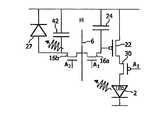
図3の画素回路で、フォトダイオード27は、コンデンサ24に蓄積されたゲート電圧を放電し、輝度を低減させる。表示素子2は、駆動トランジスタ22(Tdrive)のゲート電圧が閾値電圧に達すると、もはや発光しない。次いで、蓄積コンデンサ24は放電をやめる。電荷がフォトダイオード27から放出される割合は表示素子出力の関数であるから、フォトダイオード27は光受フィードバックデバイスとして機能する。駆動トランジスタ22がオフに切り替えられると、表示素子の陽極電圧は下がり、放電トランジスタ29はオンする。従って、蓄積コンデンサ24の残りの電荷は急速に失われ、発光はオフされる。この放電トランジスタは実際には任意であり、次のアドレス指定相の前に画素のリセットを確実にするために用いられるが、これは必要とされないこともある。In the pixel circuit of FIG. 3, the
駆動トランジスタ22のゲート−ソース間電圧を保持するコンデンサが放電されるので、表示素子2に対する駆動電流は徐々に下がる。従って、輝度は次第に小さくなる。このことは、より低い平均光度をもたらす。 Since the capacitor that holds the gate-source voltage of the
図4は、本願出願人によって提案された回路を示す。かかる回路は一定の光出力を有し、光出力に依存して1度に電源を切る。 FIG. 4 shows a circuit proposed by the applicant. Such a circuit has a constant light output and turns off at once depending on the light output.
駆動トランジスタ22のゲート−ソース間電圧は、先と同じく、蓄積コンデンサ24に保持される。しかし、この回路では、このコンデンサ24は、充電トランジスタ34を用いて、充電ライン32から一定電圧へと充電される。従って、駆動トランジスタ22は、表示素子2が光るべき場合に、画素へ入力されるデータとは無関係な一定レベルへと駆動される。輝度は、デューティーサイクルを変えることによって、具体的に、駆動トランジスタ22がオフされる時間を変えることによって、制御される。 The gate-source voltage of the
駆動トランジスタ22は、蓄積コンデンサ24を放電する放電トランジスタ36を用いてオフされる。放電トランジスタ36がオンされると、コンデンサ24は急速に放電され、駆動トランジスタ22はオフされる。 The
放電トランジスタ36は、そのゲート電圧が十分な電圧に達する場合にオンされる。フォトダイオード27は表示素子2によって照射され、先と同じく、表示素子2の光出力に依存して光電流を発生させる。この光電流は放電コンデンサ40を充電し、ある時点で、コンデンサ40の両端の電圧は、放電トランジスタ36の閾値電圧に達して、放電トランジスタ36をオンに切り替える。この時間は、コンデンサ40にもともと蓄積されている電荷と、光電流とに依存する。また、光電流は、表示素子2の光出力に依存する。最初に、放電コンデンサ40はデータ電圧を蓄える。従って、初期データ及び光フィードバックは、両方とも、回路のデューティーサイクルに影響を及ぼす。 The
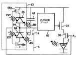
図5は、画素の光フィードバック部分(フォトダイオード27及び関連するコンデンサ42)が、列データライン6を用いて外部回路へ情報を提供するところの配置を示す。光フィードバック情報は監視され、この情報は、異なる補償効果を提供するよう画素へ印加されるデータを変更するために使用される。光フィードバック情報は、アドレストランジスタ16aによってデータ列から分離された画素により得られ、この配置は、データがフィードバック相の間に列へ供給されることを可能にするよう第2のアドレストランジスタ16bを有する。画素回路は、また、断路トランジスタ30を有する。断路トランジスタ30は、リセット中及びデータが画素へロードされている間に、表示素子からの如何なる光出力も阻止するために使用される。図5の断路トランジスタ30は、図4の回路でも使用され得る。 FIG. 5 shows an arrangement where the optical feedback portion of the pixel (
光フィードバックを備えた画素回路について多数の代替の実施形態が存在する。図3乃至5はp形トランジスタによる実施を示すが、例えばアモルファスシリコントランジスタに関して、n形トランジスタによる実施も存在する。 There are many alternative embodiments for pixel circuits with optical feedback. Although FIGS. 3-5 show implementations with p-type transistors, there are also implementations with n-type transistors, for example with respect to amorphous silicon transistors.
ここで、本発明について、概して図6を参照して説明する。 The present invention will now be described generally with reference to FIG.
図6の回路は、外部照射の影響が除去されることを可能にする汎用回路を示す。 The circuit of FIG. 6 shows a general purpose circuit that allows the effects of external illumination to be eliminated.
画素回路は、電流によって駆動される発光表示素子2と、駆動トランジスタ22と、断路トランジスタ30とを有する。駆動トランジスタ22のゲートへ印加される電圧を制御するよう、汎用回路ブロック60が示されており、この汎用回路ブロック60は、光依存性のデバイス配置62から電荷フローを受け取る。光依存性のデバイス配置62は、表示素子の輝度を検出する。コンデンサ63は、光依存性のデバイス配置62に結合されている。 The pixel circuit includes a light emitting
この回路で、断路トランジスタ30は、表示素子からパルス光出力を供給するために使用される。光依存性のデバイス配置62は、また、周期の間の光依存性のデバイス配置62の一定照射のためにネット出力電荷フローが実質的に零であるように、周期的に制御される。 In this circuit, the
これを達成するために、配置62は、両方の方向において出力ノード64へ/から電荷フローを供給することができる。図6の例で、光依存性のデバイス配置62は、電力線の間に同じ極性を有して直列に配置された第1及び第2のフォトダイオード66、68を有する。出力ノード64は、フォトダイオードの間の接点にある。フォトダイオードは両方とも、それらが接続されている電力線によって逆バイアスをかけられるが、電荷フロー経路は、1度に1つの電力線にしか提供されない。従って、少数キャリア電流は、1度に1つのフォトダイオードにしか流れることができない。示されるように、各フォトダイオードは、夫々のトランジスタ66a、68aを介してその電力線へ接続されており、これらのトランジスタは、相補的に切り替えられる。これを実現する1つの方法は、反対のタイプのトランジスタを設け、且つ、共通の制御信号を有することである。 To accomplish this, the
共通の制御信号は、周期的に交互にフォトダイオードを作動させる。2つのフォトダイオードに一定の照射がある場合、周期の当該期間に亘って平均されるコンデンサ63へのネット電荷フローは零である。 A common control signal periodically activates the photodiodes. If there is constant illumination of the two photodiodes, the net charge flow to the
しかし、表示素子の出力はパルス切替えをなされており、従って、表示素子の出力は、常に、フォトダイオードの唯1つの作動にタイミングが合っている。従って、表示出力によって、コンデンサ63への、又はコンデンサ63からのネット電荷フローが存在し、フィードバック・スキーマが実施され得る。 However, the output of the display element is pulse switched, so the output of the display element is always timed with only one operation of the photodiode. Thus, depending on the display output, there is a net charge flow to or from
この配置は、パルス光出力を使用し、対応するパルス光入力にのみ応答して動作するよう光フィードバックを配置する。このようにして、動作の周期の時間期間に亘って一様である周辺光は、光フィードバックシステムに影響を及ぼさない。このようにして、システムは、周辺光の状態によって影響を及ぼされない。 This arrangement uses pulsed light output and arranges optical feedback to operate only in response to the corresponding pulsed light input. In this way, ambient light that is uniform over the time period of the cycle of operation does not affect the optical feedback system. In this way, the system is not affected by ambient light conditions.
図6の例で、トランジスタ66a、68aは、断路トランジスタ30を制御するために使用される同じ制御信号によって制御される。断路トランジスタ30は、表示素子に対するパルスタイミング制御信号を供給する。これは、光出力の特性に対する光フィードバックの依存に結びつく。 In the example of FIG. 6,
この共有される制御ラインは、特定の周波数の矩形波により動作する。 This shared control line operates with a rectangular wave of a specific frequency.
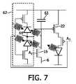
汎用回路ブロック60は、例えば、図2乃至5の回路を実施するよう、多種多様な方法で実施され得る。図7に示される最も簡単な実施では、ブロック60は、単に、ノード64と、駆動トランジスタ22のゲートとの間の接続である。この最も基本的な回路実施は、放電トランジスタ20を用いない図3の回路に対応する。 The general
図8は、どのようにブロック60が、図4を参照して説明される動作に対応する回路動作を提供するよう実施されるかを示す。 FIG. 8 illustrates how
図7及び8に示される回路は、断路トランジスタ30が印加される矩形波制御信号を有する場合に、光出力を変調する。光出力が十分に高い周波数にあるならば、これは目には見えない。しかし、図7における最も基本的な回路は、極めて急な光度減衰を有するので、図8のスナップオフ回路と同様に動作することができない。 The circuits shown in FIGS. 7 and 8 modulate the light output when the
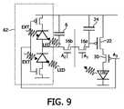
図9は、図5を参照して説明された外部監視技術に基づく本発明の実施を示す。図9の回路は、ディスプレイが、例えば当該ディスプレイのスイッチオン又はスイッチオフで、通常使用にない場合に測定相を実行することによって、当該回路が光出力を変調しないように配置される。この測定相は、表示素子及び駆動トランジスタのより長期のエージング効果を補償するために使用される場合、高い周波数を有して実施される必要はない。 FIG. 9 shows an implementation of the invention based on the external monitoring technique described with reference to FIG. The circuit of FIG. 9 is arranged so that the circuit does not modulate the light output by performing the measurement phase when the display is not in normal use, for example when the display is switched on or off. This measurement phase need not be implemented with a high frequency when used to compensate for the longer term aging effects of the display element and the drive transistor.
上記回路は全て、電荷フローの相殺を提供するためにダブル・フォトダイオードを使用する。この概念は、代わりに、単一の感光性の薄膜トランジスタ(TFT)によって実施されても良い。 All of the above circuits use double photodiodes to provide charge flow cancellation. This concept may alternatively be implemented by a single photosensitive thin film transistor (TFT).
図10は、感光性トランジスタの使用のための汎用回路を示す。感光性トランジスタは、動作周期に依存して対向方向で光電流を供給するよう制御され得る。 FIG. 10 shows a general purpose circuit for the use of a photosensitive transistor. The photosensitive transistor can be controlled to supply a photocurrent in the opposite direction depending on the operating period.
フォトトランジスタ80は、先と同じく、コンデンサ63を充電又は放電するよう、ノード64へ電流を、あるいはノード64からドレイン電流を供給する。ソース端子及びドレイン端子のバイアスに依存して、トランジスタ80はいずれか一方の方向で導通することができ、感光性漏れ電流は、このようにして、いずれか一方の方向で流され得る。これは、ゲート電圧と同様にソース−ドレイン間電圧の制御を必要とする。これを達成するために、トランジスタ80は、ノード64と位相ライン82との間に接続されている。 As before, the
TFT80は、1つの相ではノード64へ電流を供給し、他の相ではノード64から電流を吸い込むように配置される。表示素子2からの光は、照射相の間、TFT80に入射し、外部光(EXT)は、また、その間ずっとフォトTFT80に入射する。位相ライン82は、TFT80のバイアスを制御する。TFT80は、適切なゲート制御信号によって常にオフを保たれる。 The
位相ラインの電圧がノード電圧を上回ると、TFT80は電流をノードに供給する。他の相で、位相ラインの電圧はノード電圧を下回っており、従って、TFT80はノードからの電流を吸い込む。これは、ゲート電圧を極めて低く保つことによって達成され得る。しかし、これは、各相の間でバイアス状態を変化させ、画素の動作に悪影響を及ぼしうる。 When the voltage on the phase line exceeds the node voltage, the
理想的な状態は、各相に関して同じゲート−ソース間電圧を保つよう、直接にゲート電圧を制御することである。 The ideal condition is to control the gate voltage directly to keep the same gate-source voltage for each phase.
図10は、この理想的な状態を達成する1つの方法を示す。図10で、ゲート電圧は、表示素子2の陽極へ接続されている。一例として、電源電圧は10Vであり、ノード電圧は約5V(なお、この電圧は、画素動作の間変動しうる。)であるよう配置されるとする。その場合、位相ライン82は、TFT80が正確に電流を供給し且つ吸い込むことを確実にするよう、10Vから0Vの間を動くことができる。その場合、ゲート電圧は、理想的には5Vから0Vの間を動き、TFTにおいて同じゲート−ソース間状態を提供する。即ち、ゲート電圧は、n形TFTをまさにオフに保つためにソース電圧に等しい。表示素子2の陽極は、LED2がオンである場合に約5Vにあり、LED2がオフである場合には0Vにある。従って、表示素子2の陽極は、このような正確なバイアスをおおよそ与えることができる。 FIG. 10 shows one way to achieve this ideal condition. In FIG. 10, the gate voltage is connected to the anode of the
上述される回路は、発振の期間に亘って一定である外部光のみを相殺することができ、これは、パルス/周期制御ラインにおける矩形波期間がほぼライン時間(例えば、10マイクロ秒。)程度である場合に、ほぼ全ての種類の外部光に関して十分である。しかし、他の画素にある表示素子は、まさに同じ周波数で変調光を生成しており、これは、このような光が他の画素に達することができる場合に相殺され得ない。 The circuit described above can only cancel out external light that is constant over the period of oscillation, which is about a line time (eg, 10 microseconds) for the rectangular wave period in the pulse / period control line. Is sufficient for almost all types of external light. However, display elements in other pixels are producing modulated light at exactly the same frequency, and this cannot be offset if such light can reach other pixels.
画素間で光を遮断することは、画素設計の物理的構造を用いて達成され得る。しかし、これは、以下で説明されるように、フィードバック方式を変更することによって回避され得る。 Blocking light between pixels can be accomplished using the physical structure of the pixel design. However, this can be avoided by changing the feedback scheme, as described below.
具体的に、隣り合う画素は、関心のある画素にある感光性デバイスに光を漏らすことがある。他の解決法は、全ての隣り合う画素が、異なる位相を用いてそれらの光出力を変調するように、画素を配置することである。 Specifically, adjacent pixels may leak light to the photosensitive device at the pixel of interest. Another solution is to arrange the pixels so that all neighboring pixels modulate their light output using different phases.
具体的に、1つの画素が、隣の画素とは位相が90度ずれて動作する場合、その1つの画素の出力は、照射時間の半分が、隣の画素の1つの作動しているフォトダイオードに対応し、照射時間の残り半分が、他の作動しているフォトダイオードに対応するように、タイミングを合わせられる。 Specifically, when one pixel operates 90 degrees out of phase with an adjacent pixel, the output of the one pixel is a photodiode in which one of the adjacent pixels operates for half the irradiation time. And the other half of the illumination time is timed to correspond to other active photodiodes.
このアプローチを実施するよう、異なるグループの画素は、単に、位相がずれたパルス及びフィードバック制御(制御ラインA3)を必要とする。従って、2つの組の画素は、異なるタイミングの光パルス及びフィードバック制御を有して定義される。 To implement this approach, different groups of pixels simply require out-of-phase pulses and feedback control (control line A3). Thus, the two sets of pixels are defined with different timing light pulses and feedback control.
隣接する画素間に有効な遮蔽を提供するよう、2つの組の画素は、図11に示されるように、格子状のパターンを有することができる。1つの組の画素は+記号によって表され、他の組の画素は−記号によって表される。図11は、また、3つのRGBサブピクセルの線形配列として形成される画素を示し、位相パターンは、個々のサブピクセルレベルにおいて適用される。 To provide effective shielding between adjacent pixels, the two sets of pixels can have a grid pattern, as shown in FIG. One set of pixels is represented by a + symbol and the other set of pixels is represented by a-symbol. FIG. 11 also shows the pixels formed as a linear array of three RGB subpixels, with the phase pattern applied at the individual subpixel level.
これは、各画素のパルス出力が、夫々の側にある画素及び配列において上下にある画素のパルス出力とは位相がずれることを可能にする。1つの組の表示画素のパルス出力は、他の組の表示画素のパルス出力とは位相が90度ずれることができる。 This allows the pulse output of each pixel to be out of phase with the pulse outputs of the pixels on the respective side and the pixels above and below in the array. The pulse output of one set of display pixels can be 90 degrees out of phase with the pulse output of the other set of display pixels.
このようなクロストークの除去は、例えば異なる行といった、異なるグループの画素において発振の周波数を変更することによって、より向上し得る。行nで、パルス/周期制御ラインが周波数fで発振する場合、ラインn−1及びn+1で、パルス/周期制御ラインは周波数2f又はf/2で発振することができる。 Such crosstalk removal can be further improved by changing the frequency of oscillation in different groups of pixels, eg, different rows. In row n, if the pulse / period control line oscillates at frequency f, on lines n−1 and n + 1, the pulse / period control line can oscillate at frequency 2f or f / 2.
本発明の駆動方式は、パルスの連続として画素の電流駆動式の発光表示素子に電流を流すことと、光依存性のデバイス配置を用いて前記表示素子の輝度を検出することとを含み、前記光依存性のデバイス配置は、周期的に制御され、前記表示素子の輝度に依存して出力電荷フローを供給する。前記表示素子を流れる電流の駆動は、前記光依存性のデバイス配置の出力に応答して制御され、この出力は、周辺の又は他の実質的に時間一定の照射に影響されない。 The driving method of the present invention includes passing a current through a current-driven light-emitting display element of a pixel as a series of pulses, and detecting the luminance of the display element using a light-dependent device arrangement, The light-dependent device arrangement is periodically controlled to provide output charge flow depending on the brightness of the display element. Driving the current through the display element is controlled in response to the output of the light-dependent device arrangement, and this output is unaffected by the surrounding or other substantially time-constant illumination.
上記から明らかなように、フォトダイオード光センサ、又はアモルファスシリコンフォトTFTが使用され得る。かかるTFTにおいて、ソースとドレインとの間のチャネルで吸収される光子は、ソース電極及びドレイン電極によって検知され得る光電流を生成する。光電流は、また、アモルファスシリコン層の上部においてゲート電極によって影響を及ぼされ、従って、動作の均衡を保つことができる。低温ポリシリコンフォトTFTは、また、感光性のデバイスとして使用され得る。 As is apparent from the above, a photodiode photosensor or an amorphous silicon photo TFT can be used. In such a TFT, photons absorbed in the channel between the source and drain generate a photocurrent that can be detected by the source and drain electrodes. The photocurrent is also affected by the gate electrode on top of the amorphous silicon layer, and can thus balance the operation. Low temperature polysilicon photo TFTs can also be used as photosensitive devices.
本発明のディスプレイ装置は、持ち運び可能な用途(携帯電話、PDA、デジタルカメラ)で、(ラップトップ)モニタで、及びテレビで、フラットパネルディスプレイとして特定の用途を見出す。 The display device of the present invention finds particular use as a flat panel display in portable applications (cell phones, PDAs, digital cameras), (laptop) monitors, and in televisions.
本発明のディスプレイ装置の製造に含まれる工程は、それらが所謂当業者にとって周知であるので、本願では記載されない。アモルファスシリコン、ポリシリコン、微結晶性シリコン又は他の半導体トランジスタ技術が採用されても良い。本発明は、感光性デバイスが夫々の画素に関してフィードバック素子として使用されるところの如何なる画素回路へも適用され得る。 The steps involved in the manufacture of the display device of the present invention are not described herein because they are well known to those skilled in the art. Amorphous silicon, polysilicon, microcrystalline silicon, or other semiconductor transistor technology may be employed. The invention can be applied to any pixel circuit where the photosensitive device is used as a feedback element for each pixel.
本開示を読むことで、他の変形例が当業者には明らかであろう。かかる変形例は、アクティブマトリクスELディスプレイ装置及びその構成要素部の分野で既に知られており、本願に記載される特徴に代わって、あるいはそれらに加えて使用され得る他の特徴を含んでも良い。 From reading the present disclosure, other modifications will be apparent to persons skilled in the art. Such variations are already known in the field of active matrix EL display devices and component parts thereof, and may include other features that may be used in place of or in addition to the features described herein.
Claims (25)
Translated fromJapanese夫々の画素は:
電流によって駆動される発光表示素子;
前記表示素子の輝度を検出し、前記表示素子の前記輝度に依存して出力電荷フローを供給する光依存性のデバイス配置;及び
前記表示素子に電流を流す駆動トランジスタ,
を有し、
前記駆動トランジスタは、前記光依存性のデバイス配置の出力に応答して制御され、
前記電流によって駆動される発光表示素子は、パルス出力を供給するよう制御され、
前記光依存性のデバイス配置は、周期の間の前記光依存性のデバイス配置の一定照射のために、実質的に零のネット出力電荷フローが存在するように、周期的に制御される、アクティブマトリクスディスプレイ装置。An active matrix display device having an array of display pixels,
Each pixel is:
A light-emitting display element driven by a current;
A light-dependent device arrangement for detecting the brightness of the display element and supplying an output charge flow depending on the brightness of the display element; and a drive transistor for passing current through the display element;
Have
The drive transistor is controlled in response to an output of the light dependent device arrangement;
The light emitting display element driven by the current is controlled to supply a pulse output,
The light-dependent device arrangement is periodically controlled such that there is substantially zero net output charge flow for constant illumination of the light-dependent device arrangement during a period. Matrix display device.
前記周期的な制御は、交互に前記フォトダイオードを作動させる、請求項1乃至3のうちいずれか一項記載のアクティブマトリクスディスプレイ装置。The light-dependent device arrangement has first and second photodiodes in series between power lines, and receives an output from the arrangement at a contact point between the first and second photodiodes,
The active matrix display device according to claim 1, wherein the periodic control alternately operates the photodiodes.
前記パルストランジスタは、パルスタイミング制御信号によって切り替えられる、請求項1乃至5のうちいずれか一項記載のアクティブマトリクスディスプレイ装置。The drive transistor, the display element, and the pulse transistor are in series between power lines,
The active matrix display device according to claim 1, wherein the pulse transistor is switched by a pulse timing control signal.
前記フォトトランジスタのゲートは、周期的な制御信号を供給される、請求項7記載のアクティブマトリクスディスプレイ装置。The phototransistor is connected between a phototransistor control line and an output of the arrangement;
The active matrix display device according to claim 7, wherein a gate of the phototransistor is supplied with a periodic control signal.
前記パルストランジスタは、パルスタイミング制御信号によって切り替えられる、請求項7又は8記載のアクティブマトリクスディスプレイ装置。The drive transistor, the display element, and the pulse transistor are in series between power lines,
The active matrix display device according to claim 7 or 8, wherein the pulse transistor is switched by a pulse timing control signal.
1つの組の表示画素のパルス出力は、他の組の表示画素のパルス出力とは位相がずれている、請求項1乃至10のうちいずれか一項記載のアクティブマトリクスディスプレイ装置。The array of display pixels has at least a first and a second set of display pixels,
The active matrix display device according to claim 1, wherein a pulse output of one set of display pixels is out of phase with a pulse output of another set of display pixels.
1つのグループの表示画素のパルス出力は、他のグループの表示画素のパルス出力とは異なる周波数にある、請求項1乃至14のうちいずれか一項記載のアクティブマトリクスディスプレイ装置。The array of display pixels includes at least first and second groups of display pixels,
The active matrix display device according to claim 1, wherein the pulse output of the display pixels of one group is at a different frequency from the pulse output of the display pixels of the other group.
パルスの連続として前記画素の電流駆動式の発光表示素子に電流を流すステップ;
周期的に制御され、且つ、前記表示素子の輝度に依存して出力電荷フローを供給する光依存性のデバイス配置によって、前記表示素子の輝度を検出するステップ;及び
前記光依存性のデバイス配置の出力に応答して前記表示素子を流れる前記電流の駆動を制御するステップ,
を有し、
周期の間の前記光依存性のデバイス配置の一定照射のために、実質的に零のネット出力電荷フローが存在する、方法。A method of driving the pixels of an active matrix display device having an array of pixels, comprising:
Passing a current through the current-driven light emitting display element of the pixel as a series of pulses;
Detecting the brightness of the display element by means of a light-dependent device arrangement that is periodically controlled and that provides an output charge flow depending on the brightness of the display element; and Controlling the driving of the current flowing through the display element in response to an output;
Have
A method wherein there is substantially zero net output charge flow for constant illumination of the light dependent device arrangement during a period.
前記駆動トランジスタ、前記表示素子、及び前記パルストランジスタは、電力線の間で直列である、請求項18乃至22のうちいずれか一項記載の方法。The step of passing a current through the current-driven light emitting display element of the pixel as a continuation of the pulse has a step of switching a pulse transistor by a pulse timing control signal,
23. A method according to any one of claims 18 to 22, wherein the drive transistor, the display element, and the pulse transistor are in series between power lines.
Applications Claiming Priority (2)
| Application Number | Priority Date | Filing Date | Title |
|---|---|---|---|
| EP05105971 | 2005-06-30 | ||
| PCT/IB2006/051924WO2007004085A2 (en) | 2005-06-30 | 2006-06-15 | Electroluminescent display devices |
Publications (1)
| Publication Number | Publication Date |
|---|---|
| JP2009500650Atrue JP2009500650A (en) | 2009-01-08 |
Family
ID=37492441
Family Applications (1)
| Application Number | Title | Priority Date | Filing Date |
|---|---|---|---|
| JP2008519024AWithdrawnJP2009500650A (en) | 2005-06-30 | 2006-06-15 | Electroluminescent display device |
Country Status (6)
| Country | Link |
|---|---|
| US (1) | US20100177075A1 (en) |
| EP (1) | EP1904997A2 (en) |
| JP (1) | JP2009500650A (en) |
| CN (1) | CN101208735A (en) |
| TW (1) | TW200710805A (en) |
| WO (1) | WO2007004085A2 (en) |
Cited By (1)
| Publication number | Priority date | Publication date | Assignee | Title |
|---|---|---|---|---|
| WO2023079674A1 (en)* | 2021-11-05 | 2023-05-11 | シャープディスプレイテクノロジー株式会社 | Display device and driving method therefor |
Families Citing this family (13)
| Publication number | Priority date | Publication date | Assignee | Title |
|---|---|---|---|---|
| US20110012879A1 (en)* | 2008-04-10 | 2011-01-20 | Masaki Uehata | Display device having optical sensors |
| JP5272885B2 (en)* | 2009-05-12 | 2013-08-28 | ソニー株式会社 | Display device and control method of light detection operation |
| CN103413519B (en) | 2013-07-18 | 2016-05-11 | 京东方科技集团股份有限公司 | A kind of image element circuit and driving method, array base palte and display unit |
| US10431164B2 (en)* | 2016-06-16 | 2019-10-01 | Semiconductor Energy Laboratory Co., Ltd. | Display device, display module, and electronic device |
| CN106935190B (en)* | 2017-02-22 | 2019-02-05 | 上海天马有机发光显示技术有限公司 | A kind of organic light emitting display panel, organic light-emitting display device, organic light emitting display panel driving method |
| CN110164362B (en) | 2018-06-26 | 2021-08-17 | 京东方科技集团股份有限公司 | Compensation device and method for light-emitting device, display substrate and manufacturing method thereof |
| KR102662881B1 (en)* | 2018-12-31 | 2024-05-03 | 엘지디스플레이 주식회사 | pixel circuit including optical fingerprint sensing circuit, Method for driving the pixel circuit and Display device |
| KR20210064483A (en) | 2019-11-25 | 2021-06-03 | 삼성디스플레이 주식회사 | Display panel having input sensing function and display device |
| CN114078414A (en)* | 2021-11-22 | 2022-02-22 | 武汉华星光电技术有限公司 | Ambient light monitoring circuit and display panel with same |
| CN114170939B (en)* | 2021-12-02 | 2023-05-30 | 武汉华星光电技术有限公司 | Ambient light monitoring circuit and display panel with same |
| CN116013195A (en)* | 2021-12-08 | 2023-04-25 | 武汉天马微电子有限公司 | Display device and control method thereof |
| TWI872759B (en)* | 2022-11-04 | 2025-02-11 | 大陸商廣州印芯半導體技術有限公司 | Display device capable of in-display sensing |
| CN115831979B (en)* | 2022-12-21 | 2023-09-08 | 惠科股份有限公司 | Array substrate, manufacturing method, pixel driving circuit and display panel |
Family Cites Families (10)
| Publication number | Priority date | Publication date | Assignee | Title |
|---|---|---|---|---|
| US6307528B1 (en)* | 1997-12-08 | 2001-10-23 | Hughes Electronics Corporation | Contrast organic light-emitting display |
| US7012600B2 (en)* | 1999-04-30 | 2006-03-14 | E Ink Corporation | Methods for driving bistable electro-optic displays, and apparatus for use therein |
| GB9923261D0 (en) | 1999-10-02 | 1999-12-08 | Koninkl Philips Electronics Nv | Active matrix electroluminescent display device |
| WO2001058143A1 (en)* | 2000-02-07 | 2001-08-09 | D.L. Ventures, Inc. | Virtual reality portrait |
| GB0014962D0 (en)* | 2000-06-20 | 2000-08-09 | Koninkl Philips Electronics Nv | Matrix array display devices with light sensing elements and associated storage capacitors |
| GB2381644A (en)* | 2001-10-31 | 2003-05-07 | Cambridge Display Tech Ltd | Display drivers |
| EP1547057A1 (en) | 2002-09-23 | 2005-06-29 | Koninklijke Philips Electronics N.V. | Matrix display device with photosensitive element |
| GB0307789D0 (en) | 2003-04-04 | 2003-05-07 | Koninkl Philips Electronics Nv | Electroluminescent display devices |
| KR20060123726A (en)* | 2003-09-25 | 2006-12-04 | 코닌클리케 필립스 일렉트로닉스 엔.브이. | Color display screen with multiple cells |
| US7545396B2 (en)* | 2005-06-16 | 2009-06-09 | Aurora Systems, Inc. | Asynchronous display driving scheme and display |
- 2006
- 2006-06-15JPJP2008519024Apatent/JP2009500650A/ennot_activeWithdrawn
- 2006-06-15EPEP06765756Apatent/EP1904997A2/ennot_activeWithdrawn
- 2006-06-15USUS11/993,640patent/US20100177075A1/ennot_activeAbandoned
- 2006-06-15CNCNA2006800231705Apatent/CN101208735A/enactivePending
- 2006-06-15WOPCT/IB2006/051924patent/WO2007004085A2/ennot_activeApplication Discontinuation
- 2006-06-27TWTW095123161Apatent/TW200710805A/enunknown
Cited By (1)
| Publication number | Priority date | Publication date | Assignee | Title |
|---|---|---|---|---|
| WO2023079674A1 (en)* | 2021-11-05 | 2023-05-11 | シャープディスプレイテクノロジー株式会社 | Display device and driving method therefor |
Also Published As
| Publication number | Publication date |
|---|---|
| WO2007004085A2 (en) | 2007-01-11 |
| US20100177075A1 (en) | 2010-07-15 |
| TW200710805A (en) | 2007-03-16 |
| CN101208735A (en) | 2008-06-25 |
| EP1904997A2 (en) | 2008-04-02 |
| WO2007004085A3 (en) | 2007-03-15 |
Similar Documents
| Publication | Publication Date | Title |
|---|---|---|
| JP2009500650A (en) | Electroluminescent display device | |
| EP1444683B1 (en) | Display driver circuits for electro-optic displays | |
| KR101937336B1 (en) | Emission-control circuit, display device having the same, and driving method thereof | |
| US20080203930A1 (en) | Electroluminescent Display Devices | |
| US7602387B2 (en) | Electroluminescent display devices | |
| JP2007535714A (en) | Improved stable active matrix light emitting display | |
| US7242145B2 (en) | Color electroluminescent display devices | |
| JP2001075524A (en) | Display device | |
| US20060164344A1 (en) | Electroluminescent display devices | |
| JP2010511183A (en) | Active matrix display device having optical feedback and driving method thereof | |
| JP2008501994A (en) | Active matrix display device | |
| JP2009511978A (en) | Radiation display device | |
| WO2002075711A1 (en) | Selfluminous display device | |
| JP2006520490A (en) | Luminescent active matrix display with timing effective optical feedback to combat aging | |
| GB2453372A (en) | A pixel driver circuit for active matrix driving of an organic light emitting diode (OLED) | |
| JP2006523321A (en) | Active matrix display device | |
| JP2006500610A (en) | Matrix display element with photosensitive element | |
| JP2007524118A (en) | Active matrix display device | |
| JP2009514004A (en) | Active matrix display device | |
| US7839367B2 (en) | Active matrix display devices | |
| JP2008527400A (en) | light source | |
| JP2007519955A (en) | Luminescent display device | |
| HK1069000B (en) | Display driver circuits for electro-optic displays |
Legal Events
| Date | Code | Title | Description |
|---|---|---|---|
| A621 | Written request for application examination | Free format text:JAPANESE INTERMEDIATE CODE: A621 Effective date:20090612 | |
| A761 | Written withdrawal of application | Free format text:JAPANESE INTERMEDIATE CODE: A761 Effective date:20090730 |