JP2009295221A - Semiconductor memory device - Google Patents
Semiconductor memory deviceDownload PDFInfo
- Publication number
- JP2009295221A JP2009295221AJP2008146611AJP2008146611AJP2009295221AJP 2009295221 AJP2009295221 AJP 2009295221AJP 2008146611 AJP2008146611 AJP 2008146611AJP 2008146611 AJP2008146611 AJP 2008146611AJP 2009295221 AJP2009295221 AJP 2009295221A
- Authority
- JP
- Japan
- Prior art keywords
- bit line
- voltage
- selection gate
- transistor
- cell
- Prior art date
- Legal status (The legal status is an assumption and is not a legal conclusion. Google has not performed a legal analysis and makes no representation as to the accuracy of the status listed.)
- Withdrawn
Links
Images


Classifications
- G—PHYSICS
- G11—INFORMATION STORAGE
- G11C—STATIC STORES
- G11C7/00—Arrangements for writing information into, or reading information out from, a digital store
- G11C7/06—Sense amplifiers; Associated circuits, e.g. timing or triggering circuits
- G—PHYSICS
- G11—INFORMATION STORAGE
- G11C—STATIC STORES
- G11C16/00—Erasable programmable read-only memories
- G11C16/02—Erasable programmable read-only memories electrically programmable
- G11C16/04—Erasable programmable read-only memories electrically programmable using variable threshold transistors, e.g. FAMOS
- G11C16/0483—Erasable programmable read-only memories electrically programmable using variable threshold transistors, e.g. FAMOS comprising cells having several storage transistors connected in series
- G—PHYSICS
- G11—INFORMATION STORAGE
- G11C—STATIC STORES
- G11C16/00—Erasable programmable read-only memories
- G11C16/02—Erasable programmable read-only memories electrically programmable
- G11C16/06—Auxiliary circuits, e.g. for writing into memory
- G11C16/08—Address circuits; Decoders; Word-line control circuits
- G—PHYSICS
- G11—INFORMATION STORAGE
- G11C—STATIC STORES
- G11C16/00—Erasable programmable read-only memories
- G11C16/02—Erasable programmable read-only memories electrically programmable
- G11C16/06—Auxiliary circuits, e.g. for writing into memory
- G11C16/26—Sensing or reading circuits; Data output circuits
- G11C16/28—Sensing or reading circuits; Data output circuits using differential sensing or reference cells, e.g. dummy cells
- G—PHYSICS
- G11—INFORMATION STORAGE
- G11C—STATIC STORES
- G11C16/00—Erasable programmable read-only memories
- G11C16/02—Erasable programmable read-only memories electrically programmable
- G11C16/06—Auxiliary circuits, e.g. for writing into memory
- G11C16/30—Power supply circuits
- G—PHYSICS
- G11—INFORMATION STORAGE
- G11C—STATIC STORES
- G11C2207/00—Indexing scheme relating to arrangements for writing information into, or reading information out from, a digital store
- G11C2207/06—Sense amplifier related aspects
- G11C2207/068—Integrator type sense amplifier
Landscapes
- Engineering & Computer Science (AREA)
- Microelectronics & Electronic Packaging (AREA)
- Read Only Memory (AREA)
Abstract
Translated fromJapaneseDescription
Translated fromJapaneseこの発明は、半導体記憶装置に係り、特に大容量化した記憶装置でのビット線抵抗の影響を考慮したセンス方式に関する。 The present invention relates to a semiconductor memory device, and more particularly, to a sensing method that takes into account the influence of bit line resistance in a memory device with an increased capacity.
電気的書き換え可能な不揮発性半導体記憶装置(EEPROM)の一つとして、NAND型フラッシュメモリが知られている。NAND型フラッシュメモリの読み出しや書き込みベリファイに用いられるセンスアンプとして、選択メモリセルに例えば0.5Vのドレイン・ソース間電圧を印加して選択メモリセルが流すセル電流を判定する、電流検出型センスアンプが知られている(例えば特許文献1参照)。このセンス方式では、センス時の選択メモリセルのドレイン・ソース間電圧は、ビット線端にあるセンスアンプ内のクランプトランジスタのゲート電圧によって制御する。 NAND flash memory is known as one of electrically rewritable nonvolatile semiconductor memory devices (EEPROM). As a sense amplifier used for reading or writing verification of a NAND flash memory, a current detection type sense amplifier that applies a drain-source voltage of, for example, 0.5 V to a selected memory cell and determines a cell current flowing through the selected memory cell Is known (see, for example, Patent Document 1). In this sense system, the drain-source voltage of the selected memory cell at the time of sensing is controlled by the gate voltage of the clamp transistor in the sense amplifier at the bit line end.
微細化・高集積化・大容量化が進んでいるNAND型フラッシュメモリにおいては、ビット線抵抗が高抵抗化し、ビット線抵抗による電圧降下によってメモリセルのドレイン・ソース間電圧の制御がしにくくなってきている。実際に従来のセンス方式では、メモリセルのドレイン・ソース間に印加される電圧は、ビット線抵抗による電圧降下の分だけクランプ電圧よりも低くなってしまう。 In NAND flash memory, which is becoming more miniaturized, highly integrated, and larger in capacity, the bit line resistance becomes higher, and the voltage drop due to the bit line resistance makes it difficult to control the drain-source voltage of the memory cell. It is coming. Actually, in the conventional sense system, the voltage applied between the drain and source of the memory cell becomes lower than the clamp voltage by the amount of voltage drop due to the bit line resistance.
これにより、メモリセルのドレイン・ソース間電圧が実質的に減ると、セル電流が減少し、例えば十分にしきい値電圧の低い消去セルであっても消去セルとして読まれない、といった誤読み出しが起こる可能性がある。
この発明は、誤読み出しの可能性を低減した半導体記憶装置を提供することを目的とする。 An object of the present invention is to provide a semiconductor memory device in which the possibility of erroneous reading is reduced.
この発明の一態様による半導体記憶装置は、
選択ゲートトランジスタを介してビット線に接続されるメモリセルと、
前記ビット線に電流を供給するための電流源を備えて、前記メモリセルのセル電流によってそのセルデータを検知するセンスアンプと、
読み出し時、前記メモリセルのドレイン・ソース間電圧を前記ビット線の抵抗によらず実質的に一定に保つように、前記選択ゲートトランジスタのゲートを駆動する選択ゲート線ドライバと、
を有することを特徴とする。A semiconductor memory device according to one embodiment of the present invention includes:
A memory cell connected to a bit line via a select gate transistor;
A sense amplifier that includes a current source for supplying current to the bit line, and that senses cell data based on a cell current of the memory cell;
A selection gate line driver that drives the gate of the selection gate transistor so that the drain-source voltage of the memory cell is kept substantially constant regardless of the resistance of the bit line at the time of reading;
It is characterized by having.
この発明によると、誤読み出しの可能性を低減した半導体記憶装置を提供することができる。 According to the present invention, a semiconductor memory device with reduced possibility of erroneous reading can be provided.
以下、図面を参照して、この発明の実施の形態を説明する。 Embodiments of the present invention will be described below with reference to the drawings.
図1は、一実施の形態によるNAND型フラッシュメモリの機能ブロックを示し、図2はそのメモリコア部の構成を示している。メモリセルアレイ1は、図2に示すように、複数のメモリセルM0−M31が直列接続されたNANDセルユニット(NANDストリング)NUを配列して構成されている。 FIG. 1 shows a functional block of a NAND flash memory according to one embodiment, and FIG. 2 shows a configuration of the memory core unit. As shown in FIG. 2, the
メモリセルは、浮遊ゲートと制御ゲートが積層されたMOSトランジスタ構造を有し、その浮遊ゲートに電子を注入してしきい値を高くした状態と、電子を放出させてしきい値を低くした状態とを、データとして利用する。或いは浮遊ゲート構造に代わって、ゲート絶縁膜内に電荷トラップを備えて、同様のデータ記憶を行うセル構造を用いることも出来る。 The memory cell has a MOS transistor structure in which a floating gate and a control gate are stacked, in which electrons are injected into the floating gate to increase the threshold value, and electrons are emitted to reduce the threshold value. Are used as data. Alternatively, instead of the floating gate structure, a cell structure in which a charge trap is provided in the gate insulating film and similar data storage is performed can be used.
NANDストリングNUの一端は、選択ゲートトランジスタS1を介してビット線BLに接続され、他端は選択ゲートトランジスタS2を介して共通ソース線CELSRCに接続されている。メモリセルM0−M31の制御ゲートはそれぞれワード線WL0−WL31に接続され、選択ゲートトランジスタS1,S2のゲートはそれぞれ選択ゲート線SGD,SGSに接続されている。 One end of the NAND string NU is connected to the bit line BL via the selection gate transistor S1, and the other end is connected to the common source line CELSRC via the selection gate transistor S2. The control gates of the memory cells M0 to M31 are connected to the word lines WL0 to WL31, respectively, and the gates of the selection gate transistors S1 and S2 are connected to the selection gate lines SGD and SGS, respectively.
ワード線及び選択ゲート線を選択駆動するためにロウデコーダ2が設けられている。ビット線BLは、センスアンプ回路3に接続されている。図2では、センスアンプ回路3として、ビット線毎に設けられた1ページ分のセンスアンプSAを有する例を示している。例えば隣接ビット線が一つのセンスアンプを共有し、一方のビット線が選択されてセンスアンプに接続される方式とすることもできる。 A
1ワード線により同時に選択されるメモリセルの集合は、1ページを構成し、これが同時読み出し及び書き込みの単位となる。ワード線を共有するNANDストリングの集合は、消去単位となるブロックを構成する。メモリセルアレイ1は通常、図2に示すようにビット線方向に複数のブロックBLK0−BLKnを配置して構成される。 A set of memory cells that are simultaneously selected by one word line constitutes one page, which is a unit for simultaneous reading and writing. A set of NAND strings sharing a word line constitutes a block serving as an erase unit. The
センスアンプ回路3の1ページの読み出しデータは、カラムデコーダ5により制御されてカラム単位でデータ線を転送され、I/Oバッファ9を介して外部I/Oパッドに出力される。書き込み時は、1ページの書き込みデータがカラム単位でI/Oバッファ9を介してセンスアンプ回路3にロードされる。 The read data for one page of the sense amplifier circuit 3 is controlled by the
I/Oバッファ9を介して入力されるコマンドは、コントローラ8でデコードされ、動作制御に供される。I/Oバッファ9を介して入力されるアドレスは、アドレスレジスタ6を介してロウデコーダ2及びカラムデコーダ5に送られる。 A command input via the I /
コントローラ8は、コントロールパッドから供給される各種制御信号(チップイネーブル、コマンドラッチイネーブル、アドレスラッチイネーブル、書き込みイネーブル、読み出しイネーブル等)及びコマンドに基づいて、読み出し制御及び書き込みや消去のシーケンス制御を行う。 The controller 8 performs read control and write / erase sequence control based on various control signals (chip enable, command latch enable, address latch enable, write enable, read enable, etc.) and commands supplied from the control pad.
各動作モードに必要な各種の高電圧を発生するために、高電圧発生回路7が設けられている。この高電圧発生回路7もコントローラ8により制御される。 A high voltage generation circuit 7 is provided to generate various high voltages necessary for each operation mode. The high voltage generation circuit 7 is also controlled by the controller 8.
コアコントロールドライバ4は、コントローラ8により制御されて、ロウデコーダ2で選択されたブロック内の各ワード線及び選択ゲート線を動作モードに応じて駆動する電圧を発生するドライブ回路である。 The core control driver 4 is a drive circuit that is controlled by the controller 8 and generates a voltage for driving each word line and selection gate line in the block selected by the
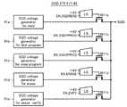
図4は、コアコントロールドライバ4内の一部、選択ゲート線(SGD)ドライバ40の構成を示している。動作モードに応じて選択ゲート線SGDを駆動するために、読み出し時のSGD電圧発生回路41、高速書き込み時のSGD電圧発生回路41b、低速書き込み時のSGD電圧発生回路41c、消去時のSGD電圧発生回路41d、消去ベリファイ時のSGD電圧発生回路41e等が用意される。 FIG. 4 shows a configuration of a part of the core control driver 4, the selection gate line (SGD) driver 40. In order to drive the selection gate line SGD according to the operation mode, the SGD voltage generation circuit 41 at the time of reading, the SGD
これらの電圧発生回路41a−41eの出力電圧は、それぞれレベルシフト回路LSにより駆動される転送トランジスタM11a−M11eにより、電圧降下なしの選択ゲート線SGDに転送されるようになっている。 The output voltages of these
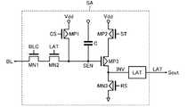
図3は、センスアンプSAの主要部構成を示している。これは、特許文献1に開示されているものと基本的に同じである。センスアンプSAは、クランプ用NMOSトランジスタMN1及びビット線切り離し用NMOSトランジスタMN2を介してビット線BLに接続されるセンスノードSENを有する。センスノードSENにはキャパシタCが接続され、またプリチャージ用PMOSトランジスタMP1が接続されている。PMOSトランジスタMP1は例えば、500nA程度の電流源であり、オン時ゲートには0Vが与えられる。 FIG. 3 shows a main part configuration of the sense amplifier SA. This is basically the same as that disclosed in
センスノードSENは、センス用PMOSトランジスタMP3のゲートに接続されている。PMOSトランジスタMP3のソースは、センス時にストローブ信号STによりオン駆動されるPMOSトランジスタMP2を介して電源Vddに接続される。PMOSトランジスタMP3のドレインに得られるセンス出力は、ラッチLATに取り込まれる。 The sense node SEN is connected to the gate of the sense PMOS transistor MP3. The source of the PMOS transistor MP3 is connected to the power supply Vdd via the PMOS transistor MP2 that is turned on by the strobe signal ST during sensing. The sense output obtained at the drain of the PMOS transistor MP3 is taken into the latch LAT.
PMOSトランジスタMP3のドレインには、リセット用NMOSトランジスタMN3が接続されている。先のビット線切り離し用NMOSトランジスタMN2は、ラッチLATのデータに応じてオンオフされる。 A reset NMOS transistor MN3 is connected to the drain of the PMOS transistor MP3. The preceding bit line disconnecting NMOS transistor MN2 is turned on / off according to the data of the latch LAT.
読み出し時、PMOSトランジスタMP1をオンにして、センスノードSENをVddに充電する。一方選択NANDストリングでは、選択ゲートトランジスタをオンにし、選択ワード線に読み出し電圧を、非選択ワード線には、非選択セルをデータによらずオンさせる読み出しパス電圧を印加する。読み出し時のビット線電圧は、ほぼクランプ用NMOSトランジスタMN1のゲート制御電圧BLCにより決まる。 At the time of reading, the PMOS transistor MP1 is turned on to charge the sense node SEN to Vdd. On the other hand, in the selected NAND string, the selection gate transistor is turned on, a read voltage is applied to the selected word line, and a read pass voltage is applied to the non-selected word line to turn on the non-selected cell regardless of data. The bit line voltage at the time of reading is substantially determined by the gate control voltage BLC of the clamping NMOS transistor MN1.
その後、プリチャージ用PMOSトランジスタMP1をオフにして、センスノードSENを選択メモリセルのデータ状態に応じて放電させる。選択メモリセルがオフである“0”データ(即ち“0”セル)の場合は、センスノードSENの放電はほとんどなく、“1”データの場合はセンスノードSENが放電されて電位低下する。 Thereafter, the precharging PMOS transistor MP1 is turned off, and the sense node SEN is discharged according to the data state of the selected memory cell. In the case of “0” data (that is, “0” cell) in which the selected memory cell is off, the sense node SEN is hardly discharged. In the case of “1” data, the sense node SEN is discharged and the potential is lowered.
そこで一定時間後、負のストローブパルスSTによりPMOSトランジスタMP2をオンにすると、セル電流に応じて決まるセンスノードSENのレベルに応じて、PMOSトランジスタMP3のオンオフが決まり、そのドレインの読み出し結果がラッチLATに取り込まれる。 Therefore, after a predetermined time, when the PMOS transistor MP2 is turned on by the negative strobe pulse ST, the PMOS transistor MP3 is turned on / off according to the level of the sense node SEN determined according to the cell current, and the drain read result is latched by the latch LAT. Is taken in.
以上がセンスアンプSAの基本的な構成とセンス動作である。但しこの実施の形態においては、クランプ用トランジスタMN1のゲート制御電圧BLCの設定法が従来とは異なり、これをデータセンス時に、従来のようなビット線電圧クランプ用としては用いない。この点を、従来のセンス方式との比較において、以下に具体的に説明する。 The above is the basic configuration and sense operation of the sense amplifier SA. However, in this embodiment, the setting method of the gate control voltage BLC of the clamping transistor MN1 is different from the conventional method, and this is not used for the bit line voltage clamping as in the prior art at the time of data sensing. This point will be specifically described below in comparison with the conventional sense method.
まず図7は、従来のセンス方式でのセンスアンプSAのクランプトランジスタMN1からセルアレイ1内の選択されたNANDストリングNUまでの各部電圧関係を示している。選択メモリセルMcellのドレイン・ソース間に印加される電圧は、前述のようにセンスアンプSAによりビット線電圧を制御することによって間接的に制御される。具体的にクランプ用トランジスタMN1のゲート電圧を例えば、0.5V+Vtn(Vtnはクランプ用トランジスタMN1のしきい値電圧)として、ビット線電圧を0.5Vにクランプする。 First, FIG. 7 shows a voltage relationship between each part from the clamp transistor MN1 of the sense amplifier SA to the selected NAND string NU in the
選択NANDストリングNUのビット線側選択ゲートトランジスタS1及びソース線側選択ゲートトランジスタS2のゲート(選択ゲート線SGD及びSGS)には共に十分にオンする程度の電圧(〜4V)が印加され、選択ワード線には読み出し用電圧Vcgrが印加される。読み出し用電圧Ccgrは、通常読み出し時と書き込みベリファイ読み出し時とでは異なるが、いずれも選択セルのオンオフを判定するレベルに設定される。NANDストリング内の非選択セルは、読み出しパス電圧Vreadが与えられて、十分にオン抵抗の低い状態に設定される。 A voltage (˜4V) sufficient to turn on is applied to the gates (selection gate lines SGD and SGS) of the bit line side selection gate transistor S1 and the source line side selection gate transistor S2 of the selection NAND string NU, and the selection word A read voltage Vcgr is applied to the line. The read voltage Ccgr differs between the normal read time and the write verify read time, but is set to a level for determining whether the selected cell is on or off. A non-selected cell in the NAND string is set to a state with a sufficiently low on-resistance by receiving a read pass voltage Vread.
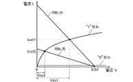
図8は、このようなバイアス関係での選択メモリセルMcellが“1”セルの場合の電圧−電流特性と動作点を、選択NANDストリングがセンスアンプ端から遠い場合(即ちビット線抵抗RBLが大きい場合)と近い場合(即ちビット線抵抗RBLが小さい場合)について実線で示している。負荷直線は、このバイアス関係ではビット線抵抗RBLが選択メモリセルの負荷として見える状態にあることを示している。 FIG. 8 shows the voltage-current characteristics and operating point when the selected memory cell Mcell in such a bias relationship is a “1” cell, when the selected NAND string is far from the sense amplifier end (that is, the bit line resistance RBL is large). )) (Ie, when the bit line resistance RBL is small). The load line indicates that the bit line resistance RBL is visible as a load of the selected memory cell in this bias relationship.
ビット線抵抗RBLが小さい場合、ドレイン・ソース間電圧がVds1でセル電流はIcell1となり、これはほぼメモリセル特性の飽和電流領域の電流である。これに対してビット線抵抗RBLが大きい場合には、選択メモリセルMcellのドレイン・ソース間電圧がVds2でセル電流はIcell2となる。即ちビット線抵抗RBLによって大きくセル電流が制限され、これが誤読み出しの原因となる。 When the bit line resistance RBL is small, the drain-source voltage is Vds1 and the cell current is Icell1, which is almost the current in the saturation current region of the memory cell characteristics. On the other hand, when the bit line resistance RBL is large, the drain-source voltage of the selected memory cell Mcell is Vds2, and the cell current is Icell2. That is, the cell current is largely limited by the bit line resistance RBL, which causes erroneous reading.
より具体的に言えば、選択メモリセルMcellが十分に消去された、負しきい値状態の“1”セルであっても、ビット線抵抗RBLによってメモリセルのドレイン・ソース間電圧が実質的に小さくかつ、セル電流が小さくなる。このため、破線で示した“0”セル(正しきい値の書き込みセル)と誤判定される可能性が生じる。 More specifically, even if the selected memory cell Mcell is sufficiently erased and is a “1” cell in a negative threshold state, the voltage between the drain and source of the memory cell is substantially reduced by the bit line resistance RBL. It is small and the cell current is small. For this reason, there is a possibility of erroneous determination as a “0” cell (positive threshold write cell) indicated by a broken line.
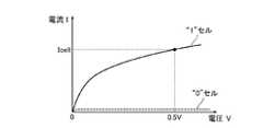
これに対して、図9は、この実施の形態でのセンス方式の場合のセンスアンプSAのクランプ用トランジスタMN1からセルアレイ1内の選択されたNANDストリングNUまでの各部電圧関係を示している。この実施の形態では、センスアンプSA内のクランプ用トランジスタMN1のゲート電圧はトランジスタMN1が十分にオンする電圧、例えば〜4Vとし、代わって選択NANDストリング内のビット線側選択ゲートトランジスタS1のゲートには、0.5V+Vtn(Vtnは、選択ゲートトランジスタのしきい値電圧)を与える。 On the other hand, FIG. 9 shows a voltage relationship between each part from the clamping transistor MN1 of the sense amplifier SA to the selected NAND string NU in the
このようなバイアス関係にすれば、ビット線抵抗RBLの大小により、選択NANDストリングの選択ゲートトランジスタS1のドレイン端電圧が異なるとしても、それが0.5V以上の範囲であれば、選択セルMcellの動作点に影響を与えない。即ちビット線抵抗RBLは選択メモリセルMcellの負荷抵抗としては見えず、選択ゲートトランジスタS1のソース電圧0.5Vがそのまま選択メモリセルMcellのドレインに印加される。 With such a bias relationship, even if the drain terminal voltage of the selection gate transistor S1 of the selected NAND string varies depending on the size of the bit line resistance RBL, if it is in the range of 0.5 V or more, the selected cell Mcell Does not affect the operating point. That is, the bit line resistance RBL does not appear as a load resistance of the selected memory cell Mcell, and the source voltage 0.5 V of the selection gate transistor S1 is applied as it is to the drain of the selected memory cell Mcell.
従って、選択メモリセルが“1”セルの場合のセル特性と動作点は、図10の実線のようになり、そのドレイン・ソース間電圧は、ビット線抵抗によらず、実質的に一定(Vds=0.5V)であり、セル電流Icellも飽和電流領域の十分に大きいほぼ一定電流となる。これにより、ビット線抵抗RBLに起因する誤読み出しを防止することができる。書き込みベリファイ時の誤判定も同様の理由で防止される。 Therefore, the cell characteristic and operating point when the selected memory cell is “1” cell are as shown by the solid line in FIG. 10, and the drain-source voltage is substantially constant (Vds) regardless of the bit line resistance. = 0.5V), and the cell current Icell is also a substantially constant current that is sufficiently large in the saturation current region. Thereby, erroneous reading due to the bit line resistance RBL can be prevented. An erroneous determination at the time of write verification is also prevented for the same reason.
以上のようなセンス動作を可能とするためには、図4に示したSGDドライバ40内の読み出し時用のSGD電圧発生回路41aの変更が必要となる。この点を、図5及び図6を参照して具体的に説明する。 In order to enable the sensing operation as described above, it is necessary to change the SGD
図5は、従来のセンス方式での読み出し用SGD電圧発生回路41aの構成である。Vdd(〜5V)の電源端子と接地端子Vssの間に、基準電流源CS1(基準電流Iref)、ダイオード接続されたNMOSトランジスタM21及び基準抵抗素子R1(基準抵抗Rref)が直列接続されて、基準電圧発生回路51が構成されている。この基準電圧発生回路51により基準電圧Iref×Rrefが得られる。 FIG. 5 shows a configuration of a read SGD
その基準電圧を出力するための電圧出力回路52として、VddとVssの間に、NMOSトランジスタM21とカレントミラーを構成するNMOSトランジスタM22と抵抗素子R2が直列接続されて、ソースフォロアが構成されている。 As a
抵抗素子R1とR2の抵抗値比は、トランジスタM21とM22のチャネル長Lとチャネル幅Wの比L/Wに等しく設定される。例えば、トランジスタM21,M22が同サイズであれば、抵抗R1,R2は同じ抵抗値とする。これにより、出力電圧Iref×Rrefを得ることができ、これが選択ゲートトランジスタのゲート電圧として供給される。 The resistance value ratio of the resistance elements R1 and R2 is set equal to the ratio L / W of the channel length L and the channel width W of the transistors M21 and M22. For example, if the transistors M21 and M22 have the same size, the resistors R1 and R2 have the same resistance value. As a result, the output voltage Iref × Rref can be obtained, and this is supplied as the gate voltage of the selection gate transistor.
これに対し、図6は、この実施の形態のセンス方式での読み出し用SGD電圧発生回路41aの構成である。図5の構成と異なる点は、基準電圧発生回路51に、電流源CS1と抵抗R1との間にダイオード接続した二つのNMOSトランジスタM21,M23を介在させている点、これに対応して、電圧出力回路52にも二つのNMOSトランジスタM22,M24を介在させて、これらのNMOSトランジスタM22,M24の接続ノードを電圧出力ノードとしている点である。 On the other hand, FIG. 6 shows the configuration of the read SGD
NMOSトランジスタM22のゲートは、NMOSトランジスタM21のゲートと共通化され、NMOSトランジスタM24のゲートはNMOSトランジスタM23のゲートと共通化されている。 The gate of the NMOS transistor M22 is shared with the gate of the NMOS transistor M21, and the gate of the NMOS transistor M24 is shared with the gate of the NMOS transistor M23.
このような構成とすることにより、出力電圧は、Iref×Rref+Vtn(VtnはNMOSトランジスタのしきい値電圧)となり、従来方式より高い電圧を選択ゲート線SGDに与えることができる。例えば、Iref=10μA、Rref=50kΩとして、得られる出力電圧は、0.5V+Vtnになる。この出力電圧をより厳密に表現すれば、トランジスタM24のβ値を用いて、Iref×Rref+Vtn+(2Iref/β)1/2となる。With such a configuration, the output voltage becomes Iref × Rref + Vtn (Vtn is the threshold voltage of the NMOS transistor), and a higher voltage than the conventional method can be applied to the selection gate line SGD. For example, when Iref = 10 μA and Rref = 50 kΩ, the output voltage obtained is 0.5 V + Vtn. If this output voltage is expressed more strictly, it becomes Iref × Rref + Vtn + (2Iref / β)1/2 by using the β value of the transistor M24.
実際にメモリセルのドレイン・ソース間電圧は、基準電流Iref又は基準抵抗Rrefにより可変制御することが可能で、セル特性に応じて最適値に設定することができる。また、しきい値電圧Vtnは温度で変化するため、トランジスタM23,M24はメモリコア内部の選択ゲートトランジスタS1の特性と限りなく似ているものが好ましく、例えば同じサイズのトランジスタを用いる。 Actually, the drain-source voltage of the memory cell can be variably controlled by the reference current Iref or the reference resistance Rref, and can be set to an optimum value according to the cell characteristics. Further, since the threshold voltage Vtn changes with temperature, the transistors M23 and M24 are preferably infinitely similar to the characteristics of the select gate transistor S1 in the memory core. For example, transistors of the same size are used.
これらのトランジスタM23,M24により大きなゲート幅Wが必要であれば、図11に示すように、これらをゲート幅の小さいNMOSトランジスタの並列接続により構成すればよい。このゲート幅の小さい単位NMOSトランジスタを、セルアレイ内の選択ゲートトランジスタS1と同じサイズのものとすることにより、トランジスタM23,M24の特性を選択ゲートトランジスタS1と揃えることができる。 If a large gate width W is required for these transistors M23 and M24, these may be configured by parallel connection of NMOS transistors having a small gate width as shown in FIG. By making the unit NMOS transistor having a small gate width the same size as the selection gate transistor S1 in the cell array, the characteristics of the transistors M23 and M24 can be matched with those of the selection gate transistor S1.
1…メモリセルアレイ、2…ロウデコーダ、3…センスアンプ回路、4…コアコントロールドライバ、5…カラムデコーダ、6…アドレスレジスタ、7…高電圧発生回路、8…コントロール回路、9…I/Oバッファ、40…選択ゲート線(SGD)ドライバ、41a−41e…SGD電圧発生回路、51…基準電圧発生回路、52…電圧出力回路、MU…NANDストリング、M0−M31…メモリセル、S1,S2…選択ゲートトランジスタ、CS1…電流源、R1,R2…抵抗素子、M21,M22,M32,M24…NMOSトランジスタ。DESCRIPTION OF
Claims (5)
Translated fromJapanese前記ビット線に電流を供給するための電流源を備えて、前記メモリセルのセル電流によってそのセルデータを検知するセンスアンプと、
読み出し時、前記メモリセルのドレイン・ソース間電圧を前記ビット線の抵抗によらず実質的に一定に保つように、前記選択ゲートトランジスタのゲートを駆動する選択ゲート線ドライバと、
を有することを特徴とする半導体記憶装置。A memory cell connected to a bit line via a select gate transistor;
A sense amplifier that includes a current source for supplying current to the bit line, and that senses cell data based on a cell current of the memory cell;
A selection gate line driver that drives the gate of the selection gate transistor so that the drain-source voltage of the memory cell is kept substantially constant regardless of the resistance of the bit line at the time of reading;
A semiconductor memory device comprising:
ことを特徴とする請求項1記載の半導体記憶装置。2. The semiconductor memory device according to claim 1, wherein a plurality of memory cells are connected in series to form a NAND string, and one end thereof is connected to the bit line via the selection gate transistor.
電源端子と接地端子の間に基準電流源、ダイオード接続された第1及び第2のNMOSトランジスタ、及び第1の抵抗素子が直列接続された基準電圧発生回路と、
電源端子と接地端子の間に前記第1及び第2のNMOSトランジスタとそれぞれゲートが共通接続された第3及び第4のNMOSトランジスタと第2の抵抗素子とが直列接続されて、前記第3及び第4のNMOSトランジスタの接続ノードが前記選択ゲートトランジスタのゲートに供給される電圧出力ノードとなる電圧出力回路とを有する
ことを特徴とする請求項1記載の半導体記憶装置。The selection gate line driver is:
A reference voltage generation circuit in which a reference current source, a diode-connected first and second NMOS transistors, and a first resistance element are connected in series between a power supply terminal and a ground terminal;
Between the power supply terminal and the ground terminal, the first and second NMOS transistors and the third and fourth NMOS transistors having the gates connected in common and the second resistance element are connected in series, and the third and 2. The semiconductor memory device according to claim 1, further comprising: a voltage output circuit in which a connection node of the fourth NMOS transistor is a voltage output node supplied to a gate of the selection gate transistor.
ことを特徴とする請求項3記載の半導体記憶装置。The channel length / channel width ratio of the first NMOS transistor and the third NMOS transistor is set to be equal to a resistance value ratio of the first resistance element and the second resistance element. Item 4. The semiconductor memory device according to Item 3.
ことを特徴とする請求項3記載の半導体記憶装置。4. The semiconductor memory device according to claim 3, wherein each of the third and fourth NMOS transistors is constituted by a parallel connection of a plurality of transistors having the same size as the selection gate transistor.
Priority Applications (2)
| Application Number | Priority Date | Filing Date | Title |
|---|---|---|---|
| JP2008146611AJP2009295221A (en) | 2008-06-04 | 2008-06-04 | Semiconductor memory device |
| US12/413,065US20090303796A1 (en) | 2008-06-04 | 2009-03-27 | Semiconductor memory device |
Applications Claiming Priority (1)
| Application Number | Priority Date | Filing Date | Title |
|---|---|---|---|
| JP2008146611AJP2009295221A (en) | 2008-06-04 | 2008-06-04 | Semiconductor memory device |
Publications (1)
| Publication Number | Publication Date |
|---|---|
| JP2009295221Atrue JP2009295221A (en) | 2009-12-17 |
Family
ID=41400184
Family Applications (1)
| Application Number | Title | Priority Date | Filing Date |
|---|---|---|---|
| JP2008146611AWithdrawnJP2009295221A (en) | 2008-06-04 | 2008-06-04 | Semiconductor memory device |
Country Status (2)
| Country | Link |
|---|---|
| US (1) | US20090303796A1 (en) |
| JP (1) | JP2009295221A (en) |
Cited By (2)
| Publication number | Priority date | Publication date | Assignee | Title |
|---|---|---|---|---|
| WO2011078414A2 (en) | 2009-12-25 | 2011-06-30 | Asahi Glass Company, Limited. | Substrate for euvl optical member |
| JP2017073183A (en)* | 2015-10-05 | 2017-04-13 | 力晶科技股▲ふん▼有限公司 | Sense circuit for nonvolatile memory device and nonvolatile memory device |
Families Citing this family (3)
| Publication number | Priority date | Publication date | Assignee | Title |
|---|---|---|---|---|
| US9672941B1 (en) | 2016-02-08 | 2017-06-06 | Infineon Technologies Ag | Memory element status detection |
| KR102444947B1 (en)* | 2016-03-31 | 2022-09-21 | 에스케이하이닉스 주식회사 | Semiconductor device |
| JP2018156697A (en)* | 2017-03-15 | 2018-10-04 | 東芝メモリ株式会社 | Semiconductor memory device |
Family Cites Families (15)
| Publication number | Priority date | Publication date | Assignee | Title |
|---|---|---|---|---|
| US4694429A (en)* | 1984-11-29 | 1987-09-15 | Kabushiki Kaisha Toshiba | Semiconductor memory device |
| JP2790495B2 (en)* | 1989-11-02 | 1998-08-27 | 沖電気工業株式会社 | Nonvolatile semiconductor memory device |
| US5726934A (en)* | 1996-04-09 | 1998-03-10 | Information Storage Devices, Inc. | Method and apparatus for analog reading values stored in floating gate structures |
| JP2001184881A (en)* | 1999-12-28 | 2001-07-06 | Toshiba Corp | Readout circuit for nonvolatile semiconductor memory |
| ITRM20010001A1 (en)* | 2001-01-03 | 2002-07-03 | Micron Technology Inc | LOW VOLTAGE FLASH MEMORY DETECTION CIRCUIT. |
| US6907497B2 (en)* | 2001-12-20 | 2005-06-14 | Kabushiki Kaisha Toshiba | Non-volatile semiconductor memory device |
| US7196931B2 (en)* | 2002-09-24 | 2007-03-27 | Sandisk Corporation | Non-volatile memory and method with reduced source line bias errors |
| US7443757B2 (en)* | 2002-09-24 | 2008-10-28 | Sandisk Corporation | Non-volatile memory and method with reduced bit line crosstalk errors |
| JP4287235B2 (en)* | 2003-10-09 | 2009-07-01 | 株式会社東芝 | Nonvolatile semiconductor memory device |
| KR100706826B1 (en)* | 2005-09-08 | 2007-04-12 | 주식회사 하이닉스반도체 | Bitline Precharge Voltage Generator |
| JP4901204B2 (en)* | 2005-12-13 | 2012-03-21 | 株式会社東芝 | Semiconductor integrated circuit device |
| US7733704B2 (en)* | 2005-12-29 | 2010-06-08 | Sandisk Corporation | Non-volatile memory with power-saving multi-pass sensing |
| US7663932B2 (en)* | 2007-12-27 | 2010-02-16 | Kabushiki Kaisha Toshiba | Nonvolatile semiconductor memory device |
| JP5127439B2 (en)* | 2007-12-28 | 2013-01-23 | 株式会社東芝 | Semiconductor memory device |
| JP4635066B2 (en)* | 2008-03-19 | 2011-02-16 | 株式会社東芝 | Semiconductor memory device |
- 2008
- 2008-06-04JPJP2008146611Apatent/JP2009295221A/ennot_activeWithdrawn
- 2009
- 2009-03-27USUS12/413,065patent/US20090303796A1/ennot_activeAbandoned
Cited By (2)
| Publication number | Priority date | Publication date | Assignee | Title |
|---|---|---|---|---|
| WO2011078414A2 (en) | 2009-12-25 | 2011-06-30 | Asahi Glass Company, Limited. | Substrate for euvl optical member |
| JP2017073183A (en)* | 2015-10-05 | 2017-04-13 | 力晶科技股▲ふん▼有限公司 | Sense circuit for nonvolatile memory device and nonvolatile memory device |
Also Published As
| Publication number | Publication date |
|---|---|
| US20090303796A1 (en) | 2009-12-10 |
Similar Documents
| Publication | Publication Date | Title |
|---|---|---|
| JP3653449B2 (en) | Nonvolatile semiconductor memory device | |
| KR0184093B1 (en) | Non-volatile semiconductor memory device and data erasing method therefor | |
| JP4856138B2 (en) | Nonvolatile semiconductor memory device | |
| KR100829790B1 (en) | Flash memory device and data reading method of flash memory device | |
| JP3833970B2 (en) | Nonvolatile semiconductor memory | |
| KR100781984B1 (en) | Sense Amplifier Circuit with Self-Reference and Sensing Method Thereby | |
| US20050036369A1 (en) | Temperature compensated bit-line precharge | |
| US8351274B2 (en) | Semiconductor memory device and method of precharging the same with a first and second precharge voltage simultaneously applied to a bit line | |
| JP2001332093A (en) | Non-volatile semiconductor memory | |
| US10332593B2 (en) | Semiconductor memory device configured to sense memory cell threshold voltages in ascending order | |
| JP3920943B2 (en) | Nonvolatile semiconductor memory device | |
| JP2013232258A (en) | Semiconductor memory device | |
| JP2009043390A (en) | Soft program method in non-volatile memory device | |
| US7796441B2 (en) | Method of reading configuration data in flash memory device | |
| JP2009301607A (en) | Nonvolatile semiconductor memory device and method for controlling the same | |
| JP2007193854A (en) | Semiconductor memory device | |
| JP4855773B2 (en) | Semiconductor memory device and data read method thereof | |
| JP2009295221A (en) | Semiconductor memory device | |
| JP2010129125A (en) | Multivalue nonvolatile semiconductor memory | |
| JP2011159355A (en) | Semiconductor memory device | |
| JP4960078B2 (en) | Nonvolatile semiconductor memory device | |
| US8509019B2 (en) | Voltage generation circuit and nonvolatile memory device including the same | |
| US7889559B2 (en) | Circuit for generating a voltage and a non-volatile memory device having the same | |
| CN101414484A (en) | Non-volatile memory device | |
| US20140269096A1 (en) | Non-volatile semiconductor memory device and method of programming the same |
Legal Events
| Date | Code | Title | Description |
|---|---|---|---|
| A300 | Application deemed to be withdrawn because no request for examination was validly filed | Free format text:JAPANESE INTERMEDIATE CODE: A300 Effective date:20110906 |