JP2009294376A - Image display apparatus - Google Patents
Image display apparatusDownload PDFInfo
- Publication number
- JP2009294376A JP2009294376AJP2008147016AJP2008147016AJP2009294376AJP 2009294376 AJP2009294376 AJP 2009294376AJP 2008147016 AJP2008147016 AJP 2008147016AJP 2008147016 AJP2008147016 AJP 2008147016AJP 2009294376 AJP2009294376 AJP 2009294376A
- Authority
- JP
- Japan
- Prior art keywords
- voltage
- transistor
- self
- gate electrode
- electrode
- Prior art date
- Legal status (The legal status is an assumption and is not a legal conclusion. Google has not performed a legal analysis and makes no representation as to the accuracy of the status listed.)
- Pending
Links
Images


Classifications
- G—PHYSICS
- G09—EDUCATION; CRYPTOGRAPHY; DISPLAY; ADVERTISING; SEALS
- G09G—ARRANGEMENTS OR CIRCUITS FOR CONTROL OF INDICATING DEVICES USING STATIC MEANS TO PRESENT VARIABLE INFORMATION
- G09G3/00—Control arrangements or circuits, of interest only in connection with visual indicators other than cathode-ray tubes
- G09G3/20—Control arrangements or circuits, of interest only in connection with visual indicators other than cathode-ray tubes for presentation of an assembly of a number of characters, e.g. a page, by composing the assembly by combination of individual elements arranged in a matrix no fixed position being assigned to or needed to be assigned to the individual characters or partial characters
- G09G3/22—Control arrangements or circuits, of interest only in connection with visual indicators other than cathode-ray tubes for presentation of an assembly of a number of characters, e.g. a page, by composing the assembly by combination of individual elements arranged in a matrix no fixed position being assigned to or needed to be assigned to the individual characters or partial characters using controlled light sources
- G09G3/30—Control arrangements or circuits, of interest only in connection with visual indicators other than cathode-ray tubes for presentation of an assembly of a number of characters, e.g. a page, by composing the assembly by combination of individual elements arranged in a matrix no fixed position being assigned to or needed to be assigned to the individual characters or partial characters using controlled light sources using electroluminescent panels
- G09G3/32—Control arrangements or circuits, of interest only in connection with visual indicators other than cathode-ray tubes for presentation of an assembly of a number of characters, e.g. a page, by composing the assembly by combination of individual elements arranged in a matrix no fixed position being assigned to or needed to be assigned to the individual characters or partial characters using controlled light sources using electroluminescent panels semiconductive, e.g. using light-emitting diodes [LED]
- G09G3/3208—Control arrangements or circuits, of interest only in connection with visual indicators other than cathode-ray tubes for presentation of an assembly of a number of characters, e.g. a page, by composing the assembly by combination of individual elements arranged in a matrix no fixed position being assigned to or needed to be assigned to the individual characters or partial characters using controlled light sources using electroluminescent panels semiconductive, e.g. using light-emitting diodes [LED] organic, e.g. using organic light-emitting diodes [OLED]
- G09G3/3225—Control arrangements or circuits, of interest only in connection with visual indicators other than cathode-ray tubes for presentation of an assembly of a number of characters, e.g. a page, by composing the assembly by combination of individual elements arranged in a matrix no fixed position being assigned to or needed to be assigned to the individual characters or partial characters using controlled light sources using electroluminescent panels semiconductive, e.g. using light-emitting diodes [LED] organic, e.g. using organic light-emitting diodes [OLED] using an active matrix
- G09G3/3233—Control arrangements or circuits, of interest only in connection with visual indicators other than cathode-ray tubes for presentation of an assembly of a number of characters, e.g. a page, by composing the assembly by combination of individual elements arranged in a matrix no fixed position being assigned to or needed to be assigned to the individual characters or partial characters using controlled light sources using electroluminescent panels semiconductive, e.g. using light-emitting diodes [LED] organic, e.g. using organic light-emitting diodes [OLED] using an active matrix with pixel circuitry controlling the current through the light-emitting element
- G—PHYSICS
- G09—EDUCATION; CRYPTOGRAPHY; DISPLAY; ADVERTISING; SEALS
- G09G—ARRANGEMENTS OR CIRCUITS FOR CONTROL OF INDICATING DEVICES USING STATIC MEANS TO PRESENT VARIABLE INFORMATION
- G09G2300/00—Aspects of the constitution of display devices
- G09G2300/04—Structural and physical details of display devices
- G09G2300/0421—Structural details of the set of electrodes
- G09G2300/043—Compensation electrodes or other additional electrodes in matrix displays related to distortions or compensation signals, e.g. for modifying TFT threshold voltage in column driver
- G—PHYSICS
- G09—EDUCATION; CRYPTOGRAPHY; DISPLAY; ADVERTISING; SEALS
- G09G—ARRANGEMENTS OR CIRCUITS FOR CONTROL OF INDICATING DEVICES USING STATIC MEANS TO PRESENT VARIABLE INFORMATION
- G09G2300/00—Aspects of the constitution of display devices
- G09G2300/08—Active matrix structure, i.e. with use of active elements, inclusive of non-linear two terminal elements, in the pixels together with light emitting or modulating elements
- G09G2300/0809—Several active elements per pixel in active matrix panels
- G09G2300/0814—Several active elements per pixel in active matrix panels used for selection purposes, e.g. logical AND for partial update
- G—PHYSICS
- G09—EDUCATION; CRYPTOGRAPHY; DISPLAY; ADVERTISING; SEALS
- G09G—ARRANGEMENTS OR CIRCUITS FOR CONTROL OF INDICATING DEVICES USING STATIC MEANS TO PRESENT VARIABLE INFORMATION
- G09G2300/00—Aspects of the constitution of display devices
- G09G2300/08—Active matrix structure, i.e. with use of active elements, inclusive of non-linear two terminal elements, in the pixels together with light emitting or modulating elements
- G09G2300/0809—Several active elements per pixel in active matrix panels
- G09G2300/0819—Several active elements per pixel in active matrix panels used for counteracting undesired variations, e.g. feedback or autozeroing
- G—PHYSICS
- G09—EDUCATION; CRYPTOGRAPHY; DISPLAY; ADVERTISING; SEALS
- G09G—ARRANGEMENTS OR CIRCUITS FOR CONTROL OF INDICATING DEVICES USING STATIC MEANS TO PRESENT VARIABLE INFORMATION
- G09G2320/00—Control of display operating conditions
- G09G2320/04—Maintaining the quality of display appearance
- G09G2320/043—Preventing or counteracting the effects of ageing
- G09G2320/045—Compensation of drifts in the characteristics of light emitting or modulating elements
- G—PHYSICS
- G09—EDUCATION; CRYPTOGRAPHY; DISPLAY; ADVERTISING; SEALS
- G09G—ARRANGEMENTS OR CIRCUITS FOR CONTROL OF INDICATING DEVICES USING STATIC MEANS TO PRESENT VARIABLE INFORMATION
- G09G2320/00—Control of display operating conditions
- G09G2320/04—Maintaining the quality of display appearance
- G09G2320/043—Preventing or counteracting the effects of ageing
- G09G2320/046—Dealing with screen burn-in prevention or compensation of the effects thereof
- G—PHYSICS
- G09—EDUCATION; CRYPTOGRAPHY; DISPLAY; ADVERTISING; SEALS
- G09G—ARRANGEMENTS OR CIRCUITS FOR CONTROL OF INDICATING DEVICES USING STATIC MEANS TO PRESENT VARIABLE INFORMATION
- G09G3/00—Control arrangements or circuits, of interest only in connection with visual indicators other than cathode-ray tubes
- G09G3/20—Control arrangements or circuits, of interest only in connection with visual indicators other than cathode-ray tubes for presentation of an assembly of a number of characters, e.g. a page, by composing the assembly by combination of individual elements arranged in a matrix no fixed position being assigned to or needed to be assigned to the individual characters or partial characters
- G09G3/22—Control arrangements or circuits, of interest only in connection with visual indicators other than cathode-ray tubes for presentation of an assembly of a number of characters, e.g. a page, by composing the assembly by combination of individual elements arranged in a matrix no fixed position being assigned to or needed to be assigned to the individual characters or partial characters using controlled light sources
- G09G3/30—Control arrangements or circuits, of interest only in connection with visual indicators other than cathode-ray tubes for presentation of an assembly of a number of characters, e.g. a page, by composing the assembly by combination of individual elements arranged in a matrix no fixed position being assigned to or needed to be assigned to the individual characters or partial characters using controlled light sources using electroluminescent panels
- G09G3/32—Control arrangements or circuits, of interest only in connection with visual indicators other than cathode-ray tubes for presentation of an assembly of a number of characters, e.g. a page, by composing the assembly by combination of individual elements arranged in a matrix no fixed position being assigned to or needed to be assigned to the individual characters or partial characters using controlled light sources using electroluminescent panels semiconductive, e.g. using light-emitting diodes [LED]
- G09G3/3208—Control arrangements or circuits, of interest only in connection with visual indicators other than cathode-ray tubes for presentation of an assembly of a number of characters, e.g. a page, by composing the assembly by combination of individual elements arranged in a matrix no fixed position being assigned to or needed to be assigned to the individual characters or partial characters using controlled light sources using electroluminescent panels semiconductive, e.g. using light-emitting diodes [LED] organic, e.g. using organic light-emitting diodes [OLED]
- G09G3/3275—Details of drivers for data electrodes
Landscapes
- Engineering & Computer Science (AREA)
- Physics & Mathematics (AREA)
- Computer Hardware Design (AREA)
- General Physics & Mathematics (AREA)
- Theoretical Computer Science (AREA)
- Control Of Indicators Other Than Cathode Ray Tubes (AREA)
- Control Of El Displays (AREA)
- Electroluminescent Light Sources (AREA)
Abstract
Translated fromJapaneseDescription
Translated fromJapanese本発明は、画像表示装置に係り、特に、アクティブマトリクス方式の有機エレクトロルミネッセンスディスプレイに関する。 The present invention relates to an image display device, and more particularly to an active matrix organic electroluminescence display.
アクティブマトリクス駆動の有機エレクトロルミネッセンスディスプレイパネル(以下、有機EL表示パネルという。)を有する有機エレクトロルミネッセンスディスプレイ(以下、有機EL表示装置という。)は、次世代のフラットパネルディスプレイとして期待されている。
有機EL表示パネルは、有機エレクトロルミネッセンス素子(以下、有機EL素子という。)と、有機EL素子に電流を供給するための駆動用の薄膜トランジスタ(以下、EL駆動TFTという。)を有するのが普通である。
一方、有機EL素子は、定電流を印加すると、図13に示すように、時間(図13のT)の経過とともに、輝度(図13のBr)が下がっていき、それに伴い、有機EL素子のアノード電圧(図13のVoled)が上昇していく。図14に示すように、この輝度の劣化率(図14のbrate)とアノード電圧(図14のVoled)の上昇値(図14のVdeg)は線形の関係にある。
ここで、図15に示すような白い四角形を表示した場合、黒表示部に対して、白い四角形の表示部の劣化が早いため、隣接画素における輝度差が生じ、この輝度が1%を超えた時、図15のAに示すように、「焼き付き」として確認される。
ここで、有機EL表示パネルで焼き付が生じた部分を含む1表示ライン(Yアドレス)上のXアドレス(図16のXadres)の有機EL素子のアノード電圧(図16のVoled)をスキャンしていくと、図16に示すような図となる。なお、図16のAが「焼き付き」の始まりの点、図16のBの領域が正常領域、図16のCの領域が、焼き付きが生じて劣化した領域を示す。
この焼き付きを防止するための技術が、下記特許文献1〜特許文献3に開示されている。
前述の特許文献1、特許文献2に記載されている技術は、有機EL素子が焼付きのない安定した発光をするために、電流計測によって得られた測定結果をA/D変換し、得られたデジタルデータを基に、有機EL素子の駆動電圧にフィードバックを行うものである。
また、前述の特許文献3に記載されている技術は、有機EL素子の端子電圧を測定し、規定値と比較することにより、有機EL素子の駆動電圧を補正するものであり、予め記録しておいた有機EL素子の端子電圧と電流の関係から駆動電流を補正するものである。An organic electroluminescence display (hereinafter referred to as an organic EL display device) having an organic electroluminescence display panel driven by an active matrix (hereinafter referred to as an organic EL display panel) is expected as a next-generation flat panel display.
An organic EL display panel usually has an organic electroluminescence element (hereinafter referred to as an organic EL element) and a driving thin film transistor (hereinafter referred to as an EL driving TFT) for supplying a current to the organic EL element. is there.
On the other hand, when a constant current is applied to the organic EL element, the luminance (Br in FIG. 13) decreases with the passage of time (T in FIG. 13) as shown in FIG. The anode voltage (Voled in FIG. 13) increases. As shown in FIG. 14, the luminance deterioration rate (brate in FIG. 14) and the increase value (Vdeg in FIG. 14) of the anode voltage (Voled in FIG. 14) have a linear relationship.
Here, when a white square as shown in FIG. 15 is displayed, since the white square display portion deteriorates faster than the black display portion, a luminance difference occurs between adjacent pixels, and this luminance exceeds 1%. At this time, it is confirmed as “burn-in” as shown in FIG.
Here, the anode voltage (Voled in FIG. 16) of the organic EL element at the X address (Xadres in FIG. 16) on one display line (Y address) including the portion where burn-in occurs in the organic EL display panel is scanned. Then, a diagram as shown in FIG. 16 is obtained. 16A indicates the start point of “burn-in”, the region B in FIG. 16 indicates a normal region, and the region C in FIG. 16 indicates a region deteriorated due to burn-in.
Techniques for preventing this burn-in are disclosed in the following
The techniques described in
Further, the technique described in
なお、本願発明に関連する先行技術文献としては以下のものがある。
しかしながら、前述の特許文献1〜特許文献3に記載されている技術は、以下のような問題点があった。
(1)前述の特許文献1、特許文献2に記載されている技術では、有機EL素子からEL駆動TFTへフィードバックする信号に関する具体的な記載がなく、補正信号をどう生成するか分からないため、検出動作が正確にできたとしても正確な補正ができるとは限らない。
(2)前述の特許文献3に記載されている技術では、予め記録しておいた有機EL素子の端子電圧と電流の関係から駆動電流を補正するため、補正のための膨大なデータテーブルを必要とする。
本発明は、前記従来技術の問題点を解決するためになされたものであり、本発明の目的は、画像表示装置において、自発光素子の劣化に対して正確な補正を行うことができる技術を提供することにある。
本発明の前記ならびにその他の目的と新規な特徴は、本明細書の記述及び添付図面によって明らかにする。However, the techniques described in
(1) In the techniques described in
(2) In the technique described in
The present invention has been made to solve the above-described problems of the prior art, and an object of the present invention is to provide a technique capable of accurately correcting the deterioration of the self-luminous element in the image display device. It is to provide.
The above and other objects and novel features of the present invention will become apparent from the description of this specification and the accompanying drawings.
本願において開示される発明のうち、代表的なものの概要を簡単に説明すれば、下記の通りである。
本発明は、それぞれ自発光素子と、前記自発光素子を駆動する駆動トランジスタとを有する複数の画素と、前記画素に画像電圧を入力する複数の信号線とを備え、前記駆動トランジスタは、飽和領域で駆動される画像表示装置であって、前記画素の前記自発光素子に定電流を供給したときの前記各画素の前記自発光素子の両端の電圧を検出する電圧検出手段と、前記電圧検出手段で検出した電圧が閾値電圧を越えた場合に、リファレンス電圧、あるいは電源電圧を制御し、前記複数の画素の全ての画素の前記駆動トランジスタの動作領域を飽和領域に保つ手段とを有する
また、本発明では、隣接した前記画素の前記自発光素子の特性差を検出する検出手段と、前記検出手段により劣化と判断された画素の前記自発光素子に対して、リファレンス電圧と画像電圧との差分の電圧を演算する手段1と、前記手段1での演算結果に非線形の発光の補正量を掛算する手段2と、前記リファレンス電圧から前記手段2での演算結果を減算して補正後の画像電圧を演算する手段3とを有する。Of the inventions disclosed in this application, the outline of typical ones will be briefly described as follows.
The present invention includes a plurality of pixels each having a self-luminous element and a driving transistor for driving the self-luminous element, and a plurality of signal lines for inputting an image voltage to the pixel. An image display device driven by a voltage detecting means for detecting a voltage across the self light emitting element of each pixel when a constant current is supplied to the self light emitting element of the pixel; and the voltage detecting means And a means for controlling the reference voltage or the power supply voltage when the voltage detected in step (b) exceeds the threshold voltage, and maintaining the operation region of the drive transistor of all the pixels of the plurality of pixels in a saturation region. In the present invention, a detection unit that detects a difference in characteristics of the self-light-emitting elements of the adjacent pixels, and a reference for the self-light-emitting elements of the pixels that are determined to be deteriorated by the detection unit. Means 1 for calculating the difference voltage between the scan voltage and the image voltage, means 2 for multiplying the calculation result of the
また、前記検出手段は、定電流供給手段と、検出期間内に、前記定電流供給手段から前記各画素の前記自発光素子に定電流を供給したときの前記各画素の前記自発光素子の両端の電圧を検出する電圧検出手段と、前記電圧検出手段で検出した電圧をデジタル値に変換するAD変換手段と、前記AD変換手段で変換されたデジタル値を記憶するメモリと、前記メモリに記憶されたデジタル値に基づき、前記隣接した前記画素の前記自発光素子の特性差を検出し、前記劣化した前記自発光素子を判定する判定手段とを有する。
また、本発明では、前記判定手段において、前記自発光素子の発光輝度の劣化量がα%と判定された場合、前記発光の補正量は、非線形の√[1/{1−(α/100)}]である。
また、本発明では、前記手段1は、リファレンス電圧と画像電圧の差分の電圧を出力する第1減算回路であり、前記手段2は、前記判定手段の判定結果に基づき前記第1減算回路の出力を利得√[1/{1−(α/100)}]で増幅する増幅器であり、前記手段3は、前記リファレンス電圧と前記増幅器の出力の差分の電圧を出力する第2減算回路である。
また、本発明では、前記自発光素子は、有機発光ダイオード素子である。The detection means includes a constant current supply means and both ends of the self light emitting element of each pixel when a constant current is supplied from the constant current supply means to the self light emitting element of each pixel within the detection period. Voltage detecting means for detecting the voltage of the AD, AD converting means for converting the voltage detected by the voltage detecting means into a digital value, a memory for storing the digital value converted by the AD converting means, and stored in the memory Determining means for detecting a characteristic difference between the self-light-emitting elements of the adjacent pixels based on the digital value and determining the degraded self-light-emitting element.
In the present invention, when the determination means determines that the deterioration amount of the light emission luminance of the self-luminous element is α%, the correction amount of the light emission is nonlinear √ [1 // (1- (α / 100). )}].
In the present invention, the
In the present invention, the self-luminous element is an organic light-emitting diode element.
本願において開示される発明のうち代表的なものによって得られる効果を簡単に説明すれば、下記の通りである。
本発明の画像表示装置によれば、自発光素子の劣化に対して正確な補正を行うことが可能となる。The effects obtained by the representative ones of the inventions disclosed in the present application will be briefly described as follows.
According to the image display device of the present invention, it is possible to perform accurate correction for the deterioration of the self-luminous element.
以下、図面を参照して本発明の実施例を詳細に説明する。
なお、実施例を説明するための全図において、同一機能を有するものは同一符号を付け、その繰り返しの説明は省略する。
[実施例1]
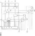
図1は、本発明の実施例1の焼き付き検出と補正機能を内蔵した有機EL表示パネルの概略構成を示す図である。
本実施例では、図1に示すように、先ず、特性検出部14内の電流源20から各有機EL素子に一定の電流を流し、その時の有機EL素子のアノード電圧を、バッファ回路21とローパスフィルタ22を介して検出し、コンパレータ27において閾値電圧と比較する。
検出した電圧が閾値電圧を超えている場合に、表示画素全体に共通の電圧を印加するリファレンス電圧(Vref)や電源電圧(Vdd)を制御して、焼き付けを防止する。
なお、図1において、10は電源回路、12は表示用走査回路、13は検出用走査回路、15は外部電圧制御部、70は表示画素、78は信号線、79は電源線、91は検出制御線、100は制御信号線群、Vextは外部電圧である。
スイッチ(SWA)は、「書込み期間」に、信号線78を、信号駆動回路11の対応する出力端子に接続し、スイッチ(SWB)は、「検出期間」に、信号線78を、特性検出部14内の電流源20に接続する。さらに、外部電圧制御部15は、「発光期間」に、信号線78を、外部電源(例えば、三角波電圧、あるいは、鋸歯状歯電圧)(Vext)に接続する。
また、表示画素70、信号駆動回路11、表示用走査回路12、検出用走査回路13等の各回路は全て、一般に良く知られている低温多結晶シリコン薄膜を用いてガラス基板上に構成されている。また、実際には表示画素70は、有機EL表示パネルの表示領域AR内に多数個配置される。Hereinafter, embodiments of the present invention will be described in detail with reference to the drawings.
In all the drawings for explaining the embodiments, parts having the same functions are given the same reference numerals, and repeated explanation thereof is omitted.
[Example 1]
FIG. 1 is a diagram showing a schematic configuration of an organic EL display panel incorporating a burn-in detection and correction function according to the first embodiment of the present invention.
In this embodiment, as shown in FIG. 1, first, a constant current is supplied from the
When the detected voltage exceeds the threshold voltage, the reference voltage (Vref) and the power supply voltage (Vdd) for applying a common voltage to the entire display pixel are controlled to prevent burning.
In FIG. 1, 10 is a power supply circuit, 12 is a display scanning circuit, 13 is a detection scanning circuit, 15 is an external voltage control unit, 70 is a display pixel, 78 is a signal line, 79 is a power supply line, and 91 is a detection. A control line, 100 is a control signal line group, and Vext is an external voltage.
The switch (SWA) connects the
Further, each circuit such as the
図1に示すように、有機EL表示パネルの表示領域AR内には複数の表示画素70がマトリクス状に設けられる。
図2は、図1に示す有機EL表示パネル内の表示画素の一例を示す等価回路である。なお、図2に示す表示画素の場合、図1に示す制御信号線群100は、セレクト制御線71、点灯スイッチ線75で構成される。セレクト制御線71と、点灯スイッチ線75は、表示用走査回路12に接続される。また、検出制御線91は、検出用走査回路13に接続される。
各表示画素70は、発光素子としての有機エレクトロルミネッセンス素子(以下、有機EL素子という。)1を有しており、有機EL素子1のカソード電極は共通接地線に接続される。また、アノード電極は、点灯用のn型薄膜トランジスタ(以下、点灯TFTスイッチという。)731と、p型薄膜トランジスタ(以下、駆動TFTという。)72を介して電源線79に接続される。電源線79は電源回路10に接続される。
また、駆動TFT72のゲート電極は、保持容量74を介して信号線78に接続され、駆動TFT72のドレイン電極とゲート電極との間には、リセット用のn型薄膜トランジスタ(以下、セレクトスイッチという。)76が設けられる。なお、セレクトスイッチ76のゲート電極は、セレクト制御線71に接続される。また、点灯TFTスイッチ731のゲート電極は、点灯スイッチ線75に接続される。
また、有機EL素子1のアノード電極と信号線78との間に、有機EL素子1の端子間電圧検出用の薄膜トランジスタ(以下、検出スイッチという。)90が接続され、この検出スイッチ90のゲート電極は、検出制御線91に接続される。
なお、駆動TFT72、点灯TFTスイッチ731、セレクトスイッチ76、および検出スイッチ90は、それぞれ半導体層にポリシリコンを用いる多結晶シリコン薄膜トランジスタを用いてガラス基板上に構成されている。なお、多結晶シリコン薄膜トランジスタ、あるいは、有機EL素子1の製造方法などに関しては、一般に報告されているものと大きな相違はないため、ここではその説明は省略する。As shown in FIG. 1, a plurality of
FIG. 2 is an equivalent circuit showing an example of display pixels in the organic EL display panel shown in FIG. In the case of the display pixel shown in FIG. 2, the control
Each
The gate electrode of the
A thin film transistor (hereinafter referred to as a detection switch) 90 for detecting a voltage between terminals of the
The driving
図2に示す表示画素70を有する有機EL表示パネルの場合、予め1/60秒に設定されている1フレーム期間は、例えば、「書込み期間」と「発光期間」と「検出期間」とに3分割されている。
図2に示す表示画素70を有する有機EL表示パネルの駆動方法は良く知られているのでここではその説明は省略する。
但し、図2に示す表示画素70を有する有機EL表示パネルの場合、図3に示すように、「検出期間」では、検出制御線91Aないし検出制御線91Nが順次オンとなり、各検出制御線がオンの期間に、スイッチ(SWB1)からスイッチ(SWBn)が順次オンとなる。
これにより、各有機EL素子1には、順次、特性検出部14内の電流源20から定電流が流れ、特性検出部14において、各有機EL素子1のアノード電圧が検出される。
なお、図4に示すように、「検出期間」は、1フレーム(FLA)内のブランキング期間(BRK)に行うようにしてもよい。
図4では、各ブランキング期間(BRK)毎に、検出制御線91Aないし検出制御線91Nが順次オンとなり、各検出制御線がオンの期間に、スイッチ(SWB1)からスイッチ(SWBn)が順次オンとなる。したがって、図4の場合は、各ブランキング期間(BRK)毎に、1表示ライン上の有機EL素子1が検査される。In the case of the organic EL display panel having the
Since the driving method of the organic EL display panel having the
However, in the case of the organic EL display panel having the
Thereby, a constant current flows sequentially from each
As shown in FIG. 4, the “detection period” may be performed during a blanking period (BRK) within one frame (FLA).
In FIG. 4, the
図5は、図1に示す有機EL表示パネル内の表示画素の他の例を示す等価回路である。
なお、図5に示す表示画素の場合、図1に示す制御信号線群100は、点灯スイッチ線75、リセット線83、セレクトスイッチ線85で構成される。点灯スイッチ線75、リセット線83、セレクトスイッチ線85は、表示用走査回路12に接続される。また、検出制御線91は、検出用走査回路13に接続される。
各表示画素70は、有機EL素子1を有しており、有機EL素子1のカソード電極は共通接地線に接続される。また、アノード電極は、点灯用のp型薄膜トランジスタ(以下、点灯TFTスイッチという。)732と、p型薄膜トランジスタ(以下、駆動TFTという。)72を介して電源線79に接続される。電源線79は電源回路10に接続される。
また、駆動TFT72のソース電極とゲート電極との間には、第1の保持容量80が接続され、さらに、駆動TFT72のゲート電極は、第2の保持容量81とp型薄膜トランジスタ(以下、セレクトスイッチという。)84を介して信号線78に接続される。
駆動TFT72のドレイン電極とゲート電極との間には、リセット用のn型薄膜トランジスタ(以下、リセットTFTスイッチという。)82が設けられる。なお、セレクトスイッチ84のゲート電極は、セレクトスイッチ線85に接続される。また、リセットTFTスイッチ82のゲート電極は、リセット線83に接続される。さらに、点灯TFTスイッチ732のゲート電極は、点灯スイッチ線75に接続される。
また、有機EL素子1のアノード電極と信号線78との間に、有機EL素子1の端子間電圧検出用の薄膜トランジスタ(以下、検出スイッチという。)90が接続され、この検出スイッチ90のゲート電極は、検出制御線91に接続される。
なお、駆動TFT72、点灯TFTスイッチ732、セレクトスイッチ76、および検出スイッチ90は、それぞれ半導体層にポリシリコンを用いる多結晶シリコン薄膜トランジスタを用いてガラス基板上に構成されている。なお、多結晶シリコン薄膜トランジスタ、あるいは、有機EL素子1の製造方法などに関しては、一般に報告されているものと大きな相違はないため、ここではその説明は省略する。FIG. 5 is an equivalent circuit showing another example of display pixels in the organic EL display panel shown in FIG.
In the case of the display pixel shown in FIG. 5, the control
Each
A
An n-type thin film transistor for reset (hereinafter referred to as a reset TFT switch) 82 is provided between the drain electrode and the gate electrode of the
A thin film transistor (hereinafter referred to as a detection switch) 90 for detecting a voltage between terminals of the
The driving
図5に示す表示画素70を有する有機EL表示パネルの場合、予め1/60秒に設定されている1フレーム期間は、「書込み期間」と「発光期間」とに分割されている。この図5に示す表示画素70を有する有機EL表示パネルの駆動方法は良く知られているのでここではその説明は省略する。
但し、図5に示す表示画素70を有する有機EL表示パネルの場合、信号線78と第2の保持容量81との間にセレクトスイッチ84があるため、1フレーム期間のほとんどを発光期間に用いることができる利点があるが、検出動作は、図3に示すような独立動作に限定され、この図3に示すような検出動作は電源投入時などに組み込んで行う。
なお、前述の説明では、信号駆動回路11、表示用走査回路12、検査用走査回路13等の周辺駆動回路は、低温多結晶シリコン(ポリシリコン)薄膜トランジスタ回路で構成しているが、これらの周辺駆動回路あるいはその一部分を単結晶LSI(Large Scale Integrated circuit)回路で構成して実装するようにしてもよい。その場合に、駆動TFT、点灯TFTスイッチ、リセットスイッチ、および検出スイッチ等の薄膜トランジスタは、それぞれ半導体層にアモルファスシリコンを用いるアモルファスシリコン薄膜トランジスタを用いてガラス基板上に構成するようにしてもよい。In the case of the organic EL display panel having the
However, in the case of the organic EL display panel having the
In the above description, the peripheral driving circuits such as the signal driving circuit 11, the
図2、図5に示す駆動TFT72は、動作領域によって、飽和領域(以下、電流駆動方式という。)と、線形領域(以下、電圧駆動方式という。)とに分けることができる。電流駆動方式を用いれば、同じ階調の信号電圧に対して、多くの電流を流すことが可能であり、また、有機EL素子1よりも駆動TFT72の方が、温度特性が安定していることから、周囲環境の変化に対して安定動作を行うことができる。
ここで、図6に示すように、オーバードライブ電圧(Vref‐Vdata)に対して、駆動TFT72のソース−ドレイン間の電圧(Vds)を充分に確保できた場合、即ち、下記(1)式を満足する場合、駆動TFT72は飽和領域、即ち、電流駆動方式で動作する。
{Vdd−(Vref−Vdata)}≦Vds ・・・・・・・・ (1)
駆動TFT72が電流駆動方式の場合、有機EL素子1の発光時に駆動TFT72に流れる電流(I)は、下記(2)式のようになる。
I=(1/2)・μ・Cox・(W/L)・(Vref‐Vdata)2・(1 + λ・Vds)
・・・・・・ (2)
なお、μ・Coxは定数、Wは駆動TFT72のゲート幅、Lは駆動TFT72のゲート長、Vrefはリファレンス電圧、Vdataは表示データに対応する画像電圧、1/λはアーリー電圧、Vdsは駆動TFT72のドレイン・ソース間電圧である。The driving
Here, as shown in FIG. 6, when the voltage (Vds) between the source and the drain of the driving
{Vdd− (Vref−Vdata)} ≦ Vds (1)
When the
I = (1/2) ・ μ ・ Cox ・ (W / L) ・ (Vref−Vdata)2・ (1 + λ ・ Vds)
(2)
Μ · Cox is a constant, W is the gate width of the driving
図2、図5に示すような表示画素では、信号線78を介して、(2)式に示す外部電圧と画像電圧との差分の電圧(Vref−Vdata)を供給することによって、階調特性を得ることができる。
図2、図5に示すような表示画素では、まず、外部電圧を印加した時、図2、図5に示すセレクトスイッチ76(あるいは、リセットTFTスイッチ82)、点灯TFTイッチ(731、732)を制御することによって、駆動TFT72の初期動作点を揃える。
ここから、点灯TFTスイッチ(731、732)と、セレクトスイッチ76(あるいは、リセットTFTスイッチ82)を順番にオフする。このセレクトスイッチ76(あるいは、リセットTFTスイッチ82)をオフする時に、クロックフィードスルーによって、初期動作点が移動する。
次に、信号線78に画像電圧を入力すると、この動作初期点と画像電圧の差分の電圧、もしくは、差分の電圧の分割分程度、駆動TFT72のゲート電圧にさらに印加されことになり、階調特性が得られることとなる。
つまり、前述の(2)式のVrefは、外部電圧に表示画素のクロックフィードスルーの電圧シフト分を加味した電圧であり、Vdataは画像電圧である。
以降、外部電圧にクロックフィードスルーの電圧分をシフトした値をリファレンス電圧と呼ぶこととする。In the display pixels as shown in FIGS. 2 and 5, the gradation characteristics are obtained by supplying the voltage (Vref−Vdata) of the difference between the external voltage and the image voltage shown in the equation (2) via the
In the display pixels as shown in FIGS. 2 and 5, first, when an external voltage is applied, the select switch 76 (or the reset TFT switch 82) and the lighting TFT switches (731, 732) shown in FIGS. By controlling, the initial operating point of the driving
From here, the lighting TFT switches (731, 732) and the select switch 76 (or the reset TFT switch 82) are sequentially turned off. When the select switch 76 (or the reset TFT switch 82) is turned off, the initial operating point is moved by clock feedthrough.
Next, when an image voltage is input to the
That is, Vref in the above equation (2) is a voltage obtained by adding the voltage shift of the clock feedthrough of the display pixel to the external voltage, and Vdata is the image voltage.
Hereinafter, a value obtained by shifting the clock feedthrough voltage to the external voltage is referred to as a reference voltage.
前述の(2)式から分かるように、駆動TFT72のゲート長(L)が充分に大きく、アーリー電圧(1/λ)が充分大きい(即ち、λが充分小さい)場合、電流駆動方式での輝度差1%が発生せず、焼き付きの補正は必要ない。
ここで、ドレイン−ソース間の電圧(Vds)が、オーバードライブ電圧である(Vref−Vdata)よりも充分に大きければ、画素回路は電流駆動を保つことができる。駆動TFT72のソース−ドレイン間の電圧(Vds)として、オーバードライブ電圧(Vref‐Vdata)以上確保できず、飽和領域での駆動が実現できない画素が発生した場合のみ、焼き付きが発生することになる。
この場合、表示画素全体に共通の電圧を印加するリファレンス電圧(Vref)等の外部電圧(Vext)や、電源電圧(Vdd)を制御することによって、焼き付きを解消することができる。
本実施例では、特性検出部14内の電流源20から各有機EL素子に一定の電流を流し、その時の有機EL素子のアノード電圧を、バッファ回路21とローパスフィルタ22を介して検出し、コンパレータ27において閾値電圧と比較する。検出した電圧が閾値電圧を超えている場合に、リファレンス電圧制御線92を介して、表示画素全体に共通の電圧を印加するリファレンス電圧(Vref)や電源電圧(Vdd)を制御し、焼き付きを解消する。As can be seen from the above equation (2), when the gate length (L) of the driving
Here, if the drain-source voltage (Vds) is sufficiently larger than the overdrive voltage (Vref−Vdata), the pixel circuit can maintain current drive. Only when an overdrive voltage (Vref−Vdata) or more cannot be secured as the source-drain voltage (Vds) of the
In this case, the burn-in can be eliminated by controlling an external voltage (Vext) such as a reference voltage (Vref) for applying a common voltage to the entire display pixel and a power supply voltage (Vdd).
In the present embodiment, a constant current is supplied from the
即ち、前述の(2)式に示すように、{Vdd−(Vref−Vdata)}≦Vdsを満足する場合、駆動TFT72は飽和領域、即ち、電流駆動で動作する。したがって、特性検出部14内の電流源20から各有機EL素子に一定の電流を流し、その時の有機EL素子のアノード電圧を、バッファ回路21とローパスフィルタ22を介して検出し、検出した電圧が閾値電圧を超えている場合に、Vddの電源電圧を増大するか、リファレンス電圧(Vref)を減少させることにより、(1)式の条件を満足することになるので、電流駆動方式に復帰させることができる。
図7のB2に示すように、有機EL表示パネル全体の有機EL素子1が劣化した場合の局所劣化(図8のC)後の局所的な輝度差(図7のA2)に比して、図7のB1に示すように、有機EL表示パネル全体の有機EL素子1が劣化する前の局所劣化(図7のC)後の局所的な輝度差(図7のA1)は小さいので、駆動TFT72の駆動方式として電流駆動方式を維持することは、焼き付きという意味で非常に大きい。
さらに、本実施例は、表示画素毎のフレームメモリを必要としないため、低コスト化で実現することができる。That is, as shown in the above-described equation (2), when {Vdd− (Vref−Vdata)} ≦ Vds is satisfied, the driving
As shown in B2 of FIG. 7, compared to the local luminance difference (A2 of FIG. 7) after the local deterioration (C of FIG. 8) when the
Further, since this embodiment does not require a frame memory for each display pixel, it can be realized at a low cost.
[実施例2]
前述の(2)式から分かるように、駆動TFT72のゲート長(L)が充分に大きくなく、アーリー電圧(1/λ)が充分大きくない(即ち、λが充分小さくない)場合、電流駆動方式での輝度差1%が発生が発生し、各表示画素ごとの補正が必要になる。さらに、条件によっては、駆動TFT72のソース−ドレイン間の電圧(Vds)をオーバードライブ電圧(Vref−Vdata)以上確保できず、電流駆動方式を確保できない表示画素が発生する。この場合、補正すべき画像電圧の大きさが変化するため、正確な補正を施すことは不可能となる。
そこで、本実施例では、表示画素全体に共通の電圧を印加するリファレンス電圧(Vref)等の外部電圧(Vext)や、電源電圧(Vdd)を制御することによって、全表示画素の電流駆動方式を確保した後、通常の各表示画素に対する補正を行う。
図8は、本発明の実施例の焼き付き検出と補正機能を内蔵した有機EL表示パネルの概略構成を示す図である。
本実施例では、図8に示すように、先ず、特性検出部14内の電流源20から各有機EL素子に一定の電流を流し、その時の有機EL素子のアノード電圧を、バッファ回路21とローパスフィルタ22を介して検出し、アナログデジタル変換回路23でデジタル値に変換し、その結果をラインメモリ24に格納する。
次に、焼付け判定部25において、その格納した情報から隣接画素間の差分を算出し、焼き付きかどうか判定し、判定結果をフレームメモリ26に格納し、フレームメモリ26から補正データ(Cdata)を信号駆動回路11にフィードバックする。なお、信号駆動回路11には、表示用データ(Data)も入力される。[Example 2]
As can be seen from the above equation (2), when the gate length (L) of the driving
Therefore, in this embodiment, the current driving method for all display pixels is controlled by controlling the external voltage (Vext) such as the reference voltage (Vref) for applying a common voltage to the entire display pixels and the power supply voltage (Vdd). After securing, normal correction for each display pixel is performed.
FIG. 8 is a diagram showing a schematic configuration of an organic EL display panel incorporating a burn-in detection and correction function according to an embodiment of the present invention.
In this embodiment, as shown in FIG. 8, first, a constant current is supplied from the
Next, the burn-in
図9は、図1に示す焼付け判定部25の処理内容を説明するための図である。
図9の有機EL表示パネルのAに示す部分を拡大したBの部分に焼付き30が生じてるものとする。
このとき、特性検出部14内の電流源20から各有機EL素子に一定の電流を流した時に、有機EL素子のアノード電圧を検出した結果を、図9のCに示す棒グラフで示す。そして、図9の31に示す点線よりも上の電圧が、アナログデジタル変換回路23において「4」に変換され、このCに示す棒グラフの点線よりも下の電圧が、アナログデジタル変換回路23において「3」に変換されるものとする。この状態のときに、アナログデジタル変換回路23から、32に示すデジタル値が出力される。
図8に示す焼付け判定部25では、アナログデジタル変換回路23から出力されるデジタル値32から、33に示す隣接表示画素ごとの差分値を算出する。そして、最も左にある表示画素の補正量を0として、その差分値を加算していくと、34に示すように、各表示画素毎の補正量を算出することができる。
有機EL素子1は、元々温度特性が大きく、有機EL表示パネル内の膜厚依存による特性分布も存在するため、焼きついているかどうかの判断は、隣接画素の特性を比較によって行うことが最良の方法である。FIG. 9 is a diagram for explaining the processing contents of the
It is assumed that the
At this time, the result of detecting the anode voltage of the organic EL element when a constant current is supplied from the
The burn-in
Since the
次に、隣接表示画素同士の有機EL素子1の特性を比較して、焼き付きを検出した有機EL素子1に対する発光の補正量について説明する。
電流駆動方式の場合、有機EL素子1の発光時に駆動TFT72に流れる電流(I1)は、下記(3)式のようになる。
I1=(1/2)・μ・Cox・(W/L)・(Vref ‐Vdata)2・( 1 + λ・Vds1)
・・・・・・ (3)
なお、μ・Coxは定数、Wは駆動TFT72のゲート幅、Lは駆動TFT72のゲート長、Vrefはリファレンス電圧、Vdataは表示データに対応する画像電圧、1/λはアーリー電圧、Vds1は、電流(I1)時の駆動TFT72のドレイン・ソース間電圧である。
ここで、輝度、つまり電流が1%ダウンして、有機EL素子1のアノード電圧(Voled)の上昇により、駆動TFT72のドレイン・ソース間電圧が、Vds2になったとき、即ち、輝度1%劣化の発光時に駆動TFT72に流れる電流(I2)は、下記(4)式のようになる。
I2 =0.99・I1
= (1/2)・μ・Cox・(W/L)・(Vref ‐Vdata)2・( 1 + λ・Vds2)
・・・・・・ (4)
(3)式により、Vds1と、Vds2の関係を求め、V’dataとして、I2の電流を、I1の電流に戻すものとして、(3)式と(4)式を解くと、下記(5)式が得られる。
V’data= Vref ‐(Vref ‐Vdata)・√( 1 / 0.99 ) ・・・・・・ (5)
(5)式に示すように、補正電圧(V’data)は、リファレンス電圧(Vref)と画像電圧(Vdata)の差分の演算結果に対して、回復量の1/2乗を掛け算し、掛け算した結果をリファレンス電圧(Vref)から減算する回路で構成され、それに応じた補正回路を構成することになる。Next, the characteristics of the
In the case of the current driving method, the current (I1) flowing through the driving
I1 = (1/2) ・ μ ・ Cox ・ (W / L) ・ (Vref -Vdata)2・ (1 + λ ・ Vds1)
(3)
Μ · Cox is a constant, W is the gate width of the driving
Here, when the luminance, that is, the current is reduced by 1%, and the anode voltage (Voled) of the
I2 = 0.99 ・ I1
= (1/2) ・ μ ・ Cox ・ (W / L) ・ (Vref ‐Vdata)2・ (1 + λ ・ Vds2)
(4)
When the relationship between Vds1 and Vds2 is obtained from the equation (3), and the current of I2 is returned to the current of I1 as V′data, the equations (3) and (4) are solved, and the following (5) The formula is obtained.
V'data = Vref-(Vref-Vdata) · √ (1 / 0.99) ··· (5)
As shown in the equation (5), the correction voltage (V′data) is obtained by multiplying the calculation result of the difference between the reference voltage (Vref) and the image voltage (Vdata) by the 1/2 power of the recovery amount. The result is composed of a circuit that subtracts the result from the reference voltage (Vref), and a correction circuit corresponding to the circuit is constructed.
図17は、図8に示す信号駆動回路11の出力部の従来の回路構成を示すブロック図である。
図17に示すように、従来の信号駆動回路11の出力部は、抵抗ラダー部40と、セレクタ41と、出力アンプ部42によって構成され、表示データ(Data)に対応する階調電圧となるように、表示データ(Data)が入力されるデコーダ(DAD1)の出力に基づき、セレクタ41から、抵抗ラダー部40のどの抵抗分割比を出力するかが選択され、出力アンプ部42を介して、その選択された階調電圧が、有機EL表示パネルの信号線78に出力される。
従来、有機EL素子1の焼付け補正としては、画像電圧に補正信号をフィードバックするといった程度の記載のものや、図18に示すように、表示データ(Data)と補正データ(Cdata)が入力されるデコーダ7(DAC7)の出力に基づき、セレクタ41で選択する抵抗ラダー部40の抵抗分割比を変更するようにしたものである。
なお、図18は、従来の有機EL素子1の焼付け補正回路の回路構成を示すブロック図である。図18に示す回路構成では、予め記憶しておいた有機EL素子1のアノード電圧(即ち、補正データ(Cdata))と、電流(即ち、表示データ(Data))との関係から駆動電流を補正するような方式を用いていた。この方式は、デコーダ7(DAC7)内に、膨大なデータテーブル(TB)を必要とするという問題点があった。FIG. 17 is a block diagram showing a conventional circuit configuration of the output section of the signal drive circuit 11 shown in FIG.
As shown in FIG. 17, the output section of the conventional signal driving circuit 11 includes a
Conventionally, the burn-in correction of the
FIG. 18 is a block diagram showing a circuit configuration of a conventional burn-in correction circuit of the
図10は、本発明の実施例の信号駆動回路11の出力部の回路構成を示すブロック図である。
図10に示す出力部は、図17に示す出力アンプ部42の前段に、補正部43を追加したものである。この補正部43は、補正データ(Cdata)が入力されるデコーダ(DAD2)の出力に基づき、セレクタ41の出力を補正するものである。
図11は、本発明の実施例の信号駆動回路11の出力部の回路構成の具体的な回路構成を示すブロック図である。図11は、前述の(5)式の演算を実行する回路である。
図11に示す回路では、演算増幅器からなる減算回路1(44)により、リファレンス電圧(Vref)からセレクタ41の出力を減算し、当該減算結果に、演算増幅器からなる可変利得増幅器45により、発光の補正量の1/2乗を掛算して、前述の(5)式の第2項を実現し、最後に、演算増幅器からなる減算回路2(46)により、リファレンス電圧(Vref)から可変利得増幅器45の出力を減算して、前述の(5)式を実現する。
ここで、可変利得増幅器45の増幅率は、補正データ(Cdata)が入力されるデコーダ(DAD2)の出力に基づき可変される。
図12は、本発明の実施例の信号駆動回路11の出力部の他の回路構成を示すブロック図である。図12に示す回路は、図10に示す回路構成をデジタル回路で実現するものである。
図12において、Rdataはリファレンス電圧(Vref)のデータ、DAC5は、補正データ(Cdta)が入力されるデコーダ5であり、デコーダ5は、√(1/0.99)、あるいは(1/0.99)を出力する。
DED1は、(Vref−Vdata)を計算する演算回路、DED2は、(Vref−Vdata)×√(1/0.99)を計算する演算回路、DED3は、{Vref−(Vref−Vdata)×√(1/0.99)}を演算する演算回路である。
この図12に示す回路において、データテーブルを持つのは、デコーダ5(DAC5)であるが、補正したい段階に対するものしか持たないため、従来例に比べて、デークテーブル量が大きく削減される。FIG. 10 is a block diagram illustrating a circuit configuration of the output unit of the signal driving circuit 11 according to the embodiment of the present invention.
The output unit shown in FIG. 10 is obtained by adding a correction unit 43 to the preceding stage of the
FIG. 11 is a block diagram showing a specific circuit configuration of the output section of the signal driving circuit 11 according to the embodiment of the present invention. FIG. 11 is a circuit for executing the calculation of the above-described equation (5).
In the circuit shown in FIG. 11, the output of the
Here, the amplification factor of the
FIG. 12 is a block diagram showing another circuit configuration of the output section of the signal drive circuit 11 according to the embodiment of the present invention. The circuit shown in FIG. 12 implements the circuit configuration shown in FIG. 10 with a digital circuit.
In FIG. 12, Rdata is reference voltage (Vref) data, DAC5 is a decoder 5 to which correction data (Cdta) is input, and the decoder 5 is √ (1 / 0.99) or (1/0. 99) is output.
DED1 is an arithmetic circuit that calculates (Vref−Vdata), DED2 is an arithmetic circuit that calculates (Vref−Vdata) × √ (1 / 0.99), and DED3 is {Vref− (Vref−Vdata) × √ (1 / 0.99)}.
In the circuit shown in FIG. 12, the decoder 5 (DAC 5) has a data table. However, since it has only a stage for correction, the amount of data table is greatly reduced as compared with the conventional example.
なお、本実施例において、輝度が1%劣化した否かの判断は、以下の方法で実施する。
図14に示すように、有機EL素子1の輝度の劣化率(図14のbrate)と、有機EL素子1のアノード電圧(図14のVoled)の上昇値(図14のVdeg)は線形の関係にあるので、輝度が1%劣化したときのアノード電圧(図14のVoled)の上昇値(図14のVdeg)を、図8のアナログデジタル変換回路23において検出するようにすればよい。
また、前述の説明では、輝度が1%劣化した場合について説明したが、例えば、輝度がα%劣化した場合は、発光の補正量は√[1/{1−(α/100)}]とすればよい。
以上、本発明者によってなされた発明を、前記実施例に基づき具体的に説明したが、本発明は、前記実施例に限定されるものではなく、その要旨を逸脱しない範囲において種々変更可能であることは勿論である。In this embodiment, the determination as to whether or not the luminance has deteriorated by 1% is performed by the following method.
As shown in FIG. 14, the luminance deterioration rate (brate in FIG. 14) of the
In the above description, the case where the luminance is deteriorated by 1% has been described. For example, when the luminance is deteriorated by α%, the correction amount of light emission is √ [1 / {1- (α / 100)}]. do it.
As mentioned above, the invention made by the present inventor has been specifically described based on the above embodiments. However, the present invention is not limited to the above embodiments, and various modifications can be made without departing from the scope of the invention. Of course.
1 有機エレクトロルミネッセンス素子(有機EL素子)
10 電源回路
11 信号駆動回路
12 表示用走査回路
13 検出用走査回路
14 特性検出部
15 外部電圧制御部
20 電流源
21 バッファ回路
22 ローパスフィルタ
23 アナログデジタル変換回路
24 ラインメモリ
25 焼付け判定部
26 フレームメモリ
27 コンパレータ
40 抵抗ラダー部
41 セレクタ
42 出力アンプ部
43 補正部
44 減算回路1
45 可変利得増幅器
46 減算回路2
70 表示画素
71 セレクト制御線
72 p型薄膜トランジスタ(駆動TFT)
731 点灯用のn型薄膜トランジスタ(点灯TFTスイッチ)
732 点灯用のp型薄膜トランジスタ(点灯TFTスイッチ)
74 保持容量
75 点灯スイッチ線
76 n型薄膜トランジスタ(セレクトスイッチ)
78 信号線
79 電源線
80 第1の保持容量
81 第2の保持容量
82 n型薄膜トランジスタ(リセットTFTスイッチ)
83 リセット線
84 p型薄膜トランジスタ(セレクトスイッチ)
85 セレクトスイッチ線
90 薄膜トランジスタ(検出スイッチ)
91 検出制御線
92 リファレンス電圧制御線
100 制御信号線群
AR 表示領域
DAC1,DAC2,DAC3,DAC7 デコーダ
DED1,DED2,DED3 演算回路
SWA,SWB スイッチ回路1 Organic electroluminescence device (organic EL device)
DESCRIPTION OF
45
70 display pixel 71 select control line 72 p-type thin film transistor (drive TFT)
731 N-type thin film transistor (lighting TFT switch) for lighting
732 P-type thin film transistor (lighting TFT switch) for lighting
74
78
83 reset line 84 p-type thin film transistor (select switch)
85
91
Claims (12)
Translated fromJapanese前記画素に画像電圧を入力する複数の信号線とを備え、
前記駆動トランジスタは、飽和領域で駆動される画像表示装置であって、
前記画素の前記自発光素子に定電流を供給したときの前記各画素の前記自発光素子の両端の電圧を検出する電圧検出手段と、
前記電圧検出手段で検出した電圧が閾値電圧を越えた場合に、リファレンス電圧、あるいは電源電圧を制御し、前記複数の画素の全ての画素の前記駆動トランジスタの動作領域を飽和領域に保つ手段とを有することを特徴とする画像表示装置。A plurality of pixels each having a self-luminous element and a driving transistor for driving the self-luminous element;
A plurality of signal lines for inputting image voltages to the pixels;
The drive transistor is an image display device driven in a saturation region,
Voltage detecting means for detecting a voltage across the self-light-emitting element of each pixel when a constant current is supplied to the self-light-emitting element of the pixel;
Means for controlling a reference voltage or a power supply voltage when the voltage detected by the voltage detection means exceeds a threshold voltage, and maintaining the operation regions of the drive transistors of all the pixels of the plurality of pixels in a saturation region; An image display device comprising:
複数の点灯スイッチ線と、
複数の検出制御線とを備え、
前記各画素は、前記駆動トランジスタのゲート電極と第2電極との間に接続されるセレクトスイッチトランジスタと、
前記駆動トランジスタのゲート電極と前記複数の信号線の中の対応する信号線との間に接続される容量素子と、
前記駆動トランジスタと前記自発光素子の一方の電極との間に接続される点灯トランジスタと、
前記自発光素子の一方の電極と前記信号線の中の対応する信号線との間に接続される検出トランジスタとを有し、
前記セレクトスイッチトランジスタのゲート電極は、前記複数のセレクト制御線の中の対応するセレクト制御線に接続され、
前記点灯トランジスタのゲート電極は、前記複数の点灯スイッチ線の中の対応する点灯スイッチ線に接続され、
前記検出トランジスタのゲート電極は、前記複数の検出制御線の中の対応する検出制御線に接続されることを特徴とする請求項2に記載の画像表示装置。Multiple select control lines;
Multiple lighting switch wires,
A plurality of detection control lines,
Each pixel includes a select switch transistor connected between a gate electrode and a second electrode of the driving transistor;
A capacitive element connected between a gate electrode of the driving transistor and a corresponding signal line among the plurality of signal lines;
A lighting transistor connected between the driving transistor and one electrode of the self-luminous element;
A detection transistor connected between one electrode of the self-luminous element and a corresponding signal line in the signal line;
A gate electrode of the select switch transistor is connected to a corresponding select control line among the plurality of select control lines;
A gate electrode of the lighting transistor is connected to a corresponding lighting switch line among the plurality of lighting switch lines;
The image display device according to claim 2, wherein a gate electrode of the detection transistor is connected to a corresponding detection control line among the plurality of detection control lines.
複数のリセット線と、
複数の点灯スイッチ線と、
複数の検出制御線とを備え、
前記各画素は、前記駆動トランジスタのゲート電極と第1電極との間に接続される第1容量素子と、
前記駆動トランジスタのゲート電極に一方の電極が接続される第2容量素子と、
前記第2容量素子の他方の電極と、前記複数の信号線の中の対応する信号線との間に接続されるセレクトスイッチトランジスタと、
前記駆動トランジスタのゲート電極と第2電極との間に接続されるリセットスイッチトランジスタと、
前記駆動トランジスタと前記発光素子の一方の電極との間に接続される点灯トランジスタと、
前記発光素子の一方の電極と前記信号線の中の対応する信号線との間に接続される検出トランジスタとを有し、
前記セレクトスイッチトランジスタのゲート電極は、前記複数のセレクト制御線の中の対応するセレクト制御線に接続され、
前記リセットスイッチトランジスタのゲート電極は、前記複数のリセット線の中の対応するリセット線に接続され、
前記点灯トランジスタのゲート電極は、前記複数の点灯スイッチ線の中の対応する点灯スイッチ線に接続され、
前記検出トランジスタのゲート電極は、前記複数の検出制御線の中の対応する検出制御線に接続されることを特徴とする請求項2に記載の画像表示装置。Multiple select control lines;
Multiple reset lines,
Multiple lighting switch wires,
A plurality of detection control lines,
Each of the pixels includes a first capacitor connected between a gate electrode and a first electrode of the driving transistor;
A second capacitive element having one electrode connected to the gate electrode of the driving transistor;
A select switch transistor connected between the other electrode of the second capacitive element and a corresponding signal line of the plurality of signal lines;
A reset switch transistor connected between a gate electrode and a second electrode of the driving transistor;
A lighting transistor connected between the driving transistor and one electrode of the light emitting element;
A detection transistor connected between one electrode of the light emitting element and a corresponding signal line in the signal line;
A gate electrode of the select switch transistor is connected to a corresponding select control line among the plurality of select control lines;
A gate electrode of the reset switch transistor is connected to a corresponding reset line among the plurality of reset lines;
A gate electrode of the lighting transistor is connected to a corresponding lighting switch line among the plurality of lighting switch lines;
The image display device according to claim 2, wherein a gate electrode of the detection transistor is connected to a corresponding detection control line among the plurality of detection control lines.
前記画素に画像電圧を入力する複数の信号線とを備え、
前記駆動トランジスタは、飽和領域で駆動される画像表示装置であって、
前記画素の前記自発光素子に定電流を供給したときの前記各画素の前記自発光素子の両端の電圧を検出するとともに、隣接した前記画素の前記自発光素子の特性差を検出する電圧・特性検出手段と、
前記電圧・特性検出手段で検出した電圧が閾値電圧を越えた場合に、リファレンス電圧、あるいは電源電圧を制御し、前記複数の画素の全ての画素の前記駆動トランジスタの動作領域を飽和領域に保つ手段と、
前記電圧・特性検出手段により劣化と判断された画素の前記自発光素子に対して、リファレンス電圧と画像電圧との差分の電圧を演算する手段1と、
前記手段1での演算結果に非線形の発光の補正量を掛算する手段2と、
前記リファレンス電圧から前記手段2での演算結果を減算して補正後の画像電圧を演算する手段3とを有することを特徴とする画像表示装置。A plurality of pixels each having a self-luminous element and a driving transistor for driving the self-luminous element;
A plurality of signal lines for inputting image voltages to the pixels;
The drive transistor is an image display device driven in a saturation region,
Voltage and characteristics for detecting a voltage across the self-light-emitting element of each pixel when a constant current is supplied to the self-light-emitting element of the pixel and detecting a characteristic difference between the self-light-emitting elements of adjacent pixels Detection means;
Means for controlling the reference voltage or the power supply voltage when the voltage detected by the voltage / characteristic detection means exceeds a threshold voltage, and maintaining the operation regions of the drive transistors of all the pixels of the plurality of pixels in a saturation region When,
Means 1 for calculating a difference voltage between a reference voltage and an image voltage with respect to the self-luminous element of the pixel determined to be deteriorated by the voltage / characteristic detection means;
Means 2 for multiplying the calculation result of the means 1 by a correction amount of nonlinear light emission;
An image display device comprising: means 3 for calculating a corrected image voltage by subtracting the calculation result of the means 2 from the reference voltage.
前記定電流供給手段から前記各画素の前記自発光素子に定電流を供給したときの前記各画素の前記自発光素子の両端の電圧を検出する電圧検出手段と、
前記電圧検出手段で検出した電圧をデジタル値に変換するAD変換手段と、
前記AD変換手段で変換されたデジタル値を記憶するメモリと、
前記メモリに記憶されたデジタル値に基づき、前記隣接した前記画素の前記自発光素子の特性差を検出し、前記劣化した前記自発光素子を判定する判定手段とを有することを特徴とする請求項5に記載の画像表示装置。The voltage / characteristic detection means includes a constant current supply means,
Voltage detecting means for detecting a voltage at both ends of the self light emitting element of each pixel when a constant current is supplied from the constant current supply means to the self light emitting element of each pixel;
AD conversion means for converting the voltage detected by the voltage detection means into a digital value;
A memory for storing a digital value converted by the AD conversion means;
And a determination unit configured to detect a characteristic difference between the self-light-emitting elements of the adjacent pixels based on a digital value stored in the memory and determine the degraded self-light-emitting element. 5. The image display device according to 5.
前記手段2は、前記判定手段の判定結果に基づき前記第1減算回路の出力を利得√[1/{1−(α/100)}]で増幅する増幅器であり、
前記手段3は、前記リファレンス電圧と前記増幅器の出力の差分の電圧を出力する第2減算回路であることを特徴とする請求項8に記載の画像表示装置。The means 1 is a first subtraction circuit that outputs a difference voltage between a reference voltage and an image voltage.
The means 2 is an amplifier that amplifies the output of the first subtraction circuit with a gain √ [1 / {1- (α / 100)}] based on the determination result of the determination means;
9. The image display device according to claim 8, wherein the means 3 is a second subtracting circuit that outputs a difference voltage between the reference voltage and the output of the amplifier.
複数の点灯スイッチ線と、
複数の検出制御線とを備え、
前記各画素は、前記駆動トランジスタのゲート電極と第2電極との間に接続されるセレクトスイッチトランジスタと、
前記駆動トランジスタのゲート電極と前記複数の信号線の中の対応する信号線との間に接続される容量素子と、
前記駆動トランジスタと前記自発光素子の一方の電極との間に接続される点灯トランジスタと、
前記自発光素子の一方の電極と前記信号線の中の対応する信号線との間に接続される検出トランジスタとを有し、
前記セレクトスイッチトランジスタのゲート電極は、前記複数のセレクト制御線の中の対応するセレクト制御線に接続され、
前記点灯トランジスタのゲート電極は、前記複数の点灯スイッチ線の中の対応する点灯スイッチ線に接続され、
前記検出トランジスタのゲート電極は、前記複数の検出制御線の中の対応する検出制御線に接続されることを特徴とする請求項10に記載の画像表示装置。Multiple select control lines;
Multiple lighting switch wires,
A plurality of detection control lines,
Each pixel includes a select switch transistor connected between a gate electrode and a second electrode of the driving transistor;
A capacitive element connected between a gate electrode of the driving transistor and a corresponding signal line among the plurality of signal lines;
A lighting transistor connected between the driving transistor and one electrode of the self-luminous element;
A detection transistor connected between one electrode of the self-luminous element and a corresponding signal line in the signal line;
A gate electrode of the select switch transistor is connected to a corresponding select control line among the plurality of select control lines;
A gate electrode of the lighting transistor is connected to a corresponding lighting switch line among the plurality of lighting switch lines;
The image display device according to claim 10, wherein a gate electrode of the detection transistor is connected to a corresponding detection control line among the plurality of detection control lines.
複数のリセット線と、
複数の点灯スイッチ線と、
複数の検出制御線とを備え、
前記各画素は、前記駆動トランジスタのゲート電極と第1電極との間に接続される第1容量素子と、
前記駆動トランジスタのゲート電極に一方の電極が接続される第2容量素子と、
前記第2容量素子の他方の電極と、前記複数の信号線の中の対応する信号線との間に接続されるセレクトスイッチトランジスタと、
前記駆動トランジスタのゲート電極と第2電極との間に接続されるリセットスイッチトランジスタと、
前記駆動トランジスタと前記発光素子の一方の電極との間に接続される点灯トランジスタと、
前記発光素子の一方の電極と前記信号線の中の対応する信号線との間に接続される検出トランジスタとを有し、
前記セレクトスイッチトランジスタのゲート電極は、前記複数のセレクト制御線の中の対応するセレクト制御線に接続され、
前記リセットスイッチトランジスタのゲート電極は、前記複数のリセット線の中の対応するリセット線に接続され、
前記点灯トランジスタのゲート電極は、前記複数の点灯スイッチ線の中の対応する点灯スイッチ線に接続され、
前記検出トランジスタのゲート電極は、前記複数の検出制御線の中の対応する検出制御線に接続されることを特徴とする請求項10に記載の画像表示装置。Multiple select control lines;
Multiple reset lines,
Multiple lighting switch wires,
A plurality of detection control lines,
Each of the pixels includes a first capacitor connected between a gate electrode and a first electrode of the driving transistor;
A second capacitive element having one electrode connected to the gate electrode of the driving transistor;
A select switch transistor connected between the other electrode of the second capacitive element and a corresponding signal line of the plurality of signal lines;
A reset switch transistor connected between a gate electrode and a second electrode of the driving transistor;
A lighting transistor connected between the driving transistor and one electrode of the light emitting element;
A detection transistor connected between one electrode of the light emitting element and a corresponding signal line in the signal line;
A gate electrode of the select switch transistor is connected to a corresponding select control line among the plurality of select control lines;
A gate electrode of the reset switch transistor is connected to a corresponding reset line among the plurality of reset lines;
A gate electrode of the lighting transistor is connected to a corresponding lighting switch line among the plurality of lighting switch lines;
The image display device according to claim 10, wherein a gate electrode of the detection transistor is connected to a corresponding detection control line among the plurality of detection control lines.
Priority Applications (2)
| Application Number | Priority Date | Filing Date | Title |
|---|---|---|---|
| JP2008147016AJP2009294376A (en) | 2008-06-04 | 2008-06-04 | Image display apparatus |
| US12/477,155US20090303162A1 (en) | 2008-06-04 | 2009-06-03 | Image Display Device |
Applications Claiming Priority (1)
| Application Number | Priority Date | Filing Date | Title |
|---|---|---|---|
| JP2008147016AJP2009294376A (en) | 2008-06-04 | 2008-06-04 | Image display apparatus |
Publications (1)
| Publication Number | Publication Date |
|---|---|
| JP2009294376Atrue JP2009294376A (en) | 2009-12-17 |
Family
ID=41399857
Family Applications (1)
| Application Number | Title | Priority Date | Filing Date |
|---|---|---|---|
| JP2008147016APendingJP2009294376A (en) | 2008-06-04 | 2008-06-04 | Image display apparatus |
Country Status (2)
| Country | Link |
|---|---|
| US (1) | US20090303162A1 (en) |
| JP (1) | JP2009294376A (en) |
Cited By (10)
| Publication number | Priority date | Publication date | Assignee | Title |
|---|---|---|---|---|
| JP5485155B2 (en)* | 2010-01-13 | 2014-05-07 | パナソニック株式会社 | Display device and driving method thereof |
| JP2014092764A (en)* | 2012-11-06 | 2014-05-19 | Nichia Chem Ind Ltd | Light emitting device and light emitting unit |
| US8803869B2 (en) | 2011-07-12 | 2014-08-12 | Panasonic Corporation | Display device and method of driving display device |
| US8952952B2 (en) | 2011-06-16 | 2015-02-10 | Panasonic Corporation | Display device |
| US9105231B2 (en) | 2011-07-12 | 2015-08-11 | Joled Inc. | Display device |
| US9185751B2 (en) | 2011-06-16 | 2015-11-10 | Joled Inc. | Display device |
| US9275572B2 (en) | 2011-06-23 | 2016-03-01 | Joled Inc. | Display device and display device driving method for causing reduction in power consumption |
| JP2019045809A (en)* | 2017-09-07 | 2019-03-22 | セイコーエプソン株式会社 | Display driver, electro-optical device, and electronic apparatus |
| US10699643B2 (en) | 2017-05-04 | 2020-06-30 | Hefei Xinsheng Optoelectronics Technology Co., Ltd | Pixel driving compensation circuit, driving compensation method therefor and display device |
| CN113228152A (en)* | 2019-05-17 | 2021-08-06 | 华为技术有限公司 | Device and method for controlling screen brightness |
Families Citing this family (6)
| Publication number | Priority date | Publication date | Assignee | Title |
|---|---|---|---|---|
| JP5129656B2 (en)* | 2008-06-04 | 2013-01-30 | 株式会社ジャパンディスプレイイースト | Image display device |
| JP2011145344A (en) | 2010-01-12 | 2011-07-28 | Seiko Epson Corp | Electric optical apparatus, driving method thereof and electronic device |
| JP2013541034A (en)* | 2010-09-01 | 2013-11-07 | シーリアル テクノロジーズ ソシエテ アノニム | Backplane device |
| JP5799751B2 (en)* | 2011-01-31 | 2015-10-28 | ソニー株式会社 | Voltage generation circuit, resonance circuit, communication device, communication system, wireless charging system, power supply device, and electronic device |
| CN108885850B (en) | 2015-11-13 | 2021-10-08 | 谷歌有限责任公司 | Head-mounted display device with fast gamma correction between display panels |
| CN106935193A (en)* | 2017-05-12 | 2017-07-07 | 京东方科技集团股份有限公司 | OLED drives compensation circuit, OLED display panel and its driving method |
Citations (5)
| Publication number | Priority date | Publication date | Assignee | Title |
|---|---|---|---|---|
| JP2003122301A (en)* | 2001-10-10 | 2003-04-25 | Hitachi Ltd | Image display device |
| JP2005107003A (en)* | 2003-09-29 | 2005-04-21 | Tohoku Pioneer Corp | Self-luminous display device |
| WO2005109389A1 (en)* | 2004-05-06 | 2005-11-17 | Thomson Licensing | Circuit and control method for a light-emitting display |
| JP2006195312A (en)* | 2005-01-17 | 2006-07-27 | Sony Corp | Printing phenomenon compensation method, natural light-emitting device and program |
| JP2006220851A (en)* | 2005-02-09 | 2006-08-24 | Tohoku Pioneer Corp | Driving mechanism of light emitting display panel and driving method |
Family Cites Families (9)
| Publication number | Priority date | Publication date | Assignee | Title |
|---|---|---|---|---|
| US7009590B2 (en)* | 2001-05-15 | 2006-03-07 | Sharp Kabushiki Kaisha | Display apparatus and display method |
| US6806497B2 (en)* | 2002-03-29 | 2004-10-19 | Seiko Epson Corporation | Electronic device, method for driving the electronic device, electro-optical device, and electronic equipment |
| US7385572B2 (en)* | 2002-09-09 | 2008-06-10 | E.I Du Pont De Nemours And Company | Organic electronic device having improved homogeneity |
| JP4804711B2 (en)* | 2003-11-21 | 2011-11-02 | 株式会社 日立ディスプレイズ | Image display device |
| US20050248515A1 (en)* | 2004-04-28 | 2005-11-10 | Naugler W E Jr | Stabilized active matrix emissive display |
| US20060044227A1 (en)* | 2004-06-18 | 2006-03-02 | Eastman Kodak Company | Selecting adjustment for OLED drive voltage |
| DE102004045871B4 (en)* | 2004-09-20 | 2006-11-23 | Novaled Gmbh | Method and circuit arrangement for aging compensation of organic light emitting diodes |
| GB2430069A (en)* | 2005-09-12 | 2007-03-14 | Cambridge Display Tech Ltd | Active matrix display drive control systems |
| JP2008102404A (en)* | 2006-10-20 | 2008-05-01 | Hitachi Displays Ltd | Display device |
- 2008
- 2008-06-04JPJP2008147016Apatent/JP2009294376A/enactivePending
- 2009
- 2009-06-03USUS12/477,155patent/US20090303162A1/ennot_activeAbandoned
Patent Citations (5)
| Publication number | Priority date | Publication date | Assignee | Title |
|---|---|---|---|---|
| JP2003122301A (en)* | 2001-10-10 | 2003-04-25 | Hitachi Ltd | Image display device |
| JP2005107003A (en)* | 2003-09-29 | 2005-04-21 | Tohoku Pioneer Corp | Self-luminous display device |
| WO2005109389A1 (en)* | 2004-05-06 | 2005-11-17 | Thomson Licensing | Circuit and control method for a light-emitting display |
| JP2006195312A (en)* | 2005-01-17 | 2006-07-27 | Sony Corp | Printing phenomenon compensation method, natural light-emitting device and program |
| JP2006220851A (en)* | 2005-02-09 | 2006-08-24 | Tohoku Pioneer Corp | Driving mechanism of light emitting display panel and driving method |
Cited By (13)
| Publication number | Priority date | Publication date | Assignee | Title |
|---|---|---|---|---|
| US9058772B2 (en) | 2010-01-13 | 2015-06-16 | Joled Inc. | Display device and driving method thereof |
| JP5485155B2 (en)* | 2010-01-13 | 2014-05-07 | パナソニック株式会社 | Display device and driving method thereof |
| US9185751B2 (en) | 2011-06-16 | 2015-11-10 | Joled Inc. | Display device |
| US8952952B2 (en) | 2011-06-16 | 2015-02-10 | Panasonic Corporation | Display device |
| US9275572B2 (en) | 2011-06-23 | 2016-03-01 | Joled Inc. | Display device and display device driving method for causing reduction in power consumption |
| US8803869B2 (en) | 2011-07-12 | 2014-08-12 | Panasonic Corporation | Display device and method of driving display device |
| US9105231B2 (en) | 2011-07-12 | 2015-08-11 | Joled Inc. | Display device |
| JP2014092764A (en)* | 2012-11-06 | 2014-05-19 | Nichia Chem Ind Ltd | Light emitting device and light emitting unit |
| US10699643B2 (en) | 2017-05-04 | 2020-06-30 | Hefei Xinsheng Optoelectronics Technology Co., Ltd | Pixel driving compensation circuit, driving compensation method therefor and display device |
| JP2019045809A (en)* | 2017-09-07 | 2019-03-22 | セイコーエプソン株式会社 | Display driver, electro-optical device, and electronic apparatus |
| US10490115B2 (en) | 2017-09-07 | 2019-11-26 | Seiko Epson Corporation | Display driver, electro-optical device, and electronic apparatus |
| CN113228152A (en)* | 2019-05-17 | 2021-08-06 | 华为技术有限公司 | Device and method for controlling screen brightness |
| CN113228152B (en)* | 2019-05-17 | 2022-09-09 | 华为技术有限公司 | Device and method for controlling screen brightness |
Also Published As
| Publication number | Publication date |
|---|---|
| US20090303162A1 (en) | 2009-12-10 |
Similar Documents
| Publication | Publication Date | Title |
|---|---|---|
| JP2009294376A (en) | Image display apparatus | |
| JP5416228B2 (en) | Apparatus for providing a drive transistor control signal to a gate electrode of a drive transistor in an electroluminescent (EL) subpixel | |
| US11854478B2 (en) | Display device and drive method for same | |
| JP5416229B2 (en) | Electroluminescent display compensated drive signal | |
| US8026873B2 (en) | Electroluminescent display compensated analog transistor drive signal | |
| JP5146521B2 (en) | Pixel drive device, light emitting device, drive control method thereof, and electronic apparatus | |
| US8305373B2 (en) | Pixel driving device and a light emitting device | |
| US10141020B2 (en) | Display device and drive method for same | |
| KR101325978B1 (en) | Driving circuit for organic electroluminescent display device | |
| US20080238833A1 (en) | Light emitting display device | |
| US20100277400A1 (en) | Correction of aging in amoled display | |
| US20100253715A1 (en) | Display device, and methods for manufacturing and controlling the display device | |
| US20100134469A1 (en) | Light emitting device and a drive control method for driving a light emitting device | |
| JP2009258302A (en) | Unevenness correction data obtaining method of organic el display device, organic el display device, and its manufacturing method | |
| JP2008139861A (en) | Active matrix display device using organic light-emitting element and method of driving same using organic light-emitting element | |
| CN114141190B (en) | Display device and display device driving method | |
| TW200813965A (en) | Display drive apparatus and a drive method thereof, and display apparatus and the drive method thereof | |
| TW201216246A (en) | Compensated drive signal for electroluminescent display | |
| JP2008250069A (en) | Electroluminescence display device | |
| KR20140076468A (en) | Organic Light Emitting Display Device and Method for Operating The Same | |
| CN101939776A (en) | Active Matrix Display Devices | |
| KR20160059578A (en) | Orgainic light emitting display and driving method for the same | |
| JP7381769B2 (en) | Display device and its driving method | |
| JP5129656B2 (en) | Image display device | |
| KR100820719B1 (en) | A method of driving an organic light emitting device for correcting luminance characteristics of a defective pixel and an organic light emitting device used therein |
Legal Events
| Date | Code | Title | Description |
|---|---|---|---|
| A621 | Written request for application examination | Free format text:JAPANESE INTERMEDIATE CODE: A621 Effective date:20110214 | |
| A711 | Notification of change in applicant | Free format text:JAPANESE INTERMEDIATE CODE: A712 Effective date:20110218 | |
| RD03 | Notification of appointment of power of attorney | Free format text:JAPANESE INTERMEDIATE CODE: A7423 Effective date:20110218 | |
| A977 | Report on retrieval | Free format text:JAPANESE INTERMEDIATE CODE: A971007 Effective date:20120529 | |
| A131 | Notification of reasons for refusal | Free format text:JAPANESE INTERMEDIATE CODE: A131 Effective date:20120605 | |
| A02 | Decision of refusal | Free format text:JAPANESE INTERMEDIATE CODE: A02 Effective date:20121106 |