JP2009290829A - Loop antenna device - Google Patents
Loop antenna deviceDownload PDFInfo
- Publication number
- JP2009290829A JP2009290829AJP2008144182AJP2008144182AJP2009290829AJP 2009290829 AJP2009290829 AJP 2009290829AJP 2008144182 AJP2008144182 AJP 2008144182AJP 2008144182 AJP2008144182 AJP 2008144182AJP 2009290829 AJP2009290829 AJP 2009290829A
- Authority
- JP
- Japan
- Prior art keywords
- loop
- loops
- antenna device
- width
- height
- Prior art date
- Legal status (The legal status is an assumption and is not a legal conclusion. Google has not performed a legal analysis and makes no representation as to the accuracy of the status listed.)
- Withdrawn
Links
- 239000000758substrateSubstances0.000claimsabstractdescription21
- 239000004020conductorSubstances0.000claimsabstractdescription16
- 230000003071parasitic effectEffects0.000description13
- 238000004804windingMethods0.000description13
- 230000000694effectsEffects0.000description4
- 238000010586diagramMethods0.000description2
- 230000004907fluxEffects0.000description2
- 230000008878couplingEffects0.000description1
- 238000010168coupling processMethods0.000description1
- 238000005859coupling reactionMethods0.000description1
- 230000007423decreaseEffects0.000description1
- 238000012986modificationMethods0.000description1
- 230000004048modificationEffects0.000description1
Images


Classifications
- H—ELECTRICITY
- H01—ELECTRIC ELEMENTS
- H01Q—ANTENNAS, i.e. RADIO AERIALS
- H01Q11/00—Electrically-long antennas having dimensions more than twice the shortest operating wavelength and consisting of conductive active radiating elements
- H01Q11/02—Non-resonant antennas, e.g. travelling-wave antenna
- H01Q11/08—Helical antennas
- H—ELECTRICITY
- H01—ELECTRIC ELEMENTS
- H01Q—ANTENNAS, i.e. RADIO AERIALS
- H01Q9/00—Electrically-short antennas having dimensions not more than twice the operating wavelength and consisting of conductive active radiating elements
- H01Q9/04—Resonant antennas
- H01Q9/16—Resonant antennas with feed intermediate between the extremities of the antenna, e.g. centre-fed dipole
- H01Q9/26—Resonant antennas with feed intermediate between the extremities of the antenna, e.g. centre-fed dipole with folded element or elements, the folded parts being spaced apart a small fraction of operating wavelength
- H01Q9/27—Spiral antennas
Landscapes
- Details Of Aerials (AREA)
- Near-Field Transmission Systems (AREA)
Abstract
Description
Translated fromJapanese本発明は、例えばHF帯域を使用したRFID(Radio Frequency IDentification)用の通信機器に用いられるループアンテナ装置に関するものである。 The present invention relates to a loop antenna device used in a communication device for RFID (Radio Frequency IDentification) using, for example, an HF band.
この種のループアンテナ装置は、例えば交通機関の自動改札機に用いられており、2つのアンテナ間の磁界結合を利用して信号の授受が行われる。
詳しくは、ユーザに所持されたICカードがリーダ/ライタのアンテナで発生した磁界内を通過すると、電気的な共振が生じ、このカードのアンテナには誘導電流が流れてICチップが起動し、また、当該アンテナにはリーダ/ライタから送られた磁束とは逆向きの磁界が発生する。これにより、これらカードとリーダ/ライタとの間で非接触によるデータのやり取りが可能になる。This type of loop antenna device is used, for example, in an automatic ticket gate for transportation, and signals are transmitted and received using magnetic field coupling between two antennas.
Specifically, when the IC card held by the user passes through the magnetic field generated by the reader / writer antenna, an electrical resonance occurs, an induced current flows through the antenna of the card, and the IC chip is activated. The antenna generates a magnetic field opposite to the magnetic flux sent from the reader / writer. Thereby, non-contact data can be exchanged between the card and the reader / writer.
ここで、ループアンテナ装置には、螺旋状に巻線された導電体を絶縁基板上に配置した構造がある。そして、隣接するループ間の寄生容量を小さくすると、アンテナの利得が高くなり、その通信可能距離が長くなる旨が開示されている(例えば、特許文献1,2参照)。 Here, the loop antenna device has a structure in which a spirally wound conductor is disposed on an insulating substrate. Further, it is disclosed that when the parasitic capacitance between adjacent loops is reduced, the gain of the antenna is increased and the communicable distance is increased (for example, refer to Patent Documents 1 and 2).
ところで、上述したループアンテナ装置では、その低背化や通信品質の向上が望まれる。
つまり、仮に、所定の高さ及び幅を有したループが絶縁基板上に配置される場合を想定すると、総てのループが、その幅がその高さよりも大きく形成された場合、換言すれば、横置きのループのみで構成させた場合には、装置の低背化が達成可能になる。By the way, in the loop antenna device described above, it is desired to reduce the height and improve the communication quality.
In other words, assuming that loops having a predetermined height and width are arranged on the insulating substrate, if all the loops are formed with a width larger than the height, in other words, In the case where the apparatus is configured only by the horizontal loop, the apparatus can be reduced in height.
しかしながら、この横置きのループのみで構成させた場合には、通信品質の向上が図れないとの問題がある。なぜならば、巻線数が増加すると、基板上にてループの内側に形成された開口面積が小さくなり、磁束が打ち消され易くなる結果、アンテナの通信可能距離が短くなるからである。
一方、総てのループが、その高さがその幅よりも大きく形成された場合、換言すれば、縦置きのループのみで構成させた場合には、この開口面積が大きくなるものの、やはり通信品質の向上が図れない。隣接するループ間の寄生容量が大きくなり、外部に放出する磁界エネルギが少なくなるためである。However, there is a problem that the communication quality cannot be improved when the loop is constituted only by this horizontal loop. This is because when the number of windings is increased, the opening area formed inside the loop on the substrate is reduced, and the magnetic flux is easily canceled out. As a result, the communicable distance of the antenna is shortened.
On the other hand, when all the loops are formed with a height greater than the width, in other words, when the loops are configured with only the vertical loops, the opening area becomes large, but the communication quality is still large. Cannot be improved. This is because the parasitic capacitance between adjacent loops is increased, and the magnetic field energy released to the outside is reduced.
このように、通信品質の向上を図るためには、ループ内側の開口面積とループ間の寄生容量とのバランスに配慮する必要があるが、上記従来の技術では、当該配慮については依然として課題が残されている。
そこで、本発明の目的は、上記課題を解消し、巻線数を増やしつつも、開口面積が大きく、且つ、Q値の高いループアンテナ装置を提供することである。As described above, in order to improve communication quality, it is necessary to consider the balance between the opening area inside the loop and the parasitic capacitance between the loops. Has been.
Accordingly, an object of the present invention is to provide a loop antenna device that solves the above problems and increases the number of windings and has a large opening area and a high Q value.
上記目的を達成するための第1の発明は、絶縁基板上に螺旋状に巻線された導電体を具備するループアンテナ装置であって、導電体は、所定の高さ及び幅を有した断面視で略長方形状のループが複数連なっており、この高さ部分が対峙した隣接するループ同士では、一方のループの高さが他方のループの高さよりも小さく、他方のループの幅が一方のループの幅よりも小さくされる。 A first invention for achieving the above object is a loop antenna apparatus comprising a conductor wound spirally on an insulating substrate, wherein the conductor has a cross section having a predetermined height and width. As shown in the figure, there are a plurality of substantially rectangular loops, and in adjacent loops facing each other, the height of one loop is smaller than the height of the other loop, and the width of the other loop is It is made smaller than the width of the loop.
第1の発明によれば、ループアンテナ装置は螺旋状で一続きの導電体を具備し、この導電体は、所定の高さ及び幅を有した断面視で略長方形状のループが複数連なって構成され、絶縁基板上に配置されている。
ここで、仮に、総てのループが横置きのループのみで構成された場合には、開口面積が小さくなり、アンテナの通信可能距離が短くなってしまう。これに対し、仮に、総てのループが縦置きのループのみで構成された場合には、隣接するループ間の寄生容量が大きくなり、やはりアンテナの通信可能距離が短くなってしまう。According to the first aspect of the present invention, the loop antenna device includes a continuous conductor having a spiral shape, and the conductor includes a plurality of substantially rectangular loops in a cross-sectional view having a predetermined height and width. Configured and disposed on an insulating substrate.
Here, if all the loops are composed only of horizontal loops, the opening area becomes small and the communicable distance of the antenna becomes short. On the other hand, if all the loops are composed only of vertical loops, the parasitic capacitance between adjacent loops is increased, and the communicable distance of the antenna is also shortened.
しかしながら、本発明のループは交互巻きで構成されている。すなわち、高さ部分が対峙した隣接する一方及び他方のループでは、当該一方のループの高さが他方のループの高さよりも小さくされ、この他方のループの幅が一方のループの幅よりも小さくされている。
したがって、巻線数が増加しても、幅の小さな他方のループの構成によって開口面積は、上述した横置きのループのみで構成させた場合に比して大きくなり、このアンテナの通信可能距離が長く、通信品質が向上する。However, the loop of the present invention is composed of alternating windings. That is, in the adjacent one and other loops whose height portions are opposite to each other, the height of the one loop is made smaller than the height of the other loop, and the width of the other loop is smaller than the width of the one loop. Has been.
Therefore, even if the number of windings is increased, the opening area is increased by the configuration of the other loop having a small width as compared with the case where only the horizontal loop described above is configured, and the communicable distance of this antenna is increased. Longer communication quality is improved.
しかも、高さの小さな一方のループの構成によって寄生容量は、上述した縦置きループのみで構成させた場合に比して小さくなる。よって、Q値が高く、外部に放出する磁界エネルギが多くなることから、アンテナの通信可能距離が長くなる。
この結果、線路長が長く、開口面積が大きく、且つ、共振特性の鋭いアンテナになり、ループアンテナ装置の通信品質が良好になる。In addition, the parasitic capacitance is reduced by the configuration of one loop having a small height as compared with the case where it is configured only by the above-described vertical loop. Therefore, since the Q value is high and the magnetic field energy released to the outside increases, the communicable distance of the antenna becomes long.
As a result, the antenna has a long line length, a large opening area, and sharp resonance characteristics, and the communication quality of the loop antenna device is improved.
第2の発明は、第1の発明の構成において、一方のループの断面積と、他方のループの断面積とは略同一の大きさであることを特徴とする。
第2の発明によれば、第1の発明の作用に加えてさらに、各ループの断面積をいずれの場所においても略同一にし、狭窄箇所をなくしているので、ループのインピーダンスを低くでき、電力損失が確実に抑えられる。The second invention is characterized in that, in the configuration of the first invention, the cross-sectional area of one loop and the cross-sectional area of the other loop are substantially the same size.
According to the second invention, in addition to the operation of the first invention, the cross-sectional area of each loop is made substantially the same at any location and the constriction is eliminated, so that the impedance of the loop can be reduced, and the power Loss is reliably suppressed.
第3の発明は、第1や第2の発明の構成において、一方のループは、その幅がその高さよりも大きく形成されるのに対し、他方のループは、その高さがその幅よりも大きく形成されることを特徴とする。
第3の発明によれば、第1や第2の発明の作用に加えてさらに、一方のループ、つまり、横置きのループと、他方のループ、つまり、縦置きのループとが、交互に連なっている。
したがって、当該縦置きのループの構成によって開口面積は、上述した横置きのループのみで構成させた場合に比して確実に大きくなる。しかも、当該横置きのループの構成によって寄生容量は、上述した縦置きループのみで構成させた場合に比して確実に小さくなる。According to a third invention, in the configuration of the first and second inventions, one loop is formed with a width larger than its height, while the other loop has a height greater than its width. It is characterized by being formed large.
According to the third invention, in addition to the effects of the first and second inventions, one loop, that is, a horizontal loop, and the other loop, that is, a vertical loop, are alternately connected. ing.
Accordingly, the opening area is surely increased by the configuration of the vertical loop as compared with the case where the opening area is configured by only the horizontal loop described above. Moreover, the parasitic capacitance is reliably reduced by the configuration of the horizontal loop as compared to the case where the parasitic capacitance is configured only by the vertical loop described above.
第4の発明は、第1から第3の発明の構成において、他方のループは、その一部分が基板に埋設され、他方のループの幅をなす表面と、一方のループの幅をなす表面とが略面一で配置されていることを特徴とする。
第4の発明によれば、第1から第3の発明の作用に加えてさらに、一方及び他方のループの幅をなす表面が基板上に表出するが、これら各幅をなす表面が略面一に配置されているので、ループアンテナ装置の低背化が達成可能になる。According to a fourth invention, in the configuration of the first to third inventions, a part of the other loop is embedded in the substrate, and a surface forming the width of the other loop and a surface forming the width of the one loop are included. It is arrange | positioned substantially flush.
According to the fourth invention, in addition to the effects of the first to third inventions, the surfaces forming the widths of one and the other loops are exposed on the substrate. Therefore, the height of the loop antenna device can be reduced.
第5の発明は、第1から第4の発明の構成において、導電体が奇数個のターンで連なっている場合には、一方のループが他方のループの間に配置されることを特徴とする。
第5の発明によれば、第1から第4の発明の作用に加えてさらに、導電体が奇数巻きの場合には、隣接するループ同士で見ると、両側に他方のループを配置し、その間に一方のループを配置する。これにより、開口面積の拡大、及び寄生容量の削減の双方を確実に満たすことができる。A fifth invention is characterized in that, in the configurations of the first to fourth inventions, when the conductors are connected in an odd number of turns, one loop is arranged between the other loops. .
According to the fifth invention, in addition to the effects of the first to fourth inventions, when the conductor has an odd number of turns, the other loops are arranged on both sides when viewed between adjacent loops. Place one loop in Thereby, it is possible to reliably satisfy both the enlargement of the opening area and the reduction of the parasitic capacitance.
本発明によれば、交互巻きのループを用いることにより、線路長が長く、開口面積が大きく、且つ、Q値の高いアンテナになり、通信品質が良好なループアンテナ装置を提供することができる。 According to the present invention, by using an alternately wound loop, it is possible to provide a loop antenna device having a long line length, a large opening area, and a high Q factor, and having good communication quality.
以下、本発明の好適な実施の形態を図面に基づいて説明する。
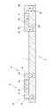
図1は、本実施例のループアンテナ装置の平面図であり、当該装置2は、例えばRFID用のリーダ/ライタに使用される。
また、このアンテナ装置2は、略直方体形状の絶縁基板4の上に螺旋状に巻線された導電体を具備している。DESCRIPTION OF EXEMPLARY EMBODIMENTS Hereinafter, preferred embodiments of the invention will be described with reference to the drawings.
FIG. 1 is a plan view of a loop antenna apparatus according to the present embodiment, and the
The
詳しくは、この基板4は、同図に示されるように、略長方形状の上面6を有し、この上面6の4辺には略長方形状の側面がそれぞれ連なっている。さらに、これら各側面は上面6と同じ面積を有した下面にも連なり、この下面は上面6に対向して配置される。
そして、この上面6には、例えば3回巻き(3ターン)のループを有した導電体が配置されている。Specifically, as shown in the figure, the
A conductor having a loop of, for example, three turns (three turns) is disposed on the
本実施例の装置2は3つのループ10,20,30からなり、これら各ループ10,20,30は、例えば導電性ペーストが基板4にスクリーン印刷されており、螺旋状で一続きに連結している。
より具体的には、まず、ループ10は、これらループ20,30よりも外側に配置され、上面6の周縁に最も近い位置に形成されている。また、このループ10の一端には接続ランド16が形成され、このランド16は図示しない整合回路に接続されている。The
More specifically, first, the
一方、このループ10の他端はループ20に接続される。詳しくは、ループ10は、上面6の4辺に沿って図1でみて時計回りに延び、接続ランド16の近傍位置にてループ20の側面24に接続している。
ここで、本実施例のループ10は、図2に示される如く、断面視で略長方形状に構成された縦置きループ(他方のループ)であり、その側面14の高さがその表面12の幅よりも大きく形成される。On the other hand, the other end of the
Here, as shown in FIG. 2, the
具体的には、当該ループ10は、その側面14の一部分が基板4に埋設し、側面14の残りの部分が上面6から上方に向けて突出しており、幅狭の表面12が上面6に対して略平行に配置される。
次に、ループ20は、ループ10とループ30との間に配置されている。このループ20は、ループ10に対して所定の間隔で配置され、このループ10に沿って図1でみて時計回りに延びており、ループ20の側面24とループ10の側面14とが対峙している。Specifically, a part of the
Next, the
また、このループ20の一端近傍の側面24がループ10の他端に接続され、これらループ20の表面22とループ10の表面12とは略面一で配置される。一方、ループ20の他端は、ループ10とループ20との接続箇所の近傍位置にてループ30に接続される。ループ20の表面22とループ30の表面32ともまた略面一で配置される(図2)。 Further, a
ここで、本実施例のループ20は、断面視で略長方形状に構成された横置きループ(一方のループ)であり、その表面22の幅がその側面24の高さよりも大きく形成されている。当該ループ20の断面積は、ループ10の断面積と略同一の大きさで構成される。
また、当該ループ20は、その表面22に対向した裏面が上面6に載置され、幅広の表面22が上面6に対して略平行に配置されている。Here, the
In addition, the
続いて、ループ30は、ループ10とループ20との間隔に等しい間隔で、ループ20よりも内側に配置されており、このループ20に沿って図1でみて時計回りに延びており、ループ30の側面34とループ20の側面24とが対峙している。
このループ30の一端近傍の側面34はループ20の他端に接続され(図3)、このループ30の他端には接続ランド36が形成される(図1)。このランド36もまた上記整合回路に接続されている。Subsequently, the
A
再び図2に戻り、本実施例のループ30は、上記ループ10と同様に、断面視で略長方形状に構成された縦置きループ(他方のループ)である。つまり、その側面34の高さはその表面32の幅よりも大きく形成されており、さらに、当該ループ30の断面積は、ループ10,20の断面積と略同一の大きさで構成されている。 Returning to FIG. 2 again, the
そして、当該ループ30もまた、その側面34の一部分が基板4に埋設しており、幅狭の表面32が上面6に対して略平行に配置される。
なお、この基板4の上面6の適宜位置には、上述した整合回路の他、図示しないチップ部品や発振器(AC電源)等の電子部品が実装され、これら電子部品もループ10,20,30に接続されている。The
In addition to the matching circuit described above, electronic components such as a chip component and an oscillator (AC power supply) (not shown) are mounted at appropriate positions on the
以上のように、本実施例によれば、ループアンテナ装置2は螺旋状で一続きの導電体を具備し、この導電体は、所定の高さ及び幅を有した断面視で略長方形状のループ10,20,30が3ターン連なって構成され、基板4上に配置されている。 As described above, according to the present embodiment, the
そして、これらループ10,20,30は交互巻きで構成されており、縦置きのループ10と横置きのループ20とが隣接し、この横置きのループ20と縦置きのループ30とが隣接している。
これにより、巻線数を増やしつつも、開口面積が大きく、且つ、Q値も高くなる。These
Thereby, while increasing the number of windings, the opening area is large and the Q value is also high.
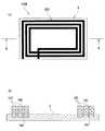
この点について詳述すると、図4に示されたループアンテナ装置100Aの如く、総てのループ200が横置きのループのみで構成された場合には、本実施例の巻線数と同じであったとしても、幅広の表面220が基板4の上面6の多くを占有するので、ループ200の内側に形成された開口面積が小さくなり、アンテナの通信可能距離が短くなってしまう。 This point will be described in detail. When all the
これに対し、図5に示されたループアンテナ装置100Bの如く、総てのループ300が縦置きのループのみで構成された場合には、本実施例の巻線数と同じであるとすれば、幅狭の表面320が基板4の上面6を占めることから、開口面積は大きくなるものの、図4の側面240の大きさと比較しても明らかなように、その側面340が上面6から上方に向けて大きく突出する。 On the other hand, in the case where all the
つまり、これら対峙する側面340,340で形成された空間が非常に大きくなる結果、隣接するループ間の寄生容量が大きくなり、Q値が低くなるので、やはりアンテナの通信可能距離が短くなってしまうのである。
しかしながら、本実施例では交互巻きのループが採用され、縦置きのループ10に続いて横置きのループ20が巻かれ、この横置きのループ20に続いて縦置きのループ30が巻かれている。In other words, the space formed by these opposing side surfaces 340 and 340 becomes very large, and as a result, the parasitic capacitance between adjacent loops increases and the Q value decreases, so the communicable distance of the antenna is also shortened. It is.
However, in this embodiment, an alternating winding loop is adopted, a
したがって、巻線数が増加して線路長が長くなっても、当該縦置きのループ10,30の構成によって開口面積は、上述した図4の装置100Aに比して大きくなり、アンテナの利得が高くなる。よって、このアンテナの通信可能距離が長く、アンテナ効率が高くなる。 Therefore, even if the number of windings is increased and the line length is increased, the configuration of the
しかも、この横置きのループ20の構成によれば、開口面積は上述した図5の装置100Bに比して小さくなるものの、寄生容量が当該装置100Bに比して小さくなり、上述した図4の装置100Aと同じになる。これら対峙する側面14,24(或いは側面24,34)で形成された空間は、ループ10,30の間に配置したループ20の側面24の高さに依存するからである。 Moreover, according to the configuration of the
したがって、当該横置きのループ20の構成によってQ値が高く、損失が小さくなって共振特性が鋭くなり、外部に放出する磁界エネルギが多くなるので、アンテナの通信可能距離が長くなる。
この結果、線路長が長く、開口面積が大きく、且つ、共振特性の鋭いアンテナになり、ループアンテナ装置2の通信品質が良好になる。Therefore, the configuration of the
As a result, the antenna has a long line length, a large opening area, and sharp resonance characteristics, and the communication quality of the
なお、本実施例の構成は、巻線数を図4の装置100Aや図5の装置100Bと同じにした場合について示されているが、開口面積を装置100Aと同じ大きさで考えれば、この装置100Aよりも巻線数を増やせるし、装置100BよりもQ値が依然として高くなるとも云える。 In addition, although the structure of a present Example is shown about the case where the number of windings is made the same as the
また、各ループ10,20,30の断面積をいずれの場所においても略同一にし、狭窄箇所をなくしているので、ループ10,20,30のインピーダンスを低くでき、電力損失が確実に抑えられる。
さらに、横置きのループ20の表面22、及び縦置きのループ10,30の表面12,32が基板4の上面6から最も突出することになるが、これら各表面12,22,32が略面一に配置されているので、このループ20の側面24の高さに抑えられ、ループアンテナ装置2の低背化が達成可能になる。In addition, since the cross-sectional areas of the
Furthermore, the
さらにまた、上記3回巻きの場合には、隣接するループ同士で見ると、両側に縦置きのループ10,30を配置し、その間に横置きのループ20を配置している。
これにより、両側に横置きのループを配置し、その間に縦置きのループを配置した場合に比して開口面積を拡大できるし、また、両側に横置きや縦置きのループを配置し、その間に縦置きのループを配置した場合に比して寄生容量を削減でき、これら開口面積の拡大及び寄生容量の削減の双方を確実に満たすことができる。Furthermore, in the case of the above-described three turns, when viewed from adjacent loops, the vertically placed
This makes it possible to expand the opening area compared to the case where horizontal loops are placed on both sides and a vertical loop is placed between them, and horizontal and vertical loops are placed on both sides. The parasitic capacitance can be reduced as compared with the case where the vertically arranged loop is arranged, and both the expansion of the opening area and the reduction of the parasitic capacitance can be surely satisfied.
本発明は、上記実施例に限定されず、特許請求の範囲を逸脱しない範囲で種々の変更を行うことができる。例えば上記実施例の各構成は、その一部を省略したり、上記とは異なるように任意に組み合わせることができる。
また、本実施例では、横置きのループ20と縦置きのループ10,30との組み合わせで構成されているが、ループが交互巻きで連なっている限り、互いに隣接した一方のループの高さよりも他方のループの高さが大きく、当該一方のループの幅よりも他方のループの幅が小さくされていても良い。The present invention is not limited to the above embodiments, and various modifications can be made without departing from the scope of the claims. For example, a part of the configurations of the above embodiments can be omitted or arbitrarily combined so as to be different from the above.
In the present embodiment, the
換言すれば、本発明のループには、これら一方のループ及び他方のループのいずれもが、その高さよりも幅がそれぞれ大きく形成されている場合も該当する。いずれかのループのみで構成させた場合に比して、開口面積を大きく、寄生容量を小さくできるからである。 In other words, the case where the width of each of the one loop and the other loop is formed larger than the height thereof corresponds to the loop of the present invention. This is because the opening area can be increased and the parasitic capacitance can be reduced as compared with the case where only one of the loops is used.
また、上記実施例では、3回巻きの構成が示されているが必ずしもこの例に限定されるものではなく、さらに、本発明のループアンテナ装置はリーダ/ライタのみならず、ICカードにも適用可能である。
そして、これらいずれの場合にも上記と同様に、巻線数を増やしつつも、開口面積が大きく、且つ、Q値の高いループアンテナ装置になるとの効果を奏する。In the above embodiment, the configuration of three turns is shown, but the configuration is not necessarily limited to this example. Furthermore, the loop antenna device of the present invention is applicable not only to a reader / writer but also to an IC card. Is possible.
In any of these cases, similarly to the above, there is an effect that the loop antenna apparatus having a large opening area and a high Q value is obtained while increasing the number of windings.
2 ループアンテナ装置
4 絶縁基板
6 上面
10 縦置きループ(他方のループ)
12 表面
14 側面
20 横置きループ(一方のループ)
22 表面
24 側面
30 縦置きループ(他方のループ)
32 表面
34 側面2
12
22
32
Claims (5)
Translated fromJapanese該導電体は、所定の高さ及び幅を有した断面視で略長方形状のループが複数連なっており、
該高さ部分が対峙した隣接するループ同士では、一方のループの高さが他方のループの高さよりも小さく、該他方のループの幅が前記一方のループの幅よりも小さいことを特徴とするループアンテナ装置。A loop antenna device comprising a conductor spirally wound on an insulating substrate,
The conductor has a plurality of substantially rectangular loops in a cross-sectional view having a predetermined height and width,
Between adjacent loops facing each other, the height of one loop is smaller than the height of the other loop, and the width of the other loop is smaller than the width of the one loop. Loop antenna device.
前記一方のループの断面積と、前記他方のループの断面積とは略同一の大きさであることを特徴とするループアンテナ装置。The loop antenna device according to claim 1,
The loop antenna device according to claim 1, wherein a cross-sectional area of the one loop and a cross-sectional area of the other loop are substantially the same size.
前記一方のループは、その幅がその高さよりも大きく形成されるのに対し、前記他方のループは、その高さがその幅よりも大きく形成されることを特徴とするループアンテナ装置。The loop antenna device according to claim 1 or 2,
The loop antenna device characterized in that the width of the one loop is formed larger than its height, whereas the height of the other loop is formed larger than its width.
前記他方のループは、その一部分が前記基板に埋設され、該他方のループの幅をなす表面と、前記一方のループの幅をなす表面とが略面一で配置されていることを特徴とするループアンテナ装置。The loop antenna device according to any one of claims 1 to 3,
A part of the other loop is embedded in the substrate, and the surface forming the width of the other loop and the surface forming the width of the one loop are arranged substantially flush with each other. Loop antenna device.
前記導電体が奇数個のターンで連なっている場合には、前記一方のループが前記他方のループの間に配置されることを特徴とするループアンテナ装置。
The loop antenna device according to any one of claims 1 to 4,
When the conductor is connected in an odd number of turns, the one loop is disposed between the other loops.
Priority Applications (4)
| Application Number | Priority Date | Filing Date | Title |
|---|---|---|---|
| JP2008144182AJP2009290829A (en) | 2008-06-02 | 2008-06-02 | Loop antenna device |
| TW098115873ATW201008031A (en) | 2008-06-02 | 2009-05-13 | Loop antenna device with large opening area |
| US12/473,641US20090295658A1 (en) | 2008-06-02 | 2009-05-28 | Loop antenna device with large opening area |
| CNA2009101452931ACN101599574A (en) | 2008-06-02 | 2009-06-01 | The loop antenna apparatus of large opening area |
Applications Claiming Priority (1)
| Application Number | Priority Date | Filing Date | Title |
|---|---|---|---|
| JP2008144182AJP2009290829A (en) | 2008-06-02 | 2008-06-02 | Loop antenna device |
Publications (1)
| Publication Number | Publication Date |
|---|---|
| JP2009290829Atrue JP2009290829A (en) | 2009-12-10 |
Family
ID=41379132
Family Applications (1)
| Application Number | Title | Priority Date | Filing Date |
|---|---|---|---|
| JP2008144182AWithdrawnJP2009290829A (en) | 2008-06-02 | 2008-06-02 | Loop antenna device |
Country Status (4)
| Country | Link |
|---|---|
| US (1) | US20090295658A1 (en) |
| JP (1) | JP2009290829A (en) |
| CN (1) | CN101599574A (en) |
| TW (1) | TW201008031A (en) |
Cited By (3)
| Publication number | Priority date | Publication date | Assignee | Title |
|---|---|---|---|---|
| JP2017192109A (en)* | 2016-04-15 | 2017-10-19 | 株式会社エスケーエレクトロニクス | RFID tag |
| JP2019041273A (en)* | 2017-08-25 | 2019-03-14 | 株式会社村田製作所 | Coil antenna and electronic device |
| JP2020178034A (en)* | 2019-04-18 | 2020-10-29 | 国立大学法人信州大学 | Non-contact power supply transmission coil unit, non-contact power supply transmission coil unit manufacturing method, and non-contact power supply device |
Families Citing this family (5)
| Publication number | Priority date | Publication date | Assignee | Title |
|---|---|---|---|---|
| US10033101B2 (en) | 2015-06-12 | 2018-07-24 | Samsung Electronics Co., Ltd. | Near field communication antenna, near field communication device and mobile system having the same |
| KR101926594B1 (en)* | 2015-08-20 | 2018-12-10 | 주식회사 아모텍 | Antenna unit for a wireless charging and wireless charging module having the same |
| US10692643B2 (en) | 2015-10-27 | 2020-06-23 | Cochlear Limited | Inductance coil path |
| EP3369183A4 (en)* | 2015-10-27 | 2019-06-05 | Cochlear Limited | Inductance coil with varied geometry |
| JP6583901B2 (en)* | 2016-02-11 | 2019-10-02 | ミ ジョン キム, | Monopole antenna |
Citations (2)
| Publication number | Priority date | Publication date | Assignee | Title |
|---|---|---|---|---|
| JP2004287967A (en)* | 2003-03-24 | 2004-10-14 | Toppan Forms Co Ltd | Resonant tag and contactless data receiver |
| JP2009253580A (en)* | 2008-04-04 | 2009-10-29 | Panasonic Corp | Adjustment method of antenna device, and method for manufacturing thereof |
Family Cites Families (4)
| Publication number | Priority date | Publication date | Assignee | Title |
|---|---|---|---|---|
| US6161761A (en)* | 1998-07-09 | 2000-12-19 | Motorola, Inc. | Card assembly having a loop antenna formed of a bare conductor and method for manufacturing the card assembly |
| US6927741B2 (en)* | 2001-11-15 | 2005-08-09 | Merlin Technology, Inc. | Locating technique and apparatus using an approximated dipole signal |
| US20070021667A1 (en)* | 2005-05-19 | 2007-01-25 | Biophan Technologies, Inc. | Electromagnetic resonant circuit sleeve for implantable medical device |
| US7998139B2 (en)* | 2007-04-25 | 2011-08-16 | Vivant Medical, Inc. | Cooled helical antenna for microwave ablation |
- 2008
- 2008-06-02JPJP2008144182Apatent/JP2009290829A/ennot_activeWithdrawn
- 2009
- 2009-05-13TWTW098115873Apatent/TW201008031A/enunknown
- 2009-05-28USUS12/473,641patent/US20090295658A1/ennot_activeAbandoned
- 2009-06-01CNCNA2009101452931Apatent/CN101599574A/enactivePending
Patent Citations (2)
| Publication number | Priority date | Publication date | Assignee | Title |
|---|---|---|---|---|
| JP2004287967A (en)* | 2003-03-24 | 2004-10-14 | Toppan Forms Co Ltd | Resonant tag and contactless data receiver |
| JP2009253580A (en)* | 2008-04-04 | 2009-10-29 | Panasonic Corp | Adjustment method of antenna device, and method for manufacturing thereof |
Cited By (3)
| Publication number | Priority date | Publication date | Assignee | Title |
|---|---|---|---|---|
| JP2017192109A (en)* | 2016-04-15 | 2017-10-19 | 株式会社エスケーエレクトロニクス | RFID tag |
| JP2019041273A (en)* | 2017-08-25 | 2019-03-14 | 株式会社村田製作所 | Coil antenna and electronic device |
| JP2020178034A (en)* | 2019-04-18 | 2020-10-29 | 国立大学法人信州大学 | Non-contact power supply transmission coil unit, non-contact power supply transmission coil unit manufacturing method, and non-contact power supply device |
Also Published As
| Publication number | Publication date |
|---|---|
| CN101599574A (en) | 2009-12-09 |
| US20090295658A1 (en) | 2009-12-03 |
| TW201008031A (en) | 2010-02-16 |
Similar Documents
| Publication | Publication Date | Title |
|---|---|---|
| JP2009290829A (en) | Loop antenna device | |
| JP5673906B1 (en) | Communication terminal | |
| TW516049B (en) | Spiral inductor | |
| JP4894960B2 (en) | Electronics | |
| US20100213265A1 (en) | Contactless device with miniaturized antenna | |
| JP2010200309A (en) | Proximity antenna and wireless communication device | |
| JP2010245776A (en) | Antenna | |
| JP5741782B1 (en) | ANTENNA DEVICE, CARD-TYPE DEVICE, AND ELECTRONIC DEVICE | |
| CN202395152U (en) | Antenna, electronic tag and electronic tag reader | |
| US10074904B2 (en) | Antenna device and coil component used therein | |
| JP6213688B2 (en) | ANTENNA DEVICE AND ELECTRONIC DEVICE | |
| JP5593834B2 (en) | Proximity antenna and wireless communication device | |
| JP4883208B2 (en) | ANTENNA DEVICE AND COMMUNICATION DEVICE HAVING THE SAME | |
| CN103348533B (en) | Antenna device | |
| JP6172407B2 (en) | ANTENNA DEVICE, CARD TYPE INFORMATION MEDIUM, AND COMMUNICATION TERMINAL DEVICE | |
| JP6172418B2 (en) | ANTENNA DEVICE, CARD TYPE INFORMATION MEDIUM, ELECTRONIC DEVICE, AND ANTENNA DEVICE MANUFACTURING METHOD | |
| JP2013009071A (en) | Antenna coil | |
| JP6183688B2 (en) | ANTENNA DEVICE AND WIRELESS COMMUNICATION DEVICE | |
| JP4807464B1 (en) | Antenna device | |
| WO2015129766A1 (en) | Antenna device and portable terminal device | |
| CN109565113B (en) | Antenna device and IC tag using the same | |
| JP2008186327A (en) | Rfid reader | |
| CN105552545A (en) | Near field communication (NFC) antenna device and electronic device | |
| US20170054475A1 (en) | Coil antenna device, electronic apparatus with coil antenna device, and method of producing coil antenna device | |
| JP2011049935A (en) | Antenna device |
Legal Events
| Date | Code | Title | Description |
|---|---|---|---|
| A977 | Report on retrieval | Free format text:JAPANESE INTERMEDIATE CODE: A971007 Effective date:20100405 | |
| A131 | Notification of reasons for refusal | Free format text:JAPANESE INTERMEDIATE CODE: A131 Effective date:20100601 | |
| A521 | Request for written amendment filed | Free format text:JAPANESE INTERMEDIATE CODE: A523 Effective date:20100721 | |
| A761 | Written withdrawal of application | Free format text:JAPANESE INTERMEDIATE CODE: A761 Effective date:20110422 |