JP2009290052A - Method of dividing wafer - Google Patents
Method of dividing waferDownload PDFInfo
- Publication number
- JP2009290052A JP2009290052AJP2008142175AJP2008142175AJP2009290052AJP 2009290052 AJP2009290052 AJP 2009290052AJP 2008142175 AJP2008142175 AJP 2008142175AJP 2008142175 AJP2008142175 AJP 2008142175AJP 2009290052 AJP2009290052 AJP 2009290052A
- Authority
- JP
- Japan
- Prior art keywords
- wafer
- street
- film
- along
- substrate
- Prior art date
- Legal status (The legal status is an assumption and is not a legal conclusion. Google has not performed a legal analysis and makes no representation as to the accuracy of the status listed.)
- Pending
Links
Images


Classifications
- H—ELECTRICITY
- H01—ELECTRIC ELEMENTS
- H01L—SEMICONDUCTOR DEVICES NOT COVERED BY CLASS H10
- H01L21/00—Processes or apparatus adapted for the manufacture or treatment of semiconductor or solid state devices or of parts thereof
- H01L21/70—Manufacture or treatment of devices consisting of a plurality of solid state components formed in or on a common substrate or of parts thereof; Manufacture of integrated circuit devices or of parts thereof
- H01L21/77—Manufacture or treatment of devices consisting of a plurality of solid state components or integrated circuits formed in, or on, a common substrate
- H01L21/78—Manufacture or treatment of devices consisting of a plurality of solid state components or integrated circuits formed in, or on, a common substrate with subsequent division of the substrate into plural individual devices
Landscapes
- Engineering & Computer Science (AREA)
- Physics & Mathematics (AREA)
- Condensed Matter Physics & Semiconductors (AREA)
- General Physics & Mathematics (AREA)
- Manufacturing & Machinery (AREA)
- Computer Hardware Design (AREA)
- Microelectronics & Electronic Packaging (AREA)
- Power Engineering (AREA)
- Laser Beam Processing (AREA)
- Dicing (AREA)
Abstract
Translated fromJapaneseDescription
Translated fromJapanese本発明は、表面に複数のストリートが格子状に形成されているとともに該複数のストリートによって区画された複数の領域にデバイスが形成されたウエーハを、ストリートに沿って分割するウエーハの分割方法に関する。 The present invention relates to a wafer dividing method for dividing a wafer in which a plurality of streets are formed on the surface in a lattice shape and a device is formed in a plurality of regions partitioned by the plurality of streets along the streets.
半導体デバイス製造工程においては、略円板形状である半導体ウエーハの表面に格子状に配列されたストリートと呼ばれる分割予定ラインによって複数の領域が区画され、この区画された領域にIC、LSI、液晶ドライバー、フラッシュメモリ等のデバイスを形成する。そして、ウエーハをストリートに沿って切断することによりデバイスが形成された領域を分割して個々のデバイスを製造している。 In the semiconductor device manufacturing process, a plurality of regions are partitioned by dividing lines called streets arranged in a lattice pattern on the surface of a substantially wafer-shaped semiconductor wafer, and ICs, LSIs, and liquid crystal drivers are divided into these partitioned regions. Form devices such as flash memory. Then, by cutting the wafer along the streets, the regions where the devices are formed are divided to manufacture individual devices.
上述したウエーハのストリートに沿って分割する方法として、ウエーハに対して透過性を有する波長のパルスレーザー光線を用い、分割すべき領域の内部に集光点を合わせてパルスレーザー光線を照射するレーザー加工方法も試みられている。このレーザー加工方法を用いた分割方法は、ウエーハの一方の面側から内部に集光点を合わせてウエーハに対して透過性を有する波長のパルスレーザー光線を照射し、ウエーハの内部にストリートに沿って変質層を連続的に形成し、この変質層が形成されることによって強度が低下したストリートに沿って外力を加えることにより、ウエーハを破断して分割するものであり、ストリートの幅を狭くすることが可能となる。(例えば、特許文献1参照。)
而して、ストリートの表面に金属膜、フッ化シリケートグラス膜、シリコン酸化膜系パシベーション膜(SiO2,SiON)、ポリイミド(PI)系高分子化合物膜、フッ素系高分子化合物膜、フッ素化アモルファスカーボン系化合物膜が被覆されているウエーハにおいては、内部に集光点を合わせてウエーハ基板に対して透過性を有する波長のパルスレーザー光線を照射し、ウエーハの内部にストリートに沿って変質層を形成することにより、ウエーハ基板を分割することはできるが、ストリートの表面に被覆された膜は分割できないという問題がある。 Thus, on the street surface, metal film, fluorinated silicate glass film, silicon oxide film passivation film (SiO2, SiON), polyimide (PI) polymer film, fluorine polymer film, fluorinated amorphous carbon In a wafer coated with a system compound film, a denatured layer is formed along the street inside the wafer by irradiating a pulse laser beam having a wavelength that is transparent to the wafer substrate with the condensing point inside. Thus, the wafer substrate can be divided, but there is a problem that the film coated on the street surface cannot be divided.
本発明は上記事実に鑑みてなされたものであり、その主たる技術的課題は、ストリートの表面に膜が被覆されたウエーハを、膜を残すことなく分割することができるウエーハの分割方法を提供することである。 The present invention has been made in view of the above-mentioned facts, and its main technical problem is to provide a wafer dividing method capable of dividing a wafer having a film coated on the street surface without leaving a film. That is.
上記主たる技術課題を解決するため、本発明によれば、基板の表面に格子状に形成された複数のストリートによって区画された複数の領域にデバイスが形成されているとともに該ストリートの表面に膜が被覆されているウエーハを、該ストリートに沿って個々のデバイスに分割するウエーハの分割方法であって、
ウエーハを構成する該基板の裏面を研削し、ウエーハを所定の厚さに形成する裏面研削工程と、
該基板に対して透過性を有する波長のレーザー光線をウエーハの裏面側から該基板の内部に集光点を位置付けて該ストリートに沿って照射し、該基板の内部にストリートに沿って変質層を形成する変質層形成工程と、
該変質層形成工程が実施されたウエーハの裏面を環状のフレームに装着されたダイシングテープの表面に貼着するウエーハ支持工程と、
該膜に対して吸収性を有する波長のレーザー光線をウエーハの表面側から該ストリートに沿って該膜に照射してレーザー加工溝を形成し、該膜を該ストリートに沿って分断する膜分断工程と、
環状のフレームに装着されたダイシングテープの表面にウエーハの裏面を貼着した状態で該ダイシングテープを拡張することによりウエーハに外力を付与し、ウエーハを該ストリートに沿って破断するウエーハ破断工程と、を含む、
ことを特徴とするウエーハの分割方法が提供される。In order to solve the above main technical problem, according to the present invention, a device is formed in a plurality of regions partitioned by a plurality of streets formed in a lattice shape on the surface of the substrate, and a film is formed on the surface of the streets. A wafer dividing method for dividing a coated wafer into individual devices along the street,
Grinding the back surface of the substrate constituting the wafer and forming a wafer to a predetermined thickness;
A laser beam having a wavelength transmissive to the substrate is irradiated from the back side of the wafer to the inside of the substrate along the street, and a deteriorated layer is formed along the street. An altered layer forming step,
A wafer support step of attaching the rear surface of the wafer subjected to the altered layer forming step to the surface of a dicing tape attached to an annular frame;
A film cutting step of irradiating the film along the street with a laser beam having a wavelength having an absorptivity with respect to the film to form a laser processing groove, and cutting the film along the street; ,
A wafer breaking step of applying an external force to the wafer by expanding the dicing tape in a state where the back surface of the wafer is attached to the surface of the dicing tape attached to the annular frame, and breaking the wafer along the street; including,
A method of dividing a wafer is provided.
また、本発明によれば、基板の表面に格子状に形成された複数のストリートによって区画された複数の領域にデバイスが形成されているとともに該ストリートの表面に膜が被覆されているウエーハを、該ストリートに沿って個々のデバイスに分割するウエーハの分割方法であって、
該基板に対して透過性を有する波長のレーザー光線をウエーハの裏面側から該基板の内部に集光点を位置付けて該ストリートに沿って照射し、該基板の内部にストリートに沿って変質層を形成する変質層形成工程と、
該変質層形成工程が実施されたウエーハを構成する該基板の裏面を研削し、ウエーハを所定の厚さに形成する裏面研削工程と、
該裏面研削工程が実施されたウエーハの裏面を環状のフレームに装着されたダイシングテープの表面に貼着するウエーハ支持工程と、
該膜に対して吸収性を有する波長のレーザー光線をウエーハの表面側から該ストリートに沿って該膜に照射してレーザー加工溝を形成し、該膜を該ストリートに沿って分断する膜分断工程と、
環状のフレームに装着されたダイシングテープの表面にウエーハの裏面を貼着した状態で該ダイシングテープを拡張することによりウエーハに外力を付与し、ウエーハを該ストリートに沿って破断するウエーハ破断工程と、を含む、
ことを特徴とするウエーハの分割方法が提供される。In addition, according to the present invention, a wafer in which a device is formed in a plurality of regions partitioned by a plurality of streets formed in a lattice shape on the surface of the substrate and a film is coated on the surface of the streets, A method for dividing a wafer into individual devices along the street,
A laser beam having a wavelength transmissive to the substrate is irradiated from the back side of the wafer to the inside of the substrate along the street, and a deteriorated layer is formed along the street. An altered layer forming step,
Grinding the back surface of the substrate constituting the wafer subjected to the altered layer forming step, and forming the wafer to a predetermined thickness;
A wafer support step of attaching the back surface of the wafer subjected to the back grinding step to the surface of a dicing tape attached to an annular frame;
A film cutting step of irradiating the film along the street with a laser beam having a wavelength having an absorptivity with respect to the film to form a laser processing groove, and cutting the film along the street; ,
A wafer breaking step of applying an external force to the wafer by expanding the dicing tape in a state where the back surface of the wafer is attached to the surface of the dicing tape attached to the annular frame, and breaking the wafer along the street; including,
A method of dividing a wafer is provided.
本発明におけるウエーハの分割方法によれば、基板の内部にストリートに沿って変質層を形成する変質層形成工程とウエーハの基板に形成されたストリートの表面に被覆された膜をストリートに沿って分断する膜分断工程を実施し後に、ウエーハに外力を付与してウエーハをストリートに沿って破断するので、ウエーハをストリートに沿って破断する際には膜はストリートに沿って分断されているため、膜が破断されずに残ることはない。 According to the wafer dividing method of the present invention, the altered layer forming step of forming an altered layer along the street inside the substrate and the film coated on the surface of the street formed on the wafer substrate are divided along the street. After the film dividing step is performed, an external force is applied to the wafer and the wafer is broken along the street. Therefore, when the wafer is broken along the street, the film is divided along the street. Does not remain unbroken.
以下、本発明によるウエーハの分割方法の好適な実施形態について、添付図面を参照して詳細に説明する。 Preferred embodiments of a wafer dividing method according to the present invention will be described below in detail with reference to the accompanying drawings.
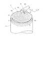
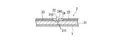
図1には本発明によるウエーハの分割方法によって分割されるウエーハの斜視図が示されており、図2には図1に示すウエーハの要部を拡大した断面図が示されている。図1および図2に示すウエーハ2は、例えば厚さが600μmのシリコン基板21の表面21aに格子状に形成された複数のストリート22によって複数の領域が区画され、この区画された領域にIC、LSI、液晶ドライバー、フラッシュメモリ等のデバイス23が形成されている。このウエーハ2には、図2に示すようにストリート22およびデバイス23を含む表面21aに図示の実施形態においてはポリイミド(PI)系高分子化合物膜24が被覆されている。 FIG. 1 is a perspective view of a wafer divided by the wafer dividing method according to the present invention, and FIG. 2 is an enlarged cross-sectional view of the main part of the wafer shown in FIG. The
上述したウエーハ2を個々のデバイス23に分割するウエーハの分割方法の第1の実施形態について説明する。
第1の実施形態においては、先ずウエーハ2を構成する基板21の裏面21bを研削し、ウエーハ2を所定の厚さに形成する裏面研削工程を実施する。この裏面研削工程を実施するに際し、図示の実施形態においてはウエーハ2の表面に形成されたデバイス23を保護するために、図3の(a)および(b)に示すようにウエーハ2の表面21aに塩化ビニール等からなる保護テープ3を貼着する(保護テープ貼着工程)。A first embodiment of the wafer dividing method for dividing the
In the first embodiment, first, a back surface grinding process is performed in which the
裏面研削工程は、図4の(a)に示す研削装置4を用いて実施する。図4の(a)に示す研削装置4は、被加工物を保持するチャックテーブル41と、該チャックテーブル41に保持された被加工物を研削するための研削砥石42を備えた研削手段43を具備している。この研削装置4を用いて上記裏面研削工程を実施するには、チャックテーブル41上にウエーハ2の保護テープ3側を載置し、図示しない吸引手段を作動することによりウエーハ2をチャックテーブル41上に保持する。従って、チャックテーブル41に保持されたウエーハ2は、裏面21bが上側となる。このようにして、チャックテーブル41上にウエーハ2を保持したならば、チャックテーブル41を矢印41aで示す方向に例えば300rpmで回転しつつ、研削手段43の研削砥石42を矢印42aで示す方向に例えば6000rpmで回転しつつ半導体ウエーハ2の裏面2bに接触せしめて研削することにより、図4の(b)に示すように所定の厚さ(例えば100μm)に形成する。 The back grinding process is performed using a
次に、上述した裏面研削工程が実施されたウエーハ2の基板21に対して透過性を有する波長のレーザー光線をウエーハ2の裏面側から基板21の内部に集光点を位置付けてストリート22に沿って照射し、基板21の内部にストリート22に沿って変質層を形成する変質層形成工程を実施する。この変質層形成工程は、図5に示すレーザー加工装置5を用いて実施する。図5に示すレーザー加工装置5は、被加工物を保持するチャックテーブル51と、該チャックテーブル51上に保持された被加工物にレーザー光線を照射するレーザー光線照射手段52と、チャックテーブル51上に保持された被加工物を撮像する撮像手段53を具備している。チャックテーブル51は、被加工物を吸引保持するように構成されており、図示しない加工送り機構によって図5において矢印Xで示す加工送り方向に移動せしめられるとともに、図示しない割り出し送り機構によって図5において矢印Yで示す割り出し送り方向に移動せしめられるようになっている。 Next, a laser beam having a wavelength that is transmissive to the
上記レーザー光線照射手段52は、実質上水平に配置された円筒形状のケーシング521を含んでいる。ケーシング521内には図示しないYAGレーザー発振器或いはYVO4レーザー発振器からなるパルスレーザー光線発振器や繰り返し周波数設定手段を備えたパルスレーザー光線発振手段が配設されている。このパルスレーザー光線発振手段は、図示の実施形態においては、ウエーハ2の基板21に対して透過性を有する波長(例えば、1064nm)のパルスレーザー光線を発振する。上記ケーシング521の先端部には、パルスレーザー光線発振手段から発振されたパルスレーザー光線を集光するための集光器522が装着されている。 The laser beam irradiation means 52 includes a
上記レーザー光線照射手段52を構成するケーシング521の先端部に装着された撮像手段53は、可視光線によって撮像する通常の撮像素子(CCD)の外に、被加工物に赤外線を照射する赤外線照明手段と、該赤外線照明手段によって照射された赤外線を捕らえる光学系と、該光学系によって捕らえられた赤外線に対応した電気信号を出力する撮像素子(赤外線CCD)等で構成されている。この撮像手段53は、撮像した画像信号を図示しない制御手段に送る。 The imaging means 53 attached to the tip of the
図5に示すレーザー加工装置5を用いて変質層形成工程を実施するには、図5に示すようにチャックテーブル51上にウエーハ2の表面21aに貼着された保護テープ3側を載置する。そして、図示しない吸引手段を作動することにより、保護テープ3を介してウエーハ2をチャックテーブル51上に保持する(ウエーハ保持工程)。従って、チャックテーブル51に保持されたウエーハ2は、裏面21bが上側となる。このようにして、ウエーハ2を吸引保持したチャックテーブル51は、図示しない加工送り機構によって撮像手段53の直下に位置付けられる。 In order to carry out the deteriorated layer forming step using the
チャックテーブル51が撮像手段53の直下に位置付けられると、撮像手段53および図示しない制御手段によってウエーハ2のレーザー加工すべき加工領域を検出するアライメント工程を実行する。即ち、撮像手段53および図示しない制御手段は、ウエーハ2に形成されているストリート22と、ストリート22に沿ってレーザー光線を照射するレーザー光線照射手段52の集光器522との位置合わせを行うためのパターンマッチング等の画像処理を実行し、レーザー光線照射位置のアライメントを遂行する。このアライメント工程を実施する際にはウエーハ2のストリート22が形成されている表面21aは下側に位置しているが、撮像手段53が上述したように赤外線照明手段と赤外線を捕らえる光学系および赤外線に対応した電気信号を出力する撮像素子(赤外線CCD)等で構成された撮像手段を備えているので、裏面21bから透かしてストリート22を撮像することができる。 When the chuck table 51 is positioned immediately below the image pickup means 53, an alignment process for detecting a processing region to be laser processed on the
以上のようにしてチャックテーブル51上に保持されたウエーハ2のレーザー加工すべき加工領域を検出するアライメントが行われたならば、図6の(a)で示すようにチャックテーブル51をレーザー光線を照射するレーザー光線照射手段52の集光器522が位置するレーザー光線照射領域に移動し、所定のストリート22の一端(図6の(a)において左端)をレーザー光線照射手段52の集光器522の直下に位置付ける。そして、集光器522からシリコン基板21に対して透過性を有する波長のパルスレーザー光線を照射しつつチャックテーブル51を図6の(a)において矢印X1で示す方向に所定の加工送り速度で移動せしめる。そして、図6の(b)で示すようにレーザー光線照射手段52の集光器522の照射位置がストリート22の他端(図6の(b)において右端)の位置に達したら、パルスレーザー光線の照射を停止するとともにチャックテーブル51の移動を停止する。この変質層形成工程においては、パルスレーザー光線の集光点Pを半導体ウエーハ2の厚さ方向中間部に位置付ける。この結果、ウエーハ2の基板21には、図6の(b)および図7に示すようにストリート22に沿って厚さ方向中間部に変質層210が形成される。このようにウエーハ2の基板21の内部にストリート22に沿って変質層210が形成されると、基板21には図7に示すように変質層210から表面21aおよび裏面21bに向けてストリート22に沿ってクラック211が発生する。 When the alignment for detecting the processing area to be laser-processed of the
上記変質層形成工程における加工条件は、例えば次のように設定されている。
光源 :LD励起QスイッチNd:YVO4レーザー
波長 :1064nmのパルスレーザー
平均出力 :1W
パルス幅 :40ns
繰り返し周波数 :100kHz
集光スポット径 :φ1μm
加工送り速度 :100mm/秒The processing conditions in the deteriorated layer forming step are set as follows, for example.
Light source: LD excitation Q switch Nd: YVO4 laser Wavelength: 1064 nm pulse laser Average output: 1 W
Pulse width: 40 ns
Repetition frequency: 100 kHz
Condensing spot diameter: φ1μm
Processing feed rate: 100 mm / sec
以上のようにして、ウエーハ2の所定方向に延在する全てのストリート22に沿って上述した変質層形成工程を実行したならば、チャックテーブル51を90度回動せしめて、上記所定方向に対して直角に延びる各ストリート22に沿って上述した変質層形成工程を実行する。 As described above, when the above-described deteriorated layer forming step is performed along all the
次に、上述した変質層形成工程が実施されたウエーハ2の裏面を環状のフレームに装着されたダイシングテープの表面に貼着するウエーハ支持工程を実施する。即ち、図8に示すように環状のフレームFに装着されたダイシングテープTの表面にウエーハ2における基板21の裏面21bを貼着する(ウエーハ支持工程)。そして、ウエーハ2における基板21の表面21aに貼着されている保護テープ3を剥離する(保護テープ剥離工程)。 Next, a wafer support process is performed in which the back surface of the
以上のようにしてウエーハ支持工程および保護テープ剥離工程を実施したならば、上記ウエーハ2を構成する基板21の表面21aに被覆された高分子化合物膜24に対して吸収性を有する波長のレーザー光線をウエーハの表面側からストリート22に沿って高分子化合物膜24に照射してレーザー加工溝を形成し、高分子化合物膜24をストリートに沿って分断する膜分断工程を実施する。この膜分断工程は、図9に示すように上記図5に示すレーザー加工装置5と同様のレーザー加工装置5を用いて実施する。従って、レーザー加工装置5の各構成部材には図5に示す符号と同一符号を付して説明する。なお、レーザー光線照射手段52は、高分子化合物膜24に対して吸収性を有する波長(例えば、355nm)のパルスレーザー光線を発振するパルスレーザー光線発振手段を備えている。 When the wafer support step and the protective tape peeling step are performed as described above, a laser beam having a wavelength that absorbs the
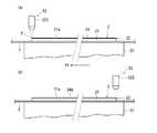
上述したレーザー加工装置5を用いて実施する膜分断工程について、図9乃至図11を参照して説明する。
膜分断工程は、先ず上述した図9に示すレーザー加工装置5のチャックテーブル51上にウエーハ2の裏面21bが貼着されたダイシングテープT側を載置する。そして、図示しない吸引手段を作動することにより、ウエーハ2をチャックテーブル51上に保持する(ウエーハ保持工程)。従って、チャックテーブル51に保持されたウエーハ2は、表面21aが上側となる。なお、図9においてはダイシングテープTが装着された環状のフレームFを省いて示しているが、環状のフレームFはチャックテーブル51に配設された適宜のフレーム保持手段に保持される。The film cutting process performed using the
In the film dividing step, first, the dicing tape T side on which the
上述したようにウエーハ2を吸引保持したチャックテーブル51は、図示しない加工送り機構によって撮像手段53の直下に位置付けられる。チャックテーブル51が撮像手段53の直下に位置付けられると、撮像手段53および図示しない制御手段によってウエーハ2のレーザー加工すべき加工領域を検出するアライメント作業を実行する。即ち、撮像手段53および図示しない制御手段は、ウエーハ2の所定方向に形成されているストリート22と、ストリート22に沿ってレーザー光線を照射するレーザー光線照射手段52の集光器522との位置合わせを行うためのパターンマッチング等の画像処理を実行し、レーザー光線照射位置のアライメントを遂行する。また、ウエーハ2に形成されている上記所定方向に対して直角に延びるストリート22に対しても、同様にレーザー光線照射位置のアライメントが遂行される(アライメント工程)。なお、アライメント工程においては、ウエーハ2のストリート22およびデバイス23を含む表面21aに被覆されたポリイミド(PI)系高分子化合物膜24が透明でない場合でも、撮像手段53が上述したように赤外線照明手段と赤外線を捕らえる光学系および赤外線に対応した電気信号を出力する撮像素子(赤外線CCD)等で構成された撮像手段を備えているので、ポリイミド(PI)系高分子化合物膜24を透過してストリート22を撮像することができる。 As described above, the chuck table 51 that sucks and holds the
以上のようにしてチャックテーブル51上に保持されたウエーハ2に形成されているストリート22を検出し、レーザー光線照射位置のアライメントが行われたならば、図10の(a)で示すようにチャックテーブル51をレーザー光線を照射するレーザー光線照射手段52の集光器522が位置するレーザー光線照射領域に移動し、所定のストリート22を集光器522の直下に位置付ける。このとき、図10の(a)で示すように半導体ウエーハ2は、ストリート22の一端(図10の(a)において左端)が集光器522の直下に位置するように位置付けられる。次に、レーザー光線照射手段52の集光器522からウエーハ2の高分子化合物膜24に対して吸収性を有する波長のパルスレーザー光線を照射しつつチャックテーブル51を図10の(a)において矢印X1で示す方向に所定の加工送り速度で移動せしめる。そして、図10の(b)で示すようにストリート22の他端(図10の(b)において右端)が集光器522の直下位置に達したら、パルスレーザー光線の照射を停止するとともにチャックテーブル51の移動を停止する。この膜分断工程においては、パルスレーザー光線の集光点Pをウエーハ2の表面に被覆された高分子化合物膜24の表面(上面)付近に合わせる。 When the
上述した膜分断工程を実施することにより、図11に示すように高分子化合物膜24にはストリート22に沿って基板21に達するレーザー加工溝240が形成される。この結果、ストリート22に被覆された高分子化合物膜24は、レーザー加工溝240によってストリート22に沿って分断される。この膜分断工程においては、高分子化合物膜24はレーザー加工するが直ちに昇華され、シリコンからなる基板21は加工しないので、レーザー加工によるデブリの発生が抑制される。 By performing the above-described film dividing step, a
なお、上記膜分断工程は、例えば以下の加工条件で行われる。
レーザー光線の光源 :LD励起QスイッチNd:YVO4レーザー
波長 :355nm
平均出力 :1W
パルス幅 :40ns
繰り返し周波数 :50kHz
集光スポット径 :φ5μm
加工送り速度 :100mm/秒In addition, the said film | membrane parting process is performed on the following process conditions, for example.
Laser light source: LD pumped Q-switched Nd: YVO4 laser Wavelength: 355 nm
Average output: 1W
Pulse width: 40 ns
Repetition frequency: 50 kHz
Condensing spot diameter: φ5μm
Processing feed rate: 100 mm / sec
以上のようにして、ウエーハ2の所定方向に延在する全てのストリート22に沿って上述した膜分断工程を実行したならば、チャックテーブル51を90度回動せしめて、上記所定方向に対して直角に延びる各ストリート22に沿って上述した保護膜分断工程を実行する。 As described above, when the above-described film dividing step is performed along all the
以上のようにして膜分断工程を実施したならば、上記膜分断工程および変質層形成工程が実施されているウエーハ2、即ち高分子化合物膜24がストリート22に沿って分断されるとともに21基板の内部にストリート22に沿って変質層210が形成されたウエーハ2に外力を付与し、ウエーハ2をストリート22に沿って破断するウエーハ破断工程を実施する。このウエーハ破断工程は、図示の実施形態においては図12に示すテープ拡張装置6を用いて実施する。図12に示すテープ拡張装置6は、上記環状のフレームFを保持するフレーム保持手段61と、該フレーム保持手段61に保持された環状のフレームFに装着されたダイシングテープTを拡張するテープ拡張手段62を具備している。フレーム保持手段61は、環状のフレーム保持部材611と、該フレーム保持部材611の外周に配設された固定手段としての複数のクランプ612とからなっている。フレーム保持部材611の上面には環状のフレームFを載置する載置面611aが形成されており、この載置面611a上に環状のフレームFが載置される。そして、載置面611a上に載置された環状のフレームFは、クランプ612によってフレーム保持部材611に固定される。このように構成されたフレーム保持手段61は、テープ拡張手段62によって上下方向に進退可能に支持されている。 When the film dividing step is performed as described above, the
テープ拡張手段62は、上記環状のフレーム保持部材611の内側に配設される拡張ドラム621を具備している。この拡張ドラム621は、環状のフレームFの内径より小さく該環状のフレームFに装着されたダイシングテープTに貼着されるウエーハ2の外径より大きい内径および外径を有している。また、拡張ドラム621は、下端に支持フランジ622を備えている。図示の実施形態におけるテープ拡張手段62は、上記環状のフレーム保持部材611を上下方向に進退可能な支持手段63を具備している。この支持手段63は、上記支持フランジ622上に配設された複数のエアシリンダ631からなっており、そのピストンロッド632が上記環状のフレーム保持部材611の下面に連結される。このように複数のエアシリンダ631からなる支持手段63は、環状のフレーム保持部材611を載置面611aが拡張ドラム621の上端と略同一高さとなる基準位置と、拡張ドラム621の上端より所定量下方の拡張位置の間を上下方向に移動せしめる。従って、複数のエアシリンダ631からなる支持手段63は、拡張ドラム621とフレーム保持部材611とを上下方向に相対移動する拡張移動手段として機能する。 The tape expansion means 62 includes an
以上のように構成されたテープ拡張装置6を用いて実施するウエーハ破断工程について図13を参照して説明する。即ち、ウエーハ2(ストリート22に沿って基板21にクラック211が形成されているとともに高分子化合物膜24にレーザー加工溝240が形成されている)の裏面21bが貼着されているダイシングテープTが装着された環状のフレームFを、図13の(a)に示すようにフレーム保持手段61を構成するフレーム保持部材611の載置面611a上に載置し、クランプ612によってフレーム保持部材611に固定する。このとき、フレーム保持部材611は図13の(a)に示す基準位置に位置付けられている。次に、テープ拡張手段62を構成する支持手段63としての複数のエアシリンダ631を作動して、環状のフレーム保持部材611を図13の(b)に示す拡張位置に下降せしめる。従って、フレーム保持部材611の載置面611a上に固定されている環状のフレームFも下降するため、図13の(b)に示すように環状のフレームFに装着されたダイシングテープTは拡張ドラム621の上端縁に接して拡張せしめられる。この結果、ダイシングテープTに貼着されているウエーハ2には放射状に引張力が作用するため、ウエーハ2の基板21は変質層210およびクラック211が形成されることによって強度が低下せしめられたストリート22に沿って破断され個々のデバイス23に分割される。このとき、ウエーハ2の基板21の表面に被覆されている高分子化合物膜24はストリート22に沿って形成されたレーザー加工溝240によって分断されているので、破断されずに残ることはない。 A wafer breaking step performed using the tape expansion device 6 configured as described above will be described with reference to FIG. That is, the dicing tape T to which the
次に、本発明によるウエーハの分割方法の第2の実施形態について説明する。
第2の実施形態においては、先ずウエーハ2の基板21に対して透過性を有する波長のレーザー光線をウエーハ2の裏面側から基板21の内部に集光点を位置付けてストリート22に沿って照射し、基板21の内部にストリート22に沿って変質層を形成する変質層形成工程を実施する。この変質層形成工程を実施するに際し、ウエーハ2の表面に形成されたデバイス23を保護するために、上記図3の(a)および(b)に示すようにウエーハ2の表面21aに塩化ビニール等からなる保護テープ3を貼着する(保護テープ貼着工程)。そして、上記図5に示すようにレーザー加工装置5を用いて上記図6に示す変質層形成工程と同様に実施する。この結果、図14に示すようにウエーハ2の基板21には、内部にストリート22に沿って変質層210が形成されるとともに、変質層210から表面21aおよび裏面21bに向けてクラック211が発生する。Next, a second embodiment of the wafer dividing method according to the present invention will be described.
In the second embodiment, first, a laser beam having a wavelength that is transmissive to the
上述した変質層形成工程を実行したならば、ウエーハ2を構成する基板21の裏面21bを研削し、ウエーハ2を所定の厚さに形成する裏面研削工程を実施する。この裏面研削工程は、図4の(a)に示す研削装置4を用いて上記第1の実施形態における裏面研削工程と同様に実施する。この結果、図15に示すようにウエーハ2は、基板21の裏面21bが研削されて所定の厚さ(例えば100μm)に形成される。なお、上記変質層形成工程において形成される変質層210をウエーハ2の表面2aから例えば100μm以内の位置に形成すれば上記裏面研削工程を実施した後にも変質層210は残るが、上記変質層形成工程において形成される変質層210をウエーハ2の表面2aから例えば100μmの位置より裏面2bに形成することにより、上記裏面研削工程を実施することにより変質層210が形成された位置まで研削され、変質層210は除去される。従って、ウエーハ2の基板21には、図15に示すようにストリート22に沿って形成されたクラック211が残される。 If the above-described deteriorated layer forming step is executed, the back surface grinding step of grinding the
次に、上述した裏面研削工程が実施されたウエーハ2の裏面を環状のフレームに装着されたダイシングテープの表面に貼着するウエーハ支持工程を実施する。このウエーハ支持工程は、上記図8に示すウエーハ支持工程と同様に実施し、ウエーハ2における基板21の表面21aに貼着されている保護テープ3を剥離する(保護テープ剥離工程)。 Next, a wafer support process is performed in which the back surface of the
上述したウエーハ支持工程および保護テープ剥離工程を実施したならば、上記ウエーハ2を構成する基板21の表面21aに被覆された高分子化合物膜24に対して吸収性を有する波長のレーザー光線をウエーハの表面側からストリート22に沿って高分子化合物膜24に照射してレーザー加工溝を形成し、高分子化合物膜24をストリートに沿って分断する膜分断工程を実施する。この膜分断工程は、上記図9に示すレーザー加工装置5を用いて、上記図10に示す膜分断工程と同様に実施する。この結果、図16に示すようにストリート22に被覆された高分子化合物膜24は、レーザー加工溝240によってストリート22に沿って分断される。 If the wafer supporting step and the protective tape peeling step described above are performed, a laser beam having a wavelength that absorbs the
上記膜分断工程を実施したならば、ウエーハ2に外力を付与しウエーハ2をストリート22に沿って破断するウエーハ破断工程を実施する。このウエーハ破断工程は、上記図12に示すテープ拡張装置6を用いて上記図13に示すウエーハ破断工程と同様に実施する。この結果、ウエーハ2の基板21はクラック211が形成されることによって強度が低下せしめられたストリート22に沿って破断され個々のデバイス23に分割される。このとき、ウエーハ2の基板21の表面に被覆されている高分子化合物膜24は上述したようにストリート22に沿って形成されたレーザー加工溝240によって分断されているので、破断されずに残ることはない。 When the film dividing step is performed, an external force is applied to the
上述した実施形態においては、上記裏面研削工程でウエーハ2の基板21の裏面を研削して変質層210が除去されており、ウエーハ2は基板21に形成されたクラック211に沿って破断される。従って、個々の分割されたデバイス23の破断面には変質層210が残存しないため、デバイス23の抗折強度が向上する。 In the above-described embodiment, the deteriorated
2:ウエーハ
21:基板
210:変質層
211:クラック
22:ストリート
23:デバイス
24:高分子化合物膜
240:レーザー加工溝
3:保護テープ
4:研削装置
41:研削装置のチャックテーブル
42:研削砥石
43:研削手段
5:レーザー加工装置
51:レーザー加工装置のチャックテーブル
52:レーザー光線照射手段
6:テープ拡張装置
61:フレーム保持手段
62:テープ拡張手段
F:環状のフレーム
T:ダイシングテープ2: Wafer 21: Substrate 210: Altered layer 211: Crack 22: Street 23: Device 24: Polymer compound film 240: Laser processing groove 3: Protective tape 4: Grinding device 41: Chuck table of grinding device 42: Grinding wheel 43 : Grinding means 5: laser processing apparatus 51: chuck table of laser processing apparatus 52: laser beam irradiation means 6: tape expansion device 61: frame holding means 62: tape expansion means
F: Ring frame
T: Dicing tape
Claims (2)
Translated fromJapaneseウエーハを構成する該基板の裏面を研削し、ウエーハを所定の厚さに形成する裏面研削工程と、
該基板に対して透過性を有する波長のレーザー光線をウエーハの裏面側から該基板の内部に集光点を位置付けて該ストリートに沿って照射し、該基板の内部にストリートに沿って変質層を形成する変質層形成工程と、
該変質層形成工程が実施されたウエーハの裏面を環状のフレームに装着されたダイシングテープの表面に貼着するウエーハ支持工程と、
該膜に対して吸収性を有する波長のレーザー光線をウエーハの表面側から該ストリートに沿って該膜に照射してレーザー加工溝を形成し、該膜を該ストリートに沿って分断する膜分断工程と、
環状のフレームに装着されたダイシングテープの表面にウエーハの裏面を貼着した状態で該ダイシングテープを拡張することによりウエーハに外力を付与し、ウエーハを該ストリートに沿って破断するウエーハ破断工程と、を含む、
ことを特徴とするウエーハの分割方法。A wafer in which a device is formed in a plurality of regions partitioned by a plurality of streets formed in a lattice pattern on the surface of the substrate and a film is coated on the surface of the street is provided along each of the devices along the street. A method of dividing a wafer into
Grinding the back surface of the substrate constituting the wafer and forming a wafer to a predetermined thickness;
A laser beam having a wavelength transmissive to the substrate is irradiated from the back side of the wafer to the inside of the substrate along the street, and a deteriorated layer is formed along the street. An altered layer forming step,
A wafer support step of attaching the rear surface of the wafer subjected to the altered layer forming step to the surface of a dicing tape attached to an annular frame;
A film cutting step of irradiating the film along the street with a laser beam having a wavelength having an absorptivity with respect to the film to form a laser processing groove, and cutting the film along the street; ,
A wafer breaking step of applying an external force to the wafer by expanding the dicing tape in a state where the back surface of the wafer is attached to the surface of the dicing tape attached to the annular frame, and breaking the wafer along the street; including,
A wafer dividing method characterized by the above.
該基板に対して透過性を有する波長のレーザー光線をウエーハの裏面側から該基板の内部に集光点を位置付けて該ストリートに沿って照射し、該基板の内部にストリートに沿って変質層を形成する変質層形成工程と、
該変質層形成工程が実施されたウエーハを構成する該基板の裏面を研削し、ウエーハを所定の厚さに形成する裏面研削工程と、
該裏面研削工程が実施されたウエーハの裏面を環状のフレームに装着されたダイシングテープの表面に貼着するウエーハ支持工程と、
該膜に対して吸収性を有する波長のレーザー光線をウエーハの表面側から該ストリートに沿って該膜に照射してレーザー加工溝を形成し、該膜を該ストリートに沿って分断する膜分断工程と、
環状のフレームに装着されたダイシングテープの表面にウエーハの裏面を貼着した状態で該ダイシングテープを拡張することによりウエーハに外力を付与し、ウエーハを該ストリートに沿って破断するウエーハ破断工程と、を含む、
ことを特徴とするウエーハの分割方法。A wafer in which a device is formed in a plurality of regions partitioned by a plurality of streets formed in a lattice pattern on the surface of the substrate and a film is coated on the surface of the street is provided along each of the devices along the street. A method of dividing a wafer into
A laser beam having a wavelength transmissive to the substrate is irradiated from the back side of the wafer to the inside of the substrate along the street, and a deteriorated layer is formed along the street. An altered layer forming step,
Grinding the back surface of the substrate constituting the wafer subjected to the altered layer forming step, and forming the wafer to a predetermined thickness;
A wafer support step of attaching the back surface of the wafer subjected to the back grinding step to the surface of a dicing tape attached to an annular frame;
A film cutting step of irradiating the film along the street with a laser beam having a wavelength having an absorptivity with respect to the film to form a laser processing groove, and cutting the film along the street; ,
A wafer breaking step of applying an external force to the wafer by expanding the dicing tape in a state where the back surface of the wafer is attached to the surface of the dicing tape attached to the annular frame, and breaking the wafer along the street; including,
A wafer dividing method characterized by the above.
Priority Applications (3)
| Application Number | Priority Date | Filing Date | Title |
|---|---|---|---|
| JP2008142175AJP2009290052A (en) | 2008-05-30 | 2008-05-30 | Method of dividing wafer |
| TW098108917ATW200949924A (en) | 2008-05-30 | 2009-03-19 | Wafer dividing method |
| KR1020090034286AKR20090124928A (en) | 2008-05-30 | 2009-04-20 | Wafer Segmentation Method |
Applications Claiming Priority (1)
| Application Number | Priority Date | Filing Date | Title |
|---|---|---|---|
| JP2008142175AJP2009290052A (en) | 2008-05-30 | 2008-05-30 | Method of dividing wafer |
Publications (1)
| Publication Number | Publication Date |
|---|---|
| JP2009290052Atrue JP2009290052A (en) | 2009-12-10 |
Family
ID=41458964
Family Applications (1)
| Application Number | Title | Priority Date | Filing Date |
|---|---|---|---|
| JP2008142175APendingJP2009290052A (en) | 2008-05-30 | 2008-05-30 | Method of dividing wafer |
Country Status (3)
| Country | Link |
|---|---|
| JP (1) | JP2009290052A (en) |
| KR (1) | KR20090124928A (en) |
| TW (1) | TW200949924A (en) |
Cited By (9)
| Publication number | Priority date | Publication date | Assignee | Title |
|---|---|---|---|---|
| JP2013058536A (en)* | 2011-09-07 | 2013-03-28 | Disco Abrasive Syst Ltd | Method for dividing device wafer |
| JP2015005648A (en)* | 2013-06-21 | 2015-01-08 | 株式会社ディスコ | Wafer processing method |
| JP2019012848A (en)* | 2018-10-03 | 2019-01-24 | 株式会社東京精密 | Wafer processing method and wafer processing system |
| JP2019012849A (en)* | 2018-10-03 | 2019-01-24 | 株式会社東京精密 | Wafer processing method and wafer processing system |
| JP2019012850A (en)* | 2018-10-03 | 2019-01-24 | 株式会社東京精密 | Wafer processing method and wafer processing system |
| JP2020074414A (en)* | 2019-12-25 | 2020-05-14 | 株式会社東京精密 | Laser processing equipment for semiconductor wafers to obtain chips with high bending strength |
| JP2021019136A (en)* | 2019-07-22 | 2021-02-15 | 株式会社ディスコ | Processing method of wafer |
| JP2021045784A (en)* | 2019-09-20 | 2021-03-25 | 株式会社東京精密 | Laser processing device and diagnostic method for laser processing device |
| US12087630B2 (en) | 2021-01-27 | 2024-09-10 | Disco Corporation | Chip manufacturing method |
Families Citing this family (3)
| Publication number | Priority date | Publication date | Assignee | Title |
|---|---|---|---|---|
| TWI401738B (en)* | 2009-12-18 | 2013-07-11 | Chipmos Technologies Inc | Method for dicing a mems wafer |
| KR101803790B1 (en) | 2013-04-18 | 2017-12-04 | 한화테크윈 주식회사 | Thinning method and apparatus of wafer |
| JP6951124B2 (en)* | 2017-05-23 | 2021-10-20 | 株式会社ディスコ | Processing method |
Citations (2)
| Publication number | Priority date | Publication date | Assignee | Title |
|---|---|---|---|---|
| JP2005064232A (en)* | 2003-08-12 | 2005-03-10 | Disco Abrasive Syst Ltd | Wafer processing method |
| JP2007173475A (en)* | 2005-12-21 | 2007-07-05 | Disco Abrasive Syst Ltd | Wafer division method |
- 2008
- 2008-05-30JPJP2008142175Apatent/JP2009290052A/enactivePending
- 2009
- 2009-03-19TWTW098108917Apatent/TW200949924A/enunknown
- 2009-04-20KRKR1020090034286Apatent/KR20090124928A/ennot_activeCeased
Patent Citations (2)
| Publication number | Priority date | Publication date | Assignee | Title |
|---|---|---|---|---|
| JP2005064232A (en)* | 2003-08-12 | 2005-03-10 | Disco Abrasive Syst Ltd | Wafer processing method |
| JP2007173475A (en)* | 2005-12-21 | 2007-07-05 | Disco Abrasive Syst Ltd | Wafer division method |
Cited By (10)
| Publication number | Priority date | Publication date | Assignee | Title |
|---|---|---|---|---|
| JP2013058536A (en)* | 2011-09-07 | 2013-03-28 | Disco Abrasive Syst Ltd | Method for dividing device wafer |
| JP2015005648A (en)* | 2013-06-21 | 2015-01-08 | 株式会社ディスコ | Wafer processing method |
| JP2019012848A (en)* | 2018-10-03 | 2019-01-24 | 株式会社東京精密 | Wafer processing method and wafer processing system |
| JP2019012849A (en)* | 2018-10-03 | 2019-01-24 | 株式会社東京精密 | Wafer processing method and wafer processing system |
| JP2019012850A (en)* | 2018-10-03 | 2019-01-24 | 株式会社東京精密 | Wafer processing method and wafer processing system |
| JP2021019136A (en)* | 2019-07-22 | 2021-02-15 | 株式会社ディスコ | Processing method of wafer |
| JP2021045784A (en)* | 2019-09-20 | 2021-03-25 | 株式会社東京精密 | Laser processing device and diagnostic method for laser processing device |
| JP7324985B2 (en) | 2019-09-20 | 2023-08-14 | 株式会社東京精密 | LASER PROCESSING DEVICE AND LASER PROCESSING DEVICE DIAGNOSTIC METHOD |
| JP2020074414A (en)* | 2019-12-25 | 2020-05-14 | 株式会社東京精密 | Laser processing equipment for semiconductor wafers to obtain chips with high bending strength |
| US12087630B2 (en) | 2021-01-27 | 2024-09-10 | Disco Corporation | Chip manufacturing method |
Also Published As
| Publication number | Publication date |
|---|---|
| TW200949924A (en) | 2009-12-01 |
| KR20090124928A (en) | 2009-12-03 |
Similar Documents
| Publication | Publication Date | Title |
|---|---|---|
| JP5495511B2 (en) | Wafer division method | |
| JP2009290148A (en) | Method of dividing wafer | |
| JP2009290052A (en) | Method of dividing wafer | |
| JP2008277414A (en) | Wafer division method | |
| JP5992731B2 (en) | Wafer processing method | |
| JP4847199B2 (en) | Breaking method of adhesive film attached to wafer | |
| JP6062287B2 (en) | Wafer processing method | |
| JP6305853B2 (en) | Wafer processing method | |
| JP4767711B2 (en) | Wafer division method | |
| JP4977432B2 (en) | Laser processing method of gallium arsenide wafer | |
| JP6466692B2 (en) | Wafer processing method | |
| JP2007173475A (en) | Wafer division method | |
| JP5860217B2 (en) | Laser processing equipment | |
| JP2009200140A (en) | Method of manufacturing semiconductor chip | |
| JP2009206162A (en) | Method of dividing wafer | |
| JP2008235650A (en) | Device manufacturing method | |
| JP2009182178A (en) | Device manufacturing method | |
| JP2008294191A (en) | Wafer division method | |
| JP2011003757A (en) | Method of dividing wafer | |
| JP5906265B2 (en) | Wafer division method | |
| JP2006229021A (en) | Wafer division method | |
| JP2006108273A (en) | Wafer dividing method and dividing apparatus | |
| JP5860219B2 (en) | Laser processing equipment | |
| JP2006344795A (en) | Wafer division method | |
| JP2007012878A (en) | Wafer division method |
Legal Events
| Date | Code | Title | Description |
|---|---|---|---|
| A621 | Written request for application examination | Free format text:JAPANESE INTERMEDIATE CODE: A621 Effective date:20110422 | |
| A977 | Report on retrieval | Free format text:JAPANESE INTERMEDIATE CODE: A971007 Effective date:20130117 | |
| A131 | Notification of reasons for refusal | Free format text:JAPANESE INTERMEDIATE CODE: A131 Effective date:20130212 | |
| A02 | Decision of refusal | Free format text:JAPANESE INTERMEDIATE CODE: A02 Effective date:20130702 |