JP2009288734A - Image display device - Google Patents
Image display deviceDownload PDFInfo
- Publication number
- JP2009288734A JP2009288734AJP2008144061AJP2008144061AJP2009288734AJP 2009288734 AJP2009288734 AJP 2009288734AJP 2008144061 AJP2008144061 AJP 2008144061AJP 2008144061 AJP2008144061 AJP 2008144061AJP 2009288734 AJP2009288734 AJP 2009288734A
- Authority
- JP
- Japan
- Prior art keywords
- voltage
- transistor
- drive transistor
- pixel circuit
- light emitting
- Prior art date
- Legal status (The legal status is an assumption and is not a legal conclusion. Google has not performed a legal analysis and makes no representation as to the accuracy of the status listed.)
- Pending
Links
Images


Classifications
- G—PHYSICS
- G09—EDUCATION; CRYPTOGRAPHY; DISPLAY; ADVERTISING; SEALS
- G09G—ARRANGEMENTS OR CIRCUITS FOR CONTROL OF INDICATING DEVICES USING STATIC MEANS TO PRESENT VARIABLE INFORMATION
- G09G3/00—Control arrangements or circuits, of interest only in connection with visual indicators other than cathode-ray tubes
- G09G3/20—Control arrangements or circuits, of interest only in connection with visual indicators other than cathode-ray tubes for presentation of an assembly of a number of characters, e.g. a page, by composing the assembly by combination of individual elements arranged in a matrix no fixed position being assigned to or needed to be assigned to the individual characters or partial characters
- G09G3/22—Control arrangements or circuits, of interest only in connection with visual indicators other than cathode-ray tubes for presentation of an assembly of a number of characters, e.g. a page, by composing the assembly by combination of individual elements arranged in a matrix no fixed position being assigned to or needed to be assigned to the individual characters or partial characters using controlled light sources
- G09G3/30—Control arrangements or circuits, of interest only in connection with visual indicators other than cathode-ray tubes for presentation of an assembly of a number of characters, e.g. a page, by composing the assembly by combination of individual elements arranged in a matrix no fixed position being assigned to or needed to be assigned to the individual characters or partial characters using controlled light sources using electroluminescent panels
- G09G3/32—Control arrangements or circuits, of interest only in connection with visual indicators other than cathode-ray tubes for presentation of an assembly of a number of characters, e.g. a page, by composing the assembly by combination of individual elements arranged in a matrix no fixed position being assigned to or needed to be assigned to the individual characters or partial characters using controlled light sources using electroluminescent panels semiconductive, e.g. using light-emitting diodes [LED]
- G09G3/3208—Control arrangements or circuits, of interest only in connection with visual indicators other than cathode-ray tubes for presentation of an assembly of a number of characters, e.g. a page, by composing the assembly by combination of individual elements arranged in a matrix no fixed position being assigned to or needed to be assigned to the individual characters or partial characters using controlled light sources using electroluminescent panels semiconductive, e.g. using light-emitting diodes [LED] organic, e.g. using organic light-emitting diodes [OLED]
- G09G3/3225—Control arrangements or circuits, of interest only in connection with visual indicators other than cathode-ray tubes for presentation of an assembly of a number of characters, e.g. a page, by composing the assembly by combination of individual elements arranged in a matrix no fixed position being assigned to or needed to be assigned to the individual characters or partial characters using controlled light sources using electroluminescent panels semiconductive, e.g. using light-emitting diodes [LED] organic, e.g. using organic light-emitting diodes [OLED] using an active matrix
- G09G3/3233—Control arrangements or circuits, of interest only in connection with visual indicators other than cathode-ray tubes for presentation of an assembly of a number of characters, e.g. a page, by composing the assembly by combination of individual elements arranged in a matrix no fixed position being assigned to or needed to be assigned to the individual characters or partial characters using controlled light sources using electroluminescent panels semiconductive, e.g. using light-emitting diodes [LED] organic, e.g. using organic light-emitting diodes [OLED] using an active matrix with pixel circuitry controlling the current through the light-emitting element
- G—PHYSICS
- G09—EDUCATION; CRYPTOGRAPHY; DISPLAY; ADVERTISING; SEALS
- G09G—ARRANGEMENTS OR CIRCUITS FOR CONTROL OF INDICATING DEVICES USING STATIC MEANS TO PRESENT VARIABLE INFORMATION
- G09G3/00—Control arrangements or circuits, of interest only in connection with visual indicators other than cathode-ray tubes
- G09G3/20—Control arrangements or circuits, of interest only in connection with visual indicators other than cathode-ray tubes for presentation of an assembly of a number of characters, e.g. a page, by composing the assembly by combination of individual elements arranged in a matrix no fixed position being assigned to or needed to be assigned to the individual characters or partial characters
- G09G3/22—Control arrangements or circuits, of interest only in connection with visual indicators other than cathode-ray tubes for presentation of an assembly of a number of characters, e.g. a page, by composing the assembly by combination of individual elements arranged in a matrix no fixed position being assigned to or needed to be assigned to the individual characters or partial characters using controlled light sources
- G09G3/30—Control arrangements or circuits, of interest only in connection with visual indicators other than cathode-ray tubes for presentation of an assembly of a number of characters, e.g. a page, by composing the assembly by combination of individual elements arranged in a matrix no fixed position being assigned to or needed to be assigned to the individual characters or partial characters using controlled light sources using electroluminescent panels
- G09G3/32—Control arrangements or circuits, of interest only in connection with visual indicators other than cathode-ray tubes for presentation of an assembly of a number of characters, e.g. a page, by composing the assembly by combination of individual elements arranged in a matrix no fixed position being assigned to or needed to be assigned to the individual characters or partial characters using controlled light sources using electroluminescent panels semiconductive, e.g. using light-emitting diodes [LED]
- G09G3/3208—Control arrangements or circuits, of interest only in connection with visual indicators other than cathode-ray tubes for presentation of an assembly of a number of characters, e.g. a page, by composing the assembly by combination of individual elements arranged in a matrix no fixed position being assigned to or needed to be assigned to the individual characters or partial characters using controlled light sources using electroluminescent panels semiconductive, e.g. using light-emitting diodes [LED] organic, e.g. using organic light-emitting diodes [OLED]
- G09G3/3266—Details of drivers for scan electrodes
- H—ELECTRICITY
- H10—SEMICONDUCTOR DEVICES; ELECTRIC SOLID-STATE DEVICES NOT OTHERWISE PROVIDED FOR
- H10K—ORGANIC ELECTRIC SOLID-STATE DEVICES
- H10K59/00—Integrated devices, or assemblies of multiple devices, comprising at least one organic light-emitting element covered by group H10K50/00
- H10K59/30—Devices specially adapted for multicolour light emission
- H10K59/35—Devices specially adapted for multicolour light emission comprising red-green-blue [RGB] subpixels
- G—PHYSICS
- G09—EDUCATION; CRYPTOGRAPHY; DISPLAY; ADVERTISING; SEALS
- G09G—ARRANGEMENTS OR CIRCUITS FOR CONTROL OF INDICATING DEVICES USING STATIC MEANS TO PRESENT VARIABLE INFORMATION
- G09G2300/00—Aspects of the constitution of display devices
- G09G2300/08—Active matrix structure, i.e. with use of active elements, inclusive of non-linear two terminal elements, in the pixels together with light emitting or modulating elements
- G09G2300/0809—Several active elements per pixel in active matrix panels
- G09G2300/0819—Several active elements per pixel in active matrix panels used for counteracting undesired variations, e.g. feedback or autozeroing
- G—PHYSICS
- G09—EDUCATION; CRYPTOGRAPHY; DISPLAY; ADVERTISING; SEALS
- G09G—ARRANGEMENTS OR CIRCUITS FOR CONTROL OF INDICATING DEVICES USING STATIC MEANS TO PRESENT VARIABLE INFORMATION
- G09G2300/00—Aspects of the constitution of display devices
- G09G2300/08—Active matrix structure, i.e. with use of active elements, inclusive of non-linear two terminal elements, in the pixels together with light emitting or modulating elements
- G09G2300/0809—Several active elements per pixel in active matrix panels
- G09G2300/0842—Several active elements per pixel in active matrix panels forming a memory circuit, e.g. a dynamic memory with one capacitor
- G09G2300/0861—Several active elements per pixel in active matrix panels forming a memory circuit, e.g. a dynamic memory with one capacitor with additional control of the display period without amending the charge stored in a pixel memory, e.g. by means of additional select electrodes
- G09G2300/0866—Several active elements per pixel in active matrix panels forming a memory circuit, e.g. a dynamic memory with one capacitor with additional control of the display period without amending the charge stored in a pixel memory, e.g. by means of additional select electrodes by means of changes in the pixel supply voltage
- G—PHYSICS
- G09—EDUCATION; CRYPTOGRAPHY; DISPLAY; ADVERTISING; SEALS
- G09G—ARRANGEMENTS OR CIRCUITS FOR CONTROL OF INDICATING DEVICES USING STATIC MEANS TO PRESENT VARIABLE INFORMATION
- G09G2310/00—Command of the display device
- G09G2310/02—Addressing, scanning or driving the display screen or processing steps related thereto
- G09G2310/0243—Details of the generation of driving signals
- G09G2310/0254—Control of polarity reversal in general, other than for liquid crystal displays
- G09G2310/0256—Control of polarity reversal in general, other than for liquid crystal displays with the purpose of reversing the voltage across a light emitting or modulating element within a pixel
- G—PHYSICS
- G09—EDUCATION; CRYPTOGRAPHY; DISPLAY; ADVERTISING; SEALS
- G09G—ARRANGEMENTS OR CIRCUITS FOR CONTROL OF INDICATING DEVICES USING STATIC MEANS TO PRESENT VARIABLE INFORMATION
- G09G3/00—Control arrangements or circuits, of interest only in connection with visual indicators other than cathode-ray tubes
- G09G3/20—Control arrangements or circuits, of interest only in connection with visual indicators other than cathode-ray tubes for presentation of an assembly of a number of characters, e.g. a page, by composing the assembly by combination of individual elements arranged in a matrix no fixed position being assigned to or needed to be assigned to the individual characters or partial characters
- G09G3/22—Control arrangements or circuits, of interest only in connection with visual indicators other than cathode-ray tubes for presentation of an assembly of a number of characters, e.g. a page, by composing the assembly by combination of individual elements arranged in a matrix no fixed position being assigned to or needed to be assigned to the individual characters or partial characters using controlled light sources
- G09G3/30—Control arrangements or circuits, of interest only in connection with visual indicators other than cathode-ray tubes for presentation of an assembly of a number of characters, e.g. a page, by composing the assembly by combination of individual elements arranged in a matrix no fixed position being assigned to or needed to be assigned to the individual characters or partial characters using controlled light sources using electroluminescent panels
- G09G3/32—Control arrangements or circuits, of interest only in connection with visual indicators other than cathode-ray tubes for presentation of an assembly of a number of characters, e.g. a page, by composing the assembly by combination of individual elements arranged in a matrix no fixed position being assigned to or needed to be assigned to the individual characters or partial characters using controlled light sources using electroluminescent panels semiconductive, e.g. using light-emitting diodes [LED]
- G09G3/3208—Control arrangements or circuits, of interest only in connection with visual indicators other than cathode-ray tubes for presentation of an assembly of a number of characters, e.g. a page, by composing the assembly by combination of individual elements arranged in a matrix no fixed position being assigned to or needed to be assigned to the individual characters or partial characters using controlled light sources using electroluminescent panels semiconductive, e.g. using light-emitting diodes [LED] organic, e.g. using organic light-emitting diodes [OLED]
- G09G3/3275—Details of drivers for data electrodes
- G09G3/3291—Details of drivers for data electrodes in which the data driver supplies a variable data voltage for setting the current through, or the voltage across, the light-emitting elements
Landscapes
- Engineering & Computer Science (AREA)
- Physics & Mathematics (AREA)
- Computer Hardware Design (AREA)
- General Physics & Mathematics (AREA)
- Theoretical Computer Science (AREA)
- Control Of El Displays (AREA)
- Control Of Indicators Other Than Cathode Ray Tubes (AREA)
- Electroluminescent Light Sources (AREA)
Abstract
Description
Translated fromJapanese本発明は、画像表示装置に関し、例えば有機EL(Electro Luminescence)素子によるアクティブマトリックス型の画像表示装置に適用することができる。本発明は、駆動トランジスタと発光素子との間にスイッチ用トランジスタを配置し、非発光期間の間、このスイッチ用トランジスタをオフ状態に設定することにより、逆バイアスによる発光素子の破壊を有効に回避して、駆動トランジスタのしきい値電圧のばらつきを補正する。 The present invention relates to an image display device, and can be applied to, for example, an active matrix image display device using an organic EL (Electro Luminescence) element. In the present invention, a switching transistor is disposed between a driving transistor and a light emitting element, and the switching transistor is set to an off state during a non-light emitting period, so that destruction of the light emitting element due to reverse bias is effectively avoided. Thus, variations in the threshold voltage of the driving transistor are corrected.
従来、有機EL素子を用いたアクティブマトリックス型の画像表示装置は、有機EL素子と有機EL素子を駆動する駆動回路とによる画素回路をマトリックス状に配置して表示部が形成される。この種の画像表示装置は、この画素回路に設けられた有機EL素子により各画素が形成され、この表示部の周囲に配置した信号線駆動回路及び走査線駆動回路により各画素回路を駆動して所望の画像を表示する。 Conventionally, in an active matrix image display device using an organic EL element, a display unit is formed by arranging pixel circuits including an organic EL element and a drive circuit for driving the organic EL element in a matrix. In this type of image display device, each pixel is formed by an organic EL element provided in the pixel circuit, and each pixel circuit is driven by a signal line driving circuit and a scanning line driving circuit arranged around the display unit. Display the desired image.
この有機EL素子を用いた画像表示装置に関して、特開2007−310311号公報には、2つのトランジスタを用いて画素回路を構成する方法が開示されている。従ってこの特開2007−310311号公報に開示の方法によれば、構成を簡略化することができる。またこの特開2007−310311号公報には、有機EL素子を駆動する駆動トランジスタのしきい値電圧のばらつき、移動度のばらつきを補正する構成が開示されている。従ってこの特開2007−310311号公報に開示の構成によれば、駆動トランジスタのしきい値電圧のばらつき、移動度のばらつきによる画質劣化を防止することができる。 Regarding an image display apparatus using this organic EL element, Japanese Patent Application Laid-Open No. 2007-310311 discloses a method of forming a pixel circuit using two transistors. Therefore, according to the method disclosed in Japanese Patent Application Laid-Open No. 2007-310311, the configuration can be simplified. Japanese Patent Laid-Open No. 2007-310311 discloses a configuration for correcting variations in threshold voltage and mobility in driving transistors that drive organic EL elements. Therefore, according to the configuration disclosed in Japanese Patent Application Laid-Open No. 2007-310311, it is possible to prevent image quality deterioration due to variations in threshold voltage and mobility in driving transistors.
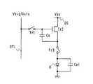
ここで図10は、特開2007−310311号公報に開示の画像表示装置を示すブロック図である。この画像表示装置1は、ガラス等の絶縁基板に表示部2が作成される。画像表示装置1は、この表示部2の周囲に信号線駆動回路3及び走査線駆動回路4が作成される。 Here, FIG. 10 is a block diagram showing an image display device disclosed in Japanese Patent Application Laid-Open No. 2007-310311. In the
ここで表示部2は、画素回路5をマトリックス状に配置して形成され、画素回路5に設けられた有機EL素子により画素(PIX)6が形成される。なおカラー画像の画像表示装置では、赤色、緑色及び青色による複数のサブ画素により1つの画素が構成されることから、カラー画像の画像表示装置の場合、表示部2は、赤色、緑色及び青色のサブ画素をそれぞれ構成する赤色用、緑色用及び青色用の画素回路5を順次配置して構成される。 Here, the
信号線駆動回路3は、表示部2に設けられた信号線DTLに信号線用の駆動信号Ssigを出力する。より具体的に、信号線駆動回路3は、データスキャン回路3Aにおいて、ラスタ走査順に入力される画像データD1を順次ラッチして画像データD1を信号線DTLに振り分けた後、それぞれディジタルアナログ変換処理する。信号線駆動回路3は、このディジタルアナログ変換結果を処理して駆動信号Ssigを生成する。これにより画像表示装置1は、例えばいわゆる線順次により各画素回路5の階調を設定する。 The signal line drive circuit 3 outputs a drive signal Ssig for the signal line to the signal line DTL provided in the
走査線駆動回路4は、表示部2に設けられた書込信号用の走査線WSL及び電源用の走査線DSLにそれぞれ書込信号WS及び駆動信号DSを出力する。ここで書込信号WSは、各画素回路5に設けられた書込トランジスタをオンオフ制御する信号である。また駆動信号DSは、各画素回路5に設けられた駆動トランジスタのドレイン電圧を制御する信号である。走査線駆動回路4は、それぞれライトスキャン回路(WSCN)4A及びドライブスキャン回路(DSCN)4Bにおいて、所定のサンプリングパルスSPをクロックCKで処理して書込信号WS及び駆動信号DSを生成する。 The scanning
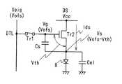
図11は、画素回路5の構成を詳細に示す接続図である。画素回路5は、有機EL素子8のカソードが所定の負側電圧に設定され、この図11の例ではこの負側電圧がアースラインの電圧に設定される。画素回路5は、有機EL素子8のアノードが駆動トランジスタTr2のソースに接続される。なお駆動トランジスタTr2は、例えばTFTによるNチャンネル型トランジスタである。画素回路5は、この駆動トランジスタTr2のドレインが電源用の走査線DSLに接続され、この走査線DSLに走査線駆動回路4から電源用の駆動信号DSが供給される。これらにより画素回路5は、ソースフォロワ回路構成の駆動トランジスタTr2を用いて有機EL素子8を電流駆動する。 FIG. 11 is a connection diagram showing the configuration of the
画素回路5は、この駆動トランジスタTr2のゲート及びソース間に保持容量Csが設けられ、書込信号WSによりこの保持容量Csのゲート側端電圧が駆動信号Ssigの電圧に設定される。その結果、画素回路5は、駆動信号Ssigに応じたゲートソース間電圧Vgsにより駆動トランジスタTr2で有機EL素子8を電流駆動する。なおここでこの図11において、容量Celは、有機EL素子8の浮遊容量である。また以下において、容量Celは、保持容量Csに比して十分に容量が大きいものとし、駆動トランジスタTr2のゲートノードの寄生容量は、保持容量Csに対して十分に小さいものとする。 In the
すなわち画素回路5は、書込信号WSによりオンオフ動作する書込トランジスタTr1を介して、駆動トランジスタTr2のゲートが信号線DTLに接続される。なおここで書込トランジスタTr1は、例えばTFTによるNチャンネル型トランジスタである。ここで信号線駆動回路3は、階調設定用電圧Vsig及びしきい値電圧の補正用電圧Vofsを所定のタイミングで切り換えて駆動信号Ssigを出力する。ここでしきい値電圧補正用の固定電圧Vofsは、駆動トランジスタTr2のしきい値電圧のばらつき補正に使用する固定電圧である。また階調設定用電圧Vsigは、有機EL素子8の発光輝度を指示する電圧であり、階調電圧Vinにしきい値電圧補正用の固定電圧Vofsを加算した電圧である。また階調電圧Vinは、有機EL素子8の発光輝度に対応する電圧である。階調電圧Vinは、各信号線DTLに振り分けた画像データD1をそれぞれディジタルアナログ変換処理して信号線DTL毎に生成される。 That is, in the
画素回路5は、図12に示すように、有機EL素子8を発光させる発光期間の間、書込信号WSにより書込トランジスタTr1がオフ状態に設定される(図12(A))。また画素回路5は、発光期間の間、電源用の駆動信号DSによって駆動トランジスタTr2に電源電圧Vccが供給される(図12(B))。これにより画素回路5は、図13に示すように、発光期間の間、保持容量Csの端子間電圧である駆動トランジスタTr2のゲートソース間電圧Vgs(図12(D)及び(E))に応じた駆動電流Idsで有機EL素子8を発光させる。 In the
画素回路5は、発光期間が終了する時点t0で、電源用の駆動信号DSが所定の固定電圧Vssに立ち下げられる(図12(B))。ここでこの固定電圧Vssは、駆動トランジスタTr2のドレインをソースとして機能させるのに十分に低い電圧であって、かつ有機EL素子8のカソード電圧より低い電圧である。 In the
これにより画素回路5は、図14に示すように、駆動トランジスタTr2を介して、保持容量Csの有機EL素子8側端の蓄積電荷が走査線に流出する。その結果、画素回路5は、駆動トランジスタTr2のソース電圧Vsが電圧Vssに立ち下がり(図12(E))、有機EL素子8が発光を停止する。また画素回路5は、このソース電圧Vsの立ち下がりに連動して、駆動トランジスタTr2のゲート電圧Vgが低下する(図12(D))。 As a result, in the
なおより正確に説明すると、ドレイン電圧の固定電圧Vssへの立ち下げにより、駆動トランジスタTr2のゲート電圧Vgは、駆動トランジスタTr2のドレインゲート間電圧のしきい値電圧だけこの固定電圧Vssから下がった電圧に保持される。また駆動トランジスタTr2のソース電圧Vsは、直前の発光期間におけるゲートソース間電圧だけゲート電圧Vgから下がった電圧に保持される。 More precisely, due to the fall of the drain voltage to the fixed voltage Vss, the gate voltage Vg of the drive transistor Tr2 is a voltage that is lowered from the fixed voltage Vss by the threshold voltage of the drain-gate voltage of the drive transistor Tr2. Retained. Further, the source voltage Vs of the drive transistor Tr2 is held at a voltage lower than the gate voltage Vg by the gate-source voltage in the immediately preceding light emission period.
画素回路5は、続く所定の時点t1で、書込信号WSにより書込トランジスタTr1がオン状態に切り換えられ(図12(A))、駆動トランジスタTr2のゲート電圧Vgが信号線DTLに設定されたしきい値電圧補正用の固定電圧Vofsに設定される(図12(C)及び(D))。これにより画素回路5は、図15に示すように、駆動トランジスタTr2のゲートソース間電圧Vgsがほぼ電圧Vofs−Vssに設定される。ここで画素回路5は、電圧Vofs、Vssの設定により、この電圧Vofs−Vssが駆動トランジスタTr2のしきい値電圧Vthより大きな電圧に設定される。 In the
その後、画素回路5は、時点t2で駆動信号DSにより駆動トランジスタTr2のドレイン電圧が電源電圧Vccに立ち上げられる(図12(B))。これにより画素回路5は、図16に示すように、駆動トランジスタTr2を介して保持容量Csの有機EL素子8側端に電源Vccから充電電流Idsが流入する。その結果、画素回路5は、保持容量Csの有機EL素子8側端の電圧Vsが徐々に上昇する。なおこの場合、画素回路5において、駆動トランジスタTr2を介して有機EL素子8に流入する電流Idsは、有機EL素子8の容量Celと保持容量Csの充電にのみ使用され、その結果、有機EL素子8を発光させることなく、単に駆動トランジスタTr2のソース電圧Vsのみが上昇することになる。 Thereafter, the
ここで画素回路5は、保持容量Csの端子間電圧が駆動トランジスタTr2のしきい値電圧Vthとなると、駆動トランジスタTr2を介した充電電流Idsの流入が停止することになる。従ってこの場合、この駆動トランジスタTr2のソース電圧Vsの上昇は、保持容量Csの両端電位差が駆動トランジスタTr2のしきい値電圧Vthとなると、停止することになる。これにより画素回路5は、駆動トランジスタTr2を介して保持容量Csの端子間電圧を放電させ、保持容量Csの端子間電圧を駆動トランジスタTr2のしきい値電圧Vthに設定する。 Here, when the inter-terminal voltage of the storage capacitor Cs becomes the threshold voltage Vth of the drive transistor Tr2, the
画素回路5は、保持容量Csの端子間電圧を駆動トランジスタTr2のしきい値電圧Vthに設定するのに十分な時間が経過して時点t3になると、図17に示すように、書込信号WSにより書込トランジスタTr1がオフ状態に切り換えられる(図12(A))。続いて図18に示すように、信号線DTLの電圧が階調設定用電圧Vsig(=Vin+Vofs)に設定される。 When a time sufficient to set the inter-terminal voltage of the storage capacitor Cs to the threshold voltage Vth of the drive transistor Tr2 has elapsed and the time point t3 has elapsed, the
画素回路5は、続く時点t4で書込トランジスタTr1がオン状態に設定される(図12(A))。これにより画素回路5は、図19に示すように、駆動トランジスタTr2のゲート電圧Vgが階調設定用電圧Vsigに設定され、駆動トランジスタTr2のゲートソース間電圧Vgsは、階調電圧Vinに駆動トランジスタTr2のしきい値電圧Vthを加算した電圧に設定される。これにより画素回路5は、駆動トランジスタTr2のしきい値電圧Vthのばらつきを有効に回避して有機EL素子8を駆動することができ、有機EL素子8の発光輝度のばらつきによる画質劣化を防止することができる。 In the
画素回路5は、この駆動トランジスタTr2のゲート電圧Vgを階調設定用電圧Vsigに設定する際に、駆動トランジスタTr2のドレイン電圧を電源電圧Vccに保持した状態で、一定期間の間、駆動トランジスタTr2のゲートが信号線DTLに接続される。これにより画素回路5は、併せて駆動トランジスタTr2の移動度μのばらつきが補正される。 When the gate voltage Vg of the drive transistor Tr2 is set to the gradation setting voltage Vsig, the
すなわち保持容量Csの端子間電圧を駆動トランジスタTr2のしきい値電圧Vthに設定した状態で、書込トランジスタTr1をオン状態に設定して駆動トランジスタTr2のゲートを信号線DTLに接続した場合、駆動トランジスタTr2のゲート電圧Vgは、固定電圧Vofsから徐々に上昇して階調設定用電圧Vsigに設定される。 That is, when the inter-terminal voltage of the storage capacitor Cs is set to the threshold voltage Vth of the drive transistor Tr2, the write transistor Tr1 is set to the on state and the gate of the drive transistor Tr2 is connected to the signal line DTL. The gate voltage Vg of the transistor Tr2 gradually rises from the fixed voltage Vofs and is set to the gradation setting voltage Vsig.
ここで画素回路5は、この駆動トランジスタTr2のゲート電圧Vgの立ち上がりに要する書込時定数が、駆動トランジスタTr2によるソース電圧Vsの立ち上がりに要する時定数に比して短くなるように設定される。 Here, the
この場合、書込トランジスタTr1がオン動作すると、駆動トランジスタTr2のゲート電圧Vgは、速やかに階調設定用電圧Vsig(Vofs+Vin)に立ち上がることになる。このゲート電圧Vgの立ち上がり時、有機EL素子8の容量Celが保持容量Csに比して十分に大きければ、駆動トランジスタTr2のソース電圧Vsは変動しないことになる。 In this case, when the write transistor Tr1 is turned on, the gate voltage Vg of the drive transistor Tr2 quickly rises to the gradation setting voltage Vsig (Vofs + Vin). When the gate voltage Vg rises, if the capacitance Cel of the
しかしながら駆動トランジスタTr2のゲートソース間電圧Vgsがしきい値電圧Vthより増大すると、駆動トランジスタTr2を介して電源Vccから電流Idsが流入し、駆動トランジスタTr2のソース電圧Vsが徐々に上昇することになる。その結果、画素回路5は、保持容量Csの端子間電圧が駆動トランジスタTr2により放電し、ゲートソース間電圧Vgsの上昇速度が低下することになる。 However, when the gate-source voltage Vgs of the drive transistor Tr2 increases from the threshold voltage Vth, the current Ids flows from the power supply Vcc via the drive transistor Tr2, and the source voltage Vs of the drive transistor Tr2 gradually increases. . As a result, in the
この端子間電圧の放電速度は、駆動トランジスタTr2の能力に応じて変化する。より具体的には、駆動トランジスタTr2の移動度μが大きい場合程、放電速度は、早くなる。 The discharge rate of the inter-terminal voltage changes according to the capability of the drive transistor Tr2. More specifically, the higher the mobility μ of the drive transistor Tr2, the faster the discharge rate.
その結果、画素回路5は、移動度μが大きい駆動トランジスタTr2程、保持容量Csの端子間電圧が低下するように設定され、移動度のばらつきによる発光輝度のばらつきが補正される。なおこの移動度μの補正に係る端子間電圧の低下分を図12、図19及び図20ではΔVで示す。 As a result, the
画素回路5は、この移動度の補正期間が経過すると、時点t5で書込信号WSが立ち下げられる。その結果、画素回路5は、発光期間が開始し、図20に示すように、保持容量Csの端子間電圧に応じた駆動電流Idsにより有機EL素子8を発光させる。なお画素回路5は、発光期間が開始すると、いわゆるブートストラップ回路により駆動トランジスタTr2のゲート電圧Vg及びソース電圧Vsが上昇する。図20におけるVelは、この上昇分の電圧である。 When the mobility correction period elapses, the
これらにより画素回路5は、時点t0から時点t2までの駆動トランジスタTr2のゲート電圧を電圧Vssに立ち下げている期間で、駆動トランジスタTr2のしきい値電圧を補正する処理の準備を実行する。また続く時点t2から時点t3までの期間で、保持容量Csの端子間電圧を駆動トランジスタTr2のしきい値電圧Vthに設定して、駆動トランジスタTr2のしきい値電圧を補正する。また時点t4から時点t5までの期間で、駆動トランジスタTr2の移動度を補正すると共に、階調設定用電圧Vsigをサンプリングする。 As a result, the
また特開2007−133284号公報には、駆動トランジスタTr2のしきい値電圧のばらつきを補正する処理を複数回に分けて実行する構成が提案されている。この特開2007−133284号公報に開示の構成によれば、高精度化して画素回路の階調設定に割り当てる時間が短くなった場合でも、しきい値電圧のばらつき補正に十分な時間を割り当てることができる。従って高精度化した場合でも、しきい値電圧のばらつきによる画質劣化を防止することができる。 Japanese Patent Laid-Open No. 2007-133284 proposes a configuration in which the process of correcting the variation in threshold voltage of the drive transistor Tr2 is executed in a plurality of times. According to the configuration disclosed in Japanese Patent Application Laid-Open No. 2007-133284, even when the time allocated to the gradation setting of the pixel circuit is shortened with high accuracy, sufficient time is allocated for correcting the variation in threshold voltage. Can do. Therefore, even when the accuracy is improved, it is possible to prevent image quality deterioration due to variations in threshold voltage.
従って特開2007−310311号公報に開示の手法に、特開2007−133284号公報に開示の手法を適用すると、簡易な構成により、高精度化した場合にあっても高い画質を維持することが可能な表示装置を得ることができると考えられる。 Therefore, when the technique disclosed in Japanese Patent Laid-Open No. 2007-133284 is applied to the technique disclosed in Japanese Patent Laid-Open No. 2007-310311, it is possible to maintain high image quality with a simple configuration even when the accuracy is improved. It is thought that possible display devices can be obtained.
図21は、図12との対比により、特開2007−310311号公報に開示の手法に、特開2007−133284号公報に開示の手法を適用した場合に考えられる画素回路のタイムチャートである。 FIG. 21 is a time chart of a pixel circuit conceivable when the method disclosed in Japanese Patent Application Laid-Open No. 2007-133284 is applied to the method disclosed in Japanese Patent Application Laid-Open No. 2007-310311 in comparison with FIG.
この場合、信号線DTLには、しきい値電圧補正用の固定電圧Vofsを間に挟んで、信号線DTLに接続された各画素回路5の階調設定用電圧Vsigが出力される。画素回路5は、この信号線DTLの駆動に対応して書込信号WSが間欠的に立ち上げられ、複数の期間で、保持容量Csの端子間電圧を駆動トランジスタTr2を介して放電させる。これによりこの図21の例では、駆動トランジスタTr2のしきい値電圧のばらつき補正を複数回の期間に分けて実行する。なおこの図21において、VDは、垂直同期信号である。 In this case, the gradation setting voltage Vsig of each
また特開2006−338042号公報には、電流駆動により有機EL素子の発光輝度を設定する構成が開示されている。
ところで図11の構成では、駆動トランジスタTr2のドレイン電圧を所定電圧Vssに立ち下げることにより、有機EL素子8の発光を停止させる。その結果、有機EL素子8の発光を停止している期間の間、有機EL素子8は、逆バイアスの状態に保持される。ここで有機EL素子は、逆バイアスの状態に保持されると、逆バイアスの大きさ、時間により破壊する場合がある。 By the way, in the configuration of FIG. 11, the emission of the
これにより図11の構成では、有機EL素子8が破壊して滅点が発生する恐れがあった。なお図11の構成では、この所定電圧Vssを高くすることにより、有機EL素子8に印加される逆バイアスの量を低減して有機EL素子8の破壊を防止することができる。しかしながら電圧Vssを高くすると、保持容量Csの端子間電圧を駆動トランジスタTr2のしきい値電圧以上の電圧に設定することが困難になり、結局、駆動トランジスタTr2のしきい値電圧のばらつきを補正できなくなる。 Accordingly, in the configuration of FIG. 11, the
本発明は以上の点を考慮してなされたもので、逆バイアスによる有機EL素子の破壊を有効に回避して、駆動トランジスタのしきい値電圧のばらつきを補正することができる画像表示装置を提案しようとするものである。 The present invention has been made in consideration of the above points, and proposes an image display device capable of effectively avoiding the destruction of the organic EL element due to the reverse bias and correcting the variation in the threshold voltage of the driving transistor. It is something to try.
上記の課題を解決するため請求項1の発明は、画像表示装置に適用して、画素回路をマトリックス状に配置して表示部が形成され、前記画素回路は、発光素子と、スイッチ用トランジスタと、前記スイッチ用トランジスタを介して、ゲートソース間電圧に応じた駆動電流により前記発光素子を電流駆動する駆動トランジスタと、前記ゲートソース間電圧を保持する保持容量と、信号線の電圧により前記保持容量の端子電圧を設定する書込トランジスタとを少なくとも有し、前記発光素子を発光させる発光期間と、前記発光素子の発光を停止させる非発光期間とを交互に繰り返し、前記非発光期間において、前記保持容量の端子間電圧を前記駆動トランジスタのしきい値電圧以上の電圧に設定した後、前記駆動トランジスタのしきい値電圧に応じた電圧に設定し、続いて前記保持容量の端子電圧を前記信号線の電圧に設定して、続く前記発光期間における前記発光素子の発光輝度を設定し、前記非発光期間において、前記スイッチ用トランジスタをオフ状態に設定する。 In order to solve the above problems, the invention of
請求項1の構成により、非発光期間、スイッチ用トランジスタをオフ状態に設定すれば、駆動トランジスタと発光素子とを切り離して、保持容量の端子間電圧を駆動トランジスタのしきい値電圧以上の電圧に設定する処理等を実行することができる。従ってこの処理等における逆バイアスが発光素子に印加されないようにすることができる。 According to the configuration of the first aspect, when the switching transistor is set to the off state during the non-light emitting period, the driving transistor and the light emitting element are separated, and the voltage across the storage capacitor is set to a voltage equal to or higher than the threshold voltage of the driving transistor. A setting process or the like can be executed. Accordingly, it is possible to prevent the reverse bias in this processing or the like from being applied to the light emitting element.
本発明によれば、逆バイアスによる有機EL素子の破壊を有効に回避して、駆動トランジスタのしきい値電圧のばらつきを補正することができる。 According to the present invention, it is possible to effectively avoid the destruction of the organic EL element due to the reverse bias and correct the variation in the threshold voltage of the driving transistor.
以下、適宜図面を参照しながら本発明の実施例を詳述する。 Hereinafter, embodiments of the present invention will be described in detail with reference to the drawings as appropriate.
(1)実施例1の構成
図1は、図11との対比により本発明の実施例1の画像表示装置に適用される画素回路を示す接続図であり、図2は、この画素回路を簡略化して示す接続図である。画素回路25は、駆動トランジスタTr2と有機EL素子8の間に、カットオフ信号CutOFFによりオンオフ動作してスイッチ回路として機能するスイッチ用トランジスタTr3が設けられる。この実施例の画像表示装置21は、図3に示すように、この画素回路25がマトリックス状に配置されて表示部22が形成される。画像表示装置21は、このスイッチ用トランジスタTr3の制御に関する構成が異なる点を除いて、図11について上述した画像表示装置1と同一に構成される。(1) Configuration of
すなわちこの画像表示装置21において(図1)、信号線駆動回路23は、データスキャン回路23Aにより各画素回路25の階調設定用電圧Vsigを生成し、しきい値電圧補正用の固定電圧Vofsを間に挟んで、この階調設定用電圧Vsigを順次信号線DTLに出力する。走査線駆動回路24は、ライトスキャン回路24A、ドライブスキャン回路24B及びカットオフスキャン回路24Cからそれぞれ書込信号WS、駆動信号DS及びカットオフ信号CutOFFを出力する。 That is, in this image display device 21 (FIG. 1), the signal
図4に示すように、画像表示装置21は、カットオフ信号CutOFFにより、非発光期間の間、スイッチ用トランジスタTr3がオフ状態に設定され、これにより有機EL素子8の逆バイアスを有効に回避する(図4(E))。 As shown in FIG. 4, in the
すなわち画素回路25は、発光期間の間、図5に示すように、書込トランジスタTr1、スイッチ用トランジスタTr3がそれぞれオフ状態及びオン状態に設定され、駆動トランジスタTr2に電源電圧Vccが供給される(図4(A)〜(E))。これにより画素回路25は、保持容量Csの端子間電圧に応じた駆動電流Idsで有機EL素子8を駆動する。 That is, in the
画素回路25は、発光期間が終了する時点t0で、図6に示すように、駆動トランジスタTr2のドレイン電圧が固定電位Vssに立ち下げられると共に、スイッチ用トランジスタTr3がオフ状態に設定される。これにより画素回路25は、保持容量Csの有機EL素子8側端の蓄積電荷が駆動トランジスタTr2を介して走査線に流出し、駆動トランジスタTr2のゲート電圧Vg及びソース電圧Vsが立ち下がる(図4(G)及び(H))。このときスイッチ用トランジスタTr3がオフ状態に設定されていることから、有機EL素子8は、浮遊容量Celの蓄積電荷が有機EL素子8を介して放電し、この放電により端子間電圧が有機EL素子8のしきい値電圧Vth ELにまで低下する。その結果、有機EL素子8は、アノード電圧VAが、カソード電圧にしきい値電圧Vth ELを加算した電圧に保持される(図4(F))。 In the
画素回路25は、続いて信号線DTLがしきい値電圧補正用の固定電圧Vofsに保持されている期間で、書込信号WSにより書込トランジスタTr1がオン状態に設定される。これにより画素回路25は、保持容量Csの端子間電圧が駆動トランジスタTr2のしきい値電圧Vth以上の電圧に設定される。 In the
画素回路25は、続いて駆動トランジスタTr2のドレイン電圧が電源電圧Vccに立ち上げられると共に、信号線DTLがしきい値電圧補正用の固定電圧Vofsに保持されている期間の間、書込トランジスタTr1がオン状態に設定される。これにより図7に示すように、画素回路25は、複数回の期間に分けて、図7に示すように、保持容量Csの端子間電圧が駆動トランジスタTr2のしきい値電圧Vthに設定される。 In the
画素回路25は、続いて信号線DTLが当該画素回路25の階調設定用電圧Vsigに保持されている時点t2で、書込トランジスタTr1がオン状態に設定され、これにより保持容量Csの端子電圧が階調設定用電圧Vsigに設定される。また一定の時間だけ経過すると、書込トランジスタTr1がオフ状態に設定され、これにより移動度のばらつきを補正して階調設定用電圧Vsigが保持容量Csにサンプルホールドされる。 In the
その結果、画素回路25は、図8に示すように、保持容量Csの端子間電圧に応じた駆動電流Idsにより有機EL素子8を発光させる。 As a result, as shown in FIG. 8, the
なお図9は、この画素回路25のレイアウトを示す平面図である。この図9は、有機EL素子8のアノード電極から上層の部材を除去して基板側を見て示す平面図である。この図9では、各層の配線パターンをそれぞれハッチングの相違により示す。また円形の印により層間のコンタクトを示す。またこの円形の印の内側にコンタクト先の配線パターンに割り当てたハッチングを設け、層間の接続関係を示す。 FIG. 9 is a plan view showing the layout of the
画素回路25は、例えばガラスによる絶縁基板上に配線パターン材料層を堆積した後、この配線パターン材料層をエッチング処理して第1配線が作成される。画素回路5は、続いてゲート酸化膜が作成された後、ポリシリコン膜による中間配線層が作成される。画素回路5は、続いてチャンネル保護層等が作成された後、不純物のドープによりトランジスタTr1〜Tr3が作成される。 In the
画素回路25は、続いて配線パターン材料層を堆積した後、この配線パターン材料層をエッチング処理して第2配線が作成される。画素回路25は、第2配線により電源用の走査線DSL及び書込信号用の走査線WSLが作成される。また電源用の走査線DSLが書込信号用の走査線WSLに比して幅広に作成される。また画素回路25は、可能な限り第2配線により信号線DTLが作成される。具体的に、画素回路25は、走査線DSL及びWSLと交差する部位に限って、第1配線により信号線DTLが作成され、残りの信号線DTLが第2配線により作成される。またその結果、信号線DTLは、走査線DSL及びWSLと交差する部位を間に挟んで、第1配線及び第2配線を接続するコンタクトがそれぞれ設けられる。 The
(2)実施例の動作
以上の構成において、この画像表示装置21では、信号線駆動回路23において、順次入力される画像データD1が信号線DTLに振り分けられた後、アナログディジタル変換処理される。これにより画像表示装置21では、信号線DTLに接続された各画素の階調を指示する階調電圧Vinが信号線DTL毎に作成される。画像表示装置21では、走査線駆動回路24による表示部の駆動により、表示部2を構成する各画素回路5に例えば線順次によりこの階調電圧Vinが設定される。また各画素回路5では、この階調電圧Vinに応じた発光輝度によりそれぞれ有機EL素子8が発光する(図1)。これにより画像表示装置21では、画像データD1に応じた画像を表示部2で表示することができる。(2) Operation of Embodiment In the above configuration, in the
より具体的に、画素回路5においては、ソースフォロワ回路構成の駆動トランジスタTr2により有機EL素子8が電流駆動される。画素回路5においては、この駆動トランジスタTr2のゲートソース間に設けられた保持容量Csのゲート側端の電圧が階調電圧Vinに応じた電圧Vsigに設定される。これにより画像表示装置21では、画像データD1に応じた発光輝度により有機EL素子8を発光させて所望の画像を表示する。 More specifically, in the
しかしながらこれら画素回路5に適用される駆動トランジスタTr2は、しきい値電圧Vthのばらつきが大きい欠点がある。その結果、画像表示装置21では、単に保持容量Csのゲート側端電圧を階調電圧Vinに応じた電圧Vsigに設定したのでは、駆動トランジスタTr2のしきい値電圧Vthのばらつきにより有機EL素子8の発光輝度がばらつき、画質が劣化する。 However, the driving transistor Tr2 applied to the
そこで画像表示装置21では、事前に、保持容量Csの有機EL素子8側端電圧を立ち下げた後、書込トランジスタTr1を介して駆動トランジスタTr2のゲート電圧がしきい値電圧補正用の固定電圧Vofsに設定される(図2)。これにより画像表示装置21では、保持容量Csの端子間電圧が駆動トランジスタTr2のしきい値電圧Vth以上に設定される。またその後、駆動トランジスタTr2を介して、この保持容量Csの端子間電圧が放電される。これらの一連の処理により、画像表示装置21では、保持容量Csの端子間電圧が、事前に、駆動トランジスタTr2のしきい値電圧Vthに設定される。 Therefore, in the
その後、画像表示装置21では、階調電圧Vinに固定電圧Vofsを加算した階調設定用電圧Vsigが駆動トランジスタTr2のゲート電圧に設定される。これにより画像表示装置21では、駆動トランジスタTr2のしきい値電圧Vthのばらつきによる画質劣化を防止することができる。 Thereafter, in the
また一定時間の間、駆動トランジスタTr2に電源を供給した状態で、駆動トランジスタTr2のゲート電圧を階調設定用電圧Vsigに保持することにより、駆動トランジスタTr2の移動度のばらつきによる画質劣化を防止することができる。 In addition, the gate voltage of the drive transistor Tr2 is held at the gradation setting voltage Vsig while power is supplied to the drive transistor Tr2 for a certain time, thereby preventing image quality deterioration due to variation in mobility of the drive transistor Tr2. be able to.
しかしながら高解像度化等により、駆動トランジスタTr2を介した保持容量Csの端子間電圧の放電に、十分な時間を割り当てることが困難な場合も発生する。この場合、画像表示装置では、十分に精度良く、保持容量Csの端子間電圧を駆動トランジスタTr2のしきい値電圧Vthに設定できなくなる。その結果、十分に駆動トランジスタTr2のしきい値電圧Vthのばらつきを補正できなくなる問題がある。 However, due to high resolution and the like, it may be difficult to allocate sufficient time for discharging the voltage across the storage capacitor Cs via the drive transistor Tr2. In this case, the image display device cannot set the voltage across the storage capacitor Cs to the threshold voltage Vth of the drive transistor Tr2 with sufficient accuracy. As a result, there is a problem that variations in the threshold voltage Vth of the drive transistor Tr2 cannot be sufficiently corrected.
そこでこの実施例では、駆動トランジスタTr2を介した保持容量Csの端子間電圧の放電が、複数回の期間で実行される。これにより駆動トランジスタTr2を介した保持容量Csの端子間電圧の放電に、十分な時間を割り当て、高解像度化した場合でも、十分に駆動トランジスタTr2の移動度のばらつきを補正する。 Therefore, in this embodiment, the discharge of the voltage across the storage capacitor Cs via the drive transistor Tr2 is executed in a plurality of periods. As a result, even when sufficient time is allocated to discharge the inter-terminal voltage of the storage capacitor Cs via the drive transistor Tr2 and the resolution is increased, the variation in mobility of the drive transistor Tr2 is sufficiently corrected.
しかしながらこのようにして駆動トランジスタTr2のしきい値電圧のばらつき補正を実行する場合、有機EL素子8が逆バイアスされることになり、有機EL素子8の破壊が心配される。 However, when the variation correction of the threshold voltage of the drive transistor Tr2 is executed in this way, the
そこでこの実施例では、有機EL素子8と駆動トランジスタTr2との間に、スイッチ用トランジスタTr3が設けられ、非発光期間の間、このスイッチ用トランジスタTr3がオフ状態に設定される。これにより画像表示装置21では、駆動トランジスタTr2と有機EL素子8とを切り離して、一連の駆動トランジスタTr2のしきい値電圧のばらつきを補正する処理を実行することができる。従って、有機EL素子8の逆バイアスを有効に回避して、駆動トランジスタのしきい値電圧のばらつきを補正することができる。 Therefore, in this embodiment, the switching transistor Tr3 is provided between the
(3)実施例の効果
以上の構成によれば、駆動トランジスタと発光素子との間にスイッチ用トランジスタを配置し、非発光期間の間、このスイッチ用トランジスタをオフ状態に設定することにより、逆バイアスによる有機EL素子の破壊を有効に回避して、駆動トランジスタのしきい値電圧のばらつきを補正することができる。(3) Effects of the embodiment According to the above configuration, the switching transistor is disposed between the driving transistor and the light emitting element, and the switching transistor is set to the off state during the non-light emitting period, thereby It is possible to effectively avoid the destruction of the organic EL element due to the bias and correct the variation in the threshold voltage of the driving transistor.
なお上述の実施例においては、画素回路を2つのトランジスタで構成する画像表示装置に本発明を適用する場合について述べたが、本発明はこれに限らず、保持容量の有機EL素子側端の電圧を専用の回路構成により立ち下げてしきい値電圧のばらつき補正処理を開始する構成等にも広く適用することができる。 In the above-described embodiments, the case where the present invention is applied to an image display device in which a pixel circuit is configured by two transistors has been described. However, the present invention is not limited thereto, and the voltage at the organic EL element side end of the storage capacitor Can be widely applied to a configuration in which the threshold voltage variation correction processing is started by falling down with a dedicated circuit configuration.
また上述の実施例においては、駆動トランジスタを介した保持容量の端子間電圧の放電を複数回の期間で実行する場合について述べたが、本発明はこれに限らず、この放電の処理を1回の期間で実行する場合にも広く適用することができる。 In the above-described embodiment, the case where the discharge of the voltage across the storage capacitor via the drive transistor is performed in a plurality of periods has been described. However, the present invention is not limited to this, and this discharge process is performed once. The present invention can also be widely applied to the case where the process is executed in the period.
また上述の実施例においては、Nチャンネル型のトランジスタを駆動トランジスタに適用する場合について述べたが、本発明はこれに限らず、Pチャンネル型のトランジスタを駆動トランジスタに適用する画像表示装置等に広く適用することができる。 In the above-described embodiments, the case where the N-channel type transistor is applied to the driving transistor has been described. However, the present invention is not limited to this, and the present invention is widely applied to image display devices and the like that apply the P-channel type transistor to the driving transistor. Can be applied.
また上述の実施例においては、本発明を有機EL素子の画像表示装置に適用する場合について述べたが、本発明はこれに限らず、電流駆動型の各種自発光素子による画像表示装置に広く適用することができる。 Further, in the above-described embodiments, the case where the present invention is applied to an image display device of an organic EL element has been described. However, the present invention is not limited to this, and is widely applied to image display devices using various current-driven self-luminous elements. can do.
本発明は、画像表示装置に関し、例えば有機EL素子によるアクティブマトリックス型の画像表示装置に適用することができる。 The present invention relates to an image display device, and can be applied to, for example, an active matrix image display device using organic EL elements.
1、21……画像表示装置、2、22……表示部、3、23……信号線駆動回路、4、24……走査線駆動回路、5、25……画素回路、8……有機EL素子、Tr1〜Tr3……トランジスタ、Cs……保持容量
1, 21... Image display device, 2, 22... Display unit, 3, 23... Signal line drive circuit, 4, 24... Scan line drive circuit, 5, 25. Element, Tr1 to Tr3 ... Transistor, Cs ... Retention capacitance
Claims (2)
Translated fromJapanese前記画素回路は、
発光素子と、
スイッチ用トランジスタと、
前記スイッチ用トランジスタを介して、ゲートソース間電圧に応じた駆動電流により前記発光素子を電流駆動する駆動トランジスタと、
前記ゲートソース間電圧を保持する保持容量と、
信号線の電圧により前記保持容量の端子電圧を設定する書込トランジスタとを少なくとも有し、
前記発光素子を発光させる発光期間と、前記発光素子の発光を停止させる非発光期間とを交互に繰り返し、
前記非発光期間において、
前記保持容量の端子間電圧を前記駆動トランジスタのしきい値電圧以上の電圧に設定した後、前記駆動トランジスタのしきい値電圧に応じた電圧に設定し、
続いて前記保持容量の端子電圧を前記信号線の電圧に設定して、続く前記発光期間における前記発光素子の発光輝度を設定し、
前記非発光期間において、前記スイッチ用トランジスタをオフ状態に設定する
画像表示装置。A display unit is formed by arranging pixel circuits in a matrix,
The pixel circuit includes:
A light emitting element;
A switching transistor;
A drive transistor for driving the light emitting element with a drive current according to a gate-source voltage via the switch transistor;
A holding capacitor for holding the gate-source voltage;
And at least a write transistor that sets a terminal voltage of the storage capacitor by a voltage of a signal line,
A light emitting period for causing the light emitting element to emit light and a non-light emitting period for stopping the light emission of the light emitting element are alternately repeated,
In the non-light emission period,
After setting the voltage between the terminals of the storage capacitor to a voltage equal to or higher than the threshold voltage of the drive transistor, set the voltage according to the threshold voltage of the drive transistor,
Subsequently, the terminal voltage of the storage capacitor is set to the voltage of the signal line, the light emission luminance of the light emitting element in the subsequent light emission period is set,
An image display device that sets the switch transistor in an off state during the non-light emitting period.
請求項1に記載の画像表示装置。
By lowering the drain voltage of the drive transistor and setting the terminal voltage of the storage capacitor by the signal line through the write transistor, the voltage across the storage capacitor is changed to the threshold voltage of the drive transistor. The image display apparatus according to claim 1, wherein the voltage is set to the above voltage.
Priority Applications (4)
| Application Number | Priority Date | Filing Date | Title |
|---|---|---|---|
| JP2008144061AJP2009288734A (en) | 2008-06-02 | 2008-06-02 | Image display device |
| US12/453,162US8269697B2 (en) | 2008-06-02 | 2009-04-30 | Pixel circuit in image display device including a storage capacitor with the voltage more than the threshold voltage of the driving transistor by lowering a drain voltage of the driving transistor |
| KR1020090046261AKR101559370B1 (en) | 2008-06-02 | 2009-05-27 | Image display device |
| US13/597,491US9093024B2 (en) | 2008-06-02 | 2012-08-29 | Image display apparatus including a non-emission period lowering the gate and source voltage of the drive transistor |
Applications Claiming Priority (1)
| Application Number | Priority Date | Filing Date | Title |
|---|---|---|---|
| JP2008144061AJP2009288734A (en) | 2008-06-02 | 2008-06-02 | Image display device |
Publications (1)
| Publication Number | Publication Date |
|---|---|
| JP2009288734Atrue JP2009288734A (en) | 2009-12-10 |
Family
ID=41379152
Family Applications (1)
| Application Number | Title | Priority Date | Filing Date |
|---|---|---|---|
| JP2008144061APendingJP2009288734A (en) | 2008-06-02 | 2008-06-02 | Image display device |
Country Status (3)
| Country | Link |
|---|---|
| US (2) | US8269697B2 (en) |
| JP (1) | JP2009288734A (en) |
| KR (1) | KR101559370B1 (en) |
Cited By (3)
| Publication number | Priority date | Publication date | Assignee | Title |
|---|---|---|---|---|
| JP2012108192A (en)* | 2010-11-15 | 2012-06-07 | Toshiba Mobile Display Co Ltd | Display device and driving method of display device |
| WO2019123288A1 (en)* | 2017-12-22 | 2019-06-27 | 株式会社半導体エネルギー研究所 | Display device and electronic equipment |
| US10957720B2 (en) | 2017-11-09 | 2021-03-23 | Semiconductor Energy Laboratory Co., Ltd. | Semiconductor device, display device, and electronic device |
Families Citing this family (11)
| Publication number | Priority date | Publication date | Assignee | Title |
|---|---|---|---|---|
| JP2010049041A (en)* | 2008-08-22 | 2010-03-04 | Sony Corp | Image display device and driving method of the image display device |
| KR101117729B1 (en)* | 2009-12-17 | 2012-03-07 | 삼성모바일디스플레이주식회사 | Pixel circuit, and organic light emitting display and method for controlling a brightness thereof |
| JP2012137513A (en)* | 2010-12-24 | 2012-07-19 | Sony Corp | Signal processing device and display device |
| US10607542B2 (en) | 2013-12-31 | 2020-03-31 | Kunshan New Flat Panel Display Technology Center Co., Ltd. | Pixel circuit, pixel, and AMOLED display device comprising pixel and driving method thereof |
| CN104751777B (en)* | 2013-12-31 | 2017-10-17 | 昆山工研院新型平板显示技术中心有限公司 | Image element circuit, pixel and AMOLED display device and its driving method including the pixel |
| WO2015170614A1 (en) | 2014-05-07 | 2015-11-12 | ソニー株式会社 | Display device and electronic apparatus |
| KR102254074B1 (en)* | 2014-10-22 | 2021-05-21 | 엘지디스플레이 주식회사 | Data driver and organic light emitting diode display device using the same |
| KR102218653B1 (en)* | 2015-02-12 | 2021-02-23 | 삼성디스플레이 주식회사 | Display device compensating variation of power supply voltage |
| US11328678B2 (en) | 2017-04-28 | 2022-05-10 | Shenzhen China Star Optoelectronics Semiconductor Display Technology Co., Ltd. | Display panel, pixel driving circuit, and drving method thereof |
| US10825399B2 (en) | 2018-01-12 | 2020-11-03 | Shenzhen China Star Optoelectronics Semiconductor Display Technology Co., Ltd. | Display panel, pixel driving circuit, and drying method thereof |
| CN106960659B (en) | 2017-04-28 | 2019-09-27 | 深圳市华星光电半导体显示技术有限公司 | Display panel, pixel-driving circuit and its driving method |
Citations (2)
| Publication number | Priority date | Publication date | Assignee | Title |
|---|---|---|---|---|
| JP2007133284A (en)* | 2005-11-14 | 2007-05-31 | Sony Corp | Display device and method for driving same |
| JP2008170857A (en)* | 2007-01-15 | 2008-07-24 | Sony Corp | Display devices and driving method thereof |
Family Cites Families (23)
| Publication number | Priority date | Publication date | Assignee | Title |
|---|---|---|---|---|
| EP3716257B1 (en)* | 2001-09-07 | 2021-01-20 | Joled Inc. | El display panel, method of driving the same, and el display device |
| JP2006338042A (en) | 2001-09-21 | 2006-12-14 | Semiconductor Energy Lab Co Ltd | Light emitting device, and driving method of light emitting device |
| JP3899886B2 (en)* | 2001-10-10 | 2007-03-28 | 株式会社日立製作所 | Image display device |
| US7612749B2 (en) | 2003-03-04 | 2009-11-03 | Chi Mei Optoelectronics Corporation | Driving circuits for displays |
| JP2005099714A (en)* | 2003-08-29 | 2005-04-14 | Seiko Epson Corp | Electro-optical device, driving method of electro-optical device, and electronic apparatus |
| KR100637458B1 (en)* | 2004-05-25 | 2006-10-20 | 삼성에스디아이 주식회사 | Organic light emitting display panel |
| TW200620207A (en)* | 2004-07-05 | 2006-06-16 | Sony Corp | Pixel circuit, display device, driving method of pixel circuit, and driving method of display device |
| EP1825455A4 (en)* | 2004-11-16 | 2009-05-06 | Ignis Innovation Inc | System and driving method for active matrix light emitting device display |
| KR100805542B1 (en)* | 2004-12-24 | 2008-02-20 | 삼성에스디아이 주식회사 | Light-emitting display device and driving method thereof |
| JP4923410B2 (en)* | 2005-02-02 | 2012-04-25 | ソニー株式会社 | Pixel circuit and display device |
| KR100731741B1 (en)* | 2005-04-29 | 2007-06-22 | 삼성에스디아이 주식회사 | Organic light emitting device |
| JPWO2006121138A1 (en)* | 2005-05-11 | 2008-12-18 | パイオニア株式会社 | Active matrix display device |
| JP2007005646A (en) | 2005-06-24 | 2007-01-11 | Sony Corp | Semiconductor integrated circuit |
| JP2007108381A (en)* | 2005-10-13 | 2007-04-26 | Sony Corp | Display device and driving method of same |
| JP2007108378A (en)* | 2005-10-13 | 2007-04-26 | Sony Corp | Driving method of display device and display device |
| JP4692828B2 (en)* | 2006-03-14 | 2011-06-01 | カシオ計算機株式会社 | Display device and drive control method thereof |
| JP4240059B2 (en) | 2006-05-22 | 2009-03-18 | ソニー株式会社 | Display device and driving method thereof |
| JP2008032866A (en)* | 2006-07-27 | 2008-02-14 | Sony Corp | Display device and driving method of display device |
| JP2008051990A (en) | 2006-08-24 | 2008-03-06 | Sony Corp | Display device |
| JP2008083107A (en) | 2006-09-26 | 2008-04-10 | Sony Corp | Display device |
| JP5055963B2 (en) | 2006-11-13 | 2012-10-24 | ソニー株式会社 | Display device and driving method of display device |
| JP2008233123A (en)* | 2007-03-16 | 2008-10-02 | Sony Corp | Display device |
| JP4957696B2 (en)* | 2008-10-02 | 2012-06-20 | ソニー株式会社 | Semiconductor integrated circuit, self-luminous display panel module, electronic device, and power line driving method |
- 2008
- 2008-06-02JPJP2008144061Apatent/JP2009288734A/enactivePending
- 2009
- 2009-04-30USUS12/453,162patent/US8269697B2/enactiveActive
- 2009-05-27KRKR1020090046261Apatent/KR101559370B1/ennot_activeExpired - Fee Related
- 2012
- 2012-08-29USUS13/597,491patent/US9093024B2/enactiveActive
Patent Citations (2)
| Publication number | Priority date | Publication date | Assignee | Title |
|---|---|---|---|---|
| JP2007133284A (en)* | 2005-11-14 | 2007-05-31 | Sony Corp | Display device and method for driving same |
| JP2008170857A (en)* | 2007-01-15 | 2008-07-24 | Sony Corp | Display devices and driving method thereof |
Cited By (6)
| Publication number | Priority date | Publication date | Assignee | Title |
|---|---|---|---|---|
| JP2012108192A (en)* | 2010-11-15 | 2012-06-07 | Toshiba Mobile Display Co Ltd | Display device and driving method of display device |
| US10957720B2 (en) | 2017-11-09 | 2021-03-23 | Semiconductor Energy Laboratory Co., Ltd. | Semiconductor device, display device, and electronic device |
| WO2019123288A1 (en)* | 2017-12-22 | 2019-06-27 | 株式会社半導体エネルギー研究所 | Display device and electronic equipment |
| JPWO2019123288A1 (en)* | 2017-12-22 | 2021-01-21 | 株式会社半導体エネルギー研究所 | Display devices and electronic devices |
| US11100855B2 (en) | 2017-12-22 | 2021-08-24 | Semiconductor Energy Laboratory Co., Ltd. | Display device and electronic device |
| JP7278962B2 (en) | 2017-12-22 | 2023-05-22 | 株式会社半導体エネルギー研究所 | Displays and electronics |
Also Published As
| Publication number | Publication date |
|---|---|
| US20090295691A1 (en) | 2009-12-03 |
| US8269697B2 (en) | 2012-09-18 |
| KR20090125703A (en) | 2009-12-07 |
| US20120320029A1 (en) | 2012-12-20 |
| KR101559370B1 (en) | 2015-10-12 |
| US9093024B2 (en) | 2015-07-28 |
Similar Documents
| Publication | Publication Date | Title |
|---|---|---|
| JP2009288734A (en) | Image display device | |
| KR101589902B1 (en) | Self-Emission Display Device and Driving Method Thereof | |
| JP5157467B2 (en) | Self-luminous display device and driving method thereof | |
| JP2010060873A (en) | Image display device | |
| JP4826598B2 (en) | Image display device and driving method of image display device | |
| JP4967946B2 (en) | Display device and driving method of display device | |
| JP2009276460A (en) | Display device | |
| JP4780134B2 (en) | Image display device and driving method of image display device | |
| JP2006215275A (en) | Display apparatus | |
| JP5088294B2 (en) | Image display device and driving method of image display device | |
| JP2009258275A (en) | Display device and output buffer circuit | |
| US11270639B2 (en) | Pixel circuit and display device | |
| JP2008225019A (en) | Display device | |
| CN101656048B (en) | Image display device and driving method of image display device | |
| JP2010054564A (en) | Image display device and method for driving image display device | |
| JP5353066B2 (en) | Image display device and method of manufacturing image display device | |
| US8610647B2 (en) | Image display apparatus and method of driving the image display apparatus | |
| JP2009251486A (en) | Image display apparatus and method for manufacturing the same | |
| JP2006227237A (en) | Display device and display method | |
| JP2010060601A (en) | Image display apparatus and method for driving the same | |
| JP2013047830A (en) | Display device and electronic apparatus | |
| JP2010020034A (en) | Image display device | |
| JP2009058919A (en) | Display device, driving method of the same, and method for manufacturing the same | |
| JP2009031620A (en) | Display device and driving method of display device | |
| JP2008203387A (en) | Image display |
Legal Events
| Date | Code | Title | Description |
|---|---|---|---|
| A977 | Report on retrieval | Free format text:JAPANESE INTERMEDIATE CODE: A971007 Effective date:20100405 | |
| A131 | Notification of reasons for refusal | Free format text:JAPANESE INTERMEDIATE CODE: A131 Effective date:20100413 | |
| A521 | Request for written amendment filed | Free format text:JAPANESE INTERMEDIATE CODE: A523 Effective date:20100604 | |
| A02 | Decision of refusal | Free format text:JAPANESE INTERMEDIATE CODE: A02 Effective date:20101221 |