JP2009284426A - Da converting circuit and driving device for display - Google Patents
Da converting circuit and driving device for displayDownload PDFInfo
- Publication number
- JP2009284426A JP2009284426AJP2008136921AJP2008136921AJP2009284426AJP 2009284426 AJP2009284426 AJP 2009284426AJP 2008136921 AJP2008136921 AJP 2008136921AJP 2008136921 AJP2008136921 AJP 2008136921AJP 2009284426 AJP2009284426 AJP 2009284426A
- Authority
- JP
- Japan
- Prior art keywords
- voltage
- circuit
- reference voltage
- supplied
- block
- Prior art date
- Legal status (The legal status is an assumption and is not a legal conclusion. Google has not performed a legal analysis and makes no representation as to the accuracy of the status listed.)
- Pending
Links
Images


Landscapes
- Analogue/Digital Conversion (AREA)
- Liquid Crystal Display Device Control (AREA)
- Control Of Indicators Other Than Cathode Ray Tubes (AREA)
Abstract
Translated fromJapaneseDescription
Translated fromJapanese本発明は、デジタルデータに基づいたアナログ電圧を出力するDA変換回路、およびそれを使用した表示用駆動装置に関するものであり、特に、例えばロジックトランジスタなどの低い耐圧のトランジスタを構成可能な技術に関するものである。 The present invention relates to a DA converter circuit that outputs an analog voltage based on digital data, and a display driving device using the DA converter circuit, and more particularly to a technology capable of constructing a low breakdown voltage transistor such as a logic transistor. It is.
液晶表示装置における表示方式のうち、高精細な表示を行える方式としてスイッチング素子にTFT(Thin Film Transistor)を用いたアクティブマトリクス方式がある。アクティブマトリクス方式の液晶表示装置では、ゲートドライバから出力される走査信号によってTFTを1ラインずつ順次ONし、ON状態のTFTを通して、該TFTのドレインに接続された画素電極にソースドライバから駆動電圧を印加する。これにより、画素電極と対向電極との間の画素容量に電荷が蓄積されることで液晶において光透過率が変化し、表示が行なわれる。 Among display methods in a liquid crystal display device, there is an active matrix method using a TFT (Thin Film Transistor) as a switching element as a method capable of high-definition display. In an active matrix liquid crystal display device, TFTs are sequentially turned on line by line by a scanning signal output from a gate driver, and a drive voltage is applied from the source driver to the pixel electrode connected to the drain of the TFT through the TFT in the ON state. Apply. As a result, charges are accumulated in the pixel capacitance between the pixel electrode and the counter electrode, whereby the light transmittance is changed in the liquid crystal, and display is performed.
このような液晶表示装置において階調表示を行う場合、ソースドライバから出力される駆動電圧を、表示対象の画素の明るさに応じた階調表示電圧として与える方法がある。液晶にて表示を行うためには、一般的に10V以上の電圧を画素容量に与えることが必要とされるので、ソースドライバは、10V以上の駆動電圧を出力するために、10V以上の耐圧を持つことが必要とされる。 In the case of performing gradation display in such a liquid crystal display device, there is a method in which a driving voltage output from a source driver is given as a gradation display voltage corresponding to the brightness of a pixel to be displayed. In order to perform display with liquid crystal, it is generally necessary to apply a voltage of 10 V or more to the pixel capacitor. Therefore, the source driver has a withstand voltage of 10 V or more in order to output a driving voltage of 10 V or more. It is necessary to have.
ゲートドライバおよびソースドライバは、集積回路により作成される。集積回路に構成されるMOSトランジスタは、耐圧が低いものほど、サイズが小さくて済む。例えば、5V程度以下の耐圧のMOSトランジスタ(所謂、ロジックトランジスタと呼ばれる)と、10V程度以上の耐圧のMOSトランジスタ(所謂、中耐圧トランジスタと呼ばれる)とでトランジスタの構成面積を比較すると、耐圧やプロセスにもよるが、およそ10倍の差になる。 The gate driver and the source driver are created by an integrated circuit. A MOS transistor configured in an integrated circuit is smaller in size as the breakdown voltage is lower. For example, when comparing the configuration area of a transistor between a MOS transistor having a breakdown voltage of about 5 V or less (so-called logic transistor) and a MOS transistor having a breakdown voltage of about 10 V or more (so-called medium breakdown voltage transistor), the breakdown voltage and process Although it depends, it becomes a difference of about 10 times.
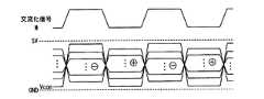
そこで、図17に示すような共通電極交流駆動が行われている。共通電極交流駆動とは、表示データに対応した液晶印加電圧の交流化と同じタイミングで共通電極(画素電極)を交流化することであり、10V程度を出力するソースドライバを5V耐圧の範囲内で動作させることができる。これにより、ソースドライバをロジックトランジスタで構成して、チップ面積を小さくするとともにコストを下げることが行われている。 Therefore, common electrode AC driving as shown in FIG. 17 is performed. The common electrode AC drive means that the common electrode (pixel electrode) is AC-converted at the same timing as the AC conversion of the liquid crystal applied voltage corresponding to the display data, and the source driver that outputs about 10V is within the range of 5V withstand voltage. It can be operated. As a result, the source driver is composed of logic transistors to reduce the chip area and reduce the cost.
また、上記共通電極交流駆動を行い、さらに回路規模を縮小する回路形式が、特許文献1に記載されている。 Further,
図18は、特許文献1に記載の従来のソースドライバ900の構成を示すブロック図である。 FIG. 18 is a block diagram showing a configuration of a
図18に示すように、ソースドライバ900は、入力ラッチ回路901、シフトレジスタ回路902、サンプリングメモリ回路903、ホールドメモリ回路904、レベルシフタ回路905、DA変換回路906、出力回路907、基準電圧発生回路908、およびセレクタ回路909を備えている。 As shown in FIG. 18, the
ソースドライバ900では、例えば、コントローラ(図示せず)からデジタル表示データDR・DG・DB(例えば各6ビット)が転送されてくると、入力ラッチ回路901が、該デジタル表示データDR・DG・DBを一旦ラッチした後、サンプリングメモリ回路903に出力する。なお、デジタル表示データDR・DG・DBは、それぞれ赤・緑・青に対応している。 In the
一方、ソースドライバ900では、コントローラから、デジタル表示データの転送を制御するためのスタートパルス信号SPとクロック信号CKとが、シフトレジスタ回路902に出力されている。シフトレジスタ回路902は、クロック信号CKに同期をとりながらスタートパルス信号SPを内部で転送し、最終段から、次段のソースドライバへのスタートパルス信号SP(カスケード出力信号S)として出力する。 On the other hand, in the
また、シフトレジスタ回路902は、スタートパルス信号SPの転送に従って各段から信号を出力している。サンプリングメモリ回路903は、上記各段からの出力信号に同期して、入力ラッチ回路901から出力されるデジタル表示データDR・DG・DBを、時分割で内部メモリに一旦記憶するとともに、ホールドメモリ回路904に出力する。 The
1水平同期期間のデジタル表示データ(画面の1水平ラインの画素に対応する表示データ)がサンプリングメモリ回路903に記憶されると、ホールドメモリ回路904は、コントローラから出力される水平同期信号(ラッチ信号LS)に基づいてサンプリングメモリ回路903からの出力信号を取り込み、レベルシフタ回路905に出力するとともに、次の水平同期信号を入力するまで取り込んだデジタル表示データを維持する。 When digital display data for one horizontal synchronization period (display data corresponding to pixels on one horizontal line of the screen) is stored in the
レベルシフタ回路905は、上記デジタル表示データを、液晶パネルの印加電圧レベルを処理する次段のDA変換回路906に適合させるために、デジタル表示データの信号レベルを変換する回路である(例えば3Vを5Vに変換する)。レベルシフタ回路905は、レベル変換したデジタル表示データをDA変換回路906に出力する。 The
また、基準電圧発生回路908は、液晶駆動電源(図示せず)から供給される参照電圧VRに基づき、液晶パネルに構成されている液晶表示素子の交流駆動(図17参照)に対応するための、正極性および負極性の階調表示用アナログ電圧(ここでは、基準電圧と称する)を作成している。そして、セレクタ回路909は、基準電圧発生回路908から供給される基準電圧を、高電圧側の基準電圧と低電圧側の基準電圧とに分離し、DA変換回路906に出力している。 In addition, the reference
DA変換回路906は、レベルシフタ回路905にてレベル変換されたデジタル表示データに応じて、基準電圧発生回路908にて作成されセレクタ回路909から選択的に供給された各種基準電圧から、1つの基準電圧を選択する。 The
DA変換回路906は、具体的には、低電圧の基準電圧を処理できるNchMOSトランジスタにより構成されるブロックと、高電位の基準電圧を処理できるPchMOSトランジスタにより構成されるブロックとを備えている。セレクタ回路909は、分離した高電圧側の基準電圧および低電圧側の基準電圧を、DA変換回路906の各ブロックへ振り分けている。 Specifically, the
これにより、基準電圧が極性の反転を伴うものであっても、DA変換回路906の上記各ブロックは、常に、高電圧側または低電圧側の基準電圧についてのみ選択動作を行えばよいことになる。よって、NchMOSトランジスタにより構成されるブロックで低電圧の基準電圧を処理し、PchMOSトランジスタにより構成されるブロックで高電位の基準電圧を処理することによって、DA変換回路906は適正に作動することができる。 Thereby, even if the reference voltage is accompanied by polarity inversion, each block of the
DA変換回路906にて選択された基準電圧は、出力回路907を介して、各液晶駆動電圧出力端子910から液晶パネルの各ソース信号ラインへ出力される。これにより、液晶表示装置において階調表示が行われている。
しかしながら、近年では、高品質な液晶表示が求められ、液晶駆動電圧が高くなっている。これに従い、従来10V程度で駆動していた液晶パネルを20V程度で駆動する必要が出てきたため、上述した共通電極交流駆動を行ったとしても、ソースドライバの出力電圧が10V程度必要とされるので、耐圧も同様に10V程度が必要とされている。よって、ソースドライバの耐圧を上げることでトランジスタサイズが大きくなり、回路面積が増大するとともにチップコストが上昇するという問題が生じている。 However, in recent years, a high-quality liquid crystal display is required, and the liquid crystal driving voltage is high. Accordingly, since it has become necessary to drive a liquid crystal panel that has been driven at about 10 V at about 20 V, the output voltage of the source driver is required at about 10 V even if the above-described common electrode AC drive is performed. Similarly, the breakdown voltage is required to be about 10V. Therefore, increasing the breakdown voltage of the source driver increases the transistor size, increasing the circuit area and increasing the chip cost.
本発明は、上記従来の問題点に鑑みなされたものであって、その目的は、基準電圧の電圧範囲がロジックトランジスタの耐圧より広くても、ロジックトランジスタを使用することができ、これにより、回路規模を縮小化し、かつコストダウンを行うことができるDA変換回路、およびその回路を備える表示用駆動装置を提供することにある。 The present invention has been made in view of the above-described conventional problems, and its purpose is to use a logic transistor even when the voltage range of the reference voltage is wider than the withstand voltage of the logic transistor. An object of the present invention is to provide a DA converter circuit capable of reducing the scale and reducing the cost, and a display driving device including the circuit.
本発明のDA変換回路は、上記課題を解決するために、供給される参照電圧を用いて、第1電圧と上記第1電圧よりも大きい第2電圧との間の異なる電圧値をそれぞれ有する複数の基準電圧を発生する基準電圧発生回路と、上記複数の基準電圧に対して所定の範囲の基準電圧を選択するように区分されて構成されている複数のMOSトランジスタを、該各区分にそれぞれ供給されるデジタルデータに基づいて制御することにより、上記複数の基準電圧の中から1つの基準電圧を選択する選択回路と、上記選択回路の各区分が選択する基準電圧の範囲に応じて電圧レベルを変換したデジタルデータを、該各区分にそれぞれ供給するレベル変換回路とを備え、上記選択回路の複数のMOSトランジスタは、少なくとも上記各基準電圧が1番目に入力されるMOSトランジスタが、上記第1電圧と上記第2電圧との間の電圧範囲よりも低い耐圧のMOSトランジスタであることを特徴としている。 In order to solve the above-described problem, the DA converter circuit according to the present invention uses a reference voltage to be supplied, and has a plurality of different voltage values between a first voltage and a second voltage higher than the first voltage. And a plurality of MOS transistors each configured to select a reference voltage within a predetermined range with respect to the plurality of reference voltages. By controlling based on the digital data, a selection circuit that selects one reference voltage from the plurality of reference voltages, and a voltage level according to the range of the reference voltage selected by each section of the selection circuit A level conversion circuit for supplying the converted digital data to each of the sections, and the plurality of MOS transistors of the selection circuit include at least the reference voltages first. MOS transistors have been characterized in that it is a low withstand voltage of the MOS transistor than the voltage range between the first voltage and the second voltage.
上記の構成によれば、選択回路が複数の基準電圧に対して所定の範囲の基準電圧を選択するように区分されており、レベル変換回路が、各区分が選択する基準電圧の範囲に応じて電圧レベルを変換したデジタルデータを上記各区分にそれぞれ供給することによって、複数のMOSトランジスタのうち、少なくとも各基準電圧が1番目に入力されるMOSトランジスタのソース、ドレイン、およびゲートには、MOSトランジスタの耐圧を超えないように電圧を与えることが可能となる。 According to the above configuration, the selection circuit is divided so as to select a predetermined range of reference voltages with respect to a plurality of reference voltages, and the level conversion circuit corresponds to the range of the reference voltage selected by each division. By supplying digital data whose voltage level has been converted to each of the above sections, at least one of the MOS transistors to which the reference voltage is input first is connected to the source, drain, and gate of the MOS transistors. The voltage can be applied so as not to exceed the withstand voltage.
これにより、第1電圧と第2電圧との間の電圧範囲を満足する耐圧のMOSトランジスタを必ずしも構成する必要が無くなり、例えばロジックトランジスタなどの低い耐圧のMOSトランジスタを使用することが可能となる。よって、チップサイズを縮小できるので、回路規模を縮小化し、かつコストダウンを行うことが可能となる。 As a result, it is not always necessary to configure a MOS transistor having a withstand voltage that satisfies the voltage range between the first voltage and the second voltage, and a low withstand voltage MOS transistor such as a logic transistor can be used. Therefore, since the chip size can be reduced, the circuit scale can be reduced and the cost can be reduced.
また、本発明のDA変換回路は、上記選択回路の複数のMOSトランジスタのうち、上記第1電圧と上記第2電圧との間の電圧範囲よりも低い耐圧のMOSトランジスタは、構成されている区分が選択する基準電圧の範囲に応じて、バックゲートに電圧が与えられていることが好ましい。これにより、ソース・ドレインとバックゲート間の寄生ダイオードに電流が流れることを防止することが可能となる。 In the DA converter circuit of the present invention, among the plurality of MOS transistors of the selection circuit, a MOS transistor having a breakdown voltage lower than a voltage range between the first voltage and the second voltage is configured. It is preferable that a voltage is applied to the back gate in accordance with the range of the reference voltage selected by. Thereby, it is possible to prevent a current from flowing through the parasitic diode between the source / drain and the back gate.
また、本発明のDA変換回路は、上記バックゲートに与えられる電圧は、上記MOSトランジスタがPchMOSトランジスタの場合、構成されている区分が選択する基準電圧のうち最も電圧値が高い基準電圧の電圧であり、上記MOSトランジスタがNchMOSトランジスタの場合、構成されている区分が選択する基準電圧のうち最も電圧値が低い基準電圧の電圧であることが望ましい。 In the DA converter circuit according to the present invention, when the MOS transistor is a PchMOS transistor, the voltage applied to the back gate is the reference voltage having the highest voltage value among the reference voltages selected by the configured sections. If the MOS transistor is an Nch MOS transistor, it is desirable that the reference voltage has the lowest voltage value among the reference voltages selected by the configured sections.
また、本発明のDA変換回路は、上記選択回路は、ゲートが共通に接続されたMOSトランジスタが少なくとも1つ設けられていることが好ましい。 In the DA conversion circuit of the present invention, it is preferable that the selection circuit is provided with at least one MOS transistor having a gate connected in common.
選択回路が選択した基準電圧と、各MOSトランジスタのオン/オフ状態との関係によっては、ソース・ドレイン間電圧が耐圧を越えるMOSトランジスタが発生する場合がある。このため、選択回路は、ソース・ドレイン間電圧が耐圧を越える場合が発生すると考えられる箇所には、ゲートが共通に接続されたMOSトランジスタが設けられていることが望ましい。これにより、上記のようなMOSトランジスタにおいて、ソース・ドレイン間電圧を分圧して耐圧以下にすることが可能となり、ロジックトランジスタなどの低い耐圧のMOSトランジスタを使用することが可能となる。 Depending on the relationship between the reference voltage selected by the selection circuit and the ON / OFF state of each MOS transistor, a MOS transistor in which the source-drain voltage exceeds the breakdown voltage may occur. For this reason, it is desirable that the selection circuit is provided with a MOS transistor having a gate connected in common at a place where the source-drain voltage exceeds the breakdown voltage. As a result, in the MOS transistor as described above, the source-drain voltage can be divided to be equal to or lower than the breakdown voltage, and a low breakdown voltage MOS transistor such as a logic transistor can be used.
また、本発明のDA変換回路は、上記レベル変換回路は、上記基準電圧発生回路に供給される参照電圧、または、上記基準電圧発生回路から発生される基準電圧を使用して、上記デジタルデータの電圧レベルの変換を行うことが好ましい。 Further, in the DA conversion circuit of the present invention, the level conversion circuit uses the reference voltage supplied to the reference voltage generation circuit or the reference voltage generated from the reference voltage generation circuit. It is preferable to perform voltage level conversion.
より具体的には、本発明のDA変換回路は、上記レベル変換回路は、供給されるデジタルデータを、上記第1電圧以下の電圧と上記第2電圧以上の電圧との間の電圧範囲を有する電圧レベルに変換するレベルシフタ回路と、上記レベルシフタ回路で変換されたデジタルデータに応じて、第3電圧または上記第3電圧よりも大きい第4電圧を選択することにより、上記第3電圧と上記第4電圧との間の電圧範囲を有する電圧レベルのデジタルデータを作成するレベル変換データ作成回路とを備え、上記第3電圧および上記第4電圧は、上記選択回路の各区分にそれぞれ供給するデジタルデータの電圧レベルに応じて設定されるとともに、上記基準電圧発生回路に供給される参照電圧、または、上記基準電圧発生回路から発生される基準電圧が使用されることが好ましい。 More specifically, in the DA conversion circuit of the present invention, the level conversion circuit has a voltage range between the voltage equal to or lower than the first voltage and the voltage equal to or higher than the second voltage. The third voltage and the fourth voltage are selected by selecting a third voltage or a fourth voltage that is higher than the third voltage according to the level shifter circuit that converts the voltage level and the digital data converted by the level shifter circuit. A level conversion data generation circuit for generating digital data of a voltage level having a voltage range between the voltage and the third voltage and the fourth voltage are digital data supplied to each section of the selection circuit, respectively. It is set according to the voltage level, and the reference voltage supplied to the reference voltage generation circuit or the reference voltage generated from the reference voltage generation circuit is used. It is preferred that the.
上記の構成によれば、レベル変換回路のために変換用電源を設ける必要が無くなり、回路規模を縮小化することが可能となる。 According to the above configuration, there is no need to provide a conversion power supply for the level conversion circuit, and the circuit scale can be reduced.
また、本発明の表示用駆動装置は、表示用デジタルデータを取り込む取得手段と、上記表示用デジタルデータに基づいて表示用電圧を出力するDA変換手段と、上記DA変換手段が出力した表示用電圧を、アクティブマトリクス方式の表示パネルのデータ信号線に印加する出力手段と、上記DA変換手段が出力する表示用電圧の極性を所定の周期で反転させる反転手段とを備えている表示用駆動装置において、上記DA変換手段は上記DA変換回路であることを特徴としている。 Further, the display driving device of the present invention includes an acquisition means for capturing display digital data, a DA conversion means for outputting a display voltage based on the display digital data, and a display voltage output by the DA conversion means. In a display drive device comprising: output means for applying to a data signal line of an active matrix display panel; and inversion means for inverting the polarity of the display voltage output from the DA conversion means at a predetermined cycle. The DA conversion means is the DA conversion circuit.
上記の構成によれば、表示用駆動装置として、例えば、共通電極交流駆動を行うソースドライバなどにおいて、上記DA変換回路を備えているので、小型化かつコストダウンを行うことが可能である。 According to the above configuration, since the DA converter circuit is provided as a display driving device, for example, in a source driver that performs common electrode AC driving, the size and cost can be reduced.
以上のように、本発明のDA変換回路は、供給される参照電圧を用いて、第1電圧と上記第1電圧よりも大きい第2電圧との間の異なる電圧値をそれぞれ有する複数の基準電圧を発生する基準電圧発生回路と、上記複数の基準電圧に対して所定の範囲の基準電圧を選択するように区分されて構成されている複数のMOSトランジスタを、該各区分にそれぞれ供給されるデジタルデータに基づいて制御することにより、上記複数の基準電圧の中から1つの基準電圧を選択する選択回路と、上記選択回路の各区分が選択する基準電圧の範囲に応じて電圧レベルを変換したデジタルデータを、該各区分にそれぞれ供給するレベル変換回路とを備え、上記選択回路の複数のMOSトランジスタは、少なくとも上記各基準電圧が1番目に入力されるMOSトランジスタが、上記第1電圧と上記第2電圧との間の電圧範囲よりも低い耐圧のMOSトランジスタである構成である。 As described above, the DA converter circuit according to the present invention uses the supplied reference voltage to provide a plurality of reference voltages each having a different voltage value between the first voltage and the second voltage larger than the first voltage. And a plurality of MOS transistors each configured to select a reference voltage within a predetermined range with respect to the plurality of reference voltages, and to each of the digital transistors supplied to the respective sections A control circuit that selects one reference voltage from among the plurality of reference voltages by controlling based on the data, and a digital that has a voltage level converted according to the range of the reference voltage selected by each section of the selection circuit A level conversion circuit for supplying data to each of the sections, and the plurality of MOS transistors of the selection circuit are configured to receive at least each of the reference voltages first. Transistors, a configuration having a low withstand voltage of the MOS transistor than the voltage range between the first voltage and the second voltage.
それゆえ、複数のMOSトランジスタのうち、少なくとも各基準電圧が1番目に入力されるMOSトランジスタのソース、ドレイン、およびゲートには、MOSトランジスタの耐圧を超えないように電圧を与えることが可能となるので、第1電圧と第2電圧との間の電圧範囲を満足する耐圧のMOSトランジスタを必ずしも構成する必要が無くなり、例えばロジックトランジスタなどの低い耐圧のMOSトランジスタを使用することができる。よって、チップサイズを縮小できるので、回路規模を縮小化し、かつコストダウンを行うことができるという効果を奏する。 Therefore, it is possible to apply a voltage so as not to exceed the breakdown voltage of the MOS transistor, at least to the source, drain, and gate of the MOS transistor to which at least each reference voltage is input first among the plurality of MOS transistors. Therefore, it is not always necessary to configure a withstand voltage MOS transistor that satisfies the voltage range between the first voltage and the second voltage, and for example, a low withstand voltage MOS transistor such as a logic transistor can be used. Therefore, since the chip size can be reduced, the circuit scale can be reduced and the cost can be reduced.
また、本発明の表示用駆動装置は、表示用デジタルデータを取り込む取得手段と、上記表示用デジタルデータに基づいて表示用電圧を出力するDA変換手段と、上記DA変換手段が出力した表示用電圧を、アクティブマトリクス方式の表示パネルのデータ信号線に印加する出力手段と、上記DA変換手段が出力する表示用電圧の極性を所定の周期で反転させる反転手段とを備えており、上記DA変換手段は上記DA変換回路である構成である。 Further, the display driving device of the present invention includes an acquisition means for capturing display digital data, a DA conversion means for outputting a display voltage based on the display digital data, and a display voltage output by the DA conversion means. Output means for applying to the data signal line of the active matrix display panel, and inversion means for inverting the polarity of the display voltage output from the DA conversion means at a predetermined cycle, and the DA conversion means Is a configuration which is the DA conversion circuit.
それゆえ、表示用駆動装置として、例えば、共通電極交流駆動を行うソースドライバなどにおいて、上記DA変換回路を備えているので、小型化かつコストダウンを行うことができるという効果を奏する。 Therefore, as the display driving device, for example, a source driver that performs common electrode AC driving is provided with the DA conversion circuit, so that it is possible to reduce the size and cost.
〔実施の形態1〕
本発明の一実施形態について図面に基づいて説明すれば、以下の通りである。[Embodiment 1]
An embodiment of the present invention will be described below with reference to the drawings.
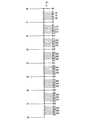
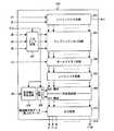
図1は、本実施の形態のDA変換回路100の一構成例を示すブロック図である。 FIG. 1 is a block diagram illustrating a configuration example of the
本実施の形態のDA変換回路100は、0V〜8Vで与えられる参照電圧を64分割し、64通り(64レベル)の階調表示用アナログ電圧(以下、基準電圧と称する)から、5Vの信号で与えられる6ビットのデジタルデータD(5:0)に対応する電圧を出力するものである。DA変換回路100は、図1に示すように、基準電圧発生回路101、選択回路102、バッファ103、およびレベル変換回路104を備えている。 The
基準電圧発生回路101は、外部電源(図示せず)から与えられる参照電圧V0〜V8を64分割して、64階調の基準電圧G(63:0)を発生するものである。基準電圧発生回路101は、作成した基準電圧G(63:0)を選択回路102に出力する。なお、参照電圧V0には8Vが、参照電圧V8には0Vが与えられ、中間電圧の参照電圧V1〜V7にはそれぞれ、7V,6V,5V,4V,3V,2V,1Vが与えられる。 The reference
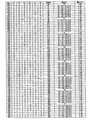
基準電圧発生回路101の具体的な一構成例を図2に示す。図2に示すように、基準電圧発生回路101は、参照電圧V0が入力される端子と参照電圧V1が入力される端子との間、参照電圧V1が入力される端子と参照電圧V2が入力される端子との間、参照電圧V2が入力される端子と参照電圧V3が入力される端子との間、参照電圧V3が入力される端子と参照電圧V4が入力される端子との間、参照電圧V4が入力される端子と参照電圧V5が入力される端子との間、参照電圧V5が入力される端子と参照電圧V6が入力される端子との間、参照電圧V6が入力される端子と参照電圧V7が入力される端子との間、および、参照電圧V7が入力される端子と参照電圧V8が入力される端子との間、が抵抗分割によりそれぞれ等間隔で8分割された構成を有している。これにより、64階調の基準電圧G(63:0)が作成される。64階調の基準電圧G(63:0)における各電圧の算出式および値を図3に示す。 A specific configuration example of the reference
なお、上記基準電圧発生回路101の設定では、64階調の基準電圧G(63:0)として等間隔の電圧が作成されているが、これに限らず、中間電圧である参照電圧V1〜V7の電圧値や、抵抗の比率などの設定を変更することにより、表示のガンマカーブに対応した64階調の基準電圧G(63:0)を作成することができる。また、抵抗の比率の設定のみでガンマカーブに対応可能の場合には、中間電圧である参照電圧V1〜V7を省略して、参照電圧V8および参照電圧V0の2電圧のみにて64階調の基準電圧G(63:0)を作成することができる。 In the setting of the reference
選択回路102は、デジタルデータD(5:0)に基づいて、基準電圧発生回路101で作成された64階調の基準電圧G(63:0)から1つの電圧OUTを選択するものである。なお、デジタルデータD(5:0)は、電圧レベルが変換されたデータDP(5:0)、NDP(4:0)、DN(5:0)、およびNDN(4:0)として、レベル変換回路104から供給される。選択回路102は、選択した電圧OUTをバッファ103に出力する。 The
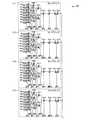
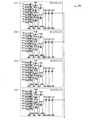
選択回路102の具体的な一構成例を図4および図5に示す。なお、図面のサイズの都合上、選択回路102は、図4および図5に分割して図示している。 A specific configuration example of the
図4および図5に示すように、選択回路102は、V0−1ブロック111、V1−2ブロック112、V2−3ブロック113、V3−4ブロック114、V4−5ブロック115、V5−6ブロック116、V6−7ブロック117、およびV7−8ブロック118が、並列に接続された構成を有している。すなわち、所定の範囲の基準電圧G(63:0)を選択するように各ブロック111〜118が区分されており、各ブロック111〜118の出力が1つにまとめられて、選択回路102の出力端子となっている。 As shown in FIGS. 4 and 5, the
V0−1ブロック111は、参照電圧V0から参照電圧V1の間(8V〜7Vの範囲)で作成される基準電圧G0〜G7を選択するために構成された回路部である。V0−1ブロック111は、PchMOSトランジスタP001〜P018により構成されている。PchMOSトランジスタP001〜P018は、耐圧5Vのロジックトランジスタである。ロジックトランジスタは、主にロジックに使用するものであり、動作速度を速くするために低抵抗化が施されている。また、耐圧5Vのトランジスタとは、5Vの動作電圧で使用するトランジスタの意味であり、絶対最大定格値は5Vよりも大きく、例えば6V程度あるトランジスタである。 The V0-1
V1−2ブロック112は、参照電圧V1から参照電圧V2の間(7V〜6Vの範囲)で作成される基準電圧G8〜G15を選択するために構成された回路部である。V1−2ブロック112は、PchMOSトランジスタP101〜P118により構成されている。PchMOSトランジスタP101〜P118は、耐圧5Vのロジックトランジスタである。 The V1-2
V2−3ブロック113は、参照電圧V2から参照電圧V3の間(6V〜5Vの範囲)で作成される基準電圧G16〜G23を選択するために構成された回路部である。V2−3ブロック113は、PchMOSトランジスタP201〜P218により構成されている。PchMOSトランジスタP201〜P218は、耐圧5Vのロジックトランジスタである。 The V2-3
V3−4ブロック114は、参照電圧V3から参照電圧V4の間(5V〜4Vの範囲)で作成される基準電圧G24〜G31を選択するために構成された回路部である。V3−4ブロック114は、PchMOSトランジスタP301〜P318により構成されている。PchMOSトランジスタP301〜P318は、耐圧5Vのロジックトランジスタである。 The V3-4
V4−5ブロック115は、参照電圧V4から参照電圧V5の間(4V〜3Vの範囲)で作成される基準電圧G32〜G39を選択するために構成された回路部である。V4−5ブロック115は、NchMOSトランジスタN401〜N418により構成されている。NchMOSトランジスタN401〜N418は、耐圧5Vのロジックトランジスタである。 The V4-5
V5−6ブロック116は、参照電圧V5から参照電圧V6の間(3V〜2Vの範囲)で作成される基準電圧G40〜G47を選択するために構成された回路部である。V5−6ブロック116は、NchMOSトランジスタN501〜N518により構成されている。NchMOSトランジスタN501〜N518は、耐圧5Vのロジックトランジスタである。 The V5-6
V6−7ブロック117は、参照電圧V6から参照電圧V7の間(2V〜1Vの範囲)で作成される基準電圧G48〜G55を選択するために構成された回路部である。V6−7ブロック117は、NchMOSトランジスタN601〜N618により構成されている。NchMOSトランジスタN601〜N618は、耐圧5Vのロジックトランジスタである。 The V6-7
V7−8ブロック118は、参照電圧V7から参照電圧V8の間(1V〜0Vの範囲)で作成される基準電圧G56〜G63を選択するために構成された回路部である。V7−8ブロック118は、NchMOSトランジスタN701〜N718により構成されている。NchMOSトランジスタN701〜N718は、耐圧5Vのロジックトランジスタである。 The V7-8
上記各ブロック111〜118では、各MOSトランジスタは、全て、基準電圧発生回路101側にソースが配置されるように構成されている。また、上記各ブロック111〜114に構成されている各PchMOSトランジスタのゲートには、レベル変換回路104から供給されるデータDP(5:0)およびNDP(4:0)が与えられるようになっている。一方、上記各ブロック115〜118に構成されている各NchMOSトランジスタのゲートには、レベル変換回路104から供給されるデータDN(5:0)およびNDN(4:0)が与えられるようになっている。 In each of the
これにより、各データに応じて各MOSトランジスタのオン/オフが切り替えられることで、上記各MOSトランジスタのオン/オフ状態に従って、基準電圧G0〜G63のうち何れか1つの基準電圧が電圧OUTとして出力される。言い換えると、上記各ブロック111〜118では、MOSトランジスタからなるスイッチ群が構成されており、各データに応じてスイッチのオン/オフを行うことにより、基準電圧G0〜G63のうち何れか1つの基準電圧を選択している。 As a result, each MOS transistor is turned on / off according to each data, so that one of the reference voltages G0 to G63 is output as the voltage OUT according to the on / off state of each MOS transistor. Is done. In other words, in each of the
ここで、図6に、上記各ブロック111〜118に用いられているPchMOSトランジスタ121およびNchMOSトランジスタ122の断面構造を示す。 FIG. 6 shows a cross-sectional structure of the
PchMOSトランジスタ121は、V0−1ブロック111、V1−2ブロック112、V2−3ブロック113、並びにV3−4ブロック114に構成されているPchMOSトランジスタP001〜P018、P101〜P118、P201〜P218、並びにP301〜P318を示している。PchMOSトランジスタ121では、N−Wellに参照電圧V0を与えることにより、バックゲート電位が8Vとなっている。 The
V0−1ブロック111、V1−2ブロック112、V2−3ブロック113、並びにV3−4ブロック114の各PchMOSトランジスタのソース・ドレインには、各ブロックに与えられる基準電圧の電圧が掛かる。すなわち、本実施例では8V〜4Vの電圧が掛かる。ソース・ドレイン間は、ソース・ドレインからバックゲート方向に寄生ダイオードが形成されるため、寄生ダイオードに電流が流れないように、バックゲートにはソース・ドレインに掛かる電圧以上の電圧を掛ける必要がある。それゆえ、バックゲート電位を8Vにしている。 A reference voltage applied to each block is applied to the source and drain of each PchMOS transistor in the V0-1
NchMOSトランジスタ122は、V4−5ブロック115、V5−6ブロック116、V6−7ブロック117、並びにV7−8ブロック118に構成されているNchMOSトランジスタN401〜NP418、N501〜N518、N601〜N618、並びにN701〜N718を示している。NchMOSトランジスタ122では、N−Wellの中に形成したP−Wellに参照電圧V8を与えることにより、バックゲート電位が0Vとなっている。 The
バックゲート電位を0Vにするのは、上記PchMOSトランジスタで述べたと同様に、NchMOSトランジスタのソース・ドレインとバックゲート間の寄生ダイオードに電流が流れないようにするためである。 The back gate potential is set to 0 V in order to prevent a current from flowing through the parasitic diode between the source / drain and the back gate of the Nch MOS transistor, as described for the Pch MOS transistor.
なお、基板となるP−基板の電位も0Vであるので、参照電圧V8が0Vの場合は、NchMOSトランジスタ122を図6に示すような構造にする必要は無いが、参照電圧V8をP−基板の電位と異なる値(例えば1Vなど)に設定する場合は必要となる。 Since the potential of the P-substrate serving as the substrate is also 0V, when the reference voltage V8 is 0V, the
バッファ103は、DA変換回路100の出力部に相当し、選択回路102から出力された電圧OUTを後段の構成に出力する。バッファ103の構成は、従来周知の構成を用いればよい。 The
レベル変換回路104は、デジタルデータD(5:0)の電圧レベル(信号レベル)を昇圧などにより変換するものである。本実施例では、5Vの信号で与えられるデジタルデータD(5:0)を、振幅が4V〜8Vの信号となるデータDP(5:0)およびNDP(4:0)と、振幅が0V〜4Vの信号となるデータDN(5:0)およびNDN(4:0)とに変換する。レベル変換回路104は、変換した各データを選択回路102に出力する。 The
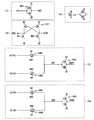
レベル変換回路104の具体的な一構成例を図7に示す。レベル変換回路104は、図7に示す回路部131〜134が組み合わせられた構成を有している。なお、詳細ブロック135は、回路部133・134に示されるアナログスイッチASW1〜ASW4の詳細な構成を示している。 A specific configuration example of the
図7では、0V〜5Vで振幅するD0(デジタルデータD(5:0)の最下位ビット)を、4V〜8Vで振幅するDP0およびNDP0と、0V〜4Vで振幅するDN0およびNDN0とに変換する場合について説明するが、その他のDP1〜5、NDP1〜4、DN1〜5、NDN1〜4においても同様に作成され得る。 In FIG. 7, D0 (the least significant bit of the digital data D (5: 0)) that swings from 0V to 5V is converted into DP0 and NDP0 that swings from 4V to 8V, and DN0 and NDN0 that swings from 0V to 4V. However, other DP1-5, NDP1-4, DN1-5, and NDN1-4 can be similarly created.
レベル変換回路104では、供給されたデジタルデータD(5:0)が、まず、回路部131と回路部132とにそれぞれ入力される。 In the
回路部131では、D0が、0Vと5Vとを電源とするインバータINV1に入力される。インバータINV1は、ソースを0VとするNchMOSトランジスタと、ソースを5VとするPchMOSトランジスタとにより構成されている。インバータINV1は、D0を入力するとD0を反転したND0を出力する。このND0は、回路部132に供給される。 In the
回路部132では、D0およびND0がレベルシフタLEV1に入力され、該レベルシフタLEV1から、0Vから8Vで振幅するD0´およびND0´が出力される。このD0´およびND0´は、回路部133と回路部134とにそれぞれ供給され、アナログスイッチASW1〜ASW4のオン/オフを切り替える制御信号となる。 In the
なお、レベルシフタLEV1にて変換する電圧レベルは0V〜8Vに限るものではなく、基準電圧の電圧範囲を少なくとも含む電圧範囲であればよい(例えば、電源電圧が0〜8Vでも、基準電圧の電圧範囲が0.5V〜7.5Vであれば、電圧範囲は0.5V〜7.5Vでよい。)。 Note that the voltage level converted by the level shifter LEV1 is not limited to 0V to 8V, and may be a voltage range including at least the voltage range of the reference voltage (for example, the voltage range of the reference voltage even when the power supply voltage is 0 to 8V). Is 0.5V to 7.5V, the voltage range may be 0.5V to 7.5V).
回路部133では、アナログスイッチASW1・ASW2、並びにインバータINV2が構成されている。アナログスイッチASW1・ASW2は、詳細ブロック135に示されるPchMOSトランジスタとNchMOSトランジスタとを使用したアナログスイッチである。NchMOSトランジスタのゲートに“H”レベルの信号、かつ、Pchトランジスタのゲートの“L”レベルの信号が入力されたときにオンとなる。 In the
アナログスイッチASW1は、NchMOSトランジスタのゲートにD0´が供給され、PchMOSトランジスタのゲートにND0´が供給される。また、アナログスイッチASW1の一方の端子には、8Vの電圧が与えられている。この8Vの電圧には、基準電圧発生回路101に供給される参照電圧V0、もしくは、基準電圧発生回路101から出力される基準電圧G0が使用される。 In the analog switch ASW1, D0 ′ is supplied to the gate of the NchMOS transistor, and ND0 ′ is supplied to the gate of the PchMOS transistor. A voltage of 8V is applied to one terminal of the analog switch ASW1. The reference voltage V0 supplied to the reference
アナログスイッチASW2は、NchMOSトランジスタのゲートにND0´が供給され、PchMOSトランジスタのゲートにD0´が供給される。また、アナログスイッチASW2の一方の端子には、4Vの電圧が与えられている。この4Vの電圧には、基準電圧発生回路101に供給される参照電圧V4、もしくは、基準電圧発生回路101から出力される基準電圧G32が使用される。 In the analog switch ASW2, ND0 ′ is supplied to the gate of the NchMOS transistor, and D0 ′ is supplied to the gate of the PchMOS transistor. A voltage of 4V is applied to one terminal of the analog switch ASW2. The reference voltage V4 supplied to the reference
また、アナログスイッチASW1の他方の端子と、アナログスイッチASW2の他方の端子とは、インバータINV2に共通に接続されている。これにより、D0´が“H(8V)”のとき、アナログスイッチASW1がオン、アナログスイッチASW2がオフとなり、8VのDP0がインバータINV2に出力される。一方、D0´が“L(0V)”のとき、アナログスイッチASW1がオフ、アナログスイッチASW2がオンとなり、4VのDP0がインバータINV2に出力される。このように、D0´の“H”・“L”と同様にDP0も“H”・“L”が変化するとともに、DP0は4V〜8Vの信号となる。 The other terminal of the analog switch ASW1 and the other terminal of the analog switch ASW2 are commonly connected to the inverter INV2. Thus, when D0 ′ is “H (8V)”, the analog switch ASW1 is turned on, the analog switch ASW2 is turned off, and 8V DP0 is output to the inverter INV2. On the other hand, when D0 ′ is “L (0 V)”, the analog switch ASW1 is turned off, the analog switch ASW2 is turned on, and 4V DP0 is output to the inverter INV2. As described above, DP0 also changes to “H” / “L” as well as “H” / “L” of D0 ′, and DP0 becomes a signal of 4V to 8V.
インバータINV2は、ソースを4VとするNchMOSトランジスタと、ソースを8VとするPchMOSトランジスタとにより構成されている。インバータINV2は、DP0を入力するとDP0を反転したNDP0を出力する。この回路部133にて作成された4V〜8Vで振幅するDP0およびNDP0が、選択回路102に供給される。 The inverter INV2 includes an NchMOS transistor whose source is 4V and a PchMOS transistor whose source is 8V. The inverter INV2 outputs NDP0 obtained by inverting DP0 when DP0 is input. DP0 and NDP0 having an amplitude of 4V to 8V created by the
また、回路部134では、アナログスイッチASW3・ASW4、並びにインバータINV3が構成されている。アナログスイッチASW3・ASW4は、詳細ブロック135に示されるPchMOSトランジスタとNchMOSトランジスタとを使用したアナログスイッチである。 In the
アナログスイッチASW3は、NchMOSトランジスタのゲートにD0´が供給され、PchMOSトランジスタのゲートにND0´が供給される。また、アナログスイッチASW3の一方の端子には、4Vの電圧が与えられている。この4Vの電圧には、基準電圧発生回路101に供給される参照電圧V4、もしくは、基準電圧発生回路101から出力される基準電圧G32が使用される。 In the analog switch ASW3, D0 ′ is supplied to the gate of the NchMOS transistor, and ND0 ′ is supplied to the gate of the PchMOS transistor. A voltage of 4V is applied to one terminal of the analog switch ASW3. The reference voltage V4 supplied to the reference
アナログスイッチASW4は、NchMOSトランジスタのゲートにND0´が供給され、PchMOSトランジスタのゲートにD0´が供給される。また、アナログスイッチASW4の一方の入力には、0Vの電圧が与えられている。この0Vの電圧には、基準電圧発生回路101に供給される参照電圧V8、もしくは、基準電圧発生回路101から出力される基準電圧G63が使用される。 In the analog switch ASW4, ND0 ′ is supplied to the gate of the NchMOS transistor, and D0 ′ is supplied to the gate of the PchMOS transistor. Also, a voltage of 0 V is applied to one input of the analog switch ASW4. The reference voltage V8 supplied to the reference
また、アナログスイッチASW3の他方の端子と、アナログスイッチASW4の他方の端子とは、インバータINV3に共通に接続されている。これにより、D0´が“H(8V)”のとき、アナログスイッチASW3がオン、アナログスイッチASW4がオフとなり、4VのDN0がインバータINV3に出力される。一方、D0´が“L(0V)”のとき、アナログスイッチASW3がオフ、アナログスイッチASW4がオンとなり、0VのDN0がインバータINV3に出力される。このように、D0´の“H”・“L”と同様にDN0も“H”・“L”が変化するとともに、DN0は0V〜4Vの信号となる。 The other terminal of the analog switch ASW3 and the other terminal of the analog switch ASW4 are connected in common to the inverter INV3. Thereby, when D0 ′ is “H (8V)”, the analog switch ASW3 is turned on, the analog switch ASW4 is turned off, and 4V DN0 is output to the inverter INV3. On the other hand, when D0 ′ is “L (0V)”, the analog switch ASW3 is turned off and the analog switch ASW4 is turned on, and 0V DN0 is output to the inverter INV3. In this manner, DN0 changes to “H” and “L” as well as “H” and “L” of D0 ′, and DN0 becomes a signal of 0V to 4V.
インバータINV3は、ソースを0VとするNchMOSトランジスタと、ソースを4VとするPchMOSトランジスタとにより構成されている。インバータINV3は、DN0を入力するとDN0を反転したNDN0を出力する。この回路部134にて作成された0V〜4Vで振幅するDN0およびNDN0が、選択回路102に供給される。 The inverter INV3 is composed of an NchMOS transistor whose source is 0V and a PchMOS transistor whose source is 4V. When the inverter INV3 receives DN0, the inverter INV3 outputs NDN0 obtained by inverting DN0. DN0 and NDN0 generated in the
このようにして、レベル変換回路104は、0V〜5Vで振幅するデジタルデータD(5:0)を、4V〜8Vで振幅するデータDP(5:0)およびNDP(4:0)と、0V〜4Vで振幅するデータDN(5:0)およびNDN(4:0)とに変換している。データ情報は、データDP(5:0)およびDN(5:0)がデジタルデータD(5:0)と同極性であり、データNDP(4:0)およびNDN(4:0)がデジタルデータD(5:0)と逆極性である。 In this way, the
次に、本実施の形態のDA変換回路100の動作について説明する。 Next, the operation of the
まず、外部電源(図示せず)から参照電圧V0〜V8が供給されると、基準電圧発生回路101は、参照電圧V0〜V8に基づいて64階調の基準電圧G(63:0)を作成し、選択回路102に出力する。なお、DA変換回路100の動作を停止する場合を除き、参照電圧V0〜V8は供給され続けているので、基準電圧発生回路101は、常に、64階調の基準電圧G(63:0)を選択回路102に出力している。 First, when reference voltages V0 to V8 are supplied from an external power supply (not shown), the reference
一方、レベル変換回路104では、制御部(図示せず)などから、6ビットのデジタルデータD(5:0)が供給される。このデジタルデータD(5:0)は、図3に示すように、00H〜3FH(16進法表示)の64通りある。 On the other hand, the
レベル変換回路104に、例えば、D(5:0)=00Hのデータが供給されたとする。この場合、D(5:0)=00Hのデータは[000000]となっており、レベル変換回路104は、これに応じた、データDP(5:0)、NDP(4:0)、DN(5:0)、およびNDN(4:0)を作成し、選択回路102に出力する。 For example, it is assumed that data of D (5: 0) = 00H is supplied to the
選択回路102では、レベル変換回路104から供給されたD(5:0)=00Hに従った各データにより、V0−1ブロック111のPchMOSトランジスタP001・P009・P013・P015・P016・P017・P018がオンとなる。これにより、基準電圧G0〜G63のうち基準電圧G0すなわち8Vの電圧が、電圧OUTとしてバッファ103に出力される。つまりは、D(5:0)=00Hのデータに応じた電圧として、8Vの電圧OUTが出力されることになる。 In the
同様の動作により、D(5:0)=00H〜1FHのデジタルデータがレベル変換回路104に供給される場合は、V0−1ブロック111、V1−2ブロック112、V2−3ブロック113、並びにV3−4ブロック114に構成されているPchMOSトランジスタP001〜P018、P101〜P118、P201〜P218、並びにP301〜P318が、レベル変換回路104からのD(5:0)=00H〜1FHの各々に従った各データに応じてオンとなる。これにより、選択回路102からは、基準電圧G0〜G31の何れかが、電圧OUTとしてバッファ103に出力される。 By the same operation, when digital data of D (5: 0) = 00H to 1FH is supplied to the
D(5:0)=00H〜1FHのデジタルデータがレベル変換回路104に供給されている間は、V0−1ブロック111、V1−2ブロック112、V2−3ブロック113、並びにV3−4ブロック114に構成されているPchMOSトランジスタP001〜P018、P101〜P118、P201〜P218、並びにP301〜P318のソースおよびドレインにかかる電圧は、基準電圧G0〜G31、すなわち8V〜4V(正確には4.13Vであるが簡易的に4Vと表現する)である。また、上記PchMOSトランジスタP001〜P018、P101〜P118、P201〜P218、並びにP301〜P318のゲートに与えられる電圧は4V〜8Vである。よって、ゲート・ソース間電圧およびゲート・ドレイン間電圧は常に4V以下であり、PchMOSトランジスタP001〜P018、P101〜P118、P201〜P218、並びにP301〜P318の耐圧(5V)を超えることは無い。 While digital data of D (5: 0) = 00H to 1FH is supplied to the
また、D(5:0)=20H〜3FHのデータがレベル変換回路104に供給される場合は、V4−5ブロック115、V5−6ブロック116、V6−7ブロック117、並びにV7−8ブロック118に構成されているNchMOSトランジスタN401〜N418、N501〜N518、N601〜N618、並びにN701〜N718が、レベル変換回路104からのD(5:0)=20H〜3FHの各々に従った各データに応じてオンとなる。これにより、選択回路102からは、基準電圧G32〜G63の何れかが、電圧OUTとしてバッファ103に出力される。 When data of D (5: 0) = 20H to 3FH is supplied to the
D(5:0)=20H〜3FHのデジタルデータがレベル変換回路104に供給されている間は、V4−5ブロック115、V5−6ブロック116、V6−7ブロック117、並びにV7−8ブロック118構成されているNchMOSトランジスタN401〜N418、N501〜N518、N601〜N618、並びにN701〜N718のソースおよびドレインにかかる電圧は、基準電圧G32〜G63、すなわち4V〜0V(正確には0.13Vであるが簡易的に0Vと表現する)である。また、上記NchMOSトランジスタN401〜N418、N501〜N518、N601〜N618、並びにN701〜N718のゲートに与えられる電圧は0V〜4Vである。よって、ゲート・ソース間電圧、およびゲート・ドレイン間電圧は常に4V以下であり、NchMOSトランジスタN401〜N418、N501〜N518、N601〜N618、並びにN701〜N718の耐圧(5V)を超えることは無い。 While digital data of D (5: 0) = 20H to 3FH is supplied to the
したがって、DA変換回路100では、選択回路102が各ブロック111〜118に区分けされており、レベル変換回路104が、各ブロック111〜118が選択する基準電圧の範囲に応じて電圧レベルを変換したデータDP(5:0)、NDP(4:0)、DN(5:0)、およびNDN(4:0)を上記各ブロック111〜118にそれぞれ供給することによって、上記各MOSトランジスタのソース、ドレイン、およびゲートには、MOSトランジスタの耐圧を超えないように電圧を与えることが可能となっている。 Therefore, in the
これにより、基準電圧G(63:0)の電圧範囲(0V〜8V)がロジックトランジスタの耐圧(5V)より広くても、8Vを満足する耐圧のMOSトランジスタを必ずしも構成する必要が無くなり、ロジックトランジスタにより選択回路102を構成することが可能となる。よって、チップサイズを縮小できるので、DA変換回路100の回路規模を縮小化し、かつコストダウンを行うことが可能となる。 As a result, even if the voltage range (0V to 8V) of the reference voltage G (63: 0) is wider than the breakdown voltage (5V) of the logic transistor, it is not always necessary to configure a MOS transistor having a breakdown voltage satisfying 8V. Thus, the
ここで、上述したDA変換回路100では、選択回路102において、出力端子につながる、例えばPchMOSトランジスタP018には、ゲートを共通とするPchMOSトランジスタP017が接続されている。これは、PchMOSトランジスタP018が1個の場合(ゲートを共通とするPchMOSトランジスタP017が接続されていない場合)、ソース・ドレイン間電圧が耐圧を超える場合が発生するためである。 Here, in the
例えば、D(5:0)=20Hの場合、4Vの電圧OUTが出力される。このとき、V0−1ブロック111では、PchMOSトランジスタP001・P009・P013・P015・P016がオンしているため、PchMOSトランジスタP017・P018の両端の電圧は8Vと4Vになる。 For example, when D (5: 0) = 20H, a voltage OUT of 4V is output. At this time, in the V0-1
このとき、本回路例では参照電圧V0が8Vであるので、PchMOSトランジスタP017,P018の両端の電圧は4Vであり、PchMOSトランジスタP017,P018のように分割する必要は無い。しかしながら、参照電圧V0が例えば16Vになった場合は、D(5:0)=20Hのときの出力は8Vで、PchMOSトランジスタP017,P018の両端の電圧は8Vになる。1個のトランジスタで構成した場合、ソース・ドレイン間電圧が8Vとなるため、耐圧5Vを超えてしまい、動作の保障がなくなる。また、絶対最大定格を超えた場合は破壊に至る可能性もある。本回路では、基準電圧発生回路101の電圧範囲が高くなった場合も考慮して構成されている。 At this time, since the reference voltage V0 is 8V in this circuit example, the voltage across the PchMOS transistors P017 and P018 is 4V, and there is no need to divide like the PchMOS transistors P017 and P018. However, when the reference voltage V0 is 16V, for example, the output when D (5: 0) = 20H is 8V, and the voltage across the Pch MOS transistors P017 and P018 is 8V. In the case of a single transistor, since the source-drain voltage is 8 V, the breakdown voltage exceeds 5 V, and the operation is not guaranteed. If the absolute maximum rating is exceeded, there is a possibility of destruction. This circuit is configured in consideration of the case where the voltage range of the reference
PchMOSトランジスタを2個にした場合、両端からかかる電圧が分圧され、各々のPchMOSトランジスタのソース・ドレイン間電圧が4Vとなり、耐圧以下にすることが可能となる。これにより、選択回路102では、出力端子につながるPchMOSトランジスタP018・P118・P218・P318、並びにNchMOSトランジスタN418・N518・N618・N718には、ゲートを共通とするPchMOSトランジスタおよびNchMOSトランジスタをそれぞれ接続している。 When two PchMOS transistors are used, the voltage is divided from both ends, and the voltage between the source and drain of each PchMOS transistor becomes 4 V, which can be reduced to a withstand voltage or less. As a result, in the
このように分圧を行うことによって、各MOSトランジスタのソース・ドレイン間電圧が耐圧を越えることを防止し、誤動作を回避している。なお、2個のトランジスタを設けても耐圧を超える場合は、トランジスタの数を増やして分割数を増やせばよい。 By performing voltage division in this way, the source-drain voltage of each MOS transistor is prevented from exceeding the withstand voltage, and malfunction is avoided. Note that if the breakdown voltage is exceeded even when two transistors are provided, the number of divisions may be increased by increasing the number of transistors.
〔実施の形態2〕
本発明の他の実施の形態について図面に基づいて説明すれば、以下の通りである。なお、本実施の形態において説明すること以外の構成は、前記実施の形態1と同じである。また、説明の便宜上、前記の実施の形態1の図面に示した部材と同一の機能を有する部材については、同一の符号を付し、その説明を省略する。[Embodiment 2]
The following will describe another embodiment of the present invention with reference to the drawings. Configurations other than those described in the present embodiment are the same as those in the first embodiment. For convenience of explanation, members having the same functions as those shown in the drawings of the first embodiment are given the same reference numerals, and explanation thereof is omitted.
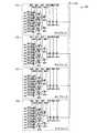
図8は、本実施の形態のDA変換回路200の一構成例を示すブロック図である。 FIG. 8 is a block diagram illustrating a configuration example of the
本実施の形態のDA変換回路200は、0V〜16Vで与えられる参照電圧を64分割し、64通りの基準電圧G(63:0)から、5Vの信号で与えられる6ビットのデジタルデータD(5:0)に対応する電圧を出力するものである。DA変換回路200は、図8に示すように、基準電圧発生回路101、選択回路202、バッファ103、およびレベル変換回路204を備えている。 The
基準電圧発生回路101は、作成した基準電圧G(63:0)を選択回路202に出力する。なお、本実施例では、参照電圧V0には16Vが、参照電圧V8には0Vが与えられ、中間電圧の参照電圧V1〜V7にはそれぞれ、14V,12V,10V,8V,6V,4V,2Vが与えられる。64階調の基準電圧G(63:0)における各電圧の算出式および値を図9に示す。 The reference
選択回路202は、デジタルデータD(5:0)に基づいて、基準電圧発生回路101で作成された64階調の基準電圧G(63:0)から1つの電圧OUTを選択するものである。なお、デジタルデータD(5:0)は、電圧レベルが変換されたデータDA(2:0)、NDA(2:0)、DB(2:0)、NDB(2:0)、DC(2:0)、NDC(2:0)、DD(2:0)、NDD(2:0)、DE(2:0)、NDE(2:0)、DF(2:0),NDF(2:0)、DG(2:0)、NDG(2:0)、DH(2:0)、NDH(2:0)、DU(5:3)、およびNDU(4:3)として、レベル変換回路204から供給される。選択回路202は、選択した電圧OUTをバッファ103に出力する。 The
選択回路202の具体的な一構成例を図10および図11に示す。なお、図面のサイズの都合上、選択回路202は、図10および図11に分割して図示している。 A specific configuration example of the
図10および図11に示すように、選択回路202は、V0−1ブロック211、V1−2ブロック212、V2−3ブロック213、V3−4ブロック214、V4−5ブロック215、V5−6ブロック216、V6−7ブロック217、およびV7−8ブロック218が、並列に接続された構成を有している。すなわち、所定の範囲の基準電圧G(63:0)を選択するように各ブロック211〜218が区分されており、各ブロック211〜218の出力が1つにまとめられて、選択回路202の出力端子となっている。 As shown in FIGS. 10 and 11, the
V0−1ブロック211は、参照電圧V0から参照電圧V1の間(16V〜14Vの範囲)で作成される基準電圧G0〜G7を選択するために構成された回路部である。V0−1ブロック211は、耐圧3VのロジックトランジスタであるPchMOSトランジスタP021〜P034と、耐圧が16V以上の中耐圧トランジスタであるPchMOSトランジスタP035〜P037とにより構成されている。PchMOSトランジスタP021〜P034のゲートには、レベル変換回路104から供給されるデータDA(2:0)およびNDA(2:0)が与えられる。PchMOSトランジスタP035〜P037のゲートには、レベル変換回路104から供給されるデータDU(5:3)およびNDU(4:3)が与えられる。 The V0-1
V1−2ブロック212は、参照電圧V1から参照電圧V2の間(14V〜12Vの範囲)で作成される基準電圧G8〜G15を選択するために構成された回路部である。V1−2ブロック212は、耐圧3VのロジックトランジスタであるPchMOSトランジスタP121〜P134と、耐圧が16V以上の中耐圧トランジスタであるPchMOSトランジスタP135〜P137とにより構成されている。PchMOSトランジスタP121〜P134のゲートには、レベル変換回路104から供給されるデータDB(2:0)およびNDB(2:0)が与えられる。PchMOSトランジスタP135〜P137のゲートには、レベル変換回路104から供給されるデータDU(5:3)およびNDU(4:3)が与えられる。 The V1-2
V2−3ブロック213は、参照電圧V2から参照電圧V3の間(12V〜10Vの範囲)で作成される基準電圧G16〜G23を選択するために構成された回路部である。V2−3ブロック213は、耐圧3VのロジックトランジスタであるPchMOSトランジスタP221〜P234と、耐圧が16V以上の中耐圧トランジスタであるPchMOSトランジスタP235〜P237とにより構成されている。PchMOSトランジスタP221〜P234のゲートには、レベル変換回路104から供給されるデータDC(2:0)およびNDC(2:0)が与えられる。PchMOSトランジスタP235〜P237のゲートには、レベル変換回路104から供給されるデータDU(5:3)およびNDU(4:3)が与えられる。 The V2-3
V3−4ブロック214は、参照電圧V3から参照電圧V4の間(10V〜8Vの範囲)で作成される基準電圧G24〜G31を選択するために構成された回路部である。V3−4ブロック214は、耐圧3VのロジックトランジスタであるPchMOSトランジスタP321〜P334と、耐圧が16V以上の中耐圧トランジスタであるPchMOSトランジスタP335〜P337とにより構成されている。PchMOSトランジスタP321〜P334のゲートには、レベル変換回路104から供給されるデータDD(2:0)およびNDD(2:0)が与えられる。PchMOSトランジスタP335〜P337のゲートには、レベル変換回路104から供給されるデータDU(5:3)およびNDU(4:3)が与えられる。 The V3-4
V4−5ブロック215は、参照電圧V4から参照電圧V5の間(8V〜6Vの範囲)で作成される基準電圧G32〜G39を選択するために構成された回路部である。V4−5ブロック215は、耐圧3VのロジックトランジスタであるNchMOSトランジスタN421〜N434と、耐圧が16V以上の中耐圧トランジスタであるNchMOSトランジスタN435〜N437とにより構成されている。NchMOSトランジスタN421〜N434のゲートには、レベル変換回路104から供給されるデータDE(2:0)およびNDE(2:0)が与えられる。NchMOSトランジスタN435〜N437のゲートには、レベル変換回路104から供給されるデータDU(5:3)およびNDU(4:3)が与えられる。 The V4-5
V5−6ブロック216は、参照電圧V5から参照電圧V6の間(6V〜4Vの範囲)で作成される基準電圧G40〜G47を選択するために構成された回路部である。V5−6ブロック216は、耐圧3VのロジックトランジスタであるNchMOSトランジスタN521〜N534と、耐圧が16V以上の中耐圧トランジスタであるNchMOSトランジスタN535〜N537とにより構成されている。NchMOSトランジスタN521〜N534のゲートには、レベル変換回路104から供給されるデータDF(2:0)およびNDF(2:0)が与えられる。NchMOSトランジスタN535〜N537のゲートには、レベル変換回路104から供給されるデータDU(5:3)およびNDU(4:3)が与えられる。 The V5-6
V6−7ブロック217は、参照電圧V6から参照電圧V7の間(4V〜2Vの範囲)で作成される基準電圧G48〜G55を選択するために構成された回路部である。V6−7ブロック217は、耐圧3VのロジックトランジスタであるNchMOSトランジスタN621〜N634と、耐圧が16V以上の中耐圧トランジスタであるNchMOSトランジスタN635〜N637とにより構成されている。NchMOSトランジスタN621〜N634のゲートには、レベル変換回路104から供給されるデータDG(2:0)およびNDG(2:0)が与えられる。NchMOSトランジスタN635〜N637のゲートには、レベル変換回路104から供給されるデータDU(5:3)およびNDU(4:3)が与えられる。 The V6-7
V7−8ブロック218は、参照電圧V7から参照電圧V8の間(2V〜0Vの範囲)で作成される基準電圧G56〜G63を選択するために構成された回路部である。V7−8ブロック218は、耐圧3VのロジックトランジスタであるNchMOSトランジスタN721〜N734と、耐圧が16V以上の中耐圧トランジスタであるNchMOSトランジスタN735〜N737とにより構成されている。NchMOSトランジスタN721〜N734のゲートには、レベル変換回路104から供給されるデータDH(2:0)およびNDH(2:0)が与えられる。NchMOSトランジスタN735〜N737のゲートには、レベル変換回路104から供給されるデータDU(5:3)およびNDU(4:3)が与えられる。 The V7-8
上記各ブロック211〜218では、各MOSトランジスタは、全て、基準電圧発生回路101側にソースが配置されるように構成されている。 In each of the
これにより、デジタルデータに応じて各MOSトランジスタのオン/オフが切り替えられることで、上記各MOSトランジスタのオン/オフ状態に従って、基準電圧G0〜G63のうち何れか1つの基準電圧が電圧OUTとして出力される。言い換えると、上記各ブロック211〜218では、MOSトランジスタからなるスイッチ群が構成されており、各データに応じてスイッチのオン/オフを行うことにより、基準電圧G0〜G63のうち何れか1つの基準電圧を選択している。 As a result, each MOS transistor is turned on / off according to the digital data, so that one of the reference voltages G0 to G63 is output as the voltage OUT according to the on / off state of each MOS transistor. Is done. In other words, in each of the
ここで、図12に、上記各ブロック211〜218に用いられている耐圧3VのPchMOSトランジスタ221〜224、並びにNchMOSトランジスタ225〜228の断面構造を示す。 Here, FIG. 12 shows a cross-sectional structure of the
PchMOSトランジスタ221は、V0−1ブロック211に構成されているPchMOSトランジスタP021〜P034を示している。PchMOSトランジスタ221では、N−Wellに参照電圧V0を与えることにより、バックゲート電位が16Vとなっている。
PchMOSトランジスタ222は、V1−2ブロック212に構成されているPchMOSトランジスタP121〜P134を示している。PchMOSトランジスタ222では、N−Wellに参照電圧V1を与えることにより、バックゲート電位が14Vとなっている。
なお、バックゲート電位に、前記実施の形態1のように参照電圧V0を使用して16Vを与えても、寄生ダイオードに電流は流れないため問題はない。しかしながら、V1−2ブロック212には参照電圧V0が直接与えられていないため、該ブロックに与えられる参照電圧の中で一番電圧の高い参照電圧V1を使用することが、配置において有利である。以下の他のブロックも同様である。 It should be noted that there is no problem even if 16 V is applied to the back gate potential using the reference voltage V0 as in the first embodiment, since no current flows through the parasitic diode. However, since the reference voltage V0 is not directly applied to the V1-2
PchMOSトランジスタ223は、V2−3ブロック213に構成されているPchMOSトランジスタP221〜P234を示している。PchMOSトランジスタ223では、N−Wellに参照電圧V2を与えることにより、バックゲート電位が12Vとなっている。
PchMOSトランジスタ224は、V3−4ブロック214に構成されているPchMOSトランジスタP321〜P334を示している。PchMOSトランジスタ224では、N−Wellに参照電圧V3を与えることにより、バックゲート電位が10Vとなっている。
NchMOSトランジスタ225は、V4−5ブロック215に構成されているNchMOSトランジスタN421〜N434を示している。NchMOSトランジスタ225では、N−Wellの中に形成したP−Wellに参照電圧V5を与えることにより、バックゲート電位が6Vとなっている。
NchMOSトランジスタ226は、V5−6ブロック216に構成されているNchMOSトランジスタN521〜N534を示している。NchMOSトランジスタ226では、N−Wellの中に形成したP−Wellに参照電圧V6を与えることにより、バックゲート電位が4Vとなっている。
NchMOSトランジスタ227は、V6−7ブロック217に構成されているNchMOSトランジスタN621〜N634を示している。NchMOSトランジスタ227では、N−Wellの中に形成したP−Wellに参照電圧V7を与えることにより、バックゲート電位が2Vとなっている。
NchMOSトランジスタ228は、V7−8ブロック218に構成されているNchMOSトランジスタN721〜N734を示している。NchMOSトランジスタ228では、N−Wellの中に形成したP−Wellに参照電圧V8を与えることにより、バックゲート電位が0Vとなっている。
また、図13に、上記各ブロック211〜218に用いられている耐圧16V以上のPchMOSトランジスタ231およびNchMOSトランジスタ232の断面構造を示す。 FIG. 13 shows a cross-sectional structure of a
PchMOSトランジスタ231は、V0−1ブロック211、V1−2ブロック212、V2−3ブロック213、並びにV3−4ブロック214に構成されているPchMOSトランジスタP035〜P037、P135〜P137、P235〜P237、並びにP335〜P337を示している。PchMOSトランジスタ231では、N−WellにVH(VHは、参照電圧V0以上の電圧、例えば16V)を与えることにより、バックゲートがVHとなっている。 The
NchMOSトランジスタ232は、V4−5ブロック215、V5−6ブロック216、V6−7ブロック217、並びにV7−8ブロック218に構成されているNchMOSトランジスタN435〜N437、N535〜N537、N635〜N637、並びにN735〜N737を示している。NchMOSトランジスタ232では、バックゲートが基板電位VL(VLは、通常0VのGND電位である)となっている。 The
レベル変換回路204は、デジタルデータD(5:0)の電圧レベルを昇圧などにより変換するものである。本実施例では、3Vの信号で与えられるデジタルデータD(5:0)を、
振幅が14V〜16Vの信号となるデータDA(2:0)およびNDA(2:0)と、
振幅が12V〜14Vの信号となるデータDB(2:0)およびNDB(2:0)と、
振幅が10V〜12Vの信号となるデータDC(2:0)およびNDC(2:0)と、
振幅が8V〜10Vの信号となるデータDD(2:0)およびNDD(2:0)と、
振幅が6V〜8Vの信号となるデータDE(2:0)およびNDE(2:0)と、
振幅が4V〜6Vの信号となるデータDF(2:0)およびNDF(2:0)と、
振幅が2V〜4Vの信号となるデータDG(2:0)およびNDG(2:0)と、
振幅が0V〜2Vの信号となるデータDH(2:0)およびNDH(2:0)と、
振幅が0V〜16Vの信号となるデータDU(5:3)およびNDU(4:3)と、
に変換する。レベル変換回路104は、変換した各データを選択回路202に出力する。The
Data DA (2: 0) and NDA (2: 0), which are signals having an amplitude of 14V to 16V,
Data DB (2: 0) and NDB (2: 0), which are signals having an amplitude of 12V to 14V,
Data DC (2: 0) and NDC (2: 0), which are signals having an amplitude of 10V to 12V,
Data DD (2: 0) and NDD (2: 0), which are signals having an amplitude of 8V to 10V,
Data DE (2: 0) and NDE (2: 0) which are signals having an amplitude of 6V to 8V,
Data DF (2: 0) and NDF (2: 0), which are signals having an amplitude of 4V to 6V,
Data DG (2: 0) and NDG (2: 0), which are signals having an amplitude of 2V to 4V,
Data DH (2: 0) and NDH (2: 0), which are signals having an amplitude of 0V to 2V,
Data DU (5: 3) and NDU (4: 3) that are signals having an amplitude of 0V to 16V,
Convert to The
なお、レベル変換回路204は、図7に示したようなレベル変換回路104を構成する回路部131〜134を、供給電圧を適宜変更しながら組み合わせることにより構成することができ、レベル変換回路204の変換動作は、上述したレベル変換回路204の変換動作と基本的に同じである。 The
データ情報は、データDA(2:0)、DB(2:0)、DC(2:0)、DD(2:0)、DE(2:0)、DF(2:0)、DG(2:0)、DF(2:0)、およびDU(5:3)が、デジタルデータD(5:0)と同極性である。また、データNDA(2:0)、NDB(2:0)、NDC(2:0)、NDD(2:0)、NDE(2:0)、NDF(2:0)、NDG(2:0)、NDF(2:0)、およびNDU(4:3)が、デジタルデータD(5:0)と逆極性である。 Data information includes data DA (2: 0), DB (2: 0), DC (2: 0), DD (2: 0), DE (2: 0), DF (2: 0), DG (2 : 0), DF (2: 0), and DU (5: 3) have the same polarity as the digital data D (5: 0). Also, data NDA (2: 0), NDB (2: 0), NDC (2: 0), NDD (2: 0), NDE (2: 0), NDF (2: 0), NDG (2: 0) ), NDF (2: 0), and NDU (4: 3) are opposite in polarity to the digital data D (5: 0).
上記構成を有するDA変換回路200は、前記実施の形態1で述べたDA変換回路100の動作と同様に動作する。DA変換回路200の注目すべき点は、選択回路202において、デジタルデータD(5:0)の下位3ビットに対応するデータが供給される部分の回路が、耐圧3Vのロジックトランジスタで構成することが可能な点である。 The
つまりは、V0−1ブロック211では、基準電圧G0〜G7、すなわち16V〜14.25Vの電圧が入力される。また、V0−1ブロック211に供給される下位3ビットデータDA(2:0)およびNDA(2:0)は、14V〜16Vの信号である。さらには、PchMOSトランジスタP021〜P034のバックゲートの電圧は16Vとなっている。よって、ゲート・ソース間電圧、およびゲート・ドレイン間電圧は、常に2V以下であり、PchMOSトランジスタP021〜P034の耐圧(3V)を超えることは無い。 That is, in the V0-1
V1−2ブロック212では、基準電圧G8〜G15、すなわち14V〜12.25Vの電圧が入力される。また、V1−2ブロック212に供給される下位3ビットデータDB(2:0)およびNDB(2:0)は、12V〜14Vの信号である。さらには、PchMOSトランジスタP121〜P134のバックゲートの電圧は14Vとなっている。よって、ゲート・ソース間電圧、およびゲート・ドレイン間電圧は、常に2V以下であり、PchMOSトランジスタP121〜P134の耐圧(3V)を超えることは無い。 In the V1-2
V2−3ブロック213では、基準電圧G16〜G23、すなわち12V〜10.25Vの電圧が入力される。また、V2−3ブロック213に供給される下位3ビットデータDC(2:0)およびNDC(2:0)は、10V〜12Vの信号である。さらには、PchMOSトランジスタP221〜P234のバックゲートの電圧は12Vとなっている。よって、ゲート・ソース間電圧、およびゲート・ドレイン間電圧は、常に2V以下であり、PchMOSトランジスタP221〜P234の耐圧(3V)を超えることは無い。 In the V2-3
V3−4ブロック214では、基準電圧G24〜G31、すなわち10V〜8.25Vの電圧が入力される。また、V3−4ブロック214に供給される下位3ビットデータDD(2:0)およびNDD(2:0)は、8V〜10Vの信号である。さらには、PchMOSトランジスタP321〜P334のバックゲートの電圧は10Vとなっている。よって、ゲート・ソース間電圧、およびゲート・ドレイン間電圧は、常に2V以下であり、PchMOSトランジスタP321〜P334の耐圧(3V)を超えることは無い。 In the V3-4
V4−5ブロック215では、基準電圧G32〜G39、すなわち8V〜6.25Vの電圧が入力される。また、V4−5ブロック215に供給される下位3ビットデータDE(2:0)およびNDE(2:0)は、6V〜8Vの信号である。さらには、NchMOSトランジスタN421〜N434のバックゲートの電圧は6Vとなっている。よって、ゲート・ソース間電圧、およびゲート・ドレイン間電圧は、常に2V以下であり、NchMOSトランジスタN421〜N434の耐圧(3V)を超えることは無い。 In the V4-5
V5−6ブロック216では、基準電圧G40〜G47、すなわち6V〜4.25Vの電圧が入力される。また、V5−6ブロック216に供給される下位3ビットデータDF(2:0)およびNDF(2:0)は、4V〜6Vの信号である。さらには、NchMOSトランジスタN521〜N534のバックゲートの電圧は4Vとなっている。よって、ゲート・ソース間電圧、およびゲート・ドレイン間電圧は、常に2V以下であり、NchMOSトランジスタN521〜N534の耐圧(3V)を超えることは無い。 In the V5-6
V6−7ブロック217では、基準電圧G48〜G55、すなわち4V〜2.25Vの電圧が入力される。また、V6−7ブロック217に供給される下位3ビットデータDG(2:0)およびNDG(2:0)は、2V〜4Vの信号である。さらには、NchMOSトランジスタN621〜N634のバックゲートの電圧は2Vとなっている。よって、ゲート・ソース間電圧、およびゲート・ドレイン間電圧は、常に2V以下であり、NchMOSトランジスタN621〜N634の耐圧(3V)を超えることは無い。 In the V6-7
V7−8ブロック218では、基準電圧G56〜G63、すなわち2V〜0.25Vの電圧が入力される。また、V7−8ブロック218に供給される下位3ビットデータDH(2:0)およびNDH(2:0)は、0V〜2Vの信号である。さらには、NchMOSトランジスタN721〜N734のバックゲートの電圧は0Vとなっている。よって、ゲート・ソース間電圧、およびゲート・ドレイン間電圧は、常に2V以下であり、NchMOSトランジスタN721〜N734の耐圧(3V)を超えることは無い。 In the V7-8
したがって、DA変換回路200では、選択回路202が各ブロック211〜218に区分けされており、レベル変換回路204が、各ブロック211〜218が選択する基準電圧の範囲に応じて電圧レベルを変換したデータDA(2:0)、NDA(2:0)、DB(2:0)、NDB(2:0)、DC(2:0)、NDC(2:0)、DD(2:0)、NDD(2:0)、DE(2:0)、NDE(2:0)、DF(2:0),NDF(2:0)、DG(2:0)、NDG(2:0)、DH(2:0)、およびNDH(2:0)を上記各ブロック211〜218にそれぞれ供給することによって、上記各データが与えられる各MOSトランジスタのソース、ドレイン、およびゲートには、MOSトランジスタの耐圧を超えないように電圧を与えることが可能となっている。 Therefore, in the
これにより、DA変換回路200では、基準電圧G(63:0)の電圧範囲(0V〜16V)がロジックトランジスタの耐圧(3V)より広くても、16Vを満足する耐圧のMOSトランジスタを必ずしも構成する必要が無くなり、データ下位3ビットが選択する部分の回路はロジックトランジスタを用いて選択回路202を構成することが可能となる。よって、チップサイズを縮小できるので、DA変換回路200の回路規模を縮小化し、かつコストダウンを行うことが可能となる。 Thereby, in the
但し、DA変換回路200では、デジタルデータD(5:0)の上位3ビットに対応するデータDU(5:3)およびNDU(4:3)が供給される部分の回路は、16V以上の耐圧のある中耐圧トランジスタで構成している。 However, in the
例えば、D(5:0)=00Hの場合、16Vの電圧OUTが出力される。このとき、V2−3ブロック213では、PchMOSトランジスタP221・P229・P233・P235・P237がオンするため、オフ状態のPchMOSトランジスタP236のソース・ドレインには基準電圧G16の電位と電圧OUTの電位とが与えられることになる。基準電圧G16は12Vであり、電圧OUTは16Vであるので、ソース・ドレイン間電圧は4Vとなり、耐圧3Vを超えてしまう。 For example, when D (5: 0) = 00H, a voltage OUT of 16V is output. At this time, in the V2-3
またこのとき、V4−5ブロック215では、NchMOSトランジスタN421・N429・N433・N435・N436がオンするため、オフ状態のNchMOSトランジスタN437の両端には基準電圧G32の電位と電圧OUTの電位とが与えられることになる。基準電圧G32は8Vであり、電圧OUTは16Vであるので、ソース・ドレイン間電圧は8Vとなり、耐圧3Vを超えてしまう。 At this time, in the V4-5
このように、データ上位3ビットで選択される回路の各MOSトランジスタは、ロジックトランジスタの耐圧を超える電圧がかかる場合がある。このため、選択回路202では、データ上位3ビットが選択する部分の回路は16V以上の耐圧のある中耐圧トランジスタで構成している。中耐圧トランジスタはロジックトランジスタと比べトランジスタサイズを大きくする必要があり、チップサイズが大きくなるが、選択回路202では、スイッチ群を構成する大半のMOSトランジスタをロジックトランジスタを用いて構成しているので、トータルとして回路規模を縮小することが可能となっている。 Thus, each MOS transistor of the circuit selected by the upper 3 bits of data may be applied with a voltage exceeding the breakdown voltage of the logic transistor. For this reason, in the
つまりは、選択回路202では、出力端子に現れる電圧によっては、出力端子側に位置するMOSトランジスタのソース・ドレイン間電圧が耐圧を越えてしまう場合が発生するが、少なくとも各基準電圧が1番目に入力される各MOSトランジスタのソース、ドレイン、およびゲートには、MOSトランジスタの耐圧を超えないように電圧を与えることが可能であるので、ロジックトランジスタを用いて回路を縮小化することが可能となっている。 That is, in the
〔実施の形態3〕
本発明の他の実施の形態について図面に基づいて説明すれば、以下の通りである。なお、本実施の形態において説明すること以外の構成は、前記実施の形態1,2と同じである。また、説明の便宜上、前記の実施の形態1,2の図面に示した部材と同一の機能を有する部材については、同一の符号を付し、その説明を省略する。[Embodiment 3]
The following will describe another embodiment of the present invention with reference to the drawings. Configurations other than those described in the present embodiment are the same as those in the first and second embodiments. For convenience of explanation, members having the same functions as those shown in the drawings of the first and second embodiments are given the same reference numerals, and explanation thereof is omitted.
本実施例では、前記実施の形態1のDA変換回路100を、図18に示したようなソースドライバ900に使用する場合について説明する。なお、DA変換回路100に限らず、前記実施の形態2のDA変換回路200を使用してもよいし、他の一般的なソースドライバに適用することもできる。 In this example, a case where the
図14は、本実施の形態のソースドライバに構成されるDA変換回路100aの一構成例を示すブロック図である。なお、図1に示すようにDA変換回路100はバッファ103を構成していたが、バッファ103はソースドライバの出力回路907に対応するので、図14ではバッファ103は記載していない。 FIG. 14 is a block diagram illustrating a configuration example of the
本実施の形態のソースドライバ(表示用駆動装置)は、図18に示した入力ラッチ回路901、シフトレジスタ回路902、サンプリングメモリ回路903、ホールドメモリ回路904(取得手段)、および出力回路907(出力手段)と、図14に示すDA変換回路100a(DA変換手段)および反転回路301(反転手段)とを備えている。 The source driver (display driving device) of this embodiment includes an
本実施の形態のソースドライバでは、液晶パネルのソースラインを交流化駆動するために、図17に示した共通電極交流駆動が行われる。共通電極交流駆動は、例えば、コントローラ(図示せず)から出力される交流化を行うタイミングを示す信号(交流化信号REV)に基づいて行う。 In the source driver of the present embodiment, the common electrode AC driving shown in FIG. 17 is performed in order to drive the source line of the liquid crystal panel to AC. The common electrode AC drive is performed based on, for example, a signal (AC signal REV) indicating the timing of AC conversion output from a controller (not shown).
DA変換回路100aは、図14に示すように、基準電圧発生回路101A・101B、選択回路102、レベル変換回路104、アナログスイッチASW10〜ASW18、アナログスイッチASW20〜ASW28、並びに、アナログスイッチASW30・ASW31を備えている。 As shown in FIG. 14, the
基準電圧発生回路101A・101Bは、基準電圧発生回路101と同一の構成および機能を有するものである。但し、基準電圧発生回路101Aには、アナログスイッチASW10〜ASW18がそれぞれ設けられている各経路から、参照電圧V0〜V8が供給されている。アナログスイッチASW10〜ASW18は、NchMOSトランジスタのゲートに信号UREVが供給され、PchMOSトランジスタのゲートに信号NUREVが供給されている。 The reference
また、基準電圧発生回路101Bには、アナログスイッチASW20〜ASW28が設けられている各経路から、参照電圧V0〜V8が供給されている。アナログスイッチASW20〜ASW28は、NchMOSトランジスタのゲートに信号NUREVが供給され、PchMOSトランジスタのゲートに信号UREVが供給されている。 Further, reference voltages V0 to V8 are supplied to the reference
つまりは、アナログスイッチASW10〜ASW18、並びにアナログスイッチASW20〜ASW28のオン/オフにより、基準電圧発生回路101Aおよび基準電圧発生回路101Bのいずれか一方に、参照電圧V0〜V8が供給される。なお、信号UREVは0V〜5Vの振幅のREV信号を0V〜8Vへレベルシフトした信号であり、信号NUREVは信号UREVの反転信号である。また、アナログスイッチASW10〜ASW18、並びにアナログスイッチASW20〜ASW28の設置は、使用しない基準電圧発生回路に電流が流れることを防ぐという目的もある。 That is, the reference voltages V0 to V8 are supplied to either the reference
基準電圧発生回路101Aの出力は、アナログスイッチASW30を介して、アナログスイッチASW31を介した基準電圧発生回路101Bの出力に接続されるとともに、選択回路102に接続されている。アナログスイッチASW30は、NchMOSトランジスタのゲートに交流化信号REVが供給され、PchMOSトランジスタのゲートに信号NREVが供給されている。アナログスイッチASW31は、NchMOSトランジスタのゲートに信号NREVが供給され、PchMOSトランジスタのゲートに交流化信号REVが供給されている。 The output of the reference
つまりは、アナログスイッチASW30・ASW31のオン/オフにより、基準電圧発生回路101Aにより作成された基準電圧GP(63:0)、および基準電圧発生回路101Bにより作成された基準電圧GN(63:0)のいずれか一方が、基準電圧G(63:0)として、選択回路102に出力される。 That is, the reference voltage GP (63: 0) created by the reference
反転回路301は、選択回路102の出力の極性を所定の周期で反転させる手段である。詳細には、反転回路301は、レベル変換回路104の前段に設けられ、レベル変換回路104に与えるデジタル表示データD(5:0)を、所定の周期で極性を反転させながら転送する。所定の周期は、交流化を行う周期であり、交流化信号REVにより制御される。また、デジタル表示データD(5:0)は、ホールドメモリ回路904から供給される。これにより、デジタル表示データD(5:0)は、反転回路301により処理されたデジタル表示データDR(5:0)として、レベル変換回路104に供給される。 The inversion circuit 301 is means for inverting the polarity of the output of the
反転回路301の具体的な一構成例を図15に示す。反転回路301は、図15に示す回路部311・312により構成されている。図15では、0V〜5Vで振幅するD0(デジタル表示データD(5:0)の最下位ビット)を反転する場合について説明するが、その他のD1〜D5においても同様に反転され得る。 A specific configuration example of the inverting circuit 301 is shown in FIG. The inverting circuit 301 includes
反転回路301では、デジタル表示データD(5:0)および交流化信号REVが与えられると、デジタル表示データD(5:0)は回路部312に入力され、交流化信号REVは回路部311・312に入力される。 In the inverting circuit 301, when the digital display data D (5: 0) and the alternating signal REV are given, the digital display data D (5: 0) is input to the
回路部311では、インバータ313により、交流化信号REVを反転した信号NREVが作成される。この信号NREVは、回路部312に供給されるとともに、アナログスイッチASW30・ASW31にも供給される。 In the
回路部312では、インバータ314・315並びにアナログスイッチASW32を直列に接続した回路と、インバータ316およびアナログスイッチASW33を直列に接続した回路とが並列に接続されている。アナログスイッチASW32・ASW33は、図7に示した詳細ブロック135に示されるPchMOSトランジスタとNchMOSトランジスタとを使用したアナログスイッチである。 In the
アナログスイッチASW32は、NchMOSトランジスタのゲートに交流化信号REVが供給され、PchMOSトランジスタのゲートに信号NREVが供給されている。アナログスイッチASW33は、NchMOSトランジスタのゲートに信号NREVが供給され、PchMOSトランジスタのゲートに交流化信号REVが供給されている。 In the analog switch ASW32, the AC signal REV is supplied to the gate of the NchMOS transistor, and the signal NREV is supplied to the gate of the PchMOS transistor. In the analog switch ASW33, the signal NREV is supplied to the gate of the NchMOS transistor, and the AC signal REV is supplied to the gate of the PchMOS transistor.
交流化信号REVが“H”のとき、アナログスイッチASW32がオン、アナログスイッチASW33がオフとなり、D0はインバータを2段接続してDR0につながる。一方、交流化信号REVが“L”のとき、アナログスイッチASW32がオフ、アナログスイッチASW33がオンとなり、D0はインバータ1段でDR0につながる。それゆえ、交流化信号REVが“H”のときD0とDR0との極性は同一となり、交流化信号REVが“L”のときD0とDR0との極性が反転することになる。 When the AC signal REV is “H”, the analog switch ASW32 is turned on, the analog switch ASW33 is turned off, and D0 is connected to DR0 by connecting two stages of inverters. On the other hand, when the AC signal REV is “L”, the analog switch ASW32 is turned off and the analog switch ASW33 is turned on, and D0 is connected to DR0 in one stage of the inverter. Therefore, the polarity of D0 and DR0 is the same when the alternating signal REV is “H”, and the polarity of D0 and DR0 is inverted when the alternating signal REV is “L”.
次に、本実施の形態のソースドライバにおけるDA変換回路100aの動作について説明する。なお、DA変換回路100aは、反転回路301を用いた共通電極交流駆動のための制御が追加される点を除いて、前記実施の形態1で述べたDA変換回路100の動作と同様に動作する。 Next, the operation of the
共通電極交流駆動は、コントローラ(図示せず)から出力される交流化信号REVが、図17の交流化信号Mの波形に示されるように、“H”と“L”とで交互に切り替わることにより制御されている。以下では、交流化信号REVが“H”の場合と、交流化信号REVが“L”の場合とに分けて説明する。 In the common electrode AC drive, the AC signal REV output from the controller (not shown) is alternately switched between “H” and “L” as shown in the waveform of the AC signal M in FIG. It is controlled by. In the following, the case where the alternating signal REV is “H” and the case where the alternating signal REV is “L” will be described separately.
“H”の交流化信号REVが出力された場合、このとき、信号UREVは“H”であるので、アナログスイッチASW10〜ASW18はオンとなり、アナログスイッチASW20〜ASW28はオフとなる。これにより、参照電圧V0〜V8は基準電圧発生回路101Aに供給される。またこのとき、アナログスイッチASW30はオンとなり、アナログスイッチASW31はオフとなるので、基準電圧発生回路101Aで作成された基準電圧GP(63:0)が、基準電圧G(63:0)として選択回路102に与えられる。 When the “H” AC signal REV is output, at this time, since the signal UREV is “H”, the analog switches ASW10 to ASW18 are turned on, and the analog switches ASW20 to ASW28 are turned off. Thereby, the reference voltages V0 to V8 are supplied to the reference
一方、反転回路301では、交流化信号REVが“H”であるので、デジタル表示データD(5:0)と同極性のデジタル表示データDR(5:0)が、レベル変換回路104に出力される。そして、レベル変換回路104にて作成されたデータDP(5:0)、NDP(4:0)、DN(5:0)、およびNDN(4:0)に基づいて、選択回路102において基準電圧G(63:0)から1つ(電圧OUT)が選択され、次段の出力回路907に出力される。 On the other hand, in the inverting circuit 301, since the alternating signal REV is “H”, the digital display data DR (5: 0) having the same polarity as the digital display data D (5: 0) is output to the
図16は、交流化信号REVが“H”の場合と “L”の場合とにおける、64階調の基準電圧G(63:0)の値を示す表である。 FIG. 16 is a table showing the value of the reference voltage G (63: 0) of 64 gradations when the AC signal REV is “H” and “L”.
このように、交流化信号REVが“H”である場合は反転回路301で極性反転は起こらないので、選択回路102から出力される電圧OUTは、前記実施の形態1で述べたDA変換回路100と同様に、D(5:0)=00Hであれば基準電圧G0を選択し、8Vの電圧OUTが出力される。 In this way, when the AC signal REV is “H”, polarity inversion does not occur in the inverting circuit 301, so the voltage OUT output from the
“L”の交流化信号REVが出力された場合、このとき、信号UREVは“L”であるので、アナログスイッチASW10〜ASW18はオフとなり、アナログスイッチASW20〜ASW28はオンとなる。これにより、参照電圧V0〜V8は基準電圧発生回路101Bに供給される。またこのとき、アナログスイッチASW30はオフとなり、アナログスイッチASW31はオンとなるので、基準電圧発生回路101Bで作成された基準電圧GN(63:0)が、基準電圧G(63:0)として選択回路102に与えられる。 When the “L” AC signal REV is output, since the signal UREV is “L” at this time, the analog switches ASW10 to ASW18 are turned off and the analog switches ASW20 to ASW28 are turned on. Thereby, the reference voltages V0 to V8 are supplied to the reference
一方、反転回路301では、交流化信号REVが“L”であるので、デジタル表示データD(5:0)の極性を反転したデジタル表示データDR(5:0)が、レベル変換回路104に出力される。そして、レベル変換回路104にて作成されたデータDP(5:0)、NDP(4:0)、DN(5:0)、およびNDN(4:0)に基づいて、選択回路102において基準電圧G(63:0)から1つ(電圧OUT)が選択され、次段の出力回路907に出力される。 On the other hand, in the inversion circuit 301, since the AC signal REV is “L”, the digital display data DR (5: 0) obtained by inverting the polarity of the digital display data D (5: 0) is output to the
このように、交流化信号REVが“L”である場合は反転回路301で極性反転が起こるので、選択回路102から出力される電圧OUTは、D(5:0)=00Hであれば基準電圧G63を選択し、0.13Vの電圧OUTが出力される。 Thus, when the AC signal REV is “L”, polarity inversion occurs in the inverting circuit 301. Therefore, the voltage OUT output from the
よって、交流化信号REVが“H”と“L”とのときでデジタル表示データD(5:0)を反転させることにより、選択回路102から出力される電圧OUTの極性を反転させることが可能となる。それゆえ、ソースドライバは、容易に共通電極交流駆動を行うことが可能である。 Therefore, the polarity of the voltage OUT output from the
また、共通電極交流化駆動を使用して表示を行う表示パネル(液晶パネル)において、ソース電極の信号レベルが集積回路のロジックトランジスタで構成できない電圧を必要とする場合であっても、本実施の形態のDA変換回路100aを備えるソースドライバであれば、選択回路102をロジックトランジスタで構成することが可能となっているので、ソースドライバのチップサイズを縮小でき、表示パネルのコストを削減することが可能となる。 Further, in a display panel (liquid crystal panel) that performs display using common electrode AC driving, even when the signal level of the source electrode requires a voltage that cannot be configured by the logic transistor of the integrated circuit, the present embodiment In the case of the source driver including the
なお、図2に示したように、基準電圧発生回路101は抵抗により等分割された構成を有しているが、駆動電圧を供給する表示パネルの表示特性に合わせて、階調電圧を設定するγ調整を抵抗分割の抵抗比により行うことがある。上述したDA変換回路100aでは、基準電圧発生回路を2個使用しているので、極性反転でのγの変更が可能となっている。 As shown in FIG. 2, the reference
また、共通電極交流駆動を行うとき、正極性でのγと負極性でのγとが異なる場合が多い。このとき、2個ある基準電圧発生回路101A・101Bを別のγに対応させておくことにより、共通電極交流駆動に好適に対応することができる。 When common electrode AC driving is performed, γ for positive polarity and γ for negative polarity are often different. At this time, by making the two reference
本発明は上述した各実施形態に限定されるものではなく、請求項に示した範囲で種々の変更が可能であり、異なる実施形態にそれぞれ開示された技術的手段を適宜組み合わせて得られる実施形態についても本発明の技術的範囲に含まれる。 The present invention is not limited to the above-described embodiments, and various modifications are possible within the scope shown in the claims, and embodiments obtained by appropriately combining technical means disclosed in different embodiments. Is also included in the technical scope of the present invention.
本発明は、デジタルデータに応じたアナログ電圧を出力するDA変換回路に関する分野に好適に用いることができるだけでなく、DA変換回路の製造方法に関する分野にも好適に用いることができ、さらには、DA変換回路を備える電子機器、例えば、ソースドライバなどの表示用駆動装置や、表示用駆動装置を備えるアクティブマトリクス型の液晶表示装置などの分野にも広く用いることができる。 The present invention can be suitably used not only in a field related to a DA converter circuit that outputs an analog voltage corresponding to digital data, but also in a field related to a method of manufacturing a DA converter circuit. The present invention can also be widely used in the field of electronic equipment including a conversion circuit, for example, a display driving device such as a source driver and an active matrix liquid crystal display device including a display driving device.
100,100a,200 DA変換回路
101,101A,101B 基準電圧発生回路
102,202 選択回路
103 バッファ
104,204 レベル変換回路
132 回路部(レベルシフタ回路)
133,134 回路部(レベル変換データ作成回路)
301 反転回路(反転手段)
901 入力ラッチ回路
902 シフトレジスタ回路
903 サンプリングメモリ回路
904 ホールドメモリ回路(取得手段)
907 出力回路(出力手段)100, 100a, 200
133, 134 circuit part (level conversion data creation circuit)
301 Inversion circuit (inversion means)
901
907 output circuit (output means)
Claims (7)
Translated fromJapanese上記複数の基準電圧に対して所定の範囲の基準電圧を選択するように区分されて構成されている複数のMOSトランジスタを、該各区分にそれぞれ供給されるデジタルデータに基づいて制御することにより、上記複数の基準電圧の中から1つの基準電圧を選択する選択回路と、
上記選択回路の各区分が選択する基準電圧の範囲に応じて電圧レベルを変換したデジタルデータを、該各区分にそれぞれ供給するレベル変換回路とを備え、
上記選択回路の複数のMOSトランジスタは、少なくとも上記各基準電圧が1番目に入力されるMOSトランジスタが、上記第1電圧と上記第2電圧との間の電圧範囲よりも低い耐圧のMOSトランジスタであることを特徴とするDA変換回路。A reference voltage generating circuit that generates a plurality of reference voltages each having a different voltage value between a first voltage and a second voltage greater than the first voltage, using a supplied reference voltage;
By controlling a plurality of MOS transistors divided and configured to select a reference voltage within a predetermined range with respect to the plurality of reference voltages, based on digital data respectively supplied to the respective sections, A selection circuit for selecting one reference voltage from the plurality of reference voltages;
A level conversion circuit for supplying digital data obtained by converting a voltage level according to a range of a reference voltage selected by each section of the selection circuit to each of the sections;
The plurality of MOS transistors of the selection circuit is a MOS transistor whose breakdown voltage is lower than a voltage range between the first voltage and the second voltage, at least the MOS transistor to which each of the reference voltages is input first A DA conversion circuit characterized by that.
上記MOSトランジスタがPchMOSトランジスタの場合、構成されている区分が選択する基準電圧のうち最も電圧値が高い基準電圧の電圧であり、
上記MOSトランジスタがNchMOSトランジスタの場合、構成されている区分が選択する基準電圧のうち最も電圧値が低い基準電圧の電圧であることを特徴とする請求項2に記載のDA変換回路。The voltage applied to the back gate is
When the MOS transistor is a PchMOS transistor, it is the voltage of the reference voltage having the highest voltage value among the reference voltages selected by the configured section,
3. The DA converter circuit according to claim 2, wherein when the MOS transistor is an Nch MOS transistor, a voltage of a reference voltage having the lowest voltage value among reference voltages selected by a configured section is provided.
供給されるデジタルデータを、上記第1電圧以下の電圧と上記第2電圧以上の電圧との間の電圧範囲を有する電圧レベルに変換するレベルシフタ回路と、
上記レベルシフタ回路で変換されたデジタルデータに応じて、第3電圧または上記第3電圧よりも大きい第4電圧を選択することにより、上記第3電圧と上記第4電圧との間の電圧範囲を有する電圧レベルのデジタルデータを作成するレベル変換データ作成回路とを備え、
上記第3電圧および上記第4電圧は、上記選択回路の各区分にそれぞれ供給するデジタルデータの電圧レベルに応じて設定されるとともに、上記基準電圧発生回路に供給される参照電圧、または、上記基準電圧発生回路から発生される基準電圧が使用されることを特徴とする請求項1に記載のDA変換回路。The level conversion circuit is
A level shifter circuit for converting supplied digital data into a voltage level having a voltage range between a voltage equal to or lower than the first voltage and a voltage equal to or higher than the second voltage;
A voltage range between the third voltage and the fourth voltage is selected by selecting a third voltage or a fourth voltage higher than the third voltage according to the digital data converted by the level shifter circuit. A level conversion data creation circuit for creating voltage level digital data,
The third voltage and the fourth voltage are set according to the voltage level of the digital data supplied to each section of the selection circuit, and the reference voltage supplied to the reference voltage generation circuit or the reference voltage 2. The DA converter circuit according to claim 1, wherein a reference voltage generated from the voltage generator circuit is used.
上記表示用デジタルデータに基づいて表示用電圧を出力するDA変換手段と、
上記DA変換手段が出力した表示用電圧を、アクティブマトリクス方式の表示パネルのデータ信号線に印加する出力手段と、
上記DA変換手段が出力する表示用電圧の極性を所定の周期で反転させる反転手段とを備えている表示用駆動装置において、
上記DA変換手段は、請求項1〜6のいずれか1項に記載のDA変換回路であることを特徴とする表示用駆動装置。An acquisition means for capturing digital data for display;
DA conversion means for outputting a display voltage based on the display digital data;
Output means for applying the display voltage output from the DA conversion means to the data signal lines of the active matrix display panel;
In a display driving device comprising: inversion means for inverting the polarity of the display voltage output from the DA conversion means at a predetermined cycle;
The display driving device according to claim 1, wherein the DA conversion unit is the DA conversion circuit according to claim 1.
Priority Applications (1)
| Application Number | Priority Date | Filing Date | Title |
|---|---|---|---|
| JP2008136921AJP2009284426A (en) | 2008-05-26 | 2008-05-26 | Da converting circuit and driving device for display |
Applications Claiming Priority (1)
| Application Number | Priority Date | Filing Date | Title |
|---|---|---|---|
| JP2008136921AJP2009284426A (en) | 2008-05-26 | 2008-05-26 | Da converting circuit and driving device for display |
Publications (1)
| Publication Number | Publication Date |
|---|---|
| JP2009284426Atrue JP2009284426A (en) | 2009-12-03 |
Family
ID=41454366
Family Applications (1)
| Application Number | Title | Priority Date | Filing Date |
|---|---|---|---|
| JP2008136921APendingJP2009284426A (en) | 2008-05-26 | 2008-05-26 | Da converting circuit and driving device for display |
Country Status (1)
| Country | Link |
|---|---|
| JP (1) | JP2009284426A (en) |
Cited By (2)
| Publication number | Priority date | Publication date | Assignee | Title |
|---|---|---|---|---|
| JP2018054394A (en)* | 2016-09-28 | 2018-04-05 | ラピスセミコンダクタ株式会社 | Detection circuit |
| CN111833792A (en)* | 2019-04-15 | 2020-10-27 | 矽创电子股份有限公司 | Level converter |
- 2008
- 2008-05-26JPJP2008136921Apatent/JP2009284426A/enactivePending
Cited By (3)
| Publication number | Priority date | Publication date | Assignee | Title |
|---|---|---|---|---|
| JP2018054394A (en)* | 2016-09-28 | 2018-04-05 | ラピスセミコンダクタ株式会社 | Detection circuit |
| CN111833792A (en)* | 2019-04-15 | 2020-10-27 | 矽创电子股份有限公司 | Level converter |
| CN111833792B (en)* | 2019-04-15 | 2023-08-08 | 矽创电子股份有限公司 | Level converter |
Similar Documents
| Publication | Publication Date | Title |
|---|---|---|
| JP3926651B2 (en) | Display drive device and display device using the same | |
| JP4108360B2 (en) | Display drive device and display device using the same | |
| JP4847702B2 (en) | Display device drive circuit | |
| JP3779166B2 (en) | Gradation display voltage generator and gradation display device having the same | |
| KR100293962B1 (en) | Liquid crystal driving circuit for driving a liquid crystal display panel | |
| JP3795361B2 (en) | Display driving device and liquid crystal display device using the same | |
| US7535451B2 (en) | Liquid crystal drive method, liquid crystal display system, and liquid crystal drive control device in which one specified bit is changed at a switch between a positive phase and a negative phase | |
| WO2010140556A1 (en) | Level shifter circuit, scanning line driver and display device | |
| JP2005266738A (en) | Source driver and liquid crystal display | |
| JP2009186911A (en) | Source driver | |
| CN1877686B (en) | Gradation display reference voltage generating circuit and liquid crystal driving device | |
| TWI415083B (en) | A semiconductor integrated circuit and a semiconductor integrated circuit for driving a liquid crystal display | |
| US12198654B2 (en) | Output amplifier, source driver, and display apparatus | |
| KR101045904B1 (en) | Flat Panel Display Devices and Integrated Circuits | |
| JP3920860B2 (en) | Signal line drive circuit for image display device | |
| JP2009284426A (en) | Da converting circuit and driving device for display | |
| JP5721444B2 (en) | Source driver and liquid crystal display device using the same | |
| KR101232162B1 (en) | Driving circuit for data and method for driving the same | |
| JPH06301356A (en) | Driving circuit for liquid crystal display device | |
| JP2001034241A (en) | Liquid crystal driving device and liquid crystal display device provided with the driving device | |
| WO2005015534A1 (en) | Delay time correction circuit, video data processing circuit, and flat display apparatus | |
| WO2023182278A1 (en) | Da converting device, display driver, and display device | |
| JP2025132141A (en) | Source driver and display device | |
| JP2010204296A (en) | Data driver circuit and display device using the same | |
| KR20120053858A (en) | Organic light emitting diode display device and method of driving the same |