JP2009279408A - System and method of reducing artifact for radiation imaging system - Google Patents
System and method of reducing artifact for radiation imaging systemDownload PDFInfo
- Publication number
- JP2009279408A JP2009279408AJP2009120506AJP2009120506AJP2009279408AJP 2009279408 AJP2009279408 AJP 2009279408AJP 2009120506 AJP2009120506 AJP 2009120506AJP 2009120506 AJP2009120506 AJP 2009120506AJP 2009279408 AJP2009279408 AJP 2009279408A
- Authority
- JP
- Japan
- Prior art keywords
- data
- emi
- image
- image data
- electromagnetic interference
- Prior art date
- Legal status (The legal status is an assumption and is not a legal conclusion. Google has not performed a legal analysis and makes no representation as to the accuracy of the status listed.)
- Pending
Links
- 238000000034methodMethods0.000titleclaimsdescription42
- 230000005855radiationEffects0.000titledescription15
- 238000003384imaging methodMethods0.000titledescription13
- 238000012512characterization methodMethods0.000claimsabstractdescription20
- 238000012545processingMethods0.000claimsdescription18
- 238000012935AveragingMethods0.000claimsdescription5
- 230000001360synchronised effectEffects0.000claims1
- 238000013459approachMethods0.000description15
- 238000012937correctionMethods0.000description14
- 230000000694effectsEffects0.000description9
- 230000008569processEffects0.000description9
- 239000013598vectorSubstances0.000description7
- 239000011159matrix materialSubstances0.000description5
- 238000012805post-processingMethods0.000description5
- 238000010586diagramMethods0.000description4
- 239000010409thin filmSubstances0.000description4
- 238000007476Maximum LikelihoodMethods0.000description3
- 239000000654additiveSubstances0.000description3
- 230000000996additive effectEffects0.000description3
- 238000004891communicationMethods0.000description3
- 239000004020conductorSubstances0.000description3
- 238000001514detection methodMethods0.000description3
- 239000010408filmSubstances0.000description3
- 230000006870functionEffects0.000description3
- 238000007689inspectionMethods0.000description3
- 238000005259measurementMethods0.000description3
- BNPSSFBOAGDEEL-UHFFFAOYSA-Nalbuterol sulfateChemical compoundOS(O)(=O)=O.CC(C)(C)NCC(O)C1=CC=C(O)C(CO)=C1.CC(C)(C)NCC(O)C1=CC=C(O)C(CO)=C1BNPSSFBOAGDEEL-UHFFFAOYSA-N0.000description2
- 238000002591computed tomographyMethods0.000description2
- 238000003745diagnosisMethods0.000description2
- 230000005669field effectEffects0.000description2
- 238000001914filtrationMethods0.000description2
- 230000004807localizationEffects0.000description2
- 238000012986modificationMethods0.000description2
- 230000004048modificationEffects0.000description2
- 238000010521absorption reactionMethods0.000description1
- 230000009471actionEffects0.000description1
- 229910021417amorphous siliconInorganic materials0.000description1
- 238000004458analytical methodMethods0.000description1
- 230000002238attenuated effectEffects0.000description1
- 230000008859changeEffects0.000description1
- 238000013480data collectionMethods0.000description1
- 230000001419dependent effectEffects0.000description1
- 238000013461designMethods0.000description1
- 238000012774diagnostic algorithmMethods0.000description1
- 201000010099diseaseDiseases0.000description1
- 208000037265diseases, disorders, signs and symptomsDiseases0.000description1
- 230000008030eliminationEffects0.000description1
- 238000003379elimination reactionMethods0.000description1
- 238000005516engineering processMethods0.000description1
- 238000007687exposure techniqueMethods0.000description1
- 210000000744eyelidAnatomy0.000description1
- 238000002594fluoroscopyMethods0.000description1
- 238000003702image correctionMethods0.000description1
- 238000003780insertionMethods0.000description1
- 230000037431insertionEffects0.000description1
- 230000007246mechanismEffects0.000description1
- 238000012544monitoring processMethods0.000description1
- 239000013307optical fiberSubstances0.000description1
- 238000005192partitionMethods0.000description1
- 230000010363phase shiftEffects0.000description1
- 238000002601radiographyMethods0.000description1
- 230000009467reductionEffects0.000description1
- 238000005070samplingMethods0.000description1
- 238000005201scrubbingMethods0.000description1
- 230000011218segmentationEffects0.000description1
- 230000035945sensitivityEffects0.000description1
- 238000005309stochastic processMethods0.000description1
- 230000002123temporal effectEffects0.000description1
- 238000012360testing methodMethods0.000description1
- 238000012546transferMethods0.000description1
- 230000000007visual effectEffects0.000description1
Images


Classifications
- H—ELECTRICITY
- H04—ELECTRIC COMMUNICATION TECHNIQUE
- H04N—PICTORIAL COMMUNICATION, e.g. TELEVISION
- H04N23/00—Cameras or camera modules comprising electronic image sensors; Control thereof
- H04N23/30—Cameras or camera modules comprising electronic image sensors; Control thereof for generating image signals from X-rays
- H—ELECTRICITY
- H04—ELECTRIC COMMUNICATION TECHNIQUE
- H04N—PICTORIAL COMMUNICATION, e.g. TELEVISION
- H04N25/00—Circuitry of solid-state image sensors [SSIS]; Control thereof
- H04N25/60—Noise processing, e.g. detecting, correcting, reducing or removing noise
- H04N25/617—Noise processing, e.g. detecting, correcting, reducing or removing noise for reducing electromagnetic interference, e.g. clocking noise
Landscapes
- Engineering & Computer Science (AREA)
- Multimedia (AREA)
- Signal Processing (AREA)
- Physics & Mathematics (AREA)
- Electromagnetism (AREA)
- Apparatus For Radiation Diagnosis (AREA)
- Measurement Of Radiation (AREA)
- Image Processing (AREA)
Abstract
Translated fromJapaneseDescription
Translated fromJapanese本発明は、ディジタルX線イメージング・システムに関し、具体的には、かかるシステムによって取得される画像データにおいて電磁干渉(EMI)の影響を補正する手法に関する。 The present invention relates to digital x-ray imaging systems, and in particular to techniques for correcting the effects of electromagnetic interference (EMI) in image data acquired by such systems.
様々な設計の多数の放射線イメージング・システムが公知であり、現に利用されている。かかるシステムは一般的には、着目した被検体に向けて照射されるX線の発生に基づく。X線は被検体を横断してフィルム又はディジタル検出器に入射する。かかるX線システムが、被検体の介在構造による減弱、散乱又は吸収を受けたX線を検出するためにディジタル・サーキットリを用いる場合が次第に多くなっている。例えば医療診断の状況では、かかるシステムを用いて体内組織を視覚化して患者の病気を診断することができる。他の状況では、部品、手荷物、小荷物及び他の被検体を画像化して、内容物を検査したり他の目的に供したりすることができる。 Numerous radiation imaging systems of various designs are known and are currently in use. Such systems are generally based on the generation of X-rays that are directed towards the subject of interest. X-rays enter the film or digital detector across the subject. Increasingly, such X-ray systems use digital circuitry to detect X-rays that have been attenuated, scattered or absorbed by the intervening structure of the subject. For example, in the context of medical diagnosis, such a system can be used to visualize body tissue to diagnose a patient's disease. In other situations, parts, baggage, parcels and other objects can be imaged to inspect the contents or serve other purposes.
基本的なX線システムは、専ら投影画像を形成するように設計され得る。かかる投影画像は周知の反転画像として提示されてもよいが、画像データ自体は様々な提示法を施される。投影型X線システムに加えて、当技術分野は現在、同様のX線放射線発生及び検出に基づくフルオロスコピィ・システム、計算機式断層写真法システム、及びトモシンセシス・システムを提供している。例えば計算機式断層写真法システム及びトモシンセシス・システムでは、画像は多数の収集画像に適用される様々な再構成手法に基づいて被検体のスライスとして算出される。 A basic X-ray system can be designed exclusively to produce a projected image. Such a projection image may be presented as a known inverted image, but the image data itself is subjected to various presentation methods. In addition to projection x-ray systems, the art currently provides fluoroscopy systems, computed tomography systems, and tomosynthesis systems based on similar x-ray radiation generation and detection. For example, in computed tomography systems and tomosynthesis systems, images are calculated as slices of the subject based on various reconstruction techniques applied to multiple acquired images.
上述の形式のシステムの任意のものにおいて収集される放射線システム・データには、様々なアーティファクトが存在し得る。幾つかの形式のアーティファクトは周知であり、様々な公知の方法において扱われ、解消され又は補正され得る。しかしながら、少なくとも公知の手法では容易に補正又は回避され得ないアーティファクトが依然として存在する。例えば、ディジタル検出器を備えたX線システムは、電磁干渉(EMI)の存在によるアーティファクトを蒙る。EMIの原因としては例えば、幾つかのみ挙げると無線周波数アブレータ及び磁気型カテーテル・ナビゲーション・システム等のようにX線イメージング・システムの近くで用いられ得る様々な電気部品及び電子部品等がある。かかるEMIの位相、周波数及び振幅に依存して、再構成画像のアーティファクトは一般的には、基本画像に重ね合わせられた明暗のある平行な横縞の形態を取り得る。かかるアーティファクトは紛らわしいばかりでなく、医療の状況での診断の場合等に画像の実用性を損なう場合がある。具体的には、かかるアーティファクトは、画像において可視であった筈の微小な又はさらに詳細な特徴の検出及び識別を困難にする場合がある。かかるアーティファクトはまた、医療診断の状況、並びに部品及び手荷物検査の状況において益々普及しつつあるコンピュータ支援式検出及び診断アルゴリズム、並びにセグメント分割アルゴリズム等のようなコンピュータ支援式手法の実用性を妨げる場合がある。 There can be various artifacts in radiation system data collected in any of the above types of systems. Some types of artifacts are well known and can be handled, resolved or corrected in various known ways. However, there are still artifacts that cannot be easily corrected or avoided by at least known techniques. For example, x-ray systems with digital detectors are subject to artifacts due to the presence of electromagnetic interference (EMI). Causes of EMI include, for example, various electrical and electronic components that can be used near X-ray imaging systems, such as radio frequency ablator and magnetic catheter navigation system, to name just a few. Depending on the phase, frequency and amplitude of such EMI, artifacts in the reconstructed image can generally take the form of bright and dark parallel horizontal stripes superimposed on the base image. Such artifacts are not only confusing, but may impair the practicality of images, such as in the case of diagnosis in a medical situation. In particular, such artifacts may make it difficult to detect and identify minor or more detailed features of the eyelid that were visible in the image. Such artifacts may also interfere with the practicality of computer-aided techniques such as computer-aided detection and diagnostic algorithms, segmentation algorithms, and the like that are becoming increasingly popular in the context of medical diagnostics and parts and baggage inspection is there.
従って、放射線画像データのアーティファクト及び雑音の解消に対する改良型アプローチが必要とされている。また、X線画像におけるEMI起源の雑音に対処し得る手法が特に必要とされている。 Therefore, there is a need for an improved approach to the elimination of radiographic image data artifacts and noise. There is also a particular need for a technique that can deal with EMI-derived noise in X-ray images.
本発明は、かかる必要性に応えるべく設計されたシステム及び方法を提供する。本発明の第一の観点によれば、X線画像データを処理するコンピュータ利用型方法が、X線画像データ及び電磁干渉によって生ずるデータを含む第一のデータを、ディジタル検出器を介して取得するステップを含んでいる。また、電磁干渉によって生ずるデータを含むがX線画像データは含まない第二のデータを、ディジタル検出器を介して取得する。電磁干渉が少なくとも第二のデータに基づいて推定される。第一のデータが、特性決定された電磁干渉に基づいて補正される。 The present invention provides systems and methods designed to meet such needs. According to a first aspect of the present invention, a computer-based method for processing X-ray image data acquires first data including X-ray image data and data generated by electromagnetic interference via a digital detector. Includes steps. Further, second data including data generated by electromagnetic interference but not including X-ray image data is acquired via a digital detector. Electromagnetic interference is estimated based on at least the second data. The first data is corrected based on the characterized electromagnetic interference.
本発明のもう一つの観点によれば、X線画像データを処理するコンピュータ利用型方法が、ディジタル検出器にX線放射線を曝射するステップと、検出器の横列をイネーブルにするステップと、X線画像データ及び電磁干渉によって生ずるデータを含む第一のデータを検出器から読み出すステップと、検出器の横列をディスエーブルにするステップと、電磁干渉によって生ずるデータを含むがX線画像データは含まない第二のデータを検出器から取得するステップとを含んでいる。電磁干渉が少なくとも第二のデータに基づいて推定され、第一のデータが、特性決定された電磁干渉に基づいて補正される。 According to another aspect of the present invention, a computer-based method for processing X-ray image data includes exposing a digital detector to X-ray radiation, enabling a detector row, Reading the first data from the detector, including line image data and data resulting from electromagnetic interference, disabling the detector rows, including data resulting from electromagnetic interference but not X-ray image data Obtaining second data from the detector. Electromagnetic interference is estimated based on at least the second data, and the first data is corrected based on the characterized electromagnetic interference.
本発明のもう一つの観点によれば、X線画像データを処理するコンピュータ利用型方法が、ディジタル検出器を介して取得される第一及び第二のデータであって、X線画像データ及び電磁干渉によって生ずるデータを含む第一のデータと、電磁干渉によって生ずるデータを含むがX線画像データは含まない第二のデータとに基づいて電磁干渉を推定するステップと、特性決定された電磁干渉に基づいて第一のデータを補正するステップとを含んでいる。 According to another aspect of the present invention, a computer-based method for processing X-ray image data includes first and second data acquired via a digital detector, wherein the X-ray image data and electromagnetic Estimating electromagnetic interference based on first data including data caused by interference and second data including data caused by electromagnetic interference but not X-ray image data; and Correcting the first data based on the first data.
本発明はまた、以上に述べた形式の機能を具現化するように設計されたシステムを提供する。 The present invention also provides a system designed to embody functions of the type described above.
本発明のこれらの特徴、観点及び利点、並びに他の特徴、観点及び利点は、添付図面を参照して以下の詳細な説明を精読することにより、さらに十分に理解されよう。尚、図面全体にわたり、類似の参照符号は類似の部材を表わす。
図1は、離散的なピクセル画像データを取得して処理するイメージング・システム10を線図で示している。図示の実施形態では、システム10は、本発明の手法に従って原画像データを取得すること及び画像データを表示用に処理することの両方を行なうように設計されているディジタルX線システムである。図1に示す実施形態では、イメージング・システム10は、コリメータ14に隣接して配置されているX線放射線の線源12を含んでいる。コリメータ14は、患者18のような被検体が配置されている領域に放射線流16を通過させる。放射線の一部20は被検体を透過し又は被検体の周りを通過して、参照番号22に全体的に示すディジタルX線検出器に入射する。後に詳述するように、検出器22は表面で受光したX線フォトンをより低エネルギのフォトンへ変換し、続いて電気信号へ変換し、これらの電気信号が取得され処理されて、被検体の体内の特徴の画像を再構成する。 FIG. 1 shows diagrammatically an
線源12は、検査系列のための電力信号及び制御信号の両方を供給する電源/制御回路24によって制御される。さらに、検出器22は、検出器において発生される信号の取得を指令する検出器制御器26に結合されている。検出器制御器26はまた、ダイナミック・レンジの初期調節及びディジタル画像データのインタリーブ等のような様々な信号処理作用及びフィルタ処理作用を実行することができる。電源/制御回路24及び検出器制御器26の両方がシステム制御器28からの信号に応答する。一般的には、システム制御器28は、イメージング・システムの動作を指令して、検査プロトコルを実行すると共に取得した画像データを処理する。本例では、システム制御器28はまた、汎用ディジタル・コンピュータ又は特定応用向けディジタル・コンピュータを典型的に基本構成要素とした信号処理サーキットリと、コンピュータによって実行されるプログラム及びルーチン、並びに構成パラメータ及び画像データを記憶する付設のメモリ・サーキットリと、インタフェイス回路等とを含んでいる。 The
図1に示す実施形態では、システム制御器28は参照番号30に示す表示器又はプリンタのような少なくとも1台の出力装置に結合されている。出力装置は標準的な又は特殊目的のコンピュータ・モニタ及び付設の処理サーキットリを含んでいてよい。システム・パラメータを出力し、検査を依頼し、画像を視覚化する等のために、システムに1台又は複数の操作者ワークステーション32がさらに結合されていてもよい。一般的には、表示器、プリンタ、ワークステーション、及びシステムの内部に供給されている同様の装置は、データ取得構成要素に対してローカルに位置していてもよいし、これらの構成要素から遠隔に位置していてもよく、施設若しくは病院内の他の場所に位置していてもよいし、全く異なる場所等に位置して、インターネット及び仮想私設網等のような1又は複数の構成自在型網を介して画像取得システムに結合されていてもよい。 In the embodiment shown in FIG. 1, the
本発明の手法によれば、システム10によって取得されるデータは、システムが用いられている状況、及びシステムの周囲に位置し得る装置又はシステムと共に用いられ得る装置に依存して、EMI(図示されていない)の様々な原因による摂動を受ける場合がある。EMIは様々な周波数及び振幅での干渉であって、取得されるデータと位相が揃っている場合もあれば揃っていない場合もあり、取得データが収集されるときに取得データに重ね合わされて影響を及ぼし得る。システムは、かかる干渉の特性決定及び補正を可能にし、従って他の場合であれば画像データに存在してデータに基づく再構成画像において可視となったであろうアーティファクトの低減を可能にする。特性決定及び補正自体は、検出器サーキットリ、検出器制御器又はシステム制御器を含め上述のサーキットリのいずれにおいて実行されてもよい。また、所望がある場合には、干渉は、イメージング・システム自体から部分的に又は完全に遠隔に位置し得る後処理ステップにおいて特性決定され補正されてもよい。 In accordance with the techniques of the present invention, the data acquired by the
図2は、ディジタル検出器22の機能構成要素の線図である。図2はまた、典型的には検出器制御器26の内部で構成される撮像検出器制御器すなわちIDC34を示している。IDC34は、CPU又はディジタル信号プロセッサと、検出器からの検知信号の取得を指令するメモリ回路とを含んでいる。IDC34は、双方向光ファイバ導体を介して検出器22内の検出器制御サーキットリ36に結合されている。現状で思量される幾つかの実施形態では、イーサネット通信プロトコル(「イーサネット」は商標)並びに無線通信装置及びプロトコルのような他の通信システム及び技術を用いてもよい。これにより、IDC34は動作時に検出器内で画像データに関する命令信号を授受する。 FIG. 2 is a diagram of the functional components of the
検出器制御サーキットリ36は、参照番号38に全体的に示す電源からDC電力を受ける。検出器制御サーキットリ36は、システムのデータ取得動作段階時に画像データを取得するのに用いられる横列(row)電子回路及び縦列(column)電子回路のためのタイミング指令及び制御指令を発するように構成されている。従って、サーキットリ36は、参照/調節器サーキットリ40へ電力信号及び制御信号を送信すると共に、サーキットリ40からディジタル画像ピクセル・データを受信する。 The
本実施形態では、検出器22は、検査時に検出器表面で受光したX線フォトンをより低エネルギの(光)フォトンへ変換するシンチレータから成っている。次いで、光検出器のアレイが光フォトンを電気信号へ変換して、これらの電気信号が検出器表面の個々のピクセル領域に入射したフォトンの数又は放射線の強度を表わす。現状で思量される実施形態では、X線フォトンは電気信号へ直接変換され得る。読み出し電子回路は、得られたアナログ信号をディジタル値へ変換し、これらのディジタル値を処理し、記憶させ、また画像の再構成の後に表示器30又はワークステーション32等に表示することができる。本形態では、光検出器のアレイはアモルファス・シリコンで形成されている。アレイ素子は横列及び縦列を成して構成されており、各々の素子がフォトダイオードと薄膜トランジスタとから成っている。各々のダイオードのカソードはトランジスタのソースに接続され、全てのダイオードのアノードが負のバイアス電圧に接続されている。各々の横列のトランジスタのゲートは共に接続されており、横列電極は後述する走査用電子回路に接続されている。縦列1列のトランジスタのドレインは共に接続されており、各々の縦列の電極は読み出し電子回路の個々のチャネルに接続されている。 In the present embodiment, the
図2に示す特定的な実施形態では、例として述べると、横列バス42が、検出器の様々な縦列からの読み出しをイネーブルにすると共に、所望に応じて横列をディスエーブルにし、また選択された横列に電荷補償電圧を印加する複数の導体を含んでいる。また、縦列バス44が、横列が相次いでイネーブルにされている間に縦列からの読み出しを指令する追加の導体を含んでいる。横列バス42は一連の横列ドライバ46に結合されており、横列ドライバ46の各々が、検出器の一連の横列のイネーブルを指令する。同様に、読み出し電子回路48が縦列バス44に結合されており、検出器の全ての縦列の読み出しを指令する。 In the particular embodiment shown in FIG. 2, by way of example,
図示の実施形態では、横列ドライバ46及び読み出し電子回路48は検出器パネル50に結合されており、パネル50は複数の区画52に分割されていてよい。各々の区画52が横列ドライバ46の一つ一つに結合されており、また一定数の横列を含んでいる。同様に、各々の縦列ドライバ48は一連の縦列に結合されている。これにより、上述のフォトダイオード及び薄膜トランジスタ構成は、横列56及び縦列58を成して配列されている一連のピクセル又は不連続な画素54を画定する。これらの横列及び縦列は、高さ62及び幅64を有する画像マトリクス60を画定している。 In the illustrated embodiment,
やはり図2に示すように、各々のピクセル54は一般的には、縦列電極68が横列電極70に交差する横列と縦列との交差部に画定されている。上述のように、各々のピクセルについての各々の交差位置に薄膜トランジスタ72が設けられており、同様にフォトダイオード74も設けられている。各々の横列が横列ドライバ46によってイネーブルにされると、読み出し電子回路48を介して各々のフォトダイオードからの信号を入手することができ、これらの信号を後続の処理及び画像再構成のためにディジタル信号へ変換することができる。このように、アレイ内の一横列に位置するピクセルの全トランジスタのゲートに取り付けられた走査線が起動されると、この横列全体のピクセルが同時に制御される。結果的に、この特定の横列のピクセルの各々が、フォトダイオード74に電荷を復元するために読み出し電子回路によって用いられるデータ線にスイッチを介して接続される。 As also shown in FIG. 2, each
システムによっては、電荷が付設の専用読み出しチャネルの各々によって同時に一横列の全ピクセルに復元されている間に、読み出し電子回路は前段の横列からの測定値をアナログ電圧からディジタル値へ変換することを特記しておく。さらに、読み出し電子回路は、前段の横列からのディジタル値を、診断画像のモニタへの表示又はフィルムへの書き込みに先立って幾つかの処理を実行する取得サブシステムへ転送してもよい。 In some systems, the readout electronics converts the measured value from the previous row from an analog voltage to a digital value while charge is being restored to all pixels in a row simultaneously by each of the associated dedicated readout channels. Special mention. In addition, the readout electronics may transfer the digital values from the previous row to an acquisition subsystem that performs some processing prior to displaying the diagnostic image on a monitor or writing to film.
横列をイネーブルにするのに用いられるサーキットリは、ここでの状況ではかかるイネーブル化(横列駆動)のために電界効果トランジスタを用いることに基づいて横列イネーブル用サーキットリ又は電界効果トランジスタ(FET)サーキットリと呼ぶことができる。上述の横列イネーブル用サーキットリに付設されているFETは、横列をイネーブルにするためには「入」状態又は導通状態に置かれ、読み出し用の横列をイネーブルにしないときには「切」にされ又は非導通状態に置かれる。尚、このように述べたが、横列ドライバ及び縦列読み出し電子回路に用いられる特定の回路構成要素は様々であってよく、本発明はFET又は如何なる特定の回路構成要素の利用にも限定されていないことを特記しておく。 The circuitry used to enable the row is based on the use of a field effect transistor for such enablement (row drive) in this context, or a row enable circuit or field effect transistor (FET) circuit. It can be called Li. The FETs attached to the row enable circuitry described above are placed in an “on” or conductive state to enable the row, and are turned off or not when the read row is not enabled. Placed in a conducting state. It should be noted that as described above, the specific circuit components used in the row driver and column readout electronics may vary, and the present invention is not limited to the use of FETs or any particular circuit components. Note that.
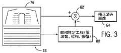
後にあらためて詳述するように、一般に、画像データに存在し得るEMI起源のアーティファクトは、画像データ(所望の画像データ及びEMI雑音の両方を含む)を取得し、このデータをEMI雑音を特性決定するように処理することにより特性決定することができ、次いで、これらのアーティファクトを除去すれば補正済み画像を得ることができるものと決定されている。以下で述べる現状で思量される実施形態では、画像データはオフセット・データと共に読み出されて、これらの読み出し動作の両方が、横列をイネーブル(すなわち「FET入」)にしてデータを読み出すことと、横列をディスエーブル(すなわち「FET切」)にしてデータを読み出すこととを含んでいる。かかる補正の全体的な図式を図3に線図で示す。 As will be described in more detail later, in general, EMI-derived artifacts that may be present in image data obtain image data (including both desired image data and EMI noise) and characterize this data for EMI noise. It has been determined that the processing can be characterized and then a corrected image can be obtained by removing these artifacts. In the presently contemplated embodiment described below, image data is read along with the offset data, and both of these read operations read the data with the row enabled (ie, “FET on”); Including reading the data with the row disabled (ie, “FET off”). The overall diagram of such correction is shown diagrammatically in FIG.
図3に示すように、工程の第一段階として、参照番号76によって示すようにX線画像データを取得する。このことは、上述の形式のディジタル検出器を用いて従来の態様で行なわれ得る。また、画像データは、被検体によるX線の減弱、散乱又は吸収によって生ずる検出器のフォトダイオードの電荷の消尽を読み出すために横列をイネーブルにして取得される。この読み出しに伴って、参照番号78によって全体的に示すようにEMI特性表現データを読み出す。この読み出しは、EMI起源の雑音(及びデータ処理に用いられるあらゆるオフセット)のみについての情報を得るために、横列をディスエーブルにして実行される。次いで、後者のデータセットを参照番号80によって示すEMI推定工程において用い、このときEMIデータが干渉を周波数、位相及び振幅について特性表現する。現状で思量される実施形態では、EMI特性表現データの取得は取得系列において画像データ取得の直後に行なわれるため、EMI特性表現データの位相は画像データの位相と同じになることが確実になる。次に、特性決定されたEMI成分を、加算器82によって示すように原画像データ(本工程によらなければEMI成分及びこれらの成分が生じ得るアーティファクトを含んでいたであろうもの)から減算して、補正済み画像データ84に到達する。この手法は、データにおけるEMI起源のアーティファクトの極めて正確な特性決定、これらのアーティファクトの除去、及び補正済みデータから再構成される大幅に画質向上した補正済み画像の提示を可能にすることが判明した。 As shown in FIG. 3, as a first stage of the process, X-ray image data is acquired as indicated by
以下、あらゆるEMI起源のアーティファクトを解消するためにEMIを特性決定すると共に画像データを補正するのに用いられるデータを収集することに対する特定的なアプローチについてさらに詳細に説明する。但し、以下の議論を通じて特性決定の目的でのEMIの解析に対するアプローチが提示される。本発明によれば、一旦画像データ及びEMI特性表現データが取得されて記憶されたら、次いで、このアプローチをEMIの特性決定に用いる。このことについて以下で詳述する。 In the following, a specific approach to collecting data used to characterize EMI and correct image data to resolve any EMI-origin artifact will be described in more detail. However, the following discussion presents an approach to EMI analysis for characterization purposes. In accordance with the present invention, once image data and EMI characteristic representation data have been acquired and stored, this approach is then used for EMI characteristic determination. This will be described in detail below.
EMIは、時間領域におけるシヌソイド型信号として記述することができる。画像の各々の横列に位置する全ピクセルについてのデータが同時に取得されるので、これらのデータは、同じ位相のEMIによる影響を受ける。殆どの臨床画像に見られるようにEMIの強度が検出器全体にわたって同じである場合には、摂動の程度は画像の横列1列に位置する全ピクセルについて同じである。 EMI can be described as a sinusoidal signal in the time domain. Since data for all pixels located in each row of the image is acquired simultaneously, these data are affected by the same phase of EMI. If the intensity of EMI is the same across the detector as seen in most clinical images, the degree of perturbation is the same for all pixels located in one row of the image.
このように、EMIによるアーティファクトは、画像の各々の横列に位置するピクセル値を平均することにより得られ、測定システムによって導入される無作為型の加算的雑音を低減することができる。EMI強度が検出器にわたって区々である場合には、平均演算を横列全体にわたって実行することができない。この場合には、画像を複数のROI(関心領域)に分割し、次いでこれらのROIの各々について平均を施すものとする。後述するように、現状で思量されるアプローチは、2048×2048ピクセルの画像を24区画のROIに分解するが、それでもこのアプローチは各々のROIについて局所的にEMIの影響を特性決定して補正する。 In this way, EMI artifacts are obtained by averaging the pixel values located in each row of the image and can reduce the random additive noise introduced by the measurement system. If the EMI intensity varies across the detectors, the averaging operation cannot be performed across the entire row. In this case, the image is divided into a plurality of ROIs (regions of interest), and then an average is applied to each of these ROIs. As will be discussed later, the currently conceived approach decomposes a 2048 x 2048 pixel image into 24 compartment ROIs, but this approach still characterizes and corrects the effects of EMI locally for each ROI. .
EMIアーティファクトは一般的にはシヌソイド型信号であるので、画像におけるアーティファクトのコントラストはシヌソイドの振幅によって決定される。アーティファクトのコントラストを推定する問題は、シヌソイドの振幅の推定となる。fEMI及びaEMIをそれぞれそれぞれシヌソイドの周波数及び振幅とすると、次式によってアーティファクトを記述することができる。Since EMI artifacts are typically sinusoidal signals, the contrast of the artifact in the image is determined by the amplitude of the sinusoid. The problem of estimating artifact contrast is the estimation of sinusoid amplitude. If fEMI and aEMI are respectively the frequency and amplitude of the sinusoid, the artifact can be described by the following equation.

また、多数の走査線についてのアーティファクトを、 Also, artifacts for many scan lines
式(4)のコスト関数C1をaEMIに関して最小化すると、aEMIの推定値が得られる。Minimizing the cost function C1 of equation (4) with respect to aEMI yields an estimate of aEMI .
式(5)を式(4)に代入することにより、 By substituting equation (5) into equation (4),
ゆえに、fEMIを、Therefore, fEMI
一旦、 Once
尚、上述のFFTからの周波数推定値の分解能は、横列の列数Nによって制限され得ることを特記しておく。幾つかの例では、このことがアーティファクトを補正するのに十分に正確であるとは考えられない場合がある。この場合には、FFTを実行する前のデータ列にゼロを充填する[y(0),y(1),…,y(N−1),0,…,0]ことにより分解能を高めてもよいし、又はFFTから得られる初期周波数推定値の周囲で精密化探索を行なってもよい。次いで、精密化された周波数推定値によって式(9)からさらに正確な振幅推定値を更新する。 It should be noted that the resolution of the frequency estimation value from the above-described FFT can be limited by the number N of rows. In some instances, this may not be considered accurate enough to correct the artifact. In this case, the resolution is increased by filling the data string before executing FFT with zero [y (0), y (1),..., Y (N−1), 0,. Alternatively, a refinement search may be performed around the initial frequency estimate obtained from the FFT. The more accurate amplitude estimate is then updated from equation (9) with the refined frequency estimate.
EMIが多数の周波数から成っている場合には同様にして振幅を計算し得ることを示すことができる。ピークが周波数領域において十分に分離されている場合には、各々のピークの高さが周波数の各々の振幅を与える。二つの周波数が周波数領域において接近し過ぎていて分離することができない場合には、これらの周波数の振幅は、得られるシヌソイドをデータ列[y(0),y(1),…,y(N−1)]から除去することにより繰り返し式で得ることができる。 It can be shown that the amplitude can be calculated in the same way if the EMI consists of multiple frequencies. If the peaks are well separated in the frequency domain, the height of each peak gives the respective amplitude of the frequency. If the two frequencies are too close together in the frequency domain and cannot be separated, the amplitude of these frequencies can be obtained by converting the resulting sinusoid into the data string [y (0), y (1),..., Y (N -1)] can be obtained repeatedly.
上述のアプローチでは、シヌソイド振幅の最善の推定値を得ることができる。このアプローチは、検出器のパネル温度によるもののような変化し得る電子雑音には敏感でない。 With the above approach, the best estimate of the sinusoid amplitude can be obtained. This approach is not sensitive to variable electronic noise such as that due to detector panel temperature.
以上に述べた推定工程を、EMIの振幅及び周波数について用いることができる。後述するように、現状で思量されるアプローチにおいてはEMIの位相は重大ではない、というのは、EMIを特性決定するのに用いられるデータは本質的に、X線画像について収集されたデータと位相が揃っているからである。すなわち、以下で図4、図5、図6及び図7を参照して議論するように、EMI特性表現データは同じデータ取得系列又はプロトコルで取得されるが、この場合に横列をイネーブルにするFETを単純に切状態に切り換えておく。このように、EMIの特性決定をするときには、移相を考慮したり実行したりする必要なく単純にEMIを画像データから減算することができる。 The estimation process described above can be used for EMI amplitude and frequency. As will be discussed later, in the currently conceived approach, the EMI phase is not critical because the data used to characterize the EMI is essentially the data and phase collected for the X-ray image. This is because they are ready. That is, as discussed below with reference to FIGS. 4, 5, 6 and 7, EMI characterization data is acquired with the same data acquisition sequence or protocol, but in this case FETs that enable rows Is simply switched off. As described above, when determining the characteristics of EMI, it is possible to simply subtract EMI from image data without having to consider or execute phase shift.
尚、このEMI推定アプローチは、本書に記載した特性決定及び画像データ補正の具現化形態以外でも応用され得ることを特記しておく。例えば、シヌソイドの周波数及び振幅を画像取得時に実時間で計算し、EMIが存在する場合に警報信号を操作者へ送信するEMI監視システムがある。異なる観察者は異なる周波数のアーティファクトに対して異なる視覚感度を有するので、警報閾値も周波数依存性となる。さらに他の応用としては、X線画像のアーティファクトを低減する又は解消するようなkVp、mA、mAs、及びフィルタ処理等を含めた曝射手法についての干渉の周波数及び振幅に応じた調節等がある。さらにもう一つの応用としては、一旦、アーティファクトが閾値を上回ったら、検出器に遮蔽外殻のような遮蔽設備を設置するように操作者に警報を与えるもの等がある。 It should be noted that this EMI estimation approach can be applied to other than the implementation of characterization and image data correction described in this document. For example, there is an EMI monitoring system that calculates the frequency and amplitude of a sinusoid in real time at the time of image acquisition and transmits an alarm signal to an operator when EMI is present. Since different observers have different visual sensitivities for different frequency artifacts, the alarm threshold is also frequency dependent. Still other applications include adjustments according to the frequency and amplitude of interference for exposure techniques including kVp, mA, mAs, and filtering that reduce or eliminate X-ray image artifacts. . Yet another application is to warn the operator to install a shielding facility such as a shielding shell on the detector once the artifact exceeds a threshold.
空間の所与の点について、電磁干渉(EMI)を時間領域におけるK個のシヌソイドの和として記述することができる。 For a given point in space, electromagnetic interference (EMI) can be described as the sum of K sinusoids in the time domain.
干渉は、上述の検出器パネル及び読み出し回路を介してX線画像データに加算され、又はさらに一般的には影響を与える。具体的には、前述のように、パネルのピクセルは二次元マトリクスとして構成されており、1列の縦列がデータ線を介して特定の読み出し回路によって読み出される。ピクセル読み出しの順序及び時間的瞬間は走査線によって制御される。パネルの横列に位置するピクセルは、各々の横列が同時に読み出されるように1本の走査線によって接続されている。結果として、加算的な干渉が、画像の横列方向の線又は帯として見える横列相関雑音形式のアーティファクトとして現われる。 The interference is added to, or more generally affects, the X-ray image data via the detector panel and readout circuit described above. Specifically, as described above, the pixels of the panel are configured as a two-dimensional matrix, and one column is read out by a specific readout circuit via a data line. The order and temporal instants of pixel readout are controlled by the scan line. The pixels located in the rows of the panel are connected by one scan line so that each row is read out simultaneously. As a result, additive interference appears as artifacts in the form of row correlation noise that appear as rows or bands in the row direction of the image.
横列m及び縦列nに位置するピクセルの加算値は次式によって表わすことができ、 The sum of the pixels located in row m and column n can be expressed as:
ここで関心のある問題は、画像アーティファクト The issue of interest here is the image artifact
シヌソイド Sinusoid
FET入及びFET切の検出器からデータを取得することにより、画像の「拡張」横列(すなわち画像データの横列及びEMI特性表現データの横列)からのK個のシヌソイドの加算によって記述されるアーティファクトのパラメータの推定が可能になる。以下で記載する本発明の手法によればデータの一部はFET切で取得されるので、EMIが存在しない場合に同じ手法で得られるEMI不含オフセットから構造を容易に取り出すことができる。 By acquiring data from the FET on and FET off detectors, the artifacts described by the addition of K sinusoids from the “extended” row of images (ie, the row of image data and the row of EMI characterization data) The parameter can be estimated. According to the method of the present invention described below, a part of the data is acquired with the FET turned off, so that the structure can be easily extracted from the EMI-free offset obtained by the same method when EMI does not exist.
このように、{d0,d1,…,dM−1}が通常の画像に対応し、{dM,…,dM+L−1}がFET入及びFET切の横列のデータであるとして、{d0,d1,…,dM−1,dM,…,dM+L−1}が横列拡張画像から得られるベクトルである場合には、このベクトルは画像の1列の縦列又は幾列かの縦列の平均であり得る(但し現状で思量される実施形態では、それでも検出器の一部に局所化される)。新たなベクトルが、順序の反転した{dM,…,dM+L−1}を用いることにより、
e(l)=dM+L−1−l,l=0,1,…,L−1 (16)
のように定義される場合には、{dM−1,…,d1,d0}に含まれるシヌソイドは、ベクトルIn this way, {d0 , d1 ,..., DM−1 } corresponds to a normal image, and {dM ,..., DM + L−1 } is the row data with FET on and FET off. , {D0 , d1 ,..., DM−1 , dM ,..., DM + L−1 } is a vector obtained from a row extension image, this vector can be a column of images or It can be the average of a series of columns (although in the presently contemplated embodiment, it is still localized to a portion of the detector). The new vector uses {dM ,..., DM + L−1 } with reversed order,
e (l) = dM + L-1-l , l = 0, 1,..., L-1 (16)
, The sinusoid included in {dM−1 ,..., D1 , d0 } is a vector
この手法を具現化するためには、周波数推定値が正確であることが望ましい。例えば、M=L=2048とすると、画像の第一の横列のアーティファクトを補正するためには、 In order to implement this technique, it is desirable that the frequency estimate is accurate. For example, if M = L = 2048, to correct the first row of artifacts in the image,
上述のように、この補正アルゴリズムは、検出器において具現化することができる。また、検出器制御サーキットリ又はシステム制御サーキットリにおいて具現化することもできるし、遠隔コンピュータの後処理によって具現化することもできる。後者の場合には、画像データ及びEMI特性決定データを有する横列全体を処理サーキットリへ転送してもよいし、幾列かの縦列を平均した後に画像の未使用領域にベクトルを保存することにより、これらの合計横列の寸法を小さくしてもよい。例えば、画像の所定数の線(例えば画像境界の各々に位置する12本の線)を用いて、平均後の縦列ベクトルを記憶させることができる。この場合には、画像寸法は以前と同じになる。代替的には、画像の寸法を拡大してもよい。 As mentioned above, this correction algorithm can be implemented in a detector. It can also be implemented in a detector control circuit or a system control circuit, or by post-processing of a remote computer. In the latter case, the entire row with image data and EMI characterization data may be transferred to the processing circuitry, or by averaging several columns and storing the vector in an unused area of the image. The dimensions of these total rows may be reduced. For example, the averaged column vector can be stored using a predetermined number of lines of the image (eg, 12 lines located at each of the image boundaries). In this case, the image size is the same as before. Alternatively, the image dimensions may be enlarged.
また、全てのオフセット画像及びX線画像について画像アーティファクトを補正してもよい。EMIが存在しない場合には、シヌソイド型推定値の振幅は等しくなるか又はゼロに近くなる。このように、EMIが存在しない場合には、通常の画像取得及び処理を行なうことができる。EMIが検出されたときに、横列データ及びEMI特性表現データを伴う「拡張」画像を取得してEMI補正を施すことができる。さらにまた、横列データ及びEMI特性表現データについてのベクトルを画像の未使用領域に記憶させて、観察者(医療の状況では医師)が画像にアーティファクトを観察したときにEMI補正を実行してもよい。 In addition, image artifacts may be corrected for all offset images and X-ray images. In the absence of EMI, the amplitudes of the sinusoidal estimates are equal or close to zero. Thus, when EMI does not exist, normal image acquisition and processing can be performed. When EMI is detected, an “extended” image with row data and EMI characteristic representation data can be acquired and subjected to EMI correction. Furthermore, vectors for the row data and the EMI characteristic expression data may be stored in an unused area of the image, and EMI correction may be performed when an observer (a doctor in a medical situation) observes an artifact in the image. .
また、検出器品質検査又は検出器較正を介して定期的にEMI不含参照FET切画像を得ることができる。また、EMIが検出されていないときに横列データ及びEMI特性表現データを含む画像からEMI不含参照FET切画像を得ることもできる。最新で得られたEMI不含FET切画像を用いてもよいし、最新の数枚の画像を平均してもよい。平均画像を用いる場合には、単純平均又は加重平均を用いることができ、加重平均の場合には最新の画像に最大加重を与える。 Also, an EMI-free reference FET cut-out image can be obtained periodically through detector quality inspection or detector calibration. Further, when no EMI is detected, an EMI-free reference FET cut image can be obtained from an image including row data and EMI characteristic expression data. The latest obtained EMI-free FET cut image may be used, or the latest several images may be averaged. When using an average image, a simple average or a weighted average can be used, and in the case of a weighted average, the latest image is given the maximum weight.
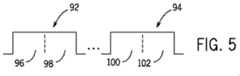
図4は、以上の原理に従ってEMIの特性決定及び画像データの補正を可能にするように設計された画像データ取得プロトコルの時間線を表わす。参照番号86によって全体的に示す時間線は、検出器スクラブ88、X線受光90、並びにデータ読み出し92及び94の各期間を含み得る。当業者には認められるように、検出器のフォトダイオードの電荷の不可避的損失に対処するために、電荷参照番号88によって示すスクラブ動作によってフォトダイオードを定期的に再充電すると有用であり得る。本質的に、かかる動作はダイオード電荷を刷新するが、電荷データを読み出すことはない。次いで、データ取得プロトコルの何らかの点において、受光期間90時に検出器にX線放射線が入射するようにX線源が起動される。X線放射線は各々のピクセル位置において、シンチレータの該当位置において受光されたX線放射線の量に対応する光検出器の電荷の消尽を生ずる。X線受光期間に続いて、参照番号92によって示すようなデータ読み出しが行なわれる。後述するように、この読み出し92は、本発明の手法によれば、EMIがシステムに存在するときには、有用な画像を再構成するのに用いられるデータばかりでなくEMIによる影響を受けた画像データの読み出しを含む。二次的な読み出し期間94では、かかるEMIが存在するときには同様にEMIによる影響を受けたオフセット・データが読み出される。 FIG. 4 represents a timeline of an image data acquisition protocol designed to allow EMI characterization and image data correction according to the above principles. The time line indicated generally by reference number 86 may include
図5は、これらの読み出し期間を幾分詳細に示している。上述のように、検出器の各横列はドライバ・サーキットリによって、典型的にはドライバ・サーキットリにおいて用いられる1又は複数のFETの状態を変化させることによりイネーブルにされる。次いで、横列からデータを読み出すために、FETサーキットリを入にしてかかる読み出しをイネーブルにする。本発明の手法によれば、期間92のデータ読み出しでは、第一の相96の間に各横列をイネーブルにすると、存在するあらゆるEMIによる影響を受ける画像データが読み出される。この同じ読み出し期間に、各横列をディスエーブル(すなわちFET切)にして、参照番号98に示すようにデータを取得する。このデータは、システムに存在するEMIの影響を受けているが、各横列をディスエーブルにしているため画像データは含まない。同様に、オフセット・データ読み出し期間94では、FETを入にして参照番号100に示すようにオフセット・データを読み出し、オフセット・データ及び対応するEMI特性表現データを収集する。続いて直ちに、横列ドライバ・サーキットリは横列をディスエーブル(すなわちFET切)にして読み出しを続行し、存在するEMIによる影響を受けた情報のみを収集する。 FIG. 5 shows these readout periods in some detail. As described above, each row of detectors is enabled by the driver circuitry, typically by changing the state of one or more FETs used in the driver circuitry. The FET circuitry is then turned on to enable such reading in order to read data from the row. According to the method of the present invention, in the data reading in the
収集されたデータを用いて、前述のように画像データから減算することができるようにEMIを特性決定する。画像データ、オフセット・データ及びEMI特性表現データを読み出す期間の持続時間は様々であってよく、これらの期間は互いに等しいか又は典型的にはEMI特性表現データ読み出しが短い。但し、所望に応じてこの期間が長くなってもよい。一般的には、読み出しが行なわれる持続時間は、検出器の横列の列数によって既知である。次いで、読み出し期間96は、X線信号、オフセット信号(線入)及びEMI信号に関連するデータを取得する。一方、期間98に取得される画像データは、オフセット(線切)及びEMIに関連するデータを含む。同様に、期間100に取得されるデータは、オフセット・データ(線入)及びEMIデータを含み、データ取得期間102はオフセット・データ(線切)及びEMIデータを含む。 The collected data is used to characterize the EMI so that it can be subtracted from the image data as described above. The duration of reading the image data, offset data and EMI characteristic representation data may vary, and these periods are equal to each other or typically the EMI characteristic expression data reading is short. However, this period may be lengthened as desired. In general, the duration of the readout is known by the number of rows in the detector row. Next, in the
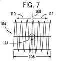
上述のように、現状で思量される実施形態では、EMI特性表現データの取得は前段の読み出し系列に続いて直ちに行なわれる。これにより、EMI特性表現データの位相が直前に読み出された画像データ又はオフセット・データの位相と確実に揃う。図6及び図7は、この点を示すEMIアーティファクト・トレースを示す。時間線に沿って、アーティファクト・トレースは、再構成画像に線として重ね合わされる明暗のある区画として現われる。アーティファクト・トレース104をFET切の切り換え窓106において拡大することができ、図7では図6に比較して拡大されている。画像取得時には、時刻108にドライバ・サーキットリFETを切に切り換えることにより各横列を単純にディスエーブルにする。図6及び図7に示す実施形態では、例えば、2048×2048ピクセル検出器の読み出しは線2048の読み出しの後にFETを切に切り換える。すると、FET切の切り換えによって、トレースがFET入時間110及びFET切時間112に分割される。しかしながら、図7に最も分かり易く示すように、アーティファクト・トレース104はこの切り換えを通じて連続しており、FETの切り換えの前及び後の両方で位相が揃ったままになることを示している。 As described above, in the presently conceived embodiment, the acquisition of the EMI characteristic expression data is performed immediately following the preceding read sequence. This ensures that the phase of the EMI characteristic expression data is aligned with the phase of the image data or offset data read immediately before. 6 and 7 show EMI artifact traces that illustrate this point. Along the time line, the artifact traces appear as light and dark sections that are superimposed as lines on the reconstructed image.
このように、以上に述べた手法は、図5の期間96及び100に取得されたデータ(EMIによる影響を受けたX線画像データ単独の決定を可能にする)、並びに期間98及び102に収集されたデータからのEMI(位相の連続性によるオフセットの相殺による)に基づいて、EMIの周波数及び振幅の特性決定を可能にする。次いで、EMIによる影響を受けたX線画像と特性決定されたEMIとの間の差によって補正済みX線画像データをレンダリングする。オフセット単独の除去では位相差のためEMI成分を除去することはできないことを特記しておく。実際に、位相差はアーティファクトの影響を現実には強化してしまう場合がある。 Thus, the technique described above collects data acquired during
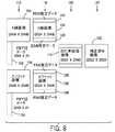
上述のように、本書に記載したEMI特性決定及び画像補正アプローチを具現化するために様々なデータ処理アプローチが思量される。図8は、具現化形態の一例を示しており、ここでは特性表現データが、処理時に画像の空き横列に一時的に配置されている。図8に示す実施形態では、参照番号116は検出器ファームウェアに存在するものとしての画像データを示し、参照番号118は検出器ソフトウェアに存在するものとしての画像データを示し、参照番号120はIDCソフトウェアに存在するものとしての画像データを示し、参照番号122は後処理のために存在する補正済み画像データを表わしている。検出器では、上述のように、X線画像データ124は第一の読み出し期間に収集され、FET切データ126がこの直後に収集される。データは、EMIを特性決定するために検出器の全ての領域について収集されてもよいが、図8に示す実施形態では、群を成す縦列(例えば85列の縦列)を平均して単一の縦列とすると、EMI特性表現データ126において24列のデータの縦列が得られる。同様に、オフセット画像データ128はオフセット・データ収集期間に収集されて、直後にFET切データ130の収集が行なわれる。ここでもやはり、EMI特性表現データをまとめて24列の縦列にする。尚、データを複数の縦列にまとめても、検出器にわたるEMIの影響は局所化されることを特記しておく。実用では、さらに多数の縦列又はさらに少数の縦列をまとめて、これらの影響のさらに十分な局所化又はさらに少ない局所化を提供することができる。 As mentioned above, various data processing approaches are contemplated to implement the EMI characterization and image correction approaches described herein. FIG. 8 shows an example of an embodiment, in which the characteristic expression data is temporarily arranged in empty rows of the image during processing. In the embodiment shown in FIG. 8,
図8の参照番号118によって示すように、検出器ソフトウェアでは、FET切データはX線画像データ132の最上部及び最下部の領域134に簡便に記憶され、FET切は同様に、オフセット画像データ136の周りの空き領域138に記憶される。このデータは最終的には、IDCソフトウェアの未処理データセット140として記憶されて、EMIの特性決定及びその影響の補正に続いて補正済み画像142が形成される。他の画像処理の方式及びアプローチは言うまでもなく当業者には明らかであろう。最終的には、補正済み画像データはイメージング・システム自体のメモリ・サーキットリ等に記憶され、これらのデータを用いて有用な画像を再構成する。かかる画像は、上述の形式のモニタにおいて観察されてもよいし、フィルム等に印刷、転送されてもよい。また、取得されたデータの任意のものを後の処理又は参照のために記憶させてもよい。補正済み画像の実時間又は近実時間での観察が必要でない場合には、EMI特性決定及び補正工程の全体を後に実行してもよいし、さらにはイメージング・システムから遠隔で実行してもよい。 As indicated by
図9は、上述のように検出器を複数の領域に分割することによる検出器にわたるEMIの影響の局所化を表わしている。図9に示すように、検出器60は縦列58及び横列56を成すピクセル54を含んでおり、参照番号144によって示すようにまとめられた一連の縦列に分割され得る。EMI特性表現データは、この縦列の群について記憶され得る。この場合にも、さらに局所化されたEMIの特性決定が望ましい場合には、これらの群をさらに小さくすればよい。次いで、前述のようにこれらの局所化された群についてEMI特性決定及び補正が実行される。 FIG. 9 represents the localization of EMI effects across the detector by dividing the detector into multiple regions as described above. As shown in FIG. 9, the
本発明の技術的効果としては、EMIを推定して特性決定する能力、及びこの情報を用いてラジオグラフィ・システムを介して取得された画像データを補正する能力等がある。これらの効果は、後処理ばかりでなく近実時間(画像データが取得されている最中又はその短時間後)でかかるタスクを実行する能力にも拡張される。このようにして、改善された再構成画像が、画像データに対するEMIの影響の低減によって入手可能となる。 Technical effects of the present invention include the ability to estimate and characterize EMI and the ability to correct image data acquired via a radiography system using this information. These effects extend not only to post-processing, but also to the ability to perform such tasks in near real time (while image data is being acquired or shortly thereafter). In this way, an improved reconstructed image can be obtained by reducing the influence of EMI on the image data.
本書では発明の幾つかの特徴のみを図示して説明したが、当業者には多くの改変及び変形が想到されよう。従って、特許請求の範囲は、本発明の要旨に含まれるような全ての改変及び変形を網羅するものと理解されたい。 While only certain features of the invention have been illustrated and described herein, many modifications and changes will occur to those skilled in the art. Therefore, it is to be understood that the claims are intended to cover all modifications and variations as fall within the spirit of the invention.
10 イメージング・システム
12 X線放射線
14 コリメータ
16 放射線
18 被検体
20 放射線
22 検出器
24 電源/制御回路
26 検出器制御器
28 システム制御器
30 表示器/プリンタ
32 操作者ワークステーション
34 IDC
36 検出器制御回路
38 電源
40 参照/調節器回路
42 横列バス
44 縦列バス
46 横列ドライバ
48 読み出し電子回路
50 検出器パネル
52 区画
54 ピクセル
56 横列
58 縦列
60 画像マトリクス
62 高さ
64 幅
68 縦列電極
70 横列電極
72 薄膜トランジスタ
74 フォトダイオード
76 X線画像データ
78 EMI特性決定データ
80 EMI推定工程
82 加算器
84 補正済み画像データ
86 画像プロトコル時間線
88 スクラブ期間
90 X線受光
92 データ読み出し
94 オフセット・データ読み出し
96 横列イネーブル時画像データ読み出し
98 横列ディスエーブル時読み出し
100 横列イネーブル時読み出し
102 横列ディスエーブル時読み出し
104 アーティファクト・トレース
106 FET切の切り換え窓
108 FET切への切り換え
110 信号の連続性
112 FET入
114 FET切
116 検出器ファームウェアの画像データ
118 検出器ソフトウェアの画像データ
120 IDCソフトウェアの画像データ
122 後処理用の補正済み画像データ
124 第一の読み出し期間に収集されたX線画像データ
126 FET切データ
128 オフセット画像データ
130 FET切データ
132 X線画像データ
134 空き領域
136 オフセット画像データ
138 空き領域
140 未処理データ集合
142 補正済み画像
144 まとめた縦列DESCRIPTION OF
36
Claims (10)
Translated fromJapanese電磁干渉により生ずるデータ(78)を含むがX線画像データは含まない第二のデータを、前記ディジタル検出器(22)を介して取得するステップ(98)と、
少なくとも前記第二のデータに基づいて前記電磁干渉を推定するステップ(80)と、
前記特性決定された電磁干渉に基づいて前記第一のデータを補正するステップ(84)と
を備えたX線画像データを処理するコンピュータ利用型方法。Obtaining (96) first data including X-ray image data (76) and data (78) resulting from electromagnetic interference via a digital detector (22);
Acquiring (98) via the digital detector (22) second data including data (78) resulting from electromagnetic interference but not X-ray image data;
Estimating the electromagnetic interference based on at least the second data (80);
A computer-based method of processing X-ray image data comprising correcting (84) the first data based on the characterized electromagnetic interference.
Applications Claiming Priority (1)
| Application Number | Priority Date | Filing Date | Title |
|---|---|---|---|
| US12/124,355US7649979B2 (en) | 2008-05-21 | 2008-05-21 | Artifact reduction system and method for radiological imaging system |
Publications (1)
| Publication Number | Publication Date |
|---|---|
| JP2009279408Atrue JP2009279408A (en) | 2009-12-03 |
Family
ID=41342115
Family Applications (1)
| Application Number | Title | Priority Date | Filing Date |
|---|---|---|---|
| JP2009120506APendingJP2009279408A (en) | 2008-05-21 | 2009-05-19 | System and method of reducing artifact for radiation imaging system |
Country Status (2)
| Country | Link |
|---|---|
| US (1) | US7649979B2 (en) |
| JP (1) | JP2009279408A (en) |
Cited By (3)
| Publication number | Priority date | Publication date | Assignee | Title |
|---|---|---|---|---|
| JP2012517168A (en)* | 2009-02-06 | 2012-07-26 | トリクセル エス.アー.エス. | Method for correcting an image acquired by an array of photosensitive spots |
| JP2014100394A (en)* | 2012-11-21 | 2014-06-05 | Canon Inc | Radiological imaging device, method for controlling the same, and program |
| JP2015047371A (en)* | 2013-09-02 | 2015-03-16 | 株式会社東芝 | X-ray image processor, x-ray diagnostic apparatus and x-ray image processing program |
Families Citing this family (14)
| Publication number | Priority date | Publication date | Assignee | Title |
|---|---|---|---|---|
| US8786873B2 (en) | 2009-07-20 | 2014-07-22 | General Electric Company | Application server for use with a modular imaging system |
| JP5627275B2 (en)* | 2010-04-21 | 2014-11-19 | キヤノン株式会社 | Image processing apparatus, image processing method, and program |
| US8243882B2 (en) | 2010-05-07 | 2012-08-14 | General Electric Company | System and method for indicating association between autonomous detector and imaging subsystem |
| US8384041B2 (en)* | 2010-07-21 | 2013-02-26 | Carestream Health, Inc. | Digital radiographic imaging arrays with reduced noise |
| JP5767459B2 (en)* | 2010-11-29 | 2015-08-19 | キヤノン株式会社 | Radiation imaging apparatus, control method thereof, control system, and program |
| US8781075B2 (en) | 2011-01-07 | 2014-07-15 | General Electric Company | Wireless communication in a medical imaging or monitoring system |
| US8693747B2 (en)* | 2011-04-29 | 2014-04-08 | General Electric Company | Radiological image noise reduction system and method |
| US9107604B2 (en)* | 2011-09-26 | 2015-08-18 | Given Imaging Ltd. | Systems and methods for generating electromagnetic interference free localization data for an in-vivo device |
| US9101316B2 (en) | 2011-11-30 | 2015-08-11 | General Electric Company | Portable radiation detector and system |
| DE102014205841A1 (en)* | 2014-03-28 | 2015-05-21 | Siemens Aktiengesellschaft | Image processing method for removing bright-burn artifacts and X-ray machine |
| US10588542B2 (en) | 2014-07-10 | 2020-03-17 | Given Imaging Ltd. | Sensor belt configured to localize an in-vivo device and method for localization |
| US10828003B2 (en)* | 2019-03-18 | 2020-11-10 | GE Precision Healthcare, LLC | System and method for mitigating electromagnetic interference when acquiring image data |
| US11259770B2 (en)* | 2019-11-14 | 2022-03-01 | GE Precision Healthcare LLC | Methods and systems for noise reduction in x-ray imaging |
| CN115825597A (en)* | 2021-09-15 | 2023-03-21 | 英业达科技有限公司 | Electromagnetic sensitivity test method based on computer vision |
Citations (1)
| Publication number | Priority date | Publication date | Assignee | Title |
|---|---|---|---|---|
| US20080025474A1 (en)* | 2006-07-21 | 2008-01-31 | Anton Nekovar | Method for operating a diagnostic apparatus with an x-ray system and a position determination system for catheters together with diagnostic apparatus for performance of the method |
- 2008
- 2008-05-21USUS12/124,355patent/US7649979B2/ennot_activeExpired - Fee Related
- 2009
- 2009-05-19JPJP2009120506Apatent/JP2009279408A/enactivePending
Patent Citations (1)
| Publication number | Priority date | Publication date | Assignee | Title |
|---|---|---|---|---|
| US20080025474A1 (en)* | 2006-07-21 | 2008-01-31 | Anton Nekovar | Method for operating a diagnostic apparatus with an x-ray system and a position determination system for catheters together with diagnostic apparatus for performance of the method |
Cited By (3)
| Publication number | Priority date | Publication date | Assignee | Title |
|---|---|---|---|---|
| JP2012517168A (en)* | 2009-02-06 | 2012-07-26 | トリクセル エス.アー.エス. | Method for correcting an image acquired by an array of photosensitive spots |
| JP2014100394A (en)* | 2012-11-21 | 2014-06-05 | Canon Inc | Radiological imaging device, method for controlling the same, and program |
| JP2015047371A (en)* | 2013-09-02 | 2015-03-16 | 株式会社東芝 | X-ray image processor, x-ray diagnostic apparatus and x-ray image processing program |
Also Published As
| Publication number | Publication date |
|---|---|
| US20090290686A1 (en) | 2009-11-26 |
| US7649979B2 (en) | 2010-01-19 |
Similar Documents
| Publication | Publication Date | Title |
|---|---|---|
| JP2009279408A (en) | System and method of reducing artifact for radiation imaging system | |
| CN102783958B (en) | Radiation image noise decrease system and method | |
| JP5738510B2 (en) | Image acquisition and processing chain for dual energy radiation imaging using a portable flat panel detector | |
| KR101576703B1 (en) | Image processing apparatus, image processing method, and computer-readable storage medium | |
| US9194965B2 (en) | System and method for X-ray image acquisition and processing | |
| CN111184523B (en) | Three-dimensional image reconstruction method and system based on DR equipment | |
| KR20170094196A (en) | Beam detection with continuous detector readout | |
| JP6744764B2 (en) | Image diagnostic apparatus and image acquisition method | |
| CN111353962B (en) | Method for reducing artifacts, X-ray device and electronically readable data carrier | |
| JP2012075099A (en) | Digital X-ray detector with expanded dynamic range | |
| JP2016202219A (en) | Radiographic imaging system and body thickness estimation method | |
| JP5823208B2 (en) | X-ray computed tomography system | |
| WO2014025903A1 (en) | Gain calibration technique for digital imaging systems | |
| US11431928B2 (en) | System and method for mitigating electromagnetic interference when acquiring image data | |
| JP5844517B2 (en) | System and method for erasing image artifacts | |
| US20130003912A1 (en) | System and method of acquiring computed tomography data using a multi-energy x-ray source | |
| EP2989983B1 (en) | Image processing device | |
| KR20110020969A (en) | Method and apparatus for removing image artifacts caused by defective pixels of flat panel X-ray detector in tomography system and tomography system | |
| WO2006006100A1 (en) | System and method for the correction of temporal artifacts in tomographic images | |
| JP5362282B2 (en) | X-ray diagnostic equipment | |
| JP5942216B2 (en) | X-ray CT apparatus and image processing apparatus | |
| JP6510729B2 (en) | Radiation image capturing system, image processing apparatus, radiation image capturing apparatus, image processing method, and image processing program | |
| JP5514397B2 (en) | Image display apparatus and X-ray tomography apparatus | |
| JP2025084082A (en) | Material weighting for projection spectral X-ray imaging | |
| CN202950665U (en) | Image system used for obtaining and handling discrete pixel image data |
Legal Events
| Date | Code | Title | Description |
|---|---|---|---|
| A621 | Written request for application examination | Free format text:JAPANESE INTERMEDIATE CODE: A621 Effective date:20120514 | |
| A977 | Report on retrieval | Free format text:JAPANESE INTERMEDIATE CODE: A971007 Effective date:20130513 | |
| A131 | Notification of reasons for refusal | Free format text:JAPANESE INTERMEDIATE CODE: A131 Effective date:20130521 | |
| A02 | Decision of refusal | Free format text:JAPANESE INTERMEDIATE CODE: A02 Effective date:20131029 |