JP2009273260A - Non-contact power transmission apparatus, power transmission apparatus and electronic apparatus using the same - Google Patents
Non-contact power transmission apparatus, power transmission apparatus and electronic apparatus using the sameDownload PDFInfo
- Publication number
- JP2009273260A JP2009273260AJP2008122270AJP2008122270AJP2009273260AJP 2009273260 AJP2009273260 AJP 2009273260AJP 2008122270 AJP2008122270 AJP 2008122270AJP 2008122270 AJP2008122270 AJP 2008122270AJP 2009273260 AJP2009273260 AJP 2009273260A
- Authority
- JP
- Japan
- Prior art keywords
- power transmission
- coil
- temperature
- primary coil
- temperature rise
- Prior art date
- Legal status (The legal status is an assumption and is not a legal conclusion. Google has not performed a legal analysis and makes no representation as to the accuracy of the status listed.)
- Pending
Links
- 230000005540biological transmissionEffects0.000titleclaimsabstractdescription112
- 230000002159abnormal effectEffects0.000claimsabstractdescription46
- 238000001514detection methodMethods0.000claimsabstractdescription42
- 238000006243chemical reactionMethods0.000claimsdescription4
- 230000020169heat generationEffects0.000abstractdescription7
- 238000011109contaminationMethods0.000abstractdescription2
- 239000000758substrateSubstances0.000description22
- WABPQHHGFIMREM-UHFFFAOYSA-Nlead(0)Chemical compound[Pb]WABPQHHGFIMREM-UHFFFAOYSA-N0.000description19
- 230000001681protective effectEffects0.000description11
- 238000010586diagramMethods0.000description8
- 230000008859changeEffects0.000description6
- 230000000630rising effectEffects0.000description6
- 230000004308accommodationEffects0.000description5
- 239000000463materialSubstances0.000description5
- 230000005856abnormalityEffects0.000description4
- 230000008878couplingEffects0.000description4
- 238000010168coupling processMethods0.000description4
- 238000005859coupling reactionMethods0.000description4
- 230000004907fluxEffects0.000description4
- 239000000696magnetic materialSubstances0.000description4
- 230000015572biosynthetic processEffects0.000description3
- 230000007423decreaseEffects0.000description3
- 230000000694effectsEffects0.000description3
- 230000005674electromagnetic inductionEffects0.000description3
- 230000017525heat dissipationEffects0.000description3
- 239000002184metalSubstances0.000description3
- 239000003990capacitorSubstances0.000description2
- 230000004048modificationEffects0.000description2
- 238000012986modificationMethods0.000description2
- 230000009471actionEffects0.000description1
- 230000001934delayEffects0.000description1
- 230000003111delayed effectEffects0.000description1
- 230000000149penetrating effectEffects0.000description1
- 229920001690polydopaminePolymers0.000description1
- 230000008054signal transmissionEffects0.000description1
- 238000005476solderingMethods0.000description1
- 125000006850spacer groupChemical group0.000description1
- 239000000126substanceSubstances0.000description1
- 238000004804windingMethods0.000description1
- 229910000859α-FeInorganic materials0.000description1
Images


Classifications
- H—ELECTRICITY
- H01—ELECTRIC ELEMENTS
- H01F—MAGNETS; INDUCTANCES; TRANSFORMERS; SELECTION OF MATERIALS FOR THEIR MAGNETIC PROPERTIES
- H01F38/00—Adaptations of transformers or inductances for specific applications or functions
- H01F38/14—Inductive couplings
- H—ELECTRICITY
- H02—GENERATION; CONVERSION OR DISTRIBUTION OF ELECTRIC POWER
- H02J—CIRCUIT ARRANGEMENTS OR SYSTEMS FOR SUPPLYING OR DISTRIBUTING ELECTRIC POWER; SYSTEMS FOR STORING ELECTRIC ENERGY
- H02J50/00—Circuit arrangements or systems for wireless supply or distribution of electric power
- H02J50/005—Mechanical details of housing or structure aiming to accommodate the power transfer means, e.g. mechanical integration of coils, antennas or transducers into emitting or receiving devices
- H—ELECTRICITY
- H02—GENERATION; CONVERSION OR DISTRIBUTION OF ELECTRIC POWER
- H02J—CIRCUIT ARRANGEMENTS OR SYSTEMS FOR SUPPLYING OR DISTRIBUTING ELECTRIC POWER; SYSTEMS FOR STORING ELECTRIC ENERGY
- H02J50/00—Circuit arrangements or systems for wireless supply or distribution of electric power
- H02J50/10—Circuit arrangements or systems for wireless supply or distribution of electric power using inductive coupling
- H02J50/12—Circuit arrangements or systems for wireless supply or distribution of electric power using inductive coupling of the resonant type
- H—ELECTRICITY
- H02—GENERATION; CONVERSION OR DISTRIBUTION OF ELECTRIC POWER
- H02J—CIRCUIT ARRANGEMENTS OR SYSTEMS FOR SUPPLYING OR DISTRIBUTING ELECTRIC POWER; SYSTEMS FOR STORING ELECTRIC ENERGY
- H02J50/00—Circuit arrangements or systems for wireless supply or distribution of electric power
- H02J50/60—Circuit arrangements or systems for wireless supply or distribution of electric power responsive to the presence of foreign objects, e.g. detection of living beings
- H—ELECTRICITY
- H02—GENERATION; CONVERSION OR DISTRIBUTION OF ELECTRIC POWER
- H02J—CIRCUIT ARRANGEMENTS OR SYSTEMS FOR SUPPLYING OR DISTRIBUTING ELECTRIC POWER; SYSTEMS FOR STORING ELECTRIC ENERGY
- H02J50/00—Circuit arrangements or systems for wireless supply or distribution of electric power
- H02J50/90—Circuit arrangements or systems for wireless supply or distribution of electric power involving detection or optimisation of position, e.g. alignment
- H—ELECTRICITY
- H01—ELECTRIC ELEMENTS
- H01F—MAGNETS; INDUCTANCES; TRANSFORMERS; SELECTION OF MATERIALS FOR THEIR MAGNETIC PROPERTIES
- H01F27/00—Details of transformers or inductances, in general
- H01F27/40—Structural association with built-in electric component, e.g. fuse
- H01F27/402—Association of measuring or protective means
- H01F2027/406—Temperature sensor or protection
Landscapes
- Engineering & Computer Science (AREA)
- Power Engineering (AREA)
- Computer Networks & Wireless Communication (AREA)
- Charge And Discharge Circuits For Batteries Or The Like (AREA)
- Secondary Cells (AREA)
Abstract
Translated fromJapaneseDescription
Translated fromJapanese本発明は、無接点電力伝送に好適な送電装置およびその送電装置を用いた電子機器等に関する。 The present invention relates to a power transmission device suitable for contactless power transmission, an electronic device using the power transmission device, and the like.
電磁誘導を利用し、金属部分の接点がなくても電力送信を可能にする無接点電力伝送が知られている。この無接点電力伝送の適用例として、携帯電話の充電や家庭用機器(たとえば電話機の子機)の充電などが提案されている。 Contactless power transmission is known that uses electromagnetic induction to enable power transmission even without a metal part contact. As an application example of this non-contact power transmission, charging of a mobile phone or charging of household equipment (for example, a handset of a telephone) has been proposed.
無接点電力伝送の従来技術として特許文献1がある。この特許文献1では、送電ドライバの出力に接続された共振コンデンサと一次コイルとにより直列共振回路を構成して、送電装置(一次側)から受電装置(二次側)に電力を供給している。 There exists patent document 1 as a prior art of non-contact electric power transmission. In Patent Document 1, a series resonance circuit is configured by a resonance capacitor and a primary coil connected to an output of a power transmission driver, and power is supplied from a power transmission device (primary side) to a power reception device (secondary side). .
近年、携帯電話においては小型化が益々求められている。それに伴い、電力伝送を行うコイルユニットのより小型化、特に薄型化が必要となっている。
例えば無接点電力伝送では、一次コイル及びコイル間に金属等の異物が介在すると、この異物に渦電流が形成されて発熱する。 For example, in contactless power transmission, when a foreign object such as a metal is interposed between the primary coil and the coil, an eddy current is formed in the foreign object to generate heat.
本発明の幾つかの態様では、異物混入等の異常発熱を検出することができる送電装置及びそれを用いた電子機器を提供することができる。 In some aspects of the present invention, it is possible to provide a power transmission device capable of detecting abnormal heat generation such as contamination of foreign matter and an electronic device using the power transmission device.
本発明の一態様は、一次コイルを含み、前記一次コイルを受電装置の二次コイルと電磁的に結合させて、前記受電装置の負荷に対して電力を供給する送電装置において、前記一次コイルに交流信号を供給する送電部と、前記一次コイルの磁力線形成領域に配置される温度検出素子と、前記温度検出素子にて検出される第1の時刻の温度である第1の温度と第2の時刻の温度である第2の温度とに基づいて、異常温度上昇を検出する異常温度上昇検出部と、前記送電部を送電制御し、前記異常温度上昇検出部にて前記異常温度上昇が検出された時に前記一次コイルからの送電を停止制御する送電制御部と、を有することを特徴とする。 One embodiment of the present invention includes a primary coil, wherein the primary coil is electromagnetically coupled to a secondary coil of a power receiving device to supply power to a load of the power receiving device. A power transmission unit that supplies an AC signal, a temperature detection element that is disposed in a magnetic force line forming region of the primary coil, a first temperature that is a temperature at a first time detected by the temperature detection element, and a second temperature Based on the second temperature that is the temperature at the time, the abnormal temperature rise detection unit that detects an abnormal temperature rise, and the power transmission unit are controlled to transmit power, and the abnormal temperature rise detection unit detects the abnormal temperature rise. And a power transmission control unit for stopping and controlling power transmission from the primary coil.
本発明の一態様では、一次コイルの磁力線形成領域に異物が存在した時、その異物に生ずる渦電流に基づく異常発熱を検出して、送電を停止することができる。その異常発熱を検出するために、一次コイルの磁力線形成領域に温度検出素子が配置されている。さらに、異常発熱を判定するために、絶対温度を判定するのでなく、異常温度上昇を判定している。この異常温度上昇は、温度検出素子にて検出される第1の温度と第2の温度とに基づいて検出できる。 In one aspect of the present invention, when a foreign object exists in the magnetic field line formation region of the primary coil, abnormal heat generation based on an eddy current generated in the foreign object can be detected and power transmission can be stopped. In order to detect the abnormal heat generation, a temperature detection element is arranged in the magnetic force line forming region of the primary coil. Furthermore, in order to determine abnormal heat generation, the absolute temperature rise is determined instead of the absolute temperature. This abnormal temperature rise can be detected based on the first temperature and the second temperature detected by the temperature detection element.
本発明の一態様では、前記温度検出素子は、温度によって抵抗値が変化する可変抵抗素子とすることができる。この種の可変抵抗素子の代表例として、サーミスタを挙げることができる。 In one aspect of the present invention, the temperature detection element may be a variable resistance element whose resistance value varies with temperature. A typical example of this type of variable resistance element is a thermistor.
本発明の一態様では、前記異常温度上昇検出部は、前記可変抵抗素子によって変化する前記第1の時刻の電圧である第1の電圧と前記第2の時刻の電圧である第2の電圧に基づいて、前記異常温度上昇を検出することができる。可変抵抗素子の抵抗値の変化に基づいて電圧が変化するので、第1の時刻と第2の時刻との間での電圧の変化が温度上昇を示すことになる。 In one aspect of the present invention, the abnormal temperature rise detection unit generates a first voltage that is a voltage at the first time and a second voltage that is a voltage at the second time, which are changed by the variable resistance element. Based on this, the abnormal temperature rise can be detected. Since the voltage changes based on the change in the resistance value of the variable resistance element, the change in voltage between the first time and the second time indicates an increase in temperature.
本発明の一態様では、前記異常温度上昇検出部は、前記可変抵抗素子の可変抵抗値を周波数変換する抵抗値−周波数変換回路を含み、前記可変抵抗値によって変化する前記第1の時刻の周波数である第1の周波数と前記第2の時刻の周波数である第2の周波数を比較した結果に基づいて、前記異常温度上昇を検出することができる。例えば、可変抵抗素子の可変抵抗値と容量とでRC回路を構成すれば、抵抗の変化が周波数の変化として得られる抵抗値−周波数変換回路を構成できる。可変抵抗素子の抵抗値の変化に基づいて周波数が変化するので、第1の時刻と第2の時刻との間での周波数の変化が温度上昇を示すことになる。 In one aspect of the present invention, the abnormal temperature rise detection unit includes a resistance value-frequency conversion circuit that frequency-converts the variable resistance value of the variable resistance element, and the frequency at the first time that varies according to the variable resistance value. The abnormal temperature rise can be detected based on the result of comparing the first frequency that is and the second frequency that is the frequency at the second time. For example, if an RC circuit is configured with a variable resistance value and a capacitance of a variable resistance element, a resistance value-frequency conversion circuit in which a change in resistance is obtained as a change in frequency can be configured. Since the frequency changes based on the change in the resistance value of the variable resistance element, the change in frequency between the first time and the second time indicates an increase in temperature.
本発明の一態様は、前記異常温度上昇検出部は、前記温度検出素子にて検出される前記第1の温度と前記第2の温度との差分結果と、基準値とを比較する比較器を含み、前記基準値は調整可能である。上述のようにして求められた一次コイルの磁力線形成領域の温度上昇は、異物が存在しない正常時にも現れるので、異常時と区別するために比較器にて基準値と比較される。ただし、一次コイルの磁力線形成領域の温度上昇は、一次コイルが設けられる環境によって変化し、例えば一次コイルを収容する筐体の材質、厚さ、形状、一次コイルと筐体との距離などの放熱環境によって変化する。よって、基準値は製品毎に調整すべきであり、例えば工場出荷時に調整することが好ましい。 In one aspect of the present invention, the abnormal temperature rise detection unit includes a comparator that compares a difference result between the first temperature and the second temperature detected by the temperature detection element with a reference value. And the reference value is adjustable. Since the temperature rise in the magnetic field line formation region of the primary coil obtained as described above also appears at the normal time when no foreign matter is present, it is compared with a reference value by a comparator to distinguish it from the abnormal time. However, the temperature rise in the magnetic field lines forming region of the primary coil varies depending on the environment in which the primary coil is provided. For example, the heat dissipation such as the material, thickness, and shape of the housing that houses the primary coil, and the distance between the primary coil and the housing. It varies depending on the environment. Therefore, the reference value should be adjusted for each product, and is preferably adjusted at the time of factory shipment, for example.
本発明の一態様は、前記一次コイルは空芯部を有する空芯コイルであり、前記温度検出素子を前記空芯部に配置することができる。空芯部は磁束密度が特に大きく、この空芯部に異物が混入した時に、異物に生ずる渦電流による温度上昇が最も激しく、発熱も大きいからである。 In one aspect of the present invention, the primary coil is an air-core coil having an air-core portion, and the temperature detection element can be disposed in the air-core portion. This is because the air core portion has a particularly large magnetic flux density, and when a foreign object is mixed in the air core portion, the temperature rise due to the eddy current generated in the foreign material is the most severe and the heat generation is also large.
本発明の他の態様は、上述した送電装置を有する充電器等の電子機器を定義している。 Another aspect of the present invention defines an electronic device such as a charger having the above-described power transmission device.
以下、本発明の好適な実施の形態について詳細に説明する。なお以下に説明する本実施形態は特許請求の範囲に記載された本発明の内容を不当に限定するものではなく、本実施形態で説明される構成の全てが本発明の解決手段として必須であるとは限らない。 Hereinafter, preferred embodiments of the present invention will be described in detail. The present embodiment described below does not unduly limit the contents of the present invention described in the claims, and all the configurations described in the present embodiment are indispensable as means for solving the present invention. Not necessarily.
1.充電システム
図1は、電子機器の一例でもある充電器10と、この充電器10で充電される他の電子機器例えば携帯電話機20とを模式的に示す図である。図1は、充電器10に横置きされる携帯電話機20を示している。充電器10から携帯電話機20への充電は、充電器10のコイルユニット12のコイルと携帯電話機20のコイルユニット22のコイルとの間に生じる電磁誘導作用を利用し、無接点電力伝送により行われる。1. Charging System FIG. 1 is a diagram schematically illustrating a
充電器10と携帯電話機20とは、それぞれ位置決め構造を有することができる。例えば、充電器10には、その筐体の外表面より外方に突出する位置決め突部を設け、一方、携帯電話機20には、その筐体の外表面に形成された位置決め凹部を設けることができる。この位置決めにより、携帯電話機20のコイルユニット22は、充電器10のコイルユニット12と対向する位置に少なくとも配置される。 The
図2に模式的に示すように、充電器10から携帯電話機20への電力伝送は、充電器10側に設けられた1次コイルL1(送電コイル)と、携帯電話機20側に設けられた2次コイルL2(受電コイル)を電磁的に結合させて電力伝送トランスを形成することで実現される。これにより非接触での電力伝送が可能になる。なお、図2は一次・二次コイルL1,L2の電磁的結合の一例を示したものであり、磁力線の形成を図2とは異ならせた他の電磁的結合方式であっても良い。 As schematically shown in FIG. 2, power transmission from the
2.充電器(一次)側のコイルユニット
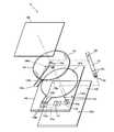
図3は充電器10のコイルユニット12を模式的に示す分解斜視図である。なお、図3は、図1においてコイルユニット12が携帯電話機20のコイルユニット22と対向する伝送面とは逆側の非伝送面側から、コイルユニット12を見た図である。2. Coil Unit on Charger (Primary) Side FIG. 3 is an exploded perspective view schematically showing the
コイルユニット12は、コイル線131を巻回して形成される平面状コイル130と、平面状コイル130の磁路を形成する磁性シート160とを有する。 The
さらにこのコイルユニット12は、平面状コイル130が配置される面内にて、平面状コイル130と平行に配置されるフレキシブル基板181と、フレキシブル基板181に搭載された温度検出素子例えばサーミスタ180とを有する。 Further, the
本実施形態のコイルユニット12は、平面状コイル130、磁性シート160及びフレキシブル基板181という薄型構成要素を積層しているので、コイルユニット12の薄型化を維持できる。また、平面状コイル130が配置される面内に温度検出素子例えばサーミスタ180が配置されるので、図2に示す一次コイルL1(130)と二次コイルL2間に異物が混入した時の温度上昇をサーミスタ180にて検出することができる。 Since the
平面状コイル130は、本実施形態では、中心に空芯部130aを有し、コイル線131が平面上でスパイラル状に巻回された空芯コイルである。この場合、フレキシブル基板181に搭載されたサーミスタ180は、平面状コイル130の空芯部130aに位置するように配置されている。このサーミスタ180及びフレキシブル基板181の詳細については後述する。 In the present embodiment, the
本実施形態では、平面状コイル130の一面を伝送面とし他面を非伝送面としたとき、磁性シート160は平面状コイル130の非伝送面側に配置される。このとき、フレキシブル基板181は、コイル線131と磁性シート160との間、つまり平面状コイル130の非伝送面と磁性シート160との間に配置することができる。こうすると、平面状コイル130の伝送面側にフレキシブル基板181が存在しないので、図2に示す一次コイルL1(130)と二次コイルL2間の伝送間距離を短縮でき、伝送効率が向上する。 In the present embodiment, when one surface of the
コイルユニット12は、配線基板140をさらに有することができる。この配線基板140は、コイルユニット12の保形性を維持するのに好ましいことと、平面状コイル130やフレキシブル基板181を電気的に中継接続することができる点で好ましい。 The
本実施形態では、配線基板140にはコイル収容部140aが形成され、このコイル収容部140aは、例えば表裏面に貫通するコイル収容穴にて形成されている。このコイル収容穴140aに平面状コイル130が収容される。これにより、平面状コイル130のスパイラル巻回部分の厚さの全部または一部は、配線基板140のコイル収容穴140aにて吸収され、コイルユニット12の総厚を薄くできる。また、平面状コイル130の伝送面側が配線基板140のコイル収容穴140aを介して露出するので、図2に示す一次コイルL1(130)と二次コイルL2間の伝送間距離を短縮でき、伝送効率が向上する。 In the present embodiment, a
なお、配線基板140の伝送面側には、平面状コイル130および配線基板140を保護するための保護シート150を設けることができる。 A
以下、各構成要素についてさらに具体的に説明する。 Hereinafter, each component will be described more specifically.
平面状コイル130は、平面的なコイルであれば特に限定されないが、たとえば、単芯または多芯の被覆コイル線を平面上で巻回した空芯コイルを適用することができる。本実施形態で10数本の多芯のコイル線を採用している。 The
平面状コイル130は、上述したように、配線基板140に設けられたコイル収容部140aに収容されている。このようにコイル収容部140aに平面状コイル130を収容することで、上述したコイルユニット12の薄型化に寄与できる他、平面状コイル130の伝送面をその周囲の面と面一にし易い。事実、本実施形態では保護シート150には凹凸は生じない。また、コイル収容穴140aは、平面状コイル130の外形に対応した形状を有する。これにより、平面状コイル130をコイル収容穴140aに収容しさえすれば、平面状コイル130を配線基板140に位置決めすることができるため、位置決めが容易となる。 As described above, the
平面状コイル130は、コイル内端を引き出すコイル内端引き出し線130bと、コイル外端を引き出すコイル外端引き出し線130cとを有する。コイル内端引き出し線130bは、図3で示すように、平面状コイル130の非伝送面側から引き出されることが好ましい。非伝送面側からコイル内端引き出し線130bを引き出すことで、伝送面がコイル内端引き出し線130bによって凸部が生じるのを防ぐことができるため、伝送面を面一にすることができると共に、伝送効率を向上させることができる。 The
配線基板140には、コイル収容穴140aと連続して引き出し線収容穴140hが設けられている。引き出し線収容穴140hは、平面状コイル130のコイル内端引き出し線130bおよびコイル外端引き出し線130cを収容するためのものである。引き出し線収容穴140hがあることで、引き出し線130b、130cがそこに収容されているため、その領域において引き出し線130b、130cの厚み分だけ薄型化をすることができる。また、引き出し線130b、130cは、引き出し線収容部140hにて比較的緩やかに屈曲されて配線基板140に乗り上げるため、断線が少なくなる。 The
コイル内端引き出し線130bおよびコイル外端引き出し線130cは、コンタクト電極(コイル接続端子)140bまで引き出され、半田付けにより配線電極140bと電気的に接続されている。コンタクト電極140bは、配線基板140の非伝送面側(図3では手前側)に設けられている。 The coil inner
図3に示すように、配線基板140には、外部接続端子141、142が設けられており、一方の外部接続端子141は、配線基板140の伝送面側に設けられた配線141aで一方のコンタクト電極140bに接続され、他方の外部接続端子142は、配線基板140の伝送面側に設けられた配線142aで他方のコンタクト電極140bに接続されている。配線基板140は、保護シート150と位置決めするための複数例えば2つの位置決め孔140eが設けられている。 As shown in FIG. 3,
保護シート150は、少なくとも平面状コイル130を保護するためのシートであるが、本実施形態では配線基板140及び平面状コイル130の伝送面側全体を覆っている。保護シート150は第一義的には絶縁性のものであれば特に限定されない。保護シート150は、図3に示すように、配線基板140の位置決め孔140eと対応した位置に、位置決め孔150bが設けられている。この位置決め孔140e、150bにより、配線基板140と保護シート150との間で位置決めしやすい。また、本実施形態では、保護シート150は配線基板140に一致した外形であるが、これに限定されない。保護シート150の形状(面積)は、コイルユニットの伝送面側が接触する外装ケースの内部形状(面積)と接触面積が最大になるように形成することができる。こうすると、放熱効果はより高まる。 The
平面状コイル130の内側端子は、非伝送面側から引き出してある。このようにすることで、伝送面が面一になることによって、平面状コイル130と保護シート(放熱シート)150の密着性が高まり、接触熱抵抗が低減されて放熱しやすくなるという効果を奏することができる。 The inner terminal of the
磁性シート160は、平面状コイル130の非伝送面側に貼り付けられている。磁性シート160は、平面状コイル130からの磁束を受ける働きをし、平面状コイル130のインダクタンスを上げるという基本機能を有する。磁性シートの材質としては、軟磁性材、フェライト軟磁性材、金属軟磁性材、等々種々の磁性材料を用いることができる。 The
充電器10側の磁性シート160は、比較的柔軟性の高い材質を使用することができる。このため、一次コイル130のコイル内端引き出し線130bやフレキシブル基板181が、一次コイル130の非伝送面側にて突出しても、磁性シート160をその突出部に倣って変形させることができる。従って、一次コイル130と磁性シート160との間に、コイル内端引き出し線130bやフレキシブル基板181の厚みを吸収するスペーサを配置する必要はない。ただし、フレキシブル基板181は極薄いので、磁性シート160の変形はほとんど生じない。 The
3.一次コイルの温度検出素子
図1に示したような電磁誘導作用を利用した無接点電力伝送システムにおいて、電力伝送時にコイルユニット12とコイルユニット22との間に金属製の異物が存在すると、その異物に渦電流が生じて発熱し、異物および一次コイル130が過加熱状態となることがある。また、異物が存在しなくても、何らかの理由によりコイル130が過加熱状態となることもある。3. Temperature detection element of primary coil In the non-contact power transmission system using the electromagnetic induction action as shown in FIG. An eddy current may be generated and heat may be generated, and the foreign matter and the
そこで本実施形態では、平面状コイル130により磁力線が形成される領域(磁力線形成領域)に温度検出素子(温度検知センサ)の一例であるサーミスタ180を配置している。本実施形態では特に、平面状コイル130の空芯部130aにサーミスタ180を配置し、平面状コイル130およびその周辺の温度を監視する。本実施形態では、空芯部130aは磁束密度が特に大きく、この空芯部130aに異物が混入した時に、異物に生ずる渦電流による温度上昇が最も激しく、発熱も大きいからである。このようにすると、空芯部130a近くに異物が混入したことを、サーミスタ180により確実に検知できる。 Therefore, in the present embodiment, the
そして、サーミスタ180による検知温度が一定温度以上となったとき、あるいは周囲温度とサーミスタ検知温度が一定値以上となったとき、あるいは温度上昇速度が一定値以上となったときに、充電器10側の平面状コイル130の駆動を停止することができる。 When the temperature detected by the
サーミスタ180は、フレキシブル配線基板181を用いて平面状コイル130の空芯部130aに配置される。フレキシブル配線基板181は、その先端にサーミスタ180が設けられ、他端に電極182が設けられている。フレキシブル配線基板181は、平面状コイル130と磁性シート160との間にあって平面状コイル130の非伝送面側において、平面状コイル130の空芯部130aより放射方向(半径方向)に沿って配置される。これによって、フレキシブル基板181の一端側に搭載されたサーミスタ180が、平面状コイル130の空芯部130aに配置される。フレキシブル配線基板181の電極182は、配線基板140の電極143と接続される。 The
4.一次コイルユニットと制御ユニット
図4は、コイルユニット12と制御ユニット190とを電気的に接続した形態を示している。このコイルユニット12と制御ユニット190とで送電装置が構成される。図4に示すコイルユニット12は、コイル内端・外端引き出し線130b,130cやフレキシブル基板181等の配置が図3とは異なるが、基本的構造は図3と同じである。4). Primary Coil Unit and Control Unit FIG. 4 shows a form in which the
図4に示すコイルユニット12では、基板140に収容された平面状コイル130の非伝送面側の磁性シート160は、基板140の表面より突出する平面状コイル130に沿って変形した第1の変形部161と、コイル内端引き出し線130bに沿って変形した第2の変形部162を有する。フレキシブル基板181は極薄いので、磁性シート160はほとんど変形しないでフレキシブル基板181の厚みを吸収できる。 In the
図4に示す制御ユニット190は、コイルユニット12とは別体で形成されている。コイルユニット12の基板140には外部接続端子141,142(図3)に接続される第1のコネクタ145が搭載され、制御ユニット190の基板191には第2のコネクタ192が搭載されている。第1,第2のコネクタ145,192同士を電気的に接続することで、コイルユニット12と制御ユニット190とが電気的に接続される。 The
制御ユニット190は、コイルユニット12を駆動するための各種回路が搭載されている。例えば、制御ユニット190は、一次コイル130に通電して無接点電力伝送を行うための送電回路を含んでいる。この送電回路には送電制御部が配置される。送電制御部は、コイルユニット12のサーミスタ180からの信号が入力され、異常温度が検出された時に一次コイル130への通電を遮断できる。 Various circuits for driving the
5.伝送装置
図5は、図3に示すコイルユニット12と図4に示す制御ユニット190とを含む伝送装置の概略ブロック図である。図5において、この伝送装置は、制御ユニット190が送電部200、送電制御部210及び異常温度上昇検出部220を含んでいる。5. Transmission Device FIG. 5 is a schematic block diagram of a transmission device including the
送電部200は、電力伝送時には所定周波数の交流電圧を生成し、データ転送時にはデータに応じて周波数が異なる交流電圧を生成して、一次コイルL1(130)に供給する。この送電部200は、一次コイルL1の一端を駆動する第1の送電ドライバと、一次コイルL1の他端を駆動する第2の送電ドライバと、一次コイルL1と共に共振回路を構成する少なくとも1つのコンデンサを含むことができる。そして、送電部200が含む第1、第2の送電ドライバの各々は、例えばパワーMOSトランジスタにより構成されるインバータ回路(バッファ回路)であり、送電制御部210により制御される。送電制御部210での制御は、異常温度上昇検出部220からの信号に基づいて、一次コイルL1への通電を停止して送電を停止する制御を含んでいる。 The
図6は図5に示す異常温度上昇検出部220の一例を示すブロック図である。図6において、高電位線221と低電位線222との間には、サーミスタ180を含む分圧回路223が設けられている。この分圧回路223で分圧されたアナログ電圧はアナログ−デジタル(A/D)変換器224に入力される。A/D変換器224は、分圧された電圧をデジタル信号に変換する。遅延回路225は、A/D変換器224からのデジタル信号を遅延させる。減算器226は、遅延回路225からの第1の時刻での信号とA/D変換器224からの第2の時刻での信号との間の差分を演算する。 FIG. 6 is a block diagram showing an example of the abnormal temperature
本実施形態では、遅延回路225からの第1の時刻での信号(第1の電圧)からA/D変換器224からの第2の時刻での信号(第2の電圧)を減算する。減算器226の出力がプラスであれば、サーミスタ180は温度上昇中の温度を検出したことを意味し、減算器226の出力がマイナスであれば、サーミスタ180は温度降下した温度を検出したことを意味する。 In the present embodiment, the signal (second voltage) at the second time from the A /
比較器227は、基準値Refと減算器226の出力とを比較する。基準値Refは、遅延回路225にて遅延された時間(単位時間)あたりの異常温度上昇時の値がセットされている。よって、比較器226での比較出力がプラス(温度上昇中)であって、かつ、単位時間当たりの温度上昇値が基準値Ref以上であれば、比較器227より例えばHが出力され、それ以外であればLが出力される。 The
つまり、図6に示す異常温度上昇検出部220は、サーミスタ180の可変抵抗値によって変化する第1の時刻の電圧である第1の電圧と第2の時刻の電圧である第2の電圧に基づいて、異常温度上昇を検出することができる。 That is, the abnormal temperature
送電制御部210は、異常温度上昇検出部220の出力、つまり比較器227の出力が入力され、比較器227の出力がHであれば送電を停止制御し、比較器227の出力がLであれば送電を継続する。 The power
図7は、送電開始時からの温度上昇カーブを示す特性図である。図7において、正常時には通電による一次コイルL1等の発熱によりサーミスタ180での検出温度は、図7中のT1にて変化する。つまり、送電開始により温度が上昇し、時刻t1にて温度上昇率が最大となり、その後温度上昇率は低下し、飽和温度に達することで温度上昇率は0となる。 FIG. 7 is a characteristic diagram showing a temperature rise curve from the start of power transmission. In FIG. 7, the temperature detected by the
図7において、一次・二次コイルL1,L2間であって一次コイルL1の空芯部130aに異物が存在した時の温度上昇カーブをT2とし、空芯部130aより外れた位置に異物が存在した時間の温度上昇カーブをT3とする。上昇カーブT2は上昇カーブT3よりも送電開始後の温度上昇率が大きいとしても、異常時のカーブT2,T3はともに、正常時のカーブT1よりも、送電開始後の温度上昇率は大きい。 In FIG. 7, the temperature rise curve is T2 between the primary and secondary coils L1 and L2 and when the foreign matter is present in the
よって、図6の比較器227に設定される基準値Refとしては、正常時の上昇カーブT1と異常時の上昇カーブT3との間に所定のマージンMが確保される値をしきい値とすれば、この閾値よりも高い温度上昇率が発生した時を異常と判定できる。 Therefore, as the reference value Ref set in the
本実施形態では、例えばコイル電流が2mA時に0.2秒毎にサーミスタ180にて温度検出し、単位時間例えば10秒前(第1の時刻)での第1の温度と、現在(第2の時刻)での第2の温度との間の温度差を、閾値と比較することで、異常時に送電停止することができる。特に、温度の立ち上がり速度を見ているので、温度がある絶対値(危険温度)に達する前に異常して、送電を停止制御することができる。 In the present embodiment, for example, when the coil current is 2 mA, the temperature is detected by the
ただし、温度上昇率及び正常−異常時のマージンMは、一次側コイルユニット12の周囲の部材、例えば一次側筐体の材質、厚さ、形状またはコイルユニット12と筐体の間の距離などの放熱環境で異なるので、比較器227の基準値は、製品毎に調整し、あるいは出荷時に調整することが好ましい。 However, the temperature rise rate and the normal-abnormal margin M are the members around the
図8は、図5に示す異常温度上昇検出部220の他の一例を示すブロック図である。図8に示す異常温度上昇検出部220は、図6に示すA/D変換器224を抵抗値−周波数(R/F)変換器230と周波数カウンタ231に置き換えたものである。R/F変換器230は、サーミスタ180の抵抗値を周波数に変換するもので、サーミスタ180の抵抗と共にRC回路を形成している。図9は、R/F変換器230の出力信号を示しており、RC回路の時定数に基づいて変化する信号を、所定の閾値Vrefと比較して矩形波に変換している。周波数カウンタ231は、図9に示すように、R/F変換器230からの出力信号をクロック信号で計数するものである。 FIG. 8 is a block diagram showing another example of the abnormal temperature
ここで、サーミスタ180が例えば高温時に抵抗値が小さくなる負特性であれば、高温時にはRC回路の時定数は小さくなり高周波数となる一方で、低温時にはRC回路の時定数が大きくなり低周波数となる。このように、周波数が温度と相関を有するため、図6にて温度と相関のある電圧値に基づいて温度時上昇率を検出した場合と同様にして、異常時の温度上昇を検出できる。つまり、図8の異常温度上昇検出部220は、サーミスタ180の可変抵抗値によって変化する第1の時刻の周波数である第1の周波数と第2の時刻の周波数である第2の周波数を比較した結果に基づいて、異常温度上昇を検出することができる。 Here, if the
6.変形例
なお、上記のように本実施形態について詳細に説明したが、本発明の新規事項および効果から実体的に逸脱しない多くの変形が可能であることは当業者には容易に理解できるものである。従って、このような変形例はすべて本発明の範囲に含まれるものとする。例えば、明細書又は図面において、少なくとも一度、より広義または同義な異なる用語と共に記載された用語は、明細書又は図面のいかなる箇所においても、その異なる用語に置き換えることができる。6). Although the present embodiment has been described in detail as described above, those skilled in the art can easily understand that many modifications can be made without departing from the novel matters and effects of the present invention. is there. Accordingly, all such modifications are intended to be included in the scope of the present invention. For example, a term described at least once together with a different term having a broader meaning or the same meaning in the specification or the drawings can be replaced with the different term in any part of the specification or the drawings.
上述した実施形態では、図1に示す電子機器のうち、特に小型・軽量化が求められる携帯電話機20側のコイルユニット12に適用した例であったが、充電器10のコイルユニット22に適用しても良い。 In the above-described embodiment, the electronic device illustrated in FIG. 1 is an example applied to the
また、本実施の形態は、電力伝送や信号伝送を行うすべての電子機器に適用可能であり、たとえば、腕時計、電動歯ブラシ、電動ひげ剃り、コードレス電話、パーソナルハンディフォン、モバイルパソコン、PDA(Personal Digital Assistants)、電動自転車などの二次電池を備える被充電機器と充電機器とに適用可能である。 The present embodiment can be applied to all electronic devices that perform power transmission and signal transmission. For example, wristwatches, electric toothbrushes, electric shavings, cordless phones, personal handyphones, mobile personal computers, PDAs (Personal Digital) Assistants), and can be applied to rechargeable devices and rechargeable devices including secondary batteries such as electric bicycles.
さらに、本発明が適用されるコイルユニットは、スパイラル状に巻回した空芯の平面状コイルに限らず、他の種々のコイルを使用しても良い。 Furthermore, the coil unit to which the present invention is applied is not limited to an air-core planar coil wound in a spiral shape, and other various coils may be used.
図10は、上述した実施形態とは異なるタイプのコイルユニット300を示している。このコイルユニット300は、例えば平板状の磁性体コア310の周囲にコイル線320を巻回したコイル330を有する。このコイルユニット300のコイル線320に交流電流を流すと、磁性体コア310に磁路が形成されると共に、この磁性体コア310と平行に磁束線が形成される。このコイルユニット300を一次コイルL1として用いても、二次コイルL2との磁気結合により無接点電力伝送が可能である。 FIG. 10 shows a
つまり、本発明は、コイルの一面に磁性体を有するものに限らず、磁性体をコアとして使用するものにも適用できる。コイルとそのコイルの磁路を形成する磁性体との組み合わせは、上述したものに限らず、他の種々の形状のコイル及び磁性体を組み合わせても良く、必ずしも平面的な薄型コイルユニットでなくてもよい。一次・二次コイルL1,L2間に介在した異物の発熱に伴う温度上昇率に基づいて異常検出できるものであれば、コイルの種別は問わない。 That is, the present invention is not limited to one having a magnetic body on one surface of the coil, but can be applied to one using a magnetic body as a core. The combination of the coil and the magnetic body forming the magnetic path of the coil is not limited to the above-described one, and other various shapes of coils and magnetic bodies may be combined, and not necessarily a flat thin coil unit. Also good. The type of the coil is not limited as long as it can detect an abnormality based on the rate of temperature rise caused by the heat generated by the foreign matter interposed between the primary and secondary coils L1 and L2.
10 充電器(電子機器)、12 一次コイルユニット(コイルユニット)、
20 携帯電話機(電子機器)、22 二次コイルユニット、
130 一次コイル(平面状コイル)、130a 空芯部、
130b コイル内端引き出し線、130c コイル外端引き出し線、
131 コイル線、140 基板、140a コイル収容部、150 保護シート、
160 磁性シート、180 温度検出素子(可変抵抗素子、サーミスタ)、
181 フレキシブル基板、183 位置決め孔、190 制御ユニット、
191 基板、200 送電部、210 送電制御部、220 異常温度上昇検出部、
221 高電位線、222 低電位線、223 分圧回路、224 A/D変換器、
225 遅延回路、226 減算器、227 比較器、
230 抵抗値−周波数(R/F)変換回路、231 周波数カウンタ10 charger (electronic device), 12 primary coil unit (coil unit),
20 mobile phone (electronic device), 22 secondary coil unit,
130 primary coil (planar coil), 130a air core,
130b Coil inner end lead wire, 130c Coil outer end lead wire,
131 coil wire, 140 substrate, 140a coil housing portion, 150 protective sheet,
160 magnetic sheet, 180 temperature detection element (variable resistance element, thermistor),
181 flexible substrate, 183 positioning hole, 190 control unit,
191 substrate, 200 power transmission unit, 210 power transmission control unit, 220 abnormal temperature rise detection unit,
221 high potential line, 222 low potential line, 223 voltage dividing circuit, 224 A / D converter,
225 delay circuit, 226 subtractor, 227 comparator,
230 Resistance Value-Frequency (R / F) Conversion Circuit, 231 Frequency Counter
Claims (7)
Translated fromJapanese前記一次コイルに交流信号を供給する送電部と、
前記一次コイルの磁力線形成領域に配置される温度検出素子と、
前記温度検出素子にて検出される第1の時刻の温度である第1の温度と第2の時刻の温度である第2の温度とに基づいて、異常温度上昇を検出する異常温度上昇検出部と、
前記送電部を送電制御し、前記異常温度上昇検出部にて前記異常温度上昇が検出された時に前記一次コイルからの送電を停止制御する送電制御部と、
を有することを特徴とする送電装置。In a power transmission device that includes a primary coil, electromagnetically couples the primary coil to a secondary coil of a power reception device, and supplies power to a load of the power reception device.
A power transmission unit for supplying an AC signal to the primary coil;
A temperature detecting element disposed in a magnetic force line forming region of the primary coil;
An abnormal temperature rise detection unit that detects an abnormal temperature rise based on a first temperature that is a temperature at a first time detected by the temperature detection element and a second temperature that is a temperature at a second time. When,
A power transmission control unit that performs power transmission control on the power transmission unit, and controls to stop power transmission from the primary coil when the abnormal temperature increase detection unit detects the abnormal temperature increase;
A power transmission device comprising:
前記温度検出素子は、温度によって抵抗値が変化する可変抵抗素子であることを特徴とする送電装置。In claim 1,
The power transmission device, wherein the temperature detection element is a variable resistance element whose resistance value varies with temperature.
前記異常温度上昇検出部は、前記可変抵抗素子によって変化する前記第1の時刻の電圧である第1の電圧と前記第2の時刻の電圧である第2の電圧に基づいて、前記異常温度上昇を検出することを特徴とする送電装置。In claim 2,
The abnormal temperature increase detection unit is configured to detect the abnormal temperature increase based on a first voltage that is a voltage at the first time and a second voltage that is a voltage at the second time, which are changed by the variable resistance element. A power transmission device characterized by detecting
前記異常温度上昇検出部は、前記可変抵抗素子の可変抵抗値を周波数変換する抵抗値−周波数変換回路を含み、前記可変抵抗値によって変化する前記第1の時刻の周波数である第1の周波数と前記第2の時刻の周波数である第2の周波数を比較した結果に基づいて、前記異常温度上昇を検出することを特徴とする送電装置。In claim 2,
The abnormal temperature rise detection unit includes a resistance value-frequency conversion circuit that frequency-converts a variable resistance value of the variable resistance element, and a first frequency that is a frequency at the first time that varies according to the variable resistance value; The power transmission device that detects the abnormal temperature rise based on a result of comparing a second frequency that is a frequency at the second time.
前記異常温度上昇検出部は、前記温度検出素子にて検出される前記第1の温度と前記第2の温度との差分結果と、基準値とを比較する比較器を含み、前記基準値は調整可能であることを特徴とする送電装置。In claim 3 or 4,
The abnormal temperature rise detection unit includes a comparator that compares a difference result between the first temperature and the second temperature detected by the temperature detection element with a reference value, and the reference value is adjusted. A power transmission device characterized in that it is possible.
前記一次コイルは空芯部を有する空芯コイルであり、
前記温度検出素子は前記空芯部に配置されることを特徴とする送電装置。In any one of Claims 1 thru | or 5,
The primary coil is an air core coil having an air core portion,
The power transmission device, wherein the temperature detection element is disposed in the air core part.
Priority Applications (3)
| Application Number | Priority Date | Filing Date | Title |
|---|---|---|---|
| JP2008122270AJP2009273260A (en) | 2008-05-08 | 2008-05-08 | Non-contact power transmission apparatus, power transmission apparatus and electronic apparatus using the same |
| US12/434,370US20090278523A1 (en) | 2008-05-08 | 2009-05-01 | Non-contact power transmission device, power transmission device and electronic apparatus using the same |
| CN200910136420.1ACN101577446B (en) | 2008-05-08 | 2009-05-07 | Non-contact power transmission device, power transmission device and electronic apparatus using the same |
Applications Claiming Priority (1)
| Application Number | Priority Date | Filing Date | Title |
|---|---|---|---|
| JP2008122270AJP2009273260A (en) | 2008-05-08 | 2008-05-08 | Non-contact power transmission apparatus, power transmission apparatus and electronic apparatus using the same |
Publications (1)
| Publication Number | Publication Date |
|---|---|
| JP2009273260Atrue JP2009273260A (en) | 2009-11-19 |
Family
ID=41266318
Family Applications (1)
| Application Number | Title | Priority Date | Filing Date |
|---|---|---|---|
| JP2008122270APendingJP2009273260A (en) | 2008-05-08 | 2008-05-08 | Non-contact power transmission apparatus, power transmission apparatus and electronic apparatus using the same |
Country Status (3)
| Country | Link |
|---|---|
| US (1) | US20090278523A1 (en) |
| JP (1) | JP2009273260A (en) |
| CN (1) | CN101577446B (en) |
Cited By (16)
| Publication number | Priority date | Publication date | Assignee | Title |
|---|---|---|---|---|
| JP2011211854A (en)* | 2010-03-30 | 2011-10-20 | Nippon Soken Inc | Voltage detector, abnormality detection device, non-contact power transmitting device, non-contact power receiving device, non-contact power supply system, and vehicle |
| JP2012182258A (en)* | 2011-02-28 | 2012-09-20 | Mitsubishi Materials Corp | Non-contact power supply device with temperature sensor |
| JP2012249406A (en)* | 2011-05-27 | 2012-12-13 | Nissan Motor Co Ltd | Non-contact power supply device |
| WO2012176569A1 (en)* | 2011-06-21 | 2012-12-27 | パナソニック 株式会社 | Contactless power transmission system |
| WO2013011908A1 (en)* | 2011-07-20 | 2013-01-24 | 三洋電機株式会社 | Battery pack |
| JP2013543719A (en)* | 2010-10-06 | 2013-12-05 | ワイトリシティ コーポレイション | Vehicle charger safety system and method |
| JP2014007863A (en)* | 2012-06-25 | 2014-01-16 | Canon Inc | Power supply device, control method, and program |
| KR101450115B1 (en) | 2013-06-17 | 2014-10-14 | (주)엠에이피테크 | Power reception coil module for wireless charging |
| JP2015029114A (en)* | 2014-09-02 | 2015-02-12 | 株式会社村田製作所 | Coil module and electronic apparatus having the same |
| US9404954B2 (en) | 2012-10-19 | 2016-08-02 | Witricity Corporation | Foreign object detection in wireless energy transfer systems |
| JP2016149937A (en)* | 2012-06-22 | 2016-08-18 | ソニー株式会社 | Power transmission device, power transmission method, power receiving device, power receiving method, and wireless power supply system |
| US9442172B2 (en) | 2011-09-09 | 2016-09-13 | Witricity Corporation | Foreign object detection in wireless energy transfer systems |
| KR20160118350A (en)* | 2014-03-26 | 2016-10-11 | 애플 인크. | Temperature management for inductive charging systems |
| JP2017034733A (en)* | 2015-07-28 | 2017-02-09 | トヨタ自動車株式会社 | Contactless charging system |
| JP2019097389A (en)* | 2017-07-27 | 2019-06-20 | ソニー株式会社 | Power transmission device, power transmission method, power reception device, and power reception method |
| US11309746B2 (en) | 2012-06-22 | 2022-04-19 | Sony Group Corporation | Wireless power transfer device with foreign object detection, system, and method for performing the same |
Families Citing this family (25)
| Publication number | Priority date | Publication date | Assignee | Title |
|---|---|---|---|---|
| JP5526833B2 (en)* | 2010-02-05 | 2014-06-18 | ソニー株式会社 | Wireless power transmission device |
| WO2011125632A1 (en)* | 2010-03-31 | 2011-10-13 | 本田技研工業株式会社 | Contactless charging system |
| DE102010020122B4 (en)* | 2010-05-10 | 2021-07-15 | Sew-Eurodrive Gmbh & Co Kg | Arrangement for contactless energy transfer |
| DE102010020125B4 (en)* | 2010-05-10 | 2021-07-15 | Sew-Eurodrive Gmbh & Co Kg | Arrangement for contactless energy transfer |
| DE102010026780A1 (en)* | 2010-07-09 | 2012-01-12 | Audi Ag | Measuring a temperature during contactless transmission of energy |
| JP5605153B2 (en)* | 2010-10-15 | 2014-10-15 | ソニー株式会社 | Power supply device, power supply method, and power supply system |
| JP2012186472A (en)* | 2011-02-19 | 2012-09-27 | Lequio Power Technology Corp | Power supply device and power reception/supply device |
| WO2013125072A1 (en)* | 2012-02-20 | 2013-08-29 | レキオ・パワー・テクノロジー株式会社 | Power supply device, power reception device, and power supply/reception device |
| US20120274148A1 (en)* | 2011-04-27 | 2012-11-01 | Samsung Electro-Mechanics Co., Ltd. | Contactless power transmission device and electronic device having the same |
| DE102011076186A1 (en)* | 2011-05-20 | 2012-11-22 | Siemens Aktiengesellschaft | Arrangement and method for eliminating a disturbance of a wireless energy transmission |
| US9417199B2 (en) | 2012-01-17 | 2016-08-16 | Triune Systems, LLC | Method and system of wireless power transfer foreign object detection |
| EP2621050B1 (en)* | 2012-01-27 | 2015-04-08 | Braun GmbH | Inductive Charger for Hand-Held Appliances |
| JP5244250B1 (en)* | 2012-03-28 | 2013-07-24 | パナソニック株式会社 | Power supply device |
| FR2998412B1 (en)* | 2012-11-19 | 2014-12-26 | Continental Automotive France | METHOD FOR SEARCHING FOR THE PRESENCE OF A PARASITE OBJECT FOR A MAGNETIC INDUCTION POWER TRANSMITTING UNIT |
| JP5880455B2 (en)* | 2013-01-16 | 2016-03-09 | ソニー株式会社 | Power receiving device, non-contact power transmission system, and power receiving voltage control method |
| JP6052397B2 (en)* | 2013-03-29 | 2016-12-27 | 日産自動車株式会社 | Power supply device and power transmission unit of power supply device |
| CN105137489B (en)* | 2014-06-09 | 2020-03-17 | 中兴通讯股份有限公司 | Foreign matter detection method and device, and wireless charging control method and device |
| USD785564S1 (en)* | 2016-03-17 | 2017-05-02 | Samsung Electronics Co., Ltd. | Wireless charger for electronic device |
| DE112017007722T5 (en)* | 2017-08-01 | 2020-04-02 | Ford Global Technologies, Llc | ACTIVATING A WIRELESS CHARGER |
| EP3692555B1 (en)* | 2017-10-06 | 2021-04-21 | Sew-Eurodrive GmbH & Co. KG | System for non-contact transmission of electrical energy to a mobile part |
| US20190181693A1 (en)* | 2017-12-08 | 2019-06-13 | Toshiba Tec Kabushiki Kaisha | Non-contact power receiving device and non-contact power transmitting device |
| US10658878B2 (en)* | 2018-08-31 | 2020-05-19 | Apple Inc. | Wireless charging system with temperature sensor array |
| US10505403B1 (en) | 2018-08-31 | 2019-12-10 | Apple Inc. | Wireless charging system with temperature sensing |
| CN110165636A (en)* | 2019-04-28 | 2019-08-23 | 华为技术有限公司 | A kind of excess temperature protection method, device and electronic equipment |
| KR20230056262A (en)* | 2021-10-20 | 2023-04-27 | 삼성전자주식회사 | Wireless power transmission apparatus |
Citations (4)
| Publication number | Priority date | Publication date | Assignee | Title |
|---|---|---|---|---|
| JPH10179452A (en)* | 1996-10-28 | 1998-07-07 | Matsushita Electric Works Ltd | Toilet stool with seat |
| JP2003153457A (en)* | 2001-11-09 | 2003-05-23 | Denso Corp | Noncontact charger |
| JP2004208383A (en)* | 2002-12-25 | 2004-07-22 | Aichi Electric Co Ltd | Non-contact power supply |
| JP2007324532A (en)* | 2006-06-05 | 2007-12-13 | Meleagros Corp | Power transmission method, method for selecting and using coil of power transmission device |
Family Cites Families (4)
| Publication number | Priority date | Publication date | Assignee | Title |
|---|---|---|---|---|
| JP3545585B2 (en)* | 1998-01-19 | 2004-07-21 | 矢崎総業株式会社 | Temperature voltage detection unit |
| US6501364B1 (en)* | 2001-06-15 | 2002-12-31 | City University Of Hong Kong | Planar printed-circuit-board transformers with effective electromagnetic interference (EMI) shielding |
| KR100836634B1 (en)* | 2006-10-24 | 2008-06-10 | 주식회사 한림포스텍 | Portable terminal using a contactless charger, a battery pack for charging and a contactless charger for wireless data communication and power transmission |
| JP4508266B2 (en)* | 2008-05-12 | 2010-07-21 | セイコーエプソン株式会社 | Coil unit and electronic device using the same |
- 2008
- 2008-05-08JPJP2008122270Apatent/JP2009273260A/enactivePending
- 2009
- 2009-05-01USUS12/434,370patent/US20090278523A1/ennot_activeAbandoned
- 2009-05-07CNCN200910136420.1Apatent/CN101577446B/ennot_activeExpired - Fee Related
Patent Citations (4)
| Publication number | Priority date | Publication date | Assignee | Title |
|---|---|---|---|---|
| JPH10179452A (en)* | 1996-10-28 | 1998-07-07 | Matsushita Electric Works Ltd | Toilet stool with seat |
| JP2003153457A (en)* | 2001-11-09 | 2003-05-23 | Denso Corp | Noncontact charger |
| JP2004208383A (en)* | 2002-12-25 | 2004-07-22 | Aichi Electric Co Ltd | Non-contact power supply |
| JP2007324532A (en)* | 2006-06-05 | 2007-12-13 | Meleagros Corp | Power transmission method, method for selecting and using coil of power transmission device |
Cited By (29)
| Publication number | Priority date | Publication date | Assignee | Title |
|---|---|---|---|---|
| JP2011211854A (en)* | 2010-03-30 | 2011-10-20 | Nippon Soken Inc | Voltage detector, abnormality detection device, non-contact power transmitting device, non-contact power receiving device, non-contact power supply system, and vehicle |
| JP2013543719A (en)* | 2010-10-06 | 2013-12-05 | ワイトリシティ コーポレイション | Vehicle charger safety system and method |
| JP2012182258A (en)* | 2011-02-28 | 2012-09-20 | Mitsubishi Materials Corp | Non-contact power supply device with temperature sensor |
| JP2012249406A (en)* | 2011-05-27 | 2012-12-13 | Nissan Motor Co Ltd | Non-contact power supply device |
| WO2012176569A1 (en)* | 2011-06-21 | 2012-12-27 | パナソニック 株式会社 | Contactless power transmission system |
| JP2013005682A (en)* | 2011-06-21 | 2013-01-07 | Panasonic Corp | Non-contact power transmission system |
| WO2013011908A1 (en)* | 2011-07-20 | 2013-01-24 | 三洋電機株式会社 | Battery pack |
| US9442172B2 (en) | 2011-09-09 | 2016-09-13 | Witricity Corporation | Foreign object detection in wireless energy transfer systems |
| US10778047B2 (en) | 2011-09-09 | 2020-09-15 | Witricity Corporation | Foreign object detection in wireless energy transfer systems |
| US10027184B2 (en) | 2011-09-09 | 2018-07-17 | Witricity Corporation | Foreign object detection in wireless energy transfer systems |
| US11309746B2 (en) | 2012-06-22 | 2022-04-19 | Sony Group Corporation | Wireless power transfer device with foreign object detection, system, and method for performing the same |
| US10566849B2 (en) | 2012-06-22 | 2020-02-18 | Sony Corporation | Wireless power transfer device with foreign object detection, system, and method for performing the same |
| JP2016149937A (en)* | 2012-06-22 | 2016-08-18 | ソニー株式会社 | Power transmission device, power transmission method, power receiving device, power receiving method, and wireless power supply system |
| US9712001B2 (en) | 2012-06-22 | 2017-07-18 | Sony Corporation | Power reception apparatus, medium, and method for controlling electrical power supplied to a load of power reception apparatus |
| US10020693B2 (en) | 2012-06-22 | 2018-07-10 | Sony Corporation | Wireless power transfer device with foreign object detection, system, and method for performing the same |
| US9929605B2 (en) | 2012-06-22 | 2018-03-27 | Sony Corporation | Wireless power transfer device with foreign object detection, system, and method for performing the same |
| JP2014007863A (en)* | 2012-06-25 | 2014-01-16 | Canon Inc | Power supply device, control method, and program |
| US10211681B2 (en) | 2012-10-19 | 2019-02-19 | Witricity Corporation | Foreign object detection in wireless energy transfer systems |
| US9465064B2 (en) | 2012-10-19 | 2016-10-11 | Witricity Corporation | Foreign object detection in wireless energy transfer systems |
| US9404954B2 (en) | 2012-10-19 | 2016-08-02 | Witricity Corporation | Foreign object detection in wireless energy transfer systems |
| US10686337B2 (en) | 2012-10-19 | 2020-06-16 | Witricity Corporation | Foreign object detection in wireless energy transfer systems |
| KR101450115B1 (en) | 2013-06-17 | 2014-10-14 | (주)엠에이피테크 | Power reception coil module for wireless charging |
| JP2017511113A (en)* | 2014-03-26 | 2017-04-13 | アップル インコーポレイテッド | Temperature management for inductive charging systems |
| KR20160118350A (en)* | 2014-03-26 | 2016-10-11 | 애플 인크. | Temperature management for inductive charging systems |
| KR101951531B1 (en)* | 2014-03-26 | 2019-02-22 | 애플 인크. | Temperature management for inductive charging systems |
| US10320230B2 (en) | 2014-03-26 | 2019-06-11 | Apple Inc. | Temperature management for inductive charging systems |
| JP2015029114A (en)* | 2014-09-02 | 2015-02-12 | 株式会社村田製作所 | Coil module and electronic apparatus having the same |
| JP2017034733A (en)* | 2015-07-28 | 2017-02-09 | トヨタ自動車株式会社 | Contactless charging system |
| JP2019097389A (en)* | 2017-07-27 | 2019-06-20 | ソニー株式会社 | Power transmission device, power transmission method, power reception device, and power reception method |
Also Published As
| Publication number | Publication date |
|---|---|
| CN101577446B (en) | 2014-03-26 |
| CN101577446A (en) | 2009-11-11 |
| US20090278523A1 (en) | 2009-11-12 |
Similar Documents
| Publication | Publication Date | Title |
|---|---|---|
| CN101577446B (en) | Non-contact power transmission device, power transmission device and electronic apparatus using the same | |
| JP4508266B2 (en) | Coil unit and electronic device using the same | |
| US20250239769A1 (en) | Wireless Connector System | |
| JP4572953B2 (en) | Coil unit and electronic device using the same | |
| JP4281837B2 (en) | COIL UNIT, MANUFACTURING METHOD THEREOF, AND ELECTRONIC DEVICE | |
| KR101121481B1 (en) | Coil unit, manufacturing method thereof, and electronic machine | |
| US20080197711A1 (en) | Electronic device | |
| US9741488B2 (en) | Power transmission coil | |
| JP2010022098A (en) | Power conversion/transmission device and non-contact type charged device | |
| JP6617296B2 (en) | Built-in battery equipment |
Legal Events
| Date | Code | Title | Description |
|---|---|---|---|
| A977 | Report on retrieval | Free format text:JAPANESE INTERMEDIATE CODE: A971007 Effective date:20100412 | |
| A131 | Notification of reasons for refusal | Free format text:JAPANESE INTERMEDIATE CODE: A131 Effective date:20100420 | |
| A521 | Request for written amendment filed | Free format text:JAPANESE INTERMEDIATE CODE: A523 Effective date:20100618 | |
| A02 | Decision of refusal | Free format text:JAPANESE INTERMEDIATE CODE: A02 Effective date:20110208 |