JP2009266908A - Method for manufacturing semiconductor device and semiconductor device - Google Patents
Method for manufacturing semiconductor device and semiconductor deviceDownload PDFInfo
- Publication number
- JP2009266908A JP2009266908AJP2008112024AJP2008112024AJP2009266908AJP 2009266908 AJP2009266908 AJP 2009266908AJP 2008112024 AJP2008112024 AJP 2008112024AJP 2008112024 AJP2008112024 AJP 2008112024AJP 2009266908 AJP2009266908 AJP 2009266908A
- Authority
- JP
- Japan
- Prior art keywords
- inductor
- wiring
- region
- pattern
- semiconductor device
- Prior art date
- Legal status (The legal status is an assumption and is not a legal conclusion. Google has not performed a legal analysis and makes no representation as to the accuracy of the status listed.)
- Pending
Links
- 239000004065semiconductorSubstances0.000titleclaimsabstractdescription89
- 238000000034methodMethods0.000titleclaimsabstractdescription20
- 238000004519manufacturing processMethods0.000titleclaimsabstractdescription17
- 239000000758substrateSubstances0.000claimsabstractdescription76
- 230000002093peripheral effectEffects0.000claimsdescription11
- 238000010030laminatingMethods0.000claimsdescription2
- 239000010410layerSubstances0.000description90
- 239000010408filmSubstances0.000description39
- 230000008569processEffects0.000description12
- 238000009826distributionMethods0.000description11
- 230000004907fluxEffects0.000description8
- 229910052751metalInorganic materials0.000description6
- 239000002184metalSubstances0.000description6
- 238000004804windingMethods0.000description6
- 238000010586diagramMethods0.000description5
- 238000004891communicationMethods0.000description4
- 238000000151depositionMethods0.000description4
- 238000010897surface acoustic wave methodMethods0.000description3
- 238000007740vapor depositionMethods0.000description3
- RYGMFSIKBFXOCR-UHFFFAOYSA-NCopperChemical compound[Cu]RYGMFSIKBFXOCR-UHFFFAOYSA-N0.000description2
- PXHVJJICTQNCMI-UHFFFAOYSA-NNickelChemical compound[Ni]PXHVJJICTQNCMI-UHFFFAOYSA-N0.000description2
- VYPSYNLAJGMNEJ-UHFFFAOYSA-NSilicium dioxideChemical compoundO=[Si]=OVYPSYNLAJGMNEJ-UHFFFAOYSA-N0.000description2
- XUIMIQQOPSSXEZ-UHFFFAOYSA-NSiliconChemical compound[Si]XUIMIQQOPSSXEZ-UHFFFAOYSA-N0.000description2
- 229910052782aluminiumInorganic materials0.000description2
- XAGFODPZIPBFFR-UHFFFAOYSA-NaluminiumChemical compound[Al]XAGFODPZIPBFFR-UHFFFAOYSA-N0.000description2
- 230000015572biosynthetic processEffects0.000description2
- 238000005229chemical vapour depositionMethods0.000description2
- 229910052802copperInorganic materials0.000description2
- 239000010949copperSubstances0.000description2
- 238000001312dry etchingMethods0.000description2
- 238000005530etchingMethods0.000description2
- 239000007769metal materialSubstances0.000description2
- 238000012545processingMethods0.000description2
- 230000001681protective effectEffects0.000description2
- 229920005989resinPolymers0.000description2
- 239000011347resinSubstances0.000description2
- 229910052710siliconInorganic materials0.000description2
- 239000010703siliconSubstances0.000description2
- 229910052814silicon oxideInorganic materials0.000description2
- 239000002356single layerSubstances0.000description2
- 238000001039wet etchingMethods0.000description2
- RTAQQCXQSZGOHL-UHFFFAOYSA-NTitaniumChemical compound[Ti]RTAQQCXQSZGOHL-UHFFFAOYSA-N0.000description1
- 230000008859changeEffects0.000description1
- 239000000470constituentSubstances0.000description1
- 238000012937correctionMethods0.000description1
- 230000008878couplingEffects0.000description1
- 238000010168coupling processMethods0.000description1
- 238000005859coupling reactionMethods0.000description1
- 238000009792diffusion processMethods0.000description1
- 230000000694effectsEffects0.000description1
- 239000003822epoxy resinSubstances0.000description1
- 238000001704evaporationMethods0.000description1
- 239000007788liquidSubstances0.000description1
- 239000000463materialSubstances0.000description1
- 238000012986modificationMethods0.000description1
- 230000004048modificationEffects0.000description1
- 229910052759nickelInorganic materials0.000description1
- 230000000149penetrating effectEffects0.000description1
- 238000005498polishingMethods0.000description1
- 229920000647polyepoxidePolymers0.000description1
- 238000000926separation methodMethods0.000description1
- 239000010409thin filmSubstances0.000description1
- 239000010936titaniumSubstances0.000description1
- 229910052719titaniumInorganic materials0.000description1
- 238000011144upstream manufacturingMethods0.000description1
Images


Landscapes
- Internal Circuitry In Semiconductor Integrated Circuit Devices (AREA)
- Semiconductor Integrated Circuits (AREA)
Abstract
Description
Translated fromJapanese本発明は、インダクタを内蔵する半導体装置とその製造方法に関する。 The present invention relates to a semiconductor device incorporating an inductor and a method for manufacturing the same.
MMIC(モノリシックマイクロ波集積回路)などの通信用のICの実装では、信号を補正するために多くのインダクタ(コイル)が用いられている。半導体チップ内に実装されるインダクタは、レイアウト上の制限などから、インダクタンス値が大きくても十数nHオーダー程度となっている。このため、半導体チップ内に実装されるインダクタは、高周波用に特化したものとなっている。また、インダクタンス値が大きく、Q値の良いインダクタは、半導体チップとは別個のチップ部品として実装する方法がとられている。 In the implementation of a communication IC such as an MMIC (monolithic microwave integrated circuit), many inductors (coils) are used to correct a signal. Inductors mounted in a semiconductor chip are on the order of tens of nH even if the inductance value is large due to restrictions on layout. For this reason, the inductor mounted in the semiconductor chip is specialized for high frequency use. Further, an inductor having a large inductance value and a good Q value is mounted as a chip component separate from the semiconductor chip.
インダクタには、渦巻き状の配線パターンで形成された、スパイラルインダクタと呼ばれるものがある。この種のインダクタとしては、例えば特許文献1及び特許文献2に開示された積層型のインダクタが知られている。 Some inductors are called spiral inductors formed of a spiral wiring pattern. As this type of inductor, for example, a multilayer inductor disclosed in
一般に、通信用のICの信号補正に用いられるインダクタには、少なくとも十数nH程度のインダクタンス値をもつことが要求されている。これに対して、例えばウエハ・レベルCSP(チップ・サイズ・パッケージ)と呼ばれる小型のICチップでは、1辺の長さが数mm以下となっている。このような小型のICチップにインダクタを内蔵した場合、インダクタンス値としては数nH程度しか持たせることができなかった。したがって、現状では、通信用のICチップとは別個に、上記積層型のインダクタ構造をもつチップ部品(以下、「インダクタチップ」)をマザー基板に実装している。このため、マザー基板上には、ICチップを実装するための領域と、インダクタチップを実装するための領域と、両者を電気的に接続するための領域とを確保する必要があった。 In general, an inductor used for signal correction of a communication IC is required to have an inductance value of at least about several tens of nH. In contrast, for example, in a small IC chip called a wafer level CSP (chip size package), the length of one side is several mm or less. In the case where an inductor is built in such a small IC chip, the inductance value could only be about several nH. Therefore, at present, a chip component having the multilayer inductor structure (hereinafter referred to as “inductor chip”) is mounted on a mother board separately from the communication IC chip. For this reason, it is necessary to secure an area for mounting the IC chip, an area for mounting the inductor chip, and an area for electrically connecting the two on the mother board.
本発明に係る半導体装置の製造方法は、単位基板上に第1のインダクタ配線と第1の回路配線とを形成する工程と、前記単位基板上に前記第1のインダクタ配線に電気的に接続する第2のインダクタ配線と前記第1の回路配線に電気的に接続する第2の回路配線とを形成する工程とを、少なくとも1回ずつ行なうことにより、前記単位基板上に積層構造をなす渦巻き状のインダクタを形成するものである。 The method of manufacturing a semiconductor device according to the present invention includes a step of forming a first inductor wiring and a first circuit wiring on a unit substrate, and an electrical connection to the first inductor wiring on the unit substrate. The step of forming the second inductor wiring and the second circuit wiring electrically connected to the first circuit wiring is performed at least once, thereby forming a spiral structure on the unit substrate. The inductor is formed.
本発明に係る半導体装置の製造方法においては、単位基板上に複数層の回路配線を形成する工程と同じ工程のなかで、単位基板上に複数層のインダクタ配線を形成するため、実質的に半導体装置の製造工程数を増やすことなく、インダクタを内蔵した単位基板が得られる。また、渦巻き状のインダクタが積層構造で形成されるため、単層構造でインダクタを形成する場合に比較して、高いインダクタンス値を持つインダクタが実現される。 In the manufacturing method of the semiconductor device according to the present invention, the inductor wiring of the plurality of layers is formed on the unit substrate in the same process as the process of forming the circuit wiring of the plurality of layers on the unit substrate. A unit substrate incorporating an inductor can be obtained without increasing the number of manufacturing steps of the device. Further, since the spiral inductor is formed in a laminated structure, an inductor having a high inductance value is realized as compared with the case where the inductor is formed in a single layer structure.
本発明に係る半導体装置は、単位基板の外周側の領域を第1領域とし、前記第1領域よりも前記単位基板の内周側の領域を第2領域として、前記第1領域に形成された、積層構造をなす渦巻き状のインダクタと、前記第2領域に形成された回路部とを備えるものである。 The semiconductor device according to the present invention is formed in the first region with a region on the outer periphery side of the unit substrate as a first region and a region on the inner periphery side of the unit substrate with respect to the first region as a second region. A spiral inductor having a laminated structure and a circuit unit formed in the second region are provided.
本発明に係る半導体装置においては、単位基板の外周側に位置する第1領域に、積層構造をなす渦巻き状のインダクタを形成することにより、単位基板上で回路部が形成される第2領域を縮小することなく、インダクタの巻数を多く確保し、かつインダクタの巻き線径を大きく確保することが可能となる。 In the semiconductor device according to the present invention, the second region where the circuit portion is formed on the unit substrate is formed by forming a spiral inductor having a multilayer structure in the first region located on the outer peripheral side of the unit substrate. Without reducing, it is possible to secure a large number of windings of the inductor and a large winding diameter of the inductor.
本発明によれば、単位面積あたりのインダクタンス値が従来よりも大きいインダクタを内蔵した半導体装置を実現することができる。ここに、単位面積あたりのインダクタンス値とは、半導体装置に内蔵したインダクタが持つインダクタンス値を、当該半導体装置のチップサイズ(平面的な縦×横のサイズ)で除算した値をいう。 According to the present invention, it is possible to realize a semiconductor device including an inductor having an inductance value per unit area larger than that of the conventional one. Here, the inductance value per unit area refers to a value obtained by dividing the inductance value of the inductor built in the semiconductor device by the chip size (planar length × width size) of the semiconductor device.
以下、本発明の具体的な実施の形態について図面を参照しつつ詳細に説明する。なお、本発明の技術的範囲は以下に記述する実施の形態に限定されるものではなく、発明の構成要件やその組み合わせによって得られる特定の効果を導き出せる範囲において、種々の変更や改良を加えた形態も含む。 Hereinafter, specific embodiments of the present invention will be described in detail with reference to the drawings. It should be noted that the technical scope of the present invention is not limited to the embodiments described below, and various modifications and improvements have been made within the scope of deriving specific effects obtained by the constituent requirements of the invention and combinations thereof. Also includes form.
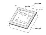
図1は本発明の実施の形態に係る半導体装置の構成を示す斜視図であり、図2は当該半導体装置の構成を示す側断面図である。半導体装置1は、単位基板となる半導体基板2を用いて構成されている。半導体基板2は、例えばシリコン基板からなるもので、平面視矩形に形成されている。本明細書で記述する「矩形」とは、意味的に長方形だけでなく正方形も含んでいる。半導体基板2は、平面的に見て、その外周側の領域を第1領域2Aとし、当該第1領域2Aよりも半導体基板2の内周側の領域を第2領域2Bとしている。第1領域2Aと第2領域2Bは、半導体装置1の製造工程の中で、特に、薄膜形成やドーピングなどのウエハ処理工程で区分されるものであるが、図1では説明の便宜上、第1領域2Aと第2領域2Bの境界を仮想的に破線で示している。 FIG. 1 is a perspective view showing a configuration of a semiconductor device according to an embodiment of the present invention, and FIG. 2 is a side sectional view showing a configuration of the semiconductor device. The
半導体基板2の第1領域2Aには、積層構造をなす渦巻き状のインダクタ3が形成され、半導体基板2の第2領域2Bには、例えば、集積回路を構成するトランジスタや抵抗、ダイオードなどの回路要素を含む回路部(集積回路部)4が形成されている。また、半導体基板2の第2領域2Bには複数の外部接続端子5が設けられている。各々の外部接続端子5は、後述する再配線の形成によって任意の位置に配置可能である。ここでは一例として、合計6つの外部接続端子5を2列に3つずつ並べて配置している。 In the
インダクタ3は、少なくとも2層の積層構造を有するものである。インダクタ3は、インダクタ配線を順に積層した状態で形成されるとともに、積層方向で隣り合うインダクタ配線の始端/終端を相互に接続することにより、全体として平面視矩形の渦巻き状に形成されている。本実施の形態においては、一例として、図2に示すように、第1の配線層7と、第2の配線層8と、第3の配線層9と、第4の配線層10とを含む、4層の多層配線構造を用いて、半導体基板2と一体にインダクタ3を形成している。 The inductor 3 has a laminated structure of at least two layers. The inductor 3 is formed in a state in which inductor wirings are sequentially stacked, and is formed in a spiral shape having a rectangular shape in plan view as a whole by connecting the start ends / terminal ends of adjacent inductor wirings in the stacking direction. In the present embodiment, as an example, as shown in FIG. 2, a
インダクタ3は、図示はしないが、第1の配線層7に含まれる第1のインダクタ配線と、第2の配線層8に含まれる第2のインダクタ配線と、第3の配線層9に含まれる第3のインダクタ配線と、第4の配線層10に含まれる第4のインダクタ配線とによって構成されるものである。各々のインダクタ配線は、主として、半導体基板2の第1領域2Aに形成・配置されるものである。インダクタ3の構成については、後段でさらに詳しく説明する。 Although not shown, the inductor 3 is included in the first inductor wiring included in the
第1の配線層7と第2の配線層8との間には、第1の絶縁膜11が形成されている。第2の配線層8と第3の配線層9との間には、第2の絶縁膜12が形成されている。第3の配線層9と第4の配線層10との間には、第3の絶縁膜13が形成されている。第1の配線層7と第2の配線層8との間の電気的な接続は、第1の絶縁膜11を貫通する状態で設けられたコンタクト部14によってなされている。第2の配線層8と第3の配線層9との間の電気的な接続は、第2の絶縁膜12を貫通する状態で設けられたコンタクト部15によってなされている。第3の配線層9と第4の配線層10との間の電気的な接続は、第3の絶縁膜13を貫通する状態で設けられたコンタクト部16によってなされている。コンタクト部14,15,16は、それぞれ回路構成上、必要に応じて複数個ずつ設けられるものである。 A first
回路部4には、半導体装置1の用途に応じて各種の機能回路を設けることができる。一例として、SAW(surface acoustic wave)フィルタ回路、FBAR(film bulk acoustic resonator)フィルタ回路などが考えられる。インダクタ3と回路部4内の回路は、図示しない配線で接続されている。SAWフィルタ回路とインダクタ3とを半導体基板2に設けた場合は、インダクタ3によるインピーダンスマッチングや波形整合が可能となる。 Various functional circuits can be provided in the circuit unit 4 according to the application of the
また、半導体基板2の第2領域2Bには、図示はしないが、第1の配線層7に含まれる第1の回路配線と、第2の配線層8に含まれる第2の回路配線と、第3の配線層9に含まれる第3の回路配線と、第4の配線層10に含まれる第4の回路配線が形成されている。各層の回路配線は、回路部4に含まれる回路要素同士を電気的に接続するものである。 Further, in the
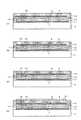
図3〜図5は本発明の実施の形態に係る半導体装置の製造方法を説明する工程図である。まず、図3(A)に示すように、ウエハ処理プロセスによってトランジスタ等の回路要素を作り終えた半導体基板2を用意する。回路要素は、半導体基板2の主面(図の上面)に形成され、図示しない絶縁性の保護膜で被覆されているものとする。この段階では、1枚のウエハの中に含まれる複数の単位基板の一つとして半導体基板2がウエハ面内に存在する。ウエハ面内は、最終的に個片(チップ)に分割される単位基板ごとに格子状に区分されている。このため、半導体基板2は、一つの区分(マス目)に存在する単位基板となる。 3 to 5 are process diagrams illustrating a method for manufacturing a semiconductor device according to an embodiment of the present invention. First, as shown in FIG. 3A, a
次に、図3(B)に示すように、半導体基板2の主面上に第1の配線層7を形成する。第1の配線層7は、例えば半導体基板2の主面上にアルミニウム等の金属を蒸着法によって所定の膜厚(例えば、1μm〜数μm)で成膜した後、マスクを用いて金属蒸着膜をエッチングすることにより得られる。このとき、金属蒸着膜の表面をエッチバックすることで、数百nmに薄膜化する。 Next, as shown in FIG. 3B, a
上記図3(B)に示す工程では、第1の配線層7により、上記第1領域2Aに第1のインダクタ配線を形成するとともに、上記第2領域2Bに第1の回路配線を形成する。すなわち、第1の配線層31は、前述したように第1のインダクタ配線と第1の回路配線の両方を含むものとなる。このため、第1のインダクタ配線と第1の回路配線は、同じ工程で同じ層に形成されるものとなる。第1の回路配線としては、例えば、トランジスタ、抵抗及びシリコン基板内の拡散領域から取り出す電極や配線などが考えられる。 In the step shown in FIG. 3B, the
次に、図3(C)に示すように、半導体基板2の主面上に第1の配線層7を覆う状態で第1の絶縁膜11を形成する。第1の絶縁膜11は、例えば酸化シリコン膜からなるもので、例えばCVD法により1μmの膜厚で形成される。 Next, as shown in FIG. 3C, a first insulating
次に、図3(D)に示すように、第1の絶縁膜11に開口部21を形成する。開口部21は、第1の配線層7の配線上でかつ配線幅の中央部を外部に露出する状態で形成される。開口部21は、例えばウェットエッチングやドライエッチングなどの方法により、穴径(直径)が5μm〜数十μmの大きさで形成される。 Next, as illustrated in FIG. 3D, an
次に、図3(E)に示すように、半導体基板2の主面上に第2の配線層8を形成する。第2の配線層8は、例えば上記第1の配線層7と同様に、半導体基板2の主面上にアルミニウム等の金属を蒸着法によって所定の膜厚(例えば、1μm〜数μm)で成膜した後、マスクを用いて金属蒸着膜をエッチングすることにより得られる。このとき、上記開口部21は、金属蒸着により第2の配線層8と同じ材料で埋め込まれる。これにより、第1の絶縁膜11中にコンタクト部14が形成される。コンタクト部14は、第1の配線層7と第2の配線層8とを電気的に接続するために適所に設けられるものである。 Next, as shown in FIG. 3E, a
上記図3(E)に示す工程では、第2の配線層8により、上記第1領域2Aに第2のインダクタ配線を形成するとともに、上記第2領域2Bに第2の回路配線を形成する。すなわち、第2の配線層8は、前述したように第2のインダクタ配線と第2の回路配線の両方を含むものとなる。このため、第2のインダクタ配線と第2の回路配線は、同じ工程で同じ層に形成されるものとなる。第2の回路配線としては、例えば、トランジスタ、抵抗等から取り出した電極の端子・配線間を接続する再配線などが考えられる。 In the step shown in FIG. 3E, the
次に、図4(A)に示すように、半導体基板2の主面上でかつ第1の絶縁膜11の上に第2の配線層8を覆う状態で第2の絶縁膜12を積層状態に形成する。第2の絶縁膜12は、例えば上記第1の絶縁膜11と同様に酸化シリコン膜からなるもので、例えばCVD法により1μmの膜厚で形成される。 Next, as shown in FIG. 4A, the second insulating
次に、図4(B)に示すように、第2の絶縁膜12に開口部22を形成する。開口部22は、上記開口部21とは平面的に異なる位置に形成される。また、開口部22は、第2の配線層8の配線上でかつ配線幅の中央部を外部に露出する状態で形成される。開口部22は、例えば上記開口部21と同様にウェットエッチングやドライエッチングなどの方法により、穴径(直径)が5μm〜数十μmの大きさで形成される。 Next, as illustrated in FIG. 4B, an
次に、図4(C)に示すように、上記開口部22を金属材料で埋め込むことにより、当該開口部22にコンタクト部15を形成する。コンタクト部15は、例えば上記開口部22を埋め込む状態で第2の絶縁膜12の上面にチタンとニッケルを順に蒸着した後、不要な金属膜を平坦化研磨(CMP等)によって除去することにより形成される。 Next, as shown in FIG. 4C, the
次に、図4(D)に示すように、半導体基板2の主面上でかつ第2の絶縁膜12の上に第3の配線層9を形成する。第3の配線層9は、例えば第2の絶縁膜12の上に銅配線を蒸着することにより形成される。 Next, as shown in FIG. 4D, a
上記図4(D)に示す工程では、第3の配線層9により、上記第1領域2Aに第3のインダクタ配線を形成するとともに、上記第2領域2Bに第3の回路配線を形成する。すなわち、第3の配線層9は、前述したように第3のインダクタ配線と第3の回路配線の両方を含むものとなる。このため、第3のインダクタ配線と第3の回路配線は、同じ工程で同じ層に形成されるものとなる。第3の回路配線としては、例えば、上記第2の回路配線で接続した素子ブロックや回路ブロックの配線間を接続する再配線などが考えられる。 In the step shown in FIG. 4D, the third inductor layer is formed in the
次に、図5(A)に示すように、半導体基板2の主面上でかつ第2の絶縁膜12の上に第3の配線層9を覆う状態で第3の絶縁膜13を形成する。第3の絶縁膜13は、ウエハ・レベルCSPを実現するための樹脂層を構成するものである。ウエハ・レベルCSPとは、ウエハの状態で、再配線や保護膜、端子の形成を行ない、その後で個片化したパッケージ(半導体装置)をいい、パッケージの実装面積が半導体チップと同じ大きさになる。第3の絶縁膜13は、例えば、ウエハの大きさやサイズに合わせた金型を用いて、ウエハの上面だけに液状の樹脂(例えば、エポキシ系の樹脂)を流し込んで数百μm程度に積層し硬化することにより形成される。 Next, as shown in FIG. 5A, a third insulating
次に、図5(B)に示すように、第3の絶縁膜13に開口部23を形成する。開口部23は、上記開口部22とは平面的に異なる位置に形成される。また、開口部23は、第3の配線層9の配線上でかつ配線幅の中央部を外部に露出する状態で形成される。 Next, as shown in FIG. 5B, an
次に、図5(C)に示すように、上記開口部23を金属材料で埋め込むことにより、当該開口部23にコンタクト部16を形成する。 Next, as shown in FIG. 5C, the
次に、図5(D)に示すように、半導体基板2の主面上でかつ第3の絶縁膜13の上に第4の配線層10を形成する。第4の配線層10は、例えば第3の絶縁膜13の上に銅配線を蒸着することにより形成される。 Next, as shown in FIG. 5D, the
上記図5(D)に示す工程では、第4の配線層10により、第1領域2Aに第4のインダクタ配線を形成するとともに、第2領域2Bに第4の回路配線を形成する。すなわち、第4の配線層10は、前述したように第4のインダクタ配線と第4の回路配線を含むものとなる。このため、第4のインダクタ配線と第4の回路配線は、同じ工程で同じ層に形成されるものとなる。第4の回路配線としては、例えば、上記第3の回路配線の終端で第3の絶縁膜13を貫通する外部接続端子5が考えられる。 In the step shown in FIG. 5D, the
以上の製造工程を経て作製された半導体基板2をウエハ状態からダイシング等によって個片化することにより、上記図1に示すような外観の半導体装置(パッケージ)1が得られる。なお、各々の外部接続端子5上には、上記個片化の前に、必要に応じて、バンプが形成される。 A semiconductor device (package) 1 having an appearance as shown in FIG. 1 is obtained by dividing the
本発明の実施の形態に係る半導体装置の製造方法においては、半導体基板2の第2領域2Bに回路配線を形成する工程と同じ工程のなかで、半導体基板2の第1領域2Aにインダクタ配線を形成するため、実質的に半導体装置の製造工程数を増やすことなく、インダクタ3を内蔵した半導体装置1を製造することができる。また、半導体基板2の外周側の領域を第1領域2Aとし、この第1領域2Aに積層構造をなす渦巻き状のインダクタ3を形成するため、例えば第2領域2Bに単層構造で渦巻き状にインダクタを形成する場合に比較して、インダクタンス値を大幅に上昇させることができる。 In the method for manufacturing a semiconductor device according to the embodiment of the present invention, the inductor wiring is formed in the
ここで、上記製造方法によって得られる4層構造のインダクタ3の構成について説明する。前述した第1〜第4のインダクタ配線のうち、積層方向で隣り合う二つのインダクタ配線(例えば、第1のインダクタ配線と第2のインダクタ配線)は、互いに異なる配線パターンで形成されている。ただし、第1のインダクタ配線と第3のインダクタ配線は、互いに同じ配線パターンで形成され、第2のインダクタ配線と第4のインダクタ配線も、互いに同じ配線パターンで形成されている。つまり、インダクタ3の積層数をn層(nは自然数)とすると、奇数層に形成されたインダクタ配線と偶数層に形成されたインダクタ配線は、互いに異なる配線パターンで形成されている。また、奇数層に形成されたインダクタ配線はすべて同じ配線パターンで形成され、偶数層に形成されたインダクタ配線もすべて同じ配線パターンで形成されている。 Here, the configuration of the inductor 3 having a four-layer structure obtained by the above manufacturing method will be described. Of the first to fourth inductor wirings described above, two inductor wirings adjacent to each other in the stacking direction (for example, the first inductor wiring and the second inductor wiring) are formed with mutually different wiring patterns. However, the first inductor wiring and the third inductor wiring are formed with the same wiring pattern, and the second inductor wiring and the fourth inductor wiring are also formed with the same wiring pattern. That is, if the number of stacked inductors 3 is n (n is a natural number), the inductor wiring formed in the odd layer and the inductor wiring formed in the even layer are formed with different wiring patterns. Further, all the inductor wirings formed in the odd layers are formed with the same wiring pattern, and all the inductor wirings formed in the even layers are also formed with the same wiring pattern.
このため、第1〜第4のインダクタ配線は、2種類の配線パターンを交互に適用して形成されることになる。本実施の形態においては、上記2種類の配線パターンとして、図6(A)に示す配線パターン(以下、「第1のインダクタ配線パターン」)25と、図6(B)に示す配線パターン(以下、「第2のインダクタ配線パターン」)26とを採用している。インダクタ3を構成するインダクタ配線の配線幅を広くすると、インダクタ3のQ値を上昇させることが可能である。 For this reason, the first to fourth inductor wirings are formed by alternately applying two types of wiring patterns. In the present embodiment, as the two types of wiring patterns, the wiring pattern shown in FIG. 6A (hereinafter referred to as “first inductor wiring pattern”) 25 and the wiring pattern shown in FIG. , “Second inductor wiring pattern”) 26. When the wiring width of the inductor wiring constituting the inductor 3 is increased, the Q value of the inductor 3 can be increased.
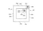
第1のインダクタ配線パターン25は、主として、半導体基板2の第1領域2Aに形成されるものである。第1のインダクタ配線パターン25は、半導体基板2の4つの辺に沿う、連続した4つの直線パターン25a〜25dと1つの突出パターン25eとを有している。4つの直線パターン25a〜25dは、上記半導体基板2の第1領域2Aに形成されるものである。4つの直線パターン25a〜25dのうち、相対応する2つの直線パターン同士、すなわち直線パターン25aと直線パターン25cは互いに平行に配置され、直線パターン25bと直線パターン25dも互いに平行に配置されている。また、直線パターン25aと直線パターン25bは直角をなして配置され、直線パターン25cと直線パターン25dも直角をなして配置されている。 The first
突出パターン25eは、上記半導体基板2の第1領域2Aから第2領域2B側(半導体基板2の内周側)に突出する状態に形成されるものである。突出パターン25eの突出端は、上記第1領域2Aに配置されていてもよいし、上記第2領域2Bに配置されていてもよい。突出パターン25eは、直線パターン25aとは物理的に分離(電気的に絶縁)した状態で、直線パターン25dの一端部から直線パターン25aに沿って直角(鍵型)に折れ曲がる状態で配置されている。このため、直線パターン25dの長さは、他の3つの直線パターン25a,25b,25cの長さよりも短くなっている。また、突出パターン25eは、4つの直線パターン25a〜25dで囲まれた内側の領域内(直線パターン25bに近づく方向)に突出する状態で配置されている。 The protruding
第1のインダクタ配線パターン25の始端と終端には、それぞれ接続部27a,27bが設けられている。第1のインダクタ配線パターン25の始端とは、渦巻き状のインダクタ3を構成するインダクタ配線の巻線方向(コイル巻線方向)において、上流側の配線端をいう。第1のインダクタ配線パターン25の終端とは、渦巻き状のインダクタ3を構成するインダクタ配線の巻線方向において、下流側の配線端をいう。インダクタ配線の巻線方向は、インダクタ3に流れる電流の方向で規定されるものである。ここでは、一例として、一方の接続部27aを第1のインダクタ配線パターン25の始端とし、もう一方の接続部27bを第1のインダクタ配線パターン25の終端とする。
第2のインダクタ配線パターン26は、主として、半導体基板2の第1領域2Aに形成されるものである。第2のインダクタ配線パターン26は、半導体基板2の4つの辺に沿う、連続した4つの直線パターン26a〜26dと1つの突出パターン26eとを有している。4つの直線パターン26a〜26dは、上記半導体基板2の第1領域2Aに形成されるものである。4つの直線パターン26a〜26dのうち、相対応する2つの直線パターン同士、すなわち直線パターン26aと直線パターン26cは互いに平行に配置され、直線パターン26bと直線パターン26dも互いに平行に配置されている。また、直線パターン26aと直線パターン26bは直角をなして配置され、直線パターン26cと直線パターン26dも直角をなして配置されている。 The second
突出パターン26eは、上記半導体基板2の第1領域2Aから第2領域2B側(半導体基板2の内周側)に突出する状態に形成されるものである。突出パターン26eの突出端は、上記第1領域2Aに配置されていてもよいし、上記第2領域2Bに配置されていてもよい。突出パターン26eは、直線パターン26dとは物理的に分離(電気的に絶縁)した状態で、直線パターン26aの一端部から直線パターン26dに沿って直角(鍵型)に折れ曲がる状態で配置されている。このため、直線パターン26aの長さは、他の3つの直線パターン26b,26c,26dの長さよりも短くなっている。また、突出パターン26eは、4つの直線パターン26a〜26dで囲まれた内側の領域内(直線パターン26cに近づく方向)に突出する状態で配置されている。 The protruding
第2のインダクタ配線パターン26の始端には接続部28aが設けられ、第2のインダクタ配線パターン26の終端には接続部28bが設けられている。本実施の形態においては、一例として、第1のインダクタ配線と第3のインダクタ配線を第1のインダクタ配線パターン25を適用して形成するとともに、第2のインダクタ配線と第4のインダクタ配線を第2のインダクタ配線パターン26を適用して形成するものとする。 A
そうした場合、第1のインダクタ配線と第2のインダクタ配線との間では、第1のインダクタ配線パターン25終端の接続部27bが、前述したコンタクト部14を介して、第2のインダクタ配線パターン26始端の接続部28aに電気的に接続されることになる。また、第2のインダクタ配線と第3のインダクタ配線との間では、第2のインダクタ配線パターン26終端の接続部28bが、前述したコンタクト部15を介して、第1のインダクタ配線パターン25始端の接続部27aに電気的に接続されることなる。また、第3のインダクタ配線と第4のインダクタ配線との間では、第1のインダクタ配線パターン25終端の接続部27bが、前述したコンタクト部16を介して、第2のインダクタ配線パターン26始端の接続部28aに電気的に接続されることになる。 In such a case, between the first inductor wiring and the second inductor wiring, the
上記構成からなる第1のインダクタ配線パターン25は、全体的に平面視略G字形に形成されている。これに対して、第2のインダクタ配線パターン26は、上記図6(A)に示す状態から第1のインダクタ配線パターン25を反時計回り方向に90度回転させた後、当該第1のインダクタ配線パターン25の中心を通る縦の基準軸Kを境に、上記90度回転後の第1のインダクタ配線パターン25を左右反転させた形状と同一形状となっている。このため、第1のインダクタ配線パターン25と第2のインダクタ配線パターン26とは、基本的に配線幅、配線長さなどが同じ寸法で設定されている。また、第1のインダクタ配線パターン25における接続部27A,27Bの位置関係と、第2のインダクタ配線パターン26における接続部28A,28Bの位置関係も、同じ関係になっている。 The first
このため、積層方向で隣り合う2つの配線層の間で、第1のインダクタ配線パターン25と第2のインダクタ配線パターン26を重ね合わせると、図7のような配置関係となる。この図7においては、説明の便宜上、配線パターンの位置を意図的にずらして表示している。図から分かるように、第1のインダクタ配線パターン25と第2のインダクタ配線パターン26は、相対応する直線パターン同士(25aと26a、25bと26b、25cと26c、25dと26d)が重なり合っている。また、第1のインダクタ配線パターン25の接続部27aは第2のインダクタ配線26の接続部28bに重なり合い、第1のインダクタ配線パターン25の接続部27bは第2のインダクタ配線26の接続部28aに重なり合っている。 Therefore, when the first
図8はインダクタ配線の相互の接続状態を示す斜視図である。インダクタ3は、第1のインダクタ配線31と、第2のインダクタ配線32と、第3のインダクタ配線33と、第4のインダクタ配線34とを用いて構成されている。第1のインダクタ配線31及び第3のインダクタ配線33には、それぞれ上記突出パターン25eに相当する突出部31a,33aが設けられている。第2のインダクタ配線32及び第4のインダクタ配線34には、それぞれ上記突出パターン26eに相当する突出部32a,34aが設けられている。各々の突出部31a〜34aは、半導体基板2の角(かど)部で互いに重なり合う状態に配置されている。そして、突出部31a,32aは、上記コンタクト部14を介して電気的に接続され、突出部32a,33aは、上記コンタクト部15を介して電気的に接続され、突出部33a,34aは、上記コンタクト部16を介して電気的に接続されている。これにより、積層方向で隣り合うインダクタ配線の始端/終端は、半導体基板2の角部で相互に接続された構成となっている。 FIG. 8 is a perspective view showing a connection state of inductor wirings. The inductor 3 includes a
このような4層構造のインダクタ3を半導体基板2の外形に沿う渦巻き状にして第1領域2Aに組み込むことにより、ウエハ・レベルCSPという非常に小型の半導体装置1であっても、比較的大きなインダクタンス値をもつインダクタを実現することができる。実際に4層構造のインダクタ3に関して、半導体基板2の大きさ(外形)を1mm角(1mm×1mm)とし、インダクタ配線の配線幅を100μmとし、インダクタ配線の厚さを10μmとして、シミュレーションしたところ、20nH程度のインダクタンス値をもつインダクタを実現できることが分かった。また、3mm角の半導体基板2を用いて、上記同様の条件でインダクタ配線を形成した場合は、100nHを超えるインダクタンス値をもつインダクタを実現できることが分かった。 By incorporating such an inductor 3 having a four-layer structure in a spiral shape along the outer shape of the
また、半導体基板2の外周側の第1領域2Aに複数のインダクタ配線を積層してインダクタ3を形成することにより、インダクタ3を構成する各層のインダクタ配線の存在により、個片化した後の半導体装置1の応力を緩和することができる。このため、半導体基板2の第2領域2Bに形成された回路部4のひずみ(特に、反り)を軽減し、回路特性の変動を抑制することができる。 Further, by forming the inductor 3 by laminating a plurality of inductor wirings in the
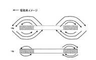
ここで、インダクタ配線の接続形態が異なる2種類のインダクタの特性上の違いについて説明する。一つは、上記実施の形態と同様に、図9(A)に示すように、積層方向で隣り合うインダクタ配線の始端/終端を一箇所にまとめて配置し、それらの始端/終端を、半導体基板2の角部で相互に接続した構造のインダクタとする。もう一つは、図9(B)に示すように、積層方向で隣り合うインダクタ配線の始端/終端を、層ごとにインダクタ配線パターンの長さ方向に位置をずらして配置し、各々の位置で始端/終端を相互に接続した構造のインダクタとする。 Here, a difference in characteristics between two types of inductors having different connection forms of the inductor wiring will be described. As shown in FIG. 9A, the first is to arrange the start ends / ends of inductor wirings adjacent in the stacking direction in one place, as shown in FIG. The inductor is structured to be connected to each other at the corners of the
図10は上記図9(A)に示すインダクタの磁界分布を示す図である。図11は、上記図9(B)に示すインダクタの磁界分布を示す図である。また、図12は上記図9(A)に示すインダクタの磁界分布をX軸上及びY軸上で断面的に見た場合の電磁束のイメージを示す図であり、図13は上記図9(B)に示すインダクタの磁界分布をX軸上及びY軸上で断面的に見た場合の電磁束のイメージを示す図である。図から分かるように、図9(A)に示すインダクタの磁界分布では、電磁束が均一になっているのに対して、図9(B)に示すインダクタの磁界分布では、電磁束が不均一になっている。この磁束分布の違いは、インダクタを構成するインダクタ配線の積層厚のばらつきによるものである。 FIG. 10 is a diagram showing the magnetic field distribution of the inductor shown in FIG. FIG. 11 is a diagram showing the magnetic field distribution of the inductor shown in FIG. 9B. FIG. 12 is a diagram showing an image of electromagnetic flux when the magnetic field distribution of the inductor shown in FIG. 9A is viewed in cross section on the X-axis and the Y-axis, and FIG. It is a figure which shows the image of the electromagnetic flux at the time of seeing the magnetic field distribution of the inductor shown to B) in cross section on an X-axis and a Y-axis. As can be seen from the figure, in the magnetic field distribution of the inductor shown in FIG. 9A, the electromagnetic flux is uniform, whereas in the magnetic field distribution of the inductor shown in FIG. 9B, the electromagnetic flux is not uniform. It has become. This difference in magnetic flux distribution is due to variations in the laminated thickness of the inductor wiring constituting the inductor.
図14(A)は上記図9(A)に示すインダクタのインピーダンス整合特性を示すスミスチャートであり、図14(B)は上記図9(B)に示すインダクタのインピーダンス整合特性を示すスミスチャートである。図14(A)に示すスミスチャートでは、インダクタの特性を示す曲線が良好に回転しているのに対して、図14(B)に示すスミスチャートでは、インダクタの特性を示す曲線が十分に回転していない。このため、前者のインダクタの方が、高周波のインピーダンス整合がとりやすくなる。また、前者のインダクタにおいては、配線内での磁束の変化を抑えることができることができる。このため、各層間の結合係数が大きくなり、自己インダクタンス値が大きいスパイラルインダクタを実現することができる。したがって、MMICなどの通信用ICに好適に用いることができる。 14A is a Smith chart showing the impedance matching characteristics of the inductor shown in FIG. 9A, and FIG. 14B is a Smith chart showing the impedance matching characteristics of the inductor shown in FIG. 9B. is there. In the Smith chart shown in FIG. 14A, the curve indicating the inductor characteristics rotates well, whereas in the Smith chart shown in FIG. 14B, the curve indicating the inductor characteristics rotates sufficiently. Not done. For this reason, the former inductor is easier to achieve high-frequency impedance matching. Further, in the former inductor, a change in magnetic flux in the wiring can be suppressed. For this reason, it is possible to realize a spiral inductor having a large coupling coefficient between the respective layers and a large self-inductance value. Therefore, it can be suitably used for a communication IC such as an MMIC.
なお、上記実施の形態においては、4層構造のインダクタ3を例示したが、インダクタの積層構造はこれに限らず、2層構造であっても、3層構造であっても、5層以上の多層構造であってもよい。このため、半導体基板2上に複数の配線層を形成するにあたっては、第1のインダクタ配線パターン25を適用してインダクタ配線を形成する工程と、第2のインダクタ配線パターン26を適用してインダクタ配線を形成する工程とを、少なくとも1回ずつ行なうことにより、第1領域2Aに積層構造をなす渦巻き状のインダクタ3を形成することになる。 In the above embodiment, the inductor 3 having a four-layer structure is illustrated. However, the laminated structure of the inductor is not limited to this, and a five-layer or more structure is possible regardless of whether the two-layer structure or the three-layer structure. A multilayer structure may be used. For this reason, when forming a plurality of wiring layers on the
また、2層構造のインダクタ3を形成する場合は、第1の配線層7〜第4の配線層10のうち、積層方向で隣り合う2つの配線層により、2層構造のインダクタ3を形成すればよい。また、3層構造のインダクタ3を形成する場合は、第1の配線層7〜第4の配線層10のうち、積層方向で隣り合う3つの配線層により、3層構造のインダクタ3を形成すればよい。また、5層構造のインダクタ3を形成する場合は、半導体基板2に形成する配線層の層数を5層以上に増やして、積層方向で隣り合う5つの配線層により、5層構造のインダクタ3を形成すればよい。 When the inductor 3 having the two-layer structure is formed, the inductor 3 having the two-layer structure is formed by two wiring layers adjacent in the stacking direction among the first to
1…半導体装置、2…半導体基板(単位基板)、3…インダクタ、4…回路部 DESCRIPTION OF
Claims (4)
Translated fromJapanese前記単位基板上に前記第1のインダクタ配線に電気的に接続する第2のインダクタ配線と前記第1の回路配線に電気的に接続する第2の回路配線とを形成する工程とを、
少なくとも1回ずつ行なうことにより、前記単位基板上に積層構造をなす渦巻き状のインダクタを形成する
半導体装置の製造方法。Forming a first inductor wiring and a first circuit wiring on a unit substrate;
Forming a second inductor wiring electrically connected to the first inductor wiring and a second circuit wiring electrically connected to the first circuit wiring on the unit substrate;
A method of manufacturing a semiconductor device, wherein a spiral inductor having a laminated structure is formed on the unit substrate by performing at least once.
前記第1領域よりも前記単位基板の内周側の領域を第2領域として、
前記第1領域に前記第1のインダクタ配線と前記第2のインダクタ配線を形成し、
前記第2領域に前記第1の回路配線と前記第2の回路配線を形成する
請求項1記載の半導体装置の製造方法。A region on the outer peripheral side of the unit substrate is a first region,
A region on the inner peripheral side of the unit substrate from the first region is a second region,
Forming the first inductor wiring and the second inductor wiring in the first region;
The method for manufacturing a semiconductor device according to claim 1, wherein the first circuit wiring and the second circuit wiring are formed in the second region.
前記第1領域よりも前記単位基板の内周側の領域を第2領域として、
前記第1領域に形成された、積層構造をなす渦巻き状のインダクタと、
前記第2領域に形成された回路部と
を備える半導体装置。The area on the outer peripheral side of the unit substrate is the first area,
A region on the inner peripheral side of the unit substrate from the first region is a second region,
A spiral inductor having a laminated structure formed in the first region;
A semiconductor device comprising: a circuit unit formed in the second region.
請求項3記載の半導体装置。The inductor is formed by sequentially laminating a plurality of inductor wirings, and the start / ends of two inductor wirings adjacent in the stacking direction are connected to each other at the corners of the unit substrate having a rectangular shape in plan view. The semiconductor device according to claim 3.
Priority Applications (1)
| Application Number | Priority Date | Filing Date | Title |
|---|---|---|---|
| JP2008112024AJP2009266908A (en) | 2008-04-23 | 2008-04-23 | Method for manufacturing semiconductor device and semiconductor device |
Applications Claiming Priority (1)
| Application Number | Priority Date | Filing Date | Title |
|---|---|---|---|
| JP2008112024AJP2009266908A (en) | 2008-04-23 | 2008-04-23 | Method for manufacturing semiconductor device and semiconductor device |
Publications (1)
| Publication Number | Publication Date |
|---|---|
| JP2009266908Atrue JP2009266908A (en) | 2009-11-12 |
Family
ID=41392413
Family Applications (1)
| Application Number | Title | Priority Date | Filing Date |
|---|---|---|---|
| JP2008112024APendingJP2009266908A (en) | 2008-04-23 | 2008-04-23 | Method for manufacturing semiconductor device and semiconductor device |
Country Status (1)
| Country | Link |
|---|---|
| JP (1) | JP2009266908A (en) |
Cited By (5)
| Publication number | Priority date | Publication date | Assignee | Title |
|---|---|---|---|---|
| WO2011021411A1 (en)* | 2009-08-21 | 2011-02-24 | 株式会社村田製作所 | Esd protection device |
| JP2017504212A (en)* | 2014-01-21 | 2017-02-02 | クアルコム,インコーポレイテッド | Annular inductors in the redistribution layer of integrated devices |
| CN108346642A (en)* | 2018-04-13 | 2018-07-31 | 安徽云塔电子科技有限公司 | A kind of inductance stacked structure |
| JP2021510457A (en)* | 2018-10-17 | 2021-04-22 | 安徽安努奇科技有限公司Anhui Anuki Technologies Co., Ltd. | Chip inductor and its manufacturing method |
| JP2021510935A (en)* | 2018-04-13 | 2021-04-30 | 安徽▲雲▼塔▲電▼子科技有限公司 | Inductor laminated structure |
- 2008
- 2008-04-23JPJP2008112024Apatent/JP2009266908A/enactivePending
Cited By (7)
| Publication number | Priority date | Publication date | Assignee | Title |
|---|---|---|---|---|
| WO2011021411A1 (en)* | 2009-08-21 | 2011-02-24 | 株式会社村田製作所 | Esd protection device |
| JP2017504212A (en)* | 2014-01-21 | 2017-02-02 | クアルコム,インコーポレイテッド | Annular inductors in the redistribution layer of integrated devices |
| CN108346642A (en)* | 2018-04-13 | 2018-07-31 | 安徽云塔电子科技有限公司 | A kind of inductance stacked structure |
| JP2021510935A (en)* | 2018-04-13 | 2021-04-30 | 安徽▲雲▼塔▲電▼子科技有限公司 | Inductor laminated structure |
| US11631516B2 (en) | 2018-04-13 | 2023-04-18 | Anhui Yunta Electronic Technologies Co., Ltd. | Inductor stack structure |
| JP2021510457A (en)* | 2018-10-17 | 2021-04-22 | 安徽安努奇科技有限公司Anhui Anuki Technologies Co., Ltd. | Chip inductor and its manufacturing method |
| US12094631B2 (en) | 2018-10-17 | 2024-09-17 | Anhui Anuki Technologies Co., Ltd. | Chip inductor and method for manufacturing same |
Similar Documents
| Publication | Publication Date | Title |
|---|---|---|
| JP5206775B2 (en) | Electronic components | |
| JP5195876B2 (en) | Coil component and manufacturing method thereof | |
| JP6935343B2 (en) | Inductor parts and their manufacturing methods | |
| JP5093210B2 (en) | Coil component and manufacturing method thereof | |
| US8451083B2 (en) | Coil component and method of manufacturing the same | |
| JP5673359B2 (en) | Coil component and manufacturing method thereof | |
| US9214270B2 (en) | Electronic component and manufacturing method thereof | |
| JP5737313B2 (en) | Electronic component and manufacturing method thereof | |
| JP4922353B2 (en) | Coil component and manufacturing method thereof | |
| CN1691220B (en) | coil parts | |
| TWI302715B (en) | Symmetrical inductor | |
| CN112908611B (en) | Coil component | |
| US8581684B2 (en) | Multiple-level inductance | |
| JP5500186B2 (en) | Coil component and manufacturing method thereof | |
| JP2009266908A (en) | Method for manufacturing semiconductor device and semiconductor device | |
| CN114127971A (en) | Techniques, electronic systems, and methods for fabricating integrated inductors and related semiconductor devices | |
| JP6838635B2 (en) | Coil parts | |
| JP2005044952A (en) | Common mode choke coil and manufacturing method thereof, and common mode choke coil array | |
| JP2008091631A (en) | Semiconductor device | |
| JP2004335761A (en) | Inductor device | |
| JPH0950916A (en) | Thin film magnetic element | |
| JP2003297633A (en) | Laminated component | |
| JP7411590B2 (en) | Inductor parts and their manufacturing method | |
| US20250201688A1 (en) | Integrated passive component, and manufacturing method for integrated passive component | |
| JPWO2017057423A1 (en) | Surface mount LC device |