JP2009253166A - Optical communication module - Google Patents
Optical communication moduleDownload PDFInfo
- Publication number
- JP2009253166A JP2009253166AJP2008101809AJP2008101809AJP2009253166AJP 2009253166 AJP2009253166 AJP 2009253166AJP 2008101809 AJP2008101809 AJP 2008101809AJP 2008101809 AJP2008101809 AJP 2008101809AJP 2009253166 AJP2009253166 AJP 2009253166A
- Authority
- JP
- Japan
- Prior art keywords
- photoelectric conversion
- conversion element
- optical fiber
- communication module
- optical communication
- Prior art date
- Legal status (The legal status is an assumption and is not a legal conclusion. Google has not performed a legal analysis and makes no representation as to the accuracy of the status listed.)
- Abandoned
Links
- 230000003287optical effectEffects0.000titleclaimsabstractdescription80
- 238000004891communicationMethods0.000titleclaimsabstractdescription54
- 239000013307optical fiberSubstances0.000claimsabstractdescription66
- 238000006243chemical reactionMethods0.000claimsabstractdescription61
- 229920005989resinPolymers0.000claimsabstractdescription49
- 239000011347resinSubstances0.000claimsabstractdescription49
- 230000008878couplingEffects0.000claimsabstractdescription16
- 238000010168coupling processMethods0.000claimsabstractdescription16
- 238000005859coupling reactionMethods0.000claimsabstractdescription16
- 238000003384imaging methodMethods0.000claimsdescription9
- 230000000149penetrating effectEffects0.000claimsdescription4
- 238000007789sealingMethods0.000description10
- 239000000758substrateSubstances0.000description9
- 239000000463materialSubstances0.000description5
- 238000000034methodMethods0.000description4
- 238000004519manufacturing processMethods0.000description3
- 239000000470constituentSubstances0.000description2
- 239000003822epoxy resinSubstances0.000description2
- 230000004048modificationEffects0.000description2
- 238000012986modificationMethods0.000description2
- 229920000647polyepoxidePolymers0.000description2
- RYGMFSIKBFXOCR-UHFFFAOYSA-NCopperChemical compound[Cu]RYGMFSIKBFXOCR-UHFFFAOYSA-N0.000description1
- 239000000853adhesiveSubstances0.000description1
- 230000001070adhesive effectEffects0.000description1
- 230000005540biological transmissionEffects0.000description1
- 229910052802copperInorganic materials0.000description1
- 239000010949copperSubstances0.000description1
- 238000010586diagramMethods0.000description1
- 230000010354integrationEffects0.000description1
- 238000000465mouldingMethods0.000description1
- 239000004033plasticSubstances0.000description1
- 229920003023plasticPolymers0.000description1
- 229920003229poly(methyl methacrylate)Polymers0.000description1
- 239000004926polymethyl methacrylateSubstances0.000description1
- 238000005476solderingMethods0.000description1
- 229920001187thermosetting polymerPolymers0.000description1
Images


Classifications
- G—PHYSICS
- G02—OPTICS
- G02B—OPTICAL ELEMENTS, SYSTEMS OR APPARATUS
- G02B6/00—Light guides; Structural details of arrangements comprising light guides and other optical elements, e.g. couplings
- G02B6/24—Coupling light guides
- G02B6/42—Coupling light guides with opto-electronic elements
- G02B6/4201—Packages, e.g. shape, construction, internal or external details
- G02B6/4204—Packages, e.g. shape, construction, internal or external details the coupling comprising intermediate optical elements, e.g. lenses, holograms
- G—PHYSICS
- G02—OPTICS
- G02B—OPTICAL ELEMENTS, SYSTEMS OR APPARATUS
- G02B6/00—Light guides; Structural details of arrangements comprising light guides and other optical elements, e.g. couplings
- G02B6/24—Coupling light guides
- G02B6/42—Coupling light guides with opto-electronic elements
- G02B6/4201—Packages, e.g. shape, construction, internal or external details
- G02B6/4202—Packages, e.g. shape, construction, internal or external details for coupling an active element with fibres without intermediate optical elements, e.g. fibres with plane ends, fibres with shaped ends, bundles
- G—PHYSICS
- G02—OPTICS
- G02B—OPTICAL ELEMENTS, SYSTEMS OR APPARATUS
- G02B6/00—Light guides; Structural details of arrangements comprising light guides and other optical elements, e.g. couplings
- G02B6/24—Coupling light guides
- G02B6/42—Coupling light guides with opto-electronic elements
- G02B6/4201—Packages, e.g. shape, construction, internal or external details
- G02B6/4219—Mechanical fixtures for holding or positioning the elements relative to each other in the couplings; Alignment methods for the elements, e.g. measuring or observing methods especially used therefor
- G02B6/4236—Fixing or mounting methods of the aligned elements
- G02B6/424—Mounting of the optical light guide
- G—PHYSICS
- G02—OPTICS
- G02B—OPTICAL ELEMENTS, SYSTEMS OR APPARATUS
- G02B6/00—Light guides; Structural details of arrangements comprising light guides and other optical elements, e.g. couplings
- G02B6/24—Coupling light guides
- G02B6/42—Coupling light guides with opto-electronic elements
- G02B6/4201—Packages, e.g. shape, construction, internal or external details
- G02B6/4219—Mechanical fixtures for holding or positioning the elements relative to each other in the couplings; Alignment methods for the elements, e.g. measuring or observing methods especially used therefor
- G02B6/4236—Fixing or mounting methods of the aligned elements
- G02B6/4245—Mounting of the opto-electronic elements
- G—PHYSICS
- G02—OPTICS
- G02B—OPTICAL ELEMENTS, SYSTEMS OR APPARATUS
- G02B6/00—Light guides; Structural details of arrangements comprising light guides and other optical elements, e.g. couplings
- G02B6/24—Coupling light guides
- G02B6/42—Coupling light guides with opto-electronic elements
- G02B6/4201—Packages, e.g. shape, construction, internal or external details
- G02B6/4251—Sealed packages
- G02B6/4253—Sealed packages by embedding housing components in an adhesive or a polymer material
- G—PHYSICS
- G02—OPTICS
- G02B—OPTICAL ELEMENTS, SYSTEMS OR APPARATUS
- G02B6/00—Light guides; Structural details of arrangements comprising light guides and other optical elements, e.g. couplings
- G02B6/24—Coupling light guides
- G02B6/42—Coupling light guides with opto-electronic elements
- G02B6/4201—Packages, e.g. shape, construction, internal or external details
- G02B6/4256—Details of housings
Landscapes
- Physics & Mathematics (AREA)
- General Physics & Mathematics (AREA)
- Optics & Photonics (AREA)
- Optical Couplings Of Light Guides (AREA)
- Led Device Packages (AREA)
Abstract
Translated fromJapaneseDescription
Translated fromJapanese本発明は、光ファイバーと、光電変換素子パッケージとを光学的に結合するための光通信モジュールに関するものである。 The present invention relates to an optical communication module for optically coupling an optical fiber and a photoelectric conversion element package.
大容量のディジタル情報に対して光電変換した光情報を光ファイバーにより高速に伝送できる光通信において、光ファイバーと、光電変換素子パッケージ内に取り付けた発光素子又は受光素子のいずれか一方の光電変換素子とを光学的に結合するために光通信モジュールが用いられている。 In optical communication that can transmit optical information photoelectrically converted to large-capacity digital information at high speed using an optical fiber, an optical fiber and either a light-emitting element or a light-receiving element mounted in a photoelectric conversion element package An optical communication module is used for optical coupling.
この種の光通信モジュール(光ファイバーモジュール)は、各種の構造形態が開発されているものの、従来例として、発光デバイス(又は、受光デバイス)と、ハウジングとを備えた光ファイバーモジュールがある(例えば、特許文献1参照)。 Although various types of optical communication modules (optical fiber modules) of this type have been developed, a conventional example is an optical fiber module including a light emitting device (or a light receiving device) and a housing (for example, a patent) Reference 1).
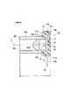
図6は従来の光ファイバーモジュールを示した縦断面図である。 FIG. 6 is a longitudinal sectional view showing a conventional optical fiber module.
図6に示した従来の光ファイバーモジュール100は、上記した特許文献1に開示されているものであり、ここでは特許文献1を参照して簡略に説明する。 The conventional optical fiber module 100 shown in FIG. 6 is disclosed in Patent Document 1 described above, and will be briefly described here with reference to Patent Document 1.
図6に示した如く、従来の光ファイバーモジュール100は、基板111の一側面111aに発光素子(又は、受光素子)112及び発光用IC(又は、受光用IC)113を取り付けた発光デバイス(又は、受光デバイス)110と、不図示の光ファイバーと結合し且つ基板111の一側面111a側に搭載されるハウジング120とを備えている。 As shown in FIG. 6, the conventional optical fiber module 100 includes a light emitting device (or a light receiving element) 112 and a light emitting IC (or light receiving IC) 113 attached to one
上記した発光デバイス110では、発光素子112として例えばLED(Light Emitting Diode)などを用いる一方、受光素子112として例えばPD(Phto Diode)などを用いており、発光素子112又は受光素子112のいずれか一方が基板111上に取り付けられている。 In the
また、ハウジング120は、不図示の光ファイバーを挿脱するための光通過孔120a1を内部に形成した円筒形状のスリーブ部120aと、発光デバイス(又は、受光デバイス)110を収納するための段付き凹部120b1を内部に形成した方形状の本体部120bとが互いに連接して一体的に形成されている。 The
また、ハウジング120の本体部120bの凹部120b1内には、基板111上に取り付けた発光素子(又は、受光素子)112及び発光用IC(又は、受光用IC)113を封止する封止樹脂121が充填されており、この封止樹脂121は透光性エポキシ樹脂などを用いている。 Further, a
そして、ハウジング120の本体部120bの凹部120b1内に発光デバイス(又は、受光デバイス)110を収納したときに、基板111上に取り付けた発光素子(又は、受光素子)112がハウジング120のスリーブ部120a内に形成した光通過孔120a1に対して光軸Kを合致させるように、本体部120b中で互いに対向する側壁に形成したフック部120b2を基板111の一側面111aとは反対側の他側面111bの上下に形成した切欠部111b1に係合させることで、光ファイバーモジュール100の組立工数を削減でき且つ低コスト化が可能である旨が記載されている。
ところで、上記した従来の光ファイバーモジュール100では、ハウジング120の本体部120bの凹部120b1内に発光デバイス(又は、受光デバイス)110を収納するために、本体部120bが発光デバイス(又は、受光デバイス)110よりも一回り大型な方形状に形成されているので、本体部120bが大型化してしまうと共に、方形状の本体部120bは金型代が高くなるので光ファイバーモジュール100の製品単価も高価になってしまう。 By the way, in the above-described conventional optical fiber module 100, the
また、ハウジング120の本体部120bの凹部120b1内に発光素子(又は、受光素子)112及び発光用IC(又は、受光用IC)113を封止する封止樹脂121を充填させるためのスペースが必要であり、このスペースを確保するために、本体部120bの凹部120b1内に光軸方向に沿って所定の長さL1の間隔を設定する必要があるので、光ファイバーモジュール100の全長Lが長くなってしまう。 Further, a space for filling the light emitting element (or light receiving element) 112 and the light emitting IC (or light receiving IC) 113 in the recess 120b1 of the
また、封止樹脂121は、発光素子(又は、受光素子)112に対して透光性の良い樹脂材を用いるために高価になると共に、封止樹脂121を硬化させるのに時間がかかり、組立性能が良好であるとは言えない。 Further, the
そこで、樹脂製基台の一側面側を臨むように発光素子又は受光素子のいずれか一方の光電変換素子が取り付けられた光電変換素子パッケージと、光ファイバーと結合するために樹脂製基台の一側面側に搭載される光ファイバー結合体とを備えて光通信モジュールを構成する際に、小型化が可能で全長を短く設定でき、且つ、製品単価が安価となると共に、光軸ズレが生じない性能の良い光通信モジュールが望まれている。 Therefore, a photoelectric conversion element package in which either one of the light emitting element and the light receiving element is attached so as to face one side of the resin base, and one side of the resin base for coupling with the optical fiber When configuring an optical communication module with an optical fiber assembly mounted on the side, the size can be reduced, the overall length can be set short, the unit price of the product is low, and the optical axis is not displaced. A good optical communication module is desired.
本発明は上記課題に鑑みてなされたものであり、第1の発明は、樹脂製基台の一側面側を臨むように発光素子又は受光素子のいずれか一方の光電変換素子が取り付けられた光電変換素子パッケージと、光ファイバーと結合するための光通過孔を円筒部内に有し、前記樹脂製基台の一側面側に搭載される光ファイバー結合体とを備え、前記光電変換素子と前記光ファイバー結合体内に形成した前記光通過孔とが光軸を合わせて組み立てられた光通信モジュールにおいて、
前記光電変換素子パッケージは、前記樹脂製基台の一側面と対向した他側面側に前記光電変換素子が取り付けられ、且つ、前記一側面と前記他側面との間に前記光軸に合わせて貫通して穿設された孔の中心位置に前記光電変換素子が配置されていることを特徴とする光通信モジュールである。The present invention has been made in view of the above problems, and the first invention is a photoelectric device in which either one of a light emitting element and a light receiving element is attached so as to face one side of a resin base. A conversion element package; and an optical fiber coupling body having a light passage hole for coupling with an optical fiber in a cylindrical portion and mounted on one side of the resin base, the photoelectric conversion element and the optical fiber coupling body In the optical communication module assembled with the optical passage and the optical passage hole formed in,
The photoelectric conversion element package has the photoelectric conversion element attached to the other side facing the one side of the resin base, and penetrates between the one side and the other side according to the optical axis. In this optical communication module, the photoelectric conversion element is disposed at the center position of the hole formed.
また、第2の発明は、上記した第1の発明の光通信モジュールにおいて、
前記光ファイバー結合体は、長尺で大径に形成し大径円筒部と、短尺で小径に形成した小径円筒部とを連接させて両筒部の内部に前記光通過孔を形成し、且つ、前記小径円筒部を前記樹脂製基台内に貫通して穿設した前記孔内に嵌合させたことを特徴とする光通信モジュールである。The second invention is the optical communication module of the first invention described above,
The optical fiber conjugate is formed to be long and large in diameter and connected to a large diameter cylindrical portion and a short and small diameter small cylindrical portion to form the light passage hole in both cylindrical portions, and The optical communication module is characterized in that the small-diameter cylindrical portion is fitted into the hole formed by penetrating through the resin base.
更に、第3の発明は、上記した第1又は第2の発明の光通信モジュールにおいて、
前記光ファイバー結合体は、前記光通過孔内に結像レンズを設けたことを特徴とする光通信モジュールである。Furthermore, a third invention is the optical communication module of the first or second invention described above,
The optical fiber coupled body is an optical communication module in which an imaging lens is provided in the light passage hole.
本発明に係る光通信モジュールによると、樹脂製基台の一側面側を臨むように発光素子又は受光素子のいずれか一方の光電変換素子が取り付けられた光電変換素子パッケージと、光ファイバーと結合するための光通過孔を円筒部内に有し、樹脂製基台の一側面側に搭載される光ファイバー結合体とを備え、光電変換素子と光ファイバー結合体内に形成した光通過孔とを光軸を合わせて組み立てた際に、とくに、光電変換素子パッケージは、樹脂製基台の一側面と対向した他側面側に光電変換素子が取り付けられ、且つ、一側面と他側面との間に光軸に合わせて貫通して穿設された孔の中心位置に光電変換素子が配置されているので、この結果、樹脂製基台の他側面側に取り付けた光電変換素子と、光ファイバー結合体内に形成した光通過孔とを光軸を合わせて位置精度良く組み立てることができ、光軸ズレが生じない性能の良い光通信モジュールを提供することができる。 According to the optical communication module according to the present invention, the photoelectric conversion element package to which either the light emitting element or the light receiving element is attached so as to face one side of the resin base is coupled to the optical fiber. The optical passage is formed in the cylindrical portion, and is provided on one side of the resin base with an optical fiber coupling body. The photoelectric conversion element and the light passage hole formed in the optical fiber coupling body are aligned with the optical axis. When assembled, in particular, in the photoelectric conversion element package, the photoelectric conversion element is attached to the other side facing the one side of the resin base, and the optical axis is aligned between the one side and the other side. Since the photoelectric conversion element is arranged at the center position of the hole drilled through, the photoelectric conversion element attached to the other side of the resin base and the light passage hole formed in the optical fiber coupling body. When Can be assembled high positional accuracy combined optical axis, it is possible to provide a optical communication module of performance optical axis misalignment does not occur.
また、光ファイバー結合体の小径円筒部を樹脂製基台に形成した位置決め用丸孔内に嵌合させる際に、光電変換素子の前方に従来例と異なって封止樹脂を充填するためのスペースが必要なく、且つ、光ファイバー結合体の外形が円筒状のみであるので光通信モジュールの小型化が可能で全長を短く設定でき、且つ、光ファイバー結合体の金型代が安いので光通信モジュールの製品単価が安価となる。 In addition, when the small-diameter cylindrical portion of the optical fiber coupled body is fitted into the positioning round hole formed on the resin base, there is a space for filling the sealing resin in front of the photoelectric conversion element unlike the conventional example. It is not necessary, and the outer shape of the optical fiber coupler is only cylindrical. Therefore, the optical communication module can be downsized, the overall length can be set short, and the mold cost of the optical fiber coupler is low. Is cheaper.
更に、光ファイバー結合体に形成した光通過孔内に結像レンズを設けることにより、電変換素子として発光素子を適用した場合に発光素子からの光を光ファイバーに良好に結像でき、一方、電変換素子として受光素子を適用した場合に光ファイバーからの光を受光素子に良好に結像できるので、信頼性の良い光通信を行うことができる。 Furthermore, by providing an imaging lens in the light passage hole formed in the optical fiber combination, when the light emitting element is applied as the electric conversion element, the light from the light emitting element can be imaged well on the optical fiber, while the electric conversion When a light receiving element is applied as the element, light from the optical fiber can be favorably imaged on the light receiving element, so that reliable optical communication can be performed.
以下に本発明に係る光通信モジュールの一実施例について図1〜図5を参照して詳細に説明する。 Hereinafter, an embodiment of an optical communication module according to the present invention will be described in detail with reference to FIGS.
図1は本発明に係る実施例の光通信モジュールを分解して示した分解斜視図、
図2は本発明に係る実施例の光通信モジュールを示した縦断面図、
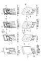
図3(a)〜(h)は図1及び図2示した光電変換素子パッケージを製造する工程を示した工程図である。FIG. 1 is an exploded perspective view showing an exploded optical communication module according to an embodiment of the present invention,
FIG. 2 is a longitudinal sectional view showing an optical communication module of an embodiment according to the present invention,
3A to 3H are process diagrams showing a process for manufacturing the photoelectric conversion element package shown in FIGS.
図1及び図2に示した如く、本発明に係る実施例の光通信モジュール1は、略直方体形状に形成した樹脂製基台11の一側面11a側を臨むように発光素子又は受光素子のいずれか一方の光電変換素子12が取り付けられた光電変換素子パッケージ10と、不図示の光ファイバーと結合するための光通過孔20cを円筒部20a,20b内に有し、樹脂製基台11の一側面11a側に搭載される光ファイバー結合体20とを備え、光電変換素子12と光ファイバー結合体20内の光通過孔20cとが光軸Kを合わせて組み立てられている。 As shown in FIGS. 1 and 2, the optical communication module 1 according to the embodiment of the present invention is either a light emitting element or a light receiving element so as to face one
この際、上記した光ファイバー結合体20は、樹脂製基台11の一側面11aと対向した他側面11b側に光電変換素子12が取り付けられ、且つ、一側面11aと他側面11bとの間に光軸Kに合わせて貫通して穿設された位置決め用丸孔11cの中心位置に光電変換素子12が配置されていることで、光通信モジュール1の小型化が可能になっている。 At this time, the above-described optical fiber combined
ここで、本発明に係る実施例の光通信モジュール1を構成する各構成部材について順を追って説明する。 Here, the constituent members constituting the optical communication module 1 of the embodiment according to the present invention will be described in order.
まず、実施例の光通信モジュール1の要部となる光電変換素子パッケージ10は、樹脂材を用いて樹脂製基台11が所定の厚みを持って略直方体形状に形成されており、一側面11aと所定の厚みを隔てて対向する他側面11b側に発光素子又は受光素子のうちいずれか一方の光電変換素子12が取り付けられている。 First, in a photoelectric
この実施例では、上記した光電変換素子12が円板状に形成された円板状配線基板13の基板中心位置に半田付けされており、且つ、円板状配線基板13は樹脂製基台11の他側面11bに固着されたリードフレーム14の一側面14a上に貼着されているので、光電変換素子12が円板状配線基板13及びリードフレーム14を介して樹脂製基台11の他側面11b側に取り付けられていることになる。 In this embodiment, the
また、樹脂製基台11は、一側面14aと他側面14bとの間に位置決め用丸孔11cが前記した光軸Kに合わせて貫通して穿設されており、この位置決め用丸孔11c内に光電変換素子12を基板中心位置に半田付けした円板状配線基板13が嵌合されているので、光電変換素子12が光軸Kに合わせて位置決め用丸孔11cの中心位置に配置されていることになる。 The
次に、上記した光電変換素子12は、前述したように、発光素子又は受光素子のいずれか一方が用いられているが、光電変換素子12として発光素子を適用した場合にこの発光素子は、発光ダイオード(LED:Light Emitting Diode)や垂直共振型面発光レーザー(VCSEL:Vertical Cavity Surface Emitting Laser)などが用いられている。一方、光電変換素子12として受光素子を適用した場合にこの受光素子は、フォトダイオード(PD:Phto Diode)が用いられている。 Next, as described above, either the light emitting element or the light receiving element is used for the
尚、この実施例では、光電変換素子12として発光素子の一種である垂直共振型面発光レーザー(VCSEL)を用いて、この垂直共振型面発光レーザー(VCSEL)を円板状配線基板13の中心位置に半田付けしている。 In this embodiment, a vertical cavity surface emitting laser (VCSEL), which is a kind of light emitting element, is used as the
次に、リードフレーム14は、導電性を有する銅板などの導電性板材を用いており、一側面14a及びこの側面14aと板厚を隔てて対向した他側面14bが共に平坦に形成され、且つ、一側面14aに上記した光電変換素子12を半田付けした円板状配線基板13が貼着され、一方、図2に示したように、他側面14bに表面実装部品(SMD:Surfe Mount Device)16及びIC集積回路部品(LSI:Latge Scale Integration)17を半田付けした矩形状配線基板15が貼着され、更に、下端側に延出形成したリード端子14cが樹脂製基台11の底面11dから複数本突出している。 Next, the
そして、矩形状配線基板15に半田付けされた表面実装部品(SMD)16上及びIC集積回路部品(LSI)17上に熱硬化性エポキシ樹脂などを用いてIC用封止樹脂18が充填されて両部品16,17を覆っている。 Then, the surface mounting component (SMD) 16 and the IC integrated circuit component (LSI) 17 soldered to the
ここで、本発明の要部となる光電変換素子パッケージ10の製造工程について図3(a)〜(h)を用いて簡略に説明する。 Here, a manufacturing process of the photoelectric
まず、図3(a)に示した如く、リードフレーム14を用意する。 First, as shown in FIG. 3A, a
次に、図3(b)に示した如く、リードフレーム14の一側面14aに円板状配線基板13を貼着すると共に、リードフレーム14の他側面14bに2枚の矩形状配線基板15を貼着する。 Next, as shown in FIG. 3B, the disc-
次に、図3(c)に示した如く、2枚の矩形状配線基板15上に複数の表面実装部品(SMD)16及びIC集積回路部品(LSI)17をそれぞれ搭載する。 Next, as shown in FIG. 3C, a plurality of surface mount components (SMD) 16 and IC integrated circuit components (LSI) 17 are mounted on two
次に、図3(d)に示した如く、複数の表面実装部品(SMD)16上及びIC集積回路部品(LSI)17をAuワイヤで2枚の矩形状配線基板15上にボンディングする。 Next, as shown in FIG. 3D, a plurality of surface mount components (SMD) 16 and IC integrated circuit components (LSI) 17 are bonded to two
次に、図3(e)に示した如く、リードフレーム14の一側面14a側にインサート成形により樹脂製基台11を成形し、且つ、複数の表面実装部品(SMD)16上及びIC集積回路部品(LSI)17上をIC用封止樹脂18で覆う。 Next, as shown in FIG. 3E, a
次に、図3(f)に示した如く、図3(e)の状態で全体を反転させる。 Next, as shown in FIG. 3F, the whole is reversed in the state of FIG.
次に、図3(g)に示した如く、樹脂製基台11の一側面11aと他側面11bとの間に貫通した位置決め用丸孔11c内に嵌合した円板状配線基板13上に光電変換素子12として発光素子の一種である垂直共振型面発光レーザー(VCSEL)を搭載する。 Next, as shown in FIG. 3G, on the disc-
次に、図3(h)に示した如く、垂直共振型面発光レーザー(VCSEL)12をAuワイヤで円板状配線基板13上にワイヤボンディングすると、光電変換素子パッケージ10が完成する。 Next, as shown in FIG. 3H, when the vertical cavity surface emitting laser (VCSEL) 12 is wire-bonded onto the disc-
上記のように製造された光電変換素子パッケージ10は、厚みが薄く小型に一体化されて、品質及び信頼性が良好なものとなる。 The photoelectric
再び、図1及び図2に戻り、樹脂製基台11の一側面11a側に搭載される光ファイバー結合体20は、光透過性のプラスチック(例えば、PEI,PC,PMMA等)を用いて長尺で大径の大径円筒部20aと短尺で小径の小径円筒部20bとが連接して段付き円筒形状に射出成形されており、且つ、且つ、不図示の光ファイバーを挿脱するための光通過孔20cが大径円筒部20aから小径円筒部20bに向かって形成されていると共に、この光通過孔20c内に結像レンズ20dが一体的に設けられている。 1 and 2 again, the optical fiber coupled
この際、光電変換素子12として発光素子を適用した場合に、光ファイバー結合体20内に一体形成した結像レンズ20dは、発光素子と対向する側が平坦面に形成され、且つ、この平坦面に入射した発光素子からの光を出射する側が凸曲面に形成されている。 At this time, when a light emitting element is applied as the
尚、光電変換素子12として受光素子を適用した場合に、光ファイバー結合体20内に一体形成した結像レンズ20dは、上記とは逆に不図示の凸曲面側を受光素子と対向するように形成すれば良いものである。 When a light receiving element is applied as the
上記のように、光ファイバー結合体20に形成した光通過孔20c内に結像レンズ20dを設けることにより、電変換素子12として発光素子を適用した場合に発光素子からの光を不図示の光ファイバーに良好に結像でき、一方、電変換素子12として受光素子を適用した場合に不図示の光ファイバーからの光を受光素子に良好に結像できるので、信頼性の良い光通信を行うことができる。 As described above, by providing the
また、光ファイバー結合体20に形成した大径円筒部20aは、不図示の光ファイバーを挿脱する側に配置されている。一方、光ファイバー結合体20に形成した小径円筒部20bは、樹脂製基台11の一側面11aと他側面11bとの間に貫通して穿設された位置決め用丸孔11c内に嵌合されて不図示の接着剤を用いて固着されている。 The large-diameter
これにより、樹脂製基台11の他側面11b側に取り付けた光電変換素子12と、光ファイバー結合体20内に形成した光通過孔20c及び結像レンズ20dとを光軸Kを合わせて位置精度良く組み立てることができ、光軸ズレが生じない性能の良い光通信モジュール1を提供することができる。 Thereby, the
また、光ファイバー結合体20の小径円筒部20bを樹脂製基台11内に形成した位置決め用丸孔11c内に嵌合させる際に、光電変換素子12の前方に従来例と異なって封止樹脂を充填するためのスペースが必要なく、且つ、光ファイバー結合体20の外形が円筒状のみであるので光通信モジュール1の小型化が可能で全長L(図2)を短く設定でき、且つ、光ファイバー結合体20の金型代が安いので光通信モジュール1の製品単価が安価となる。 Further, when the small-diameter
次に、本発明に係る実施例の光通信モジュールを一部変形させた変形例の光通信モジュールについて図4及び図5を用いて簡略に説明する。 Next, a modified optical communication module obtained by partially modifying the optical communication module according to the embodiment of the present invention will be briefly described with reference to FIGS.
図4は本発明に係る実施例の光通信モジュールを一部変形させた変形例の光通信モジュールを分解して示した分解斜視図、
図5は本発明に係る実施例の光通信モジュールを一部変形させた変形例の光通信モジュールを示した縦断面図である。FIG. 4 is an exploded perspective view showing an exploded optical communication module of a modified example in which the optical communication module of the embodiment according to the present invention is partially deformed,
FIG. 5 is a longitudinal sectional view showing a modified optical communication module obtained by partially modifying the optical communication module of the embodiment according to the present invention.
図4及び図5に示した変形例の光通信モジュール1’は、先に図1及び図2を用いて説明した実施例1の光通信モジュール1の構成に対して光ファイバー結合体20’内の形状が一部異なるだけであり、ここでは説明の便宜上、先に示した構成部材に対しては同一の符号を付して図示し詳細な説明を省略するものの、実施例に対して異なる点を中心にして簡略に説明する。 The optical communication module 1 ′ of the modified example shown in FIGS. 4 and 5 is provided in the optical fiber combined
図4及び図5に示した如く、実施例を一部変形させた変形例の光通信モジュール1’も、実施例と略同様に、略直方体形状に形成した樹脂製基台11の一側面11a側を臨むように発光素子又は受光素子のいずれか一方の光電変換素子12が取り付けられた光電変換素子パッケージ10と、不図示の光ファイバーと結合するための光通過孔20cを円筒部20a,20b内に有し、樹脂製基台11の一側面11a側に搭載される光ファイバー結合体20’とを備え、光電変換素子12と光ファイバー結合体20’内の光通過孔20cとが光軸Kを合わせて組み立てられている。 As shown in FIGS. 4 and 5, an optical communication module 1 ′, which is a modified example of a part of the embodiment, is also provided on one
この際、上記した光ファイバー結合体20’は、樹脂製基台11の一側面11aと対向した他側面11b側に光電変換素子12が取り付けられ、且つ、一側面11aと他側面11bとの間に光軸Kに合わせて貫通して穿設された位置決め用丸孔11cの中心位置に光電変換素子12が配置されていることで、変形例の光通信モジュール1’の小型化が可能になっている点は実施例と同じである。 At this time, the above-described optical fiber combined
ここで、実施例1に対して異なる点は、円筒形状の光ファイバー結合体20’内に光通過孔20cが大径円筒部20aと小径円筒部20bとの間で貫通して穿設されており、この光通過孔20c内に結合レンズを設けないことで、光ファイバー結合体20’の簡素化を図ったことである。 Here, the difference from the first embodiment is that a
これにより、光ファイバー結合体20’は実施例のような光透過性の良い樹脂材を用いることなく、既存の安価な樹脂材を用いることができ、更に、結合レンズを設けないぶんだけ金型代が安くなり、実施例よりもより一層安価で簡単に使用できる変形例の光通信モジュール1’を提供することができる。 As a result, the optical fiber coupled body 20 'can be made of an existing inexpensive resin material without using a resin material having a good light transmission as in the embodiment, and moreover, the mold cost is not increased as long as no coupling lens is provided. Therefore, it is possible to provide a modified optical communication module 1 ′ that is much cheaper and easier to use than the embodiment.
1…実施例の光通信モジュール、
1’…実施例を一部変形させた変形例の光通信モジュール1、
10…光電変換素子パッケージ、
11…樹脂製基台、
11a…一側面、11b…他側面、11c…位置決め用丸孔、11d…底面、
12…光電変換素子、13…円板状配線基板、
14…リードフレーム、14a…一側面、14b…他側面、14c…リード端子、
15…矩形状配線基板、16…表面実装部品(SMD)、
17…IC集積回路部品(LSI)、18…IC用封止樹脂、
20…光ファイバー結合体、
20’…実施例を一部変形させた光ファイバー結合体、
20a…大径円筒部、20b…小径円筒部、
20c…光通過孔、20d…結像レンズ、
K…光軸。1 ... Optical communication module of embodiment,
1 ′: a modified optical communication module 1 in which the embodiment is partially modified,
10: photoelectric conversion element package,
11 ... resin base,
11a ... one side surface, 11b ... other side surface, 11c ... round hole for positioning, 11d ... bottom surface,
12 ... photoelectric conversion element, 13 ... disk-shaped wiring board,
14 ... Lead frame, 14a ... One side surface, 14b ... Other side surface, 14c ... Lead terminal,
15 ... rectangular wiring board, 16 ... surface mount component (SMD),
17 ... IC integrated circuit parts (LSI), 18 ... IC sealing resin,
20 ... optical fiber combination,
20 ′: an optical fiber combination obtained by partially modifying the embodiment,
20a ... large diameter cylindrical part, 20b ... small diameter cylindrical part,
20c ... light passage hole, 20d ... imaging lens,
K: Optical axis.
Claims (3)
Translated fromJapanese前記光電変換素子パッケージは、前記樹脂製基台の一側面と対向した他側面側に前記光電変換素子が取り付けられ、且つ、前記一側面と前記他側面との間に前記光軸に合わせて貫通して穿設された孔の中心位置に前記光電変換素子が配置されていることを特徴とする光通信モジュール。The cylindrical part has a photoelectric conversion element package to which either one of the light emitting element and the light receiving element is attached so as to face one side of the resin base, and a light passage hole for coupling with the optical fiber. And an optical communication module mounted on one side of the resin base, wherein the photoelectric conversion element and the light passage hole formed in the optical fiber combination are assembled with their optical axes aligned. In
The photoelectric conversion element package has the photoelectric conversion element attached to the other side facing the one side of the resin base, and penetrates between the one side and the other side according to the optical axis. An optical communication module, wherein the photoelectric conversion element is disposed at a center position of the hole formed in the hole.
Priority Applications (6)
| Application Number | Priority Date | Filing Date | Title |
|---|---|---|---|
| JP2008101809AJP2009253166A (en) | 2008-04-09 | 2008-04-09 | Optical communication module |
| US12/937,001US8608390B2 (en) | 2008-04-09 | 2008-12-09 | Optical communication module |
| CN2008801285218ACN101999088B (en) | 2008-04-09 | 2008-12-09 | Optical communication module |
| EP08873825AEP2277069A1 (en) | 2008-04-09 | 2008-12-09 | Optical communication module |
| PCT/JP2008/003662WO2009125455A1 (en) | 2008-04-09 | 2008-12-09 | Optical communication module |
| KR1020107023520AKR20100133444A (en) | 2008-04-09 | 2008-12-09 | Optical communication module |
Applications Claiming Priority (1)
| Application Number | Priority Date | Filing Date | Title |
|---|---|---|---|
| JP2008101809AJP2009253166A (en) | 2008-04-09 | 2008-04-09 | Optical communication module |
Publications (1)
| Publication Number | Publication Date |
|---|---|
| JP2009253166Atrue JP2009253166A (en) | 2009-10-29 |
Family
ID=40419085
Family Applications (1)
| Application Number | Title | Priority Date | Filing Date |
|---|---|---|---|
| JP2008101809AAbandonedJP2009253166A (en) | 2008-04-09 | 2008-04-09 | Optical communication module |
Country Status (6)
| Country | Link |
|---|---|
| US (1) | US8608390B2 (en) |
| EP (1) | EP2277069A1 (en) |
| JP (1) | JP2009253166A (en) |
| KR (1) | KR20100133444A (en) |
| CN (1) | CN101999088B (en) |
| WO (1) | WO2009125455A1 (en) |
Cited By (3)
| Publication number | Priority date | Publication date | Assignee | Title |
|---|---|---|---|---|
| KR101119950B1 (en)* | 2010-09-28 | 2012-03-16 | 경북대학교 산학협력단 | Light-emitting diode package having narrow emitting angle |
| CN104730654A (en)* | 2015-03-26 | 2015-06-24 | 厦门大学 | Optical transceiver chip packaging structure used for plastic optical fiber communication |
| JP2015175904A (en)* | 2014-03-13 | 2015-10-05 | オリンパス株式会社 | Optical transmission module and method for manufacturing the optical transmission module |
Families Citing this family (10)
| Publication number | Priority date | Publication date | Assignee | Title |
|---|---|---|---|---|
| US9116262B2 (en) | 2010-04-20 | 2015-08-25 | The Johns Hopkins University | High-efficiency illumination system |
| KR101434395B1 (en)* | 2011-09-21 | 2014-09-02 | 한국전자통신연구원 | Bidirectional optical transmitting and receiving device |
| CN103282814B (en) | 2011-12-26 | 2015-02-25 | 株式会社藤仓 | Optical module |
| JP6005362B2 (en)* | 2012-01-19 | 2016-10-12 | 日本航空電子工業株式会社 | Optical module and optical transmission module |
| TWI560481B (en)* | 2012-10-29 | 2016-12-01 | Hon Hai Prec Ind Co Ltd | Photoelectric converting module |
| TW201441704A (en)* | 2013-04-17 | 2014-11-01 | Hon Hai Prec Ind Co Ltd | Optical communication module |
| US9733440B2 (en)* | 2014-04-29 | 2017-08-15 | Corning Incorporated | Optical connectors for coupling light sources to optical fibers |
| EP3174088B1 (en)* | 2015-11-26 | 2020-12-30 | Siyang Grande Electronics Co., Ltd. | Method of manufacturing a plastic packaged smd diode |
| CN110568571A (en)* | 2019-10-24 | 2019-12-13 | 刘向宁 | A passive optical fiber conversion device |
| CN113467015B (en)* | 2021-08-03 | 2023-03-21 | 新疆师范大学 | Center calibrating device of laser coupling platform |
Citations (6)
| Publication number | Priority date | Publication date | Assignee | Title |
|---|---|---|---|---|
| JPH05267694A (en)* | 1992-03-19 | 1993-10-15 | Nec Corp | Photoelectric conversion device |
| JP2000277814A (en)* | 1999-03-29 | 2000-10-06 | Sumitomo Electric Ind Ltd | Optical communication module |
| JP2002023025A (en)* | 2000-07-07 | 2002-01-23 | Yazaki Corp | Optical connector |
| JP2002082258A (en)* | 2000-07-03 | 2002-03-22 | Yazaki Corp | Hybrid connector assembling method and hybrid connector |
| JP2004138966A (en)* | 2002-10-21 | 2004-05-13 | Yazaki Corp | Single-core bidirectional optical transceiver |
| JP2007086177A (en)* | 2005-09-20 | 2007-04-05 | Yazaki Corp | Light emitting / receiving device measuring device |
Family Cites Families (10)
| Publication number | Priority date | Publication date | Assignee | Title |
|---|---|---|---|---|
| DE3172553D1 (en)* | 1980-11-28 | 1985-11-07 | Toshiba Kk | Method for manufacturing a module for a fiber optic link |
| IT1169922B (en)* | 1983-11-04 | 1987-06-03 | Telettra Lab Telefon | SYSTEM AND DEVICES FOR CONNECTING DETECTORS AND FIBER OPTICS |
| JPH02275913A (en) | 1989-04-18 | 1990-11-09 | Sumitomo Electric Ind Ltd | Optical receptacle |
| JP2941303B2 (en) | 1989-05-12 | 1999-08-25 | 株式会社日立製作所 | Optical front-end device |
| EP0826997B1 (en)* | 1996-08-26 | 2003-07-23 | Sumitomo Electric Industries, Ltd. | Optoelectronic module and method of manufacturing the same |
| JP3979168B2 (en)* | 2002-04-26 | 2007-09-19 | ヤマハ株式会社 | Light emitting part structure in a key depression detection device for a keyboard instrument |
| JP2004334023A (en) | 2003-05-09 | 2004-11-25 | Fujikura Ltd | Optical module and photocatalyst device |
| JP2006030813A (en) | 2004-07-21 | 2006-02-02 | Citizen Electronics Co Ltd | Optical fiber module |
| US7223028B2 (en)* | 2004-09-09 | 2007-05-29 | Finisar Corporation | Optical barrels with electromagnetic shielding |
| JP3955065B2 (en) | 2005-01-18 | 2007-08-08 | シャープ株式会社 | Optical coupler |
- 2008
- 2008-04-09JPJP2008101809Apatent/JP2009253166A/ennot_activeAbandoned
- 2008-12-09KRKR1020107023520Apatent/KR20100133444A/ennot_activeCeased
- 2008-12-09WOPCT/JP2008/003662patent/WO2009125455A1/enactiveApplication Filing
- 2008-12-09EPEP08873825Apatent/EP2277069A1/ennot_activeWithdrawn
- 2008-12-09USUS12/937,001patent/US8608390B2/enactiveActive
- 2008-12-09CNCN2008801285218Apatent/CN101999088B/ennot_activeExpired - Fee Related
Patent Citations (6)
| Publication number | Priority date | Publication date | Assignee | Title |
|---|---|---|---|---|
| JPH05267694A (en)* | 1992-03-19 | 1993-10-15 | Nec Corp | Photoelectric conversion device |
| JP2000277814A (en)* | 1999-03-29 | 2000-10-06 | Sumitomo Electric Ind Ltd | Optical communication module |
| JP2002082258A (en)* | 2000-07-03 | 2002-03-22 | Yazaki Corp | Hybrid connector assembling method and hybrid connector |
| JP2002023025A (en)* | 2000-07-07 | 2002-01-23 | Yazaki Corp | Optical connector |
| JP2004138966A (en)* | 2002-10-21 | 2004-05-13 | Yazaki Corp | Single-core bidirectional optical transceiver |
| JP2007086177A (en)* | 2005-09-20 | 2007-04-05 | Yazaki Corp | Light emitting / receiving device measuring device |
Cited By (3)
| Publication number | Priority date | Publication date | Assignee | Title |
|---|---|---|---|---|
| KR101119950B1 (en)* | 2010-09-28 | 2012-03-16 | 경북대학교 산학협력단 | Light-emitting diode package having narrow emitting angle |
| JP2015175904A (en)* | 2014-03-13 | 2015-10-05 | オリンパス株式会社 | Optical transmission module and method for manufacturing the optical transmission module |
| CN104730654A (en)* | 2015-03-26 | 2015-06-24 | 厦门大学 | Optical transceiver chip packaging structure used for plastic optical fiber communication |
Also Published As
| Publication number | Publication date |
|---|---|
| US20110026937A1 (en) | 2011-02-03 |
| KR20100133444A (en) | 2010-12-21 |
| EP2277069A1 (en) | 2011-01-26 |
| CN101999088A (en) | 2011-03-30 |
| WO2009125455A1 (en) | 2009-10-15 |
| CN101999088B (en) | 2013-03-06 |
| US8608390B2 (en) | 2013-12-17 |
Similar Documents
| Publication | Publication Date | Title |
|---|---|---|
| JP2009253166A (en) | Optical communication module | |
| JP5246136B2 (en) | Optical transceiver | |
| CN110568569A (en) | integrated packaged optical engine and signal transmitting and receiving method thereof | |
| CN101569023A (en) | Housing for an optoelectronic component and arrangement of the optoelectronic component in the housing | |
| CN100578764C (en) | Optical semiconductor devices, optical connectors, and electronic equipment | |
| JP4269291B2 (en) | Optical module | |
| JP2009260227A (en) | Photoelectric conversion device | |
| JP2010237640A (en) | Optical module and cable with module | |
| US7850374B2 (en) | Optical transmitter module with an integrated lens and method for making the module | |
| US7220063B2 (en) | Optical transceiver module | |
| JP2006030716A (en) | Surface mounting type module | |
| JP2003008065A (en) | Method for manufacturing smd type optical element module | |
| JP5956815B2 (en) | Optical module substrate and optical module | |
| JP2003241028A (en) | Optical transmission module | |
| WO2010146962A1 (en) | Optical communication module | |
| JP2008109048A (en) | Optical semiconductor device and optical transmission device | |
| JP5402786B2 (en) | Manufacturing method of optical communication module | |
| JP4852517B2 (en) | Optical transceiver | |
| JPH0935594A (en) | Photosensor | |
| TWI231108B (en) | Optical transceiver module and manufacturing method thereof | |
| JP2011197275A (en) | Optical link module | |
| JP2008003168A (en) | Optical module | |
| JP2007266309A (en) | Optical coupling element | |
| JP2013020080A (en) | Optical module and manufacturing method of the same | |
| JP2005233995A (en) | Manufacturing method of photoelectric conversion plug |
Legal Events
| Date | Code | Title | Description |
|---|---|---|---|
| A621 | Written request for application examination | Free format text:JAPANESE INTERMEDIATE CODE: A621 Effective date:20110225 | |
| A131 | Notification of reasons for refusal | Free format text:JAPANESE INTERMEDIATE CODE: A131 Effective date:20130416 | |
| A977 | Report on retrieval | Free format text:JAPANESE INTERMEDIATE CODE: A971007 Effective date:20130417 | |
| A521 | Request for written amendment filed | Free format text:JAPANESE INTERMEDIATE CODE: A523 Effective date:20130612 | |
| A02 | Decision of refusal | Free format text:JAPANESE INTERMEDIATE CODE: A02 Effective date:20130903 | |
| A521 | Request for written amendment filed | Free format text:JAPANESE INTERMEDIATE CODE: A523 Effective date:20131107 | |
| A911 | Transfer to examiner for re-examination before appeal (zenchi) | Free format text:JAPANESE INTERMEDIATE CODE: A911 Effective date:20131114 | |
| A912 | Re-examination (zenchi) completed and case transferred to appeal board | Free format text:JAPANESE INTERMEDIATE CODE: A912 Effective date:20131129 | |
| A762 | Written abandonment of application | Free format text:JAPANESE INTERMEDIATE CODE: A762 Effective date:20141003 |