JP2009244861A - Image display apparatus - Google Patents
Image display apparatusDownload PDFInfo
- Publication number
- JP2009244861A JP2009244861AJP2009049343AJP2009049343AJP2009244861AJP 2009244861 AJP2009244861 AJP 2009244861AJP 2009049343 AJP2009049343 AJP 2009049343AJP 2009049343 AJP2009049343 AJP 2009049343AJP 2009244861 AJP2009244861 AJP 2009244861A
- Authority
- JP
- Japan
- Prior art keywords
- guide plate
- light guide
- led element
- light
- image display
- Prior art date
- Legal status (The legal status is an assumption and is not a legal conclusion. Google has not performed a legal analysis and makes no representation as to the accuracy of the status listed.)
- Pending
Links
Images


Classifications
- G—PHYSICS
- G02—OPTICS
- G02B—OPTICAL ELEMENTS, SYSTEMS OR APPARATUS
- G02B6/00—Light guides; Structural details of arrangements comprising light guides and other optical elements, e.g. couplings
- G02B6/0001—Light guides; Structural details of arrangements comprising light guides and other optical elements, e.g. couplings specially adapted for lighting devices or systems
- G02B6/0011—Light guides; Structural details of arrangements comprising light guides and other optical elements, e.g. couplings specially adapted for lighting devices or systems the light guides being planar or of plate-like form
- G02B6/0081—Mechanical or electrical aspects of the light guide and light source in the lighting device peculiar to the adaptation to planar light guides, e.g. concerning packaging
- G02B6/0086—Positioning aspects
- G02B6/0091—Positioning aspects of the light source relative to the light guide
- G—PHYSICS
- G02—OPTICS
- G02B—OPTICAL ELEMENTS, SYSTEMS OR APPARATUS
- G02B6/00—Light guides; Structural details of arrangements comprising light guides and other optical elements, e.g. couplings
- G02B6/0001—Light guides; Structural details of arrangements comprising light guides and other optical elements, e.g. couplings specially adapted for lighting devices or systems
- G02B6/0011—Light guides; Structural details of arrangements comprising light guides and other optical elements, e.g. couplings specially adapted for lighting devices or systems the light guides being planar or of plate-like form
- G02B6/0033—Means for improving the coupling-out of light from the light guide
- G02B6/0035—Means for improving the coupling-out of light from the light guide provided on the surface of the light guide or in the bulk of it
- G02B6/004—Scattering dots or dot-like elements, e.g. microbeads, scattering particles, nanoparticles
- G02B6/0041—Scattering dots or dot-like elements, e.g. microbeads, scattering particles, nanoparticles provided in the bulk of the light guide
- G—PHYSICS
- G02—OPTICS
- G02B—OPTICAL ELEMENTS, SYSTEMS OR APPARATUS
- G02B6/00—Light guides; Structural details of arrangements comprising light guides and other optical elements, e.g. couplings
- G02B6/0001—Light guides; Structural details of arrangements comprising light guides and other optical elements, e.g. couplings specially adapted for lighting devices or systems
- G02B6/0011—Light guides; Structural details of arrangements comprising light guides and other optical elements, e.g. couplings specially adapted for lighting devices or systems the light guides being planar or of plate-like form
- G02B6/0033—Means for improving the coupling-out of light from the light guide
- G02B6/005—Means for improving the coupling-out of light from the light guide provided by one optical element, or plurality thereof, placed on the light output side of the light guide
- G02B6/0053—Prismatic sheet or layer; Brightness enhancement element, sheet or layer
- G—PHYSICS
- G02—OPTICS
- G02B—OPTICAL ELEMENTS, SYSTEMS OR APPARATUS
- G02B6/00—Light guides; Structural details of arrangements comprising light guides and other optical elements, e.g. couplings
- G02B6/0001—Light guides; Structural details of arrangements comprising light guides and other optical elements, e.g. couplings specially adapted for lighting devices or systems
- G02B6/0011—Light guides; Structural details of arrangements comprising light guides and other optical elements, e.g. couplings specially adapted for lighting devices or systems the light guides being planar or of plate-like form
- G02B6/0081—Mechanical or electrical aspects of the light guide and light source in the lighting device peculiar to the adaptation to planar light guides, e.g. concerning packaging
- G02B6/0085—Means for removing heat created by the light source from the package
Landscapes
- Physics & Mathematics (AREA)
- General Physics & Mathematics (AREA)
- Optics & Photonics (AREA)
- Liquid Crystal (AREA)
- Planar Illumination Modules (AREA)
Abstract
Translated fromJapaneseDescription
Translated fromJapanese本発明は、バックライト光源を備えた画像表示装置に関するものであり、特に、バックライト光源としてLED素子を備えた画像表示装置に関する。 The present invention relates to an image display device including a backlight light source, and more particularly to an image display device including an LED element as a backlight light source.
近年の画像表示装置では、液晶を用いたものが主流であり、ガラス上にTFTを形成し液晶を封じ込んだ液晶パネルに対し、その背面に設置されたバックライトから照射された光を透過させて画像を表示している。それ故、明るく美しい高品質画像を得ようとすると、バックライトは明るく、且つ、面上で均一でなければならない。 In the recent image display devices, those using liquid crystals are the mainstream, and light irradiated from the backlight installed on the back is transmitted to the liquid crystal panel in which the TFT is formed on the glass and the liquid crystal is sealed. The image is displayed. Therefore, in order to obtain a bright and beautiful high quality image, the backlight must be bright and uniform on the surface.
従来、このような液晶パネルを用いた画像表示装置のバックライトの光源には、冷陰極管が用いられて来たが、近年の技術的な進歩によってLED素子の効率と輝度が著しく向上し、冷陰極管並の効率と輝度が得られるようになってきた。そのために、特に、小型の液晶表示装置のバックライト光源としてLED素子が用いられるようになってきた。 Conventionally, a cold cathode tube has been used as a light source of a backlight of an image display device using such a liquid crystal panel, but the efficiency and brightness of the LED element has been remarkably improved by recent technical progress, Efficiency and brightness comparable to those of cold cathode tubes have been obtained. For this reason, in particular, LED elements have come to be used as backlight light sources for small liquid crystal display devices.
しかしながら、冷陰極が線状に発光するのに対して、LED素子の場合は点状に発光する。そのために、バックライト光源としてLED素子を用いる場合、冷陰極管と同等の照度を得ようとすると、低出力のLED素子を多数用いるか、もしくは高出力のLED素子を用いて光の分散を効率的に行う必要がある。 However, the cold cathode emits light in a linear manner, whereas the LED element emits light in a dot manner. Therefore, when using an LED element as a backlight light source, when trying to obtain an illuminance equivalent to that of a cold cathode tube, a large number of low-output LED elements are used, or high-power LED elements are used to efficiently distribute light. Need to be done.
このような、点光源としてのLED素子をバックライト光源として用いる例が多く開示されており、特に発光面の光度分布を均一にする例(例えば、特許文献1、2参照。)や、LED素子からの発生熱を放熱させて温度上昇を抑える例(例えば、特許文献3参照。)などが開示されている。 Many examples of using such an LED element as a point light source as a backlight light source have been disclosed. Particularly, an example in which the luminous intensity distribution on the light emitting surface is made uniform (see, for example,
しかしながら、近年、光源としてのLED素子は小型化と高出力化が進展している。一方で、これらの画像表示装置を用いた情報処理装置なども小型化あるいは携帯化が進み、外部での使用などに際しての耐衝撃性、耐振動性や、屋内、屋外でも使用可能なように、輝度のダイナミックレンジの広がりなどが要求されてきている。 However, in recent years, LED elements as light sources have been reduced in size and output. On the other hand, information processing devices using these image display devices are also becoming smaller or more portable, so that they can be used indoors and outdoors, as well as shock resistance and vibration resistance when used outside. The expansion of the dynamic range of luminance has been demanded.
耐衝撃性や耐振動性を確保するためには、バックライト光源部を構成する導光板として、従来のように厚みを厚くして剛性を高めることや、現行の冷陰極管を用いたバックライト光源部の基本構造を用いることなどが要求される。一方で、このような条件で、小型のLED素子を導光板の中間面とLED素子の中心軸とを合致させるために、LED素子基板に段差部を設けると、段差部によって放熱が阻害されるなどの課題が発生する。 In order to ensure impact resistance and vibration resistance, the light guide plate that makes up the backlight light source section can be made thicker and more rigid as in the past, or a backlight using current cold cathode tubes. It is required to use the basic structure of the light source unit. On the other hand, if a step portion is provided on the LED element substrate in order to match the intermediate surface of the light guide plate and the central axis of the LED element in a small LED element under such conditions, heat dissipation is hindered by the step portion. Problems such as occur.
そこで、本発明の目的は、このような課題を解決して、輝度の調節が可能で、且つ、高輝度を実現し、光度分布が均一で長寿命の画像表示装置を提供することである。 Accordingly, an object of the present invention is to solve such problems and provide an image display device that can adjust the luminance, achieve high luminance, have a uniform light intensity distribution, and have a long lifetime.
上記の目的を達成するために、本発明に係る画像表示装置は、液晶表示部と、
前記液晶表示部の表示面と相対する裏面に面して設けられ、前面で前記液晶表示部の裏面に面すると共に、前記前面と対向する底面に反射シートを有し、前記前面及び前記底面と垂直な側端面から入射した光を前記底面の前記反射シートで反射して前記前面側に導く導光板と、
前記導光板の前記側端面に対向する発光面から前記側端面に対して光照射するLED素子と、
を備え、
前記LED素子は、前記導光板の前記前面と前記底面との間の中間面を含む平面に対して、前記LED素子の発光面の中心軸が、前記導光板の前記底面側又は前記前面側のいずれかにずれて配置されている。In order to achieve the above object, an image display device according to the present invention includes a liquid crystal display unit,
The liquid crystal display unit is provided so as to face the back surface facing the display surface, faces the back surface of the liquid crystal display unit on the front surface, and has a reflection sheet on the bottom surface facing the front surface, the front surface and the bottom surface, A light guide plate that reflects light incident from a vertical side end surface by the reflection sheet on the bottom surface and guides the light to the front surface side;
An LED element that emits light to the side end surface from a light emitting surface facing the side end surface of the light guide plate;
With
The LED element has a central axis of the light emitting surface of the LED element on the bottom surface side or the front surface side of the light guide plate with respect to a plane including an intermediate surface between the front surface and the bottom surface of the light guide plate. It is arranged so as to be shifted to either.
上記の構成によれば、厚みを有して剛性を有する導光板を用いて耐衝撃性、耐振動性を有する画像表示装置を実現することができる。 According to said structure, the image display apparatus which has impact resistance and vibration resistance is realizable using the light-guide plate which has thickness and rigidity.
また、前記LED素子は、前記導光板の前記前面と前記底面との間の中間面を含む平面に対して、前記LED素子の発光面の前記導光板の厚さ方向の両端部が、前記導光板の前記底面側に含まれるように配置されていてもよい。 In addition, the LED element is configured such that both ends of the light emitting surface of the LED element in the thickness direction of the light guide plate are in the guide direction with respect to a plane including an intermediate surface between the front surface and the bottom surface of the light guide plate. You may arrange | position so that it may be contained in the said bottom face side of an optical plate.
上記の構成によれば、LED素子の光照射の中心軸と反射シートとの距離が短くなっているために、導光板の端部において、反射シートで反射して導光板から射出される光と導光板を通過する光との間隔が短くなり、液晶パネル部に均一に光を入射させるための導光板端部領域長さを短くすることができる。そのため、画像表示装置の額縁部を小さくし画像表示装置として全体に小さくすることができる。 According to the above configuration, since the distance between the central axis of the light irradiation of the LED element and the reflection sheet is short, the light reflected from the reflection sheet and emitted from the light guide plate at the end of the light guide plate The interval with the light passing through the light guide plate is shortened, and the length of the light guide plate end region for allowing light to uniformly enter the liquid crystal panel portion can be shortened. For this reason, the frame portion of the image display device can be made smaller and the entire image display device can be made smaller.
さらに、前記LED素子は、前記導光板の前記前面と前記底面との間の中間面を含む平面に対して、前記LED素子の発光面の前記導光板の厚さ方向の両端部が、前記導光板の前記前面側に含まれるように配置されていてもよい。 Further, the LED element has both ends of the light emitting surface of the LED element in the thickness direction of the light guide plate with respect to a plane including an intermediate surface between the front surface and the bottom surface of the light guide plate. You may arrange | position so that it may be contained in the said front side of an optical plate.
またさらに、前記LED素子は、
前記導光板の前記前面と前記底面との間の中間面を含む平面に対して、前記LED素子の発光面の前記導光板の厚さ方向の両端部が、前記導光板の前記前面側に含まれるように配置された上段LED素子と、
前記導光板の前記前面と前記底面との間の中間面を含む平面に対して、前記LED素子の発光面の前記導光板の厚さ方向の両端部が、前記導光板の前記底面側に含まれるように配置された下段LED素子と、
を有してもよい。Furthermore, the LED element is
Both ends of the light emitting surface of the LED element in the thickness direction of the light guide plate are included on the front side of the light guide plate with respect to a plane including an intermediate surface between the front surface and the bottom surface of the light guide plate. An upper LED element arranged to be
Both ends of the light emitting surface of the LED element in the thickness direction of the light guide plate are included on the bottom surface side of the light guide plate with respect to a plane including an intermediate surface between the front surface and the bottom surface of the light guide plate. Lower LED elements arranged to be
You may have.
上記の構成によれば、LED素子を多数配置することができる。また、それぞれのLED素子への入力を制御して、輝度の調節が可能で、且つ、高輝度を実現する画像表示装置を提供できる。 According to said structure, many LED elements can be arrange | positioned. Further, it is possible to provide an image display device that can adjust the luminance by controlling the input to each LED element and realize high luminance.
また、前記導光板の厚さ方向からみて、前記上段LED素子と、前記下段LED素子とは、交互に配置されていてもよい。 Further, when viewed from the thickness direction of the light guide plate, the upper LED elements and the lower LED elements may be alternately arranged.
上記の構成によれば、上段LED素子と下段LED素子とのそれぞれのLED素子から出射される光によって端部に発生する光の重畳による明暗現象を解消し、均一な光度分布の画像表示装置を実現することができる。 According to the above configuration, the light and dark phenomenon due to the superimposition of the light generated at the end by the light emitted from the LED elements of the upper LED element and the lower LED element is eliminated, and the image display device having a uniform luminous intensity distribution is obtained. Can be realized.
さらに、前記導光板の前記側端面に向かって開口する開口部を有する放熱板をさらに備えてもよい。この場合、前記上段LED素子と前記下段LED素子とは、前記放熱板の前記開口部に配置されていることが好ましい。 Furthermore, you may further provide the heat sink which has an opening part opened toward the said side end surface of the said light-guide plate. In this case, it is preferable that the upper LED element and the lower LED element are arranged in the opening of the heat sink.
上記の構成によれば、上段LED素子と下段LED素子とのそれぞれのLED素子から発生する熱を効果的に放熱させることができ、各LED素子への入力を容易に制御できる。 According to said structure, the heat which generate | occur | produces from each LED element of an upper stage LED element and a lower stage LED element can be thermally radiated effectively, and the input to each LED element can be controlled easily.
またさらに、前記導光板は、分散配置された前方散乱粒子を含んでもよい。 Still further, the light guide plate may include forward scattered particles dispersedly arranged.
また、前記導光板は、前記液晶表示部の裏面と対向する前記前面側の間にプリズムシートを設けてもよい。 The light guide plate may be provided with a prism sheet between the front side facing the back side of the liquid crystal display unit.
以上のように、本発明の画像表示装置によれば、輝度の調節が可能で、且つ、高輝度を実現し、光度分布が均一で耐衝撃性を有した携帯型に好適な画像表示装置を実現することを目的としている。 As described above, according to the image display device of the present invention, it is possible to adjust the luminance, achieve high luminance, uniform light intensity distribution, and have an impact resistance. It is intended to be realized.
以下、本発明の実施の形態に係る画像表示装置について、添付図面を参照しながら説明する。なお、図面において実質的に同一の部材には同一の符号を付している。 Hereinafter, an image display device according to an embodiment of the present invention will be described with reference to the accompanying drawings. In the drawings, substantially the same members are denoted by the same reference numerals.
(実施の形態1)
図1は、本発明の実施の形態1に係る画像表示装置の概略を示す斜視図であり、図2は、図1のA−A線の部分断面図である。図1に示すように、画像表示装置100は、周縁部が樹脂製の筐体101で囲われ、その内部に液晶パネル102が設置されている。また、図2に示すように、液晶パネル102は、液晶表示部と、バックライト光源部とにより構成されている。液晶表示部は、前面ガラス基板103と、背面ガラス基板104と、前面ガラス基板103と背面ガラス基板104との間に配置された液晶本体部212と、前面ガラス基板103の上に設けられた射出側偏光板211と、背面ガラス基板104の上に設けられた入射側偏光板213とを備える。さらに、バックライト光源部は、液晶表示部の裏面に配置された導光板223と、液晶表示部の短辺方向片側の側端部に配置され、導光板223の側端面に光照射する光源となるLED素子221と、により構成されている。導光板223は、LED素子221から放出される白色光222を前面側の液晶表示部210に導く。また、導光板223は、背面に設置された反射シート224と、導光板223の前面に配置されたプリズムシート225とを備える。また、導光板223内には前方散乱粒子226が分散配置されている。(Embodiment 1)
1 is a perspective view showing an outline of an image display apparatus according to
まず、導光板223の機能について説明する。
バックライト光源部のLED素子221から出射した白色光222は、そのままでは、液晶表示部を均一に光らせることができない。そのため、白色光222は導光板223の側端面に導かれ、導光板223の底面に設置された反射シート224によって、面上で均一に反射し、プリズムシート225で液晶表示部の裏面に対してほぼ垂直な光となって入射する。液晶表示部に入射した光は、入射側偏光板213によって偏光されて、液晶本体部212の内部に封入された液晶のねじれ角に応じた偏光となって出射する。出射光は、射出側偏光板211によって部分的に遮られ、画面上に出てくる光量が変化して画素毎の階調が決められる。この導光板223の厚みD2は、およそ0.6mm〜3.5mmの範囲が好ましく、ここではおよそ3mmのものを用いた。First, the function of the
The
次に、画像表示装置100のバックライト光源部のLED素子221が配置された端部領域の詳細な構成について説明する。本発明の実施の形態1においては、図2に示すように、LED素子221は、導光板223の裏面に設置された反射シート224の基板227と同一面に設けた絶縁板228に接合されている。一方、絶縁板228には熱伝導性の良好な材料、例えばアルミニウム、銅などの金属材料などによって形成された放熱板229が、熱伝導性の両面接着剤230などを介して接合されている。また、放熱板229はL字形状などに加工され、その表面に放熱フィン231が設けられている。さらに、液晶パネル102、LED素子221、放熱板229などが前面側の筐体101aと底面側の筐体101bとで構成される筐体101内に配置されて画像表示装置100を構成している。なお、各部材の材料は上記した材料に限られず、通常使用できるものであれば用いることができる。 Next, a detailed configuration of the end region where the
図2に示すように、LED素子221の厚みは、導光板223の厚みD2よりも小さくなるように構成している。なお、LED素子221の発光面Bは、およそ、縦方向(導光板の厚さ方向)が0.5mm〜3.0mmの範囲、横方向(水平方向)が1.5mm〜4.0mmの範囲がそれぞれ好ましい。ここでは、LED素子221として、発光面Bは、縦方向0.8mm、横方向2.4mmのものを用いた。 As shown in FIG. 2, the thickness of the
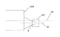
図3は、特に、導光板223の側端面に対するLED素子221の配置を示す概略断面図である。LED素子221は、導光板223の前面と底面との間の中間面A2に対して、LED素子221の発光面Bの中心軸A1が、導光板223の中間面A2よりも反射シート224に近い底面側にずらして配置されている。さらに、LED素子221の発光面Bの中心軸A1が中間面A2から導光板223の厚さの1/4以上ずれていることが好ましい。
さらに、具体的には、上記に加えて、図3に示すように、LED素子221は、導光板223の前面と底面との間の中間面A2に対して、LED素子221の発光面Bの導光板223の厚さ方向の両端部が、導光板223の底面側に含まれるように配置されていることがより好ましい。FIG. 3 is a schematic cross-sectional view showing the arrangement of the
Further, specifically, in addition to the above, as shown in FIG. 3, the
図4(a)は、導光板223の前面と底面との間の中間面A2に対して、LED素子221の発光面Bの中心軸A1を中間面A2に合わせた場合の導光板223内の光路を示す概略断面図である。図4(b)は、LED素子221の発光面Bの中心軸A1を中間面A2より底面側にずらした場合の導光板223内の光路を示す概略断面図である。図4(c)は、LED素子221の発光面Bの中心軸A1を中間面A2より前面側にずらした場合の光路を示す概略断面図である。 FIG. 4 (a) shows the inside of the
図4(a)に示すように、LED素子221の発光面Bの中心軸A1を中間面A2に合わせた場合には、底面の反射シート224を反射した反射光は端部から距離Lで前面側に出射する。一方、図4(b)に示すように、LED素子221の発光面の中心軸A1を底面側にずらした場合、底面の反射シート224を反射した反射光は端部から距離L1で前面側に出射する。上記のように、導光板223の厚さ方向で底面側にLED素子221を配置することによって、底面の反射シート224で反射して前面側から出射する距離をより短くできる。これによって、前面側で筐体101aによって液晶表示部210の端部を覆う距離を短くできる。なお、図4(c)に示すように、LED素子221の発光面の中心軸A1を前面側にずらした場合、底面の反射シート224を反射した反射光は端部から距離L2で前面側に出射する。 As shown in FIG. 4A, when the central axis A1 of the light emitting surface B of the
導光板223に入射した光は、導光板223を通過する間に前方散乱粒子226によって散乱されるが、導光板223への入射端部近傍では光が拡散しにくく直進する。したがって、図4(a)〜(c)に示すように、LED素子221からの出射角が同じ場合には、LED素子221から出射し、導光板223の側端面から入射した光が、底面の反射シート224を反射して導光板223の前面側から出射する距離L、L1、L2は、L1<L<L2となる。つまり、LED素子221の発光面Bの中心軸A1を導光板223の中間面A2よりも反射シート224に近い底面側にずらした方が、底面の反射シート224を反射して導光板223の前面側から出射する距離を短くできる。 The light incident on the
したがって、導光板223の端部において、液晶表示部210に均一に光を入射させるための導光板223の端部領域Hの長さを短くすることができ、画像表示装置100の額縁部を小さくし画像表示装置100を全体に小さくできる。 Therefore, the length of the end region H of the
また、この場合には、導光板223の厚みを薄くする必要もない。そのために、バックライト光源部の剛性を確保することができ、耐衝撃性、耐振動性を有する画像表示装置を実現できる。さらに、LED素子221として、より小さなLED素子を用いることができるため、画像表示装置100の導光板223の長辺方向に画像表示サイズ当たりに多数のLED素子を配列することができる。そのため、個々のLED素子への入力を低減して輝度を確保することができる。また、その場合には、ここのLED素子の入力の可変範囲を大きく取れ、屋内、屋外でも使用可能なように、輝度のダイナミックレンジを広くすることも可能となる。 In this case, it is not necessary to reduce the thickness of the
(実施の形態2)
図5は、本発明の実施の形態2に係る画像表示装置のバックライト光源部の構成を示す部分断面図である。実施の形態2に係る画像表示装置は、実施の形態1で述べた画像表示装置100と基本構成は同様であるが、実施の形態1とはLED素子の配列が異なっている。すなわち、本発明の実施の形態2では、図4に示すように、LED素子221は、導光板223の前面と底面との間の中間面A2に対して、LED素子221の発光面Bの導光板223の厚さ方向の両端部が、導光板223の前面側に含まれるように配置されている点で相違する。(Embodiment 2)
FIG. 5 is a partial cross-sectional view showing the configuration of the backlight light source unit of the image display apparatus according to Embodiment 2 of the present invention. The basic structure of the image display device according to the second embodiment is the same as that of the
実施の形態2に係る画像表示装置では、LED素子221を導光板223の前面側に設けているので、底面側の反射シート224で反射して前面に出射するまでの光路長が長くなる。このため、反射シート224で反射されたあと前面に出射するまでの光拡散効果が大きくなり、明領域と暗領域とが生じることによる、いわゆる明暗現象(蛍現象)を解消する効果が得られる。 In the image display device according to Embodiment 2, since the
(実施の形態3)
図6は、本発明の実施の形態3に係る画像表示装置のバックライト光源部の構成を示す部分断面図である。実施の形態3に係る画像表示装置は、実施の形態1で述べた画像表示装置100と基本構成は同様であるが、実施の形態1とはLED素子の配列が異なっている。すなわち、本発明の実施の形態3では、図6に示すように、導光板223の厚み方向に対してLED素子221として、上段LED素子221aと下段LED素子221bの2段配置としている。この場合、上段LED素子221aと下段LED素子221bの光照射の発光面Bの中心軸A1は、導光板223の厚み方向の中間面A2とずれている。さらに、具体的には、上段LED素子221aは、導光板223の前面と底面との間の中間面A2に対して、LED素子221aの発光面Bの導光板223の厚さ方向の両端部が、導光板223の前面側に含まれるように配置されている。下段LED素子221bは、導光板223の前面と底面との間の中間面A2に対して、LED素子221bの発光面Bの導光板223の厚さ方向の両端部が、導光板223の底面側に含まれるように配置されている。(Embodiment 3)
FIG. 6 is a partial cross-sectional view showing the configuration of the backlight light source unit of the image display apparatus according to Embodiment 3 of the present invention. The basic configuration of the image display device according to the third embodiment is the same as that of the
さらに、本発明の実施の形態3においては、図6に示すように、下段LED素子221bは、導光板223の背面に設置された反射シート224の基板227と同一面に設けた絶縁板228に接合されており、上段LED素子221aは絶縁板228aに接合されている。これらの絶縁板228a、228bは、コの字形状として開口部240を有する放熱板232の、開口部240側に熱伝導性の両面接着剤230a、230bを介して接合している。放熱板232は、熱伝導性の良好な材料、例えばアルミニウム、銅などの金属材料などによって形成され、コの字形状の垂直部232bには放熱フィン234が設けられている。 Furthermore, in Embodiment 3 of the present invention, as shown in FIG. 6, the
このように、本発明の実施の形態3では、導光板223の端面に対するLED素子221の配列を、導光板223の厚み方向に上下2段の配列としている。したがって、本発明の実施の形態3によれば、一つの導光板223に対して、従来に比べてLED素子を多数配列することができる。 As described above, in Embodiment 3 of the present invention, the
例えば、従来は10.4インチの表示サイズの液晶パネルに対して、短辺側にLED素子を36個配置し、画面輝度を最大で250cd/mm2程度としていた。しかし、本発明の実施の形態3によれば、LED素子221として、小さく、かつ出力効率の高いLED素子を用いて、上段LED素子221a、下段LED素子221bとしてそれぞれ60個配列することが可能となる。この場合、上段LED素子221a、あるいは下段LED素子221bだけで最大1000cd/mm2の輝度を実現できる。さらに、上段LED素子221aと下段LED素子221bとの同時使用によれば最大2000cd/mm2の輝度を実現できる。For example, conventionally, 36 LED elements are arranged on the short side with respect to a liquid crystal panel having a display size of 10.4 inches, and the screen brightness is about 250 cd / mm2 at the maximum. However, according to Embodiment 3 of the present invention, it is possible to arrange 60
したがって、本発明の実施の形態3によれば、個々のLED素子221a、221bへの入力を制御したり、上段LED素子221aと下段LED素子221bとをそれぞれ制御したり、あるいはこれらを組み合わせて制御することによって、極めて輝度のダイナミックレンジが広い画像表示装置を実現できる。そのため、これらの画像表示装置を搭載した情報処理装置を、屋内や屋外の明るさの環境に合わせて自由に使用できる。また、極めて汎用性が高くポータビリティ性を高めた情報処理装置を実現できる。 Therefore, according to Embodiment 3 of the present invention, the input to the
また、本発明の実施の形態3では、LED素子221からの発熱を放熱する放熱板として、コの字形状の放熱板232を用い、その開口部240に上段LED素子221a、下段LED素子221bを配置するようにしている。さらに、放熱板232の垂直部232bには外部との放熱面積を増加させる放熱フィン234を設けている。そのために、それぞれのLED素子から発生する熱を効果的に放熱させることができ放熱板232を一体で形成して、それぞれのLED素子の冷却効率を高めることができる。 In Embodiment 3 of the present invention, a U-shaped heat dissipation plate 232 is used as a heat dissipation plate that dissipates the heat generated from the
(実施の形態4)
図7(a)は、本発明の実施の形態4における画像表示装置のバックライト光源部のLED素子221の配列を示す概略平面図である。図7(a)では、上段LED素子221aと、上段LED素子221aから出射して導光板223に入射する入射光250を実線で示している。一方、下段LED素子221bと、下段LED素子221bから出射して導光板223に入射する入射光251を破線で示している。一方、図7(b)は、画像表示装置のバックライト光源部のLED素子を同一面内で一列に配置した構成を示す平面図である。図7(a)に示すように、実施の形態4に係る画像表示装置では、LED素子221は、導光板223の厚さ方向からみて、上段LED素子221aと、下段LED素子221bとを交互に配置している。また、導光板223の側端面から見ると、上段LED素子221aと下段LED素子221bとをジグザグ配置している。(Embodiment 4)
FIG. 7A is a schematic plan view showing an array of
実施の形態1で述べたように、導光板223に入射した光は、導光板223を通過する間に前方散乱粒子226によって散乱されるが、導光板223への入射端部近傍では光が拡散しにくく直進する。そのため、図7(b)に示すように、LED素子221を同一面内で一列のみで配列した場合には、導光板223への入射端部近傍で光度分布に明領域Eと暗領域Fとが発生する明暗現象(蛍現象)が発生する。すなわち、隣り合うLED素子221からの光が重畳される部分ではそれ以外の領域よりも明るくなる明領域Eが発生する。 As described in the first embodiment, the light incident on the
このような明暗現象は、導光板223の端部から所定距離だけ離れた領域では、導光板223内に分散配置された前方散乱粒子226によって光が拡散するため発生しなくなる。したがって、画像表示装置の有効表示領域に明暗現象が発生する領域が入らないように、画像表示装置100の額縁部長さを上記所定距離だけ長くする必要がある。この額縁部長さが長くなると、それだけ有効表示領域が狭くなってしまう。 Such a light and dark phenomenon does not occur in a region separated from the end of the
一方、図7(a)に示すように、本発明の実施の形態4では、導光板223の平面に対して、上段LED素子221aと下段LED素子221bとが交互になるように配置している。そのため、上段LED素子221aからの入射光250と、下段LED素子221bからの入射光251とがそれぞれ重畳されると共に、光拡散効果によって全ての領域で明るい状態となり、明暗現象(蛍現象)の発生を抑制することができる。 On the other hand, as shown in FIG. 7A, in the fourth embodiment of the present invention, the
したがって、光の重畳による明暗現象を解消して、均一な光度分布の画像表示装置を実現し、画像表示装置の額縁部長さも短くすることができる。 Therefore, the light and dark phenomenon due to the superimposition of light can be eliminated, an image display device with a uniform light intensity distribution can be realized, and the frame length of the image display device can be shortened.
本発明に係る画像表示装置は、輝度の調節が可能で、且つ、高輝度、長寿命、小型の画像表示装置を実現し、携帯型の情報処理装置用の画像表示装置として有用である。 The image display device according to the present invention is capable of adjusting the luminance, realizes a high-luminance, long-life, small-sized image display device, and is useful as an image display device for a portable information processing device.
100 画像表示装置
101 筐体
102 液晶パネル
103 前面ガラス基板
104 背面ガラス基板
210 液晶表示部
211 射出側偏光板
212 液晶本体部
213 入射側偏光板
220 バックライト光源部
221 LED素子
221a 上段LED素子
221b 下段LED素子
222 白色光
223 導光板
224 反射シート
225 プリズムシート
226 前方散乱粒子
227 基板
228,228a,228b 絶縁板
229,232 放熱板
230,230a,230b 両面接着剤
231,234 放熱フィン
232b 垂直部
240 開口部
250,251 入射光DESCRIPTION OF
Claims (8)
Translated fromJapanese前記液晶表示部の表示面と相対する裏面に面して設けられ、前面で前記液晶表示部の裏面に面すると共に、前記前面と対向する底面に反射シートを有し、前記前面及び前記底面と垂直な側端面から入射した光を前記底面の前記反射シートで反射して前記前面側に導く導光板と、
前記導光板の前記側端面に対向する発光面から前記側端面に対して光照射するLED素子と、
を備え、
前記LED素子は、前記導光板の前記前面と前記底面との間の中間面に対して、前記LED素子の発光面の中心軸が、前記導光板の前記底面側又は前記前面側のいずれかにずれて配置されている、画像表示装置。A liquid crystal display,
The liquid crystal display unit is provided so as to face the back surface facing the display surface, faces the back surface of the liquid crystal display unit on the front surface, and has a reflection sheet on the bottom surface facing the front surface, the front surface and the bottom surface, A light guide plate that reflects light incident from a vertical side end surface by the reflection sheet on the bottom surface and guides the light to the front surface side;
An LED element that emits light to the side end surface from a light emitting surface facing the side end surface of the light guide plate;
With
In the LED element, the central axis of the light emitting surface of the LED element is either on the bottom surface side or the front surface side of the light guide plate with respect to the intermediate surface between the front surface and the bottom surface of the light guide plate. An image display device that is displaced.
前記導光板の前記前面と前記底面との間の中間面に対して、前記LED素子の発光面の前記導光板の厚さ方向の両端部が、前記導光板の前記前面側に含まれるように配置された上段LED素子と、
前記導光板の前記前面と前記底面との間の中間面に対して、前記LED素子の発光面の前記導光板の厚さ方向の両端部が、前記導光板の前記底面側に含まれるように配置された下段LED素子と、
を有することを特徴とする請求項1に記載の画像表示装置。The LED element is
Both ends of the light emitting surface of the LED element in the thickness direction of the light guide plate are included on the front side of the light guide plate with respect to an intermediate surface between the front surface and the bottom surface of the light guide plate. An upper LED element disposed;
Both end portions of the light emitting surface of the LED element in the thickness direction of the light guide plate are included on the bottom surface side of the light guide plate with respect to an intermediate surface between the front surface and the bottom surface of the light guide plate. A lower LED element disposed;
The image display apparatus according to claim 1, further comprising:
前記上段LED素子と前記下段LED素子とは、前記放熱板の前記開口部に配置されていることを特徴とする請求項4又は5に記載の画像表示装置。Further comprising a heat sink having an opening that opens toward the side end face of the light guide plate,
The image display device according to claim 4, wherein the upper LED element and the lower LED element are disposed in the opening of the heat radiating plate.
Priority Applications (2)
| Application Number | Priority Date | Filing Date | Title |
|---|---|---|---|
| JP2009049343AJP2009244861A (en) | 2008-03-13 | 2009-03-03 | Image display apparatus |
| US12/402,831US20090231264A1 (en) | 2008-03-13 | 2009-03-12 | Image display aparatus |
Applications Claiming Priority (2)
| Application Number | Priority Date | Filing Date | Title |
|---|---|---|---|
| JP2008063665 | 2008-03-13 | ||
| JP2009049343AJP2009244861A (en) | 2008-03-13 | 2009-03-03 | Image display apparatus |
Publications (1)
| Publication Number | Publication Date |
|---|---|
| JP2009244861Atrue JP2009244861A (en) | 2009-10-22 |
Family
ID=41062487
Family Applications (1)
| Application Number | Title | Priority Date | Filing Date |
|---|---|---|---|
| JP2009049343APendingJP2009244861A (en) | 2008-03-13 | 2009-03-03 | Image display apparatus |
Country Status (2)
| Country | Link |
|---|---|
| US (1) | US20090231264A1 (en) |
| JP (1) | JP2009244861A (en) |
Cited By (3)
| Publication number | Priority date | Publication date | Assignee | Title |
|---|---|---|---|---|
| KR101211722B1 (en)* | 2010-03-16 | 2012-12-18 | 엘지이노텍 주식회사 | Back light umit within resin layer for light-guide and LCD using the same |
| KR101269952B1 (en)* | 2010-03-16 | 2013-05-31 | 엘지이노텍 주식회사 | Back light unit within resin layer for light-guide and LCD using the same |
| USRE48690E1 (en) | 2011-09-09 | 2021-08-17 | Lg Innotek Co., Ltd. | Light unit and a LCD liquid crystal display comprising the light unit |
Families Citing this family (5)
| Publication number | Priority date | Publication date | Assignee | Title |
|---|---|---|---|---|
| KR100964466B1 (en)* | 2009-11-24 | 2010-06-16 | 엘지전자 주식회사 | Display apparatus |
| KR100964467B1 (en)* | 2009-11-24 | 2010-06-16 | 엘지전자 주식회사 | Display apparatus |
| US9488772B2 (en)* | 2011-07-11 | 2016-11-08 | Seiko Epson Corporation | Display device, electronic apparatus and illumination device |
| JP2013175301A (en)* | 2012-02-23 | 2013-09-05 | Sharp Corp | Light source module and liquid crystal display device |
| US9939672B2 (en)* | 2014-06-13 | 2018-04-10 | Apple Inc. | Electronic device with heat spreading film |
Citations (8)
| Publication number | Priority date | Publication date | Assignee | Title |
|---|---|---|---|---|
| JPH08313902A (en)* | 1995-05-15 | 1996-11-29 | Rohm Co Ltd | Liquid crystal display device |
| JP2004342472A (en)* | 2003-05-16 | 2004-12-02 | Advanced Display Inc | Planar light source device and display device using the same |
| JP2005174820A (en)* | 2003-12-12 | 2005-06-30 | Advanced Display Inc | Planar light source device, and liquid crystal display device using the same |
| JP2005196989A (en)* | 2003-12-26 | 2005-07-21 | Fujitsu Display Technologies Corp | Backlight and liquid crystal display device |
| JP2006023654A (en)* | 2004-07-09 | 2006-01-26 | Kyocera Corp | Liquid crystal display |
| JP2007066605A (en)* | 2005-08-30 | 2007-03-15 | Optrex Corp | Planar lighting system |
| JP2007173233A (en)* | 2005-12-19 | 2007-07-05 | Avago Technologies Ecbu Ip (Singapore) Pte Ltd | Method and device consisting of providing heat sink, flexible printed circuit board fitted to at least part of the heat sink, and light source mounted on the flexible printed circuit board |
| JP2008027756A (en)* | 2006-07-21 | 2008-02-07 | Fujifilm Corp | Light guide plate, planar illumination device using the same, and liquid crystal display device |
Family Cites Families (7)
| Publication number | Priority date | Publication date | Assignee | Title |
|---|---|---|---|---|
| JP3368110B2 (en)* | 1995-08-01 | 2003-01-20 | キヤノン株式会社 | Light source device and optical equipment |
| JP4231607B2 (en)* | 1999-12-13 | 2009-03-04 | 日東電工株式会社 | Surface light source device and liquid crystal display device |
| AU2002359708A1 (en)* | 2001-12-14 | 2003-07-15 | Digital Optics International Corporation | Uniform illumination system |
| US7012655B2 (en)* | 2003-03-28 | 2006-03-14 | Lg.Philips Lcd Co., Ltd. | Liquid crystal display device with digitizer |
| US20060221610A1 (en)* | 2005-04-01 | 2006-10-05 | Chew Tong F | Light-emitting apparatus having a plurality of overlapping panels forming recesses from which light is emitted |
| US7513669B2 (en)* | 2005-08-01 | 2009-04-07 | Avago Technologies General Ip (Singapore) Pte. Ltd. | Light source for LCD back-lit displays |
| US7826703B2 (en)* | 2005-08-17 | 2010-11-02 | Fujifilm Corporation | Planar illuminating device |
- 2009
- 2009-03-03JPJP2009049343Apatent/JP2009244861A/enactivePending
- 2009-03-12USUS12/402,831patent/US20090231264A1/ennot_activeAbandoned
Patent Citations (8)
| Publication number | Priority date | Publication date | Assignee | Title |
|---|---|---|---|---|
| JPH08313902A (en)* | 1995-05-15 | 1996-11-29 | Rohm Co Ltd | Liquid crystal display device |
| JP2004342472A (en)* | 2003-05-16 | 2004-12-02 | Advanced Display Inc | Planar light source device and display device using the same |
| JP2005174820A (en)* | 2003-12-12 | 2005-06-30 | Advanced Display Inc | Planar light source device, and liquid crystal display device using the same |
| JP2005196989A (en)* | 2003-12-26 | 2005-07-21 | Fujitsu Display Technologies Corp | Backlight and liquid crystal display device |
| JP2006023654A (en)* | 2004-07-09 | 2006-01-26 | Kyocera Corp | Liquid crystal display |
| JP2007066605A (en)* | 2005-08-30 | 2007-03-15 | Optrex Corp | Planar lighting system |
| JP2007173233A (en)* | 2005-12-19 | 2007-07-05 | Avago Technologies Ecbu Ip (Singapore) Pte Ltd | Method and device consisting of providing heat sink, flexible printed circuit board fitted to at least part of the heat sink, and light source mounted on the flexible printed circuit board |
| JP2008027756A (en)* | 2006-07-21 | 2008-02-07 | Fujifilm Corp | Light guide plate, planar illumination device using the same, and liquid crystal display device |
Cited By (4)
| Publication number | Priority date | Publication date | Assignee | Title |
|---|---|---|---|---|
| KR101211722B1 (en)* | 2010-03-16 | 2012-12-18 | 엘지이노텍 주식회사 | Back light umit within resin layer for light-guide and LCD using the same |
| KR101269952B1 (en)* | 2010-03-16 | 2013-05-31 | 엘지이노텍 주식회사 | Back light unit within resin layer for light-guide and LCD using the same |
| USRE48690E1 (en) | 2011-09-09 | 2021-08-17 | Lg Innotek Co., Ltd. | Light unit and a LCD liquid crystal display comprising the light unit |
| USRE50289E1 (en) | 2011-09-09 | 2025-02-04 | Lg Innotek Co., Ltd. | Light unit and a LCD liquid crystal display comprising the light unit |
Also Published As
| Publication number | Publication date |
|---|---|
| US20090231264A1 (en) | 2009-09-17 |
Similar Documents
| Publication | Publication Date | Title |
|---|---|---|
| JP4590283B2 (en) | Backlight unit and liquid crystal display device including the same | |
| JP5026798B2 (en) | LED lighting device and liquid crystal display device using the same | |
| CN100523934C (en) | Heat dissipation device and display unit | |
| JP4968666B2 (en) | Backlight device and liquid crystal display device | |
| JP5064528B2 (en) | Backlight unit and liquid crystal display device including the same | |
| JP2009244861A (en) | Image display apparatus | |
| US20060164858A1 (en) | Backlight assembly and display apparatus having the same | |
| JP4701642B2 (en) | Display device | |
| CN104508359B (en) | Planar light source device and liquid crystal indicator | |
| JPWO2009093583A1 (en) | Display device and light emitting device | |
| JP2008304630A (en) | Liquid crystal display | |
| JPWO2008032460A1 (en) | Backlight device and display device using the same | |
| JP2006310221A (en) | Edge input type backlight and liquid crystal display device | |
| US20160291397A1 (en) | Display device | |
| JP2006059607A (en) | Heat radiation device and display device | |
| JP2004186004A (en) | Illumination device and liquid crystal display device having the same | |
| JP2010097908A (en) | Backlight unit and liquid crystal display device | |
| JP4777469B1 (en) | Illumination device and image display device including the same | |
| CN103133945A (en) | Backlight module for providing light source to display panel and display device thereof | |
| JP2010177076A (en) | Tandem surface light source device, and liquid crystal display device using the same | |
| WO2015012135A1 (en) | Lighting unit and liquid crystal display device | |
| JP5657727B2 (en) | Liquid crystal display device and television receiver | |
| JP2013218125A (en) | Liquid-crystal display | |
| JP2007250458A (en) | Edge input type backlight | |
| JP2006058486A (en) | Heatsink and display device |
Legal Events
| Date | Code | Title | Description |
|---|---|---|---|
| A621 | Written request for application examination | Free format text:JAPANESE INTERMEDIATE CODE: A621 Effective date:20120224 | |
| A977 | Report on retrieval | Free format text:JAPANESE INTERMEDIATE CODE: A971007 Effective date:20130111 | |
| A131 | Notification of reasons for refusal | Free format text:JAPANESE INTERMEDIATE CODE: A131 Effective date:20130122 | |
| A02 | Decision of refusal | Free format text:JAPANESE INTERMEDIATE CODE: A02 Effective date:20130521 |