JP2009238244A - Method and device for adjusting memory operation from variously arranged memory components - Google Patents
Method and device for adjusting memory operation from variously arranged memory componentsDownload PDFInfo
- Publication number
- JP2009238244A JP2009238244AJP2009162534AJP2009162534AJP2009238244AJP 2009238244 AJP2009238244 AJP 2009238244AJP 2009162534 AJP2009162534 AJP 2009162534AJP 2009162534 AJP2009162534 AJP 2009162534AJP 2009238244 AJP2009238244 AJP 2009238244A
- Authority
- JP
- Japan
- Prior art keywords
- memory
- slice
- component
- clock
- time interval
- Prior art date
- Legal status (The legal status is an assumption and is not a legal conclusion. Google has not performed a legal analysis and makes no representation as to the accuracy of the status listed.)
- Granted
Links
Images


Classifications
- G—PHYSICS
- G06—COMPUTING OR CALCULATING; COUNTING
- G06F—ELECTRIC DIGITAL DATA PROCESSING
- G06F13/00—Interconnection of, or transfer of information or other signals between, memories, input/output devices or central processing units
- G06F13/38—Information transfer, e.g. on bus
- G06F13/42—Bus transfer protocol, e.g. handshake; Synchronisation
- G06F13/4204—Bus transfer protocol, e.g. handshake; Synchronisation on a parallel bus
- G06F13/4234—Bus transfer protocol, e.g. handshake; Synchronisation on a parallel bus being a memory bus
- G06F13/4243—Bus transfer protocol, e.g. handshake; Synchronisation on a parallel bus being a memory bus with synchronous protocol
- G—PHYSICS
- G11—INFORMATION STORAGE
- G11C—STATIC STORES
- G11C11/00—Digital stores characterised by the use of particular electric or magnetic storage elements; Storage elements therefor
- G11C11/21—Digital stores characterised by the use of particular electric or magnetic storage elements; Storage elements therefor using electric elements
- G11C11/34—Digital stores characterised by the use of particular electric or magnetic storage elements; Storage elements therefor using electric elements using semiconductor devices
- G11C11/40—Digital stores characterised by the use of particular electric or magnetic storage elements; Storage elements therefor using electric elements using semiconductor devices using transistors
- G11C11/401—Digital stores characterised by the use of particular electric or magnetic storage elements; Storage elements therefor using electric elements using semiconductor devices using transistors forming cells needing refreshing or charge regeneration, i.e. dynamic cells
- G11C11/4063—Auxiliary circuits, e.g. for addressing, decoding, driving, writing, sensing or timing
- G11C11/407—Auxiliary circuits, e.g. for addressing, decoding, driving, writing, sensing or timing for memory cells of the field-effect type
- G11C11/4076—Timing circuits
- G—PHYSICS
- G06—COMPUTING OR CALCULATING; COUNTING
- G06F—ELECTRIC DIGITAL DATA PROCESSING
- G06F1/00—Details not covered by groups G06F3/00 - G06F13/00 and G06F21/00
- G06F1/04—Generating or distributing clock signals or signals derived directly therefrom
- G06F1/06—Clock generators producing several clock signals
- G—PHYSICS
- G06—COMPUTING OR CALCULATING; COUNTING
- G06F—ELECTRIC DIGITAL DATA PROCESSING
- G06F1/00—Details not covered by groups G06F3/00 - G06F13/00 and G06F21/00
- G06F1/04—Generating or distributing clock signals or signals derived directly therefrom
- G06F1/10—Distribution of clock signals, e.g. skew
- G06F1/105—Distribution of clock signals, e.g. skew in which the distribution is at least partially optical
- G—PHYSICS
- G06—COMPUTING OR CALCULATING; COUNTING
- G06F—ELECTRIC DIGITAL DATA PROCESSING
- G06F1/00—Details not covered by groups G06F3/00 - G06F13/00 and G06F21/00
- G06F1/04—Generating or distributing clock signals or signals derived directly therefrom
- G06F1/12—Synchronisation of different clock signals provided by a plurality of clock generators
- G—PHYSICS
- G06—COMPUTING OR CALCULATING; COUNTING
- G06F—ELECTRIC DIGITAL DATA PROCESSING
- G06F13/00—Interconnection of, or transfer of information or other signals between, memories, input/output devices or central processing units
- G06F13/14—Handling requests for interconnection or transfer
- G06F13/16—Handling requests for interconnection or transfer for access to memory bus
- G06F13/1668—Details of memory controller
- G06F13/1684—Details of memory controller using multiple buses
- G—PHYSICS
- G06—COMPUTING OR CALCULATING; COUNTING
- G06F—ELECTRIC DIGITAL DATA PROCESSING
- G06F13/00—Interconnection of, or transfer of information or other signals between, memories, input/output devices or central processing units
- G06F13/14—Handling requests for interconnection or transfer
- G06F13/16—Handling requests for interconnection or transfer for access to memory bus
- G06F13/1668—Details of memory controller
- G06F13/1689—Synchronisation and timing concerns
- G—PHYSICS
- G06—COMPUTING OR CALCULATING; COUNTING
- G06F—ELECTRIC DIGITAL DATA PROCESSING
- G06F13/00—Interconnection of, or transfer of information or other signals between, memories, input/output devices or central processing units
- G06F13/14—Handling requests for interconnection or transfer
- G06F13/16—Handling requests for interconnection or transfer for access to memory bus
- G06F13/1668—Details of memory controller
- G06F13/1694—Configuration of memory controller to different memory types
- G—PHYSICS
- G06—COMPUTING OR CALCULATING; COUNTING
- G06F—ELECTRIC DIGITAL DATA PROCESSING
- G06F13/00—Interconnection of, or transfer of information or other signals between, memories, input/output devices or central processing units
- G06F13/38—Information transfer, e.g. on bus
- G06F13/40—Bus structure
- G06F13/4063—Device-to-bus coupling
- G06F13/4068—Electrical coupling
- G06F13/4086—Bus impedance matching, e.g. termination
- G—PHYSICS
- G06—COMPUTING OR CALCULATING; COUNTING
- G06F—ELECTRIC DIGITAL DATA PROCESSING
- G06F3/00—Input arrangements for transferring data to be processed into a form capable of being handled by the computer; Output arrangements for transferring data from processing unit to output unit, e.g. interface arrangements
- G06F3/06—Digital input from, or digital output to, record carriers, e.g. RAID, emulated record carriers or networked record carriers
- G06F3/0601—Interfaces specially adapted for storage systems
- G06F3/0602—Interfaces specially adapted for storage systems specifically adapted to achieve a particular effect
- G06F3/0604—Improving or facilitating administration, e.g. storage management
- G—PHYSICS
- G06—COMPUTING OR CALCULATING; COUNTING
- G06F—ELECTRIC DIGITAL DATA PROCESSING
- G06F3/00—Input arrangements for transferring data to be processed into a form capable of being handled by the computer; Output arrangements for transferring data from processing unit to output unit, e.g. interface arrangements
- G06F3/06—Digital input from, or digital output to, record carriers, e.g. RAID, emulated record carriers or networked record carriers
- G06F3/0601—Interfaces specially adapted for storage systems
- G06F3/0628—Interfaces specially adapted for storage systems making use of a particular technique
- G06F3/0655—Vertical data movement, i.e. input-output transfer; data movement between one or more hosts and one or more storage devices
- G06F3/0658—Controller construction arrangements
- G—PHYSICS
- G06—COMPUTING OR CALCULATING; COUNTING
- G06F—ELECTRIC DIGITAL DATA PROCESSING
- G06F3/00—Input arrangements for transferring data to be processed into a form capable of being handled by the computer; Output arrangements for transferring data from processing unit to output unit, e.g. interface arrangements
- G06F3/06—Digital input from, or digital output to, record carriers, e.g. RAID, emulated record carriers or networked record carriers
- G06F3/0601—Interfaces specially adapted for storage systems
- G06F3/0668—Interfaces specially adapted for storage systems adopting a particular infrastructure
- G06F3/0671—In-line storage system
- G06F3/0673—Single storage device
- G—PHYSICS
- G11—INFORMATION STORAGE
- G11C—STATIC STORES
- G11C11/00—Digital stores characterised by the use of particular electric or magnetic storage elements; Storage elements therefor
- G11C11/21—Digital stores characterised by the use of particular electric or magnetic storage elements; Storage elements therefor using electric elements
- G11C11/34—Digital stores characterised by the use of particular electric or magnetic storage elements; Storage elements therefor using electric elements using semiconductor devices
- G11C11/40—Digital stores characterised by the use of particular electric or magnetic storage elements; Storage elements therefor using electric elements using semiconductor devices using transistors
- G11C11/401—Digital stores characterised by the use of particular electric or magnetic storage elements; Storage elements therefor using electric elements using semiconductor devices using transistors forming cells needing refreshing or charge regeneration, i.e. dynamic cells
- G11C11/4063—Auxiliary circuits, e.g. for addressing, decoding, driving, writing, sensing or timing
- G11C11/407—Auxiliary circuits, e.g. for addressing, decoding, driving, writing, sensing or timing for memory cells of the field-effect type
- G11C11/409—Read-write [R-W] circuits
- G11C11/4096—Input/output [I/O] data management or control circuits, e.g. reading or writing circuits, I/O drivers or bit-line switches
- G—PHYSICS
- G11—INFORMATION STORAGE
- G11C—STATIC STORES
- G11C29/00—Checking stores for correct operation ; Subsequent repair; Testing stores during standby or offline operation
- G11C29/02—Detection or location of defective auxiliary circuits, e.g. defective refresh counters
- G—PHYSICS
- G11—INFORMATION STORAGE
- G11C—STATIC STORES
- G11C29/00—Checking stores for correct operation ; Subsequent repair; Testing stores during standby or offline operation
- G11C29/02—Detection or location of defective auxiliary circuits, e.g. defective refresh counters
- G11C29/022—Detection or location of defective auxiliary circuits, e.g. defective refresh counters in I/O circuitry
- G—PHYSICS
- G11—INFORMATION STORAGE
- G11C—STATIC STORES
- G11C29/00—Checking stores for correct operation ; Subsequent repair; Testing stores during standby or offline operation
- G11C29/02—Detection or location of defective auxiliary circuits, e.g. defective refresh counters
- G11C29/023—Detection or location of defective auxiliary circuits, e.g. defective refresh counters in clock generator or timing circuitry
- G—PHYSICS
- G11—INFORMATION STORAGE
- G11C—STATIC STORES
- G11C29/00—Checking stores for correct operation ; Subsequent repair; Testing stores during standby or offline operation
- G11C29/02—Detection or location of defective auxiliary circuits, e.g. defective refresh counters
- G11C29/028—Detection or location of defective auxiliary circuits, e.g. defective refresh counters with adaption or trimming of parameters
- G—PHYSICS
- G11—INFORMATION STORAGE
- G11C—STATIC STORES
- G11C29/00—Checking stores for correct operation ; Subsequent repair; Testing stores during standby or offline operation
- G11C29/04—Detection or location of defective memory elements, e.g. cell constructio details, timing of test signals
- G11C29/50—Marginal testing, e.g. race, voltage or current testing
- G11C29/50008—Marginal testing, e.g. race, voltage or current testing of impedance
- G—PHYSICS
- G11—INFORMATION STORAGE
- G11C—STATIC STORES
- G11C29/00—Checking stores for correct operation ; Subsequent repair; Testing stores during standby or offline operation
- G11C29/04—Detection or location of defective memory elements, e.g. cell constructio details, timing of test signals
- G11C29/50—Marginal testing, e.g. race, voltage or current testing
- G11C29/50012—Marginal testing, e.g. race, voltage or current testing of timing
- G—PHYSICS
- G11—INFORMATION STORAGE
- G11C—STATIC STORES
- G11C5/00—Details of stores covered by group G11C11/00
- G11C5/06—Arrangements for interconnecting storage elements electrically, e.g. by wiring
- G11C5/063—Voltage and signal distribution in integrated semi-conductor memory access lines, e.g. word-line, bit-line, cross-over resistance, propagation delay
- G—PHYSICS
- G11—INFORMATION STORAGE
- G11C—STATIC STORES
- G11C7/00—Arrangements for writing information into, or reading information out from, a digital store
- G11C7/10—Input/output [I/O] data interface arrangements, e.g. I/O data control circuits, I/O data buffers
- G11C7/1051—Data output circuits, e.g. read-out amplifiers, data output buffers, data output registers, data output level conversion circuits
- G—PHYSICS
- G11—INFORMATION STORAGE
- G11C—STATIC STORES
- G11C7/00—Arrangements for writing information into, or reading information out from, a digital store
- G11C7/10—Input/output [I/O] data interface arrangements, e.g. I/O data control circuits, I/O data buffers
- G11C7/1072—Input/output [I/O] data interface arrangements, e.g. I/O data control circuits, I/O data buffers for memories with random access ports synchronised on clock signal pulse trains, e.g. synchronous memories, self timed memories
- G—PHYSICS
- G11—INFORMATION STORAGE
- G11C—STATIC STORES
- G11C7/00—Arrangements for writing information into, or reading information out from, a digital store
- G11C7/10—Input/output [I/O] data interface arrangements, e.g. I/O data control circuits, I/O data buffers
- G11C7/1078—Data input circuits, e.g. write amplifiers, data input buffers, data input registers, data input level conversion circuits
- G—PHYSICS
- G11—INFORMATION STORAGE
- G11C—STATIC STORES
- G11C7/00—Arrangements for writing information into, or reading information out from, a digital store
- G11C7/22—Read-write [R-W] timing or clocking circuits; Read-write [R-W] control signal generators or management
- G—PHYSICS
- G11—INFORMATION STORAGE
- G11C—STATIC STORES
- G11C7/00—Arrangements for writing information into, or reading information out from, a digital store
- G11C7/22—Read-write [R-W] timing or clocking circuits; Read-write [R-W] control signal generators or management
- G11C7/222—Clock generating, synchronizing or distributing circuits within memory device
- G—PHYSICS
- G11—INFORMATION STORAGE
- G11C—STATIC STORES
- G11C8/00—Arrangements for selecting an address in a digital store
- G11C8/18—Address timing or clocking circuits; Address control signal generation or management, e.g. for row address strobe [RAS] or column address strobe [CAS] signals
- G—PHYSICS
- G11—INFORMATION STORAGE
- G11C—STATIC STORES
- G11C7/00—Arrangements for writing information into, or reading information out from, a digital store
- G11C7/04—Arrangements for writing information into, or reading information out from, a digital store with means for avoiding disturbances due to temperature effects
Landscapes
- Engineering & Computer Science (AREA)
- Theoretical Computer Science (AREA)
- General Engineering & Computer Science (AREA)
- Physics & Mathematics (AREA)
- General Physics & Mathematics (AREA)
- Computer Hardware Design (AREA)
- Microelectronics & Electronic Packaging (AREA)
- Human Computer Interaction (AREA)
- Databases & Information Systems (AREA)
- Dram (AREA)
- Memory System (AREA)
- Measurement Of Velocity Or Position Using Acoustic Or Ultrasonic Waves (AREA)
- Static Random-Access Memory (AREA)
Abstract
Description
Translated fromJapanese本発明は、全般的には情報の蓄積および検索に関し、具体的には、メモリ・コンポーネントの調整に関する。 The present invention relates generally to information storage and retrieval, and in particular to the coordination of memory components.
コンピュータおよびデータ処理機器の能力が高まるにつれて、ユーザは、それらの機器に対するますます高まる要求を課す応用例を開発してきた。したがって、所与の時間の間により多くの情報を処理することに対する、継続的に高まる要求がある。所与の時間の間により多くの情報を処理する方法の1つが、情報の各要素をより短い時間で処理することである。時間が短縮されるにつれて、電子信号の通信を支配する物理的な速度の限界に近づく。遅延なしで情報の電子表現を移動できることが理想的であるが、そのような遅延は回避不能である。実際、遅延が回避不能であるばかりではなく、遅延の量が距離の関数なので、遅延は、通信する装置の相対的な位置に従って変動する。 As the capabilities of computers and data processing equipment have increased, users have developed applications that place increasing demands on those equipment. Thus, there is a continuously increasing demand for processing more information for a given time. One way to process more information during a given time is to process each element of information in a shorter time. As time is reduced, the physical speed limits governing electronic signal communication are approached. Ideally, the electronic representation of information can be moved without delay, but such delay is unavoidable. In fact, not only is the delay unavoidable, but since the amount of delay is a function of distance, the delay varies according to the relative position of the communicating devices.
単一の電子デバイスの能力に限界があるので、メモリ・コンポーネントなどのデバイスを多数組み合わせて、システムの総合性能を高めるために一緒に機能させることが望ましいことがしばしばである。しかし、デバイスは、空間内の同一の位置にすべてが同時に存在することができないので、ある面積にわたって異なる位置に配置されたデバイスを有するシステムの動作に対する考慮が必要である。 Because the capabilities of a single electronic device are limited, it is often desirable to combine multiple devices, such as memory components, to work together to increase the overall performance of the system. However, since devices cannot all exist at the same location in space, consideration must be given to the operation of a system having devices located at different locations over an area.
従来は、デバイスの動作のタイミングが、デバイスの位置の変動がその動作にとって問題になる点まで加速されていなかった。しかし、性能の要求が高まったので、従来のタイミング・パラダイムが、進歩に対する障害になった。 Conventionally, the timing of device operation has not been accelerated to the point where variations in the position of the device are problematic for the operation. However, as performance requirements have increased, the traditional timing paradigm has become an obstacle to progress.
既存のメモリ・システムの一例では、DDR(double data rate)メモリ・コンポーネントが使用される。このメモリ・システムには、メモリ・コントローラとメモリ・モジュールが含まれる。伝搬遅延が、メモリ・コントローラとメモリ・モジュールの間のアドレス・バスに沿って発生する。もう1つの伝搬遅延が、メモリ・コントローラとメモリ・モジュールの間のデータ・バスに沿って発生する。 An example of an existing memory system uses a DDR (double data rate) memory component. The memory system includes a memory controller and a memory module. Propagation delay occurs along the address bus between the memory controller and the memory module. Another propagation delay occurs along the data bus between the memory controller and the memory module.
メモリ・モジュール内の制御信号および制御クロック信号の分配が、厳密な制約を受ける。通常、制御線は、各メモリ・コンポーネントへの長さが等しくなるようにルーティングされる。「スター」トポロジまたは「2進木」トポロジが、通常は使用され、この場合に、スターの各スポークまたは2進木の各枝が、同一の長さを有する。その意図は、メモリ・モジュールの異なるメモリ・コンポーネントの間の制御信号および制御クロック信号のタイミングの変動を除去することであるが、各メモリ・コンポーネントへのワイヤの長さの平衡化は、システム性能を損なう(一部のパスが、必要以上に長くなる)。さらに、等しい長さをもたらすようにワイヤをルーティングする必要によって、メモリ・コンポーネントの数が制限され、メモリ・コンポーネントの接続が複雑になる。 The distribution of control signals and control clock signals within the memory module is subject to strict constraints. Typically, control lines are routed so that the length to each memory component is equal. A “star” or “binary tree” topology is typically used, where each spoke of the star or each branch of the binary tree has the same length. The intent is to eliminate timing variations in the control and control clock signals between the different memory components of the memory module, but balancing the lengths of the wires to each memory component (Some paths are longer than necessary). In addition, the need to route wires to provide equal lengths limits the number of memory components and complicates memory component connections.
そのようなDDRシステムでは、データ・ストローブ信号が、データ読取動作とデータ書込動作の両方のタイミングを制御するのに使用される。データ・ストローブ信号は、周期的なタイミング信号ではなく、データが転送される時に限ってアサートされる。制御信号のタイミング信号は、周期的なクロックである。書込データのデータ・ストローブ信号は、制御信号のクロックに整列される。読取データのストローブは、アドレス・バスに沿った伝搬遅延とデータ・バスに沿った伝搬遅延の合計に等しい、制御クロックに対する相対的な遅延だけ遅延される。読取転送の後に書込転送が続く時には、シグナリングの一時停止を設けて、使用されるさまざまな信号線に沿った干渉を防がなければならない。そのような一時停止は、システム性能を低下させる。 In such DDR systems, the data strobe signal is used to control the timing of both data read and data write operations. The data strobe signal is asserted only when data is transferred, not a periodic timing signal. The timing signal of the control signal is a periodic clock. The data strobe signal of the write data is aligned with the control signal clock. The read data strobe is delayed by a delay relative to the control clock equal to the sum of the propagation delay along the address bus and the propagation delay along the data bus. When a read transfer is followed by a write transfer, a signaling pause must be provided to prevent interference along the various signal lines used. Such a pause reduces system performance.
そのようなシステムは、複数の形で制約を受ける。第1に、制御ワイヤが、スター・トポロジまたは2進木ルーティングを有するので、スタブ(スポークまたは枝の終点)で反射が発生する。反射は、信号の整定時間を増やし、制御ワイヤの転送帯域幅を制限する。その結果、制御ワイヤ上で1つの情報が駆動されるタイム・インターバルが、信号波面が制御ワイヤの一端から他端まで伝搬するのに要する時間より長くなる。さらに、より多くのモジュールがシステムに追加される時に、より多くのワイヤ・スタブが、データ・バスの各導体に追加され、これによって、スタブからの反射が増える。これによって、信号の整定時間が増加し、データ・バスの転送帯域幅がさらに制限される。 Such systems are constrained in several ways. First, because the control wire has a star topology or binary tree routing, reflection occurs at the stub (spoke or branch endpoint). Reflection increases the settling time of the signal and limits the transfer bandwidth of the control wire. As a result, the time interval at which one piece of information is driven on the control wire is longer than the time required for the signal wavefront to propagate from one end of the control wire to the other. Furthermore, as more modules are added to the system, more wire stubs are added to each conductor of the data bus, thereby increasing reflection from the stubs. This increases the signal settling time and further limits the data bus transfer bandwidth.
また、このシステム内のアドレス・バスに沿った伝搬遅延とデータ・バスに沿った伝搬遅延の間の関係に対する制約があるので、メモリ・コンポーネントのタイミング・パラメータに違反せずに動作周波数を高めることは困難である。クロック信号が、別のクロック信号と独立である場合に、これらのクロック信号およびそれに関係するコンポーネントは、異なるクロック・ドメインであるとみなされる。メモリ・コンポーネント内で、書込データ・レシーバは、メモリ・コンポーネントのロジックの残りと異なるクロック・ドメインで動作しており、ドメイン・クロッシング回路は、これらの2つのドメインの間の限られた量のスキューだけに対処する。データのシグナリング・レートを高めると、このスキュー・パラメータ(時間単位で測定された時の)が減り、基板上のデータ・ワイヤと制御ワイヤの間のルーティング不一致がタイミング違反を引き起こす機会が増える。 There are also constraints on the relationship between the propagation delay along the address bus and the data bus in this system to increase the operating frequency without violating the memory component timing parameters. It is difficult. If a clock signal is independent of another clock signal, these clock signals and their associated components are considered to be in different clock domains. Within the memory component, the write data receiver is operating in a different clock domain than the rest of the logic of the memory component, and the domain crossing circuit is a limited amount between these two domains. Deal with skew only. Increasing the data signaling rate reduces this skew parameter (when measured in hours) and increases the chance that routing mismatch between the data and control wires on the board will cause timing violations.
また、ほとんどのDDRシステムは、アドレス・バスおよびデータ・バスの伝搬遅延の長さ(時間単位)に対する厳密な制限を有する。これは、通常、コントローラの読取データ・レシーバ・クロック・ドメインからコントローラの残りの部分が使用するクロック・ドメインへのクロッシングのために含まれるロジックと、メモリ・コントローラとによって課せられる制限である。通常は、これらの伝搬遅延の合計の長さに対する制限(クロック・サイクル単位で表される)もある。マザーボード・レイアウトのためにこの合計が大きくなりすぎる(時間単位で測定された時に)場合に、システムの信号レートを下げなければならない場合があるが、これによって性能が低下する。 Most DDR systems also have strict limits on the length of the propagation delay (in time units) of the address and data buses. This is usually a limitation imposed by the memory controller and the logic involved for crossing from the controller read data receiver clock domain to the clock domain used by the rest of the controller. There is also usually a limit (expressed in clock cycles) to the total length of these propagation delays. If this sum is too large due to the motherboard layout (when measured in hours), the signal rate of the system may have to be reduced, which reduces performance.
既存のメモリ・システムのもう1つの例では、制御ワイヤおよびデータ・バスが、メモリ・コントローラに接続され、各メモリ・モジュール上のメモリ・コンポーネントを通って一緒にルーティングされる。1つのクロックが、書込データ信号と制御信号のタイミングを制御するのに使用され、もう1つのクロックが、読取データのタイミングを制御するのに使用される。これらの2つのクロックは、メモリ・コントローラで整列される。前の従来技術の例と異なって、これらの2つのタイミング信号は、別々のワイヤで搬送される。 In another example of an existing memory system, control wires and data buses are connected to the memory controller and routed together through the memory components on each memory module. One clock is used to control the timing of the write data signal and the control signal, and the other clock is used to control the timing of the read data. These two clocks are aligned with the memory controller. Unlike the previous prior art example, these two timing signals are carried on separate wires.
そのような代替システムでは、複数の組の制御ワイヤと1つのデータ・バスを使用して、メモリ・コントローラを1つまたは複数のメモリ・コンポーネントに相互結合することができる。別の組の制御ワイヤが必要なので、追加のコストと複雑さが導入されるが、これは、望ましくない。また、大容量メモリ・システムが必要な場合に、各データ・バス上のメモリ・コンポーネントの数が、相対的に多くなる。これは、データ・バス上の最大信号レートを制限する傾向を有し、これによって性能が制限される。 In such an alternative system, multiple sets of control wires and a single data bus may be used to interconnect the memory controller to one or more memory components. The need for another set of control wires introduces additional cost and complexity, which is undesirable. Also, when a large capacity memory system is required, the number of memory components on each data bus is relatively large. This tends to limit the maximum signal rate on the data bus, which limits performance.
既存のメモリ・システムのもう1つの例が、ハンセン(Hansen)他に1998年7月7日に発行された米国特許第5778419号に見られる。ハンセン他の特許は、パケットおよびアービトレーションを使用する高帯域幅インターフェースを有するダイナミック・ランダム・アクセス・メモリ(DRAM)に関するが、そのようなDRAMは、その有用性を制限するいくつかの不利益をこうむる。 Another example of an existing memory system can be found in US Pat. No. 5,778,419 issued July 7, 1998 to Hansen et al. Although Hansen et al. Relates to dynamic random access memory (DRAM) with a high bandwidth interface that uses packets and arbitration, such DRAM suffers from several disadvantages that limit its usefulness. .
したがって、さまざまな位置に配置されたメモリ・コンポーネントの間でメモリ動作を調整する技法が必要である。 Therefore, there is a need for techniques for coordinating memory operations between memory components located at various locations.
本発明は、メモリ・コントローラ・コンポーネントと、スライスを含むメモリ・コンポーネントのランクと、該メモリ・コントローラ・コンポーネントをメモリ・コンポーネントの該ランクに結合し、該メモリ・コントローラ・コンポーネントをメモリ・コンポーネントの該ランクの該スライスに結合する導体であって、導体のうちで、アドレス信号、書込データ信号、および読取データ信号からなる群から選択された信号を搬送する1つの伝搬遅延が、該信号によって表される情報の要素が該導体に印加される時間の量より長く、該導体が、該メモリ・コントローラ・コンポーネントを該ランクの該スライスのそれぞれに連続して接続する共通アドレス・バスと、該メモリ・コントローラ・コンポーネントを該ランクの該スライスのそれぞれに接続する別のデータ・バスとを含むことを特徴とするメモリ・システムである。 The present invention relates to a memory controller component, a rank of the memory component that includes the slice, the memory controller component coupled to the rank of the memory component, and the memory controller component to the rank of the memory component. A conductor coupled to the slice of rank, wherein one propagation delay carrying a signal selected from the group consisting of an address signal, a write data signal, and a read data signal is represented by the signal. A common address bus that continuously connects the memory controller component to each of the slices of the rank, the memory element being longer than the amount of time applied to the conductor; A controller component for each slice of the rank A memory system which comprises a separate data bus connecting to.
さまざまな位置に配置されたメモリ・コンポーネントの間でメモリ動作を調整する方法および装置を説明する。本発明の実施形態によれば、ウェーブ・パイプライン化が、複数のメモリ・コンポーネントに結合されたアドレス・バスに対して実施される。複数のメモリ・コンポーネントは、アドレス・バス伝搬遅延およびデータ・バス伝搬遅延に関する調整に従って構成される。アドレス信号および/または制御信号に関連する、これらの信号の伝搬遅延を複製するタイミング信号を使用して、メモリ動作を調整する。アドレス・バス伝搬遅延または共通アドレス・バス伝搬遅延は、メモリ・コントローラ・コンポーネントとメモリ・コンポーネントの間でアドレス・バスに沿って進む信号の遅延を指す。データ・バス伝搬遅延は、メモリ・コントローラ・コンポーネントとメモリ・コンポーネントの間でデータ・バスに沿って進む信号の遅延を指す。 A method and apparatus for coordinating memory operations between memory components located at various locations is described. According to embodiments of the present invention, wave pipelining is performed on an address bus coupled to a plurality of memory components. The plurality of memory components are configured in accordance with adjustments for address bus propagation delay and data bus propagation delay. A timing signal that replicates the propagation delay of these signals associated with address and / or control signals is used to coordinate memory operations. Address bus propagation delay or common address bus propagation delay refers to the delay of the signal traveling along the address bus between the memory controller component and the memory component. Data bus propagation delay refers to the delay of the signal traveling along the data bus between the memory controller component and the memory component.
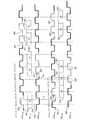
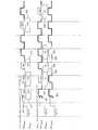
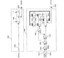
本発明の一実施形態によれば、メモリ・システムに、メモリ・コンポーネントの複数のランクおよび複数のスライスを提供する複数のメモリ・モジュールが含まれる。そのようなシステムは、図27に関して理解することができる。図27のメモリ・システムには、メモリ・モジュール2703およびメモリ・モジュール2730が含まれる。メモリ・モジュール2703には、メモリ・コンポーネント2716から2618を含むランクと、メモリ・コンポーネント2744から2746を含むもう1つのランクが含まれる。 According to one embodiment of the present invention, a memory system includes a plurality of memory modules that provide a plurality of ranks and a plurality of slices of memory components. Such a system can be understood with respect to FIG. The memory system of FIG. 27 includes a
このメモリ・システムは、メモリ・コントローラ・コンポーネントおよびメモリ・モジュールにまたがるスライスに編成される。図27のメモリ・システムには、メモリ・コントローラ2702の一部と、メモリ・コンポーネント2716および2744を含むメモリ・モジュール2703の一部と、メモリ・コンポーネント2731および2734を含むメモリ・モジュール2730の一部とを含むスライス2713が含まれる。図27のメモリ・システムには、メモリ・コントローラ2702のもう1つの部分と、メモリ・コンポーネント2717およびメモリ・コンポーネント2745を含むメモリ・モジュール2703のもう1つの部分と、メモリ・コンポーネント2732および2735を含むメモリ・モジュール2730のもう1つの部分とを含むもう1つのスライス2714が含まれる。図27のメモリ・システムには、さらに、メモリ・コントローラ2702のもう1つの部分と、メモリ・コンポーネント2718および2746を含むメモリ・モジュール2703のもう1つの部分と、メモリ・コンポーネント2733および2736を含むメモリ・モジュール2730のもう1つの部分とを含むもう1つのスライス2715が含まれる。 The memory system is organized into slices that span memory controller components and memory modules. The memory system of FIG. 27 includes a portion of
複数のモジュールを使用して実施することができる複数のスライスおよびランクを使用することによって、データ・バスまたはアドレス・バスがそれへの多数の接続を有する時に発生する可能性がある性能低下を回避すると同時に、メモリ・コントローラおよび複数のメモリ・コンポーネントの効率的な相互接続が可能になる。スライスごとに別々のデータ・バスを設けると、各データ・バスへの接続の数を、適度な数にすることができる。別々のデータ・バスは、互いに独立に異なる信号を搬送することができる。スライスに、1モジュールごとに1つまたは複数のメモリ・コンポーネントを含めることができる。たとえば、1つのスライスに、各ランクの1つのメモリ・コンポーネントを含めることができる。用語スライスが、スライスのうちでメモリ・コントローラを除く部分を指すのに使用される場合があることに留意されたい。この形で、メモリ・コントローラを、スライスに結合されているものとみなすことができる。複数のモジュールを使用することによって、メモリ・コンポーネントを、メモリ・コントローラへのパス長に従って編成できる。そのようなパス長のわずかな相違であっても、メモリ・コンポーネントのランクへの編成に従って管理することができる。ランクおよびモジュールに従ってメモリ・コンポーネントを編成することによって、アドレス信号および制御信号を、たとえばランクまたはモジュール内のアドレス・バスの共有を介して、効率的に分配できる。 By using multiple slices and ranks that can be implemented using multiple modules, avoid performance degradation that can occur when the data or address bus has multiple connections to it At the same time, an efficient interconnection of the memory controller and multiple memory components is possible. Providing a separate data bus for each slice allows the number of connections to each data bus to be moderate. Separate data buses can carry different signals independently of each other. A slice can include one or more memory components per module. For example, one slice can contain one memory component of each rank. Note that the term slice may be used to refer to the portion of the slice excluding the memory controller. In this manner, the memory controller can be considered as coupled to a slice. By using multiple modules, memory components can be organized according to the path length to the memory controller. Even such slight differences in path length can be managed according to the organization of memory components into ranks. By organizing memory components according to rank and module, address and control signals can be efficiently distributed, for example, through sharing of address buses within the rank or module.
一実施形態では、スライスに、データ・バスに結合された複数の要素が含まれると理解することができる。一例として、これらの要素には、メモリ・コントローラ・コンポーネントの一部、1モジュール上の1つまたは複数のメモリ・コンポーネント、および、任意選択として、別のモジュール上の1つまたは複数のメモリ・コンポーネントを含めることができる。一実施形態では、ランクに、共通アドレス・バスによって結合された複数のメモリ・コンポーネントが含まれると理解することができる。共通アドレス・バスを、任意選択として、1つまたは複数のモジュール上の複数のランクに結合することができる。共通アドレス・バスは、メモリ・コントローラ・コンポーネントを、1ランク内のスライスのそれぞれに連続して接続することができ、これによって、共通アドレス・バスを、ランクの第1スライスからランクの第2スライスへ、およびランクの第2スライスからランクの第3スライスへとルーティングすることが可能になる。そのような構成によって、共通アドレス・バスのルーティングを単純にすることができる。 In one embodiment, it can be understood that a slice includes a plurality of elements coupled to a data bus. By way of example, these elements include part of a memory controller component, one or more memory components on a module, and optionally one or more memory components on another module Can be included. In one embodiment, it can be understood that a rank includes a plurality of memory components coupled by a common address bus. A common address bus can optionally be coupled to multiple ranks on one or more modules. The common address bus can connect memory controller components in succession to each of the slices in a rank so that the common address bus is routed from the first slice of the rank to the second slice of the rank. And from the second slice of the rank to the third slice of the rank. Such a configuration can simplify common address bus routing.
説明のために、ある概念を例示するために、単純化された形のメモリ・システムをまず説明し、その後で、複数のモジュールおよびランクを含むより複雑なメモリ・システムを、本明細書で説明する。 For purposes of explanation, a simplified form of a memory system will first be described to illustrate certain concepts, followed by a more complex memory system including multiple modules and ranks described herein. To do.
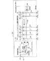
図1は、本発明の実施形態を実施することができる、メモリ・コンポーネントの単一のランクを有するメモリ・システムを示すブロック図である。メモリ・システム101には、メモリ・コントローラ・コンポーネント102およびメモリ・モジュール103が含まれる。アドレス・バス107に沿って伝搬するアドレス信号および制御信号に関連するタイミング信号として働くアドレス・クロック信号がアドレス・クロック104によって供給される。アドレス・クロック104は、アドレス・クロック導体109に沿ってそのアドレス・クロック信号を供給する。アドレス・クロック導体109は、メモリ・コントローラ・コンポーネント102およびメモリ・モジュール103に結合される。アドレス信号および制御信号を、時々、単にアドレス信号またはアドレス・バスと称する。しかし、制御信号は、アドレス信号と共通のトポロジに従ってルーティングすることができるので、これらの単語は、使用される時に、アドレス信号または制御信号もしくはその両方を含むものとして理解されなければならない。 FIG. 1 is a block diagram illustrating a memory system having a single rank of memory components in which embodiments of the present invention may be implemented. The
書込クロック105は、書込動作中にデータ・バス108に沿って伝搬するデータ信号に関連するタイミング信号として働く書込クロック信号を供給する。書込クロック105は、書込クロック導体110に沿ってその書込クロック信号を供給し、書込クロック導体110は、メモリ・コントローラ・コンポーネント102およびメモリ・モジュール103に結合される。読取クロック106は、読取動作中にデータ・バス108に沿って伝搬するデータ信号に関連するタイミング信号として働く読取クロック信号を供給する。読取クロック106は、読取クロック導体111に沿ってその読取クロック信号を供給し、読取クロック導体111は、メモリ・コントローラ・コンポーネント102およびメモリ・モジュール103に結合される。 Write
終端コンポーネント120が、メモリ・コントローラ・コンポーネント102の近くでデータ・バス108に結合される。一例として、終端コンポーネント120を、メモリ・コントローラ・コンポーネント102に組み込むことができる。終端コンポーネント121が、メモリ・モジュール103の近くでデータ・バス108に結合される。終端コンポーネント121は、メモリ・モジュール103に組み込まれることが好ましい。終端コンポーネント123が、メモリ・モジュール103のメモリ・コンポーネント116の近くで書込クロック導体110に結合される。終端コンポーネント123は、メモリ・モジュール103に組み込まれることが好ましい。終端コンポーネント124が、メモリ・コントローラ・コンポーネント102の近くで読取クロック導体111に結合される。一例として、終端コンポーネント124を、メモリ・コントローラ・コンポーネント102に組み込むことができる。終端コンポーネント125が、メモリ・モジュール103のメモリ・コンポーネント116の近くで読取クロック導体111に結合される。終端コンポーネント125は、メモリ・モジュール103に組み込まれることが好ましい。終端コンポーネントでは、能動デバイス(たとえばトランジスタまたは他の半導体デバイス)または受動デバイス(たとえば抵抗、コンデンサ、インダクタ)を使用することができる。終端コンポーネントに、オープン接続を使用することができる。終端コンポーネントを、1つまたは複数のメモリ・コントローラ・コンポーネントもしくは1つまたは複数のメモリ・コンポーネントに組み込むことができ、また、モジュール上またはメイン回路基板上の別のコンポーネントとすることができる。 A
メモリ・モジュール103には、メモリ・コンポーネント116、117、および118のランク112が含まれる。メモリ・モジュール103は、各メモリ・コンポーネントが1つのスライスに対応するように編成される。メモリ・コンポーネント116は、スライス113に対応し、メモリ・コンポーネント117は、スライス114に対応し、メモリ・コンポーネント118は、スライス115に対応する。図1には示されていないが、スライス113に関して図示されている、データ・バスと、書込クロックおよび関連する導体と、読取クロックおよび関連する導体とに関連する特定の回路が、他のスライス114および115のそれぞれについて複製される。したがって、そのような回路は、図を簡単にするために図1に図示されていないが、そのようなスライス単位の専用の回路が、図示のメモリ・システムに含まれることが好ましいことを理解されたい。
メモリ・モジュール103内で、アドレス・バス107が、メモリ・コンポーネント116、117、および118のそれぞれに結合される。アドレス・クロック導体109が、メモリ・コンポーネント116、117、および118のそれぞれに結合される。メモリ・モジュール103内のアドレス・バス107の末端で、終端コンポーネント119が、アドレス・バス107に結合される。アドレス・クロック導体109の末端で、終端コンポーネント122が、アドレス・クロック導体109に結合される。 Within
図1のメモリ・システムでは、各データ信号導体が、1つのコントローラ・データ・バス・ノードを1つのメモリ・デバイス・データ・バス・ノードに接続する。しかし、制御信号導体およびアドレス信号導体のそれぞれが、1つのコントローラ・アドレス/制御バス・ノードを、メモリ・ランクの各メモリ・コンポーネント上のアドレス/制御バス・ノードに接続することが可能である。これは、複数の理由から可能になる。第1に、制御信号導体およびアドレス信号導体には、単一方向信号が流れる(信号波面が、コントローラからメモリ・デバイスに伝搬する)。両方向信号導体(データ信号導体など)上よりも、単一方向信号導体上の方が、よい信号完全性を維持するのが簡単である。第2に、アドレス信号と制御信号に、すべてのメモリ・デバイスについて同一の情報が含まれる。データ信号は、すべてのメモリ・デバイスについて異なる。各メモリ・デバイスについて異なる、いくつかの制御信号(書き込みイネーブル信号など)がある可能性があることに留意されたい。これらの信号は、単一方向データ信号として扱われ、この説明においてはデータ・バスの一部とみなされる。たとえば、いくつかの場合に、データ・バスに、多数のビットに対応するデータ信号線が含まれる場合があるが、いくつかの応用例で、データ・バスによって搬送されるビットの一部だけが、特定のメモリ動作についてメモリに書き込まれる場合がある。たとえば、16ビット・データ・バスに2バイトのデータが含まれるが、特定のメモリ動作中に、2バイトのうちの1バイトだけが、特定のメモリ・デバイスに書き込まれる場合がある。そのような例では、追加の制御信号を、データ信号がたどるものに類似するパスに沿って設けることができ、データ・ビット線上のデータを書き込むか否かを制御する制御信号が、データの遅延に全般的に一致する遅延を伴うパスに沿ってシステムをトラバースし、データの書込を制御する際の制御信号の使用が適当なタイミングを与えられるようにする。第3に、アドレス信号および制御信号のすべてのメモリ・デバイスへのルーティングによって、コントローラおよびメモリ・モジュールのインターフェースのピンが節約される。 In the memory system of FIG. 1, each data signal conductor connects one controller data bus node to one memory device data bus node. However, each control signal conductor and address signal conductor can connect one controller address / control bus node to an address / control bus node on each memory component of the memory rank. This is possible for several reasons. First, the control signal conductor and the address signal conductor carry a unidirectional signal (a signal wavefront propagates from the controller to the memory device). It is easier to maintain good signal integrity on a unidirectional signal conductor than on a bidirectional signal conductor (such as a data signal conductor). Second, the address signal and the control signal contain the same information for all memory devices. The data signal is different for all memory devices. Note that there may be several control signals (such as write enable signals) that are different for each memory device. These signals are treated as unidirectional data signals and are considered part of the data bus in this description. For example, in some cases, the data bus may include data signal lines corresponding to multiple bits, but in some applications, only a portion of the bits carried by the data bus , Certain memory operations may be written to memory. For example, a 16-bit data bus contains 2 bytes of data, but only one of the 2 bytes may be written to a particular memory device during a particular memory operation. In such an example, an additional control signal can be provided along a path similar to that followed by the data signal, and the control signal that controls whether or not to write data on the data bit line is a data delay. The system is traversed along a path with a delay that generally matches, so that the use of control signals in controlling the writing of data is given the proper timing. Third, routing of address and control signals to all memory devices saves controller and memory module interface pins.
その結果、制御信号およびアドレス信号が、データ信号の伝搬に使用されるワイヤより長いワイヤで伝搬されるようになる。これによって、いくつかの場合に、データ信号で、制御信号およびアドレス信号より高いシグナリング・レートを使用することが可能になる。 As a result, the control signal and the address signal are propagated over a wire longer than that used for propagation of the data signal. This in some cases allows the data signal to use a higher signaling rate than the control and address signals.
メモリ・システムの性能を損なわないようにするために、アドレス信号および制御信号を、本発明の実施形態に従って、ウェーブ・パイプライン化することができる。メモリ・システムは、ウェーブ・パイプライン化の助けになる複数の条件を満たすように構成される。第1に、複数のメモリ・コンポーネントが、ランクとして編成される。第2に、アドレス信号および制御信号の一部またはすべてが、ランクのすべてのメモリ・コンポーネントに共通する。第3に、共通のアドレス信号および制御信号が、低ひずみで(たとえばインピーダンスを制御されて)伝搬する。第4に、共通のアドレス信号および制御信号が、低シンボル間干渉で(たとえば単一終端または二重終端)伝搬する。 In order not to compromise the performance of the memory system, the address and control signals can be wave pipelined in accordance with embodiments of the present invention. The memory system is configured to satisfy a plurality of conditions that aid in wave pipelining. First, a plurality of memory components are organized as ranks. Second, some or all of the address and control signals are common to all memory components in the rank. Third, common address and control signals propagate with low distortion (eg, controlled impedance). Fourth, common address signals and control signals propagate with low intersymbol interference (eg, single termination or double termination).
ウェーブ・パイプライン化は、Tbit<Twireの時に発生し、ここで、タイミング・パラメータTwireは、コントローラで作られる波面が、信号を搬送するワイヤの端の終端コンポーネントに伝搬する時間遅延として定義され、タイミング・パラメータTbitは、ワイヤ上の連続する情報(ビット)の間のタイム・インターバルとして定義される。そのような情報は、個々のビットまたは、同時伝送用にエンコードされた複数のビットを表すことができる。ワイヤ上のウェーブ・パイプライン化された信号は、ワイヤに接続されたレシーバによってサンプリングされる入射波である。これは、一般に、波面が伝送線(たとえばワイヤ)の端から反射される前にサンプリングが行われることを意味する。 Wave pipelining occurs when Tbit <Twire, where the timing parameter Twire is defined as the time delay that the wavefront created by the controller propagates to the terminating component at the end of the wire carrying the signal, The timing parameter Tbit is defined as the time interval between successive information (bits) on the wire. Such information can represent individual bits or multiple bits encoded for simultaneous transmission. A wave pipelined signal on a wire is an incident wave sampled by a receiver connected to the wire. This generally means that the sampling takes place before the wavefront is reflected from the end of the transmission line (eg wire).
本発明の適用可能性を、複数の形でメモリ・コンポーネントの単一のランクから複数のランクに拡張することが可能である。第1に、メモリ・コンポーネントの複数のランクを、1つのメモリ・モジュールに実装することができる。第2に、複数のメモリ・モジュールを、1つのメモリ・システム内に実装することができる。第3に、データ信号導体を、各モジュールの専用、共有、または「チェインされる」ものとすることができる。チェイン化には、バスが1つのモジュールを通過できるようにすることと、そのモジュール上の適当な回路に接続することが含まれるが、その特定のモジュールから出た時に、別のモジュールに入るか終端に達することができるようにすることが含まれる。導体のそのようなチェイン化の例を、図29、32、および35と下に示し、さらに詳細に説明する。第4に、共通の制御信号導体およびアドレス信号導体を、各モジュールの専用、共有、またはチェインされるものとすることができる。第5に、データ信号導体を、各モジュール上で終端される伝送線または終端されるスタブとすることができる。この議論について、伝送線は、その伝送線を介する正しい信号伝送を保証するために反射および他の伝送線特性を考慮しなければならない、十分な長さを有する信号線を表すものと理解される。対照的に、終端されるスタブは、そのようなスタブに関連する寄生反射および他の伝送線特性を一般に無視することができる限られた長さを有すると理解される。第6に、共通の制御信号導体およびアドレス信号導体を、各モジュール上で終端される伝送線または終端されるスタブとすることができる。共有されるアドレス信号および制御信号をウェーブ・パイプライン化できるようにすることによって、それらのシグナリング・レートを高めることができ、これによってメモリ・システムの性能が向上する。 The applicability of the present invention can be extended in multiple ways from a single rank of memory components to multiple ranks. First, multiple ranks of memory components can be implemented in a single memory module. Second, multiple memory modules can be implemented in a single memory system. Third, data signal conductors can be dedicated, shared, or “chained” to each module. Chaining involves allowing a bus to pass through one module and connecting to the appropriate circuitry on that module, but when it leaves that particular module, can it enter another module? Includes allowing the end to be reached. Examples of such chaining of conductors are shown in FIGS. 29, 32 and 35 below and are described in further detail. Fourth, a common control signal conductor and address signal conductor can be dedicated, shared, or chained to each module. Fifth, the data signal conductor can be a transmission line terminated on each module or a terminated stub. For this discussion, a transmission line is understood to represent a signal line having a sufficient length that must take into account reflections and other transmission line characteristics to ensure correct signal transmission through the transmission line. . In contrast, terminated stubs are understood to have a limited length that can generally ignore the parasitic reflections and other transmission line characteristics associated with such stubs. Sixth, the common control and address signal conductors can be transmission lines terminated on each module or terminated stubs. By allowing the shared address and control signals to be wave pipelined, their signaling rate can be increased, thereby improving the performance of the memory system.
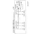
図2は、本発明の実施形態による、図1に示されたものなどのメモリ・システムのメモリ・コンポーネントのランクの1スライスのクロッキングの詳細を示すブロック図である。メモリ・コントローラ・コンポーネント102に、アドレス送出ブロック201が含まれ、アドレス送出ブロック201は、アドレス・バス107およびアドレス・クロック導体109に結合される。メモリ・コントローラ・コンポーネント102には、スライスごとに、データ送出ブロック202およびデータ受取ブロック203が含まれ、これらはデータ・バス108に結合される。データ送出ブロック202は、書込クロック導体110に結合され、データ受取ブロック203は、読取クロック導体111に結合される。 FIG. 2 is a block diagram illustrating details of one-slice clocking of ranks of memory components of a memory system, such as that shown in FIG. 1, in accordance with an embodiment of the present invention. The
メモリ・コンポーネント116などの各メモリ・コンポーネント内に、アドレス受取ブロック204、データ受取ブロック205、およびデータ送出ブロック206が設けられる。アドレス受取ブロック204は、アドレス・バス107およびアドレス・クロック導体109に結合される。データ受取ブロック205は、データ・バス108および書込クロック導体110に結合される。データ送出ブロック206は、データ・バス108および読取クロック導体111に結合される。 Within each memory component, such as
tPD0と表される伝搬遅延207が、アドレス・バス107に沿って、メモリ・コントローラ・コンポーネント102とメモリ・モジュール103の間に存在する。tPD1と表される伝搬遅延208が、アドレス・バス107に沿って、メモリ・モジュール103内に存在する。A
図2に表された基本トポロジは、複数の属性を有する。このトポロジには、メモリ・コントローラが含まれる。このトポロジには、単一のメモリ・モジュールが含まれる。このトポロジには、メモリ・コンポーネントの単一のランクが含まれる。このトポロジには、スライスされたデータ・バス(DQ)が含まれ、ワイヤの各スライスが、コントローラをメモリ・コンポーネントに接続する。このトポロジには、コントローラをすべてのメモリ・コンポーネントに接続する共通のアドレスおよび制御バス(Addr/CtrlまたはAC)が含まれる。ソース同期式クロック信号が、データ信号、制御信号、およびアドレス信号と共に流れる。制御信号およびアドレス信号は、単一方向であり、コントローラからメモリ・コンポーネントへ流れる。データ信号は、両方向であり、コントローラからメモリ・コンポーネントへ流れることができ(書込動作)、メモリ・コンポーネントからコントローラへ流れることができる(読取動作)。データ信号と同一のトポロジを有する制御信号がいくつかある場合があるが、それらの制御信号は、コントローラからメモリ・コンポーネントへ流れるのみである。そのような信号は、たとえば書込動作で書込データをマスクするのに使用することができる。これらは、この議論においては単一方向データ信号として扱うことができる。データ・ワイヤ、アドレス・ワイヤ、制御ワイヤ、およびクロック・ワイヤは、低ひずみで(たとえばインピーダンスを制御された導体に沿って)伝搬する。データ・ワイヤ、アドレス・ワイヤ、制御ワイヤ、およびクロック・ワイヤは、低シンボル間干渉で(たとえば単一方向信号の単一終端および両方向信号の二重終端がある)伝搬する。これらの属性は、明瞭さを保つためにリストされたものである。本発明が、これらの属性を用いて実践されることに制限されず、他のシステム・トポロジを含むように実践することができることを理解されたい。 The basic topology shown in FIG. 2 has a plurality of attributes. This topology includes a memory controller. This topology includes a single memory module. This topology includes a single rank of memory components. This topology includes a sliced data bus (DQ), where each slice of wire connects the controller to a memory component. This topology includes a common address and control bus (Addr / Ctrl or AC) that connects the controller to all memory components. A source synchronous clock signal flows with the data signal, the control signal, and the address signal. Control and address signals are unidirectional and flow from the controller to the memory component. Data signals are bidirectional and can flow from the controller to the memory component (write operation) and from the memory component to the controller (read operation). There may be several control signals that have the same topology as the data signals, but they only flow from the controller to the memory component. Such a signal can be used, for example, to mask write data in a write operation. These can be treated as unidirectional data signals in this discussion. Data wires, address wires, control wires, and clock wires propagate with low distortion (eg, along a conductor whose impedance is controlled). Data wires, address wires, control wires, and clock wires propagate with low intersymbol interference (eg, there is a single termination for unidirectional signals and a double termination for bidirectional signals). These attributes are listed for clarity. It should be understood that the present invention is not limited to being practiced with these attributes, but can be practiced to include other system topologies.
図2には、データ・バスおよびメモリ・コンポーネントのスライス番号(S={0、1、…、NS})およびモジュール番号(M={0、1})、に基づく2次元座標系がある。ここで、スライス番号「0」およびモジュール番号「0」が、コントローラを参照する。この座標系を用いると、ワイヤ上の異なる位置で信号に命名することができる。この座標系を用いると、複数のメモリ・ランクまたはメモリ・モジュールを有するトポロジへの拡張も可能になる。In FIG. 2 there is a two-dimensional coordinate system based on the data bus and memory component slice numbers (S = {0, 1,..., NS }) and module numbers (M = {0, 1}). . Here, the slice number “0” and the module number “0” refer to the controller. Using this coordinate system, signals can be named at different locations on the wire. Using this coordinate system also allows expansion to topologies with multiple memory ranks or memory modules.
図2には、3つのクロック・ソース(AClk信号を生成するアドレス・クロック104、WClk信号を生成する書込クロック105、およびRClk信号を生成する読取クロック106)も示されており、これらが、3種類の情報転送のためのクロッキング基準信号を生成する。これらのクロック・ソースのそれぞれが、それに関連する信号バスと並列のクロック・ワイヤを駆動する。システム内のクロック・ソースの位置は、クロック・ソースが対応するクロック信号を駆動する、クロック線上の物理的位置が、バス線の関係する駆動点に隣接し、特定のバスのクロックの伝搬が、一般に、関連するバス上の関係する情報の伝搬を追跡するようになっていることが好ましい。たとえば、アドレス・クロック(AClkクロック104)の位置決めは、アドレス信号がアドレス・バス107へ駆動される物理位置に近いことが好ましい。そのような構成では、アドレス・クロックが、回路全体を通じて伝搬する時に、アドレス・クロック信号線と全般的に同一のルートをたどるバスに沿って伝搬するアドレス信号が経験する遅延に類似する遅延を経験する。 Also shown in FIG. 2 are three clock sources: an
各バスのクロック信号は、関連するバスの信号の最大ビット・レートに関係する。この関係は、通常は、整数または整数比である。たとえば、最大データ・レートを、データ・クロック信号の周波数の2倍とすることができる。クロック・ソースの1つまたは2つを「仮想」クロック・ソースとすることも可能であり、この場合に、3つのクロック・ソースが、互いに整数分数比(N/M)関係になり、それらのいずれをも、フェーズ・ロック・ループ(PLL)技法を使用して周波数および位相をセットすることによって、他の2つのいずれかから合成することができる。仮想クロック・ソースは、回路内の実際のクロック・ソースの数を最小にすることができる手段を表す。たとえば、WClkクロックを、メモリ・デバイスが受け取るアドレス・クロック(AClk)から導出し、メモリ・デバイスが、外部ソースから実際にWClkクロックを受け取る必要をなくすことができる。したがって、メモリ・デバイスは、実際には独自の個別に生成されたWClkクロックを受け取らないが、AClkクロックから生成されたWClkクロックは、機能的に同等である。合成されたクロック信号の位相は、図示の位置のクロック・ソースによって生成された場合と同一になるように調整される。 Each bus clock signal is related to the maximum bit rate of the associated bus signal. This relationship is usually an integer or integer ratio. For example, the maximum data rate can be twice the frequency of the data clock signal. It is also possible for one or two of the clock sources to be “virtual” clock sources, in which case the three clock sources are in an integer fractional ratio (N / M) relationship to each other and their Either can be synthesized from either of the other two by setting the frequency and phase using a phase lock loop (PLL) technique. A virtual clock source represents a means by which the number of actual clock sources in the circuit can be minimized. For example, the WClk clock may be derived from an address clock (AClk) received by the memory device, eliminating the need for the memory device to actually receive the WClk clock from an external source. Thus, the memory device does not actually receive its own individually generated WClk clock, but the WClk clock generated from the AClk clock is functionally equivalent. The phase of the synthesized clock signal is adjusted to be the same as that generated by the clock source at the position shown.
図示のクロック信号のいずれでも、代替案では、情報が関連するバス上に存在する時に限ってアサートされる非周期的信号(たとえばストローブ制御信号)とすることができる。クロック・ソースに関して上で説明したように、非周期的信号ソースは、物理的な意味で、非周期的信号に関連する伝搬遅延がそれが対応するバス上の信号の伝搬遅延と全般的に一致するように、それが対応する適当なバスに隣接して位置決めされることが好ましい。 Any of the clock signals shown may alternatively be an aperiodic signal (eg, a strobe control signal) that is only asserted when information is present on the associated bus. As explained above with respect to clock sources, an aperiodic signal source is a physical meaning that the propagation delay associated with an aperiodic signal generally matches the propagation delay of the signal on which it corresponds. As such, it is preferably positioned adjacent to the corresponding appropriate bus.
図3は、他の図のタイミング図で使用されるアドレス・タイミングおよび制御タイミングの表記を示すタイミング図である。図3では、AClk信号301の立ち上がりエッジ302が、アドレス情報ACa 305の送出中の時刻307に発生する。AClk信号の立ち上がりエッジ303が、アドレス情報ACb306の送出中の時刻308に発生する。時刻308は、AClk信号301の次の立ち上がりエッジ304の時刻309より時間tCCだけ前に発生する。時間tCCは、メモリ・コントローラ・コンポーネントのクロック回路のサイクル・タイムを表す。タイミング図の破線は、信号のうちで、時間的にアドレス情報またはデータ情報と同時の部分を示すのに使用される。たとえば、AClk信号301には、アドレス情報ACa 305の存在に対応する時間的部分と、アドレス情報ACb 306の存在に対応するもう1つの時間的部分が含まれる。アドレス情報は、アドレス信号としてアドレス・バスを介して送出することができる。FIG. 3 is a timing diagram illustrating the notation of address timing and control timing used in the timing diagrams of the other figures. In FIG. 3, the rising edge 302 of the
1ビット/ワイヤがtCCごとに発生する場合には、アドレス・ビット311が、サイクル310中に送出される。2ビット/ワイヤがtCCごとに発生する場合には、アドレス・ビット313および314が、サイクル312中に送出される。4ビット/ワイヤがtCCごとに発生する場合には、アドレス・ビット316、317、318、および319が、サイクル315中に送出される。8ビット/ワイヤがtCCごとに発生する場合には、アドレス・ビット321、322、323、324、325、326、327、および328が、サイクル320中に送出される。各ビット・ウィンドウの駆動点およびサンプル点を、使用されるドライバおよびサンプラの回路技法に応じて、オフセット(1ビット時間すなわちtCC/NACまで)だけ遅らせるか進めることができることに留意されたい。パラメータNACおよびNDQは、それぞれアドレス/制御ワイヤおよびデータ・ワイヤのtCCごとのビット数を表す。一実施形態では、固定オフセットを使用する。駆動/サンプル点とビット・ウィンドウの間のオフセットは、駆動コンポーネントとサンプリング・コンポーネントの間で一貫性を有しなければならない。特定のシステムで、バスの駆動ポイントに関連するオフセットのいずれもが、システム全体を通じて一貫性を有することが好ましい。同様に、バスに関して理解されるサンプリング・オフセットも、一貫性を有しなければならない。たとえば、データが、あるデータ・バス線の関係するクロック信号の立ち上がりエッジに全般的に対応する点で駆動されることが期待される場合に、その理解されるオフセット(またはその不在)が、すべてのデータ線について一貫した形で使用されることが好ましい。バスへのデータの駆動に関連するオフセットを、そのバスによって搬送されるデータのサンプリングに関連するオフセットと完全に異なるものにすることができることに留意されたい。したがって、上の例を継続すると、全般的に立ち上がりエッジと同時に駆動されるデータのサンプル点は、立ち上がりエッジに対して180°位相はずれとし、データの有効ウィンドウがサンプリング点によってよりよくターゲティングされるようにすることができる。If one bit / wire occurs every tCC ,
図4は、他の図のタイミング図で使用されるデータ・タイミングの表記を示すタイミング図である。図4では、WClk信号401の立ち上がりエッジ402が、書込データ情報Da 405の送出中の時刻407に発生する。WClk信号401の立ち上がりエッジ403が、時刻408に発生する。WClk信号401の立ち上がりエッジ404が、読取データ情報Qb 406の送出中の時刻409に発生する。時刻407は、時刻408から時間tCCだけ離れており、時刻408は、時刻409から時間tCCだけ離れている。時間tCCは、クロック・サイクルの持続時間を表す。RClk信号410に、立ち上がりエッジ411および立ち上がりエッジ412が含まれる。これらの立ち上がりエッジを、RClk信号410のクロック・サイクルに対する基準として使用することができる。たとえば、書込データ情報Da 405の送出は、RClk信号410の、立ち上がりエッジ411を含むクロック・サイクル中に発生し、読取データ情報Qb406の送出は、RClk信号410の、立ち上がりエッジ412を含むクロック・サイクル中に発生する。当業者に明白であるように、アドレス・クロックに関連するクロック・サイクル・タイムは、読取クロックまたは書込クロックに関連するクロック・サイクル・タイムと異なるものとすることができる。FIG. 4 is a timing diagram illustrating the notation of data timing used in the timing diagrams of other diagrams. In FIG. 4, the rising
書込データ情報は、書き込まれる情報の要素であり、データ・バス上で書込データ信号として送出することができる。読取データ情報は、読み取られる情報の要素であり、データ・バス上で読取データ信号として送出することができる。表記Dxは、書込データ情報xを表すのに使用され、表記Qyは、読取データ情報yを表すのに使用される。信号は、アドレス信号、書込データ信号、読取データ信号、または他の信号のいずれであっても、要素タイム・インターバルと称する時間の間、導体またはバスに印加することができる。そのような要素タイム・インターバルを、タイミング信号を搬送する導体またはバス上で発生するイベントと関連付けることができ、そのようなイベントを、タイミング信号イベントと称する場合がある。そのようなタイミング信号の例には、クロック信号、別の信号または情報の要素から導出されるタイミング信号、および、タイミングをそこから導出することができる他の信号が含まれる。メモリ・アクセス動作では、アドレス信号がアドレス・バスに印加され始める時からそのアドレス信号に対応するデータ信号がデータ・バスに印加され始める時までの時間を、アクセス・タイム・インターバルと称することができる。 Write data information is an element of information to be written and can be sent out as a write data signal on the data bus. Read data information is an element of information to be read and can be sent as a read data signal on the data bus. The notation Dx is used to represent write data information x, and the notation Qy is used to represent read data information y. The signal, whether an address signal, a write data signal, a read data signal, or other signal, can be applied to a conductor or bus for a time period referred to as an element time interval. Such element time intervals can be associated with events that occur on conductors or buses that carry timing signals, and such events are sometimes referred to as timing signal events. Examples of such timing signals include a clock signal, a timing signal derived from another signal or element of information, and other signals from which timing can be derived. In a memory access operation, the time from when an address signal starts to be applied to the address bus to when the data signal corresponding to the address signal starts to be applied to the data bus can be referred to as an access time interval. .
1ビット/ワイヤがtCCごとに発生する場合には、データ・ビット415が、サイクル414中に送出される。2ビット/ワイヤがtCCごとに発生する場合には、データ・ビット417および418が、サイクル416中に送出される。4ビット/ワイヤがtCCごとに発生する場合には、データ・ビット420、421、422、および423が、サイクル419中に送出される。8ビット/ワイヤがtCCごとに発生する場合には、データ・ビット425、426、427、428、429、430、431、および432が、サイクル424中に送出される。各ビット・ウィンドウの駆動点およびサンプル点を、使用されるドライバおよびサンプラの回路技法に応じて、オフセット(1ビット時間すなわちtCC/NDQまで)だけ遅らせるか進めることができることに留意されたい。一実施形態では、固定オフセットを使用する。駆動/サンプル点とビット・ウィンドウの間のオフセットは、駆動コンポーネントとサンプリング・コンポーネントの間で一貫性を有しなければならない。たとえば、データがコントローラ側の適当なクロック信号の立ち上がりエッジにサンプリングされるように、データ・ウィンドウが位置決めされると仮定すると、有効なデータも回路内のその位置での対応するクロックの立ち上がりエッジに存在すると仮定されるように、類似する規約をメモリ・デバイスで使用しなければならない。If 1 bit / wire occurs every tCC , data bit 415 is sent out during
1ビット/ワイヤがtCCごとに発生する場合には、データ・ビット434が、サイクル433中に送出される。2ビット/ワイヤがtCCごとに発生する場合には、データ・ビット436および437が、サイクル435中に送出される。4ビット/ワイヤがtCCごとに発生する場合には、データ・ビット439、440、441、および442が、サイクル438中に送出される。8ビット/ワイヤがtCCごとに発生する場合には、データ・ビット444、445、446、447、448、449、450、および451が、サイクル443中に送出される。各ビット・ウィンドウの駆動点およびサンプル点を、使用されるドライバおよびサンプラの回路技法に応じて、オフセット(1ビット時間すなわちtCC/NDQまで)だけ遅らせるか進めることができることに留意されたい。一実施形態では、固定オフセットを使用する。駆動/サンプル点とビット・ウィンドウの間のオフセットは、駆動コンポーネントとサンプリング・コンポーネントの間で一貫性を有しなければならない。上で述べたように、特定のシステムで、あるバスの駆動点またはサンプリング点に関連するオフセットは、システム全体を通じて一貫性を有することが好ましい。If one bit / wire occurs every tCC , data bit 434 is sent during
メモリ・コンポーネントのカラム・サイクル・タイムは、連続するカラム・アクセス動作(読取または書込)を実行するのに必要なタイム・インターバルを表す。図示の例では、AClkクロック信号、RClkクロック信号、およびWClkクロック信号が、カラム・サイクル・タイムに等しいサイクル・タイムを有するものとして図示されている。当業者に明白であるように、システムで使用されるクロック信号のサイクル・タイムは、他の実施形態では、カラム・サイクル・タイムと異なるものとすることができる。 The memory component column cycle time represents the time interval required to perform successive column access operations (read or write). In the illustrated example, the AClk clock signal, the RClk clock signal, and the WClk clock signal are illustrated as having a cycle time equal to the column cycle time. As will be apparent to those skilled in the art, the cycle time of the clock signal used in the system may be different from the column cycle time in other embodiments.
その代わりに、クロックのすべてが、カラム・サイクル・タイムと異なるサイクル・タイムを有することができる。バス上での信号の送出または受取に適当な速度のクロックは、分配されるクロックと合成されたクロックの間に整数比または整数分数比がある限り、必ず、分配されるクロックから合成することができる。前に述べたように、必要なクロックのいずれであっても、他のバスからの分配されるクロックのいずれかから合成することができる。 Instead, all of the clocks can have a cycle time that is different from the column cycle time. A clock with the appropriate speed for sending or receiving signals on the bus must be synthesized from the distributed clock as long as there is an integer ratio or an integer fraction ratio between the distributed clock and the synthesized clock. it can. As previously mentioned, any required clock can be synthesized from any of the distributed clocks from other buses.
この説明では、タイミング図をできる限り単純にするために、各tCCインターバル中に各ワイヤ上で単一のビットがサンプリングされるか駆動されると仮定する。しかし、各tCCインターバル中に各信号ワイヤ上で送出されるビット数を、変更することができる。パラメータNACおよびNDQは、それぞれアドレス/制御ワイヤおよびデータ・ワイヤの、tCCごとのビット数を表す。分配されるクロックまたは合成されるクロックは、tCCごとに複数のビットを駆動し、サンプリングするのに適当なクロック・エッジを作るために逓倍される。各ビット・ウィンドウの駆動点およびサンプル点を、使用されるドライバおよびサンプラの回路技法に応じて、オフセット(1ビット時間すなわちtCC/NACまたはtCC/NDQまで)だけ遅らせるか進めることができることに留意されたい。一実施形態では、固定オフセットを使用する。駆動/サンプル点とビット・ウィンドウの間のオフセットは、駆動コンポーネントとサンプリング・コンポーネントの間で一貫性を有しなければならない。やはり、上で述べたように、特定のシステムで、あるバスの駆動点またはサンプリング点に関連するオフセットは、システム全体を通じて一貫性を有することが好ましい。In this description, it is assumed that a single bit is sampled or driven on each wire during each tCC interval to make the timing diagram as simple as possible. However, the number of bits sent on each signal wire during each tCC interval can be changed. The parameters NAC and NDQ represent the number of bits per tCC of the address / control wire and data wire, respectively. The distributed clock or synthesized clock is multiplied to create a clock edge suitable for driving and sampling multiple bits every tCC . Depending on the driver and sampler circuit technique used, each bit window drive point and sample point may be delayed or advanced by an offset (up to 1 bit time, ie, tCC / NAC or tCC / NDQ ) Note that you can. In one embodiment, a fixed offset is used. The offset between the drive / sample points and the bit window must be consistent between the drive component and the sampling component. Again, as noted above, in a particular system, the offset associated with a given bus drive or sampling point is preferably consistent throughout the system.
図5は、本発明の実施形態による、アドレスおよび制御バス(Addr/CtrlまたはACS、M)上で通信される信号のタイミングを示すタイミング図である。このバスには、このバスと本質的に同一のワイヤ・パスを見るクロック信号AClkS、Mが付随する。添字(S、M)は、特定のモジュールMまたは特定のスライスSでのバスまたはクロック信号を示す。コントローラは、スライス0になるように定義される。FIG. 5 is a timing diagram illustrating the timing of signals communicated on the address and control bus (Addr / Ctrl or ACS ,M ) according to an embodiment of the present invention. Associated with this bus is a clock signal AClkS ,M which looks at essentially the same wire path as this bus. The subscripts (S, M) indicate a bus or clock signal in a specific module M or a specific slice S. The controller is defined to be
AClkクロック信号501の波形に、メモリ・コントローラ・コンポーネントでのAClkクロック信号のタイミングが示されている。AClkクロック信号501の立ち上がりエッジ502が、時刻510に発生し、アドレス情報ACa 518の送出に関連する。AClkクロック信号501の立ち上がりエッジ503が、時刻511に発生し、アドレス情報ACb 519の送出に関連する。 The waveform of the
AClkクロック信号520の波形に、スライス1に配置されたメモリ・コンポーネントでのAClkクロック信号のタイミングが示されている。AClkクロック信号520は、信号501からtPD0の遅延だけ遅れている。たとえば、信号520の立ち上がりエッジ523は、信号501のエッジ502からtPD0の遅延だけ遅れている。アドレス情報ACa 537が、信号520の立ち上がりエッジ523に関連する。アドレス情報ACb 538が、信号520の立ち上がりエッジ525に関連する。The waveform of the
AClkクロック信号539の波形に、スライスNSに配置されたメモリ・コンポーネントでのAClkクロック信号のタイミングが示されている。AClkクロック信号539は、信号520からtPD1の遅延だけ遅れている。たとえば、信号539の立ち上がりエッジ541は、信号520のエッジ523からtPD1の遅延だけ遅れている。アドレス情報ACa 548が、信号539の立ち上がりエッジ541に関連する。アドレス情報ACb 549が、信号539の立ち上がりエッジ542に関連する。The waveform of
クロック信号AClkは、カラム・サイクル・タイムに対応するサイクル・タイムを有するものとして図示されている。前に述べたように、この信号は、コントローラおよびメモリ・コンポーネントがバス上の情報をサンプリングし、駆動するのに必要なタイミング点を生成できるように周波数および位相が制約される限り、より短いサイクル・タイムを有することもできる。同様に、バスは、tCCインターバルごとに送出される単一ビット/ワイヤを有するものとして図示されている。前に述べたように、コントローラおよびメモリ・コンポーネントが、バス上の情報をサンプリングし、駆動するのに必要なタイミング点を生成できるので、各tCCインターバルに複数のビットを転送することができる。バスの実際の駆動点(データ信号、アドレス信号、または制御信号もしくはこれらの組合せがバスに印加される点)が、示されたものからのオフセット(クロックの立ち上がりエッジおよび立ち下がりエッジに対して)を有することができ、これが、コントローラおよびメモリ・コンポーネント内の送出回路および受取回路の設計に依存することに留意されたい。一実施形態では、固定オフセットを使用する。駆動/サンプル点とビット・ウィンドウの間のオフセットは、駆動コンポーネントとサンプリング・コンポーネントの間で一貫性を有しなければならない。上で繰り返したように、特定のシステムで、あるバスの駆動点またはサンプリング点に関連するオフセットは、システム全体を通じて一貫性を有することが好ましい。Clock signal AClk is illustrated as having a cycle time corresponding to the column cycle time. As previously mentioned, this signal is a shorter cycle as long as the frequency and phase are constrained so that the controller and memory components can generate the timing points necessary to sample and drive the information on the bus.・ You can also have time. Similarly, the bus is illustrated as having a single bit / wire delivered every tCC interval. As previously mentioned, the controller and memory components can generate the timing points necessary to sample and drive the information on the bus so that multiple bits can be transferred in each tCC interval. The actual driving point of the bus (the point at which data signals, address signals, or control signals or combinations thereof are applied to the bus) are offset from what is shown (relative to the rising and falling edges of the clock) Note that this depends on the design of the sending and receiving circuits in the controller and memory components. In one embodiment, a fixed offset is used. The offset between the drive / sample points and the bit window must be consistent between the drive component and the sampling component. As repeated above, in a particular system, the offset associated with a given bus drive or sampling point is preferably consistent throughout the system.
図5で、クロックAClkS、MおよびバスACS、Mが、コントローラから第1スライスに伝搬する際に、tPD0の遅延があることに留意されたい。図示されているように、AClk信号520は、時間および空間においてAClk信号501からシフトされている。また、クロックAClkS、MおよびバスACS、Mが、第1スライスから最後のスライスNSに伝搬する際に、第2の遅延tPD1があることに留意されたい。クロックおよびバスが、各スライスの間を進む際に、tPD1/(NS−1)の遅延がある。この計算では、スライスの間の全般的に等しい間隔が仮定され、そのような物理的特性がシステムに存在しない場合には、遅延がこの式に従わないことに留意されたい。したがって、図示されているように、AClk信号539は、時間および空間においてAClk信号520からシフトされている。その結果、NS個のメモリ・コンポーネントのそれぞれが、時間的にわずかに異なる点で、アドレスおよび制御バスをサンプリングする。Note in FIG. 5 that there is a delay of tPD0 as the clocks AClkS ,M and buses ACS ,M propagate from the controller to the first slice. As shown,
図6は、本発明の実施形態による、データ・バス(DQS、M)上で通信される信号のタイミングを示すタイミング図である。このバスには、本質的にこのバスと同一のワイヤ・パスを見る2つのクロック信号RClkS、MおよびWClkS、Mが付随する。添字(S、M)は、特定のモジュールMまたは特定のスライスSでのバスまたはクロック信号を示す。コントローラは、モジュール0になるように定義される。2つのクロックは、反対方向に進む。WClkS、Mには、コントローラによって送出され、メモリ・コンポーネントによって受け取られる書込データが付随する。RClkS、Mには、メモリ・コンポーネントによって送出され、コントローラによって受け取られる読取データが付随する。説明する例では、読取データ(「Q」によって表される)および書込データ(「D」によって表される)が、データ・バスを同時に占有しない。他の実施形態では、同一の導体上で搬送される複数の波形を区別でき、分解できるようにする加法的シグナリングを可能にする追加回路が設けられる場合に、こうでない場合があることに留意されたい。FIG. 6 is a timing diagram illustrating the timing of signals communicated on the data bus (DQS ,M ) according to an embodiment of the present invention. This bus is accompanied by two clock signals RClkS ,M and WClkS ,M that see essentially the same wire path as the bus. The subscripts (S, M) indicate a bus or clock signal in a specific module M or a specific slice S. The controller is defined to be
WClkクロック信号601の波形に、メモリ・コントローラ・コンポーネントでのWClkクロック信号のタイミングが示されている。立ち上がりエッジ602が、時刻610に発生し、モジュール0のスライス1に存在する書込データ情報Da 618に関連する。立ち上がりエッジ607が、時刻615に発生し、モジュール0のスライス1に存在する書込データ情報Dd 621に関連する。立ち上がりエッジ608が、時刻616に発生し、モジュール0のスライス1に存在する書込データDe622に関連する。 The waveform of the WClk clock signal 601 shows the timing of the WClk clock signal at the memory controller component. A rising
RClkクロック信号623の波形に、メモリ・コントローラ・コンポーネント(モジュール0)でのRClkクロック信号のタイミングが示されている。立ち上がりエッジ626が、メモリ・コントローラ・コンポーネント(モジュール0のスライス1)に存在する読取データ情報Qb 619に関連する。立ち上がりエッジが、メモリ・コントローラ・コンポーネント(モジュール0のスライス1)に存在する読取データ情報Qc 620に関連する。 The waveform of the
WClkクロック信号632の波形に、モジュール1のスライス1にあるメモリ・コンポーネントでのWClkクロック信号のタイミングが示されている。立ち上がりエッジ635が、モジュール1のスライス1に存在する書込データ情報Da 649に関連する。立ち上がりエッジ645が、モジュール1のスライス1に存在する書込データ情報Dd 652に関連する。立ち上がりエッジ647が、モジュール1のスライス1に存在する書込データ情報De 653に関連する。 The waveform of
RClkクロック信号654の波形に、モジュール1のスライス1のメモリ・コンポーネントでのRClkクロック信号のタイミングが示されている。立ち上がりエッジ658が、モジュール1のスライス1に存在する読取データ情報Qb650に関連する。立ち上がりエッジ660が、モジュール1のスライス1に存在する読取データ情報Qc 651に関連する。 The waveform of
クロック信号は、tCCに対応するサイクル・タイムを有するものとして図示されている。前に述べたように、クロック信号は、コントローラおよびメモリ・コンポーネントがバス上の情報をサンプリングし、駆動するのに必要なタイミング点を生成できるように周波数および位相が制約される限り、より短いサイクル・タイムを有することもできる。同様に、バスは、単一ビット/ワイヤを有するものとして図示されている。前に述べたように、コントローラおよびメモリ・コンポーネントが、バス上の情報をサンプリングし、駆動するのに必要なタイミング点を生成できるので、各tCCインターバルに複数のビットを転送することができる。バスの実際の駆動点が、示されたものからのオフセット(クロックの立ち上がりエッジおよび立ち下がりエッジに対して)を有することができ、これが、コントローラおよびメモリ・コンポーネント内の送出回路および受取回路の設計に依存することに留意されたい。一実施形態では、固定オフセットを使用する。駆動/サンプル点とビット・ウィンドウの間のオフセットは、駆動コンポーネントとサンプリング・コンポーネントの間で一貫性を有しなければならない。The clock signal is illustrated as having a cycle time corresponding to tCC . As previously mentioned, the clock signal is a shorter cycle as long as the frequency and phase are constrained so that the controller and memory components can generate the timing points necessary to sample and drive the information on the bus.・ You can also have time. Similarly, the bus is illustrated as having a single bit / wire. As previously mentioned, the controller and memory components can generate the timing points necessary to sample and drive the information on the bus so that multiple bits can be transferred in each tCC interval. The actual drive point of the bus can have an offset (relative to the rising and falling edges of the clock) from what is shown, which is the design of the send and receive circuits in the controller and memory components Note that it depends on. In one embodiment, a fixed offset is used. The offset between the drive / sample points and the bit window must be consistent between the drive component and the sampling component.
図6では、クロックWClkS、MおよびバスDQS、M(書込データを有する)が、コントローラから第1モジュールのスライスまで伝搬する際に、遅延tPD2があることに留意されたい。したがって、WClkクロック信号632は、時間および空間においてWClkクロック信号601からシフトされている。また、クロックRClkS、MおよびバスDQS、M(読取データを有する)が、第1モジュールのスライスからコントローラまで伝搬する際に、ほぼ等しい遅延tPD2があることに留意されたい。したがって、RClkクロック信号623は、時間および空間においてRClkクロック信号654からシフトされている。Note in FIG. 6 that there is a delay tPD2 when the clocks WClkS ,M and buses DQS ,M (with write data) propagate from the controller to the slice of the first module. Thus,
その結果、コントローラおよびメモリ・コンポーネントは、書込データと読取データを同時に駆動することを試みなくなるように、その送出ロジックを調整されなければならない。図6の例には、書込−読取−読取−書込−書込転送があるシーケンスが示されている。読取−読取転送および書込−書込転送は、連続するtCCインターバールに行うことができることがわかる。というのは、両方のインターバルでデータが同一方向に進むからである。しかし、書込−読取転送および読取−書込転送では、ギャップ(バブル)を挿入し、その結果、ドライバが、前のインターバールに駆動されたデータがもはやバス上にない(バス・ワイヤのいずれかの端の終端コンポーネントによって吸収された)時に限ってターン・オンするようにする。As a result, the controller and memory components must adjust their delivery logic so that they do not attempt to drive write data and read data simultaneously. In the example of FIG. 6, a sequence with write-read-read-write-write transfer is shown. It can be seen that the read-read transfer and the write-write transfer can be performed in successive tCC intervals. This is because the data advances in the same direction in both intervals. However, in write-read and read-write transfers, a gap (bubble) is inserted so that the driver no longer has data driven on the previous interval on the bus (either of the bus wires To turn on only when absorbed by a terminal component at one end.
図6では、読取クロックRClkS、Mおよび書込クロックWClkS、Mが、各メモリ・コンポーネントで同相である(しかし、各メモリ・コンポーネントでのこれらのクロックの相対位相は、他のメモリ・コンポーネントと異なる。これは、後で、システム全体のタイミングを述べる時に示す)。この位相一致の選択が、使用することができた複数の可能な代替案の1つであることに留意されたい。他の代替案のいくつかを、後で説明する。In FIG. 6, the read clock RClkS ,M and the write clock WClkS ,M are in phase with each memory component (but the relative phase of these clocks at each memory component is the other memory component (This will be shown later when describing the overall system timing). Note that this phase match selection is one of several possible alternatives that could be used. Some other alternatives are described later.
各メモリ・コンポーネント(スライス)で読取クロックと書込クロックを一致させた結果として、メモリ・コンポーネントで(図6の最下部)、読取データQb 650を有するtCCインターバルが、書込データDa 649を有するtCCインターバルの直後に続くように見えるが、コントローラでは(図6の最上部)、読取データ・インターバルQb 619と書込データ・インターバルDa 618の間に2×tPD2のギャップがある。コントローラでは、読取データQc620と書込データDd 621の間に、(2×tCC−2×tPD2)の第2のギャップがある。読取データQc 651と書込データDd 621の間に、(2×tCC)のギャップがある。メモリ・コンポーネントとコントローラでのギャップの合計が、2×tCCになることに留意されたい。As a result of matching the read and write clocks at each memory component (slice), at the memory component (at the bottom of FIG. 6), the tCC interval with
次に、システム全体のタイミングを説明する。例のシステムでは、各メモリ・コンポーネントでAClkS、Mクロック、RClkS、Mクロック、およびWClkS、Mクロックの位相を整列させる(スライス番号は、1からNSまで変化し、モジュール番号は、1に固定される)。これは、各メモリ・コンポーネントが、単一のクロック・ドメイン内で動作でき、ドメイン・クロッシングの問題が回避されるという利益を有する。アドレスおよび制御クロックAClkS、Mが、各メモリ・コンポーネントを通って流れるので、各メモリ・スライスのクロック・ドメインは、隣接するスライスからわずかにオフセットする。この位相設定決定のコストは、コントローラが、各スライスの読取クロックおよび書込クロックを異なる位相値に調整しなければならないことである。これは、コントローラ内に1+(2×NS)個のクロック・ドメインがあり、これらのドメインの間のクロッシングが、効率的に非常に重要になることを意味する。他の位相制約が、可能であり、後で説明する。Next, the timing of the entire system will be described. In the example system, each memory component aligns the phases of AClkS ,M clock, RClkS ,M clock, and WClkS ,M clock (slice number varies from 1 to NS , module number is 1). This has the advantage that each memory component can operate within a single clock domain, avoiding domain crossing problems. As the address and control clocks AClkS ,M flow through each memory component, the clock domain of each memory slice is slightly offset from the adjacent slice. The cost of this phase setting decision is that the controller must adjust the read clock and write clock of each slice to different phase values. This means that there are 1+ (2 × Ns ) clock domains in the controller, and the crossing between these domains is effectively very important. Other phase constraints are possible and will be described later.
図7は、本発明の実施形態による、メモリ・コントローラ・コンポーネントでのシステム・タイミングを示すタイミング図である。前と同様に、コントローラは、制御およびアドレス・バスAClkS0、M1上で、動作の書込−読取−読取−書込シーケンスを送る。Da書込データ情報が、WClkS1、M0バスおよびWClkSNs、M0バス上で送られ、その結果、Da書込データ情報が、アドレスおよび制御情報ACaの1サイクル後に各スライスのメモリ・コンポーネントに達することが好ましい。これは、WClkS1、M0クロックの位相を、AClkS0、M1クロックの位相に対して全般的に(tPD0−tPD2)と同等にする(正は遅れ、負は進みを意味する)ことによって行われる。これによって、これらが、第1モジュールの第1スライスのメモリ・コンポーネントで同相になる。同様に、WClkSNs、M0クロックの位相は、AClkS0、M1クロックの位相に対して全般的に(tPD0+tPD1−tPD2)と同等になるように調整される。伝搬遅延を近似するためのクロックの位相調節を、所望の調整からわずかに異なるものとしながら、成功裡のシステム動作を可能にするように、ある許容範囲がシステムに組み込まれることが好ましいことに留意されたい。FIG. 7 is a timing diagram illustrating system timing at the memory controller component according to an embodiment of the present invention. As before, the controller sends a write-read-read-write sequence of operations on the control and address bus AClkS0 ,M1 . Da write data information is sent on the WClkS1 ,M0 bus and WClkSNs ,M0 bus so that the Da write data information reaches the memory component of each slice after one cycle of address and control information ACa It is preferable. This is because the phase of the WClkS1 andM0 clocks is generally equivalent to (tPD0 -tPD2 ) with respect to the phase of the AClkS0 andM1 clocks (positive means delayed, negative means advanced). Done. This makes them in phase with the memory components of the first slice of the first module. Similarly, the phases of the WClkSNs andM0 clocks are adjusted to be generally equivalent to (tPD0 + tPD1 −tPD2 ) with respect to the phases of the AClkS0 andM1 clocks. Note that certain tolerances are preferably built into the system to allow for successful system operation while the clock phase adjustment to approximate the propagation delay is slightly different from the desired adjustment. I want to be.
類似する形で、RClkS1、M0クロックの位相を、AClkS0、M1クロックの位相に対して、全般的に(tPD0+tPD2)と同等になるように調整する。これによって、これらのクロックが、第1モジュールの最終スライスのメモリ・コンポーネントで同相になる。同様に、RClkSNs、M0クロックの位相を、AClkS0、M1クロックの位相に対して式(tPD0+tPD1+tPD2)に従って調整して、RClkSNs、M0クロックおよびAClkS0、M1クロックが、第1モジュールの最終スライスのメモリ・コンポーネントで同相になるようにする。In a similar manner, the phases of the RClkS1 andM0 clocks are adjusted to be generally equivalent to (tPD0 + tPD2 ) with respect to the phases of the AClkS0 andM1 clocks. This causes these clocks to be in phase with the memory components of the last slice of the first module. Similarly, the RClkSNs,M0 clock phase, and adjusted for AClkS0,M1 clock phase according to the formula(t PD0 + t PD1 + t PD2), RClk SNs, M0 clock and AClkS0,M1 clock, the Ensure that the memory components of the last slice of a module are in phase.
AClkクロック信号701の波形に、スライス0にあるものと示されたメモリ・コントローラ・コンポーネントでのAClkクロック信号が示されている。立ち上がりエッジ702が、時刻710に発生し、スライス0に存在するアドレス情報ACa 718に関連する。立ち上がりエッジ703が、時刻711に発生し、スライス0に存在するアドレス情報ACb 719に関連する。立ち上がりエッジ704が、時刻712に発生し、スライス0に存在するアドレス情報ACc 720に関連する。立ち上がりエッジ707が、時刻715に発生し、スライス0に存在するアドレス情報ACd 721に関連する。 The waveform of the
WClkクロック信号722の波形に、WClkクロック信号がモジュール0のメモリ・コントローラ・コンポーネントに存在する時のスライス1のメモリ・コンポーネントのWClkクロック信号が示されている。立ち上がりエッジ724が、時刻711に発生し、存在する書込データ情報Da 730に関連する。立ち上がりエッジ729が、時刻716に発生し、存在する書込データ情報Dd733に関連する。 The waveform of the
RClkクロック信号734の波形に、RClkクロック信号がモジュール0のメモリ・コントローラ・コンポーネントに存在する時のスライス1のメモリ・コンポーネントのRClkクロック信号が示されている。立ち上がりエッジ737が、存在する読取データ情報Qb 731に関連する。立ち上がりエッジ738が、存在する読取データ情報Qc 732に関連する。 The waveform of the
WClkクロック信号741の波形に、WClkクロック信号がモジュール0のメモリ・コントローラ・コンポーネントに存在する時のスライスNSのメモリ・コンポーネントのWClkクロック信号が示されている。書込データ情報Da756が、信号741のエッジ744に関連する。書込データ情報Dd 759が、信号741のエッジ754に関連する。The waveform of
RClkクロック信号760の波形に、RClkクロック信号がモジュール0のメモリ・コントローラ・コンポーネントに存在する時のスライスNSのメモリ・コンポーネントのRClkクロック信号が示されている。読取データ情報Qb757が、信号760のエッジ764に関連する。読取データ情報Qc 758が、信号760のエッジ766に関連する。The waveform of
図8は、本発明の実施形態による、ランク1のスライス1のメモリ・コンポーネントでのクロックAClkS1、M1、WClkS1、M1、およびRClkS1、M1の整列を示すタイミング図である。3つのクロックのすべてが、コントローラで作られるAClkS0、M1クロックに対してtPD0だけ遅れている。FIG. 8 is a timing diagram illustrating the alignment of clocks AClkS1 ,M1 , WClkS1 ,M1 , and RClkS1 ,M1 in a
AClkクロック信号801の波形に、モジュール1のスライス1にあるメモリ・コンポーネントのAClkクロック信号が示されている。アドレス情報ACa 822が、信号801のエッジ802に関連する。アドレス情報ACb 823が、信号801のエッジ804に関連する。アドレス情報ACc 824が、信号801のエッジ806に関連する。アドレス情報ACd 825が、信号801のエッジ812に関連する。 The waveform of the AClk clock signal 801 shows the AClk clock signal of the memory component in
WClkクロック信号826の波形に、モジュール1のスライス1にあるメモリ・コンポーネントのWClkクロック信号が示されている。書込データ情報Da 841が、信号826のエッジ829に関連する。書込データ情報Dd 844が、信号826のエッジ839に関連する。 The waveform of the
RClkクロック信号845の波形に、モジュール1のスライス1にあるメモリ・コンポーネントのRClkクロック信号が示されている。読取データ情報Qb 842が、信号845のエッジ850に関連する。読取データ情報Qc 843が、信号845のエッジ852に関連する。 The waveform of the
図9は、本発明の実施形態による、モジュール1のランク1のスライスNSのメモリ・コンポーネントでのクロックAClkSNs、M1、WClkSNs、M1、およびRClkSNs、M1の整列を示すタイミング図である。3つのクロックのすべてが、コントローラで作られるAClkS0、M1クロックに対して(tPD0+tPD1)だけ遅れている。Figure 9 is an embodiment according to the clock AClkSNs at the memory component at slice NS rank 1
AClkクロック信号901の波形に、モジュール1のスライスNSにあるメモリ・コンポーネントのAClkクロック信号が示されている。信号901の立ち上がりエッジ902が、アドレス情報ACa 917に関連する。信号901の立ち上がりエッジ903が、アドレス情報ACbに関連する。信号901の立ち上がりエッジ904が、アドレス情報ACc 919に関連する。信号901の立ち上がりエッジ907が、アドレス情報ACd 920に関連する。The waveform of
WClkクロック信号921の波形に、モジュール1のスライスNSにあるメモリ・コンポーネントのWClkクロック信号が示されている。信号921の立ち上がりエッジ923が、書込データ情報Da 937に関連する。信号921の立ち上がりエッジ928が、書込データ情報Dd 940に関連する。The waveform of
RClkクロック信号929の波形に、モジュール1のスライスNSにあるメモリ・コンポーネントのRClkクロック信号が示されている。信号929の立ち上がりエッジ932が、読取データ情報Qb 938に関連する。信号929の立ち上がりエッジ933が、読取データ情報Qc 939に関連する。The waveform of
図8および9の両方で、各メモリ・コンポーネントから見た時の、アドレス/制御情報(たとえば図9のACa 917)とそれに付随する読取情報または書込情報(この例では図9のDa 937)との間に1つのtCCサイクル遅延があることに留意されたい。これは、他のトポロジの場合に異なる可能性がある、すなわち、より長いアクセス遅延がある可能性がある。一般に、メモリ・コンポーネントでの書込動作のアクセス遅延は、データ・バスの使用率を最大にするために、読取動作に関するアクセス遅延と等しいか、ほぼ等しくしなければならない。In both FIGS. 8 and 9, address / control information (eg,
図10から18に、図5から9に示されたものとほとんど同一のアドレスおよびデータのタイミング関係を使用する例示的システムの詳細を示す。具体的に言うと、3つのクロックのすべてが、各メモリ・コンポーネントで同相である。しかし、この例のシステムは、前の説明に対する複数の相違を有する。第1に、2ビット/ワイヤが、tCCインターバルごとにACバス(アドレス/制御バスまたは単にアドレス・バス)に印加される。第2に、8ビット/ワイヤが、tCCインターバルごとにDQバスに印加される。第3に、クロック信号は、ACバスに付随するが、DQバスの読取クロックおよび書込クロックは、ACバスのクロックから合成される。FIGS. 10-18 show details of an exemplary system that uses address and data timing relationships that are nearly identical to those shown in FIGS. 5-9. Specifically, all three clocks are in phase with each memory component. However, this example system has several differences from the previous description. First, 2 bits / wire are applied to the AC bus (address / control bus or simply address bus) every tCC interval. Second, 8 bits / wire are applied to the DQ bus every tCC interval. Third, the clock signal is associated with the AC bus, but the DQ bus read and write clocks are synthesized from the AC bus clock.
図10は、本発明の実施形態による、図1に示されたものなどのメモリ・システムの1つのメモリ・ランク(メモリ・コンポーネントの1つまたは複数のスライス)のさらなる詳細を示すブロック図である。このランクを構成するメモリ・コンポーネントの内部ブロックは、外部のACバスまたはDQバスに接続される。これらの外部バス上の直列化されたデータは、内部バス上の並列形式との間で変換され、内部バスは、メモリ・コア(システムの情報を保持するのに使用されるストレージ・セルのアレイ)に接続される。図10に、メモリ・ランクに接続されたすべてで32ビットのDQバスが示されていることに留意されたい。これらの32ビットは、複数の等しいサイズのスライスに分割され、バスの各スライスが、1つのメモリ・コンポーネントにルーティングされる。したがって、スライスは、DQバスのうちで別々のメモリ・コンポーネントにルーティングされる部分に基づいて定義される。図10に示された例では、特定の例のシステムの32データ・ビットの組全体をサポートするメモリ・コンポーネントまたはメモリ・デバイスが示されている。他の実施形態では、そのようなシステムに、2つのメモリ・デバイスを含めることができ、各メモリ・デバイスが、32データ・ビットの半分をサポートする。したがって、これらのメモリ・デバイスのそれぞれに、データ・バス全体のうちでそのデバイスが責任を負う部分を各デバイスが個別にサポートできるようにする、適当なデータ送出ブロック、データ受取ブロック、およびメモリ・コアの分配が含まれる。データ・ビットの数は、32である必要はなく、変更できることに留意されたい。 FIG. 10 is a block diagram illustrating further details of one memory rank (one or more slices of a memory component) of a memory system, such as that shown in FIG. 1, in accordance with an embodiment of the present invention. . The internal blocks of memory components that make up this rank are connected to an external AC bus or DQ bus. The serialized data on these external buses is converted to and from the parallel form on the internal bus, which is an array of storage cells used to hold system information. ). Note that FIG. 10 shows an all 32-bit DQ bus connected to the memory rank. These 32 bits are divided into multiple equal sized slices, and each slice of the bus is routed to one memory component. Thus, a slice is defined based on the portion of the DQ bus that is routed to separate memory components. In the example shown in FIG. 10, a memory component or memory device is shown that supports the entire set of 32 data bits of the particular example system. In other embodiments, such a system can include two memory devices, each memory device supporting half of 32 data bits. Thus, each of these memory devices has an appropriate data sending block, data receiving block, and memory memory that allow each device to individually support the portion of the entire data bus that the device is responsible for. Includes core distribution. Note that the number of data bits need not be 32 and can vary.
AClk信号は、ACバスに付随するクロックである。これは、受け取られ、メモリ・コンポーネントによって生成されるすべてのクロック信号の周波数および位相の基準として使用される。他のクロックは、ClkM2、ClkM8、およびClkMである。これらは、それぞれ、AClkの周波数の2倍、8倍、および1倍である。すべてのクロックの立ち上がりエッジが、整列される(位相オフセットなし)。周波数および位相の調整は、通常は、あるタイプのフェーズ・ロック・ループ(PLL)回路を用いて行われるが、他の技法を使用することもできる。さまざまな異なる適当なPLL回路が、当技術分野で周知である。フィードバック・ループに、さまざまなクロックを受取ブロックおよび送出ブロックならびにメモリ・コアに分配するのに必要なクロック・ドライバのスキューが含まれる。メモリ・コアはClkMドメインで動作すると仮定する。 The AClk signal is a clock associated with the AC bus. This is used as a frequency and phase reference for all clock signals received and generated by the memory component. The other clocks are ClkM2, ClkM8, and ClkM. These are 2 times, 8 times and 1 time the frequency of AClk, respectively. All clock rising edges are aligned (no phase offset). Frequency and phase adjustments are typically performed using some type of phase lock loop (PLL) circuit, although other techniques can be used. A variety of different suitable PLL circuits are well known in the art. The feedback loop includes the clock driver skew required to distribute the various clocks to the receive and send blocks and the memory core. Assume that the memory core operates in the ClkM domain.
メモリ・コンポーネント116に、メモリ・コア1001、PLL 1002、PLL 1003、およびPLL 1004が含まれる。AClkクロック信号109が、バッファ1015によって受け取られ、バッファ1015は、クロック信号1019をPLL 1002、1003、および1004に供給する。さまざまなPLL設計が、当技術分野で周知であるが、本明細書に記載の例の実施形態で実施されるいくつかのPLLは、所望の特定の機能性を可能にするために、多少のカスタマイズを必要とする。したがって、本明細書で説明するいくつかの実施形態では、PLL内のさまざまなブロックの特定の動作を、さらに詳細に説明する。したがって、本明細書で説明する例の実施形態に含まれるPLL構造のいくつかが、極端に詳細には説明されないが、そのようなPLLによって達成される全般的な目的が、当業者に周知のさまざまな回路を介して容易に認識可能であることは、当業者に明白である。PLL 1002には、位相比較器および電圧制御発振器(VCO)1005が含まれる。PLL 1002は、クロック信号ClkM 1024を、メモリ・コア1001、アドレス/制御受取ブロック204、データ受取ブロック205、およびデータ送出ブロック206に供給する。
PLL 1003には、プリスケーラ1009、位相比較器およびVCO 1010、および分周器1011が含まれる。プリスケーラ1009は、周波数分周器(分周器1011を実装するのに使用されるものなど)として実装することができ、周波数分周の必要がない補償用遅延を供給する。プリスケーラ1009は、信号1021を位相比較器およびVCO 1010に供給する。VCO 1010内の位相比較器は、2つの入力と1つの出力を有する三角形として表されている。位相比較器1010の機能性は、その入力の1つであるフィードバック信号1023の位相が基準信号1021に対して全般的に位相整列されることを保証する出力信号を作るように構成されることが好ましい。この規約は、本明細書で説明する他のPLLに含まれる類似する構造に適用可能であることが好ましい。分周器1011は、フィードバック信号1023を位相比較器およびVCO1010に供給する。PLL 1003は、クロック信号ClkM2 1025をアドレス/制御受取ブロック204に供給する。 The
PLL 1004には、プリスケーラ1006、位相比較器およびVCO 1007、および分周器1008が含まれる。プリスケーラ1006は、周波数分周器(分周器1011を実装するのに使用されるものなど)として実装することができ、周波数分周の必要がない補償用遅延を供給する。プリスケーラ1006は、信号1020を位相比較器およびVCO 1007に供給する。分周器1008は、フィードバック信号1022を位相比較器およびVCO 1007に供給する。PLL 1004は、クロック信号ClkM8 1026をデータ受取ブロック205およびデータ送出ブロック206に供給する。 The
アドレス・バス107は、バッファ1012を介して、結合1016を介してアドレス/制御受取ブロック204に結合される。データ送出ブロック206のデータ出力1018は、バッファ1014を介してデータ・バス108に結合される。データ・バス108は、バッファ1013を介してデータ受取ブロック205のデータ入力1017に結合される。
アドレス/制御受取ブロック204は、内部アドレス・バス1027を介してメモリ・コア1001にアドレス情報を供給する。データ受取ブロック205は、内部書込データ・バス1028を介してメモリ・コア1001に書込データを供給する。メモリ・コア1001は、内部読取データ・バス1029を介してデータ送出ブロック206に読取データを供給する。 Address / control receive
図11は、本発明の実施形態による、図10の受取ブロックおよび送出ブロックで使用されるロジックを示すブロック図である。この図では、わかりやすくするために、各バスの1ビットだけに関する要素が図示されている。そのような要素が、バスのビットごとに複製される場合があることを理解されたい。 FIG. 11 is a block diagram illustrating the logic used in the receive and send blocks of FIG. 10, according to an embodiment of the present invention. In this figure, only one bit of each bus is shown for the sake of clarity. It should be understood that such elements may be duplicated for each bit of the bus.
アドレス/制御受取ブロック204に、レジスタ1101、1102、および1103が含まれる。アドレス・バス導体1016が、レジスタ1101および1102に結合され、レジスタ1101および1102は、一緒にシフト・レジスタを形成し、ClkM2クロック信号1025によってクロッキングされ、それぞれ結合1104および1105を介してレジスタ1103に結合される。レジスタ1103は、ClkMクロック信号1024によってクロッキングされ、内部アドレス・バス1027にアドレス/制御情報を供給する。図11のレジスタ1101および1102の表現は、これらがシフト・レジスタを形成し、1サイクル中にレジスタ1101に入るデータが、後続サイクル中にレジスタ1101に新しいデータが入る時にレジスタ1102に転送されることを意味すると理解されることが好ましい。図11に示された特定の実施形態では、データの移動が、クロック信号ClkM2 1025によって制御される。クロックClkM2 1025が、クロックClkM 1024の周波数の2倍で動作する場合に、受取ブロック204は、一般に、直列−並列シフト・レジスタとして動作し、2つの連続する直列ビットが、信号線RAC 1027に出力される前に、一緒に2ビット並列フォーマットにグループ化される。したがって、図で、複数のレジスタが類似する構成で一緒にグループ化される他の類似する表現は、レジスタによって形成されるパスに沿って直列にデータをシフトできるようにするのに必要な相互接続を含むと理解されることが好ましい。例には、送出ブロック206に含まれるレジスタ1123から1130と、受取ブロック205に含まれるレジスタ1106から1113が含まれる。その結果、入力1016の直列情報が、出力1027で並列形式に変換される。 Address / control receive
データ受取ブロック205に、レジスタ1106、1107、1108、1109、1110、1111、1112、1113、および1114が含まれる。データ入力1017は、レジスタ1106、1107、1108、1109、1110、1111、1112、および1113に結合され、これらのレジスタは、ClkM8クロック信号1026によってクロッキングされ、それぞれ結合1115、1116、1117、1118、1119、1120、1121、および1122を介してレジスタ1114に結合される。レジスタ1114は、ClkMクロック信号1024によってクロッキングされ、書込データを内部書込データ・バス1028に供給する。その結果、入力1017の直列情報が、出力1028の並列形式に変換される。 The
データ送出ブロック206に、レジスタ1123、1124、1125、1126、1127、1128、1129、1130、および1131が含まれる。内部読取データ・バス1029からの読取データが、レジスタ1131に供給され、レジスタ1131は、ClkMクロック1024によってクロッキングされ、結合1132、1133、1134、1135、1136、1137、1138、および1139を介してレジスタ1123、1124、1125、1126、1127、1128、1129、および1130に結合される。レジスタ1123、1124、1125、1126、1127、1128、1129、および1130は、ClkM8クロック1026によってクロッキングされ、データ出力1018を供給する。その結果、入力1029の並列情報が、出力1018の直列形式に変換される。 The
図示されているのは、アドレス/制御データおよび書込データをサンプリングし、読取データを駆動するのに必要なレジスタ要素である。この例では、各tCCインターバルにアドレス/制御(AC[i])ワイヤごとに2ビットが転送されることと、各tCCインターバルに読取データ(Q[i])ワイヤまたは書込データ(D[i])ワイヤごとに8ビットが転送されることが仮定されている。プライマリ・クロックClkM(tCCのサイクル・タイムを有する)のほかに、生成される2つの他の整列されるクロックがある。ClkM2(tCC/2のサイクル・タイムを有する)と、ClkM8(tCC/8のサイクル・タイムを有する)がある。これらのより高周波数のクロックによって、情報が、メモリ・コンポーネントへシフト・インされるか、メモリ・コンポーネントからシフト・アウトされる。各tCCインターバルに1回、直列データが、ClkMによってクロッキングされる並列レジスタとの間で転送される。Shown are the register elements required to sample address / control data and write data and drive read data. In this example, each tCC interval address / control (AC [i]) and the 2-bit per wire is transferred, the data read in each tCC interval (Q [i]) wire or write data (D [I]) It is assumed that 8 bits are transferred per wire. In addition to the primary clock ClkM (having a cycle time of tCC ), there are two other aligned clocks that are generated. There are ClkM2 (having a cycle time of tCC / 2) and ClkM8 (having a cycle time of tCC / 8). With these higher frequency clocks, information is shifted in or out of the memory component. Once every tCC interval, serial data is transferred to and from the parallel registers clocked by ClkM.
ClkM2クロックおよびClkM8クロックが、ClkMクロックに対して周波数および位相をロックされることに留意されたい。この2つのより高周波数のクロックの正確な位相整列は、ドライバ・ロジックおよびサンプラ・ロジックの回路実施形態に依存する。ドライバ遅延またはサンプラ遅延を考慮に入れるためにわずかなオフセットがある場合がある。ClkMクロックに対するACバスおよびDQバスのビット有効ウィンドウの正確な位置を考慮に入れるためにわずかなオフセットがある場合もある。 Note that the ClkM2 and ClkM8 clocks are locked in frequency and phase with respect to the ClkM clock. The exact phase alignment of the two higher frequency clocks depends on the circuit implementation of the driver logic and sampler logic. There may be a slight offset to allow for driver delay or sampler delay. There may be a slight offset to take into account the exact location of the AC and DQ bus bit valid windows relative to the ClkM clock.
メモリ・コンポーネント内で、ClkM2クロックまたはClkM8クロックを、それぞれtCCのサイクル・タイムを有するが、tCCインターバル全体にまたがって等しい増分の位相のオフセットを有する2クロックまたは8クロックに置換できることにも留意されたい。送出ブロック204内のレジスタ1101から1102、送出ブロック206内のレジスタ1123から1130、受取ブロック205内のレジスタ1106から1113を含む直列レジスタが、2個または8個のレジスタのブロックによって置換され、各レジスタに、異なるクロック信号がロードされ、その結果、ACバスおよびDQバスのビット・ウィンドウが、正しくサンプリングされるか駆動されるようになる。たとえば、送出ブロック204では、2つの個別のレジスタが含まれ、一方のレジスタが、特定の位相を有する第1クロック信号によってクロッキングされ、第2のレジスタが、異なる位相を有する異なるクロック信号によってクロッキングされ、この2つのクロック信号の間の位相関係は、上で詳細に説明したものと同等の直列−並列変換を達成できるものであると理解される。もう1つの可能性は、エッジ・センシティブ・ストレージ要素(レジスタ)ではなくレベル・センシティブ・ストレージ要素(ラッチ)を使用し、その結果、クロック信号の立ち上がりエッジと立ち下がりエッジが、異なるストレージ要素のロードを引き起こすようにすることである。In memory component, ClkM2 a clock or ClkM8 clock, but each having a cycle time of tCC, also noted can be substituted in the 2 clock or 8 clock having an equal increment of phase offset over the entire tCC interval I want to be. Serial
直列化を実施する方法に無関係に、各ワイヤ上でtCCインターバルごとに複数のビット・ウィンドウがあり、これらのビット・ウィンドウを正しく駆動し、サンプリングするために、tCCインターバルごとに複数のクロック・エッジが、メモリ・コンポーネント内で作成される。Regardless of how serialization is performed, there are multiple bit windows per tCC interval on each wire, and multiple clocks per tCC interval to drive and sample these bit windows correctly. An edge is created in the memory component.
図12は、本発明の実施形態による、図1に示されたものなどのメモリ・システムのメモリ・コントローラ・コンポーネントの詳細を示すブロック図である。メモリ・コントローラ・コンポーネント102に、PLL 1202、1203、1204、および1205と、アドレス/制御送出ブロック201と、データ送出ブロック202と、データ受取ブロック203と、コントローラ・ロジック・コア1234が含まれる。PLL 1202に、位相比較器およびVCO 1206が含まれる。PLL 1202は、ClkInクロック信号1201を受け取り、コントローラ・ロジック・コア1234およびバッファ1224にClkCクロック信号1215を供給し、バッファ1224は、AClkクロック信号109を出力する。 FIG. 12 is a block diagram illustrating details of a memory controller component of a memory system such as that shown in FIG. 1 according to an embodiment of the present invention.
PLL 1203に、プリスケーラ1207、位相比較器およびVCO 1208、および分周器1209が含まれる。プリスケーラ1207は、周波数分周器として実装することができ、周波数分周の必要がない補償用遅延を供給する。プリスケーラ1207は、ClkInクロック信号1201を受け取り、位相比較器およびVCO 1208に信号1216を供給する。分周器1209は、フィードバック信号1218を位相比較器およびVCO 1208に供給し、位相比較器およびVCO 1208は、ClkC2クロック出力1217をアドレス/制御送出ブロック201に供給する。 The
PLL 1204に、位相比較器およびVCO 1210、ダミー位相オフセット・セレクタ1212、および分周器1211が含まれる。ダミー位相オフセット・セレクタ1212は、ある量の遅延を挿入して、位相オフセット・セレクタに固有の遅延を模倣し、信号1220を分周器1211に供給し、分周器1211は、フィードバック信号1221を位相比較器およびVCO 1210に供給する。位相比較器およびVCO 1210は、ClkInクロック入力1201を受け取り、データ送出ブロック202およびデータ受取ブロック203にClkC8クロック出力1219を供給する。
PLL 1205に、位相シフト回路1214と位相比較器およびVCO 1213が含まれる。位相シフト回路1214は、位相比較器およびVCO 1213にフィードバック信号1223を供給する。位相比較器およびVCO 1213は、ClkInクロック信号1201を受け取り、データ送出ブロック202およびデータ受取ブロック203にClkCDクロック信号1222を供給する。 The
コントローラ・ロジック・コア1234は、データ送出ブロック202にTPhShB信号1235およびTPhShA信号1236を供給する。コントローラ・ロジック・コア1234は、データ受取ブロック203にRPhShB信号1237およびRPhShA信号1238を供給する。コントローラ・ロジック・コア1234は、データ送出ブロック202およびデータ受取ブロック203に、LoadSkip信号1239を供給する。コントローラ・ロジック・コア1234に、PhShCブロック1240が含まれる。コントローラ・ロジック・コア1234の機能性は、図17に関して下でさらに詳細に説明する。
コントローラ・ロジック・コア1234は、内部アドレス・バス1231を介してアドレス/制御送出ブロック201にアドレス/制御情報を供給する。コントローラ・ロジック・コア1234は、内部書込データ・バス1232を介してデータ送出ブロック202に書込データを供給する。コントローラ・ロジック・コア1234は、内部読取データ・バス1233を介してデータ受取ブロック203から読取データを受け取る。
アドレス/制御送出ブロック201は、出力1228を介してバッファ1225に結合され、バッファ1225は、ACバス107を駆動する。データ送出ブロック202は、バッファ1226に出力1229を供給し、バッファ1226は、DQバス108を駆動する。バッファ1227は、DQバス108を、データ受取ブロック203の入力1230に結合する。 Address / control send
アドレス/制御送出ブロック201のそれぞれが、ACバスに接続され、ブロック202および203のそれぞれが、DQバスに接続される。これらの外部バス上の直列化されたデータは、コントローラ・ロジックの残りに接続される並列形式の内部バスの間で変換される。コントローラの残りはClkCクロック・ドメインで動作すると仮定する。 Each address / control send
図示の実施形態では、ClkIn信号が、メモリ・サブシステム全体のマスタ・クロックである。これは、受け取られ、コントローラによって使用されるすべてのクロック信号の周波数および位相の基準として使用される。他のクロックは、ClkC2、ClkC8、ClkC、およびClkCDである。これらは、それぞれClkInの周波数の2倍、8倍、1倍、および1倍である。ClkCは、ClkInに対する位相オフセットがなく、ClkCDは、90°遅れている。ClkC2は、1つおきの立ち上がりエッジを、ClkInの立ち上がりエッジに整列される。 In the illustrated embodiment, the ClkIn signal is the master clock for the entire memory subsystem. This is used as a frequency and phase reference for all clock signals received and used by the controller. Other clocks are ClkC2, ClkC8, ClkC, and ClkCD. These are 2 times, 8 times, 1 time and 1 time the frequency of ClkIn, respectively. ClkC has no phase offset with respect to ClkIn, and ClkCD is delayed by 90 °. ClkC2 aligns every other rising edge with the rising edge of ClkIn.
8つおきのClkC8立ち上がりエッジが、周波数分周器と送出ブロックおよび受取ブロックの位相オフセット・セレクタとの遅延を補償するオフセットを除いて、ClkInの立ち上がりエッジに整列される。ClkC8信号に対して位相シフトされる「N」個の追加のClkC8信号(ClkC8[N:1])がある。これらの他のClkC8位相は、メモリ・コンポーネントとの通信に必要な送出クロック・ドメインおよび受取クロック・ドメインを合成するのに使用される。 Every other ClkC8 rising edge is aligned with the rising edge of ClkIn, except for the offset that compensates for the delay between the frequency divider and the phase offset selector of the sending and receiving blocks. There are “N” additional ClkC8 signals (ClkC8 [N: 1]) that are phase shifted with respect to the ClkC8 signal. These other ClkC8 phases are used to synthesize the send and receive clock domains necessary for communication with the memory component.
周波数および位相の調整は、通常は、あるタイプのフェーズ・ロック・ループ(PLL)回路を用いて行われるが、他の技法を使用することもできる。PLL回路のフィードバック・ループに、さまざまなクロックを受取ブロックおよび送出ブロックならびにコントローラ・ロジックの残りに分配するのに必要なクロック・ドライバのスキューが含まれる。 Frequency and phase adjustments are typically performed using some type of phase lock loop (PLL) circuit, although other techniques can be used. The feedback loop of the PLL circuit includes the clock driver skew required to distribute the various clocks to the receiving and sending blocks and the rest of the controller logic.
図13は、本発明の実施形態による、図12の受取ブロックおよび送出ブロックで使用されるロジックを示すブロック図である。メモリ・コントローラ・コンポーネント102に、アドレス/制御送出ブロック201、データ送出ブロック202、およびデータ受取ブロック203が含まれる。わかりやすくするために、1ビットだけに関する要素が図示されている。そのような要素が、バスのビットごとに複製される場合があることを理解されたい。 FIG. 13 is a block diagram illustrating the logic used in the receive and send blocks of FIG. 12, according to an embodiment of the present invention. The
アドレス/制御送出ブロック201に、レジスタ1301と、レジスタ1302および1303が含まれる。内部アドレス・バス1231が、レジスタ1301に結合され、レジスタ1301は、ClkCクロック1215によってクロッキングされ、それぞれ結合1304および1305を介してレジスタ1302および1303に出力を供給する。レジスタ1302および1303は、ClkC2クロック1217によってクロッキングされ、ACバスに出力1328を供給する。その結果、内部アドレス・バス1231上の並列情報が、出力1228の直列形式に変換される。アドレス/制御送出ブロック201の追加の機能の詳細を、下で図13に関して提供する。 The address / control send
一般に、図13に示されたデータ送出ブロック202およびデータ受取ブロック203は、データの直列−並列変換または並列−直列変換を実行する機能をサービスする(変換のタイプは、データ・フローの方向に依存する)。そのようなブロックは、メモリ・デバイス内に存在するブロックに類似するが、この特定のシステムのコントローラに含まれる送出ブロックおよび受取ブロックの場合には、これらの直列−並列変換および並列−直列変換を実行するのに必要な適当なクロッキング信号を得るために、追加回路が必要である。この例のメモリ・デバイスでは、クロックが、メモリ・デバイス内で位相を整列されると理解されるので、そのようなクロック調整回路は不要である。しかし、メモリ・デバイス内の位相整列が、コントローラに関するメモリ・デバイスの物理的な位置決めに起因してシステムの他の部分での位相不一致を引き起こすというシステム内での前提に起因して、コントローラ内ではそのような位相整列を保証することができない。したがって、コントローラから第1の距離に位置決めされたメモリ・デバイスは、コントローラと通信される信号に関する、第2の位置に位置決めされた第2のメモリ・デバイスとは異なる特性遅延の組を有する。したがって、コントローラが、メモリ・デバイスのそれぞれによって供給される読取データを正しく取り込むことを保証されるようにし、メモリ・デバイスのそれぞれによって受け取られることを意図された書込データをコントローラが正しく駆動できるようにするために、個々のクロック調整回路が、そのようなメモリ・デバイスに関してコントローラ内で必要になる。 In general, the
送出ブロック202内で、送出用のデータが、TDバス1232を介して並列形式で受け取られる。このデータは、クロックClkC信号1215に基づいてレジスタ1310にロードされる。レジスタ1310にロードされた後に、このデータは、マルチプレクサ1312を介してレジスタ1313に直接に渡されるか、ClkC信号の立ち下がりエッジによってクロッキングされるレジスタ1311を含むマルチプレクサ1312を介するパスをトラバースすることによって1/2クロック・サイクルだけ遅延されるかのいずれかになる。そのような回路によって、ClkCクロック・ドメインに含まれるTDバス上のデータを、その送出に必要なクロック・ドメインに成功裡に転送できる。このクロック・ドメインは、TClkC1Bクロック・ドメインであり、これは、ClkCクロックと同一の周波数を有するが、必ずしもClkCクロック信号に位相を整列されてはいない。類似する回路を受取ブロック203内に含めて、RClkC1Bクロック・ドメインで受け取られたデータを、ClkCクロック・ドメインで動作するRQバスに成功裡に転送することができる。 Within the
データ送出ブロック202に、PhShAブロック1306と、クロック・ドライバ回路1307と、レジスタ1308、1309、1310、1311、および1313と、マルチプレクサ1312と、シフト・レジスタ1314が含まれる。TPhShA信号1236およびClkC8クロック信号1219が、PhShAブロック1306に供給される。PhShAブロック1306に関する追加の詳細を、下で図15に関して提供する。クロック分周器回路1307に、1/1分周器回路1324と、1/8分周器回路1325が含まれる。TPhShB信号1235が、1/8分周器回路1325に供給される。PhShAブロック1306の出力が、1/1分周器回路1324および1/8分周器回路1325の入力に供給される。1/1分周器回路1324の出力が、シフト・レジスタ1314をクロッキングするために供給される。1/8分周器回路1325の出力が、レジスタ1313をクロッキングするために供給され、入力としてレジスタ1308に供給される。 The
レジスタ1308は、ClkCDクロック信号1222によってクロッキングされ、レジスタ1309に出力を供給する。レジスタ1309は、ClkCクロック信号1215によってクロッキングされ、LoadSkip信号1238を受け取って、マルチプレクサ1312への出力と、レジスタ1310および1311をクロッキングするための出力を供給する。レジスタ1310は、書込データ・バス1232から書込データを受け取り、レジスタ1311およびマルチプレクサ1312に出力を供給する。レジスタ1311は、マルチプレクサ1312に出力を供給する。マルチプレクサ1312は、レジスタ1313に出力を供給する。レジスタ1313は、並列出力をシフト・レジスタ1314に供給する。シフト・レジスタ1314は、出力1229を供給する。その結果、入力1232の並列情報が、出力1229の直列形式に変換される。
データ受取ブロック203に、PhShAブロック1315と、クロック分周回路1316と、レジスタ1317、1318、1320、1321、および1323と、シフト・レジスタ1319と、マルチプレクサ1322が含まれる。クロック分周回路1316には、1/1分周器回路1326と1/8分周器回路1327が含まれる。RPhShA信号1238およびClkC8クロック信号1219が、PhShAブロック1315に供給され、PhShAブロック1315は、1/1分周器回路1326および1/8分周器回路1327に出力を供給する。RPhShB信号1237が、1/8分周器回路1327の入力に供給される。1/1分周器回路1326は、シフト・レジスタ1319のクロッキングに使用される出力を供給する。1/8分周器回路1327は、レジスタ1320のクロッキングに使用され、レジスタ1317への入力として使用される出力を供給する。レジスタ1317は、ClkCDクロック信号1222によってクロッキングされ、レジスタ1318に出力を供給する。レジスタ1318は、LoadSkip信号1238を受け取り、ClkCクロック信号1215によってクロッキングされ、マルチプレクサ1322への出力と、レジスタ1321および1323のクロッキングに使用される出力を供給する。 The
シフト・レジスタ1319は、入力1230を受け取り、レジスタ1320に並列出力を供給する。レジスタ1320は、レジスタ1321とマルチプレクサ1322に出力を供給する。レジスタ1321は、マルチプレクサ1322に出力を供給する。マルチプレクサ1322は、レジスタ1323に出力を供給する。レジスタ1323は、内部読取データ・バス1233に出力を供給する。その結果、入力1230の直列情報が、出力1233の並列形式に変換される。
図示されているのは、アドレス/制御データおよび書込データを駆動し、読取データをサンプリングするのに必要なレジスタおよびゲーティング要素である。この例では、各tCCインターバルにアドレス/制御(AC[i])ワイヤごとに2ビットが転送されることと、各tCCインターバルに、読取データ(Q[i])ワイヤまたは書込データ(D[i])ワイヤごとに8ビットが転送されることが仮定されている。プライマリ・クロックClkC(tCCのサイクル・タイムを有する)のほかに、生成される2つの他の整列されるクロックがある。ClkC2(tCC/2のサイクル・タイムを有する)とClkC8(tCC/8のサイクル・タイムを有する)がある。これらのより高周波数のクロックによって、情報が、コントローラへシフト・インされるか、コントローラからシフト・アウトされる。各tCCインターバルに1回、直列データが、ClkCによってクロッキングされる並列レジスタとの間で転送される。Shown are the registers and gating elements necessary to drive address / control data and write data and to sample read data. In this example, the fact that each tCC interval address / control (AC [i]) for each
コントローラ内で、ClkC2クロックまたはClkC8クロックを、それぞれtCCのサイクル・タイムを有するが、tCCインターバル全体にまたがって等しい増分の位相のオフセットを有する2クロックまたは8クロックに置換できることに留意されたい。そのような実施形態では、直列レジスタが、2つまたは8つのレジスタのブロックに置換され、各レジスタに、異なるクロック信号がロードされ、その結果、ACバスおよびDQバスのビット・ウィンドウが、正しくサンプリングまたは駆動されるようになる。もう1つの可能性は、エッジ・センシティブ・ストレージ要素(レジスタ)ではなくレベル・センシティブ・ストレージ要素(ラッチ)を使用し、その結果、クロック信号の立ち上がりエッジと立ち下がりエッジが、異なるストレージ要素のロードを引き起こすようにすることである。In the controller, the ClkC2 clock or ClkC8 clock should have a cycle time of tCC respectively, is noted can be replaced in two clocks or 8 clock having an equal increment of phase offset over the entire tCC interval. In such an embodiment, the serial register is replaced with a block of 2 or 8 registers and each register is loaded with a different clock signal so that the bit windows of the AC bus and DQ bus are correctly sampled. Or come to be driven. Another possibility is to use level sensitive storage elements (latches) rather than edge sensitive storage elements (registers) so that the rising and falling edges of the clock signal are loaded with different storage elements. Is to cause.
直列化を実施する方法に無関係に、各ワイヤ上でtCCインターバルごとに複数のビット・ウィンドウがあり、多くの実施形態で、これらのビット・ウィンドウを正しく駆動し、サンプリングするために、コントローラ内でtCCインターバルごとに複数のクロック・エッジが使用される。Regardless of how serialization is performed, there are multiple bit windows on each wire for each tCC interval, and in many embodiments, in the controller to drive and sample these bit windows correctly. A plurality of clock edges are used every tCC interval.
図13には、各スライスに受け取られ、送出される読取データおよび書込データが、異なるクロック・ドメイン内にあるという事実をコントローラがどのように扱うかも示されている。スライスは、単一ビットまで狭くすることができるので、コントローラ内に、32個の読取クロック・ドメインと32個の書込クロック・ドメインが同時に存在することができる(この例では、32ビットのDQバス幅を仮定する)。この例で、読取データおよび書込データと共にクロックが転送されず、そのようなクロックが、周波数ソースから合成されることが好ましいことを想起されたい。複数クロック・ドメインの問題は、クロックが読取データおよび書込データと共に転送された場合であっても存在する。これは、メモリ・コンポーネントが、システム内で、すべてのローカル・クロックが同相であることが好ましい点であるからである。他のシステム・クロッキング・トポロジを、本明細書で後程説明する。 FIG. 13 also shows how the controller handles the fact that the read and write data received and sent to each slice are in different clock domains. Since the slice can be narrowed to a single bit, there can be 32 read clock domains and 32 write clock domains simultaneously in the controller (in this example, a 32-bit DQ). Assume bus width). Recall that in this example, no clock is transferred with the read and write data, and such a clock is preferably synthesized from a frequency source. The multiple clock domain problem exists even when the clock is transferred with read and write data. This is because the memory component is preferably in the system where all local clocks are in phase. Other system clocking topologies are described later in this document.
図13のアドレス/制御バス(AC)の送出ブロックでは、ClkC2クロックおよびClkCクロックを使用して、2対1直列化を実行する。ClkC2クロックによって、直列レジスタ1302および1303が、ACワイヤ1328にシフトされる。ClkC2クロックの正確な位相整列が、ドライバ・ロジックの回路実施形態に依存することに留意されたい。ドライバ遅延を考慮に入れるためにわずかなオフセットがある場合がある。ClkCクロックに対するACバス上のビット駆動ウィンドウの正確な位置を考慮に入れるために、わずかなオフセットがある場合もある。たとえば、出力ドライバが、既知の遅延を有する場合に、出力回路の一部が、データが実際に外部信号線に駆動される時よりわずかに前に出力ドライバにデータを供給し始めるように、ClkC2クロック信号の位相を調整することができる。したがって、ClkC2クロック信号の位相のシフトを使用して、出力ドライバに固有の遅延を考慮に入れることができ、データが、所望の時刻に外部データ線に実際に提示されるようになる。同様に、ClkC2クロック信号の位相の調整を使用して、ClkC2クロック信号に基づいて駆動されるデータの有効データ・ウィンドウの位置が最適に配置されることを保証することもできる。 In the address / control bus (AC) sending block of FIG. 13, two-to-one serialization is performed using the ClkC2 clock and the ClkC clock. The ClkC2 clock shifts
類似する形で、図13の書込データ・バス(D)の送出ブロックで、位相を遅らされたClkC8クロックを使用して、8対1直列化を実行することができる。位相を遅らされたClkC8クロックによって、直列レジスタ1314がDQワイヤにシフトされる。位相を遅らされたClkC8クロックの正確な整列が、ドライバ・ロジックの回路実施形態に依存することに留意されたい。ドライバ遅延を考慮に入れるために、わずかなオフセットがある場合がある。DQバス上のビット駆動ウィンドウの正確な位置を考慮に入れるために、わずかなオフセットがある場合もある。 In a similar manner, 8-to-1 serialization can be performed using the phased ClkC8 clock in the send block of the write data bus (D) of FIG. The phased ClkC8 clock shifts the
TPhShA[i][n:0]制御信号1236によって、入力基準ベクトルClkC8[N:1]に対する適当な位相オフセットが選択される。位相オフセット・セレクタは、単純なマルチプレクサ、より精巧な位相補間器、または他の位相オフセット選択技法を使用して実施することができる。位相補間器の一例では、所望より小さい位相オフセットの第1基準ベクトルと、所望より大きい位相オフセットの第2基準ベクトルが選択される。重みづけ値を適用して、第1基準ベクトルの一部と第2基準ベクトルの一部を組み合わせて、TClkC8Aクロックの所望の出力位相オフセットを得る。したがって、TClkC8Aクロックの所望の出力位相オフセットは、第1基準ベクトルと第2基準ベクトルから効果的に補間される。位相マルチプレクサの一例では、TPhShA[i][n:0]制御信号1236を使用して、ClkC8[N:1]クロック信号1219の1つを選択して、TClkC8Aクロックにパス・スルーする(2n+1=Nであることに留意されたい)。使用される位相は、一般に、コントローラ上の送出スライスごとに異なる。コントローラ上のスライスごとの位相は、初期化中の較正処理中に選択されることが好ましい。この処理を、本明細書で後程詳細に説明する。TPhShA [i] [n: 0]
TClkC8Aクロックは、並列レジスタ1313および直列レジスタ1314をクロッキングする前に、1/8周波数分周器1325および1/1周波数分周器1324を通過する。分配されるClkC8[N:1]信号が、位相オフセット選択ブロック(PhShA)1306と周波数分周器ブロック1324および1325の遅延を補償するために、小さい位相オフセットを有することに留意されたい。このオフセットは、フェーズ・ロック・ループ回路によって生成され、供給電圧および温度の変動に追随する。 The TClkC8A clock passes through 1/8
送出位相シフト値を正しくセットされた(その結果、Dバス1229上のビット・ウィンドウが正しく駆動される)状態であっても、並列レジスタ1313に使用されるTClkC1Bクロックの位相が、整列されない可能性がある(位相の可能な組合せが8つある)。この問題を扱う方法は複数ある。図示の実施形態で使用される方式では、入力TPhShB1235を設け、この入力にパルスが与えられる時に、TClkC1Bの位相が、サイクルの1/8(45°)だけシフトされるようにする。初期化ソフトウェアによって、並列レジスタに正しい時に直列レジスタがロードされるようになるまで、このクロックの位相を調整する。この初期化処理は、本明細書で後程詳細に説明する。 The phase of the TClkC1B clock used for the
その代わりに、送出ブロック202へのロードのためにTDバス1232を準備する時に、ClkCドメイン内で位相調整を実行することも可能である。それを行うために、マルチプレクサおよびレジスタを使用して、ClkCサイクル境界にまたがって書込データを回転することができる。初期化で較正処理を提供して、送出ブロック202のパワー・アップ中にTClkC1Bクロックの位相に対処することができる。 Alternatively, phase adjustment can be performed in the ClkC domain when preparing the
位相シフト制御を正しく調整した後に、書込データを、並列レジスタ1313からDバスに送出することができる。しかし、書込データは、ClkC1215ドメイン内のTDバス1232から、TClkC1Bドメイン内の並列レジスタ1313に転送される必要がある。これは、スキップ・マルチプレクサ1312を用いて達成される。このマルチプレクサは、ClkCの立ち上がりエッジでクロッキングされるレジスタ1310とClkCの立ち下がりエッジでクロッキングされるレジスタ1311の間で選択を行う。SkipT値によって、どのマルチプレクサ・パスが選択されるかが決定される。SkipT値は、ClkCDクロック1222によってTClkC1Bクロックをサンプリングすることによって決定される。結果の値が、初期化ルーチン中に、LoadSkip信号1238によってレジスタ1309にロードされる。この回路は、本明細書で後程詳細に説明する。 After properly adjusting the phase shift control, write data can be sent from the
読取データQの受取ブロック203が、図13の下部に示されている。受取ブロックは、本質的に、上で説明した送出ブロックと同一の要素を有するが、データの流れが逆転していることが異なる。しかし、クロック・ドメイン・クロッシングの問題は、本質的に類似する。 A receiving
RPhShA[i][n:0]制御信号1238によって、ClkC8[N:1]クロック信号1219の1つが選択されて、RClkC8クロックにパス・スルーされる。使用される位相は、一般に、コントローラ上の受取スライスごとに異なる。位相は、初期化中の較正処理中に選択される。この処理を、本明細書で後程詳細に説明する。 RPhShA [i] [n: 0]
RClkC8Aクロックは、並列レジスタ1320および直列レジスタ1319をクロッキングする前に、1/8周波数分周器1327および1/1周波数分周器1326を通過する。分配されるClkC8[N:1]信号1219が、位相オフセット選択ブロック(PhShA)1315および周波数分周器ブロック1326および1327の遅延を補償するために小さい位相オフセットを有することに留意されたい。このオフセットは、フェーズ・ロック・ループ回路によって生成され、供給電圧および温度の変動に追随する。 The RClkC8A clock passes through 1/8
受取位相シフト値を正しくセットされた(その結果、Qバス上のビット・ウィンドウが正しくサンプリングされる)状態であっても、並列レジスタ1320に使用されるRClkC1Bクロックの位相が、不一致になる可能性がある(位相の可能な組合せが8つある)。この問題を扱う方法は複数ある。図示の実施形態で使用される方式では、入力RPhShB1237を設け、この入力にパルスが与えられる時に、RClkC1Bクロックの位相が、サイクルの1/8(45°)だけシフトされるようにする。初期化ソフトウェアによって、並列レジスタ1320に正しい時に直列レジスタ1319がロードされるようになるまで、このクロックの位相を調整する。この初期化処理は、本明細書で後程詳細に説明する。 The phase of the RClkC1B clock used for the
送出回路について説明したものに類似するスキップ・マルチプレクサを使用して、RClkC1Bクロック・ドメインとClkCクロック・ドメインの間を移動する。位相シフト制御を正しく調整した後に、読取データを、Qバス1230から受け取り、並列レジスタ1320にロードすることができる。しかし、読取データは、RClkC1Bドメイン内の並列レジスタ1320から、ClkC1215ドメイン内のレジスタ1323に転送される必要がある。これは、スキップ・マルチプレクサ1322を用いて達成される。このマルチプレクサによって、ClkCの負エッジでクロッキングされるレジスタ1321を、RClkC1Bの立ち上がりエッジでクロッキングされるレジスタ1320とClkCの立ち上がりエッジでクロッキングされるレジスタ1323の間に挿入するか否かを決定することができる。SkipR値によって、どのマルチプレクサ・パスが選択されるかが決定される。SkipR値は、ClkCDクロック1222によってRClkC1Bクロックをサンプリングすることによって決定される。結果の値が、初期化ルーチン中に、LoadSkip信号1238によってレジスタ1318にロードされる。この回路は、本明細書で後程詳細に説明する。 A skip multiplexer similar to that described for the send circuit is used to move between the RClkC1B clock domain and the ClkC clock domain. After properly adjusting the phase shift control, read data can be received from the
図14は、本発明の実施形態による、図12に示されたものなどのClkC8信号の生成に使用されるPLLの詳細を示すロジック図である。PLL 1204に、PLL回路1401、調整可能整合遅延1402、整合バッファ1403および位相比較器1404が含まれる。PLL回路1401に、VCO 1405、ダミー位相オフセット・セレクタ1406、周波数分周器1407、および位相比較器1408が含まれる。ClkInクロック信号1201が、VCO1405および位相比較器1408に供給される。VCO 1405は、調整可能整合遅延1402および整合バッファ1403に出力を供給する。調整可能整合遅延1402は、整合バッファ1403に複数の増分式に遅延される出力を供給する。 FIG. 14 is a logic diagram illustrating details of a PLL used to generate a ClkC8 signal, such as that shown in FIG. 12, in accordance with an embodiment of the present invention. The
PLL回路1401は、入力クロック信号ClkIn 1201の周波数の8倍のクロック信号を生成し、生成された信号は、図14の回路によって作られるクロック信号のパスに存在すると予定される遅延を考慮に入れるために位相シフトされる。したがって、予定される遅延は、クロック生成処理中に補償され、実際に使用される点に現れるクロック信号が、正しく位相を調整される。ブロック1204のうちで、PLL回路1401の外部の残りの部分は、PLL回路1401によって作られたクロックの等しい位相間隔を設けられた版を生成するのに使用される。これは、周知のDLL(delay locked loop)技法を介して達成され、このDLLは、等間隔のクロック信号を生成する機構を提供する。図14のブロック1204の結果として作られるクロック信号は、図15に関して下で説明する位相シフト・ロジックに供給される。図14および15の回路によって実行されるクロック生成の結果は、上で図13で説明した直列−並列変換または並列−直列変換の実行に使用される。 The
整合バッファ1403の出力1409は、調整可能整合遅延1402によって遅延されておらず、ダミー位相オフセット・セレクタ1406の入力および位相比較器1404の入力に供給され、ClkC8クロック信号を供給する。遅延された出力1410が、ClkC81クロック信号を供給する。遅延された出力1411が、ClkC82クロック信号を供給する。遅延された出力1412が、ClkC83クロック信号を供給する。遅延された出力1413が、ClkC8N-1クロック信号を供給する。遅延された出力1414が、ClkC8Nクロック信号を供給し、これが、位相比較器1404の入力に供給される。位相比較器1404は、調整可能整合遅延1402にフィードバック信号を供給し、これによって、DLLが形成される。整合バッファ1403のそれぞれは、実質的に類似する伝搬遅延を有し、これによって、出力1409と遅延された出力1410から1414の間に意図されないタイミング・スキューを導入せずに、バッファリングされた出力を供給する。The
ClkIn基準クロック1201が、PLL 1204によって受け取られ、8倍だけ周波数を逓倍される。整合バッファ1403によって導入されるバッファ遅延、ダミー位相オフセット・セレクタ1406によって導入されるダミー位相オフセット選択遅延、および周波数分周器1407によって導入される周波数分周器遅延を含む複数の遅延が、PLL 1204のPLLフィードバック・ループに含まれる。これらの遅延をフィードバック・ループに含めることによって、DQのビットのサンプリングおよび駆動に使用されるクロックを、ClkIn基準に一致させ、温度および供給電圧の低速のドリフトによって引き起こされる遅延変動を追跡する。 A
PLL回路1401の出力を、Nタップを有する遅延線1402に通す。各要素の遅延は、同一であり、適当な範囲にわたって調整可能であり、その結果、N個の要素の総遅延を、1つのClkC8サイクル(tCC/8)と等しくすることができる。遅延されないClkC8の位相を最大遅延のClkC8[N]を有するクロックと比較するフィードバック・ループ1404がある。遅延要素は、これらの信号の位相が整合される(遅延線全体にわたってtCC/8の遅延が存在することを意味する)まで調整される。The output of the
ClkC8[N:1]信号は、同一のバッファ1403を通過し、それが接続される送出スライスおよび受取スライスから同一の負荷を見る。ClkC8基準信号1409も、バッファと、遅延を模倣する整合ダミー負荷を有する。 The ClkC8 [N: 1] signal passes through the
図15は、本発明の実施形態による、図13に示されたものなどのメモリ・コントローラ・コンポーネントの送出ブロックおよび受取ブロックでClkC8[N:1]信号がどのように使用されるかを示すブロック図である。PhShAロジック・ブロック1501に、位相オフセット選択回路1502が含まれ、位相オフセット選択回路1502に、位相オフセット・セレクタ1503が含まれる。位相オフセット・セレクタ1503は、ClkC81クロック信号1410、ClkC82クロック信号1411、ClkC83クロック信号1412、ClkC8N-1クロック信号1413、およびClkC8Nクロック信号1414(すなわち、ClkC8クロック信号のN個の変形)を受け取り、ClkC8Aクロック信号1504を選択し、供給する。これは、制御信号PhShA[i][n:0](ただしN=2n+1)の設定に応じて信号の1つを選択するN対1マルチプレクサ1503を使用して達成される。これによって、スライス[i]のClkC8A出力クロックの位相を、tCC/8Nの増分で1つのClkC8サイクル(tCC/8)にわたって変更できる。FIG. 15 is a block diagram illustrating how the ClkC8 [N: 1] signal is used in the send and receive blocks of a memory controller component, such as that shown in FIG. 13, in accordance with an embodiment of the present invention. FIG. The
初期化時に、ソフトウェアまたはハードウェアもしくはその両方を用いて較正手順を実行し、制御信号PhShA[i][n:0]の各組合せの下でテスト・ビットをサンプリングし、駆動する。最良のマージンをもたらす組合せが、スライスごとに選択される。この静的な値によって、コントローラとメモリ・コンポーネントの間のDQ信号およびAC信号の飛行時間が補償される。この飛行時間は、主にプリント配線基板上のトレース長および伝搬速度の要因であり、システム動作中に大きくは変動しない。供給電圧および温度に起因する他の遅延変動は、システム内のPLLのフィードバック・ループによって自動的に追跡される。 At initialization, a calibration procedure is performed using software and / or hardware to sample and drive test bits under each combination of control signals PhShA [i] [n: 0]. The combination that yields the best margin is selected for each slice. This static value compensates for the time of flight of the DQ and AC signals between the controller and the memory component. This time of flight is primarily a factor of trace length and propagation speed on the printed wiring board and does not vary significantly during system operation. Other delay variations due to supply voltage and temperature are automatically tracked by the PLL feedback loop in the system.
図16は、図13のPhShB回路1307および1316を示すブロック図である。図16のクロック変換回路1601は、図13の1/1分周器回路1324および1/1分周器回路1326に対応することが好ましい。同様に、図16のクロック変換回路1602は、図13の1/8分周器回路1325および1/8分周器回路1327に対応することが好ましい。この回路は、本発明の好ましい実施形態に従って、ClkC8Aクロックに基づいてClkC8BクロックおよびClkC1Bクロックを作る。クロック変換回路1601には、マルチプレクサ1603が含まれ、マルチプレクサ1603が、ClkC8A信号1504を受け取り、ClkC8B信号1604を作る。クロック変換回路1602には、レジスタ1605、1606、1607、および1612と、論理ゲート1608と、マルチプレクサ1611と、増分回路1609および1610が含まれる。PhShB信号1614が、レジスタ1605に印加され、ClkC8Aクロック信号1504が、レジスタ1605をクロッキングするのに使用される。レジスタ1605の出力は、入力およびクロック入力としてレジスタ1606に印加される。レジスタ1606の1つの出力は、レジスタ1607および論理ゲート1608への入力として印加される。レジスタ1606の1つの出力は、レジスタ1607のクロッキングに使用される。レジスタ1607の1つの出力は、論理ゲート1608に印加される。レジスタ1607の1つの出力は、レジスタ1612のクロッキングに使用される。論理ゲート1608の出力が、マルチプレクサ1611に印加される。 FIG. 16 is a block diagram showing the
増分回路1609は、入力の3ビット値を2つ増分する。増分回路1610は、入力の3ビット値を、111から000へラップするように2進式に1つ増分する。マルチプレクサ1611は、増分回路1609および1610の3ビット出力のどちらかを選択し、3ビット出力をレジスタ1612に供給する。レジスタ1612は、増分回路1609および1610の入力3ビット値として使用される3ビット出力を供給する。この3ビット出力の最上位ビット(MSB)を使用して、ClkC1Bクロック信号1613を供給する。 The
図16では、PhShA(図13の1306および1315)ブロックによって作られるClkC8Aクロックが、同一周波数のClkC8Bクロックと、1/8周波数のClkC1Bクロックを作るのに使用される。これらの2つのクロックは、互いに位相を整列される(ClkC1Bの各立ち上がりエッジが、ClkC8Bの立ち下がりエッジに整列される)。 In FIG. 16, the ClkC8A clock created by the PhShA (1306 and 1315 in FIG. 13) block is used to create the same frequency ClkC8B clock and the 1/8 frequency ClkC1B clock. These two clocks are phase aligned with each other (each rising edge of ClkC1B is aligned with the falling edge of ClkC8B).
ClkC1B 1613は、それを1/8カウンタ1602に通すことによって作られる。ClkC8Aは、各クロック・エッジで増分する3ビット・レジスタ1612をクロッキングする。最上位ビットが、ClkC1Bになるが、これは、ClkC8Aの1/8の周波数である。ClkC8B 1604クロックは、3ビット・レジスタのクロック−出力遅延を模倣するマルチプレクサによってつくられ、その結果、ClkC1BとClkC8Bが整列される。当業者に明白であるように、他の遅延手段を、ブロック1601に図示されたマルチプレクサの代わりに使用して、1/8カウンタを介する遅延を整合させる作業を達成することができる。
図13に関して説明したように、ClkC1B 1613の位相を調整し、その結果、並列レジスタが、適当な時に送出ブロックおよび受取ブロック内の直列レジスタからロードされるか、これにロードするようにする必要がある。初期化時に、較正手順で、テスト・ビットを送出し、受け取って、ClkC1Bクロックの適当な位相設定を判定する。この手順では、PhShB制御入力1614を使用する。この入力が立ち上がりエッジを有する時に、3ビット・カウンタが、それに続くClkC8Aエッジの1つ(同期化後)に、+1ではなく+2だけ増分される。ClkC1Bクロックの位相が、サイクルの1/8だけ進む方にシフトされる。較正手順を継続して、ClkC1Bクロックの位相を進め、TD[i][7:0]バスおよびRQ[i][7:0]バスのテスト・ビットの位置を検査する。テスト・ビットが正しい位置にある時に、ClkC1Bの位相を凍結する。 As described with respect to FIG. 13, the phase of
図17は、本発明の実施形態による、PhShCブロック(図12の1240)の詳細を示すブロック図である。PhShCブロック1240に、ブロック1701から1704が含まれる。ブロック1701に、レジスタ1705とマルチプレクサ1706が含まれる。書込データ入力1714が、レジスタ1705およびマルチプレクサ1706に供給される。レジスタ1705は、ClkCクロック信号1215によってクロッキングされ、マルチプレクサ1706に出力を供給する。マルチプレクサ1706は、TPhShC[0]選択入力1713を受け取り、書込データ出力1715を供給する。ブロック1702に、レジスタ1707とマルチプレクサ1708が含まれる。読取データ入力1717が、レジスタ1707およびマルチプレクサ1708に供給される。レジスタ1707は、ClkCクロック信号1215によってクロッキングされ、マルチプレクサ1708に出力を供給する。マルチプレクサ1708は、RPhShC[0]選択入力1716を受け取り、読取データ出力1718を供給する。ブロック1703に、レジスタ1709とマルチプレクサ1710が含まれる。書込データ入力1720が、レジスタ1709およびマルチプレクサ1710に供給される。レジスタ1709は、ClkCクロック信号1215によってクロッキングされ、マルチプレクサ1710に出力を供給する。マルチプレクサ1710は、TPhShC[31]選択入力1719を受け取り、書込データ出力1721を供給する。ブロック1704に、レジスタ1711とマルチプレクサ1712が含まれる。読取データ入力1723が、レジスタ1711およびマルチプレクサ1712に供給される。レジスタ1711は、ClkCクロック信号1215によってクロッキングされ、マルチプレクサ1712に出力を供給する。マルチプレクサ1712は、RPhShC[31]選択入力1722を受け取り、読取データ出力1724を供給する。書込データに関するブロックの2つのインスタンスと読取データに関するブロックの2つのインスタンスだけが図示されているが、これらのブロックが、書込データの各ビットおよび読取データの各ビットについて複製される可能性があることを理解されたい。 FIG. 17 is a block diagram illustrating details of the PhShC block (1240 in FIG. 12) according to an embodiment of the present invention. The
PhShCブロック1240は、32×8読取データ・ビットおよび32×8書込データ・ビットの遅延を調整し、その結果、すべてがコントローラ・ロジック・ブロック内の同一のClkCクロック・エッジで駆動またはサンプリングされるようにするのに使用される、最後のロジック・ブロックである。これは、スライスごとに読取データおよび書込データのパスに挿入することができる8ビット・レジスタを用いて達成される。遅延の挿入は、2つの制御バスTPhShC[31:0]およびRPhShC[31:0]によって決定される。読取データおよび書込データの伝搬遅延が、いずれかのメモリ・スライス位置でClkC境界をまたぐ可能性があるので、スライスごとに1つの制御ビットがある。メモリ・スライスにまたがる読取データおよび書込データにより大きいスキューを有する一部のシステムでは、1ClkCを超える調整が必要になる可能性がある。図示のPhShCセルは、より多くのレジスタおよびより多くのマルチプレクサ入力を追加することによって、追加の遅延を提供するように簡単に拡張することができる。 The
2つの制御バスTPhShC[31:0]およびRPhShC[31:0]は、初期化中に較正手順を用いて構成される。他の位相調整ステップと同様に、テスト・ビットが、各メモリ・スライスから読み取られ、書き込まれ、図示の例では、コントローラ・ロジックが、256個のすべての読取データ・ビットを1ClkCサイクルでサンプリングでき、256個のすべての書込データ・ビットを1ClkCサイクルで駆動できる値が、制御ビットにセットされる。 The two control buses TPhShC [31: 0] and RPhShC [31: 0] are configured using a calibration procedure during initialization. As with the other phasing steps, test bits are read and written from each memory slice, and in the example shown, the controller logic can sample all 256 read data bits in one ClkC cycle. The control bit is set to a value that can drive all 256 write data bits in one ClkC cycle.
図18は、本発明の実施形態による、メモリ・コントローラ・コンポーネントの受取ブロック203(図13)からのスキップ・ロジックのロジックの詳細を示すブロック図である。スキップ・ロジックに、レジスタ1801、1802、1803、1804、および1806と、マルチプレクサ1805が含まれる。RClkC1Bクロック入力1807が、レジスタ1801に供給され、レジスタ1803のクロッキングに使用される。ClkCDクロック入力1222が、レジスタ1801のクロッキングに使用され、レジスタ1801は、レジスタ1802に出力を供給する。レジスタ1802は、LoadSkip信号1238を受け取り、ClkCクロック信号1215によってクロッキングされ、マルチプレクサ1805に出力を供給し、レジスタ1804および1806のクロッキングに使用される出力を供給する。レジスタ1803は、入力1808でドメインRClkC1Bのデータを受け取り、レジスタ1804およびマルチプレクサ1805に出力を供給する。レジスタ1804は、マルチプレクサ1805に出力を供給する。マルチプレクサ1805は、レジスタ1806に出力を供給する。レジスタ1806は、出力1809でドメインClkCのデータを供給する。 FIG. 18 is a block diagram illustrating logic details of the skip logic from the memory controller component receive block 203 (FIG. 13), according to an embodiment of the present invention. The skip logic includes
この回路は、RClkC1Bクロック・ドメインのデータをClkCドメインに転送する。これらの2つのクロックは、同一の周波数を有するが、どのような位相整列でも有することができる。解決策は、ClkCDと称するClkCの遅延された版(遅延の限界は、システムが判定することができるが、一実施形態では、公称遅延がClkCサイクルの1/4である)を用いてRClkC1Bをサンプリングすることである。このサンプリングされた値を、SkipRと呼び、これによって、RClkC1Bレジスタ内のデータをClkCレジスタに直接に転送することができるか、データをまず負エッジ・トリガされるClkCレジスタに通さなければならないかが判定される。 This circuit transfers the RClkC1B clock domain data to the ClkC domain. These two clocks have the same frequency, but can have any phase alignment. The solution is to use a delayed version of ClkC called ClkCD (the delay limit can be determined by the system, but in one embodiment, the nominal delay is 1/4 of the ClkC cycle) Sampling. This sampled value is called SkipR, so that the data in the RClkC1B register can be transferred directly to the ClkC register or whether the data must first pass through the negative edge triggered ClkC register. Determined.
図18に関して、下記のワースト・ケース・セットアップ制約を仮定することができる。
ケースB0
TD,MAX+tH1,MIN+tCL,MIN+tV,MAX+tM,MAX+tS,MIN≦tCYCLE
または
tD,MAX≦tCH、MIN−tH1,MIN−tV,MAX−tM,MAX−tS,MIN ** 制約S **
ケースD1
tD,MAX+tH1,MIN+tCYCLE+tV,MAX+tS,MIN≦tCYCLE+tCL,MIN
または
tD,MAX≦tCL,MIN−tH1,MIN−tV,MAX−tS,MIN
下記のワースト・ケース・ホールド制約を仮定することができる。
ケースA1
tD,MIN−tS1,MIN+tV,MIN≧tH,MIN
または
tD,MIN≧tH,MIN+tS1,MIN−tV,MIN ** 制約H **
ケースC0
tD,MIN−tS1,MIN+tV,MIN+tM,MIN≧tH,MIN
または
tD,MIN≧tH,MIN+tS1,MIN−tV,MIN−tM,MIN
上で使用されたタイミング・パラメータは、次のように定義される。
tS1 クロック・サンプラのセットアップ時間
tH1 クロック・サンプラのホールド時間
tS データ・レジスタのセットアップ時間
tH データ・レジスタのホールド時間
tV データ・レジスタの有効遅延(クロック−出力)
tM データ・マルチプレクサの伝搬遅延
tCYCLE クロック・サイクル・タイム(RClkC1B、ClkC、ClkCD)
tCH クロック・ハイ時間(RClkC1B、ClkC、ClkCD)
tCL クロック・ロウ時間(RClkC1B、ClkC、ClkCD)
tD ClkCとClkCDの間のオフセット(ClkCDが後)
注意:
tD,NOM〜tCYCLE/4
tCH,NOM〜tCYCLE/2
tCL,NOM〜tCYCLE/2With respect to FIG. 18, the following worst case setup constraints can be assumed:
Case B0
TD, MAX + tH1, MIN + tCL, MIN + tV, MAX + tM, MAX + tS, MIN ≦ tCYCLE
Or tD, MAX ≦ tCH ,MIN −tH1, MIN −tV, MAX −tM, MAX −tS, MIN ** Constraint S **
Case D1
tD, MAX + tH1, MIN + tCYCLE + tV, MAX + tS, MIN ≤tCYCLE + tCL, MIN
Or tD, MAX ≦ tCL, MIN −tH1, MIN −tV, MAX −tS, MIN
The following worst case hold constraints can be assumed:
Case A1
tD, MIN −tS1, MIN + tV, MIN ≧ tH, MIN
Or tD, MIN ≧ tH, MIN + tS1, MIN −tV, MIN ** Restriction H **
Case C0
tD, MIN -tS1, MIN + tV, MIN + tM, MIN ≥tH, MIN
Or tD, MIN ≧ tH, MIN + tS1, MIN −tV, MIN −tM, MIN
The timing parameters used above are defined as follows:
tS1 clock sampler setup time tH1 clock sampler hold time tS data register setup time tH data register hold time tV data register valid delay (clock-output)
tM Data multiplexer propagation delay tCYCLE clock cycle time (RClkC1B, ClkC, ClkCD)
tCH clock high time (RClkC1B, ClkC, ClkCD)
tCL clock low time (RClkC1B, ClkC, ClkCD)
tD Offset between ClkC and ClkCD (after ClkCD)
Note:
tD, NOM 〜tCYCLE / 4
tCH, NOM 〜tCYCLE / 2
tCL, NOM 〜tCYCLE / 2
図19は、本発明の実施形態による、受取ブロック203(図13に図示)のスキップ・ロジックのタイミングの詳細を示すタイミング図である。図19には、ClkCDクロック信号1901、ClkCクロック信号1902、RClkC1B(ケースA0)クロック信号1903、RClkC1B(ケースA1)クロック信号1904、RClkC1B(ケースB0)クロック信号1905、RClkC1B(ケースB1)クロック信号1906、RClkC1B(ケースC0)クロック信号1907、RClkC1B(ケースC1)クロック信号1908、RClkC1B(ケースD0)クロック信号1909、およびRClkC1B(ケースD1)クロック信号1910の波形が示されている。1クロック・サイクルのインターバルの時刻1911、1912、1913、1914、1915、1916、1917、および1918が、クロック信号の間のタイミングの差を示すために図示されている。 FIG. 19 is a timing diagram illustrating details of the skip logic timing of receive block 203 (shown in FIG. 13), according to an embodiment of the present invention. FIG. 19 shows
図19には、A0からD1というラベルを付けられた8つのケースとして、RClkC1BとClkCの可能な位相整列が全般的に要約されている。これらのケースは、RClkC1BをサンプリングしてSkipR値を決定するClkCDの立ち上がりエッジのセット/ホールド・ウィンドウに対するRClkC1Bの立ち上がりエッジおよび立ち下がりエッジの位置によって区別される。明らかに、RClkC1Bの立ち上がりエッジまたは立ち下がりエッジがこのウィンドウの外にある場合に、これが正しくサンプリングされる。このエッジが、ウィンドウの縁またはウィンドウ内にある場合には、0または1のいずれかとしてサンプリングされる可能性がある(すなわち、サンプルの有効性を保証できない)。スキップ・ロジックは、どちらの場合でも正しく機能するように設計され、このスキップ・ロジックが、ClkCDクロックの遅延tDに対する限界を判定する。FIG. 19 generally summarizes the possible phase alignment of RClkC1B and ClkC as eight cases labeled A0 to D1. These cases are distinguished by the position of the rising and falling edges of RClkC1B relative to the set / hold window of the rising edge of ClkCD that samples RClkC1B to determine the SkipR value. Obviously, if the rising or falling edge of RClkC1B is outside this window, it will be sampled correctly. If this edge is within the window edge or window, it may be sampled as either 0 or 1 (ie, the validity of the sample cannot be guaranteed). The skip logic is designed to function correctly in either case, and this skip logic determines the limit on the delay tD of the ClkCD clock.
受取ブロックの場合、ケースB0 1905が、ワースト・ケース・セットアップ制約であり、ケースA1 1904が、ワースト・ケース・ホールド制約である。
tD,MAX≦tCH,MIN−tH1,MIN−tV,MAX−tM,MAX−tS,MIN ** 制約S**
tD,MIN≧tH,MIN+tS1,MIN−tV,MIN ** 制約H **For the receiving block,
tD, MAX ≦ tCH, MIN −tH1, MIN −tV, MAX −tM, MAX −tS, MIN ** Restriction S **
tD, MIN ≧ tH, MIN + tS1, MIN −tV, MIN ** Restriction H **
前に述べたように、tD(ClkCに対するClkCDの遅延)の公称値は、ClkCサイクルの1/4になると期待される。tDの値は、上で示したtD,MAX値まで上に、または上で示したtD,MIN値まで下に変動する可能性がある。セットアップ時間(たとえば、tS1、tS)、ホールド時間(たとえば、tH1、tH)、マルチプレクサ伝搬遅延時間(たとえば、tM)、および有効時間(たとえば、tV)のすべてが0になる場合には、tDの値は、上にtCH,MIN(ClkCの最小ハイ時間)、下に0まで変動する可能性がある。しかし、レジスタの有限のセット/ホールド・ウィンドウ、有限のクロック−出力(有効時間)遅延およびマルチプレクサ遅延が組み合わされて、tD値の許容可能な変動が減らされる。As stated previously, the nominal value of tD (the delay of ClkCD relative to ClkC) is expected to be 1/4 of the ClkC cycle. The value of tD is likely to vary under tD shownabove, on untilMAX value or tD, untilMIN value shown above. The setup time (eg, tS1 , tS ), hold time (eg, tH1 , tH ), multiplexer propagation delay time (eg, tM ), and valid time (eg, tV ) are all zero. In some cases, the value of tD can vary up to tCH, MIN (the minimum high time for ClkC) and down to zero. However, a finite set / hold window of registers, a finite clock-output (valid time) delay and a multiplexer delay are combined to reduce the allowable variation in the tD value.
スキップ・ロジックの基本機能を変更せずに、スキップ・ロジックの要素の一部を変更できることに留意されたい。たとえば、より遅いものではなくより早いサンプリング・クロックClkCDを使用することができる(制約の式が変更されるが、さまざまなセット、ホールド、および有効時間パラメータに対するClkCからClkCDまでのタイミング・スキュー範囲の類似する依存性がある)。他の実施形態では、ドメイン・クロッシング・パスへのClkCレジスタの代わりに、負エッジでトリガされるRClkC1Bレジスタを使用する(やはり、制約の式が変更されるが、さまざまなセット、ホールド、および有効時間パラメータに対するClkCからClkCDまでのタイミング・スキュー範囲の類似する依存性がある)。 Note that some of the elements of the skip logic can be changed without changing the basic functionality of the skip logic. For example, an earlier sampling clock ClkCD can be used rather than a slower one (constraint equations are changed, but the timing skew range from ClkC to ClkCD for various set, hold, and valid time parameters Similar dependencies). Other embodiments use the RClkC1B register triggered on the negative edge instead of the ClkC register to the domain crossing path (again, the constraint equation is changed, but the various sets, holds, and valid There is a similar dependence of the timing skew range from ClkC to ClkCD on the time parameter).
最後に、使用されるスキップ値が、初期化中に1回生成され、その後、レジスタにロードされる(LoadSkip制御信号を用いて)ことが好ましいことに留意されたい。そのような静的値は、すべてのClkCDエッジでサンプリングされる値より好ましい。というのは、RClkC1Bの整列が、RClkC1BがClkCDサンプリング・レジスタのセット/ホールド・ウィンドウ内での遷移を有するようになるものである場合に、サンプリングされるたびに異なるスキップ値が生成される可能性があるからである。これは、クロック・ドメイン・クロッシングの信頼性には影響しない(RClkC1BデータがClkCレジスタに正しく転送される)が、コントローラ内でClkCサイクル単位で測定される読取データの明白な待ち時間に影響する。すなわち、時々、読取データが、他の時間より1ClkCサイクルだけ長い時間を要する。スキップ値をサンプリングし、それをすべてのドメイン・クロッシングに使用することによって、この問題が解決される。また、較正中に、RClkC1Bの位相が調節されるたびに、スキップ値が変化する場合にLoadSkip制御のパルスが生成されることに留意されたい。 Finally, it should be noted that the skip value used is preferably generated once during initialization and then loaded into the register (using the LoadSkip control signal). Such static values are preferred over values sampled at every ClkCD edge. This is because if the RClkC1B alignment is such that the RClkC1B has a transition within the set / hold window of the ClkCD sampling register, a different skip value may be generated each time it is sampled. Because there is. This does not affect the reliability of the clock domain crossing (RClkC1B data is correctly transferred to the ClkC register), but does affect the apparent latency of the read data measured in the controller in ClkC cycles. That is, sometimes the read data takes 1 ClkC cycle longer than the other times. Sampling the skip value and using it for all domain crossings solves this problem. It should also be noted that during calibration, each time the phase of RClkC1B is adjusted, a LoadSkip control pulse is generated when the skip value changes.
図20は、本発明の実施形態による、図13の送出ブロック202のスキップ・ロジックのロジックの詳細を示すブロック図である。このスキップ・ロジックには、レジスタ2001、2002、2003、2004、および2006と、マルチプレクサ2005が含まれる。TClkC1Bクロック入力2007が、レジスタ2001に供給され、レジスタ2006のクロッキングに使用される。ClkCDクロック入力1222が、レジスタ2001のクロッキングに使用され、レジスタ2001は、レジスタ2002に出力を供給する。レジスタ2002は、LoadSkip信号1238を受け取り、ClkCクロック信号1215によってクロッキングされ、マルチプレクサ2005に出力を供給し、レジスタ2003および2004のクロッキングに使用される出力を供給する。レジスタ2003は、入力2008でドメインClkCのデータを受け取り、レジスタ2004およびマルチプレクサ2005に出力を供給する。レジスタ2004は、マルチプレクサ2005に出力を供給する。マルチプレクサ2005は、レジスタ2006に出力を供給する。レジスタ2006は、出力2009でドメインTClkC1Bのデータを供給する。 20 is a block diagram illustrating details of the skip logic logic of the
図20の回路は、TClkC1BドメインへのClkCクロック・ドメインのデータの転送に使用される。2つのクロックClkCおよびTClkC1Bは、同一の周波数を有するが、位相が不一致である可能性がある。このクロック・ドメイン・クロッシングに使用することができる技法の1つが、ClkCDと称するClkCの遅延された版(遅延の限界は、変更することができるが、一実施形態では、選択される遅延が、ClkCサイクルの1/4である)を用いてTClkC1Bをサンプリングすることである。このサンプリングされた値SkipTによって、ClkCレジスタ内のデータをTClkC1Bレジスタに直接に転送するか、データをまず負エッジ・トリガされるClkCレジスタに通すかが判定される。 The circuit of FIG. 20 is used to transfer ClkC clock domain data to the TClkC1B domain. The two clocks ClkC and TClkC1B have the same frequency but may be out of phase. One technique that can be used for this clock domain crossing is a delayed version of ClkC called ClkCD (the delay limit can be changed, but in one embodiment, the selected delay is TClkC1B is sampled using (1/4 of the ClkC cycle). This sampled value SkipT determines whether the data in the ClkC register is transferred directly to the TClkC1B register or the data is first passed through a negative edge triggered ClkC register.
図20に関して、下記のワースト・ケース・セットアップ制約を仮定することができる。
ケースC0
tD,MIN−tS1,MIN≧tV,MAX+tM,MAX+tS,MIN
または
tD,MIN≧tS1,MIN+tV,MAX+tM,MAX+tS,MIN ** 制約S **
ケースA1
tD,MIN−tS1,MIN≧tV,MAX+tS,MIN
または
tD,MIN≧tS1,MIN+tV,MAX+tS,MIN
下記のワースト・ケース・ホールド制約を仮定することができる。
ケースD1
tH,MIN≦tCH,MIN−tD,MAX−tH1,MIN−tV,MIN
または
tD,MAX≦tCH,MIN−tH1,MIN−tV,MIN−tH,MIN
または
tD,MAX≦tCL,MIN−tH1,MIN−tV,MIN−tM,MIN−tH,MIN
ケースB0
tH,MIN≦tCL,MIN−tD,MAX−tH1,MIN−tV,MIN−tM,MIN
または
tD,MAX≦tCL,MIN−tH1,MIN−tV,MIN−tM,MIN−tH,MIN ** 制約H**
上で使用されたタイミング・パラメータの定義は、上の図18の説明にある。With respect to FIG. 20, the following worst case setup constraints can be assumed:
Case C0
tD, MIN -tS1, MIN ≥tV, MAX + tM, MAX + tS, MIN
Or tD, MIN ≧ tS1, MIN + tV, MAX + tM, MAX + tS, MIN ** Restriction S **
Case A1
tD, MIN −tS1, MIN ≧ tV, MAX + tS, MIN
Or tD, MIN ≧ tS1, MIN + tV, MAX + tS, MIN
The following worst case hold constraints can be assumed:
Case D1
tH, MIN ≦ tCH, MIN −tD, MAX −tH1, MIN −tV, MIN
Or tD, MAX ≦ tCH, MIN −tH1, MIN −tV, MIN −tH, MIN
Or tD, MAX ≦ tCL, MIN −tH1, MIN −tV, MIN −tM, MIN −tH, MIN
Case B0
tH, MIN ≦ tCL, MIN −tD, MAX −tH1, MIN −tV, MIN −tM, MIN
Or tD, MAX ≦ tCL, MIN −tH1, MIN −tV, MIN −tM, MIN −tH, MIN ** Restriction H **
The definition of the timing parameters used above is in the description of FIG. 18 above.
図21は、本発明の実施形態による、図13の送出ブロック202のスキップ・ロジックのタイミングの詳細を示すタイミング図である。図21には、ClkCDクロック信号2101、ClkCクロック信号2102、TClkC1B(ケースA0)クロック信号2103、TClkC1B(ケースA1)クロック信号2104、TClkC1B(ケースB0)クロック信号2105、TClkC1B(ケースB1)クロック信号2106、TClkC1B(ケースC0)クロック信号2107、TClkC1B(ケースC1)クロック信号2108、TClkC1B(ケースD0)クロック信号2109、およびTClkC1B(ケースD1)クロック信号2110の波形が示されている。1クロック・サイクルのインターバルの時刻2111、2112、2113、2114、2115、2116、2117、および2118が、クロック信号の間のタイミングの差を示すために図示されている。 FIG. 21 is a timing diagram showing details of the skip logic timing of the
図21には、A0からD1というラベルを付けられた8つのケースとして、TClkC1BとClkCの可能な位相整列が全般的に要約されている。これらのケースは、TClkC1BをサンプリングしてSkipT値を決定するClkCDの立ち上がりエッジのセット/ホールド・ウィンドウに対するTClkC1Bの立ち上がりエッジおよび立ち下がりエッジの位置によって区別される。明らかに、TClkC1Bの立ち上がりエッジまたは立ち下がりエッジがこのウィンドウの外にある場合に、これが正しくサンプリングされる。このエッジが、ウィンドウの縁またはウィンドウ内にある場合には、0または1のいずれかとしてサンプリングされる可能性がある(すなわち、サンプルの有効性を保証できない)。スキップ・ロジックは、どちらの場合でも正しく機能するように設計され、このスキップ・ロジックが、ClkCDクロックの遅延tDに対する限界を判定する。FIG. 21 generally summarizes the possible phase alignment of TClkC1B and ClkC as eight cases labeled A0 to D1. These cases are distinguished by the position of the rising and falling edges of TClkC1B relative to the set / hold window of the rising edge of ClkCD that samples TClkC1B to determine the SkipT value. Obviously, if the rising or falling edge of TClkC1B is outside this window, it will be sampled correctly. If this edge is within the window edge or window, it may be sampled as either 0 or 1 (ie, the validity of the sample cannot be guaranteed). The skip logic is designed to function correctly in either case, and this skip logic determines the limit on the delay tD of the ClkCD clock.
送出ブロックについて、ケースC0 2107が、ワースト・ケース・セットアップ制約を有し、ケースB0 2105が、ワースト・ケース・ホールド制約を有する。
tD,MIN≧tS1,MIN+tV,MAX+tM,MAX+tS,MIN ** 制約S **
tD,MAX≦tCL,MIN−tH1,MIN−tV,MIN−tM,MIN−tH,MIN ** 制約H**For the sending block,
tD, MIN ≥tS1, MIN + tV, MAX + tM, MAX + tS, MIN ** Restriction S **
tD, MAX ≦ tCL, MIN −tH1, MIN −tV, MIN −tM, MIN −tH, MIN ** Restriction H **
前に述べたように、tD(ClkCに対するClkCDの遅延)の公称値は、ClkCサイクルの1/4になると期待される。この値は、上で示したtD,MAX値まで上に、またはtD,MIN値まで下に変動する可能性がある。セット時間、ホールド時間、mux(すなわちマルチプレクサ)時間、および有効時間のすべてが0になる場合には、tDの値は、上にtCH,MIN(ClkCの最小ハイ時間)、下に0まで変動する可能性がある。しかし、レジスタの有限のセット/ホールド・ウィンドウ、有限のクロック−出力(有効時間)遅延およびマルチプレクサ遅延が組み合わされて、tD値の許容可能な変動が減らされる。As stated previously, the nominal value of tD (the delay of ClkCD relative to ClkC) is expected to be 1/4 of the ClkC cycle. This value can vary up to the tD, MAX value shown above or down to the tD, MIN value. If the set time, hold time, mux (ie multiplexer) time, and valid time are all 0, the value of tD is tCH, MIN (the minimum high time for ClkC) up to 0 down May fluctuate. However, a finite set / hold window of registers, a finite clock-output (valid time) delay and a multiplexer delay are combined to reduce the allowable variation in the tD value.
上で図19に関して説明したように、スキップ・ロジックのいくつかの要素を、その全般的な機能性を保ちながら異なる実施形態のために変更することができる。同様に、図19のスキップ・ロジックに関して説明したように、使用されるスキップ値が、初期化中に生成され、その後、レジスタにロードされる(LoadSkip制御信号を用いて)ことが好ましい。 As described above with respect to FIG. 19, some elements of the skip logic can be modified for different embodiments while retaining its general functionality. Similarly, as described with respect to the skip logic of FIG. 19, it is preferred that the skip value to be used is generated during initialization and then loaded into a register (using the LoadSkip control signal).
図22は、本発明の実施形態による、データ・クロッキング配置の例を示すタイミング図である。しかし、この例では、メモリ・コントローラおよびメモリ・コンポーネントのクロック位相が、図5から21に示された例の値と異なる値の組に調整されている。WClkS1,M0クロック信号2201およびRClkS1,M0クロック信号2202の波形が、スライス0のメモリ・コントローラ・コンポーネントの展望からのスライス1のデータ・タイミングを示すために図示されている。WClkS1,M0クロック信号2201のシーケンシャル・サイクルの立ち上がりエッジは、それぞれ、時刻2205、2206、2207、2208、2209、2210、2211、および2212に発生する。書込データ情報Da2213が、時刻2205にコントローラのデータ線に存在する。読取データ情報Qb 2214が、時刻2208に存在する。読取データ情報Qc 2215が、時刻2209に存在する。書込データ情報Dd 2216が、時刻2210に存在する。書込データ情報De 2217が、時刻2211に存在する。FIG. 22 is a timing diagram illustrating an example of a data clocking arrangement according to an embodiment of the present invention. However, in this example, the clock phase of the memory controller and memory component is adjusted to a different set of values than the example values shown in FIGS. The waveforms of the WClkS1, M0 clock signal 2201 and the RClkS1, M0 clock signal 2202 are shown to illustrate the data timing of
WClkS1,M1クロック信号2203およびRClkS1,M1クロック信号2204の波形が、スライス1のメモリ・コンポーネントの展望からのスライス1のデータ・タイミングを示すために図示されている。書込データ情報Da 2218が、時刻2206にメモリ・コンポーネントのデータ線に存在する。読取データ情報Qb 2219が、時刻2207に存在する。読取データ情報Qc 2220が、時刻2208に存在する。書込データ情報Dd 2221が、時刻2211に存在する。書込データ情報De 2222が、時刻2212に存在する。The waveforms of the WClkS1, M1 clock signal 2203 and the RClkS1, M1 clock signal 2204 are shown to show the
図5から21に示された例示的システムでは、読取データおよび書込データのクロックが、各メモリ・コンポーネントで同相であることが仮定されていた。図22では、スライスごとに、各メモリ・コンポーネントの読取クロックが、コントローラでの書込クロックと同相であり(RClkSi,M0=WClkSi,M1)、伝搬遅延tPD2が各方向で同一なので、各メモリ・コンポーネントの書込クロックが、コントローラでの読取クロックと同相である(WClkSi,M0=RClkSi,M1)と仮定される。この位相の関係によって、読取データおよび書込データのタイミング・スロットが、図6に対してシフトされるが、書込−読取−読取−書込シーケンス中に2つのアイドル・サイクルが挿入されるという事実は変化しない。この位相の関係によって、システム内でドメイン・クロッシングが発生する位置が変更される(一部のドメイン・クロッシング・ロジックが、コントローラからメモリ・コンポーネントに移動される)。In the exemplary systems shown in FIGS. 5-21, it was assumed that the read and write data clocks are in phase with each memory component. In FIG. 22, for each slice, the read clock of each memory component is in phase with the write clock at the controller (RClkSi, M0 = WClkSi, M1 ), and the propagation delay tPD2 is the same in each direction, It is assumed that the write clock for each memory component is in phase with the read clock at the controller (WClkSi, M0 = RClkSi, M1 ). This phase relationship shifts the read and write data timing slots with respect to FIG. 6, but inserts two idle cycles during the write-read-read-write sequence. The fact does not change. This phase relationship changes the location where domain crossing occurs in the system (some domain crossing logic is moved from the controller to the memory component).
図23から26は、本発明の実施形態による、データ・クロッキング配置の例を示すタイミング図である。しかし、この例では、メモリ・コントローラ内のクロック位相とメモリ・コンポーネント内のクロック位相が、図5から21に示された例の値と異なる値の組に調整されている。図23から26の例では、図22の例と異なるクロック位相値の組も使用される。 23-26 are timing diagrams illustrating examples of data clocking arrangements according to embodiments of the present invention. However, in this example, the clock phase in the memory controller and the clock phase in the memory component are adjusted to a different set of values than the example values shown in FIGS. In the example of FIGS. 23 to 26, a set of clock phase values different from the example of FIG. 22 is also used.
図23は、本発明の実施形態による、データ・クロッキング配置の例を示すタイミング図である。WClkSi,M0クロック信号2301およびRClkS1,M0クロック信号2302の波形が、スライス0のメモリ・コントローラ・コンポーネントの展望からのスライス1のデータ・タイミングを示すために図示されている。WClkSi,M0クロック信号2301のシーケンシャル・サイクルの立ち上がりエッジが、それぞれ、時刻2305、2306、2307、および2308に発生する。書込データ情報Da 2309が、WClkSi,M0クロック信号2301の第1サイクル中にコントローラのデータ・バスに存在する。読取データ情報Qb 2310が、WClkSi,M0クロック信号2301の第4サイクルに存在する。読取データ情報Qc 2311が、時刻2305に存在する。書込データ情報Dd 2312が、時刻2306に存在する。書込データ情報De 2313が、時刻2307に存在する。FIG. 23 is a timing diagram illustrating an example of a data clocking arrangement, according to an embodiment of the present invention. The waveforms of the WClkSi, M0 clock signal 2301 and the RClkS1, M0 clock signal 2302 are shown to show the data timing of
WClkS1,M1クロック信号2303およびRClkS1,M1クロック信号2304の波形が、スライス1のメモリ・コンポーネントの展望からのスライス1のデータ・タイミングを示すために図示されている。書込データ情報Da 2314が、スライス0のメモリ・コントローラ・コンポーネントの展望からの位置に対して1クロック・サイクル進んでいる。言い換えると、書込データは、コントローラのデータ・バスに現れる時より約1クロック・サイクル後にメモリ・デバイスのデータ・バスに現れる。読取データ情報Qb 2315は、スライス0のメモリ・コントローラ・コンポーネントの展望からの位置に対して1クロック・サイクル遅れている。読取データ情報Qc 2316も、スライス0のメモリ・コントローラ・コンポーネントの展望からの位置に対して1クロック・サイクル遅れている。書込データ情報Dd 2317は、時刻2307に存在する。書込データ情報De 2318は、時刻2308に存在する。The waveforms of the WClkS1, M1 clock signal 2303 and the RClkS1, M1 clock signal 2304 are shown to show the data timing of
この例のシステムでは、読取データおよび書込データのクロックが、各メモリ・コンポーネントで同相であると仮定されている。図23では、各スライスについて、読取クロックおよび書込クロックが、コントローラで同相であり(RClkSi,M0=WClkSi,M0)、また、各スライスが、コントローラ側の他のすべてのスライスと同相である(WClkSi,M0=WClkSj、M0)と仮定されている。これによって、読取データおよび書込データのタイミング・スロットが、図6および図22に対してシフトされるが、書込−読取−読取−書込シーケンス中に2つのアイドル・サイクルが使用されるという事実は変化しない。この位相の関係によって、システム内でドメイン・クロッシングが発生する位置が変更される(すべてのドメイン・クロッシング・ロジックが、コントローラからメモリ・コンポーネントに移動される)。In this example system, it is assumed that the read and write data clocks are in phase with each memory component. In FIG. 23, for each slice, the read clock and write clock are in phase with the controller (RClkSi, M0 = WClkSi, M0 ), and each slice is in phase with all other slices on the controller side. It is assumed that (WClkSi, M0 = WClkSj ,M0 ). This shifts the read and write data timing slots relative to FIGS. 6 and 22, but uses two idle cycles during the write-read-read-write sequence. The fact does not change. This phase relationship changes the location where domain crossing occurs in the system (all domain crossing logic is moved from the controller to the memory component).
図6は、3つのすべてのクロック位相(アドレス、読取データ、および書込データ)が、各メモリ・コンポーネントで同一にされるケースを表し、図23は、3つのすべてのクロック位相(アドレス、読取データ、および書込データ)が、メモリ・コントローラで同一にされるケースを表し、図22は、1つの可能な中間のケースを表す。このケースの範囲は、本発明のさまざまな実施形態をさまざまな位相設定で実施できることを強調するために示されたものである。メモリ・コントローラおよびメモリ・コンポーネントは、クロック位相設定のあらゆる組合せをサポートするように簡単に構成することができる。 FIG. 6 represents the case where all three clock phases (address, read data, and write data) are the same for each memory component, and FIG. 23 shows all three clock phases (address, read data). Data and write data) represent the same case in the memory controller, and FIG. 22 represents one possible intermediate case. This range of cases is presented to emphasize that various embodiments of the present invention can be implemented with various phase settings. Memory controllers and memory components can be easily configured to support any combination of clock phase settings.
3つのすべてのクロック位相(アドレス、読取データ、および書込データ)が各メモリ・コンポーネントで同一にされる1つの極端のケース(図5から21に図示)は、各メモリ・コンポーネント内に単一のクロック・ドメインがあるので重要である。3つのすべてのクロック位相(アドレス、読取データ、および書込データ)がメモリ・コントローラで同一にされるもう一方の極端のケース(図23)も、コントローラ内に単一のクロック・ドメインがあるので重要である。図24から26に、このケースをさらに示す。 One extreme case (shown in FIGS. 5-21) where all three clock phases (address, read data, and write data) are the same for each memory component is a single case within each memory component. Important because there are clock domains. The other extreme case (Figure 23) where all three clock phases (address, read data, and write data) are identical in the memory controller is also because there is a single clock domain in the controller. is important. Figures 24 to 26 further illustrate this case.
図24は、本発明の実施形態による、図23に示されたデータ・クロッキング配置の例のメモリ・コントローラ・コンポーネントでのタイミングを示すタイミング図である。AClkS0、M1クロック信号2401が、スライス0のメモリ・コントローラ・コンポーネントの展望からのメモリ・モジュール1のアドレス/制御タイミングを示すために図示されている。AClkS0、M1クロック信号2401のシーケンシャル・サイクルの立ち上がりエッジは、それぞれ、時刻2406、2407、2408、2409、2410、2411、2412、および2413に発生する。アドレス情報ACa 2414が、時刻2406にコントローラのアドレス信号線に存在する。アドレス情報ACb 2415が、時刻2407に存在する。アドレス情報ACc 2416が、時刻2408に存在する。アドレス情報ACd 2417が、時刻2412に存在する。24 is a timing diagram illustrating timing at the memory controller component of the example data clocking arrangement shown in FIG. 23, in accordance with an embodiment of the present invention. AClkS0 ,M1 clock signal 2401 is shown to show the address / control timing of
WClkS1,M0クロック信号2402およびRClkS1,M0クロック信号2403の波形が、モジュール0のメモリ・コントローラ・コンポーネントの展望からのスライス1のデータ・タイミングを示すために図示されている。書込データ情報Da 2418が、時刻2407にコントローラのデータ線に存在する。読取データ情報Qb 2419が、時刻2411に存在する。読取データ情報Qc2420が、時刻2412に存在する。書込データ情報Dd 2421が、時刻2413に存在する。The waveforms of the WClkS1, M0 clock signal 2402 and the RClkS1, M0 clock signal 2403 are shown to show the data timing of
WClkSNs、M0クロック信号2404およびRClkSNs、M0クロック信号2405の波形が、モジュール0のメモリ・コントローラ・コンポーネントの展望からのスライスNSのデータ・タイミングを示すために図示されている。書込データ情報Da 2422が、時刻2407にコントローラのデータ線に存在する。読取データ情報Qb 2423が、時刻2411に存在する。読取データ情報Qc 2424が、時刻2412に存在する。書込データ情報Dd 2425が、時刻2413に存在する。WClkSNs,M0 waveform of the clock signals 2404 and RClkSNs,M0 clock signal 2405 is illustrated to show the data timing of the slice NS from the perspective of the memory
図24から26は、すべてのクロック位相がコントローラで整列されるケースの総合システム・タイミングを示す図である。図24は、コントローラでのタイミングであり、クロックのすべてが、各メモリ・スライスではなくコントローラで共通であるという事実を除いて、図7に類似する。その結果、クロックは、図24ではすべてが整列され、コントローラが書込−読取−読取−書込シーケンスに挿入する2サイクルのギャップが、アドレス・パケットACcとACdの間で明白である。 Figures 24 through 26 illustrate the overall system timing for the case where all clock phases are aligned at the controller. FIG. 24 is timing at the controller and is similar to FIG. 7 except for the fact that all of the clocks are common to the controller and not to each memory slice. As a result, the clocks are all aligned in FIG. 24 and a two cycle gap that the controller inserts into the write-read-read-write sequence is evident between the address packets ACc and ACd.
図25は、本発明の実施形態による、図23に示されたデータ・クロッキング配置の例のメモリ・コンポーネントの1ランクの第1スライスでのタイミングを示すタイミング図である。AClkS1,M1クロック信号2501の波形が、スライス1のメモリ・コンポーネントの展望からのメモリ・モジュール1のアドレス/制御タイミングを示すために図示されている。時刻2504、2505、2506、2507、2508、2509、2510、および2511が、それぞれ図24の時刻2406、2407、2408、2409、2410、2411、2412、および2413に対応する。信号AClkS1,M1 2501は、図24の信号AClkS0、M1 2401に対してtPD0の遅延だけ遅れている。言い換えると、AClk信号は、コントローラからメモリ・コンポーネントに伝搬するのに時間tPD0を要する。アドレス情報ACa 2512が、信号2501のエッジ2530に関連する。アドレス情報ACb 2513が、信号2501のエッジ2531に関連する。アドレス情報ACc 2514が、信号2501のエッジ2532に関連する。アドレス情報ACd 2515が、信号2501のエッジ2533に関連する。FIG. 25 is a timing diagram illustrating timing in a first slice of a rank of the memory component of the example of the data clocking arrangement shown in FIG. 23, according to an embodiment of the present invention. The waveform of AClkS1, M1 clock signal 2501 is shown to show the address / control timing of
WClkS1,M1クロック信号2502およびRClkS1,M1クロック信号2503の波形が、モジュール1のメモリ・コンポーネントの展望からのスライス1のデータ・タイミングを示すために図示されている。図25には、第1メモリ・コンポーネント(スライス1)のタイミングが示されており、クロックは、伝搬遅延tPD2およびtPD0のゆえに不整列になっている。信号WClkS1,M1 2502は、図24の信号WClkS1,M0 2402に対してtPD2の遅延だけ遅れている。書込データ情報Da 2516が、信号2502のエッジ2534に関連する。書込データ情報Dd 2519が、信号2502のエッジ2537に関連する。信号RClkS1,M1 2503は、図24の信号RClkS1,M0 2403よりtPD2だけ進んでいる。読取データ情報Qb 2517が、信号2503のエッジ2535に関連する。読取データ情報Qc 2518が、信号2503のエッジ2536に関連する。The waveforms of the WClkS1, M1 clock signal 2502 and the RClkS1, M1 clock signal 2503 are shown to show the data timing of
図26は、本発明の実施形態による、図23に示されたデータ・クロッキング配置の例のメモリ・コンポーネントの1ランクの最終スライスでのタイミングを示すタイミング図である。AClkSNs、M1クロック信号2601の波形が、スライスNSのメモリ・コンポーネントの展望からのメモリ・モジュール1のアドレス/制御タイミングを示すために図示されている。時刻2604、2605、2606、2607、2608、2609、2610、および2611は、それぞれ、図24の時刻2406、2407、2408、2409、2410、2411、2412、および2413に対応する。信号AClkSNs、M1 2601は、図24の信号AClkS0、M1 2401に対してtPD0+tPD1の遅延だけ遅れている。言い換えると、アドレス情報ACa 2612は、信号2601のエッジ2630に関連する。アドレス情報ACb 2613は、信号2601のエッジ2631に関連する。アドレス情報ACc 2614は、信号2601のエッジ2632に関連する。アドレス情報ACd 2615は、信号2601のエッジ2633に関連する。FIG. 26 is a timing diagram illustrating timing in the last slice of a rank of the memory component of the example data clocking arrangement shown in FIG. 23, according to an embodiment of the present invention. Waveform AClkSNs,M1 clock signal 2601 is illustrated to show the address / control
WClkSNs、M1クロック信号2602およびRClkSNs、M1クロック信号2603の波形が、モジュール1のメモリ・コンポーネントの展望からのスライスNSのデータ・タイミングを示すために図示されている。信号WClkSNs、M1 2602は、図24の信号WClkS1,M0 2402に対してtPD2の遅延だけ遅れている。書込データ情報Da 2616は、信号2602のエッジ2634に関連する(たとえば、書込データ情報Da 2616は、信号2602のエッジ2634がメモリ・コンポーネントのAClkクロック導体に存在する時に、メモリ・コンポーネントのデータ・バスに存在する)。書込データ情報Dd 2619は、信号2602のエッジ2637に関連する。信号RClkSNs、M1 2603は、図24の信号RClkS1,M0 2403よりtPD2だけ進んでいる。読取データ情報Qb 2617は、信号2603のエッジ2635に関連する。読取データ情報Qc 2618は、信号2603のエッジ2636に関連する。WClkSNs,M1 waveform of the clock signals 2602 and RClkSNs,M1 clock signal 2603 is illustrated to show the data timing of the slice NS from the perspective of the memory components of the
図26は、最後のメモリ・コンポーネント(スライスNS)のタイミングを示す図であり、クロックは、伝搬遅延tPD1のゆえにさらに不整列になっている。その結果、各メモリ・コンポーネントは、図12から21に関して説明したように、コントローラ内にあるものに類似するドメイン・クロッシング・ハードウェアを有する。FIG. 26 shows the timing of the last memory component (slice NS ) where the clock is further misaligned due to the propagation delay tPD1 . As a result, each memory component has domain crossing hardware similar to that in the controller, as described with respect to FIGS.
メモとして、図2の示された例のシステムに、単一のメモリ・モジュール、そのモジュール上のメモリ・コンポーネントの単一のランク、共通のアドレスおよび制御バス(その結果、各コントローラ・ピンが複数のメモリ・コンポーネントのそれぞれのピンに接続される)、およびスライスされたデータ・バス(各コントローラ・ピンが正確に1つのメモリ・コンポーネントのピンに接続される)が含まれる。これらの特性は、詳細の説明を単純にするために、この構成が例示的な特殊なケースであるがゆえに、例の実施形態のために選択されたものである。しかし、説明したクロッキング方法を、広範囲のシステム・トポロジに拡張することができる。したがって、本発明の実施形態を、図2の例のシステムの特徴と異なる特徴を有するシステムを用いて実践できることを理解されたい。 Note that the example system of FIG. 2 includes a single memory module, a single rank of memory components on that module, a common address and control bus (so that each controller pin has multiple And a sliced data bus (each controller pin is connected to exactly one memory component pin). These characteristics were chosen for the example embodiment because this configuration is an exemplary special case to simplify the detailed description. However, the described clocking method can be extended to a wide range of system topologies. Accordingly, it should be understood that embodiments of the present invention can be practiced with systems having features that are different from those of the example system of FIG.
この議論の残りでは、複数のメモリ・モジュールまたはモジュールごとに複数のメモリ・ランク(またはその両方)を有するシステムに焦点を合わせる。これらのシステムでは、各データ・バス・ワイヤが、1つのコントローラ・ピンと、複数のメモリ・コンポーネントのそれぞれの1つのピンとに接続される。コントローラとメモリ・コンポーネントのそれぞれの間のtPD2伝搬遅延が異なるので、コントローラ内のクロック・ドメイン・クロッシングの問題が、複雑になる。各メモリ・コンポーネントですべてのクロックを整合させるという選択が行われる場合には、コントローラが、スライス内のメモリ・コンポーネントのランクまたはモジュールごとに1組のドメイン・クロッシング・ハードウェアを必要とする。これは、大量のコントローラ面積を必要とし、クリティカルなタイミング・パスに悪影響するという点で、短所を持つ。したがって、複数モジュールまたは複数ランクのシステムでは、クロックのすべてをコントローラで整列させ、ドメイン・クロッシング・ロジックをメモリ・コンポーネント内に配置することが望ましい可能性がある。The remainder of this discussion will focus on systems with multiple memory modules or multiple memory ranks (or both) per module. In these systems, each data bus wire is connected to one controller pin and one pin of each of the plurality of memory components. Because thetPD2 propagation delay between each of the controller and memory components is different, the problem of clock domain crossing within the controller is complicated. If the choice to match all clocks at each memory component is made, the controller requires a set of domain crossing hardware for each rank or module of memory components in the slice. This has the disadvantage of requiring a large amount of controller area and adversely affecting critical timing paths. Thus, in a multiple module or multiple rank system, it may be desirable to align all of the clocks with the controller and place the domain crossing logic within the memory component.
図27は、本発明の実施形態による、複数のランクのメモリ・コンポーネントおよび複数のメモリ・モジュールを含むメモリ・システムを示すブロック図である。このメモリ・システムには、メモリ・コントローラ・コンポーネント2702、メモリ・モジュール2703、メモリ・モジュール2730、書込クロック2705、読取クロック2706、書込クロック2726、読取クロック2727、スプリッティング・コンポーネント2742、スプリッティング・コンポーネント2743、終端コンポーネント2720、終端コンポーネント2724、終端コンポーネント2737、および終端コンポーネント2740が含まれる。図示の例のシステムに、スライスごとに少なくとも1つの書込クロックがあることを理解されたい。 FIG. 27 is a block diagram illustrating a memory system including multiple ranks of memory components and multiple memory modules according to an embodiment of the present invention. This memory system includes a
各メモリ・モジュール内で、メモリ・コンポーネントがランクに編成される。メモリ・モジュール2703の第1ランクには、メモリ・コンポーネント2716、2717、および2718が含まれる。メモリ・モジュール2703の第2ランクには、メモリ・コンポーネント2744、2745、および2746が含まれる。メモリ・モジュール2730の第1ランクには、メモリ・コンポーネント2731、2732、および2733が含まれる。メモリ・モジュール2730の第2ランクには、メモリ・コンポーネント2734、2735、および2736が含まれる。 Within each memory module, memory components are organized into ranks. The first rank of
このメモリ・システムは、メモリ・コントローラ・コンポーネントおよびメモリ・モジュールにまたがるスライスに編成される。このスライスの例に、スライス2713、スライス2714、およびスライス2715が含まれる。各スライスに、各ランクの1つのメモリ・コンポーネントが含まれる。この実施形態では、各メモリ・モジュール内の各スライスに、それ自体のデータ・バス2708、書込クロック導体2710、および読取クロック導体2711が設けられる。データ・バス2708は、メモリ・コントローラ・コンポーネント2702、メモリ・コンポーネント2716、およびメモリ・コンポーネント2744に結合される。終端コンポーネント2720が、メモリ・コントローラ・コンポーネント2702の近くでデータ・バス2708に結合され、終端コンポーネント2720を、たとえばメモリ・コントローラ・コンポーネント2702に組み込むことができる。終端コンポーネント2721が、データ・バス2708の反対の末端の近くに結合され、好ましくはメモリ・モジュール2703内に設けられる。書込クロック2705が、書込クロック導体2710に結合され、書込クロック導体2710は、メモリ・コントローラ・コンポーネント2702とメモリ・コンポーネント2716および2744に結合される。終端コンポーネント2723が、書込クロック導体2710の、メモリ・コンポーネント2716および2744に近い末端の近くに、好ましくはメモリ・モジュール2703内で結合される。読取クロック2706が、読取クロック導体2711に結合され、読取クロック導体2711は、スプリッティング・コンポーネント2742を介してメモリ・コントローラ・コンポーネント2702とメモリ・コンポーネント2716および2744に結合される。スプリッティング・コンポーネントは、下でさらに詳細に説明する。終端コンポーネント2724が、メモリ・コントローラ・コンポーネント2702の近くで結合され、終端コンポーネント2724を、たとえばメモリ・コントローラ・コンポーネント2702に組み込むことができる。終端コンポーネント2725が、メモリ・コンポーネント2716および2744に近い読取クロック導体2711の末端の近くに、好ましくはメモリ・モジュール2703内で結合される。 The memory system is organized into slices that span memory controller components and memory modules. Examples of this slice include a
メモリ・モジュール2730のスライス2713に、データ・バス2747、書込クロック導体2728、読取クロック導体2729が設けられる。データ・バス2747は、メモリ・コントローラ・コンポーネント2702、メモリ・コンポーネント2731、およびメモリ・コンポーネント2734に結合される。終端コンポーネント2737が、メモリ・コントローラ・コンポーネント2702の近くでデータ・バス2747に結合され、終端コンポーネント2737を、たとえばメモリ・コントローラ・コンポーネント2702に組み込むことができる。終端コンポーネント2738が、データ・バス2747の反対の末端の近くに結合され、好ましくはメモリ・モジュール2730内に設けられる。書込クロック2726が、書込クロック導体2728に結合され、書込クロック導体2728は、メモリ・コントローラ・コンポーネント2702とメモリ・コンポーネント2731および2734に結合される。終端コンポーネント2739が、メモリ・コンポーネント2731および2734の近くの書込クロック導体2728の末端に、好ましくはメモリ・モジュール2730内で結合される。読取クロック2727が、読取クロック導体2729に結合され、読取クロック導体2729は、スプリッティング・コンポーネント2743を介してメモリ・コントローラ・コンポーネント2702とメモリ・コンポーネント2731および2734に結合される。終端コンポーネント2740が、メモリ・コントローラ・コンポーネント2702の近くに結合され、終端コンポーネント2740を、たとえばメモリ・コントローラ・コンポーネント2702に組み込むことができる。終端コンポーネント2741が、メモリ・コンポーネント2731および2734の近くの読取クロック導体2729の末端の近くに、好ましくはメモリ・モジュール2730内で結合される。 A
スライスされたデータ・バスを、メモリ・システム内のメモリ・コンポーネントの複数のランクおよび複数のメモリ・コンポーネントに拡張することができる。この例では、各モジュールのスライスごとに専用のデータ・バスがある。各データ・バスは、各モジュール上のメモリ・デバイスのランクによって共有される。ワイヤがメイン・プリント配線基板からモジュールに移行する時にワイヤのインピーダンスを整合させ、その結果、性能を損なう範囲まで異ならないようにすることが好ましい。いくつかの実施形態では、終端コンポーネントが、各モジュール上にある。データと共に移動する専用の読取クロックおよび書込クロックが、データ・バスごとに図示されているが、これらを仮想クロックとみなすことができる。すなわち、読取クロックおよび書込クロックを、既に説明した例示的システムのようにアドレス/制御クロックから合成することができる。 The sliced data bus can be extended to multiple ranks of memory components and multiple memory components in the memory system. In this example, there is a dedicated data bus for each module slice. Each data bus is shared by the rank of the memory device on each module. It is preferable to match the impedance of the wire as it moves from the main printed wiring board to the module so that it does not differ to the extent that performance is compromised. In some embodiments, a termination component is on each module. Dedicated read and write clocks that move with the data are shown for each data bus, but these can be considered virtual clocks. That is, the read and write clocks can be synthesized from the address / control clock as in the exemplary system already described.
図28は、本発明の実施形態による、複数のランクのメモリ・コンポーネントおよび複数のメモリ・モジュールを含むメモリ・システムを示すブロック図である。このメモリ・システムには、メモリ・コントローラ・コンポーネント2802、メモリ・モジュール2803、メモリ・モジュール2830、書込クロック2805、読取クロック2806、スプリッティング・コンポーネント2842、スプリッティング・コンポーネント2843、スプリッティング・コンポーネント2848、スプリッティング・コンポーネント2849、スプリッティング・コンポーネント2850、スプリッティング・コンポーネント2851、終端コンポーネント2820、終端コンポーネント2824、終端コンポーネント2880、および終端コンポーネント2881が含まれる。 FIG. 28 is a block diagram illustrating a memory system including multiple ranks of memory components and multiple memory modules, according to an embodiment of the present invention. This memory system includes a
各メモリ・モジュール内で、メモリ・コンポーネントがランクに編成される。メモリ・モジュール2803の第1ランクには、メモリ・コンポーネント2816、2817、および2818が含まれる。メモリ・モジュール2803の第2ランクには、メモリ・コンポーネント2844、2845、および2846が含まれる。メモリ・モジュール2830の第1ランクには、メモリ・コンポーネント2831、2832、および2833が含まれる。メモリ・モジュール2830の第2ランクには、メモリ・コンポーネント2834、2835、および2836が含まれる。 Within each memory module, memory components are organized into ranks. The first rank of
このメモリ・システムは、メモリ・コントローラ・コンポーネントおよびメモリ・モジュールにまたがるスライスに編成される。このスライスの例に、スライス2813、スライス2814、およびスライス2815が含まれる。各スライスに、各ランクの1つのメモリ・コンポーネントが含まれる。この実施形態では、複数のメモリ・モジュールにまたがる各スライスに、データ・バス2808、書込クロック導体2810、および読取クロック導体2811が設けられる。データ・バス2808は、メモリ・コントローラ・コンポーネント2802に結合され、スプリッタ2848を介してメモリ・コンポーネント2816および2844に結合され、スプリッタ2849を介してメモリ・コンポーネント2831および2834に結合される。終端コンポーネント2820が、メモリ・コントローラ・コンポーネント2802の近くでデータ・バス2808に結合され、終端コンポーネント2820を、たとえばメモリ・コントローラ・コンポーネント2802に組み込むことができる。終端コンポーネント2880が、データ・バス2808の反対の末端の近くで、スプリッタ2849の近くに結合される。終端コンポーネント2821が、メモリ・コンポーネント2816および2844の近くに結合され、好ましくはメモリ・モジュール2803内に設けられる。終端モジュール2838が、メモリ・コンポーネント2831および2834の近くに結合され、好ましくはメモリ・モジュール2830内に設けられる。 The memory system is organized into slices that span memory controller components and memory modules. Examples of this slice include a
書込クロック2805は、書込クロック導体2810に結合され、書込クロック導体2810は、メモリ・コントローラ・コンポーネント2802に結合され、スプリッタ2850を介してメモリ・コンポーネント2816および2844に結合され、スプリッタ2851を介してメモリ・コンポーネント2831および2834に結合される。終端コンポーネント2881が、書込クロック導体2810の末端の近くで、スプリッタ2851の近くに結合される。終端コンポーネント2823が、メモリ・コンポーネント2816および2844の近くに、好ましくはメモリ・モジュール2803内で結合される。終端コンポーネント2839が、メモリ・コンポーネント2831および2834の近くに、好ましくはメモリ・モジュール2830内で結合される。 Write
読取クロック2806が、読取クロック導体2811に結合され、読取クロック導体2811は、スプリッティング・コンポーネント2843を介してメモリ・コンポーネント2831および2834に結合され、スプリッティング・コンポーネント2842を介してメモリ・コントローラ・コンポーネント2802とメモリ・コンポーネント2816および2844に結合される。終端コンポーネント2824が、メモリ・コントローラ・コンポーネント2802の近くに結合され、終端コンポーネント2824を、たとえばメモリ・コントローラ・コンポーネント2802に組み込むことができる。終端コンポーネント2825が、読取クロック導体2811の末端の近くでメモリ・コンポーネント2816および2844の近くに、好ましくはメモリ・モジュール2803内で結合される。終端コンポーネント2841が、読取クロック導体2811の末端の近くでメモリ・コンポーネント2831および2834の近くに、好ましくはメモリ・モジュール2830内で結合される。 Read
図からわかるように、この例では、図28に示されているようにすべてのメモリ・モジュールによって共有されるデータ・スライスごとに1つのデータ・バスが使用される。この例では、各データ・ワイヤが、ある形のスプリッティング・コンポーネントSを使用してタッピングされる。このスプリッタは、受動インピーダンス・マッチャ(デルタ構成またはy構成の3つの抵抗)もしくはなんらかの形の能動バッファまたはスイッチ要素とすることができる。どちらの場合でも、各ワイヤの電気インピーダンスが、その長さに沿って維持され(製造限度内で)、その結果、信号の完全性が高く保たれる。前の構成と同様に、スプリットされたデータ・バスのそれぞれが、メモリ・モジュール上で、スライス内のすべてのメモリ・コンポーネントを通り、終端コンポーネントへルーティングされる。 As can be seen, in this example, one data bus is used for each data slice shared by all memory modules as shown in FIG. In this example, each data wire is tapped using some form of splitting component S. This splitter can be a passive impedance matcher (three resistors in delta or y configuration) or some form of active buffer or switch element. In either case, the electrical impedance of each wire is maintained along its length (within manufacturing limits) so that signal integrity is kept high. As in the previous configuration, each of the split data buses is routed on the memory module through all the memory components in the slice to the termination component.
図29は、本発明の実施形態による、複数のランクのメモリ・コンポーネントおよび複数のメモリ・モジュールを含むメモリ・システムを示すブロック図である。このメモリ・システムには、メモリ・コントローラ・コンポーネント2902、メモリ・モジュール2903、メモリ・モジュール2930、書込クロック2905、読取クロック2906、終端コンポーネント2920、終端コンポーネント2921、終端コンポーネント2923、および終端コンポーネント2924が含まれる。 FIG. 29 is a block diagram illustrating a memory system including multiple ranks of memory components and multiple memory modules according to an embodiment of the present invention. This memory system includes a
各メモリ・モジュール内で、メモリ・コンポーネントがランクに編成される。メモリ・モジュール2903の第1ランクに、メモリ・コンポーネント2916、2917、および2918が含まれる。メモリ・モジュール2903の第2ランクに、メモリ・コンポーネント2944、2945、および2946が含まれる。メモリ・モジュール2930の第1ランクに、メモリ・コンポーネント2931、2932、および2933が含まれる。メモリ・モジュール2930の第2ランクに、メモリ・コンポーネント2934、2935、および2936が含まれる。 Within each memory module, memory components are organized into ranks. The first rank of the
このメモリ・システムは、メモリ・コントローラ・コンポーネントおよびメモリ・モジュールにまたがるスライスに編成される。このスライスの例に、スライス2913、スライス2914、およびスライス2915が含まれる。各スライスに、各ランクの1つのメモリ・コンポーネントが含まれる。この実施形態では、メモリ・モジュールにまたがる各スライスが、共通のデイジー・チェイン接続されたデータ・バス2908、共通のデイジー・チェイン接続された書込クロック導体2910、および共通のデイジー・チェイン接続された読取クロック導体2911を共有する。データ・バス2908は、メモリ・コントローラ・コンポーネント2902、メモリ・コンポーネント2916、メモリ・コンポーネント2944、メモリ・コンポーネント2931、およびメモリ・コンポーネント2934に結合される。終端コンポーネント2920が、メモリ・コントローラ・コンポーネント2902の近くでデータ・バス2908に結合され、終端コンポーネント2920を、たとえばメモリ・コントローラ・コンポーネント2902に組み込むことができる。終端コンポーネント2921が、データ・バス2908の反対の末端の近くに結合される。 The memory system is organized into slices that span memory controller components and memory modules. Examples of this slice include a
書込クロック2905が、書込クロック導体2910に結合され、書込クロック導体2910は、メモリ・コントローラ・コンポーネント2902と、メモリ・コンポーネント2916、2944、2931、および2934に結合される。終端コンポーネント2923が、書込クロック導体2910の末端の近くに結合される。読取クロック2906が、読取クロック導体2911に結合され、読取クロック導体2911は、メモリ・コントローラ・コンポーネント2902と、メモリ・コンポーネント2916、2944、2931、および2934に結合される。終端コンポーネント2924が、メモリ・コントローラ・コンポーネント2902の近くに結合され、終端コンポーネント2924を、たとえばメモリ・コントローラ・コンポーネント2902に組み込むことができる。 Write
この実施形態では、データ・スライスごとに単一のデータ・バスがあるが、スプリッティング・コンポーネントを使用するのではなく、各データ・ワイヤが、メモリ・モジュール上で、スライスのすべてのメモリ・コンポーネントを通り、モジュールから出てメイン・ボードにルーティングされて、別のメモリ・モジュールを「チェイン」するか、終端コンポーネントに入る。上でデータ・バスに関して説明した同一の3つの構成代替案は、複数モジュール、複数ランク・メモリ・システム内の共通制御/アドレス・バスにも適用可能である。 In this embodiment, there is a single data bus for each data slice, but instead of using a splitting component, each data wire connects all the memory components of the slice on the memory module. As you exit the module, it is routed to the main board to "chain" another memory module or enter a termination component. The same three configuration alternatives described above with respect to the data bus are also applicable to a common control / address bus in a multi-module, multi-rank memory system.
図30は、本発明の実施形態による、メモリ・モジュールごとの専用の制御/アドレス・バスを有する複数のランクのメモリ・コンポーネントと複数のメモリ・モジュールを含むメモリ・システムを示すブロック図である。このメモリ・システムには、メモリ・コントローラ・コンポーネント3002、メモリ・モジュール3003、メモリ・モジュール3030、アドレス/制御クロック3004、アドレス/制御クロック3053、終端コンポーネント3052、および終端コンポーネント3056が含まれる。 FIG. 30 is a block diagram illustrating a memory system including multiple ranks of memory components and multiple memory modules with dedicated control / address buses for each memory module, according to an embodiment of the present invention. The memory system includes a
各メモリ・モジュール内で、メモリ・コンポーネントがランクに編成される。メモリ・モジュール3003の第1ランクに、メモリ・コンポーネント3016、3017、および3018が含まれる。メモリ・モジュール3003の第2ランクに、メモリ・コンポーネント3044、3045、および3046が含まれる。メモリ・モジュール3030の第1ランクに、メモリ・コンポーネント3031、3032、および3033が含まれる。メモリ・モジュール3030の第2ランクに、メモリ・コンポーネント3034、3035、および3036が含まれる。 Within each memory module, memory components are organized into ranks. The first rank of
このメモリ・システムは、メモリ・コントローラ・コンポーネントおよびメモリ・モジュールにまたがるスライスに編成される。このスライスの例に、スライス3013、スライス3014、およびスライス3015が含まれる。各スライスに、各ランクの1つのメモリ・コンポーネントが含まれる。この実施形態では、各メモリ・モジュールに、それ自体のアドレス・バス3007およびアドレス/制御クロック導体3010が設けられる。アドレス・バス3007は、メモリ・コントローラ・コンポーネント3002と、メモリ・コンポーネント3016、3017、3018、3044、3045、および3046に結合される。終端コンポーネント3052が、メモリ・コントローラ・コンポーネント3002の近くでアドレス・バス3007に結合され、終端コンポーネント3052を、たとえばメモリ・コントローラ・コンポーネント3002に組み込むことができる。終端コンポーネント3019が、アドレス・バス3007の反対の末端の近くに結合され、好ましくはメモリ・モジュール3003内に設けられる。アドレス/制御クロック3004が、アドレス/制御クロック導体3009に結合され、アドレス/制御クロック導体3009は、メモリ・コントローラ・コンポーネント3002と、メモリ・コンポーネント3016、3017、3018、3044、3045、および3046に結合される。終端コンポーネント3022が、アドレス/制御クロック導体3009の末端の近くに、好ましくはメモリ・モジュール3003内で結合される。 The memory system is organized into slices that span memory controller components and memory modules. Examples of this slice include a
メモリ・モジュール3030に、アドレス・バス3054とアドレス/制御クロック導体3055が設けられる。アドレス・バス3054は、メモリ・コントローラ・コンポーネント3002と、メモリ・コンポーネント3031、3032、3033、3034、3035、および3036に結合される。終端コンポーネント3056が、メモリ・コントローラ・コンポーネント3002の近くでアドレス・バス3054に結合され、終端コンポーネント3056を、たとえばメモリ・コントローラ・コンポーネント3002に組み込むことができる。終端コンポーネント3057が、アドレス・バス3054の反対の末端の近くに結合され、好ましくはメモリ・モジュール3030内に設けられる。アドレス/制御クロック3053が、アドレス/制御クロック導体3055に結合され、アドレス/制御クロック導体3055は、メモリ・コントローラ・コンポーネント3002と、メモリ・コンポーネント3031、3032、3033、3034、3035、および3036に結合される。終端コンポーネント3058が、アドレス/制御クロック導体3055の末端の近くに、好ましくはメモリ・モジュール3030内で結合される。 The
各制御/アドレス・ワイヤは、メモリ・モジュール上で、すべてのメモリ・コンポーネントを通り、終端コンポーネントへルーティングされる。ワイヤ・ルーティングは、モジュール上のランクの方向で図示されているが、スライスの方向にルーティングすることもできる。 Each control / address wire is routed on the memory module through all memory components to the termination component. Wire routing is illustrated in the direction of the rank on the module, but can also be routed in the direction of the slice.
図31は、本発明の実施形態による、メモリ・モジュールの間で共有される単一の制御/アドレス・バスを有する複数のランクのメモリ・コンポーネントと複数のメモリ・モジュールを含むメモリ・システムを示すブロック図である。このメモリ・システムには、メモリ・コントローラ・コンポーネント3102、メモリ・モジュール3103、メモリ・モジュール3130、アドレス/制御クロック3104、スプリッティング・コンポーネント3159、スプリッティング・コンポーネント3160、スプリッティング・コンポーネント3161、スプリッティング・コンポーネント3162、終端コンポーネント3163、および終端コンポーネント3164が含まれる。 FIG. 31 illustrates a memory system including multiple ranks of memory components and multiple memory modules having a single control / address bus shared among the memory modules, according to an embodiment of the present invention. It is a block diagram. The memory system includes a
各メモリ・モジュール内で、メモリ・コンポーネントがランクに編成される。メモリ・モジュール3103の第1ランクに、メモリ・コンポーネント3116、3117、および3118が含まれる。メモリ・モジュール3103の第2ランクに、メモリ・コンポーネント3144、3145、および3146が含まれる。メモリ・モジュール3130の第1ランクに、メモリ・コンポーネント3131、3132、および3133が含まれる。メモリ・モジュール3130の第2ランクに、メモリ・コンポーネント3134、3135、および3136が含まれる。 Within each memory module, memory components are organized into ranks. The first rank of
このメモリ・システムは、メモリ・コントローラ・コンポーネントおよびメモリ・モジュールにまたがるスライスに編成される。このスライスの例に、スライス3113、スライス3114、およびスライス3115が含まれる。各スライスに、各ランクの1つのメモリ・コンポーネントが含まれる。この実施形態では、アドレス・バス3107およびアドレス/制御クロック導体3109が、複数のメモリ・モジュールの間で各メモリ・コンポーネントに結合される。アドレス・バス3107が、メモリ・コントローラ・コンポーネント3102に結合され、スプリッタ3159を介してメモリ・コンポーネント3116、3117、3118、3144、3145、および3146に結合され、スプリッタ3161を介してメモリ・コンポーネント3131、3132、3133、3134、3135、および3136に結合される。終端コンポーネント3152が、メモリ・コントローラ・コンポーネント3102の近くでアドレス・バス3107に結合され、終端コンポーネント3152を、たとえばメモリ・コントローラ・コンポーネント3102に組み込むことができる。終端コンポーネント3163が、アドレス・バス3107の反対の末端の近くで、スプリッタ3161の近くに結合される。終端コンポーネント3119が、アドレス・バス3107に、好ましくはメモリ・モジュール3103内で結合される。終端コンポーネント3157が、アドレス・バス3107に、好ましくはメモリ・モジュール3130内で結合される。 The memory system is organized into slices that span memory controller components and memory modules. Examples of the slice include a
アドレス/制御クロック3104が、アドレス/制御クロック導体3109に結合され、アドレス/制御クロック導体3109は、メモリ・コントローラ・コンポーネント3102に結合され、スプリッタ3160を介してメモリ・コンポーネント3116、3117、3118、3144、3145、および3146に結合され、スプリッタ3162を介してメモリ・コンポーネント3131、3132、3133、3134、3135、および3136に結合される。終端コンポーネント3164が、アドレス/制御クロック導体3109の末端の近くで、スプリッタ3162の近くに結合される。終端コンポーネント3122が、アドレス/制御クロック導体3109に、好ましくはメモリ・モジュール3103内で結合される。終端コンポーネント3158が、アドレス/制御クロック導体3109に、好ましくはメモリ・モジュール3130内で結合される。 Address /
この例では、各制御/アドレス・ワイヤが、ある形のスプリッティング・コンポーネントSを使用してタッピングされる。このスプリッタは、受動インピーダンス・マッチャ(デルタ構成またはy構成の3つの抵抗)もしくはなんらかの形の能動バッファまたはスイッチ要素とすることができる。どちらの場合でも、各ワイヤの電気インピーダンスが、その長さに沿って維持され(製造限度内で)、その結果、信号の完全性が高く保たれる。前の構成と同様に、スプリットされた制御/アドレス・バスのそれぞれが、メモリ・モジュール上で、すべてのメモリ・コンポーネントを通り、終端コンポーネントへルーティングされる。 In this example, each control / address wire is tapped using some form of splitting component S. This splitter can be a passive impedance matcher (three resistors in delta or y configuration) or some form of active buffer or switch element. In either case, the electrical impedance of each wire is maintained along its length (within manufacturing limits) so that signal integrity is kept high. As with the previous configuration, each of the split control / address buses is routed on the memory module through all memory components to the termination component.
図32は、本発明の実施形態による、すべてのメモリ・モジュールによって共有される単一の制御/アドレス・バスを有する複数のランクのメモリ・コンポーネントと複数のメモリ・モジュールを含むメモリ・システムを示すブロック図である。このメモリ・システムには、メモリ・コントローラ・コンポーネント3202、メモリ・モジュール3203、メモリ・モジュール3230、アドレス/制御クロック3204、終端コンポーネント3219、および終端コンポーネント3222が含まれる。 FIG. 32 illustrates a memory system including multiple ranks of memory components and multiple memory modules having a single control / address bus shared by all memory modules in accordance with an embodiment of the present invention. It is a block diagram. The memory system includes a
各メモリ・モジュール内で、メモリ・コンポーネントがランクに編成される。メモリ・モジュール3203の第1ランクに、メモリ・コンポーネント3216、3217、および3218が含まれる。メモリ・モジュール3203の第2ランクに、メモリ・コンポーネント3244、3245、および3246が含まれる。メモリ・モジュール3230の第1ランクに、メモリ・コンポーネント3231、3232、および3233が含まれる。メモリ・モジュール3230の第2ランクに、メモリ・コンポーネント3234、3235、および3236が含まれる。 Within each memory module, memory components are organized into ranks. The first rank of
このメモリ・システムは、メモリ・コントローラ・コンポーネントおよびメモリ・モジュールにまたがるスライスに編成される。このスライスの例に、スライス3213、スライス3214、およびスライス3215が含まれる。各スライスに、各ランクの1つのメモリ・コンポーネントが含まれる。この実施形態では、メモリ・モジュールのメモリ・コンポーネントが、共通のデイジー・チェイン接続されたアドレス・バス3207および共通のデイジー・チェイン接続されたアドレス/制御クロック導体3209を共有する。アドレス・バス3207は、メモリ・コントローラ・コンポーネント3202と、メモリ・コンポーネント3216、3217、3218、3244、3245、3246、3231、3232、3233、3234、3235、および3236に結合される。終端コンポーネント3252が、メモリ・コントローラ・コンポーネント3202の近くでアドレス・バス3207に結合され、終端コンポーネント3252を、たとえばメモリ・コントローラ・コンポーネント3202に組み込むことができる。終端コンポーネント3219が、アドレス・バス3207の反対の末端の近くに結合される。 The memory system is organized into slices that span memory controller components and memory modules. Examples of the slice include a
アドレス/制御クロック3204が、アドレス/制御クロック導体3209に結合され、アドレス/制御クロック導体3209は、メモリ・コントローラ・コンポーネント3202と、メモリ・コンポーネント3216、3217、3218、3244、3245、3246、3231、3232、3233、3234、3235、および3236に結合される。終端コンポーネント3222が、アドレス/制御クロック導体3209の末端の近くに結合される。 Address /
図31のメモリ・システムと異なって、ある種のスプリッティング・コンポーネントを使用するのではなく、各制御/アドレス・ワイヤが、メモリ・モジュール上で、すべてのメモリ・コンポーネントを通って、モジュールから出てメイン・ボードにルーティングされて、別のメモリ・モジュールをチェインするか、終端コンポーネントに入る。 Unlike the memory system of FIG. 31, instead of using some sort of splitting component, each control / address wire is routed out of the module through all memory components on the memory module. Routed to the main board to chain another memory module or enter a termination component.
同一の3つの構成の代替案が、複数モジュール複数ランク・メモリ・システム内のスライスされた制御/アドレス・バスについて可能である。これは、ここまでで説明したシステムからの逸脱を表す。すなわち、前のシステムのすべてが、制御/アドレス・バスを有したが、この制御/アドレス・バスは、メモリ・スライスにまたがって共通であった。そのかわりに、スライスごとにアドレス/制御バスを設けることも可能である。各バスは、スライスごとのデータ・バスに沿ってルーティングされることが好ましく、書込動作だけを実行するデータ・バスと同一のトポロジ特性を有することが好ましい。 The same three configuration alternatives are possible for the sliced control / address bus in a multi-module multi-rank memory system. This represents a departure from the system described so far. That is, all of the previous systems had a control / address bus, but this control / address bus was common across memory slices. Instead, an address / control bus can be provided for each slice. Each bus is preferably routed along a data bus for each slice and preferably has the same topological characteristics as a data bus that performs only write operations.
図33は、本発明の実施形態による、メモリ・モジュールごとの専用のスライスされた制御/アドレス・バスを有する複数のランクのメモリ・コンポーネントと複数のメモリ・モジュールを含むメモリ・システムを示すブロック図である。このメモリ・システムには、メモリ・コントローラ・コンポーネント3302、メモリ・モジュール3303、メモリ・モジュール3330、アドレス/制御クロック3304、アドレス/制御クロック3353、終端コンポーネント3352、および終端コンポーネント3356が含まれる。 FIG. 33 is a block diagram illustrating a memory system including multiple ranks of memory components and multiple memory modules with dedicated sliced control / address buses per memory module, according to embodiments of the present invention. It is. The memory system includes a
各メモリ・モジュール内で、メモリ・コンポーネントがランクに編成される。メモリ・モジュール3303の第1ランクに、メモリ・コンポーネント3316、3317、および3318が含まれる。メモリ・モジュール3303の第2ランクに、メモリ・コンポーネント3344、3345、および3346が含まれる。メモリ・モジュール3330の第1ランクに、メモリ・コンポーネント3331、3332、および3333が含まれる。メモリ・モジュール3330の第2ランクに、メモリ・コンポーネント3334、3335、および3336が含まれる。 Within each memory module, memory components are organized into ranks. The first rank of
このメモリ・システムは、メモリ・コントローラ・コンポーネントおよびメモリ・モジュールにまたがるスライスに編成される。このスライスの例に、スライス3313、スライス3314、およびスライス3315が含まれる。各スライスに、各ランクの1つのメモリ・コンポーネントが含まれる。この実施形態では、各メモリ・モジュール内の各スライスに、それ自体のアドレス・バス3307とアドレス/制御クロック導体3310が設けられる。アドレス・バス3307は、メモリ・コントローラ・コンポーネント3302と、メモリ・コンポーネント3316および3344に結合される。終端コンポーネント3352が、メモリ・コントローラ・コンポーネント3302の近くでアドレス・バス3307に結合され、終端コンポーネント3352を、たとえばメモリ・コントローラ・コンポーネント3302に組み込むことができる。終端コンポーネント3319が、アドレス・バス3307の反対の末端の近くに結合され、好ましくはメモリ・モジュール3303内に設けられる。アドレス/制御クロック3304が、アドレス/制御クロック導体3309に結合され、アドレス/制御クロック導体3309は、メモリ・コントローラ・コンポーネント3302と、メモリ・コンポーネント3316および3344に結合される。終端コンポーネント3322が、アドレス/制御クロック導体3309の末端の近くに、好ましくはメモリ・モジュール3303内で結合される。 The memory system is organized into slices that span memory controller components and memory modules. Examples of this slice include a
メモリ・モジュール3330に、アドレス・バス3354およびアドレス/制御クロック導体3355が設けられる。アドレス・バス3354は、メモリ・コントローラ・コンポーネント3302と、メモリ・コンポーネント3331および3334に結合される。終端コンポーネント3356が、メモリ・コントローラ・コンポーネント3302の近くでアドレス・バス3354に結合され、終端コンポーネント3356を、たとえばメモリ・コントローラ・コンポーネント3302に組み込むことができる。終端コンポーネント3357が、アドレス・バス3354の反対の末端の近くに結合され、好ましくはメモリ・モジュール3330内に設けられる。アドレス/制御クロック3353が、アドレス/制御クロック導体3355に結合され、アドレス/制御クロック導体3355は、メモリ・コントローラ・コンポーネント3302と、メモリ・コンポーネント3331および3334に結合される。終端コンポーネント3358が、アドレス/制御クロック導体3355の末端の近くに、好ましくはメモリ・モジュール3330内で結合される。各制御/アドレス・ワイヤは、メモリ・モジュール上で、スライス内のすべてのメモリ・コンポーネントを通り、終端コンポーネントへルーティングされる。
図34は、本発明の実施形態による、すべてのメモリ・モジュールによって共有される単一の制御/アドレス・バスを有する複数のランクのメモリ・コンポーネントと複数のメモリ・モジュールを含むメモリ・システムを示すブロック図である。このメモリ・システムには、メモリ・コントローラ・コンポーネント3402、メモリ・モジュール3403、メモリ・モジュール3430、アドレス/制御クロック3404、スプリッティング・コンポーネント3459、スプリッティング・コンポーネント3460、スプリッティング・コンポーネント3461、スプリッティング・コンポーネント3462、終端コンポーネント3463、および終端コンポーネント3464が含まれる。 FIG. 34 illustrates a memory system including multiple ranks of memory components and multiple memory modules having a single control / address bus shared by all memory modules in accordance with an embodiment of the present invention. It is a block diagram. The memory system includes a
各メモリ・モジュール内で、メモリ・コンポーネントがランクに編成される。メモリ・モジュール3403の第1ランクに、メモリ・コンポーネント3416、3417、および3418が含まれる。メモリ・モジュール3403の第2ランクに、メモリ・コンポーネント3444、3445、および3446が含まれる。メモリ・モジュール3430の第1ランクに、メモリ・コンポーネント3431、3432、および3433が含まれる。メモリ・モジュール3430の第2ランクに、メモリ・コンポーネント3434、3435、および3436が含まれる。 Within each memory module, memory components are organized into ranks. The first rank of
このメモリ・システムは、メモリ・コントローラ・コンポーネントおよびメモリ・モジュールにまたがるスライスに編成される。このスライスの例に、スライス3413、スライス3414、およびスライス3415が含まれる。各スライスに、各ランクの1つのメモリ・コンポーネントが含まれる。この実施形態では、アドレス・バス3407およびアドレス/制御クロック導体3409が、複数のメモリ・モジュールの間の1スライスの各メモリ・コンポーネントに結合される。アドレス・バス3407は、メモリ・コントローラ・コンポーネント3402に結合され、スプリッタ3459を介してメモリ・コンポーネント3416および3444に結合され、スプリッタ3461を介してメモリ・コンポーネント3431および3434に結合される。終端コンポーネント3452が、メモリ・コントローラ・コンポーネント3402の近くでアドレス・バス3407に結合され、終端コンポーネント3452を、たとえばメモリ・コントローラ・コンポーネント3402に組み込むことができる。終端コンポーネント3463が、アドレス・バス3407の反対の末端の近くで、スプリッタ3461の近くに結合される。終端コンポーネント3419が、アドレス・バス3407に、好ましくはメモリ・モジュール3403内で結合される。終端コンポーネント3457が、アドレス・バス3407に、好ましくはメモリ・モジュール3430内で結合される。 The memory system is organized into slices that span memory controller components and memory modules. Examples of this slice include a
アドレス/制御クロック3404が、アドレス/制御クロック導体3409に結合され、アドレス/制御クロック導体3409は、メモリ・コントローラ・コンポーネント3402に結合され、スプリッタ3460を介してメモリ・コンポーネント3416および3444に結合され、スプリッタ3462を介してメモリ・コンポーネント3431および3434に結合される。終端コンポーネント3464が、アドレス/制御クロック導体3409の末端の近くで、スプリッタ3462の近くに結合される。終端コンポーネント3422が、アドレス/制御クロック導体3409に、好ましくはメモリ・モジュール3403内で結合される。終端コンポーネント3458が、アドレス/制御クロック導体3409に、好ましくはメモリ・モジュール3430内で結合される。 Address /
この例では、各制御/アドレス・ワイヤが、ある形のスプリッティング・コンポーネントSを使用してタッピングされる。このスプリッタは、受動インピーダンス・マッチャ(デルタ構成またはy構成の3つの抵抗)もしくはなんらかの形の能動バッファまたはスイッチ要素とすることができる。どちらの場合でも、各ワイヤの電気インピーダンスが、その長さに沿って維持され(製造限度内で)、その結果、信号の完全性が高く保たれる。前の構成と同様に、スプリットされた制御/アドレス・バスのそれぞれが、メモリ・モジュール上で、すべてのメモリ・コンポーネントを通り、終端コンポーネントへルーティングされる。 In this example, each control / address wire is tapped using some form of splitting component S. This splitter can be a passive impedance matcher (three resistors in delta or y configuration) or some form of active buffer or switch element. In either case, the electrical impedance of each wire is maintained along its length (within manufacturing limits) so that signal integrity is kept high. As with the previous configuration, each of the split control / address buses is routed on the memory module through all memory components to the termination component.
図35は、本発明の実施形態による、すべてのメモリ・モジュールによって共有される単一の制御/アドレス・バスを有する複数のランクのメモリ・コンポーネントと複数のメモリ・モジュールを含むメモリ・システムを示すブロック図である。このメモリ・システムには、メモリ・コントローラ・コンポーネント3502、メモリ・モジュール3503、メモリ・モジュール3530、アドレス/制御クロック3504、終端コンポーネント3519、および終端コンポーネント3522が含まれる。 FIG. 35 illustrates a memory system including multiple ranks of memory components and multiple memory modules having a single control / address bus shared by all memory modules, in accordance with an embodiment of the present invention. It is a block diagram. The memory system includes a
各メモリ・モジュール内で、メモリ・コンポーネントがランクに編成される。メモリ・モジュール3503の第1ランクに、メモリ・コンポーネント3516、3517、および3518が含まれる。メモリ・モジュール3503の第2ランクに、メモリ・コンポーネント3544、3545、および3546が含まれる。メモリ・モジュール3530の第1ランクに、メモリ・コンポーネント3531、3532、および3533が含まれる。メモリ・モジュール3530の第2ランクに、メモリ・コンポーネント3534、3535、および3536が含まれる。 Within each memory module, memory components are organized into ranks. The first rank of
このメモリ・システムは、メモリ・コントローラ・コンポーネントおよびメモリ・モジュールにまたがるスライスに編成される。このスライスの例に、スライス3513、スライス3514、およびスライス3515が含まれる。各スライスに、各ランクの1つのメモリ・コンポーネントが含まれる。この実施形態では、メモリ・モジュールにまたがる各スライスが、共通のデイジー・チェイン接続されたアドレス・バス3507および共通のデイジー・チェイン接続されたアドレス/制御クロック導体3509を共有する。アドレス・バス3507は、メモリ・コントローラ・コンポーネント3502と、メモリ・コンポーネント3516、3544、3531、および3534に結合される。終端コンポーネント3552が、メモリ・コントローラ・コンポーネント3502の近くでアドレス・バス3507に結合され、終端コンポーネント3552を、たとえばメモリ・コントローラ・コンポーネント3502に組み込むことができる。終端コンポーネント3519が、アドレス・バス3507の反対の末端の近くに結合される。 The memory system is organized into slices that span memory controller components and memory modules. Examples of this slice include a
アドレス/制御クロック3504が、アドレス/制御クロック導体3509に結合され、アドレス/制御クロック導体3509は、メモリ・コントローラ・コンポーネント3502と、メモリ・コンポーネント3516、3544、3531、および3534に結合される。終端コンポーネント3522が、アドレス/制御クロック導体3509の末端の近くに結合される。 Address /
図34のメモリ・システムと異なって、ある種のスプリッティング・コンポーネントを使用するのではなく、各制御/アドレス・ワイヤが、メモリ・モジュール上で、すべてのメモリ・コンポーネントを通って、モジュールから出てメイン・ボードにルーティングされて、別のメモリ・モジュールをチェインするか、終端コンポーネントに入る。 Unlike the memory system of FIG. 34, rather than using some sort of splitting component, each control / address wire is routed out of the module through all memory components on the memory module. Routed to the main board to chain another memory module or enter a termination component.
上で説明した図面を参照するとわかるように、本発明の実施形態を用いると、メモリ・システム、メモリ・コンポーネント、またはメモリ・コントローラ・コンポーネントもしくはこれらの組合せの実施が可能になる。これらの実施形態で、スキューを、ビット時間に従ってまたはタイミング信号に従ってもしくはその両方で測定することができる。いくつかの実施形態では、メモリ・コントローラ・コンポーネント内のロジックが、スキューに対処し、他の実施形態では、メモリ・コンポーネント内のロジックが、スキューに対処する。スキューは、ビット時間またはサイクル・タイムより大きいものとすることができる。 As can be seen with reference to the drawings described above, embodiments of the present invention allow implementation of a memory system, memory component, or memory controller component or combinations thereof. In these embodiments, skew can be measured according to bit time or according to timing signals or both. In some embodiments, logic in the memory controller component addresses the skew, and in other embodiments, logic in the memory component addresses the skew. The skew can be greater than the bit time or cycle time.
本発明の一実施形態は、第1信号を搬送する第1ワイヤを有するメモリ・モジュールを提供する。第1ワイヤは、第1モジュール接点ピンに接続される。第1ワイヤは、第1メモリ・コンポーネントの第1ピンに接続される。第1ワイヤは、第1終端デバイスに接続される。第1ワイヤは、メモリ・モジュール上のその全長に沿ってほぼ一定の第1インピーダンス値を維持する。終端コンポーネントは、この第1インピーダンス値にほぼ一致する。任意選択として、第1ワイヤが接続されない第2メモリ・コンポーネントがある。任意選択として、第1信号が、主に、通常動作中の制御情報、アドレス情報、およびデータ情報から選択される情報を搬送する。任意選択として、終端デバイスが、メモリ・モジュール上の、第1メモリ・コンポーネントと別のコンポーネントである。任意選択として、終端デバイスが、メモリ・モジュール上で第1メモリ・コンポーネントに一体化される。そのようなメモリ・モジュールを、メモリ・コントローラ・コンポーネントに接続することができ、メモリ・システム内で使用することができる。 One embodiment of the present invention provides a memory module having a first wire carrying a first signal. The first wire is connected to the first module contact pin. The first wire is connected to the first pin of the first memory component. The first wire is connected to the first termination device. The first wire maintains a substantially constant first impedance value along its entire length on the memory module. The termination component approximately matches this first impedance value. Optionally, there is a second memory component where the first wire is not connected. Optionally, the first signal carries information selected primarily from control information, address information, and data information during normal operation. Optionally, the termination device is a separate component on the memory module from the first memory component. Optionally, the termination device is integrated into the first memory component on the memory module. Such memory modules can be connected to the memory controller component and used in the memory system.
本発明の一実施形態は、第1信号を搬送する第1ワイヤおよび第2信号を搬送する第2ワイヤを有するメモリ・モジュールを提供する。第1ワイヤは、第1モジュール接点ピンに接続される。第2ワイヤは、第2モジュール接点ピンに接続される。第1ワイヤは、第1メモリ・コンポーネントの第1ピンに接続される。第2ワイヤは、第1メモリ・コンポーネントの第2ピンに接続される。第1ワイヤは、第2メモリ・コンポーネントの第3ピンに接続される。第2ワイヤは、第2メモリ・コンポーネントのピンに接続されない。第1ワイヤは、第1終端デバイスに接続される。第2ワイヤは、第2終端デバイスに接続される。第1ワイヤは、メモリ・モジュール上でその全長に沿ってほぼ一定の第1インピーダンス値を維持する。第2ワイヤは、メモリ・モジュール上でその全長に沿ってほぼ一定の第2インピーダンス値を維持する。第1終端コンポーネントは、第1インピーダンス値にほぼ一致する。第2終端コンポーネントは、第2インピーダンス値にほぼ一致する。任意選択として、第1または第2の終端デバイスは、メモリ・モジュール上で第1メモリ・コンポーネントと別のコンポーネントである。任意選択として、第1または第2の終端デバイスが、メモリ・モジュール上で第1メモリ・コンポーネントに一体化される。任意選択として、第1信号が、アドレス情報を搬送し、第2信号が、データ情報を搬送する。そのようなメモリ・モジュールを、メモリ・コントローラ・コンポーネントに接続することができ、メモリ・システム内で使用することができる。 One embodiment of the present invention provides a memory module having a first wire carrying a first signal and a second wire carrying a second signal. The first wire is connected to the first module contact pin. The second wire is connected to the second module contact pin. The first wire is connected to the first pin of the first memory component. The second wire is connected to the second pin of the first memory component. The first wire is connected to the third pin of the second memory component. The second wire is not connected to the pin of the second memory component. The first wire is connected to the first termination device. The second wire is connected to the second termination device. The first wire maintains a substantially constant first impedance value along its entire length on the memory module. The second wire maintains a substantially constant second impedance value along its entire length on the memory module. The first termination component approximately matches the first impedance value. The second termination component approximately matches the second impedance value. Optionally, the first or second termination device is a component separate from the first memory component on the memory module. Optionally, a first or second termination device is integrated into the first memory component on the memory module. Optionally, the first signal carries address information and the second signal carries data information. Such memory modules can be connected to the memory controller component and used in the memory system.
本発明の一実施形態は、メモリ・システムでメモリ動作を行う方法を提供する。メモリ・システムに、メモリ・コントローラ・コンポーネントとメモリ・コンポーネントのランクとが含まれる。メモリ・コンポーネントに、スライスが含まれる。スライスに、第1スライスと第2スライスが含まれる。メモリ・コントローラ・コンポーネントは、導体に結合され、この導体には、メモリ・コントローラ・コンポーネントを第1スライスおよび第2スライスに接続する共通アドレス・バスと、メモリ・コントローラ・コンポーネントを第1スライスに接続する第1データ・バスと、メモリ・コントローラ・コンポーネントを第2スライスに接続する第2データ・バスとが含まれる。第1データ・バスは、第2データ・バスと別である。この方法には、導体の1つに信号を供給するステップが含まれる。信号は、アドレス信号、書込データ信号、または読取データ信号とすることができる。導体の1つの伝搬遅延は、信号によって表される情報の要素がその導体に印加される時間より長い。任意選択として、この方法に、第1データ信号を第1データ・バスに供給し、第2データ信号を第2データ・バスに供給するステップを含めることができる。第1データ信号は、特に第1スライスに関係し、第2データ信号は、特に第2スライスに関係する。一例では、第1データ信号が、第1スライスとの間でデータを搬送し、第2データ信号が、第2スライスとの間でデータを搬送する。 One embodiment of the present invention provides a method for performing memory operations in a memory system. The memory system includes a memory controller component and a rank of memory components. The memory component contains a slice. The slice includes a first slice and a second slice. The memory controller component is coupled to a conductor that connects the common address bus connecting the memory controller component to the first slice and the second slice and the memory controller component to the first slice. And a second data bus connecting the memory controller component to the second slice. The first data bus is separate from the second data bus. The method includes providing a signal on one of the conductors. The signal can be an address signal, a write data signal, or a read data signal. One propagation delay of a conductor is longer than the time that the element of information represented by the signal is applied to that conductor. Optionally, the method can include providing a first data signal to the first data bus and a second data signal to the second data bus. The first data signal is particularly related to the first slice, and the second data signal is particularly related to the second slice. In one example, the first data signal carries data to and from the first slice, and the second data signal carries data to and from the second slice.
本発明の一実施形態は、第1メモリ・コンポーネントと第2メモリ・コンポーネントの間でメモリ動作を調整する方法を提供する。この方法には、第1タイム・インターバルに、共通アドレス・バスに第1メモリ・コンポーネントに関する第1アドレス信号を印加するステップが含まれる。共通アドレス・バスは、第1メモリ・コンポーネントおよび第2メモリ・コンポーネントに結合される。この方法には、第2タイム・インターバールに、共通アドレス・バスに第2メモリ・コンポーネントに関する第2アドレス信号を印加するステップも含まれる。第1タイム・インターバルは、共通アドレス・バスの伝搬遅延より短く、第2タイム・インターバルは、共通アドレス・バスの共通アドレス・バス伝搬遅延より短い。この方法には、第1メモリ・コンポーネント・タイミング信号を使用して、第1メモリ・コンポーネントの第1メモリ動作を制御するステップも含まれる。第1メモリ・コンポーネント・タイミング信号は、共通アドレス・バス伝搬遅延と、第1メモリ・コンポーネントに結合された第1データ・バスの第1データ・バス伝搬遅延との間の第1関係に依存する。この方法には、第2メモリ・コンポーネント・タイミング信号を使用して、第2メモリ・コンポーネントの第2メモリ動作を制御するステップも含まれる。第2メモリ・コンポーネント・タイミング信号は、共通アドレス・バス伝搬遅延と、第2メモリ・コンポーネントに結合された第2データ・バスの第2データ・バス伝搬遅延との間の第2関係に依存する。 One embodiment of the present invention provides a method for coordinating memory operations between a first memory component and a second memory component. The method includes applying a first address signal for a first memory component to a common address bus during a first time interval. The common address bus is coupled to the first memory component and the second memory component. The method also includes applying a second address signal for the second memory component to the common address bus at the second time interval. The first time interval is shorter than the common address bus propagation delay and the second time interval is shorter than the common address bus common address bus propagation delay. The method also includes controlling the first memory operation of the first memory component using the first memory component timing signal. The first memory component timing signal depends on a first relationship between the common address bus propagation delay and the first data bus propagation delay of the first data bus coupled to the first memory component. . The method also includes controlling the second memory operation of the second memory component using the second memory component timing signal. The second memory component timing signal depends on a second relationship between the common address bus propagation delay and the second data bus propagation delay of the second data bus coupled to the second memory component. .
本発明の一実施形態(説明Bと称する)は、メモリ・コントローラ・コンポーネントと、単一メモリ・モジュール上のメモリ・コンポーネントの単一ランクと、ランクの連続するすべてのメモリ・コンポーネントにコントローラを接続する共通アドレス・バスと、ランクの各メモリ・コンポーネント(スライス)にコントローラを接続する別のデータ・バスと、コントローラから連続する各メモリ・コンポーネントを通って制御信号およびアドレス信号を搬送するアドレス・バスと、ランクの各メモリ・コンポーネント(スライス)からコントローラに読取データ信号を搬送するデータ・バスと、コントローラからランクの各メモリ・コンポーネント(スライス)に書込データ信号を搬送するデータ・バスと、コントローラからランクの各メモリ・コンポーネント(スライス)に書込マスク信号を搬送するデータ・バスと(各スライスの読取データ信号および書込データ信号が同一のデータ・バス・ワイヤを共有し(両方向)、バスが、ワイヤ上で伝送される連続する情報が干渉しないように設計される)、制御信号およびアドレス信号を伴い、情報を送出するためにコントローラによって使用され、情報を受け取るためにメモリ・コンポーネントによって使用される周期的なクロック信号と、書込データ信号および任意選択の書込マスク信号の各スライスを伴い、情報を送出するためにコントローラによって使用され、情報を受け取るためにメモリ・コンポーネントによって使用される周期的なクロック信号と、読取データ信号の各スライスを伴い、情報を送出するためにメモリ・コンポーネントによって使用され、情報を受け取るためにコントローラによって使用される周期的なクロック信号とを有するメモリ・システムが提供される。 One embodiment of the present invention (referred to as Description B) connects a controller to a memory controller component, a single rank of memory components on a single memory module, and all memory components that are consecutive in rank. Common address bus, another data bus that connects the controller to each memory component (slice) in the rank, and an address bus that carries control and address signals from the controller through each successive memory component A data bus that carries read data signals from each rank memory component (slice) to the controller, a data bus that carries write data signals from the controller to each memory component (slice) in the rank, and a controller From rank to rank The data bus that carries the write mask signal to the re-component (slice) (the read data signal and the write data signal of each slice share the same data bus wire (both directions), and the bus is on the wire Is designed to prevent interference between successive information transmitted in the network), with control and address signals, used by the controller to send information, and periodically used by the memory component to receive information And a periodic clock used by the controller to send information and by the memory component to receive information, with each slice of the write clock signal and the write data signal and optional write mask signal Memory to send information with each slice of signal and read data signal Are used by the component, the memory system is provided with a periodic clock signal used by the controller to receive information.
本発明の一実施形態(説明Aと称する)は、上の説明(説明B)の特徴を有すると共に、制御信号およびアドレス信号に関連し、これらの信号の伝搬遅延を複製し、情報を送出するためにコントローラによって使用され、情報を受け取るためにメモリ・コンポーネントによって使用されるタイミング信号と、書込データ信号および任意選択の書込マスク信号の各スライスに関連し、これらの信号の伝搬遅延を複製し、情報を送出するためにコントローラによって使用され、情報を受け取るためにメモリ・コンポーネントによって使用されるタイミング信号と、読取データ信号の各スライスに関連し、これらの信号の伝搬遅延を複製し、情報を送出するためにメモリ・コンポーネントによって使用され、情報を受け取るためにコントローラによって使用されるタイミング信号とを有し、コントローラから最後のメモリ・コンポーネントへ制御信号およびアドレス信号を搬送するワイヤの伝搬遅延が、1つの情報がコントローラによってそのワイヤ上で送出される時間より長い、メモリ・システムを提供する。 One embodiment of the present invention (referred to as description A) has the features of description (Description B) above, and relates to control and address signals, duplicates the propagation delay of these signals, and sends information Used by the controller to replicate the propagation delay of these signals associated with each slice of the timing signal used by the memory component to receive information and the write data signal and optional write mask signal A timing signal used by the controller to send information and used by the memory component to receive information, and each slice of the read data signal, and the propagation delay of these signals is duplicated Used by the memory component to send out and by the controller to receive information The propagation delay of the wire carrying the control and address signals from the controller to the last memory component is longer than the time that one piece of information is sent on the wire by the controller, Provide a memory system.
本発明の一実施形態は、上の説明(説明A)の特徴を有し、コントローラからメモリ・コンポーネントへ書込データ信号および任意選択の書込マスク信号を搬送するワイヤの伝搬遅延が、1つの情報がコントローラによってそのワイヤ上で送出される時間より長い、メモリ・システムを提供する。 One embodiment of the present invention has the features of description above (Description A) and has a single propagation delay of the wire carrying the write data signal and the optional write mask signal from the controller to the memory component. A memory system is provided that is longer than the time that information is sent over the wire by the controller.
本発明の一実施形態は、上の説明(説明A)の特徴を有し、メモリ・コンポーネントからコントローラへ読取データ信号を搬送するワイヤの伝搬遅延が、1つの情報がメモリ・コンポーネントによってそのワイヤ上で送出される時間より長い、メモリ・システムを提供する。 One embodiment of the present invention has the features of the description above (Description A), where the propagation delay of the wire carrying the read data signal from the memory component to the controller has one information on the wire by the memory component. Provides a memory system that is longer than the time it is sent out.
本発明の一実施形態は、上の説明(説明A)の特徴を有し、コントローラの書込データ・トランスミッタ・スライスのタイミング信号の整列が、ランク内のスライスの数に無関係にほぼ同一に調整され、コントローラの読取データ・レシーバ・スライスのタイミング信号の整列が、ランク内のスライスの数に無関係にほぼ同一に調整され、コントローラの読取データ・レシーバ・スライスのタイミング信号の整列が、書込データ・トランスミッタ・スライスのタイミング信号とほぼ同一に調整される、メモリ・システムを提供する。 One embodiment of the present invention has the features of description (Description A) above, and the alignment of the timing signals of the controller's write data transmitter slices is adjusted to be approximately the same regardless of the number of slices in the rank. And the alignment of the timing signals of the read data receiver slices of the controller is adjusted to be approximately the same regardless of the number of slices in the rank, and the alignment of the timing signals of the read data receiver slices of the controller is Provide a memory system that is tuned approximately the same as the timing signal of the transmitter slice.
本発明の一実施形態は、上の説明(説明A)の特徴を有し、コントローラの書込データ・トランスミッタ・スライスのタイミング信号の整列が、ほとんど互いに異なるように調整される、メモリ・システムを提供する。 One embodiment of the present invention provides a memory system having the features of the description above (Description A), wherein the alignment of the timing signals of the write data transmitter slices of the controller is adjusted to be almost different from each other. provide.
本発明の一実施形態は、上の説明(説明A)の特徴を有し、コントローラの読取データ・レシーバ・スライスのタイミング信号の整列が、ほとんど互いに異なるように調整される、メモリ・システムを提供する。 One embodiment of the present invention provides a memory system having the features of the above description (Description A), wherein the alignment of timing signals of the read data receiver slices of the controller is adjusted to be almost different from each other. To do.
本発明の一実施形態は、上の説明(説明A)の特徴を有し、各メモリ・コンポーネントの読取データ・トランスミッタのタイミング信号の整列が、同一のメモリ・コンポーネント内の書込データ・レシーバのタイミング信号とほぼ同一に調整され、タイミング信号の整列が、ランク内のメモリ・コンポーネント・スライスごとに異なる、メモリ・システムを提供する。 One embodiment of the present invention has the features of the description above (Description A), and the alignment of the read data transmitter timing signal of each memory component is such that the write data receiver in the same memory component A memory system is provided that is coordinated approximately the same as the timing signal and the alignment of the timing signal is different for each memory component slice in the rank.
本発明の一実施形態は、上の説明(説明A)の特徴を有し、各メモリ・コンポーネントの書込データ・トランスミッタのタイミング信号の整列が、同一のメモリ・コンポーネント内の読取データ・レシーバのタイミング信号と異なるように調整される、メモリ・システムを提供する。 One embodiment of the present invention has the features of the above description (Description A), and the alignment of the write data transmitter timing signal of each memory component is similar to that of the read data receiver in the same memory component. A memory system is provided that is adjusted differently than a timing signal.
本明細書に記載の実施形態に対する多数の変形形態が、本明細書に記載の請求項の範囲から逸脱せずに可能である。これらの変形形態の例を、下で説明する。これらの例は、制御およびアドレス信号、読取データ信号、書込データ信号、および任意選択として書込マスク信号に適用することができる。たとえば、信号に関連するタイミング信号を、外部クロック・コンポーネントまたはコントローラ・コンポーネントによって生成することができる。そのタイミング信号は、そのような信号を搬送するワイヤと本質的に同一のトポロジを有するワイヤを進むことができる。そのタイミング信号は、そのような信号を搬送するワイヤに含まれる情報から、またはそのような信号のいずれかに関連するタイミング信号から、生成することができる。そのタイミング信号を、情報のそれぞれがそのような信号を搬送するワイヤ上に存在するインターバル中に絶対必要な回数だけアサートすることができる。もう1つの変形形態として、絶対必要な数の情報を、そのような信号に関連するタイミング信号がアサートされるたびに、そのような信号を搬送するワイヤ上でアサートすることができる。もう1つの変形形態として、絶対必要な数の情報を、そのような信号に関連するタイミング信号が絶対必要な回数だけアサートされるたびに、そのような信号を搬送するワイヤ上でアサートすることができる。そのような信号に関連するタイミング信号がアサートされる時点は、情報のそれぞれがそのような信号を搬送するワイヤに存在するタイム・インターバルに対するオフセットを有することができる。 Numerous variations on the embodiments described herein are possible without departing from the scope of the claims set forth herein. Examples of these variations are described below. These examples can be applied to control and address signals, read data signals, write data signals, and optionally write mask signals. For example, a timing signal associated with the signal can be generated by an external clock component or a controller component. The timing signal can travel on a wire having essentially the same topology as the wire carrying such a signal. The timing signal can be generated from information contained in a wire carrying such a signal or from a timing signal associated with any such signal. The timing signal can be asserted as many times as necessary during the interval in which each piece of information exists on the wire carrying such a signal. As another variation, the absolutely necessary number of information can be asserted on the wire carrying such a signal each time a timing signal associated with such signal is asserted. As another variation, an absolutely necessary number of information may be asserted on the wire carrying such a signal each time the timing signal associated with such signal is asserted an absolutely necessary number of times. it can. The point at which the timing signal associated with such a signal is asserted can have an offset to the time interval where each piece of information is present on the wire carrying such signal.
他の変形形態の例として、信号の一部の終端コンポーネントを、メイン・プリント配線基板、メモリ・モジュール基板、メモリ・コンポーネント、またはコントローラ・コンポーネントのいずれかの上に置くことができる。また、複数のランクのメモリ・コンポーネントを、メモリ・モジュール上に設け、一部の制御およびアドレス信号をすべてのメモリ・コンポーネントに接続し、一部の制御およびアドレス信号をメモリ・コンポーネントの一部に接続することができる。メモリ・コンポーネントの複数のモジュールが、メモリ・システム内に存在し、一部の制御およびアドレス信号をすべてのメモリ・コンポーネントに接続し、一部の制御およびアドレス信号をメモリ・コンポーネントの一部に接続することも可能である。 As another variation example, some termination components of the signal may be placed on either the main printed wiring board, the memory module board, the memory component, or the controller component. Also, multiple rank memory components are provided on the memory module, some control and address signals are connected to all memory components, and some control and address signals are part of the memory components. Can be connected. Multiple modules of memory components exist in the memory system, connect some control and address signals to all memory components, and connect some control and address signals to some of the memory components It is also possible to do.
したがって、さまざまな位置に配置されたメモリ・コンポーネントの間でメモリ動作を調整する方法および装置を説明した。さまざまな態様における本発明の他の変形形態および修正形態の実施が、当業者に明白であり、本発明が、説明した特定の実施形態に制限されないことを理解されたい。したがって、本明細書に開示され請求される基本の基礎となる原理の趣旨および範囲に含まれるすべての修正形態、変形形態、および同等物が、本発明に含まれることが企図されている。 Accordingly, a method and apparatus for coordinating memory operation between memory components located at various locations has been described. It should be understood that other variations and modifications of the present invention in various aspects will be apparent to those skilled in the art and that the present invention is not limited to the specific embodiments described. Accordingly, it is intended that the present invention include all modifications, variations, and equivalents that fall within the spirit and scope of the basic principles disclosed and claimed herein.
101 バッファ
102 メモリ・コントローラ・コンポーネント
103 メモリ・モジュール
104 アドレス・クロック
105 書込みクロック
106 読取クロック導体
107 アドレス・バス
108 データ・バス
109 アドレス・クロック導体
110 書込クロック導体
111 読取クロック導体
112 ランク
113、114、115 スライス
116、117、118 メモリ・コンポーネント
119、120、121、122、123、124、125 終端コンポーネント
Claims (19)
Translated fromJapaneseスライスを含むメモリ・コンポーネントのランクと、
該メモリ・コントローラ・コンポーネントをメモリ・コンポーネントの該ランクに結合し、該メモリ・コントローラ・コンポーネントをメモリ・コンポーネントの該ランクの該スライスに結合する導体であって、導体のうちで、アドレス信号、書込データ信号、および読取データ信号からなる群から選択された信号を搬送する1つの伝搬遅延が、該信号によって表される情報の要素が該導体に印加される時間の量より長く、該導体が、
該メモリ・コントローラ・コンポーネントを該ランクの該スライスのそれぞれに連続して接続する共通アドレス・バスと、
該メモリ・コントローラ・コンポーネントを該ランクの該スライスのそれぞれに接続する別のデータ・バスとを含む導体と
を含むメモリ・システム。A memory controller component;
The rank of the memory component containing the slice;
A conductor that couples the memory controller component to the rank of the memory component and couples the memory controller component to the slice of the rank of the memory component; Embedded signal, and one propagation delay carrying a signal selected from the group consisting of read data signals is longer than the amount of time that the element of information represented by the signal is applied to the conductor, ,
A common address bus that sequentially connects the memory controller component to each of the slices of the rank;
And a conductor including a separate data bus connecting the memory controller component to each of the slices of the rank.
該メモリ・コントローラ・コンポーネントを該スライスの第1スライスに接続する第1データ・バスと、
該メモリ・コントローラ・コンポーネントを該スライスの第2スライスに接続する第2データ・バスであって、該第1データ・バスおよび該第2データ・バスが互いに独立に異なる信号を搬送する第2データ・バスと
を含む請求項2に記載のメモリ・システム。The other data bus is
A first data bus connecting the memory controller component to the first slice of the slice;
A second data bus connecting the memory controller component to a second slice of the slice, wherein the first data bus and the second data bus carry different signals independently of each other; The memory system of claim 2 including a bus.
スライスを含むメモリ・コンポーネントのランクと、
該メモリ・コントローラ・コンポーネントをメモリ・コンポーネントの該ランクの該スライスに結合する導体であって、該導体が、該メモリ・コントローラ・コンポーネントおよび第1スライスに結合された第1データ・バスと、該メモリ・コントローラ・コンポーネントおよび第2スライスに結合された第2データ・バスとを含み、該第1データ・バスが該第2データ・バスから分離され、該第1スライスに関係する情報の第1要素が第1時刻から第2時刻までの第1要素タイム・インターバルの間に該第1スライスに結合された該導体の第1導体上で駆動され、該第2スライスに関係する情報の第2要素が第3時刻から第4時刻までの第2要素タイム・インターバルの間に該第2スライスに結合された該導体の第2導体上で駆動され、該メモリ・コントローラ・コンポーネントが該第1要素タイム・インターバルの第1持続時間より長い該第1時刻と該第3時刻との間の差に対処するように適合されたロジック回路を含む導体と
を含むメモリ・システム。A memory controller component;
The rank of the memory component containing the slice;
A conductor coupling the memory controller component to the slice of the rank of the memory component, the conductor being coupled to the memory controller component and the first slice; and A first data bus associated with the first slice, wherein the first data bus is separated from the second data bus and includes a memory controller component and a second data bus coupled to the second slice. An element is driven on a first conductor of the conductor coupled to the first slice during a first element time interval from a first time to a second time, and a second of information relating to the second slice An element is driven on a second conductor of the conductor coupled to the second slice during a second element time interval from a third time to a fourth time; A memory controller component including a conductor including logic circuitry adapted to account for a difference between the first time and the third time that is longer than a first duration of the first element time interval. Memory system.
スライスを含むメモリ・コンポーネントのランクであって、該スライスが、第1スライスおよび第2スライスを含む、メモリ・コンポーネントのランクと、
該メモリ・コントローラ・コンポーネントをメモリ・コンポーネントの該ランクの該スライスに結合する導体であって、該導体が、該メモリ・コントローラ・コンポーネントおよび該第1スライスに結合された第1データ・バスと、該メモリ・コントローラ・コンポーネントおよび該第2スライスに結合された第2データ・バスとを含み、該第1データ・バスが、該第2データ・バスから分離され、該第1スライスに関係する情報の第1要素が、第1時刻から第2時刻までの第1要素タイム・インターバルの間に該第1スライスに結合された該導体の第1導体上で駆動され、該第2スライスに関係する情報の第2要素が、第3時刻から第4時刻までの第2要素タイム・インターバルの間に該第2スライスに結合された該導体の第2導体上で駆動される導体と
該メモリ・コントローラ・コンポーネントのクロック回路のサイクル・タイムより長い、該第1時刻と該第3時刻との間の差に対処するように適合されたロジック回路と
を含むメモリ・システム。A memory controller component;
A rank of memory components including a slice, the rank of the memory components including the first slice and the second slice;
A conductor coupling the memory controller component to the slice of the rank of the memory component, the conductor being coupled to the memory controller component and the first slice; Information relating to the first slice, the memory controller component and a second data bus coupled to the second slice, the first data bus being separated from the second data bus Is driven on the first conductor of the conductor coupled to the first slice during a first element time interval from a first time to a second time and is associated with the second slice A second element of information is driven on the second conductor of the conductor coupled to the second slice during a second element time interval from the third time to the fourth time. And a logic circuit adapted to handle a difference between the first time and the third time that is longer than a cycle time of the clock circuit of the memory controller component .
スライスを含むメモリ・コンポーネントのランクであって、該スライスが、第1スライスおよび第2スライスを含む、メモリ・コンポーネントのランクと、
該メモリ・コントローラ・コンポーネントを該第1スライスおよび該第2スライスに連続して接続する共通アドレス・バスと、
該メモリ・コントローラ・コンポーネントを該第1スライスに接続する第1データ・バスと、
該メモリ・コントローラ・コンポーネントを該第2スライスに接続する第2データ・バスであって、該第1データ・バスが該第2データ・バスから分離され、情報の第1要素が第1時刻から第2時刻までの第1要素タイム・インターバルの間に該第1データ・バス上で駆動され、情報の第2要素が第3時刻から第4時刻までの第2要素タイム・インターバルの間に該第2データ・バス上で駆動され、情報の第3要素が第5時刻から第6時刻までの第3要素タイム・インターバルの間に該共通アドレス・バス上で駆動され、該第5時刻と該第1時刻との間に第1アクセス・タイム・インターバルがあり、情報の第4要素が第7時刻から第8時刻までの第4要素タイム・インターバルの間に該共通アドレス・バス上で駆動され、該第7時刻と該第3時刻との間に第2アクセス・タイム・インターバルがあり、メモリ・コンポーネントの該ランクの該メモリ・コンポーネントの少なくとも1つが該第1要素タイム・インターバルの第1持続時間より長い該第1アクセス・タイム・インターバルと該第2アクセス・タイム・インターバールとの間の差に対処するように適合されたロジック回路を含む第2データ・バスと
を含むメモリ・システム。A memory controller component;
A rank of memory components including a slice, the rank of the memory components including the first slice and the second slice;
A common address bus continuously connecting the memory controller component to the first slice and the second slice;
A first data bus connecting the memory controller component to the first slice;
A second data bus connecting the memory controller component to the second slice, wherein the first data bus is separated from the second data bus, and the first element of information is from a first time Driven on the first data bus during a first element time interval up to a second time, and a second element of information is transmitted during a second element time interval from a third time to a fourth time Driven on the second data bus, the third element of information is driven on the common address bus during a third element time interval from the fifth time to the sixth time, the fifth time and the There is a first access time interval between the first time and the fourth element of information is driven on the common address bus during the fourth element time interval from the seventh time to the eighth time. The seventh time and the seventh time There is a second access time interval between the time and the first access time at least one of the memory components of the rank of the memory component is longer than a first duration of the first element time interval A memory system including a second data bus including logic circuitry adapted to handle the difference between the interval and the second access time interval.
第1スライスおよび第2スライスを含むスライスを含むメモリ・コンポーネントのランクと、
該メモリ・コントローラ・コンポーネントをメモリ・コンポーネントの該ランクの該スライスに結合する導体であって、該導体が、該メモリ・コントローラ・コンポーネントおよび該第1スライスに結合された第1データ・バスと、該メモリ・コントローラ・コンポーネントおよび該第2スライスに結合された第2データ・バスとを含み、該第1データ・バスが該第2データ・バスから分離され、該第1スライスに関係する情報の第1要素が第1要素タイム・インターバルの間に該第1スライスに結合された該導体の第1導体上で駆動され、該第1要素タイム・インターバルが第1タイミング信号イベントに関連し、該第2スライスに関係する情報の第2要素が第2要素タイム・インターバルの間に該第2スライスに結合された該導体の第2導体上で駆動され、該第2要素タイム・インターバルが第2タイミング信号イベントに関連する導体と、
該第1要素タイム・インターバルおよび該メモリ・コントローラ・コンポーネントのクロック回路のサイクル・タイムからなる群から選択された持続時間より長い、該第1タイミング信号イベントと該第2タイミング信号イベントとの間の差に対処するように適合されたロジック回路と
を含むメモリ・システム。A memory controller component;
A rank of memory components including a slice including a first slice and a second slice;
A conductor coupling the memory controller component to the slice of the rank of the memory component, the conductor being coupled to the memory controller component and the first slice; The memory controller component and a second data bus coupled to the second slice, wherein the first data bus is isolated from the second data bus and includes information relating to the first slice. A first element is driven on a first conductor of the conductor coupled to the first slice during a first element time interval, the first element time interval being associated with a first timing signal event; A second element of information associated with the second slice is coupled to the second slice during a second element time interval. Is driven over a field, a conductor is the second element the time interval associated with the second timing signal events,
Between the first timing signal event and the second timing signal event that is longer than a duration selected from the group consisting of the first element time interval and the cycle time of the clock circuit of the memory controller component A memory system including logic circuitry adapted to deal with the difference.
第1スライスおよび第2スライスを含むスライスを含むメモリ・コンポーネントのランクと、
該メモリ・コントローラ・コンポーネントを該第1スライスおよび該第2スライスに連続して接続する共通アドレス・バスと、
該メモリ・コントローラ・コンポーネントを該第1スライスに接続する第1データ・バスと、
該メモリ・コントローラ・コンポーネントを該第2スライスに接続する第2データ・バスであって、情報の第1要素が第1要素タイム・インターバルの間に該第1データ・バス上で駆動され、該第1要素タイム・インターバルが第1タイミング信号イベントに関連し、情報の第2要素が第2要素タイム・インターバルの間に該第2データ・バス上で駆動され、該第2要素タイム・インターバルが第2タイミング信号イベントに関連し、情報の第3要素が第3要素タイム・インターバルの間に該共通アドレス・バス上で駆動され、該第3要素タイム・インターバルが第3タイミング信号イベントに関連し、該第3タイミング信号イベントと該第1タイミング信号イベントとの間に第1アクセス・タイム・インターバルがあり、情報の第4要素が第4要素タイム・インターバルの間に該共通アドレス・バス上で駆動され、該第4要素タイム・インターバルが第4タイミング信号イベントに関連し、該第4タイミング信号イベントと該第2タイミング信号イベントとの間に第2アクセス・タイム・インターバルがあり、メモリ・コンポーネントの該ランクの該メモリ・コンポーネントの少なくとも1つが、該第1要素タイム・インターバルの第1持続時間より長い該第1アクセス・タイム・インターバルと該第2アクセス・タイム・インターバルとの間の差に対処するように適合されたロジック回路を含む、第2データ・バスと
を含むメモリ・システム。A memory controller component;
A rank of memory components including a slice including a first slice and a second slice;
A common address bus continuously connecting the memory controller component to the first slice and the second slice;
A first data bus connecting the memory controller component to the first slice;
A second data bus connecting the memory controller component to the second slice, wherein a first element of information is driven on the first data bus during a first element time interval; A first element time interval is associated with the first timing signal event, a second element of information is driven on the second data bus during a second element time interval, and the second element time interval is In relation to the second timing signal event, a third element of information is driven on the common address bus during a third element time interval, and the third element time interval is related to the third timing signal event. , There is a first access time interval between the third timing signal event and the first timing signal event, and the fourth element of information is Driven on the common address bus during a four element time interval, the fourth element time interval is associated with a fourth timing signal event, and the fourth timing signal event and the second timing signal event There is a second access time interval in between and at least one of the memory components of the rank of the memory component is longer than the first duration of the first element time interval. And a second data bus including logic circuitry adapted to address the difference between the second access time interval and the second access time interval.
メモリ・コントローラに、第1要素タイム・インターバルの第1持続時間より長い、第1時刻と第3時刻との間の差に対処させるように適合されたロジック回路であって、情報の第1要素が、該第1時刻から第2時刻までの該第1要素タイム・インターバルの間に該第1スライスに結合された該導体の第1導体上で駆動され、該第2スライスに関係する情報の第2要素が、第3時刻から第4時刻までの第2要素タイム・インターバルの間に該第2スライスに結合された該導体の第2導体上で駆動される、ロジック回路
を含むメモリ・コンポーネント。A memory component adapted to be coupled to a memory controller component as a first slice of a rank of memory components, the rank further including a second slice, wherein the conductor is the memory controller Coupling a component to the first slice and the second slice, and wherein the conductor couples the first slice to the memory controller component and the second slice to the memory controller A second data bus coupled to the component, the first data bus being separated from the second data bus;
A logic circuit adapted to cause a memory controller to handle a difference between a first time and a third time that is longer than a first duration of a first element time interval, the first element of information Is driven on the first conductor of the conductor coupled to the first slice during the first element time interval from the first time to the second time, and the information relating to the second slice A memory component including logic circuitry wherein a second element is driven on a second conductor of the conductor coupled to the second slice during a second element time interval from a third time to a fourth time .
第1要素タイム・インターバルの第1持続時間より長い、第1アクセス・タイム・インターバルと第2アクセス・タイム・インターバルとの間の差に対処するように適合されたロジック回路であって、情報の第1要素が、第1時刻から第2時刻までの該第1要素タイム・インターバルの間に該第1データ・バス上で駆動され、情報の第2要素が第3時刻から第4時刻までの第2要素タイム・インターバルの間に該第2データ・バス上で駆動され、情報の第3要素が第5時刻から第6時刻までの第3要素タイム・インターバルの間に該共通アドレス・バス上で駆動され、該第1アクセス・タイム・インターバルが該第5時刻と該第1時刻との間に発生し、情報の第4要素が第7時刻から第8時刻までの第4要素タイム・インターバルの間に該共通アドレス・バス上で駆動され、該第2アクセス・タイム・インターバルが該第7時刻と該第3時刻との間に発生する、ロジック回路
を含むメモリ・コンポーネント。A memory component adapted to be coupled to a memory controller component as a first slice of a rank of memory components, wherein the rank further includes a second slice, and a common address bus includes: A memory controller component is connected in series to the first slice and the second slice, a first data bus connects the memory controller component to the first slice, and a second data bus Connecting the memory controller component to the second slice, the first data bus being separated from the second data bus;
A logic circuit adapted to deal with a difference between a first access time interval and a second access time interval that is longer than a first duration of a first element time interval, comprising: The first element is driven on the first data bus during the first element time interval from the first time to the second time, and the second element of information is from the third time to the fourth time. Driven on the second data bus during the second element time interval, and the third element of information is on the common address bus during the third element time interval from time 5 to time 6. And the first access time interval occurs between the fifth time and the first time, and the fourth element of information is the fourth element time interval from the seventh time to the eighth time Between the two Is driven on the address bus, said second access time interval is generated between said 7 times and the third time, the memory components include logic circuitry.
該メモリ・コントローラ・コンポーネントに、第1要素タイム・インターバルの第1持続時間より長い、第1タイミング信号イベントと第2タイミング信号イベントとの間の差に対処させるように適合されたロジック回路であって、情報の第1要素が該第1要素タイム・インターバルの間に該第1スライスに結合された該導体の第1導体上で駆動され、該第1要素タイム・インターバルが該第1タイミング信号イベントに関連し、該第2スライスに関係する情報の第2要素が第2要素タイム・インターバルの間に該第2スライスに結合された該導体の第2導体上で駆動され、該第2要素タイム・インターバルが該第2タイミング信号イベントに関連する、ロジック回路
を含むメモリ・コンポーネント。A memory component adapted to be coupled to a memory controller component as a first slice of a rank of memory components, the rank further including a second slice, wherein the conductor is the memory controller A component is coupled to the slice of the rank of the memory component and the conductor is coupled to the memory controller component and the first slice; the memory controller component and the memory controller component; A second data bus coupled to the second slice, wherein the first data bus is separated from the second data bus;
A logic circuit adapted to cause the memory controller component to handle a difference between a first timing signal event and a second timing signal event that is longer than a first duration of a first element time interval. A first element of information is driven on a first conductor of the conductor coupled to the first slice during the first element time interval, wherein the first element time interval is the first timing signal A second element of information related to the event and related to the second slice is driven on a second conductor of the conductor coupled to the second slice during a second element time interval; A memory component including logic circuitry, wherein a time interval is associated with the second timing signal event.
第1要素タイム・インターバルの第1持続時間より長い、第1アクセス・タイム・インターバルと第2アクセス・タイム・インターバルとの間の差に対処するように適合されたロジック回路であって、情報の第1要素が該第1要素タイム・インターバルの間に該第1データ・バス上で駆動され、該第1要素タイム・インターバルが第1タイミング信号イベントに関連し、情報の第2要素が第2要素タイム・インターバルの間に該第2データ・バス上で駆動され、該第2要素タイム・インターバルが第2タイミング信号イベントに関連し、情報の第3要素が第3要素タイム・インターバルの間に該共通アドレス・バス上で駆動され、該第3要素タイム・インターバルが第3タイミング信号イベントに関連し、該第1アクセス・タイム・インターバルが該第3タイミング信号イベントと該第1タイミング信号イベントとの間に発生し、情報の第4要素が第4要素タイム・インターバルの間に該共通アドレス・バス上で駆動され、該第4要素タイム・インターバルが第4タイミング信号イベントに関連し、該第2アクセス・タイム・インターバルが該第4タイミング信号イベントと該第2タイミング信号イベントとの間に発生する、ロジック回路
を含むメモリ・コンポーネント。A memory component adapted to be coupled to a memory controller component as a first slice of a rank of memory components, the rank of the memory component further including a second slice, A bus continuously connects the memory controller component to the first slice and the second slice, a first data bus connects the memory controller component to the first slice, and a second data A bus connects the memory controller component to the second slice;
A logic circuit adapted to deal with a difference between a first access time interval and a second access time interval that is longer than a first duration of a first element time interval, comprising: A first element is driven on the first data bus during the first element time interval, the first element time interval is associated with a first timing signal event, and a second element of information is a second Driven on the second data bus during an element time interval, the second element time interval is associated with a second timing signal event, and the third element of information is during the third element time interval. Driven on the common address bus, the third element time interval is associated with a third timing signal event, and the first access time interface Occur between the third timing signal event and the first timing signal event, and a fourth element of information is driven on the common address bus during a fourth element time interval, A memory component including a logic circuit, wherein an element time interval is associated with a fourth timing signal event and the second access time interval occurs between the fourth timing signal event and the second timing signal event .
該導体の1つに信号を供給するステップであって、該信号が、アドレス信号、書込データ信号、および読取データ信号からなる群から選択され、該導体の該1つの伝搬遅延が、該信号によって表される情報の要素が該導体に印加される時間の量より長い、該導体の1つに信号を供給するステップ
を含む方法。A method of performing memory operations in a memory system that includes a memory controller component and a rank of memory components that includes a slice, the slice including a first slice and a second slice, the memory controller component Is coupled to a conductor that connects the memory controller component to the first slice and the second slice, and the conductor connects the memory controller component to the first slice. A first data bus and a second data bus connecting the memory controller component to the second slice, the first data bus being separated from the second data bus;
Providing a signal to one of the conductors, wherein the signal is selected from the group consisting of an address signal, a write data signal, and a read data signal, and the one propagation delay of the conductor is the signal Providing a signal on one of the conductors, wherein the element of information represented by is longer than the amount of time applied to the conductor.
をさらに含む請求項17に記載の方法。Providing a first data signal to the first data bus and providing a second data signal to the second data bus, wherein the first data signal relates specifically to the first slice; The method of claim 17, further comprising providing the second data signal, particularly related to the second slice.
第1タイム・インターバルに共通アドレス・バスに該第1メモリ・コンポーネントに関係する第1アドレス信号を印加するステップであって、該共通アドレス・バスが、該第1メモリ・コンポーネントおよび該第2メモリ・コンポーネントに結合される、第1アドレス信号を印加するステップと、
第2タイム・インターバルに該共通アドレス・バスに該第2メモリ・コンポーネントに関係する第2アドレス信号を印加するステップであって、該第1タイム・インターバルが、該共通アドレス・バスの伝搬遅延より短く、該第2タイム・インターバルが、該共通アドレス・バスの共通アドレス・バス伝搬遅延より短い、第2アドレス信号を印加するステップと、
第1メモリ・コンポーネント・タイミング信号を使用して該第1メモリ・コンポーネントの第1メモリ動作を制御するステップであって、該第1メモリ・コンポーネント・タイミング信号が、該共通アドレス・バス伝搬遅延と該第1メモリ・コンポーネントに結合された第1データ・バスの第1データ・バス伝搬遅延との間の第1関係に依存する第1メモリ動作を制御するステップと、
第2メモリ・コンポーネント・タイミング信号を使用して該第2メモリ・コンポーネントの第2メモリ動作を制御するステップであって、該第2メモリ・コンポーネント・タイミング信号が、該共通アドレス・バス伝搬遅延と該第2メモリ・コンポーネントに結合された第2データ・バスの第2データ・バス伝搬遅延との間の第2関係に依存する、第2メモリ動作を制御するステップと
を含む方法。A method of coordinating memory operations between a first memory component and a second memory component, comprising:
Applying a first address signal related to the first memory component to a common address bus at a first time interval, the common address bus including the first memory component and the second memory. Applying a first address signal coupled to the component;
Applying a second address signal related to the second memory component to the common address bus at a second time interval, the first time interval being less than a propagation delay of the common address bus; Applying a second address signal that is short and the second time interval is shorter than a common address bus propagation delay of the common address bus;
Controlling a first memory operation of the first memory component using a first memory component timing signal, wherein the first memory component timing signal includes the common address bus propagation delay and Controlling a first memory operation dependent on a first relationship between a first data bus propagation delay of a first data bus coupled to the first memory component;
Controlling a second memory operation of the second memory component using a second memory component timing signal, wherein the second memory component timing signal includes the common address bus propagation delay and Controlling a second memory operation dependent on a second relationship between a second data bus propagation delay of a second data bus coupled to the second memory component.
Applications Claiming Priority (2)
| Application Number | Priority Date | Filing Date | Title |
|---|---|---|---|
| US09/841,911US6675272B2 (en) | 2001-04-24 | 2001-04-24 | Method and apparatus for coordinating memory operations among diversely-located memory components |
| US09/841911 | 2001-04-24 |
Related Parent Applications (1)
| Application Number | Title | Priority Date | Filing Date |
|---|---|---|---|
| JP2008027486ADivisionJP4358887B2 (en) | 2001-04-24 | 2008-02-07 | Method and apparatus for coordinating memory operations from variously arranged memory components |
Related Child Applications (1)
| Application Number | Title | Priority Date | Filing Date |
|---|---|---|---|
| JP2012203456ADivisionJP5220221B2 (en) | 2001-04-24 | 2012-09-14 | Method and apparatus for coordinating memory operations from variously arranged memory components |
Publications (2)
| Publication Number | Publication Date |
|---|---|
| JP2009238244Atrue JP2009238244A (en) | 2009-10-15 |
| JP5112391B2 JP5112391B2 (en) | 2013-01-09 |
Family
ID=25286018
Family Applications (6)
| Application Number | Title | Priority Date | Filing Date |
|---|---|---|---|
| JP2002122447AExpired - Fee RelatedJP4255242B2 (en) | 2001-04-24 | 2002-04-24 | Method and apparatus for coordinating memory operations from variously arranged memory components |
| JP2008027486AExpired - LifetimeJP4358887B2 (en) | 2001-04-24 | 2008-02-07 | Method and apparatus for coordinating memory operations from variously arranged memory components |
| JP2008027488AExpired - Fee RelatedJP4489817B2 (en) | 2001-04-24 | 2008-02-07 | Method and apparatus for coordinating memory operations from variously arranged memory components |
| JP2009162534AExpired - Fee RelatedJP5112391B2 (en) | 2001-04-24 | 2009-07-09 | Memory controller that coordinates memory operation from variously arranged memory components |
| JP2010030473AExpired - LifetimeJP5014446B2 (en) | 2001-04-24 | 2010-02-15 | Method and apparatus for coordinating memory operations from variously arranged memory components |
| JP2012203456AExpired - Fee RelatedJP5220221B2 (en) | 2001-04-24 | 2012-09-14 | Method and apparatus for coordinating memory operations from variously arranged memory components |
Family Applications Before (3)
| Application Number | Title | Priority Date | Filing Date |
|---|---|---|---|
| JP2002122447AExpired - Fee RelatedJP4255242B2 (en) | 2001-04-24 | 2002-04-24 | Method and apparatus for coordinating memory operations from variously arranged memory components |
| JP2008027486AExpired - LifetimeJP4358887B2 (en) | 2001-04-24 | 2008-02-07 | Method and apparatus for coordinating memory operations from variously arranged memory components |
| JP2008027488AExpired - Fee RelatedJP4489817B2 (en) | 2001-04-24 | 2008-02-07 | Method and apparatus for coordinating memory operations from variously arranged memory components |
Family Applications After (2)
| Application Number | Title | Priority Date | Filing Date |
|---|---|---|---|
| JP2010030473AExpired - LifetimeJP5014446B2 (en) | 2001-04-24 | 2010-02-15 | Method and apparatus for coordinating memory operations from variously arranged memory components |
| JP2012203456AExpired - Fee RelatedJP5220221B2 (en) | 2001-04-24 | 2012-09-14 | Method and apparatus for coordinating memory operations from variously arranged memory components |
Country Status (4)
| Country | Link |
|---|---|
| US (23) | US6675272B2 (en) |
| EP (8) | EP2278474B8 (en) |
| JP (6) | JP4255242B2 (en) |
| DE (4) | DE60239030D1 (en) |
Families Citing this family (201)
| Publication number | Priority date | Publication date | Assignee | Title |
|---|---|---|---|---|
| US6401167B1 (en) | 1997-10-10 | 2002-06-04 | Rambus Incorporated | High performance cost optimized memory |
| US7024257B2 (en) | 2001-02-09 | 2006-04-04 | Motion Engineering, Inc. | System for motion control, method of using the system for motion control, and computer-readable instructions for use with the system for motion control |
| US6675272B2 (en) | 2001-04-24 | 2004-01-06 | Rambus Inc. | Method and apparatus for coordinating memory operations among diversely-located memory components |
| EP1253521B1 (en)* | 2001-04-24 | 2011-01-26 | Rambus Inc. | Method and apparatus for signaling between devices of a memory system |
| US8391039B2 (en) | 2001-04-24 | 2013-03-05 | Rambus Inc. | Memory module with termination component |
| US7076595B1 (en)* | 2001-05-18 | 2006-07-11 | Xilinx, Inc. | Programmable logic device including programmable interface core and central processing unit |
| DE10141376A1 (en)* | 2001-08-23 | 2003-03-13 | Boehringer Ingelheim Pharma | Process for the preparation of inhalable powders |
| US7668276B2 (en)* | 2001-10-22 | 2010-02-23 | Rambus Inc. | Phase adjustment apparatus and method for a memory device signaling system |
| US6950910B2 (en)* | 2001-11-08 | 2005-09-27 | Freescale Semiconductor, Inc. | Mobile wireless communication device architectures and methods therefor |
| TW550563B (en)* | 2002-02-01 | 2003-09-01 | Silicon Integrated Sys Corp | Memory data receiver and method |
| US6934922B1 (en) | 2002-02-27 | 2005-08-23 | Xilinx, Inc. | Timing performance analysis |
| US7231306B1 (en)* | 2002-04-30 | 2007-06-12 | Rambus Inc. | Method and apparatus for calibrating static timing offsets across multiple outputs |
| US7292629B2 (en) | 2002-07-12 | 2007-11-06 | Rambus Inc. | Selectable-tap equalizer |
| US8861667B1 (en) | 2002-07-12 | 2014-10-14 | Rambus Inc. | Clock data recovery circuit with equalizer clock calibration |
| US6807125B2 (en)* | 2002-08-22 | 2004-10-19 | International Business Machines Corporation | Circuit and method for reading data transfers that are sent with a source synchronous clock signal |
| US7203262B2 (en)* | 2003-05-13 | 2007-04-10 | M/A-Com, Inc. | Methods and apparatus for signal modification in a fractional-N phase locked loop system |
| US7234099B2 (en)* | 2003-04-14 | 2007-06-19 | International Business Machines Corporation | High reliability memory module with a fault tolerant address and command bus |
| KR100522433B1 (en)* | 2003-04-29 | 2005-10-20 | 주식회사 하이닉스반도체 | Domain crossing circuit |
| DE112004000821B4 (en)* | 2003-05-13 | 2016-12-01 | Advanced Micro Devices, Inc. | System with a host connected to multiple storage modules via a serial storage connection |
| US6999887B2 (en)* | 2003-08-06 | 2006-02-14 | Infineon Technologies Ag | Memory cell signal window testing apparatus |
| JP2005078592A (en)* | 2003-09-03 | 2005-03-24 | Brother Ind Ltd | Memory control apparatus and image forming apparatus |
| US6924660B2 (en)* | 2003-09-08 | 2005-08-02 | Rambus Inc. | Calibration methods and circuits for optimized on-die termination |
| US7330993B2 (en)* | 2003-09-29 | 2008-02-12 | Intel Corporation | Slew rate control mechanism |
| US6980020B2 (en)* | 2003-12-19 | 2005-12-27 | Rambus Inc. | Calibration methods and circuits for optimized on-die termination |
| KR100558557B1 (en)* | 2004-01-20 | 2006-03-10 | 삼성전자주식회사 | Data Sampling Method and Semiconductor Data Sampling Circuit in Semiconductor Memory Device |
| US7222224B2 (en)* | 2004-05-21 | 2007-05-22 | Rambus Inc. | System and method for improving performance in computer memory systems supporting multiple memory access latencies |
| US8270501B2 (en)* | 2004-08-18 | 2012-09-18 | Rambus Inc. | Clocking architectures in high-speed signaling systems |
| US7171321B2 (en) | 2004-08-20 | 2007-01-30 | Rambus Inc. | Individual data line strobe-offset control in memory systems |
| US7188208B2 (en)* | 2004-09-07 | 2007-03-06 | Intel Corporation | Side-by-side inverted memory address and command buses |
| US7301831B2 (en) | 2004-09-15 | 2007-11-27 | Rambus Inc. | Memory systems with variable delays for write data signals |
| US7196567B2 (en)* | 2004-12-20 | 2007-03-27 | Rambus Inc. | Systems and methods for controlling termination resistance values for a plurality of communication channels |
| US7543172B2 (en) | 2004-12-21 | 2009-06-02 | Rambus Inc. | Strobe masking in a signaling system having multiple clock domains |
| US7688672B2 (en)* | 2005-03-14 | 2010-03-30 | Rambus Inc. | Self-timed interface for strobe-based systems |
| KR100630742B1 (en)* | 2005-03-17 | 2006-10-02 | 삼성전자주식회사 | Data sampling method for conversion from DSP domain to clock domain and data input circuit of synchronous semiconductor memory device using same |
| US7558317B2 (en)* | 2005-04-29 | 2009-07-07 | Hewlett-Packard Development Company, L.P. | Edge calibration for synchronous data transfer between clock domains |
| US7477712B2 (en)* | 2005-04-29 | 2009-01-13 | Hewlett-Packard Development Company, L.P. | Adaptable data path for synchronous data transfer between clock domains |
| US7401245B2 (en)* | 2005-04-29 | 2008-07-15 | Hewlett-Packard Development Company, L.P. | Count calibration for synchronous data transfer between clock domains |
| US7332950B2 (en)* | 2005-06-14 | 2008-02-19 | Micron Technology, Inc. | DLL measure initialization circuit for high frequency operation |
| US7593430B2 (en)* | 2005-07-28 | 2009-09-22 | Alcatel-Lucent Usa Inc. | Method and apparatus for generating virtual clock signals |
| US7519778B2 (en)* | 2005-08-10 | 2009-04-14 | Faraday Technology Corp. | System and method for cache coherence |
| US7366966B2 (en)* | 2005-10-11 | 2008-04-29 | Micron Technology, Inc. | System and method for varying test signal durations and assert times for testing memory devices |
| US7174474B1 (en)* | 2005-10-12 | 2007-02-06 | Avago Technologies Ecbu Ip (Singapore) Pte. Ltd. | Distributed autonomous control system for multi-axis motion control |
| US7321524B2 (en) | 2005-10-17 | 2008-01-22 | Rambus Inc. | Memory controller with staggered request signal output |
| DE102005051792A1 (en)* | 2005-10-28 | 2007-05-03 | Infineon Technologies Ag | Data transmission method for use in memory device e.g. read only memory, involves transmitting data between memory control and interface units, and producing clock signals assigned to data signals in interface units by phase servo loop |
| US7269093B2 (en)* | 2005-10-31 | 2007-09-11 | Infineon Technologies Ag | Generating a sampling clock signal in a communication block of a memory device |
| US7610417B2 (en) | 2005-11-30 | 2009-10-27 | Rambus Inc. | Data-width translator coupled between variable-width and fixed-width data ports and supporting multiple data-width configurations |
| US7863946B2 (en)* | 2005-12-01 | 2011-01-04 | Ricoh Company, Ltd. | Electric signal outputting apparatus with a switching part, an impedance matching part, and an auxiliary switching part |
| US20070132485A1 (en)* | 2005-12-09 | 2007-06-14 | Elad Alon | Four-wire signaling system |
| US7650526B2 (en)* | 2005-12-09 | 2010-01-19 | Rambus Inc. | Transmitter with skew reduction |
| US7439760B2 (en)* | 2005-12-19 | 2008-10-21 | Rambus Inc. | Configurable on-die termination |
| US20070189049A1 (en)* | 2006-02-16 | 2007-08-16 | Srdjan Djordjevic | Semiconductor memory module |
| US8121237B2 (en) | 2006-03-16 | 2012-02-21 | Rambus Inc. | Signaling system with adaptive timing calibration |
| US7486104B2 (en) | 2006-06-02 | 2009-02-03 | Rambus Inc. | Integrated circuit with graduated on-die termination |
| US7886122B2 (en)* | 2006-08-22 | 2011-02-08 | Qimonda North America Corp. | Method and circuit for transmitting a memory clock signal |
| US7587571B2 (en)* | 2006-11-29 | 2009-09-08 | Qimonda Ag | Evaluation unit in an integrated circuit |
| WO2008079911A1 (en)* | 2006-12-21 | 2008-07-03 | Rambus Inc. | Dynamic on-die termination of address and command signals |
| US7388795B1 (en)* | 2006-12-28 | 2008-06-17 | Intel Corporation | Modular memory controller clocking architecture |
| US7836324B2 (en)* | 2007-02-09 | 2010-11-16 | Apple Inc. | Oversampling-based scheme for synchronous interface communication |
| US8874831B2 (en) | 2007-06-01 | 2014-10-28 | Netlist, Inc. | Flash-DRAM hybrid memory module |
| KR100902104B1 (en)* | 2007-06-08 | 2009-06-09 | 주식회사 하이닉스반도체 | Semiconductor memory device |
| US8068357B2 (en)* | 2007-09-05 | 2011-11-29 | Rambus Inc. | Memory controller with multi-modal reference pad |
| JP4382842B2 (en) | 2007-09-18 | 2009-12-16 | 富士通株式会社 | MEMORY CONTROL CIRCUIT, DELAY TIME CONTROL DEVICE, DELAY TIME CONTROL METHOD, AND DELAY TIME CONTROL PROGRAM |
| KR20090045773A (en)* | 2007-11-02 | 2009-05-08 | 주식회사 하이닉스반도체 | Delayed fixed circuit of semiconductor device operating at high speed |
| EP2232493B1 (en) | 2007-12-21 | 2018-05-09 | Rambus Inc. | Method and apparatus for calibrating write timing in a memory system |
| KR100910852B1 (en)* | 2007-12-26 | 2009-08-06 | 주식회사 하이닉스반도체 | Semiconductor device |
| US7804735B2 (en)* | 2008-02-29 | 2010-09-28 | Qualcomm Incorporated | Dual channel memory architecture having a reduced interface pin requirements using a double data rate scheme for the address/control signals |
| US8516185B2 (en) | 2009-07-16 | 2013-08-20 | Netlist, Inc. | System and method utilizing distributed byte-wise buffers on a memory module |
| KR101477849B1 (en)* | 2008-08-08 | 2014-12-30 | 휴렛-팩커드 디벨롭먼트 컴퍼니, 엘.피. | Independently controllable and reconfigurable virtual memory devices in memory modules that are pin-compatible with standard memory modules |
| US7886103B2 (en)* | 2008-09-08 | 2011-02-08 | Cisco Technology, Inc. | Input-output module, processing platform and method for extending a memory interface for input-output operations |
| US8095747B2 (en)* | 2008-09-26 | 2012-01-10 | Cypress Semiconductor Corporation | Memory system and method |
| US8856434B2 (en)* | 2008-09-26 | 2014-10-07 | Cypress Semiconductor Corporation | Memory system and method |
| US7957216B2 (en)* | 2008-09-30 | 2011-06-07 | Intel Corporation | Common memory device for variable device width and scalable pre-fetch and page size |
| US8806258B2 (en)* | 2008-09-30 | 2014-08-12 | Intel Corporation | Platform communication protocol |
| KR100991383B1 (en)* | 2008-12-26 | 2010-11-02 | 주식회사 하이닉스반도체 | Output driver of semiconductor device |
| EP2384474B1 (en)* | 2008-12-31 | 2015-08-12 | Rambus Inc. | Active calibration for high-speed memory devices |
| EP2387754A4 (en)* | 2009-01-13 | 2013-05-01 | Rambus Inc | Protocol including timing calibration between memory request and data transfer |
| US9520986B2 (en)* | 2009-03-30 | 2016-12-13 | Coriant Operations, Inc. | Method and appartus for exchanging data between devices operating at different clock rates |
| US9128632B2 (en)* | 2009-07-16 | 2015-09-08 | Netlist, Inc. | Memory module with distributed data buffers and method of operation |
| JP2011079308A (en) | 2009-09-14 | 2011-04-21 | Ricoh Co Ltd | Thermal recording material and manufacturing method for the same |
| IN2012DN06399A (en) | 2010-02-07 | 2015-10-02 | Zeno Semiconductor Inc | |
| US9384152B2 (en) | 2010-02-23 | 2016-07-05 | Rambus Inc. | Coordinating memory operations using memory-device generated reference signals |
| US8307235B2 (en) | 2010-05-05 | 2012-11-06 | National Instruments Corporation | Cross controller clock synchronization |
| US9246713B2 (en) | 2010-05-20 | 2016-01-26 | Kandou Labs, S.A. | Vector signaling with reduced receiver complexity |
| US9077386B1 (en) | 2010-05-20 | 2015-07-07 | Kandou Labs, S.A. | Methods and systems for selection of unions of vector signaling codes for power and pin efficient chip-to-chip communication |
| US9251873B1 (en) | 2010-05-20 | 2016-02-02 | Kandou Labs, S.A. | Methods and systems for pin-efficient memory controller interface using vector signaling codes for chip-to-chip communications |
| US9288082B1 (en) | 2010-05-20 | 2016-03-15 | Kandou Labs, S.A. | Circuits for efficient detection of vector signaling codes for chip-to-chip communication using sums of differences |
| US9985634B2 (en) | 2010-05-20 | 2018-05-29 | Kandou Labs, S.A. | Data-driven voltage regulator |
| US8495327B2 (en) | 2010-06-04 | 2013-07-23 | Nvidia Corporation | Memory device synchronization |
| CN102859598A (en) | 2010-06-17 | 2013-01-02 | 拉姆伯斯公司 | Balanced on-die termination |
| US8464135B2 (en) | 2010-07-13 | 2013-06-11 | Sandisk Technologies Inc. | Adaptive flash interface |
| US9069688B2 (en)* | 2011-04-15 | 2015-06-30 | Sandisk Technologies Inc. | Dynamic optimization of back-end memory system interface |
| US8583957B2 (en) | 2010-07-27 | 2013-11-12 | National Instruments Corporation | Clock distribution in a distributed system with multiple clock domains over a switched fabric |
| WO2012021380A2 (en)* | 2010-08-13 | 2012-02-16 | Rambus Inc. | Fast-wake memory |
| JP2012059184A (en)* | 2010-09-13 | 2012-03-22 | Nec Computertechno Ltd | Memory controller, memory system with the same and control method of memory device |
| KR20120044668A (en) | 2010-10-28 | 2012-05-08 | 에스케이하이닉스 주식회사 | Semiconductor memory device and semiconductor system including the same |
| JP5541373B2 (en)* | 2011-01-13 | 2014-07-09 | 富士通株式会社 | Memory controller and information processing apparatus |
| US8743634B2 (en)* | 2011-01-28 | 2014-06-03 | Lsi Corporation | Generic low power strobe based system and method for interfacing memory controller and source synchronous memory |
| US9342095B2 (en) | 2011-03-02 | 2016-05-17 | Rambus Inc. | Timing calibration for multimode I/O systems |
| US9235537B2 (en) | 2011-10-26 | 2016-01-12 | Rambus Inc. | Drift detection in timing signal forwarded from memory controller to memory device |
| JP2013118033A (en)* | 2011-12-05 | 2013-06-13 | Elpida Memory Inc | Semiconductor device |
| JP2013125561A (en)* | 2011-12-14 | 2013-06-24 | Elpida Memory Inc | Semiconductor device |
| US9082464B2 (en)* | 2012-02-14 | 2015-07-14 | Samsung Electronics Co., Ltd. | Memory module for high-speed operations |
| WO2013141921A1 (en)* | 2012-03-19 | 2013-09-26 | Rambus Inc. | High capacity memory systems |
| US8836394B2 (en)* | 2012-03-26 | 2014-09-16 | Rambus Inc. | Method and apparatus for source-synchronous signaling |
| US9201748B2 (en)* | 2012-03-30 | 2015-12-01 | Intel Corporation | Virtual device sparing |
| JP5677376B2 (en)* | 2012-07-06 | 2015-02-25 | 株式会社東芝 | Memory control device, semiconductor device, and system board |
| US20160028412A1 (en)* | 2012-12-31 | 2016-01-28 | Xinfeng Quantel Technologies (Beijing)Co.,Ltd | Pipelined analog-to-digital converter |
| US8692600B1 (en) | 2013-01-09 | 2014-04-08 | International Business Machines Corporation | Multi-protocol driver slew rate calibration system for calibration slew rate control signal values |
| WO2014124450A1 (en) | 2013-02-11 | 2014-08-14 | Kandou Labs, S.A. | Methods and systems for high bandwidth chip-to-chip communications interface |
| JP6091239B2 (en)* | 2013-02-13 | 2017-03-08 | キヤノン株式会社 | Printed circuit boards, printed wiring boards and electronic devices |
| CN110166217B (en) | 2013-04-16 | 2022-05-17 | 康杜实验室公司 | High bandwidth communication interface method and system |
| EP2997704B1 (en) | 2013-06-25 | 2020-12-16 | Kandou Labs S.A. | Vector signaling with reduced receiver complexity |
| US9285828B2 (en) | 2013-07-11 | 2016-03-15 | Apple Inc. | Memory system with improved bus timing calibration |
| US9554131B1 (en)* | 2013-07-23 | 2017-01-24 | Harmonic, Inc. | Multi-slice/tile encoder with overlapping spatial sections |
| US10324841B2 (en) | 2013-07-27 | 2019-06-18 | Netlist, Inc. | Memory module with local synchronization |
| US9377966B2 (en) | 2013-10-09 | 2016-06-28 | Samsung Electronics Co., Ltd. | Method and apparatus for efficiently processing storage commands |
| US9806761B1 (en) | 2014-01-31 | 2017-10-31 | Kandou Labs, S.A. | Methods and systems for reduction of nearest-neighbor crosstalk |
| US9100232B1 (en) | 2014-02-02 | 2015-08-04 | Kandou Labs, S.A. | Method for code evaluation using ISI ratio |
| US10521387B2 (en)* | 2014-02-07 | 2019-12-31 | Toshiba Memory Corporation | NAND switch |
| KR102240544B1 (en) | 2014-02-28 | 2021-04-19 | 칸도우 랩스 에스에이 | Clock-embedded vector signaling codes |
| CN103927131B (en)* | 2014-03-25 | 2017-02-15 | 四川和芯微电子股份有限公司 | Synchronous flash memory and USB (universal serial bus) flash disk starting method and control system thereof |
| US9798628B2 (en) | 2014-04-25 | 2017-10-24 | Rambus Inc. | Memory mirroring |
| US9509437B2 (en) | 2014-05-13 | 2016-11-29 | Kandou Labs, S.A. | Vector signaling code with improved noise margin |
| US10339079B2 (en)* | 2014-06-02 | 2019-07-02 | Western Digital Technologies, Inc. | System and method of interleaving data retrieved from first and second buffers |
| US9852806B2 (en) | 2014-06-20 | 2017-12-26 | Kandou Labs, S.A. | System for generating a test pattern to detect and isolate stuck faults for an interface using transition coding |
| US9112550B1 (en) | 2014-06-25 | 2015-08-18 | Kandou Labs, SA | Multilevel driver for high speed chip-to-chip communications |
| EP3138253A4 (en) | 2014-07-10 | 2018-01-10 | Kandou Labs S.A. | Vector signaling codes with increased signal to noise characteristics |
| US9432082B2 (en) | 2014-07-17 | 2016-08-30 | Kandou Labs, S.A. | Bus reversable orthogonal differential vector signaling codes |
| KR101943048B1 (en) | 2014-07-21 | 2019-01-28 | 칸도우 랩스 에스에이 | Multidrop data transfer |
| WO2016019384A1 (en) | 2014-08-01 | 2016-02-04 | Kandou Labs, S.A. | Orthogonal differential vector signaling codes with embedded clock |
| US9921993B2 (en) | 2014-08-11 | 2018-03-20 | Qualcomm Incorporated | Memory circuit configuration schemes on multi-drop buses |
| US9674014B2 (en) | 2014-10-22 | 2017-06-06 | Kandou Labs, S.A. | Method and apparatus for high speed chip-to-chip communications |
| US9734127B2 (en)* | 2015-02-05 | 2017-08-15 | Weng Tianxiang | Systematic method of synthesizing wave-pipelined circuits in HDL |
| KR101978470B1 (en) | 2015-06-26 | 2019-05-14 | 칸도우 랩스 에스에이 | High-speed communication system |
| US10055372B2 (en) | 2015-11-25 | 2018-08-21 | Kandou Labs, S.A. | Orthogonal differential vector signaling codes with embedded clock |
| WO2017100078A1 (en) | 2015-12-08 | 2017-06-15 | Rambus Inc. | Low power signaling interface |
| US10438637B2 (en)* | 2016-01-25 | 2019-10-08 | Aisin A W Co., Ltd. | Memory controller |
| US10003315B2 (en) | 2016-01-25 | 2018-06-19 | Kandou Labs S.A. | Voltage sampler driver with enhanced high-frequency gain |
| US9841922B2 (en)* | 2016-02-03 | 2017-12-12 | SK Hynix Inc. | Memory system includes a memory controller |
| EP3446403B1 (en) | 2016-04-22 | 2021-01-06 | Kandou Labs S.A. | High performance phase locked loop |
| US10003454B2 (en) | 2016-04-22 | 2018-06-19 | Kandou Labs, S.A. | Sampler with low input kickback |
| US10056903B2 (en) | 2016-04-28 | 2018-08-21 | Kandou Labs, S.A. | Low power multilevel driver |
| US10153591B2 (en) | 2016-04-28 | 2018-12-11 | Kandou Labs, S.A. | Skew-resistant multi-wire channel |
| EP3449379B1 (en) | 2016-04-28 | 2021-10-06 | Kandou Labs S.A. | Vector signaling codes for densely-routed wire groups |
| US10152262B2 (en) | 2016-05-03 | 2018-12-11 | Micron Technology, Inc. | Memory access techniques in memory devices with multiple partitions |
| US10141926B2 (en) | 2016-07-19 | 2018-11-27 | Ciena Corporation | Ultra-low power cross-point electronic switch apparatus and method |
| US10872055B2 (en) | 2016-08-02 | 2020-12-22 | Qualcomm Incorporated | Triple-data-rate technique for a synchronous link |
| US9997220B2 (en)* | 2016-08-22 | 2018-06-12 | Micron Technology, Inc. | Apparatuses and methods for adjusting delay of command signal path |
| US9906358B1 (en) | 2016-08-31 | 2018-02-27 | Kandou Labs, S.A. | Lock detector for phase lock loop |
| US10411922B2 (en) | 2016-09-16 | 2019-09-10 | Kandou Labs, S.A. | Data-driven phase detector element for phase locked loops |
| US10789185B2 (en) | 2016-09-21 | 2020-09-29 | Rambus Inc. | Memory modules and systems with variable-width data ranks and configurable data-rank timing |
| US10200188B2 (en) | 2016-10-21 | 2019-02-05 | Kandou Labs, S.A. | Quadrature and duty cycle error correction in matrix phase lock loop |
| US10372665B2 (en) | 2016-10-24 | 2019-08-06 | Kandou Labs, S.A. | Multiphase data receiver with distributed DFE |
| US10200218B2 (en) | 2016-10-24 | 2019-02-05 | Kandou Labs, S.A. | Multi-stage sampler with increased gain |
| KR102656219B1 (en)* | 2016-11-07 | 2024-04-11 | 삼성전자주식회사 | Memory device, memory system comprising that, and slew rate calibration method thereof |
| WO2018106682A1 (en) | 2016-12-07 | 2018-06-14 | Integrated Device Technology, Inc. | Time slotted bus system for multiple coupled digital phase-locked loops |
| US10379748B2 (en) | 2016-12-19 | 2019-08-13 | International Business Machines Corporation | Predictive scheduler for memory rank switching |
| US11017839B2 (en)* | 2017-01-13 | 2021-05-25 | Mediatek Inc. | DRAM, memory controller and associated training method |
| US10090057B2 (en)* | 2017-02-23 | 2018-10-02 | Sandisk Technologies Llc | Dynamic strobe timing |
| US10761589B2 (en)* | 2017-04-21 | 2020-09-01 | Intel Corporation | Interconnect fabric link width reduction to reduce instantaneous power consumption |
| US10116468B1 (en) | 2017-06-28 | 2018-10-30 | Kandou Labs, S.A. | Low power chip-to-chip bidirectional communications |
| US10686583B2 (en) | 2017-07-04 | 2020-06-16 | Kandou Labs, S.A. | Method for measuring and correcting multi-wire skew |
| US10203226B1 (en) | 2017-08-11 | 2019-02-12 | Kandou Labs, S.A. | Phase interpolation circuit |
| US10157661B1 (en) | 2017-08-25 | 2018-12-18 | Micron Technology, Inc. | Mitigating line-to-line capacitive coupling in a memory die |
| US10290332B1 (en)* | 2017-10-31 | 2019-05-14 | Sandisk Technologies Llc | Signal path optimization for read operations in storage devices |
| US10326623B1 (en) | 2017-12-08 | 2019-06-18 | Kandou Labs, S.A. | Methods and systems for providing multi-stage distributed decision feedback equalization |
| US10467177B2 (en) | 2017-12-08 | 2019-11-05 | Kandou Labs, S.A. | High speed memory interface |
| US10554380B2 (en) | 2018-01-26 | 2020-02-04 | Kandou Labs, S.A. | Dynamically weighted exclusive or gate having weighted output segments for phase detection and phase interpolation |
| US10607671B2 (en) | 2018-02-17 | 2020-03-31 | Micron Technology, Inc. | Timing circuit for command path in a memory device |
| US10963404B2 (en)* | 2018-06-25 | 2021-03-30 | Intel Corporation | High bandwidth DIMM |
| US10884958B2 (en)* | 2018-06-25 | 2021-01-05 | Intel Corporation | DIMM for a high bandwidth memory channel |
| WO2020117481A1 (en) | 2018-12-04 | 2020-06-11 | Rambus Inc. | Off-module data buffer |
| US10825493B2 (en)* | 2018-12-14 | 2020-11-03 | Micron Technology, Inc. | Feedback for multi-level signaling in a memory device |
| US11416437B2 (en)* | 2018-12-19 | 2022-08-16 | Micron Technology, Inc. | Memory devices, modules and systems having memory devices with varying physical dimensions, memory formats, and operational capabilities |
| CN119851706A (en) | 2019-02-27 | 2025-04-18 | 拉姆伯斯公司 | Low power memory with on-demand bandwidth boost |
| US10777253B1 (en)* | 2019-04-16 | 2020-09-15 | International Business Machines Corporation | Memory array for processing an N-bit word |
| US10902171B1 (en)* | 2019-07-09 | 2021-01-26 | SiFive, Inc. | Clock crossing interface for integrated circuit generation |
| US11321511B2 (en) | 2019-07-09 | 2022-05-03 | SiFive, Inc. | Reset crossing and clock crossing interface for integrated circuit generation |
| US11699471B2 (en) | 2019-09-25 | 2023-07-11 | Intel Corporation | Synchronous dynamic random access memory (SDRAM) dual in-line memory module (DIMM) having increased per data pin bandwidth |
| US10885959B1 (en)* | 2019-10-02 | 2021-01-05 | Micron Technology, Inc. | Apparatuses and methods for semiconductor devices including clock signal lines |
| KR102794918B1 (en)* | 2019-12-11 | 2025-04-15 | 삼성전자주식회사 | Compensating circuit for compensating clock signal and memory device including the same |
| CN113571118B (en)* | 2020-04-29 | 2025-01-21 | 瑞昱半导体股份有限公司 | Memory controller device and phase correction method |
| US11409684B2 (en) | 2020-07-31 | 2022-08-09 | Alibaba Group Holding Limited | Processing accelerator architectures |
| US11625341B2 (en) | 2020-08-11 | 2023-04-11 | Alibaba Group Holding Limited | Narrow DRAM channel systems and methods |
| CN114115437B (en) | 2020-08-26 | 2023-09-26 | 长鑫存储技术有限公司 | Memory device |
| CN114115440B (en) | 2020-08-26 | 2023-09-12 | 长鑫存储技术有限公司 | Memory device |
| CN114115439A (en)* | 2020-08-26 | 2022-03-01 | 长鑫存储技术有限公司 | memory |
| CN114115441B (en) | 2020-08-26 | 2024-05-17 | 长鑫存储技术有限公司 | Memory device |
| KR102859348B1 (en)* | 2020-10-07 | 2025-09-12 | 에스케이하이닉스 주식회사 | Memory controller for controlling resistive memory device and memory system including the same |
| US11636055B2 (en)* | 2021-07-14 | 2023-04-25 | Silicon Motion, Inc. | Method and apparatus for performing access management of memory device in predetermined communications architecture with aid of flexible delay time control |
| TWI786763B (en)* | 2021-08-10 | 2022-12-11 | 群聯電子股份有限公司 | Signal modulation device, memory storage device and signal modulation method |
| TWI788160B (en)* | 2021-12-24 | 2022-12-21 | 晶豪科技股份有限公司 | Data control circuit and memory device |
| US12333230B2 (en)* | 2022-02-18 | 2025-06-17 | Changxin Memory Technologies, Inc. | Method and apparatus for determining delay parameter, storage medium, and electronic device |
| CN114756496B (en)* | 2022-03-11 | 2024-06-04 | Tcl空调器(中山)有限公司 | Data reading method and system of EEPROM chip, air conditioner and storage medium |
| CN116844605B (en)* | 2022-03-23 | 2024-05-03 | 长鑫存储技术有限公司 | Signal sampling circuit and semiconductor memory |
| US11973501B2 (en) | 2022-04-27 | 2024-04-30 | Nvidia Corp. | Digitally controlled unified receiver for multi-rank system |
| US11978496B2 (en) | 2022-04-27 | 2024-05-07 | Nvidia Corp. | Distributed global and local reference voltage generation |
| US12354642B2 (en) | 2022-04-27 | 2025-07-08 | Nvidia Corp. | Training and configuration of reference voltage generators in a multi-rank circuit system |
| US11967396B2 (en)* | 2022-04-27 | 2024-04-23 | Nvidia Corp. | Multi-rank receiver |
| US11881255B2 (en) | 2022-04-27 | 2024-01-23 | Nvidia Corp. | Look ahead switching circuit for a multi-rank system |
| US12326753B2 (en)* | 2022-08-18 | 2025-06-10 | SK Hynix Inc. | Semiconductor devices and semiconductor systems related to synchronization between clocks |
Citations (5)
| Publication number | Priority date | Publication date | Assignee | Title |
|---|---|---|---|---|
| JPH09161472A (en)* | 1995-12-13 | 1997-06-20 | Hitachi Ltd | Memory control method |
| JPH1022458A (en)* | 1996-07-04 | 1998-01-23 | Fujitsu Ltd | Semiconductor device and pin arrangement |
| JPH10340222A (en)* | 1997-06-09 | 1998-12-22 | Nec Corp | Input circuit and output circuit of memory device |
| JPH1116352A (en)* | 1997-06-23 | 1999-01-22 | Samsung Electron Co Ltd | Data input / output circuit and data input / output method |
| JPH11167515A (en)* | 1997-10-03 | 1999-06-22 | Matsushita Electric Ind Co Ltd | Data transmission device and data transmission method |
Family Cites Families (310)
| Publication number | Priority date | Publication date | Assignee | Title |
|---|---|---|---|---|
| US7056A (en)* | 1850-01-29 | Am-photo-uthft co | ||
| US1660754A (en)* | 1926-03-31 | 1928-02-28 | Christian H Kenneweg | Fuel-injection valve |
| DE1291778B (en) | 1967-04-29 | 1969-04-03 | Licentia Gmbh | Clock signal generator |
| US3820081A (en)* | 1972-10-05 | 1974-06-25 | Honeywell Inf Systems | Override hardware for main store sequencer |
| US3950735A (en)* | 1974-01-04 | 1976-04-13 | Honeywell Information Systems, Inc. | Method and apparatus for dynamically controlling read/write operations in a peripheral subsystem |
| US4866680A (en) | 1977-12-05 | 1989-09-12 | Scherbatskoy Serge Alexander | Method and apparatus for transmitting information in a borehole employing signal discrimination |
| US4183095A (en)* | 1978-09-01 | 1980-01-08 | Ncr Corporation | High density memory device |
| US4315308A (en)* | 1978-12-21 | 1982-02-09 | Intel Corporation | Interface between a microprocessor chip and peripheral subsystems |
| US4266282A (en) | 1979-03-12 | 1981-05-05 | International Business Machines Corporation | Vertical semiconductor integrated circuit chip packaging |
| US4280221A (en)* | 1979-05-31 | 1981-07-21 | The Boeing Company | Digital data communication system |
| JPS5634186A (en)* | 1979-08-29 | 1981-04-06 | Hitachi Ltd | Bipolar memory circuit |
| US4330852A (en)* | 1979-11-23 | 1982-05-18 | Texas Instruments Incorporated | Semiconductor read/write memory array having serial access |
| JPS5764895U (en)* | 1980-10-03 | 1982-04-17 | ||
| JPS57101957A (en)* | 1980-12-17 | 1982-06-24 | Hitachi Ltd | Storage control device |
| FR2513407B1 (en)* | 1981-09-24 | 1987-01-16 | Finger Ulrich | ARBITRATION SYSTEM FOR REQUESTS FOR ACCESS OF MULTIPLE PROCESSORS TO COMMON RESOURCES, THROUGH A COMMON BUS |
| US4567545A (en)* | 1983-05-18 | 1986-01-28 | Mettler Rollin W Jun | Integrated circuit module and method of making same |
| US4656605A (en)* | 1983-09-02 | 1987-04-07 | Wang Laboratories, Inc. | Single in-line memory module |
| US4646270A (en)* | 1983-09-15 | 1987-02-24 | Motorola, Inc. | Video graphic dynamic RAM |
| US4763249A (en) | 1983-09-22 | 1988-08-09 | Digital Equipment Corporation | Bus device for use in a computer system having a synchronous bus |
| US4654790A (en)* | 1983-11-28 | 1987-03-31 | Amdahl Corporation | Translation of virtual and real addresses to system addresses |
| JPS60136086A (en) | 1983-12-23 | 1985-07-19 | Hitachi Ltd | Semiconductor memory device |
| JPS6142795A (en) | 1984-08-03 | 1986-03-01 | Toshiba Corp | Row decoder system of semiconductor memory device |
| US4637018A (en)* | 1984-08-29 | 1987-01-13 | Burroughs Corporation | Automatic signal delay adjustment method |
| DE3543911A1 (en) | 1984-12-14 | 1986-06-26 | Mitsubishi Denki K.K., Tokio/Tokyo | DIGITAL DELAY UNIT |
| US4712190A (en) | 1985-01-25 | 1987-12-08 | Digital Equipment Corporation | Self-timed random access memory chip |
| US4719602A (en)* | 1985-02-07 | 1988-01-12 | Visic, Inc. | Memory with improved column access |
| US4637545A (en)* | 1985-03-25 | 1987-01-20 | Winfield Corporation | Waste management system |
| JPS628614A (en) | 1985-07-05 | 1987-01-16 | Nec Corp | Input inverter circuit |
| US4920483A (en)* | 1985-11-15 | 1990-04-24 | Data General Corporation | A computer memory for accessing any word-sized group of contiguous bits |
| US4792926A (en) | 1985-12-09 | 1988-12-20 | Kabushiki Kaisha Toshiba | High speed memory system for use with a control bus bearing contiguous segmentially intermixed data read and data write request signals |
| US4755937A (en) | 1986-02-14 | 1988-07-05 | Prime Computer, Inc. | Method and apparatus for high bandwidth shared memory |
| DE3607141A1 (en)* | 1986-03-05 | 1987-09-10 | Irs Ind Rationalis Syst Gmbh | METHOD AND DEVICE FOR EXPLOSION PROTECTION OF SYSTEMS, PIPELINES AND THE LIKE THROUGH PRESSURE MONITORING |
| JPS634493A (en)* | 1986-06-24 | 1988-01-09 | Mitsubishi Electric Corp | Dual port memory |
| JPH0774606B2 (en) | 1986-07-09 | 1995-08-09 | 本田技研工業株式会社 | Three-valve / SOHC type internal combustion engine |
| US4800530A (en)* | 1986-08-19 | 1989-01-24 | Kabushiki Kasiha Toshiba | Semiconductor memory system with dynamic random access memory cells |
| US4845664A (en) | 1986-09-15 | 1989-07-04 | International Business Machines Corp. | On-chip bit reordering structure |
| US4799199A (en)* | 1986-09-18 | 1989-01-17 | Motorola, Inc. | Bus master having burst transfer mode |
| US5140688A (en) | 1986-11-10 | 1992-08-18 | Texas Instruments Incorporated | GaAs integrated circuit programmable delay line element |
| US4845684A (en)* | 1986-12-09 | 1989-07-04 | International Business Machines Corporation | Acoustic contact sensor for handwritten computer input |
| JPS63276795A (en) | 1986-12-16 | 1988-11-15 | Mitsubishi Electric Corp | Variable length shift register |
| US4821226A (en)* | 1987-01-30 | 1989-04-11 | Rca Licensing Corporation | Dual port video memory system having a bit-serial address input port |
| US4792929A (en) | 1987-03-23 | 1988-12-20 | Zenith Electronics Corporation | Data processing system with extended memory access |
| JPS63271679A (en)* | 1987-04-30 | 1988-11-09 | Toshiba Corp | Data writing method |
| US4817058A (en) | 1987-05-21 | 1989-03-28 | Texas Instruments Incorporated | Multiple input/output read/write memory having a multiple-cycle write mask |
| JP2590122B2 (en) | 1987-08-07 | 1997-03-12 | 富士通株式会社 | Semiconductor memory |
| US4845677A (en) | 1987-08-17 | 1989-07-04 | International Business Machines Corporation | Pipelined memory chip structure having improved cycle time |
| US5179687A (en)* | 1987-09-26 | 1993-01-12 | Mitsubishi Denki Kabushiki Kaisha | Semiconductor memory device containing a cache and an operation method thereof |
| JPS6488662A (en) | 1987-09-29 | 1989-04-03 | Fujitsu Ltd | Semiconductor memory |
| JP2701030B2 (en) | 1987-10-09 | 1998-01-21 | 株式会社日立製作所 | Write control circuit for high-speed storage device |
| KR970008786B1 (en)* | 1987-11-02 | 1997-05-29 | 가부시기가이샤 히다찌세이사꾸쇼 | Semiconductor integrated circuit |
| JPH01146187A (en)* | 1987-12-02 | 1989-06-08 | Mitsubishi Electric Corp | Semiconductor memory device built-in cache memory |
| US4916670A (en)* | 1988-02-02 | 1990-04-10 | Fujitsu Limited | Semiconductor memory device having function of generating write signal internally |
| US4866676A (en) | 1988-03-24 | 1989-09-12 | Motorola, Inc. | Testing arrangement for a DRAM with redundancy |
| US5301278A (en)* | 1988-04-29 | 1994-04-05 | International Business Machines Corporation | Flexible dynamic memory controller |
| US4866679A (en) | 1988-08-11 | 1989-09-12 | Western Atlas International, Inc. | Method for identifying anomalous noise amplitudes in seismic data |
| US5335337A (en) | 1989-01-27 | 1994-08-02 | Digital Equipment Corporation | Programmable data transfer timing |
| US4937734A (en)* | 1989-02-21 | 1990-06-26 | Sun Microsystems, Inc. | High speed bus with virtual memory data transfer and rerun cycle capability |
| US5001672A (en)* | 1989-05-16 | 1991-03-19 | International Business Machines Corporation | Video ram with external select of active serial access register |
| US5097489A (en) | 1989-05-19 | 1992-03-17 | Tucci Patrick A | Method for incorporating window strobe in a data synchronizer |
| KR940008295B1 (en)* | 1989-08-28 | 1994-09-10 | 가부시기가이샤 히다찌세이사꾸쇼 | Semiconductor memory |
| IL96808A (en) | 1990-04-18 | 1996-03-31 | Rambus Inc | Integrated circuit i/o using a high performance bus interface |
| US5428389A (en) | 1990-06-14 | 1995-06-27 | Fuji Photo Film Co., Ltd. | Image data storage/processing apparatus |
| JP2519580B2 (en)* | 1990-06-19 | 1996-07-31 | 三菱電機株式会社 | Semiconductor integrated circuit |
| US5404483A (en)* | 1990-06-29 | 1995-04-04 | Digital Equipment Corporation | Processor and method for delaying the processing of cache coherency transactions during outstanding cache fills |
| KR100214435B1 (en) | 1990-07-25 | 1999-08-02 | 사와무라 시코 | Synchronous burst-access memory |
| US5077693A (en) | 1990-08-06 | 1991-12-31 | Motorola, Inc. | Dynamic random access memory |
| US5260905A (en) | 1990-09-03 | 1993-11-09 | Matsushita Electric Industrial Co., Ltd. | Multi-port memory |
| US5357621A (en) | 1990-09-04 | 1994-10-18 | Hewlett-Packard Company | Serial architecture for memory module control |
| US5117389A (en)* | 1990-09-05 | 1992-05-26 | Macronix International Co., Ltd. | Flat-cell read-only-memory integrated circuit |
| US5239639A (en)* | 1990-11-09 | 1993-08-24 | Intel Corporation | Efficient memory controller with an independent clock |
| JP3100622B2 (en) | 1990-11-20 | 2000-10-16 | 沖電気工業株式会社 | Synchronous dynamic RAM |
| TW198135B (en)* | 1990-11-20 | 1993-01-11 | Oki Electric Ind Co Ltd | |
| US5379438A (en)* | 1990-12-14 | 1995-01-03 | Xerox Corporation | Transferring a processing unit's data between substrates in a parallel processor |
| JPH04216392A (en)* | 1990-12-18 | 1992-08-06 | Mitsubishi Electric Corp | Semiconductor storage device with block write function |
| JP3992757B2 (en)* | 1991-04-23 | 2007-10-17 | テキサス インスツルメンツ インコーポレイテツド | A system that includes a memory synchronized with a microprocessor, and a data processor, a synchronous memory, a peripheral device and a system clock |
| WO1992021088A1 (en)* | 1991-05-17 | 1992-11-26 | Eastman Kodak Company | Novel electrical bus structure |
| US5345573A (en) | 1991-10-04 | 1994-09-06 | Bull Hn Information Systems Inc. | High speed burst read address generation with high speed transfer |
| US5381538A (en)* | 1991-10-15 | 1995-01-10 | International Business Machines Corp. | DMA controller including a FIFO register and a residual register for data buffering and having different operating modes |
| JP2599539B2 (en) | 1991-10-15 | 1997-04-09 | インターナショナル・ビジネス・マシーンズ・コーポレイション | Direct memory access device and look-ahead device |
| JPH05134973A (en)* | 1991-11-14 | 1993-06-01 | Toshiba Corp | Data transfer device |
| US5381376A (en)* | 1991-11-22 | 1995-01-10 | Samsung Electronics Co., Ltd. | Video RAM having block selection function during serial write transfer operation |
| US5276858A (en)* | 1991-12-26 | 1994-01-04 | Intel Corporation | Memory controller with integrated delay line circuitry |
| KR950000503B1 (en) | 1992-01-10 | 1995-01-24 | 삼성전자 주식회사 | Semiconductor memory device with block light function |
| JP2740097B2 (en)* | 1992-03-19 | 1998-04-15 | 株式会社東芝 | Clock synchronous semiconductor memory device and access method therefor |
| JP2830594B2 (en) | 1992-03-26 | 1998-12-02 | 日本電気株式会社 | Semiconductor memory device |
| US5164916A (en) | 1992-03-31 | 1992-11-17 | Digital Equipment Corporation | High-density double-sided multi-string memory module with resistor for insertion detection |
| US5384745A (en)* | 1992-04-27 | 1995-01-24 | Mitsubishi Denki Kabushiki Kaisha | Synchronous semiconductor memory device |
| US5560000A (en) | 1992-05-28 | 1996-09-24 | Texas Instruments Incorporated | Time skewing arrangement for operating memory in synchronism with a data processor |
| JP2950018B2 (en) | 1992-06-02 | 1999-09-20 | 日本電気株式会社 | Semiconductor memory circuit, semiconductor memory module and acoustic signal reproducing device using the same |
| US5731633A (en)* | 1992-09-16 | 1998-03-24 | Gary W. Hamilton | Thin multichip module |
| US5553248A (en) | 1992-10-02 | 1996-09-03 | Compaq Computer Corporation | System for awarding the highest priority to a microprocessor releasing a system bus after aborting a locked cycle upon detecting a locked retry signal |
| JP3476231B2 (en)* | 1993-01-29 | 2003-12-10 | 三菱電機エンジニアリング株式会社 | Synchronous semiconductor memory device and semiconductor memory device |
| CA2109043A1 (en)* | 1993-01-29 | 1994-07-30 | Charles R. Moore | System and method for transferring data between multiple buses |
| JP2605576B2 (en) | 1993-04-02 | 1997-04-30 | 日本電気株式会社 | Synchronous semiconductor memory |
| US5392239A (en)* | 1993-05-06 | 1995-02-21 | S3, Incorporated | Burst-mode DRAM |
| JP3277603B2 (en) | 1993-05-19 | 2002-04-22 | 富士通株式会社 | Semiconductor storage device |
| US5511024A (en)* | 1993-06-02 | 1996-04-23 | Rambus, Inc. | Dynamic random access memory system |
| WO1994029871A1 (en) | 1993-06-14 | 1994-12-22 | Rambus, Inc. | Method and apparatus for writing to memory components |
| JP4018159B2 (en)* | 1993-06-28 | 2007-12-05 | 株式会社ルネサステクノロジ | Semiconductor integrated circuit |
| JP3543336B2 (en) | 1993-07-20 | 2004-07-14 | 株式会社ルネサステクノロジ | Semiconductor device and wiring method of semiconductor device |
| US5504874A (en)* | 1993-09-29 | 1996-04-02 | Silicon Graphics, Inc. | System and method of implementing read resources to maintain cache coherency in a multiprocessor environment permitting split transactions |
| US5511025A (en)* | 1993-10-18 | 1996-04-23 | Texas Instruments Incorporated | Write per bit with write mask information carried on the data path past the input data latch |
| US5386375A (en) | 1993-11-01 | 1995-01-31 | Motorola, Inc. | Floating point data processor and a method for performing a floating point square root operation within the data processor |
| US5530623A (en) | 1993-11-19 | 1996-06-25 | Ncr Corporation | High speed memory packaging scheme |
| JP3328638B2 (en) | 1994-01-21 | 2002-09-30 | 株式会社日立製作所 | Memory device |
| US5386385A (en)* | 1994-01-31 | 1995-01-31 | Texas Instruments Inc. | Method and apparatus for preventing invalid operating modes and an application to synchronous memory devices |
| US5406518A (en)* | 1994-02-08 | 1995-04-11 | Industrial Technology Research Institute | Variable length delay circuit utilizing an integrated memory device with multiple-input and multiple-output configuration |
| KR0122099B1 (en) | 1994-03-03 | 1997-11-26 | 김광호 | Synchronous semiconductor memory device with write latency control |
| JPH07253962A (en)* | 1994-03-14 | 1995-10-03 | Fujitsu Ltd | Semiconductor device |
| US5579352A (en) | 1994-04-06 | 1996-11-26 | National Semiconductor Corporation | Simplified window de-skewing in a serial data receiver |
| US5533204A (en) | 1994-04-18 | 1996-07-02 | Compaq Computer Corporation | Split transaction protocol for the peripheral component interconnect bus |
| JPH07311735A (en)* | 1994-05-18 | 1995-11-28 | Hitachi Ltd | Data transfer device |
| ATE195381T1 (en) | 1994-06-17 | 2000-08-15 | Advanced Micro Devices Inc | MEMORY TRANSFER SPEED LIMIT FOR PCI MASTERS |
| US5655113A (en)* | 1994-07-05 | 1997-08-05 | Monolithic System Technology, Inc. | Resynchronization circuit for a memory system and method of operating same |
| US5528177A (en)* | 1994-09-16 | 1996-06-18 | Research Foundation Of State University Of New York | Complementary field-effect transistor logic circuits for wave pipelining |
| JPH08123717A (en) | 1994-10-25 | 1996-05-17 | Oki Electric Ind Co Ltd | Semiconductor storage device |
| US5548788A (en) | 1994-10-27 | 1996-08-20 | Emc Corporation | Disk controller having host processor controls the time for transferring data to disk drive by modifying contents of the memory to indicate data is stored in the memory |
| US5475690A (en)* | 1994-11-10 | 1995-12-12 | Digital Equipment Corporation | Delay compensated signal propagation |
| JPH08278916A (en)* | 1994-11-30 | 1996-10-22 | Hitachi Ltd | Multi-channel memory system, transfer information synchronization method and signal transfer circuit |
| US5611068A (en)* | 1994-12-27 | 1997-03-11 | Motorola, Inc. | Apparatus and method for controlling pipelined data transfer scheme between stages employing shift register and associated addressing mechanism |
| US5577236A (en) | 1994-12-30 | 1996-11-19 | International Business Machines Corporation | Memory controller for reading data from synchronous RAM |
| JP2962463B2 (en) | 1995-01-13 | 1999-10-12 | 焼津水産化学工業株式会社 | Method for preserving fresh yam and method for producing frozen yam |
| JP3487458B2 (en) | 1995-01-27 | 2004-01-19 | 株式会社リコー | Parallel signal transmission device |
| US5638520A (en) | 1995-03-31 | 1997-06-10 | Motorola, Inc. | Method and apparatus for distributing bus loading in a data processing system |
| US5578940A (en) | 1995-04-04 | 1996-11-26 | Rambus, Inc. | Modular bus with single or double parallel termination |
| US5638531A (en)* | 1995-06-07 | 1997-06-10 | International Business Machines Corporation | Multiprocessor integrated circuit with video refresh logic employing instruction/data caching and associated timing synchronization |
| US5852640A (en)* | 1995-06-26 | 1998-12-22 | Kliza; Phillip S. | Clock distribution apparatus with current sensed skew cancelling |
| US5764963A (en)* | 1995-07-07 | 1998-06-09 | Rambus, Inc. | Method and apparatus for performing maskable multiple color block writes |
| US5742840A (en)* | 1995-08-16 | 1998-04-21 | Microunity Systems Engineering, Inc. | General purpose, multiple precision parallel operation, programmable media processor |
| US5692165A (en) | 1995-09-12 | 1997-11-25 | Micron Electronics Inc. | Memory controller with low skew control signal |
| US5748914A (en)* | 1995-10-19 | 1998-05-05 | Rambus, Inc. | Protocol for communication with dynamic memory |
| US6810449B1 (en) | 1995-10-19 | 2004-10-26 | Rambus, Inc. | Protocol for communication with dynamic memory |
| US6035369A (en) | 1995-10-19 | 2000-03-07 | Rambus Inc. | Method and apparatus for providing a memory with write enable information |
| US6470405B2 (en) | 1995-10-19 | 2002-10-22 | Rambus Inc. | Protocol for communication with dynamic memory |
| JP3986578B2 (en)* | 1996-01-17 | 2007-10-03 | 三菱電機株式会社 | Synchronous semiconductor memory device |
| JP3410922B2 (en)* | 1996-04-23 | 2003-05-26 | 株式会社東芝 | Clock control circuit |
| US6211703B1 (en) | 1996-06-07 | 2001-04-03 | Hitachi, Ltd. | Signal transmission system |
| JP3546613B2 (en)* | 1996-10-25 | 2004-07-28 | 株式会社日立製作所 | Circuit board |
| US6125419A (en) | 1996-06-13 | 2000-09-26 | Hitachi, Ltd. | Bus system, printed circuit board, signal transmission line, series circuit and memory module |
| US5802395A (en) | 1996-07-08 | 1998-09-01 | International Business Machines Corporation | High density memory modules with improved data bus performance |
| US5742798A (en)* | 1996-08-09 | 1998-04-21 | International Business Machines Corporation | Compensation of chip to chip clock skew |
| JP3204108B2 (en)* | 1996-08-23 | 2001-09-04 | トヨタ自動車株式会社 | Air temperature sensor abnormality detection device |
| US6226723B1 (en)* | 1996-09-20 | 2001-05-01 | Advanced Memory International, Inc. | Bifurcated data and command/address communication bus architecture for random access memories employing synchronous communication protocols |
| US6088774A (en) | 1996-09-20 | 2000-07-11 | Advanced Memory International, Inc. | Read/write timing for maximum utilization of bidirectional read/write bus |
| EP0831402A1 (en) | 1996-09-23 | 1998-03-25 | Hewlett-Packard Company | Dynamically configuring timing to match memory bus loading conditions |
| US5892981A (en) | 1996-10-10 | 1999-04-06 | Hewlett-Packard Company | Memory system and device |
| US5933379A (en)* | 1996-11-18 | 1999-08-03 | Samsung Electronics, Co., Ltd. | Method and circuit for testing a semiconductor memory device operating at high frequency |
| US6115318A (en) | 1996-12-03 | 2000-09-05 | Micron Technology, Inc. | Clock vernier adjustment |
| JP3455040B2 (en)* | 1996-12-16 | 2003-10-06 | 株式会社日立製作所 | Source clock synchronous memory system and memory unit |
| JPH10283301A (en) | 1996-12-19 | 1998-10-23 | Texas Instr Inc <Ti> | Device for distributing address and data to memory module and method therefor |
| US5966343A (en) | 1997-01-02 | 1999-10-12 | Texas Instruments Incorporated | Variable latency memory circuit |
| US5943573A (en) | 1997-01-17 | 1999-08-24 | United Microelectronics Corp. | Method of fabricating semiconductor read-only memory device |
| EP0855653B1 (en)* | 1997-01-23 | 2004-10-06 | Hewlett-Packard Company, A Delaware Corporation | Memory controller with a programmable strobe delay |
| US6912680B1 (en) | 1997-02-11 | 2005-06-28 | Micron Technology, Inc. | Memory system with dynamic timing correction |
| US5987576A (en) | 1997-02-27 | 1999-11-16 | Hewlett-Packard Company | Method and apparatus for generating and distributing clock signals with minimal skew |
| JPH10302471A (en) | 1997-02-28 | 1998-11-13 | Mitsubishi Electric Corp | Semiconductor storage device |
| JP2935694B2 (en) | 1997-04-25 | 1999-08-16 | 松下電器産業株式会社 | Semiconductor integrated circuit and system, and method for reducing skew between clock signal and data signal |
| US5952691A (en) | 1997-05-14 | 1999-09-14 | Ricoh Company, Ltd. | Non-volatile electrically alterable semiconductor memory device |
| US5946712A (en) | 1997-06-04 | 1999-08-31 | Oak Technology, Inc. | Apparatus and method for reading data from synchronous memory |
| US6247138B1 (en) | 1997-06-12 | 2001-06-12 | Fujitsu Limited | Timing signal generating circuit, semiconductor integrated circuit device and semiconductor integrated circuit system to which the timing signal generating circuit is applied, and signal transmission system |
| US6232792B1 (en)* | 1997-06-25 | 2001-05-15 | Sun Microsystems, Inc. | Terminating transmission lines using on-chip terminator circuitry |
| US6286062B1 (en) | 1997-07-01 | 2001-09-04 | Micron Technology, Inc. | Pipelined packet-oriented memory system having a unidirectional command and address bus and a bidirectional data bus |
| US6292903B1 (en) | 1997-07-09 | 2001-09-18 | International Business Machines Corporation | Smart memory interface |
| US6044429A (en) | 1997-07-10 | 2000-03-28 | Micron Technology, Inc. | Method and apparatus for collision-free data transfers in a memory device with selectable data or address paths |
| US6124727A (en) | 1997-07-11 | 2000-09-26 | Adaptec, Inc. | Bias compensator for differential transmission line with voltage bias |
| JP3922765B2 (en)* | 1997-07-22 | 2007-05-30 | 富士通株式会社 | Semiconductor device system and semiconductor device |
| US6442644B1 (en)* | 1997-08-11 | 2002-08-27 | Advanced Memory International, Inc. | Memory system having synchronous-link DRAM (SLDRAM) devices and controller |
| JPH11161601A (en)* | 1997-08-19 | 1999-06-18 | Matsushita Electric Ind Co Ltd | Adjustment device for delay time between multiple transmission lines |
| JPH1185345A (en) | 1997-09-02 | 1999-03-30 | Toshiba Corp | Input/output interface circuit and semiconductor system |
| US6067594A (en) | 1997-09-26 | 2000-05-23 | Rambus, Inc. | High frequency bus system |
| US6226757B1 (en) | 1997-10-10 | 2001-05-01 | Rambus Inc | Apparatus and method for bus timing compensation |
| US6401167B1 (en)* | 1997-10-10 | 2002-06-04 | Rambus Incorporated | High performance cost optimized memory |
| WO1999019805A1 (en)* | 1997-10-10 | 1999-04-22 | Rambus Incorporated | Method and apparatus for two step memory write operations |
| EP1019911B1 (en)* | 1997-10-10 | 2003-07-16 | Rambus Inc. | Apparatus and method for device timing compensation |
| US6075730A (en)* | 1997-10-10 | 2000-06-13 | Rambus Incorporated | High performance cost optimized memory with delayed memory writes |
| KR100535258B1 (en)* | 1997-10-29 | 2005-12-09 | 도레이 카부시키가이샤 | Resin Composition With Biodegradability and Foamability |
| US6003118A (en)* | 1997-12-16 | 1999-12-14 | Acer Laboratories Inc. | Method and apparatus for synchronizing clock distribution of a data processing system |
| US6005776A (en) | 1998-01-05 | 1999-12-21 | Intel Corporation | Vertical connector based packaging solution for integrated circuits |
| US6111757A (en) | 1998-01-16 | 2000-08-29 | International Business Machines Corp. | SIMM/DIMM memory module |
| KR100278653B1 (en) | 1998-01-23 | 2001-02-01 | 윤종용 | Double data rate semiconductor memory device |
| US6968419B1 (en) | 1998-02-13 | 2005-11-22 | Intel Corporation | Memory module having a memory module controller controlling memory transactions for a plurality of memory devices |
| US6105144A (en) | 1998-03-02 | 2000-08-15 | International Business Machines Corporation | System and method for alleviating skew in a bus |
| DE19808888A1 (en)* | 1998-03-03 | 1999-09-09 | Huels Chemische Werke Ag | Reinforced molding compound |
| US6154821A (en) | 1998-03-10 | 2000-11-28 | Rambus Inc. | Method and apparatus for initializing dynamic random access memory (DRAM) devices by levelizing a read domain |
| JP4634605B2 (en)* | 1998-03-12 | 2011-02-16 | エルピーダメモリ株式会社 | Data transmission system |
| BRPI9908836B1 (en)* | 1998-03-16 | 2017-04-18 | Jazio Inc | process and system for detecting a transition between an input signal and a pre-signal, communication system, signal receiver system for detecting a transition from a pre-signal to a subsequent signal, transmission system, and processes for comparing a signal input to a pre-signal, and for transmitting and receiving a plurality of short excursion single-ended signals |
| US6327205B1 (en)* | 1998-03-16 | 2001-12-04 | Jazio, Inc. | Signal latching of high bandwidth DRAM arrays when skew between different components is higher than signal rate |
| JPH11265313A (en)* | 1998-03-18 | 1999-09-28 | Hitachi Ltd | Storage device |
| US5933387A (en) | 1998-03-30 | 1999-08-03 | Richard Mann | Divided word line architecture for embedded memories using multiple metal layers |
| JP2002510118A (en) | 1998-04-01 | 2002-04-02 | モサイド・テクノロジーズ・インコーポレーテッド | Semiconductor memory asynchronous pipeline |
| CA2805213A1 (en)* | 1998-04-01 | 1999-10-01 | Mosaid Technologies Incorporated | Semiconductor memory asynchronous pipeline |
| US6356260B1 (en)* | 1998-04-10 | 2002-03-12 | National Semiconductor Corporation | Method for reducing power and electromagnetic interference in conveying video data |
| JP3727778B2 (en) | 1998-05-07 | 2005-12-14 | 株式会社東芝 | Data high-speed transfer synchronization system and data high-speed transfer synchronization method |
| TW429686B (en)* | 1998-05-12 | 2001-04-11 | Mitsubishi Electric Corp | Circuit and method for generating clock |
| JP4079507B2 (en)* | 1998-05-12 | 2008-04-23 | 富士通株式会社 | Memory control system and memory control method |
| KR100305647B1 (en) | 1998-05-27 | 2002-03-08 | 박종섭 | Synchronous memory device |
| US6041419A (en)* | 1998-05-27 | 2000-03-21 | S3 Incorporated | Programmable delay timing calibrator for high speed data interface |
| US6016282A (en)* | 1998-05-28 | 2000-01-18 | Micron Technology, Inc. | Clock vernier adjustment |
| US6057743A (en)* | 1998-06-22 | 2000-05-02 | Hubbell Incorporation | Distributed noise reduction circuits in telecommunication system connector |
| JP2000035831A (en) | 1998-07-21 | 2000-02-02 | Nec Corp | Low skew clock tree circuit using variable threshold voltage transistor |
| US6178517B1 (en)* | 1998-07-24 | 2001-01-23 | International Business Machines Corporation | High bandwidth DRAM with low operating power modes |
| US6510503B2 (en)* | 1998-07-27 | 2003-01-21 | Mosaid Technologies Incorporated | High bandwidth memory interface |
| US6049467A (en)* | 1998-08-31 | 2000-04-11 | Unisys Corporation | Stackable high density RAM modules |
| US6279090B1 (en) | 1998-09-03 | 2001-08-21 | Micron Technology, Inc. | Method and apparatus for resynchronizing a plurality of clock signals used in latching respective digital signals applied to a packetized memory device |
| US6029250A (en)* | 1998-09-09 | 2000-02-22 | Micron Technology, Inc. | Method and apparatus for adaptively adjusting the timing offset between a clock signal and digital signals transmitted coincident with that clock signal, and memory device and system using same |
| KR100318257B1 (en)* | 1998-11-07 | 2002-04-22 | 박종섭 | Printed circuit board and its signal wiring method |
| US6336205B1 (en)* | 1998-11-12 | 2002-01-01 | Matsushita Electric Industrial Co., Ltd. | Method for designing semiconductor integrated circuit |
| KR100287542B1 (en) | 1998-11-26 | 2001-04-16 | 윤종용 | Synchronous semiconductor memory device having wave pipeline scheme and data path control method thereof |
| JP3803204B2 (en) | 1998-12-08 | 2006-08-02 | 寛治 大塚 | Electronic equipment |
| US6222785B1 (en)* | 1999-01-20 | 2001-04-24 | Monolithic System Technology, Inc. | Method and apparatus for refreshing a semiconductor memory using idle memory cycles |
| US6347367B1 (en) | 1999-01-29 | 2002-02-12 | International Business Machines Corp. | Data bus structure for use with multiple memory storage and driver receiver technologies and a method of operating such structures |
| JP4115028B2 (en) | 1999-02-17 | 2008-07-09 | 富士通株式会社 | Integrated circuit device and module mounted therewith |
| US6253266B1 (en)* | 1999-02-19 | 2001-06-26 | Inet Technologies, Inc. | Apparatus and method for controlling information flow in a card cage having multiple backplanes |
| US6654897B1 (en) | 1999-03-05 | 2003-11-25 | International Business Machines Corporation | Dynamic wave-pipelined interface apparatus and methods therefor |
| US6137734A (en)* | 1999-03-30 | 2000-10-24 | Lsi Logic Corporation | Computer memory interface having a memory controller that automatically adjusts the timing of memory interface signals |
| JP2000284873A (en) | 1999-03-31 | 2000-10-13 | Adtec:Kk | Memory circuit board |
| JP3880286B2 (en) | 1999-05-12 | 2007-02-14 | エルピーダメモリ株式会社 | Directional coupled memory system |
| KR100316713B1 (en) | 1999-06-26 | 2001-12-12 | 윤종용 | semiconductor memory and driving signal generator therefor |
| US6629222B1 (en) | 1999-07-13 | 2003-09-30 | Micron Technology Inc. | Apparatus for synchronizing strobe and data signals received from a RAM |
| US6839393B1 (en) | 1999-07-14 | 2005-01-04 | Rambus Inc. | Apparatus and method for controlling a master/slave system via master device synchronization |
| US6370668B1 (en)* | 1999-07-23 | 2002-04-09 | Rambus Inc | High speed memory system capable of selectively operating in non-chip-kill and chip-kill modes |
| JP3813768B2 (en) | 1999-07-30 | 2006-08-23 | 株式会社日立製作所 | Semiconductor device and semiconductor module |
| US6477592B1 (en) | 1999-08-06 | 2002-11-05 | Integrated Memory Logic, Inc. | System for I/O interfacing for semiconductor chip utilizing addition of reference element to each data element in first data stream and interpret to recover data elements of second data stream |
| US6180754B1 (en)* | 1999-09-03 | 2001-01-30 | The Dow Chemical Company | Process for producing cross-linked polyallylamine polymer |
| US6640292B1 (en) | 1999-09-10 | 2003-10-28 | Rambus Inc. | System and method for controlling retire buffer operation in a memory system |
| US6646953B1 (en) | 2000-07-06 | 2003-11-11 | Rambus Inc. | Single-clock, strobeless signaling system |
| US6321282B1 (en)* | 1999-10-19 | 2001-11-20 | Rambus Inc. | Apparatus and method for topography dependent signaling |
| US6643787B1 (en) | 1999-10-19 | 2003-11-04 | Rambus Inc. | Bus system optimization |
| US6526469B1 (en)* | 1999-11-12 | 2003-02-25 | International Business Machines Corporation | Bus architecture employing varying width uni-directional command bus |
| US6643752B1 (en) | 1999-12-09 | 2003-11-04 | Rambus Inc. | Transceiver with latency alignment circuitry |
| US6172895B1 (en)* | 1999-12-14 | 2001-01-09 | High Connector Density, Inc. | High capacity memory module with built-in-high-speed bus terminations |
| US6502161B1 (en) | 2000-01-05 | 2002-12-31 | Rambus Inc. | Memory system including a point-to-point linked memory subsystem |
| US6760857B1 (en)* | 2000-02-18 | 2004-07-06 | Rambus Inc. | System having both externally and internally generated clock signals being asserted on the same clock pin in normal and test modes of operation respectively |
| US6179687B1 (en)* | 2000-03-10 | 2001-01-30 | Elena Lee | Undergarments with invisible strap |
| US6191997B1 (en) | 2000-03-10 | 2001-02-20 | Mosel Vitelic Inc. | Memory burst operations in which address count bits are used as column address bits for one, but not both, of the odd and even columns selected in parallel. |
| JP2001265708A (en) | 2000-03-16 | 2001-09-28 | Toshiba Corp | Electronic equipment and electronic equipment substrates |
| US6449159B1 (en) | 2000-05-03 | 2002-09-10 | Rambus Inc. | Semiconductor module with imbedded heat spreader |
| US6833984B1 (en) | 2000-05-03 | 2004-12-21 | Rambus, Inc. | Semiconductor module with serial bus connection to multiple dies |
| US6388886B1 (en)* | 2000-05-08 | 2002-05-14 | Mitsubishi Denki Kabushiki Kaisha | Semiconductor memory module and module system |
| US6545875B1 (en)* | 2000-05-10 | 2003-04-08 | Rambus, Inc. | Multiple channel modules and bus systems using same |
| JP2001319500A (en)* | 2000-05-10 | 2001-11-16 | Mitsubishi Electric Corp | Semiconductor integrated circuit device |
| JP3757757B2 (en) | 2000-05-18 | 2006-03-22 | 株式会社日立製作所 | Read priority memory system |
| JP2001339283A (en) | 2000-05-26 | 2001-12-07 | Mitsubishi Electric Corp | Delay circuit and semiconductor circuit device therefor |
| US6611905B1 (en) | 2000-06-29 | 2003-08-26 | International Business Machines Corporation | Memory interface with programable clock to output time based on wide range of receiver loads |
| KR100608346B1 (en)* | 2000-06-30 | 2006-08-09 | 주식회사 하이닉스반도체 | System Bus Structure of Semiconductor Memory Devices |
| US6316980B1 (en) | 2000-06-30 | 2001-11-13 | Intel Corporation | Calibrating data strobe signal using adjustable delays with feedback |
| US6760856B1 (en) | 2000-07-17 | 2004-07-06 | International Business Machines Corporation | Programmable compensated delay for DDR SDRAM interface using programmable delay loop for reference calibration |
| US6333893B1 (en) | 2000-08-21 | 2001-12-25 | Micron Technology, Inc. | Method and apparatus for crossing clock domain boundaries |
| US6807613B1 (en) | 2000-08-21 | 2004-10-19 | Mircon Technology, Inc. | Synchronized write data on a high speed memory bus |
| US6691214B1 (en) | 2000-08-29 | 2004-02-10 | Micron Technology, Inc. | DDR II write data capture calibration |
| US6928571B1 (en) | 2000-09-15 | 2005-08-09 | Intel Corporation | Digital system of adjusting delays on circuit boards |
| US6853557B1 (en)* | 2000-09-20 | 2005-02-08 | Rambus, Inc. | Multi-channel memory architecture |
| JP2002117670A (en) | 2000-10-04 | 2002-04-19 | Mitsubishi Electric Corp | Semiconductor memory |
| US6411122B1 (en) | 2000-10-27 | 2002-06-25 | Intel Corporation | Apparatus and method for dynamic on-die termination in an open-drain bus architecture system |
| US6553472B2 (en) | 2001-01-12 | 2003-04-22 | Sun Microsystems, Inc. | Method for programming clock delays, command delays, read command parameter delays, and write command parameter delays of a memory controller in a high performance microprocessor |
| US6873939B1 (en)* | 2001-02-02 | 2005-03-29 | Rambus Inc. | Method and apparatus for evaluating and calibrating a signaling system |
| JP2002230985A (en)* | 2001-02-06 | 2002-08-16 | Sharp Corp | Nonvolatile semiconductor memory device and control method therefor |
| US7313715B2 (en) | 2001-02-09 | 2007-12-25 | Samsung Electronics Co., Ltd. | Memory system having stub bus configuration |
| US6445624B1 (en)* | 2001-02-23 | 2002-09-03 | Micron Technology, Inc. | Method of synchronizing read timing in a high speed memory system |
| US6788593B2 (en) | 2001-02-28 | 2004-09-07 | Rambus, Inc. | Asynchronous, high-bandwidth memory component using calibrated timing elements |
| US6618736B1 (en)* | 2001-03-09 | 2003-09-09 | Ensim Corporation | Template-based creation and archival of file systems |
| US6684283B1 (en)* | 2001-03-13 | 2004-01-27 | Texas Instruments Incorporated | Method for interfacing a cardbay card to the host system by indicating a 16-bit or cardbus PC card insertion to host software |
| US6658523B2 (en)* | 2001-03-13 | 2003-12-02 | Micron Technology, Inc. | System latency levelization for read data |
| US6456544B1 (en) | 2001-03-30 | 2002-09-24 | Intel Corporation | Selective forwarding of a strobe based on a predetermined delay following a memory read command |
| EP1249438A1 (en)* | 2001-04-13 | 2002-10-16 | Dsm N.V. | Continuous hydroformylation process for producing an aldehyde |
| US6675272B2 (en) | 2001-04-24 | 2004-01-06 | Rambus Inc. | Method and apparatus for coordinating memory operations among diversely-located memory components |
| US8391039B2 (en) | 2001-04-24 | 2013-03-05 | Rambus Inc. | Memory module with termination component |
| EP1253521B1 (en) | 2001-04-24 | 2011-01-26 | Rambus Inc. | Method and apparatus for signaling between devices of a memory system |
| JP2003005831A (en) | 2001-06-20 | 2003-01-08 | Nippon Yusoki Co Ltd | Device for detecting contact |
| US6801989B2 (en) | 2001-06-28 | 2004-10-05 | Micron Technology, Inc. | Method and system for adjusting the timing offset between a clock signal and respective digital signals transmitted along with that clock signal, and memory device and computer system using same |
| US6697918B2 (en)* | 2001-07-18 | 2004-02-24 | Broadcom Corporation | Cache configured to read evicted cache block responsive to transmitting block's address on interface |
| US6807614B2 (en) | 2001-07-19 | 2004-10-19 | Shine C. Chung | Method and apparatus for using smart memories in computing |
| US6970988B1 (en) | 2001-07-19 | 2005-11-29 | Chung Shine C | Algorithm mapping, specialized instructions and architecture features for smart memory computing |
| US7102958B2 (en)* | 2001-07-20 | 2006-09-05 | Samsung Electronics Co., Ltd. | Integrated circuit memory devices that support selective mode register set commands and related memory modules, memory controllers, and methods |
| US6504790B1 (en)* | 2001-08-09 | 2003-01-07 | International Business Machines Corporation | Configurable DDR write-channel phase advance and delay capability |
| JP2003085974A (en) | 2001-09-13 | 2003-03-20 | Toshiba Corp | Semiconductor integrated circuit and memory system |
| US6748465B2 (en) | 2001-09-28 | 2004-06-08 | Intel Corporation | Local bus polling support buffer |
| JP4308461B2 (en)* | 2001-10-05 | 2009-08-05 | ラムバス・インコーポレーテッド | Semiconductor memory device |
| US7668276B2 (en)* | 2001-10-22 | 2010-02-23 | Rambus Inc. | Phase adjustment apparatus and method for a memory device signaling system |
| KR100393232B1 (en)* | 2001-10-23 | 2003-07-31 | 삼성전자주식회사 | Semiconductor memory device capable of implementing first or second memory architecture and memory system using the same |
| US6661721B2 (en) | 2001-12-13 | 2003-12-09 | Infineon Technologies Ag | Systems and methods for executing precharge commands using posted precharge in integrated circuit memory devices with memory banks each including local precharge control circuits |
| KR100414943B1 (en) | 2001-12-28 | 2004-01-16 | 엘지전자 주식회사 | Apparatus and Method for Distribution Clock in Multiple Processing System based on Compact Peripheral Component Interconnect |
| WO2003060921A1 (en)* | 2002-01-11 | 2003-07-24 | Sony Corporation | Memory cell circuit, memory device, motion vector detection device, and motion compensation prediction coding device. |
| US6804764B2 (en) | 2002-01-22 | 2004-10-12 | Mircron Technology, Inc. | Write clock and data window tuning based on rank select |
| US7043599B1 (en)* | 2002-06-20 | 2006-05-09 | Rambus Inc. | Dynamic memory supporting simultaneous refresh and data-access transactions |
| US20040003194A1 (en)* | 2002-06-26 | 2004-01-01 | Amit Bodas | Method and apparatus for adjusting DRAM signal timings |
| JP4481588B2 (en) | 2003-04-28 | 2010-06-16 | 株式会社東芝 | Semiconductor integrated circuit device |
| JP4205553B2 (en)* | 2003-11-06 | 2009-01-07 | エルピーダメモリ株式会社 | Memory module and memory system |
| JP4015986B2 (en) | 2003-11-12 | 2007-11-28 | 沖電気工業株式会社 | Semiconductor integrated circuit device |
| JP4741226B2 (en) | 2003-12-25 | 2011-08-03 | 株式会社日立製作所 | Semiconductor memory module and memory system |
| JP4565883B2 (en) | 2004-04-27 | 2010-10-20 | ルネサスエレクトロニクス株式会社 | Semiconductor integrated circuit device |
| US7224595B2 (en) | 2004-07-30 | 2007-05-29 | International Business Machines Corporation | 276-Pin buffered memory module with enhanced fault tolerance |
| US7519877B2 (en) | 2004-08-10 | 2009-04-14 | Micron Technology, Inc. | Memory with test mode output |
| US7301831B2 (en)* | 2004-09-15 | 2007-11-27 | Rambus Inc. | Memory systems with variable delays for write data signals |
| US7542322B2 (en) | 2004-09-30 | 2009-06-02 | Intel Corporation | Buffered continuous multi-drop clock ring |
| TWI304395B (en)* | 2004-11-26 | 2008-12-21 | Ind Tech Res Inst | A method for fabricating a high specific surface area mesoporous alumina |
| US7688672B2 (en)* | 2005-03-14 | 2010-03-30 | Rambus Inc. | Self-timed interface for strobe-based systems |
| DE102005019041B4 (en)* | 2005-04-23 | 2009-04-16 | Qimonda Ag | Semiconductor memory and method for adjusting the phase relationship between a clock signal and strobe signal in the acquisition of transferable write data |
| US7609567B2 (en)* | 2005-06-24 | 2009-10-27 | Metaram, Inc. | System and method for simulating an aspect of a memory circuit |
| US8077535B2 (en)* | 2006-07-31 | 2011-12-13 | Google Inc. | Memory refresh apparatus and method |
| KR100615580B1 (en)* | 2005-07-05 | 2006-08-25 | 삼성전자주식회사 | Semiconductor memory device and data input / output method thereof and memory system having same |
| US7839792B2 (en)* | 2005-08-30 | 2010-11-23 | Tektronix, Inc. | Time-correlated, simultaneous measurement and analysis of network signals from multiple communication networks |
| JP5072072B2 (en) | 2007-03-15 | 2012-11-14 | 東洋ゴム工業株式会社 | Polishing pad |
| US7872937B2 (en)* | 2008-03-31 | 2011-01-18 | Globalfoundries Inc. | Data driver circuit for a dynamic random access memory (DRAM) controller or the like and method therefor |
| US8661285B2 (en)* | 2008-06-06 | 2014-02-25 | Uniquify, Incorporated | Dynamically calibrated DDR memory controller |
| JP4405565B2 (en)* | 2008-06-19 | 2010-01-27 | 株式会社東芝 | Memory system and memory device |
| US7733685B2 (en) | 2008-07-09 | 2010-06-08 | Sandisk 3D Llc | Cross point memory cell with distributed diodes and method of making same |
| US8742791B1 (en)* | 2009-01-31 | 2014-06-03 | Xilinx, Inc. | Method and apparatus for preamble detection for a control signal |
| US8902693B2 (en)* | 2013-04-25 | 2014-12-02 | Avago Technologies General Ip (Singapore) Pte. Ltd. | System and method for per-bit de-skew for datamask in a double data-rate memory device interface |
| US8937846B2 (en)* | 2013-05-09 | 2015-01-20 | Avago Technologies General Ip (Singapore) Pte. Ltd. | Write level training using dual frequencies in a double data-rate memory device interface |
- 2001
- 2001-04-24USUS09/841,911patent/US6675272B2/ennot_activeExpired - Lifetime
- 2001-10-22USUS10/053,340patent/US7484064B2/ennot_activeExpired - Lifetime
- 2002
- 2002-04-23DEDE60239030Tpatent/DE60239030D1/ennot_activeExpired - Lifetime
- 2002-04-23EPEP10178677.0Apatent/EP2278474B8/ennot_activeExpired - Lifetime
- 2002-04-23EPEP16188273.3Apatent/EP3139277B1/ennot_activeExpired - Lifetime
- 2002-04-23EPEP19211037.7Apatent/EP3693866B1/ennot_activeExpired - Lifetime
- 2002-04-23EPEP14196752.1Apatent/EP2849075B1/ennot_activeExpired - Lifetime
- 2002-04-23EPEP20100179117patent/EP2275943B1/ennot_activeExpired - Lifetime
- 2002-04-23EPEP20100179110patent/EP2273376B1/ennot_activeExpired - Lifetime
- 2002-04-23EPEP20100150033patent/EP2192494B1/ennot_activeExpired - Lifetime
- 2002-04-23DEDE2002221512patent/DE20221512U1/ennot_activeExpired - Lifetime
- 2002-04-23DEDE60235050Tpatent/DE60235050D1/ennot_activeExpired - Lifetime
- 2002-04-23DEDE20221511Upatent/DE20221511U1/ennot_activeExpired - Lifetime
- 2002-04-23EPEP20050022021patent/EP1653374B2/ennot_activeExpired - Lifetime
- 2002-04-24JPJP2002122447Apatent/JP4255242B2/ennot_activeExpired - Fee Related
- 2003
- 2003-12-11USUS10/732,533patent/US7225311B2/ennot_activeExpired - Lifetime
- 2005
- 2005-03-31USUS11/094,137patent/US7209397B2/ennot_activeExpired - Lifetime
- 2005-09-01USUS11/219,096patent/US7225292B2/ennot_activeExpired - Lifetime
- 2005-09-01USUS11/219,381patent/US7200055B2/ennot_activeExpired - Lifetime
- 2005-11-15USUS11/281,184patent/US7210016B2/ennot_activeExpired - Lifetime
- 2006
- 2006-01-18USUS11/335,029patent/US7177998B2/ennot_activeExpired - Lifetime
- 2007
- 2007-05-29USUS11/754,995patent/US8214616B2/ennot_activeExpired - Fee Related
- 2008
- 2008-02-07JPJP2008027486Apatent/JP4358887B2/ennot_activeExpired - Lifetime
- 2008-02-07JPJP2008027488Apatent/JP4489817B2/ennot_activeExpired - Fee Related
- 2008-04-29USUS12/111,816patent/US8462566B2/ennot_activeExpired - Fee Related
- 2009
- 2009-01-27USUS12/360,780patent/US8359445B2/ennot_activeExpired - Fee Related
- 2009-07-09JPJP2009162534Apatent/JP5112391B2/ennot_activeExpired - Fee Related
- 2010
- 2010-02-15JPJP2010030473Apatent/JP5014446B2/ennot_activeExpired - Lifetime
- 2012
- 2012-05-02USUS13/461,923patent/US8395951B2/ennot_activeExpired - Fee Related
- 2012-07-06USUS13/543,779patent/US8537601B2/ennot_activeExpired - Fee Related
- 2012-09-14JPJP2012203456Apatent/JP5220221B2/ennot_activeExpired - Fee Related
- 2013
- 2013-05-22USUS13/899,844patent/US8717837B2/ennot_activeExpired - Fee Related
- 2013-06-21USUS13/923,634patent/US8625371B2/ennot_activeExpired - Fee Related
- 2013-06-21USUS13/923,656patent/US8760944B2/ennot_activeExpired - Fee Related
- 2013-12-12USUS14/104,188patent/US9053778B2/ennot_activeExpired - Fee Related
- 2014
- 2014-10-26USUS14/523,922patent/US9311976B2/ennot_activeExpired - Fee Related
- 2016
- 2016-03-15USUS15/070,376patent/US9472262B2/ennot_activeExpired - Fee Related
- 2016-09-20USUS15/271,148patent/US9741424B2/ennot_activeExpired - Fee Related
- 2017
- 2017-08-01USUS15/666,496patent/US10236051B2/ennot_activeExpired - Fee Related
- 2019
- 2019-02-25USUS16/284,375patent/US10706910B2/ennot_activeExpired - Fee Related
- 2020
- 2020-06-08USUS16/896,056patent/US20210027825A1/ennot_activeAbandoned
Patent Citations (5)
| Publication number | Priority date | Publication date | Assignee | Title |
|---|---|---|---|---|
| JPH09161472A (en)* | 1995-12-13 | 1997-06-20 | Hitachi Ltd | Memory control method |
| JPH1022458A (en)* | 1996-07-04 | 1998-01-23 | Fujitsu Ltd | Semiconductor device and pin arrangement |
| JPH10340222A (en)* | 1997-06-09 | 1998-12-22 | Nec Corp | Input circuit and output circuit of memory device |
| JPH1116352A (en)* | 1997-06-23 | 1999-01-22 | Samsung Electron Co Ltd | Data input / output circuit and data input / output method |
| JPH11167515A (en)* | 1997-10-03 | 1999-06-22 | Matsushita Electric Ind Co Ltd | Data transmission device and data transmission method |
Non-Patent Citations (1)
| Title |
|---|
| JPN7009000098; Jeongpyo Kim 外10名: 'A 500Mb/s/pin Quadruple Data Rate SDRAM Interface using a Skew Cancellation Techinique' 2000 IEEE International Solid-State Circuits Conference, Digest of Technical Papers , 2000, p.404-405, IEEE* |
Also Published As
Similar Documents
| Publication | Publication Date | Title |
|---|---|---|
| JP5220221B2 (en) | Method and apparatus for coordinating memory operations from variously arranged memory components | |
| US8320202B2 (en) | Clocked memory system with termination component | |
| JP4535664B2 (en) | Method and apparatus for signaling between devices in a memory system |
Legal Events
| Date | Code | Title | Description |
|---|---|---|---|
| A521 | Request for written amendment filed | Free format text:JAPANESE INTERMEDIATE CODE: A523 Effective date:20090709 | |
| A621 | Written request for application examination | Free format text:JAPANESE INTERMEDIATE CODE: A621 Effective date:20090709 | |
| A131 | Notification of reasons for refusal | Free format text:JAPANESE INTERMEDIATE CODE: A131 Effective date:20111202 | |
| A601 | Written request for extension of time | Free format text:JAPANESE INTERMEDIATE CODE: A601 Effective date:20120302 | |
| A602 | Written permission of extension of time | Free format text:JAPANESE INTERMEDIATE CODE: A602 Effective date:20120307 | |
| A521 | Request for written amendment filed | Free format text:JAPANESE INTERMEDIATE CODE: A523 Effective date:20120330 | |
| A131 | Notification of reasons for refusal | Free format text:JAPANESE INTERMEDIATE CODE: A131 Effective date:20120615 | |
| A521 | Request for written amendment filed | Free format text:JAPANESE INTERMEDIATE CODE: A523 Effective date:20120914 | |
| TRDD | Decision of grant or rejection written | ||
| A01 | Written decision to grant a patent or to grant a registration (utility model) | Free format text:JAPANESE INTERMEDIATE CODE: A01 Effective date:20121004 | |
| A01 | Written decision to grant a patent or to grant a registration (utility model) | Free format text:JAPANESE INTERMEDIATE CODE: A01 | |
| A61 | First payment of annual fees (during grant procedure) | Free format text:JAPANESE INTERMEDIATE CODE: A61 Effective date:20121010 | |
| FPAY | Renewal fee payment (event date is renewal date of database) | Free format text:PAYMENT UNTIL: 20151019 Year of fee payment:3 | |
| R150 | Certificate of patent or registration of utility model | Ref document number:5112391 Country of ref document:JP Free format text:JAPANESE INTERMEDIATE CODE: R150 Free format text:JAPANESE INTERMEDIATE CODE: R150 | |
| R250 | Receipt of annual fees | Free format text:JAPANESE INTERMEDIATE CODE: R250 | |
| R250 | Receipt of annual fees | Free format text:JAPANESE INTERMEDIATE CODE: R250 | |
| R250 | Receipt of annual fees | Free format text:JAPANESE INTERMEDIATE CODE: R250 | |
| R250 | Receipt of annual fees | Free format text:JAPANESE INTERMEDIATE CODE: R250 | |
| R250 | Receipt of annual fees | Free format text:JAPANESE INTERMEDIATE CODE: R250 | |
| R250 | Receipt of annual fees | Free format text:JAPANESE INTERMEDIATE CODE: R250 | |
| LAPS | Cancellation because of no payment of annual fees |