JP2009238094A - Storage system and data storage method - Google Patents
Storage system and data storage methodDownload PDFInfo
- Publication number
- JP2009238094A JP2009238094AJP2008085776AJP2008085776AJP2009238094AJP 2009238094 AJP2009238094 AJP 2009238094AJP 2008085776 AJP2008085776 AJP 2008085776AJP 2008085776 AJP2008085776 AJP 2008085776AJP 2009238094 AJP2009238094 AJP 2009238094A
- Authority
- JP
- Japan
- Prior art keywords
- data
- control unit
- storage device
- flash memory
- storage
- Prior art date
- Legal status (The legal status is an assumption and is not a legal conclusion. Google has not performed a legal analysis and makes no representation as to the accuracy of the status listed.)
- Pending
Links
Images


Classifications
- G—PHYSICS
- G06—COMPUTING OR CALCULATING; COUNTING
- G06F—ELECTRIC DIGITAL DATA PROCESSING
- G06F11/00—Error detection; Error correction; Monitoring
- G06F11/07—Responding to the occurrence of a fault, e.g. fault tolerance
- G06F11/08—Error detection or correction by redundancy in data representation, e.g. by using checking codes
- G06F11/10—Adding special bits or symbols to the coded information, e.g. parity check, casting out 9's or 11's
- G06F11/1076—Parity data used in redundant arrays of independent storages, e.g. in RAID systems
- G06F11/108—Parity data distribution in semiconductor storages, e.g. in SSD
- G—PHYSICS
- G06—COMPUTING OR CALCULATING; COUNTING
- G06F—ELECTRIC DIGITAL DATA PROCESSING
- G06F2211/00—Indexing scheme relating to details of data-processing equipment not covered by groups G06F3/00 - G06F13/00
- G06F2211/10—Indexing scheme relating to G06F11/10
- G06F2211/1002—Indexing scheme relating to G06F11/1076
- G06F2211/1009—Cache, i.e. caches used in RAID system with parity
Landscapes
- Engineering & Computer Science (AREA)
- Theoretical Computer Science (AREA)
- Quality & Reliability (AREA)
- Physics & Mathematics (AREA)
- General Engineering & Computer Science (AREA)
- General Physics & Mathematics (AREA)
- Memory System Of A Hierarchy Structure (AREA)
- Techniques For Improving Reliability Of Storages (AREA)
Abstract
Translated fromJapaneseDescription
Translated fromJapanese本発明は、ストレージシステム及び保存方法に関する。特に記憶デバイスとしてフラッシュメモリが採用されたストレージシステムについて適用する。 The present invention relates to a storage system and a storage method. In particular, the present invention is applied to a storage system using a flash memory as a storage device.
近年では、ストレージシステムの記憶デバイスとしてはハードディスクドライブが主流となっている。これに伴ってハードディスクドライブに関する技術関心が相次いで行われ、ハードディスクにおける単位面積当たりの記憶容量も飛躍的に向上している。また、複数のハードディスクドライブをRAID(Redundant Array of Independent/Inexpensive Disks)方式で管理することで信頼性も向上している。しかし、ハードディスクドライブのリードレスポンスは、数ms以上と遅く、このリードレスポンスの遅さがハードディスクドライブを使用するストレージシステムの性能のボトルネックとなっている。 In recent years, hard disk drives have become mainstream as storage devices for storage systems. Along with this, technical interests related to hard disk drives have been made one after another, and the storage capacity per unit area of the hard disk has been dramatically improved. Also, reliability is improved by managing a plurality of hard disk drives by a RAID (Redundant Array of Independent / Inexpensive Disks) method. However, the read response of a hard disk drive is as slow as several ms or more, and this slow read response is a bottleneck in the performance of a storage system using a hard disk drive.
このボトルネックを解消するため、近年では、データの書き換えが自由に行なえ、かつ電源を切ってもデータが消滅しない半導体メモリであるフラッシュメモリが記憶デバイスとして広く利用されるようになってきている。フラッシュメモリのリードレスポンスは、ハードディスクドライブのリードレスポンスの30倍から40倍もの速さである。そしてこのような普及に伴って、フラッシュメモリの単位ビット当たりのコストも低下してきている。 In order to eliminate this bottleneck, in recent years, flash memory, which is a semiconductor memory that can be freely rewritten and does not disappear even when the power is turned off, has been widely used as a storage device. The read response of the flash memory is 30 to 40 times faster than the read response of the hard disk drive. Along with such widespread use, the cost per bit of the flash memory is also decreasing.
今後、記憶デバイスとしてフラッシュメモリを搭載したストレージシステムが登場することが予想される。そして、このような構成を採用することによって、アクセス速度が速く、かつ消費電力が少ないストレージシステムを構築できるものと考えられる。 In the future, storage systems equipped with flash memory as storage devices are expected to appear. By adopting such a configuration, it is considered that a storage system with a high access speed and low power consumption can be constructed.
なお、下記特許文献1には、フラッシュメモリとハードディスクドライブとを混載したストレージシステムが提案されている。
フラッシュメモリは、10万回程度の書き込み回数しか保証されていない。このためフラッシュメモリをストレージシステムの記憶デバイスとして採用する場合、このようなフラッシュメモリの特性を考慮した対策を講じておかなければ、フラッシュメモリの故障が頻発することが予想される。この結果、対策を講じなければ、フラッシュメモリの交換作業に多くの費用及び労力が必要となって、ストレージシステムの運用コストが激増することになるばかりでなく、データ保護の観点からもストレージシステムの信頼性を失うおそれもある。 Flash memory is guaranteed only about 100,000 times of writing. For this reason, when the flash memory is adopted as a storage device of the storage system, failure of the flash memory is expected to occur frequently unless measures are taken in consideration of such characteristics of the flash memory. As a result, if measures are not taken, a lot of cost and labor are required to replace the flash memory, which not only dramatically increases the operating cost of the storage system, but also in terms of data protection. There is also a risk of losing reliability.
そこで、本発明は、リードレスポンスの速いフラッシュメモリをストレージシステムに搭載し、フラッシュメモリの書き込み回数を制限することでシステムの寿命を延ばすストレージシステム及びデータの保存方法を提案しようとするものである。 Therefore, the present invention intends to propose a storage system and a data storage method that extend the life of the system by mounting a flash memory with a fast read response in the storage system and limiting the number of times the flash memory is written.
かかる課題を解決するため、本発明は、上位装置からのデータが入出力される第1記憶デバイスと、第1記憶デバイスに対するデータの入出力を制御する第1記憶デバイス制御部と、データのパリティデータを算出する演算回路部と、パリティデータが入出力される第2記憶デバイスと、第2記憶デバイスに対するパリティデータの入出力を制御する第2記憶デバイス制御部と、を備え、第1記憶デバイスは第2記憶デバイスよりリードアクセスの速い記憶デバイスであることを特徴とする。 In order to solve this problem, the present invention provides a first storage device to which data from a host device is input / output, a first storage device control unit that controls input / output of data to / from the first storage device, and data parity A first storage device, comprising: an arithmetic circuit unit that calculates data; a second storage device that inputs and outputs parity data; and a second storage device control unit that controls input and output of parity data to and from the second storage device Is a storage device with faster read access than the second storage device.
その結果、データが更新される度に更新されるパリティデータの格納を第2記憶デバイスに集中して行えるため、通常のデータは第2記憶デバイスよりリードレスポンスの速い第1記憶デバイスから読み出すことができる。 As a result, since parity data that is updated every time data is updated can be concentrated on the second storage device, normal data can be read from the first storage device that has a faster read response than the second storage device. it can.
また、本発明においては、上位装置からのデータを第2記憶デバイスよりリードレスポンスの速い第1記憶デバイスに入出力するステップと、第1記憶デバイスに対するデータの入出力を第1記憶デバイス制御部で制御するステップと、データのパリティデータを演算回路部で算出するステップと、パリティデータを第2記憶デバイスに格納するステップと、第2記憶デバイスに対するパリティデータの入出力を第2記憶デバイス制御部で制御するステップと、を備えることを特徴とする。 In the present invention, the step of inputting / outputting data from the host device to the first storage device having a faster read response than the second storage device, and the input / output of data to / from the first storage device by the first storage device controller A step of controlling, a step of calculating parity data of the data in the arithmetic circuit unit, a step of storing the parity data in the second storage device, and an input / output of the parity data to and from the second storage device in the second storage device control unit And a step of controlling.
その結果、データが更新される度に更新されるパリティデータの格納を第2記憶デバイスに集中して行えるため、通常のデータは第2記憶デバイスよりリードレスポンスの速い第1記憶デバイスから読み出すことができる。 As a result, since parity data that is updated every time data is updated can be concentrated on the second storage device, normal data can be read from the first storage device that has a faster read response than the second storage device. it can.
本発明によれば、リードレスポンスの速いフラッシュメモリをストレージシステムに搭載し、フラッシュメモリの書き込み回数を制限することでシステムの寿命を延ばすことができる。 According to the present invention, a flash memory having a fast read response is mounted in a storage system, and the life of the system can be extended by limiting the number of times the flash memory is written.
以下図面について、本発明の一実施の形態を詳述する。 Hereinafter, an embodiment of the present invention will be described in detail with reference to the drawings.
(1)本実施の形態によるストレージシステムの構成
(1−1)ストレージシステムの外観構成
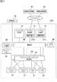
図1において、1は全体として本実施の形態によるストレージシステムを示す。このストレージシステム1は、データの入出力制御を行なうデータ入出力制御機能が搭載された記憶制御装置2と、複数のフラッシュメモリパッケージ13が収納された記憶装置3とを備えて構成される。(1) Configuration of Storage System According to this Embodiment (1-1) External Configuration of Storage System In FIG. 1, 1 indicates the overall storage system according to this embodiment. The
記憶制御装置2は、直方体形状のラックフレーム10内に、それぞれ複数の冷却ファンユニット11、ハードディスクドライブユニット12、フラッシュメモリパッケージ13及び論理基板14と、電源バッテリユニット15とが複数収容されて構成される。 The
冷却ファンユニット11は、1又は複数のファンを内蔵するユニットであり、フラッシュメモリパッケージ13や、ハードディスクドライブユニット12及び論理基板14等において発生した熱をラックフレーム10の外部に排出するために用いられる。 The
ハードディスクドライブユニット12は、所定大きさの筐体に例えば3.5インチのハードディスクドライブが収納されて構成される。かかる筐体の後端部側にはコネクタ(図示せず)が設けられており、このコネクタをラックフレーム10内に配置されたバックボード(図示せず)上のコネクタ(図示せず)に嵌め合わせることにより、当該ハードディスクドライブユニット12をバックボードに物理的及び電気的に接続した状態に装填することができるようになされている。 The hard
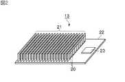
フラッシュメモリパッケージ13は、例えば図2に示すように、それぞれ複数のフラッシュメモリチップ20が実装された複数のフラッシュメモリモジュール(以下、フラッシュメモリとよぶ)21が、所定大きさの配線基板22上に交換自在に装着されて構成される。この配線基板22の一端側にはフラッシュメモリ制御LSI(Large Scale Integration circuit)23が実装されており、このフラッシュメモリ制御LSI23内に形成された後述のフラッシュメモリ制御部33によって、そのフラッシュメモリパッケージ13内の各フラッシュメモリチップ20に対するデータの入出力を制御し得るようになされている。 For example, as shown in FIG. 2, the
またフラッシュメモリパッケージ13の後端部側にはコネクタ(図示せず)が設けられており、このコネクタをラックフレーム10内に配置されたバックボード(図示せず)上の対応するコネクタに嵌め合わせることによって、当該フラッシュメモリパッケージ13をバックボードに物理的及び電気的に接続した状態に装填することができるようになされている。 Further, a connector (not shown) is provided on the rear end side of the
論理基板14は、図3で後述するチャネル制御部31、ディスク制御部32、キャッシュメモリ34、キャッシュ制御部35、接続部36、プロセッサ制御部37等が形成されて構成される。これら論理基板14は、ラックフレーム10内に配置されたバックボード(図示せず)に挿抜自在に接続されており、このバックボードを介してラックフレーム10内に装填された他の論理基板14等と通信を行なえるように構成されている。 The logical board 14 includes a
電源バッテリユニット15は、電源ユニット部15A及びバッテリユニット部15Bから構成される。このうち電源ユニット部15Aは、外部から供給される商用交流電力を直流電力に変換し、これを記憶制御装置2内の各部位にそれぞれ供給する。またバッテリユニット部15Bは、停電時や電源ユニット部15Aの異常時に、記憶制御装置2内の各部位に電力を供給するための予備電源として用いられる。 The
ラックフレーム10は、その内部が仕切り板によって複数段に区分けできるように構成されている。本実施の形態においては、ラックフレーム10内が全部で9段に区分けされており、その最上段及び上から6段目に冷却ファンユニット11、上から2段目及び3段目にハードディスクユニット12、上から4段目及び5段目にフラッシュメモリパッケージ13、上から7段目及び8段目に論理基板14、最下段に電源バッテリユニット15がそれぞれ収納されている。 The
一方、記憶装置3は、ラックフレーム16内に、冷却ファンユニット11、複数のフラッシュメモリパッケージ13及び電源バッテリユニット15が収容されて構成される。この記憶装置3は、ファイバーチャネル(Fibre channel)などからなる通信ケーブル(図示せず)を介して記憶制御装置2と接続されており、これにより記憶制御装置2内の論理基板14が通信ケーブルを介して記憶装置3に搭載された各フラッシュメモリパッケージ13と通信を行なえるように構成されている。 On the other hand, the
ラックフレーム16は、記憶制御装置2のラックフレーム11とほぼ同様の構成を有する。本実施の形態においては、ラックフレーム16内が全部で8段に区分けされており、その最上段に冷却ファンユニット11、最下段に電源バッテリユニット15がそれぞれ収納され、これら最上段及び最下段以外の各段部にそれぞれフラッシュメモリパッケージ13が収納されている。 The
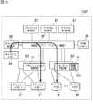
(1−2)ストレージシステムの内部構成
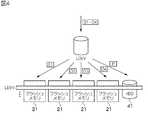
図3は、本実施の形態によるストレージシステム1の内部構成を示す。この図3に示すように、ストレージシステム1は、チャネル制御部31、ハードディスクドライブ41、ディスク制御部32、フラッシュメモリ20、フラッシュメモリ制御部33、キャッシュメモリ34、キャッシュ制御部35、接続部36、プロセッサ制御部37及び共有メモリ38を備えて構成される。(1-2) Internal Configuration of Storage System FIG. 3 shows the internal configuration of the
チャネル制御部31は、情報処理装置30との間のインタフェースとして機能し、当該情報処理装置30との間で各種コマンドやデータを送受する。また、チャネル制御部31は、情報処理装置30からのデータに基づいてパリティデータを生成するための演算回路310を備える。演算回路310の構成は後述で説明する。 The
ハードディスクドライブ41は、第2記憶デバイスであって、上述のようにハードディスクドライブユニット12内に収納された状態でストレージシステム1に搭載され、プロセッサ制御部37によりRAID方式で運用される。ハードディスクドライブ41としては、例えばSCSI(Small Computer System Interface)ディスク等の高価なハードディスクドライブや、SATA(Serial AT Attachment)ディスク等の安価なハードディスクが適用される。 The
ディスク制御部32は、第2記憶デバイス制御部であって、例えばファイバーチャネルケーブルを介して記憶制御装置2及び記憶装置3にそれぞれ搭載された各ハードディスクドライブと接続されている。ディスク制御部32は、これらハードディスクドライブ41に対するインタフェースとして機能し、ハードディスクドライブ41に対するデータの入出力を制御する。 The
フラッシュメモリ21は、第1記憶デバイスであって、書き換え可能な不揮発性の半導体メモリのグループであり、上述のようにフラッシュメモリパッケージ13としてストレージシステム1に搭載される。 The
複数のフラッシュメモリ20、及び、1又は複数のハードディスクドライブ41により複数のパリティグループPGが形成され、このパリティグループPGが提供する物理的な記憶領域上に1つの論理的なボリューム(以下、これを論理ボリュームと呼ぶ)LDEVが設定される。パリティグループPGとは、同一のパリティデータを共有するデータ群と、そのデータ群から算出されるパリティデータと、のグループをいう。 A plurality of parity groups PG are formed by a plurality of
図4には、論理ボリュームを形成させる一例を示している。本実施の形態では、データD1−D4と後述する演算回路310によって演算され、算出されたパリティデータPとは、複数のフラッシュメモリ21と少なくとも1台のハードディスクドライブ41が提供する物理的な記憶領域上に形成される論理ボリュームLDEVに格納される。パリティデータPは、上位装置である情報処理装置からのデータD1−D4を保護するためのデータであって、データD1−D4のうちいずれかのデータが消失した場合にも、消失したデータを復旧させるために使用するデータのことをいう。 FIG. 4 shows an example of forming a logical volume. In this embodiment, the data D1-D4 and the parity data P calculated and calculated by the
そして、情報処理装置30からのデータD1−D4は、論理ボリュームLDEVと対応付けられている複数のフラッシュメモリ21に格納され、パリティデータPは、論理ボリュームLDEVと対応付けられているハードディスクドライブ41に格納される。 Data D1 to D4 from the
情報処理装置30からのデータD1−D4及びパリティデータPは、この論理ボリュームLDEVに、フラッシュメモリ21上及びハードディスクドライブ41上のデータ管理単位である所定大きさのブロックを単位として読み書きされる。 Data D1-D4 and parity data P from the
各論理ボリュームLDEVには、それぞれ固有の識別番号(LUN:Logical Unit Number)が割り当てられる。そしてデータの入出力は、このLUNと、各ブロックにそれぞれ割り当てられるそのブロックに固有のブロック番号とを組み合わせたものをアドレスとして、当該アドレスを指定して行われる。 Each logical volume LDEV is assigned a unique identification number (LUN: Logical Unit Number). Data input / output is performed by designating the address using a combination of the LUN and a block number specific to the block assigned to each block as an address.
フラッシュメモリ制御部33は、第1記憶デバイス制御部であって、上述のように各フラッシュメモリパッケージ13にそれぞれ実装されたフラッシュメモリ制御LSI23内に形成される。フラッシュメモリ制御部33は、フラッシュメモリ21に対するインタフェースとして機能し、同じフラッシュメモリパッケージ13内の各フラッシュメモリ21に対するデータの入出力を制御する。 The flash
キャッシュメモリ34は、例えばSDRAM(Synchronous Dynamic Random Access Memory)等の揮発メモリから構成される。またキャッシュ制御部35は、キャッシュメモリ34に対するデータの入出力を制御する。 The
接続部36は、例えば相互接続可能なスイッチ又はバス等で構成される。チャネル制御部31、ディスク制御部32、フラッシュメモリ制御部33、キャッシュ制御部35、プロセッサ制御部37及び共有メモリ38間のデータやコマンドの授受は、この接続部36を介して行われる。 The
共有メモリ38は、チャネル制御部31、ディスク制御部32及びフラッシュメモリ制御部33により共有される記憶メモリである。共有メモリ38は、主にストレージシステム1の電源投入時に論理ボリュームLDEVから読み出されたシステム構成情報及び各種制御プログラムや、情報処理装置30からのコマンドなどを記憶するために利用される。 The shared
また、共有メモリ38には、図5に示すように、管理テーブル380、情報処理装置30からのデータを論理ボリュームLDEVに書き込むためのライトプログラム381、情報処理装置30に要求されたデータを論理ボリュームLDEVから読み出すためのリードプログラム382、及び、障害が生じた場合に消失したデータを回復させるためのコピーコレクションプログラム383、が格納される。 Further, as shown in FIG. 5, the shared
管理端末40は、例えば、CPU(図示せず)、メモリ(図示せず)及び康住する管理画面SC1等のハードウェア資源を備えるコンピュータシステムである。管理者は、管理端末40を入力操作することにより、ストレージシステム1を管理するためのコマンドをストレージシステム1に送信する。ストレージシステム1を管理するためのコマンドとしては、例えば、ハードディスクドライブ41の増設或いは減設、又はRAID構成の変更を指示するためのコマンド、ストレージシステム1の動作状態の確認や故障部位を特定するためのコマンド等がある。 The
なお、本実施の形態によるストレージシステム1では、冗長性をもたせるため、ディスク制御部32及びフラッシュメモリ制御部33がそれぞれ2つずつ設けられている。 In the
また、本実施の形態では、フラッシュメモリ制御部33とフラッシュメモリ21とのインタフェース、及び、ハードディスク制御部32とハードディスクドライブ41とのインタフェースには、SASを使用する。 In the present embodiment, SAS is used for the interface between the flash
(1−3)管理テーブルの構成
それでは次に、共有メモリ38に格納される管理テーブル380について説明する。(1-3) Configuration of Management Table Next, the management table 380 stored in the shared
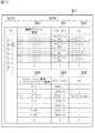
図6に示すように、管理テーブル380は、フラッシュメモリ21に情報処理装置30からのデータを格納し、ハードディスクドライブ41にパリティデータPを格納するよう管理するためのテーブルである。この管理テーブル380は、管理端末40の画面上に出力される。 As shown in FIG. 6, the management table 380 is a table for managing data stored from the
管理テーブル380は、「データ名」欄3810、そのデータをキャッシュメモリ34上に一時的に格納したアドレスを示す「メモリアドレス」欄3811、及び、そのデータの長さを示す「データ長」欄3812、「パリティグループ番号」欄3813、「論理ボリューム番号」欄3814、「フラッシュメモリ番号/ハードディスクドライブ番号」欄3815、及び「アドレス」欄3816から構成される。 The management table 380 includes a “data name”
「パリティグループ番号」欄3813では、そのデータが所属するパリティグループPGの番号が登録される。 In the “parity group number”
「論理ボリューム番号」欄3814では、そのデータを格納する論理ボリュームLDEVの番号が登録される。 In the “logical volume number”
また、「フラッシュメモリ番号/ハードディスクドライブ番号」欄3815では、そのデータを格納する論理ボリュームLDEVと対応付けされ、且つ、実際にデータを格納するフラッシュメモリ番号又はハードディスクドライブ番号が登録される。 In the “flash memory number / hard disk drive number”
そして、「アドレス」欄3816は、そのデータを格納したフラッシュメモリ21内又はハードディスクドライブ41内のアドレスが登録される。 In the “address”
(1−4)ライト処理
ではどのようにデータをフラッシュメモリ21に格納し、パリティデータPをハードディスクドライブ41に格納するかというライト処理について説明する。ライト処理は、プロセッサ制御部37がライトプログラム621に基づいて実行する。(1-4) Write Process Now, a write process of how data is stored in the
図7は、ストレージシステム1内でのライト処理を示すフローチャートである。 FIG. 7 is a flowchart showing write processing in the
まず、プロセッサ制御部37は、情報処理装置30からのデータ(以下、ホストデータ)D1−D4をキャッシュメモリに格納後、情報処理装置30に完了報告を通知するとライトプログラム621を起動させて、ライト処理を開始する(S0)。 First, after storing data (hereinafter referred to as host data) D1-D4 from the
次にプロセッサ制御部37は、キャッシュ制御部35にホストデータを読み出す旨のリード要求を発行する(S1)。そうすると、キャッシュ制御部35がキャッシュメモリからホストデータを読み出し、キャッシュ制御部35がホストデータD1−D4をプロセッサ制御部37に送信する(S2)。 Next, the
ホストデータD1−D4を受信したプロセッサ制御部37は、このホストデータD1−D4に対するパリティデータPを演算回路310で演算し、生成する(S3)。演算回路310での演算の説明は後述する。その後、プロセッサ制御部37は、チャネル制御部31で演算したパリティデータPをキャッシュ制御部35に送信する(S4)。そうすると、キャッシュ制御部35がキャッシュメモリ34に演算したパリティデータPを格納する(S5)。同時に、プロセッサ制御部37は、演算したパリティデータPを管理テーブル620に登録する。 Upon receiving the host data D1-D4, the
プロセッサ制御部37は、フラッシュメモリ制御部33に対してホストデータD1−D4をフラッシュメモリ21に書き込む旨、及び、ディスク制御部32に対してパリティデータをハードディスクドライブ41に書き込む旨のライト要求を発行する(S6)。 The
フラッシュメモリ制御部33は、管理テーブル620を参照し、キャッシュ制御部35にホストデータD1−D4を読み出す旨のリード要求を発行する(S7)。そうするとキャッシュ制御部35は、ホストデータD1−D4をキャッシュメモリ34から読み出して(S8)、フラッシュメモリ制御部35に読み出したホストデータD1−D4を送信する(S9)。その後、フラッシュメモリ制御部35は、読み出したホストデータD1−D4を複数のフラッシュメモリ21に格納し(S10)、管理テーブルの該当する箇所にホストデータに関する情報を登録する。 The flash
また、プロセッサ制御部37は、管理テーブル620を参照し、キャッシュ制御部35にパリティデータPを読み出すように、リード要求を発行する(S11)。そうするとキャッシュ制御部35は、パリティデータPをキャッシュメモリ34から読み出して(S12)、ディスク制御部35に読み出したパリティデータPを送信する(S13)。ディスク制御部35がハードディスクドライブ41にパリティデータPを格納し(S14)、管理テーブルの該当する箇所にパリティデータPに関する情報を登録する。 Further, the
プロセッサ制御部37は、フラッシュメモリ制御部33から完了報告を受信し(S15)、ディスク制御部32から完了報告を受信すると(S16)、ライト処理を終了する(S17)。 The
ここで、図8に示すように、1台のハードディスクドライブ41の記憶領域にパリティデータPを保存するのではなく、複数台のハードディスクドライブ41の記憶領域にパリティデータP1−P3を保存する構成を用いてもよい。この場合、図9に示すように、1台のハードディスクドライブがビジー状態にも関わらず、相次いでパリティデータを書き込もうとすると、最初のパリティデータの書き込み処理が終了して次のパリティデータの書き込み処理が開始される時間が遅延する。しかし、図8及び図10に示すように、複数台のハードディスクドライブ41をRAID構成にすれば、1台のハードディスクドライブ41がビジー状態であっても、他のハードディスクドライブ41には影響を及ぼさないため、パリティデータP1−P3の書き込みが円滑に行える。加えて、パリティデータPをパリティデータP1−P3に分散して複数のハードディスクドライブ41に格納するため、パリティデータP1−P3の書き込む時間が短縮され、ライト性能の向上を図ることができる。 Here, as shown in FIG. 8, the parity data P1 to P3 are stored in the storage areas of the plurality of hard disk drives 41, instead of storing the parity data P in the storage area of one
また、図11に示すように、パリティデータP4−P6を1台のハードディスクドライブ41に集中して格納するのではなく、複数台のハードディスクドライブ41を用意して、パリティデータP4−P6が生成されるたびに異なるハードディスクドライブ41に格納する構成を用いてもよい。この構成によっても、1台のハードディスクドライブ41がビジー状態であっても、他のハードディスクドライブ41には影響を及ぼさないため、パリティデータP4−P6の書き込みが円滑に行える。 In addition, as shown in FIG. 11, the parity data P4-P6 is generated by preparing a plurality of hard disk drives 41 instead of storing the parity data P4-P6 in one
このようにライト処理の場合には、本実施の形態のストレージシステムは、ホストデータをフラッシュメモリに格納し、パリティデータをハードディスクドライブに格納するように振り分けることができる。これにより、リードレスポンスの速いフラッシュメモリからデータを読み出せ、データを更新する度に書き込まれるパリティデータは書き込み回数の制限がないハードディスクを使用することで、システムの性能が向上する。特に、RAID3はパリティデータを1台のハードディスクドライブに固定して格納するため、RAID3を構築するストレージシステムにはもっとも有効である。 As described above, in the case of write processing, the storage system according to the present embodiment can distribute host data in a flash memory and parity data in a hard disk drive. As a result, data can be read from the flash memory with a fast read response, and the parity data written each time the data is updated uses a hard disk with no limit on the number of writes, thereby improving the system performance. In particular,
(1−5)演算処理
それでは具体的にどのように演算回路310でパリティデータPを演算し、算出するのかという演算処理について説明する。図12は演算回路310の構成図である。(1-5) Arithmetic Processing Now, the arithmetic processing of how to calculate and calculate the parity data P by the
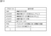
演算回路310は、チャネル制御部31が保持する回路であって、プロセッサ制御部37からのパラメータに従って演算回路310内の各部に指示を行うパラメータ制御部311、演算や実行状態の保持に用いられるレジスタ312、実際に演算を実行する演算論理部313、及び、演算した値を一時的に保存するバッファ・メモリ314から主に構成されている。 The
ここでパラメータの内容を、図13に示す。例えば、パラメータ「CMD」は、演算方式の内容を定義している。具体的な「CMD」の内容としては、パリティデータを生成する指示、パーシャルライトを生成する指示、消失データのコレクト指示、が挙げられる。 The contents of the parameters are shown in FIG. For example, the parameter “CMD” defines the content of the calculation method. Specific contents of “CMD” include an instruction to generate parity data, an instruction to generate partial write, and an instruction to collect lost data.
なお、パーシャルライトとは、あるデータが更新したことに伴って新たなパリティデータを演算することをいう。また、消失データのコレクトとは、あるデータが消失した等で障害が発生した場合に、他のデータとパリティデータとから消失したデータを演算することをいう。 Note that the partial write means that new parity data is calculated when certain data is updated. Further, the lost data collection refers to calculating lost data from other data and parity data when a failure occurs due to loss of certain data.
また、図表の内容としては、パラメータ「CCMADR」は、演算元のデータを読み出すアドレスが指示され、パラメータ「NCMADR」は、演算後のデータの書き込みアドレスが指示される。パラメータ「LENGTH」は、読み込むデータ長が指示され、パラメータ「STSADR」は演算の終了が指示される。パラメータ「PRM」は、パティデータの演算の際に用いられる関数の係数が指示され、パラメータ「LRC」はパラメータ「CMD」が正しいか否かを判断するために保証コードの付与が指示される。なお、列挙したパラメータに限られず、演算に必要なパラメータは適宜設定されるものとする。 Further, as the contents of the chart, the parameter “CCMADR” is instructed an address for reading out the data of the operation source, and the parameter “NCMADR” is instructed the write address of the data after the operation. The parameter “LENGTH” indicates the data length to be read, and the parameter “STSADR” indicates the end of the calculation. The parameter “PRM” is instructed by a coefficient of a function used when calculating the patty data, and the parameter “LRC” is instructed to give a guarantee code to determine whether the parameter “CMD” is correct. Note that the parameters necessary for the calculation are not limited to the enumerated parameters and are appropriately set.
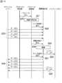
それでは、どのようにパリティデータを生成するかについて、具体的に説明する。図14は、パリティデータを演算するためのフローチャートである。 Now, how to generate parity data will be specifically described. FIG. 14 is a flowchart for calculating parity data.
プロセッサ制御部37からパラメータ「CMD」が書き込まれると(S20)、演算回路310が起動する(S21)。演算回路310のパラメータ制御部311は、パラメータ「CCMADR」を発行し、キャッシュメモリ34上のホストデータD1−D4を演算論理部313に読み出すよう指示をする(S22)。そうすると、演算論理部313がキャッシュメモリ34上のホストデータをキャッシュメモリ34から読み出す(S23)。 When the parameter “CMD” is written from the processor control unit 37 (S20), the
引き続きパラメータ制御部311は、パラメータ「PRM」等の演算に必要なパラメータを発行して、演算論理部313に演算制御をするよう指示をすると(S24)、演算論理部313は、ホストデータD1−D4のパリティデータPを演算する(S25)。パラメータ制御部311は、演算したパリティデータPを、バッファ・メモリ314に一時的に格納する(S26)。 Subsequently, when the
パラメータ制御部311は、パラメータ「NCMADR」を発行し、読み込んだホストデータD1−D4と演算したパリティデータPとをキャッシュメモリ34に書き戻すよう指示をする(S27)。そうすると、演算論理部313が読み込んだホストデータD1−D4と演算したパリティデータPとをキャッシュメモリ34に書き戻して(S28、S29)、演算処理を終了する。 The
ここで、図15に示すストレージシステム100のように、演算回路320はディスク制御部32が保持してもよい。この場合には、キャッシュメモリ34からデータの読み出しを、ディスク制御部32とフラッシュメモリ制御部33とに、2回行わなければならないが、情報処理装置30とチャネル制御部31との間のトランザクションに影響を与えなくて済む。 Here, as in the
また、図16に示すストレージシステム100´のように、演算回路320はディスク制御部32が保持しつつ、さらにブロードキャスト機能をもつ接続部36´の構成としてもよい。この場合には、接続部36´がキャッシュメモリ34から読み出したデータをディスク制御部32とフラッシュメモリ制御部33とに送信することができるので、キャッシュメモリ34からデータの読み出しを複数回行う必要がない。このため、情報処理装置30とチャネル制御部31との間だけではなく、キャッシュメモリ34と接続部36´との間のトランザクションに影響を与えなくて済む。 Further, as in the
(1−6)リード処理
では次に、どのようにデータをフラッシュメモリ21から読み出すかというリード処理について説明する。リード処理は、プロセッサ制御部37がリードプログラム622に基づいて実行する。(1-6) Read Process Next, a read process for reading data from the
図17は、ストレージシステム1内でのリード処理を示すフローチャートである。 FIG. 17 is a flowchart showing read processing in the
まず、プロセッサ制御部37は、情報処理装置30から、あるデータDの取得要求を受信すると(S30)、リード処理を開始する(S31)。 First, when receiving an acquisition request for certain data D from the information processing apparatus 30 (S30), the
次にプロセッサ制御部37は、管理テーブルを参照して、データを読み出すフラッシュメモリと読み出しアドレスとを確認する(S32)。確認後、プロセッサ制御部37は、データを読み出すフラッシュメモリ21と読み出しアドレスとの指示をフラッシュメモリ制御部に送信する(S33)。 Next, the
プロセッサ制御部37からの指示を受信したフラッシュメモリ制御部33は、指定されたフラッシュメモリ21のアドレスから、情報処理装置30が要求するデータを読み出す(S34)。その後、プロセッサ制御部37は、読み出したデータを、キャッシュメモリに一時的に格納する。 The flash
プロセッサ制御部37は、キャッシュメモリ34に格納したデータを、情報処理装置30に送信するように、チャネル制御部に指示をする(S35)。 The
チャネル制御部31は、キャッシュメモリ34に格納したデータを、情報処理装置30に送信すると(S36)、プロセッサ制御部37に送信完了報告を行う(S37)。プロセッサ制御部37は、送信完了報告を受け取ると、リード処理を終了する(S38)。 When the data stored in the
このようにリード処理の場合には、ハードディスクドライブ41に格納されたパリティデータPを読み出す必要はなく、リードレスポンスの速いフラッシュメモリ21からデータを読み出せば足りるので、リードレスポンスがフラッシュメモリ21より遅いハードディスドライブ41を使用する必要がない。 Thus, in the case of read processing, it is not necessary to read out the parity data P stored in the
(1−7)コレクションコピー処理
次に、コレクションコピー処理について説明する。コレクションコピーとは、図18の概念図に示すように、あるデータが消失した等で障害が発生した場合に、他のデータとパリティデータとから消失したデータを演算し、スペアのフラッシュメモリに演算後のデータを格納する(コピーする)処理をいう。(1-7) Collection Copy Processing Next, collection copy processing will be described. As shown in the conceptual diagram of FIG. 18, the collection copy calculates lost data from other data and parity data when a failure occurs due to loss of certain data, etc., and calculates to a spare flash memory. The process of storing (copying) later data.
コレクションコピー処理は、プロセッサ制御部37がコレクションコピープログラム623に基づいて実行する。 The collection copy process is executed by the
具体的には、管理者が、データが消失したフラッシュメモリ21を管理端末40の管理画面で確認すると、管理者がストレージシステム1に対してコレクションコピーの指示を出す。この指示を受けたプロセッサ制御部37が、コレクションコピー処理を開始する。 Specifically, when the administrator confirms the
ここで、管理画面について説明する。 Here, the management screen will be described.
図19は、データを消失した等で障害が発生した場合のフラッシュメモリ21又はハードディスクドライブ41を管理者に通知する画面SC1を示す。 FIG. 19 shows a screen SC1 for notifying the administrator of the
障害が発生すると、フラッシュメモリ制御部33又はディスク制御部32が障害を検出し、プロセッサ制御部37に通知する。通知を受けたプロセッサ制御部37が、管理端末40に、障害が発生したフラッシュメモリ21の情報、又は、障害が発生したハードディスクドライブ41の情報を送信する。管理端末40を管理する管理者が、管理画面SC1に基づいて、障害が発生した情報を確認することができる。 When a failure occurs, the flash
画面左欄SC10には、ストレージシステム1内に構成される全てのパリティグループPGの番号が表示される。障害が発生した場合には、障害が発生したパリティグループ番号を点滅させる等で、管理者に視覚的に通知する。 In the left column SC10 of the screen, the numbers of all parity groups PG configured in the
そして、画面右欄SC20には、画面左欄S10で選択したパリティグループPG2に所属するフラッシュメモリ21の情報やハードディスクドライブ41の情報が表示される。画面右欄SC20は、例えば、上段には障害が発生した論理構成の情報、下段には障害が発生した物理構成の情報、が表示される。 In the screen right column SC20, information on the
論理構成の情報としては、障害が発生している「論理ボリューム番号」欄200、その論理ボリュームLDEVは回復しているかのコレクション要否を示す「ステータス」欄201、及び、その論理ボリュームLDEVに関する管理情報等を示す「etc」欄203がある。 The logical configuration information includes a “logical volume number”
物理構成の情報としては、「フラッシュメモリ番号又はハードディスクドライブ番号」欄203、その物理デバイス番号がどの筐体の何段目かを示す「ロケーション」欄204、及び、その物理デバイス番号は回復しているかのコレクション要否を示す「etc」欄205がある。 As physical configuration information, the “flash memory number or hard disk drive number”
なお、これらの構成情報は一例であるので、上述した構成情報には限られない。 Note that these pieces of configuration information are examples, and are not limited to the configuration information described above.
障害が発生した場合には、障害が発生したフラッシュメモリ21の情報又はハードディスクドライブ41の情報を点滅させる等で、管理者に視覚的に通知する。 When a failure occurs, the administrator is visually notified by blinking the information of the
それでは、具体的なコピーコレクション処理について説明する。図20は、コピーコレクション処理を示すフローチャートである。 Now, specific copy collection processing will be described. FIG. 20 is a flowchart showing copy collection processing.
管理端末40からのコレクションコピー指示をストレージシステム1で受信すると(S40)、プロセッサ制御部37がコレクションコピー処理を開始する(S41)。本実施の形態では、フラッシュメモリ21の1つに障害が発生した場合について説明する。 When the
プロセッサ制御部37は、データを消失したフラッシュメモリ21以外のフラッシュメモリ21からデータD1、D2、D4を読み出すようフラッシュメモリ制御部33に指示を送信し(S42)、データを消失したフラッシュメモリ21が所属するパリティグループPGと同じパリティグループPGを持つパリティデータPを読み出すようディスク制御部32に指示を送信する(S43)。 The
フラッシュメモリ制御部33は、データを消失したフラッシュメモリ21が所属するパリティグループPGを持つその他のフラッシュメモリ21からデータD1、D2、D4をキャッシュメモリ34に読み出す(S44)。また、ディスク制御部32は、データを消失したフラッシュメモリ21が所属するパリティグループPGと同じパリティグループPGを持つハードディスクドライブ41からパリティデータPをキャッシュメモリ34に読み出す(S45)。 The flash
その後、プロセッサ制御部37は、パラメータ「CMD」を演算回路310に書き込むと、消失したデータの演算処理を行う。パラメータ「CMD」の具体的な内容は、消失データのコレクトである。演算回路310のパラメータ制御部311が、キャッシュメモリ34上のデータD1、D2、D4とパリティデータPとを読み出し(S46)、演算ステップS22からS28に従って、消失したデータの演算を行う(S47)。 After that, when the parameter “CMD” is written in the
なお、ステップS23とステップS28では、データD3をキャッシュメモリ34から読み出しているが、コピーコレクション処理においては、消失したデータD3は読み出さずに、パリティデータPを読み出すものとする。また、ステップS26では、演算したパリティデータPをバッファ・メモリ314に格納しているが、コピーコレクション処理においては、演算したデータD3を格納するものとする。 In step S23 and step S28, the data D3 is read from the
演算回路310は、データを再構築させると、バッファ・メモリ314に一時的に格納する。そして演算回路310は、再構築したデータをバッファ・メモリ314から読み出して、キャッシュメモリ34に再構築したデータを送信して、演算処理を終了させる。 The
プロセッサ制御部37は、キャッシュメモリ34から再構築したデータを読み出し(S48)、スペア用のフラッシュメモリ21´に格納する(S49)。そしてプロセッサ制御部37は、再構築したデータに関する情報を管理テーブル620に登録すると、コピーコレクション処理を終了する(S50)。 The
(1−8)本実施の形態の効果
本実施の形態によれば、リードレスポンスの速いフラッシュメモリをストレージシステムに搭載し、フラッシュメモリの書き込み回数を制限することでシステムの寿命を延ばすことができる。(1-8) Effects of this Embodiment According to this embodiment, it is possible to extend the life of the system by mounting a flash memory with a fast read response in the storage system and limiting the number of times the flash memory is written. .
(2)第2の実施の形態
次に、第2の実施の形態によるストレージシステム200について以下に説明する。(2) Second Embodiment Next, a
(2−1)システム構成
本実施の形態によるストレージシステム200のシステム構成は、図21に示すように、第1の実施の形態のストレージシステム1で説明をしたフラッシュメモリ制御部33とディスク制御部32とを一体にしたフラッシュメモリ・ディスク制御部39を備える。(2-1) System Configuration As shown in FIG. 21, the system configuration of the
フラッシュメモリ・ディスク制御部39は、第3記憶デバイス制御部であって、フラッシュメモリ21に対してデータD1−D4の入出力を制御するとともに、ハードディスクドライブ41に対してパリティデータPの入出力を制御する。 The flash memory /
本実施の形態では、フラッシュメモリ・ディスク制御部39とフラッシュメモリ21、フラッシュメモリ・ディスク制御部39とハードディスクドライブ41とのインタフェースには、SASを使用する。フラッシュメモリ21とハードディスクドライブ41とのアクセスに同一のプロトコルを用いることで、制御部を一体とすることができる。これにより、ストレージシステム200を構築する際にかかるコストを削減でき、管理を簡易にすることができる。 In this embodiment, SAS is used as an interface between the flash memory /
ここで、図22に示すストレージシステム200´のように、演算回路390はフラッシュメモリ・ディスク制御部39´が保持してもよい。図15で説明をした第1の実施の形態の変形例では、キャッシュメモリ34からデータの読み出しを、ディスク制御部32とフラッシュメモリ制御部33とに、2回行わなければならなかった。しかし、本実施の形態の変形例では、ディスク制御部32とフラッシュメモリ制御部33とを一体化しているため、キャッシュメモリ34からデータの読み出しは1回で済む。ストレージシステム200´は、情報処理装置30とチャネル制御部31との間のトランザクションに影響を与える必要がない。 Here, as in the
なお、その他の構成要件は、第1の実施の形態で説明した構成要件と同じであるため、説明を省略する。第1の実施の形態で説明した構成と同じ構成には、第1の実施の形態で付与した図番と同一の図番を付与する。 Other configuration requirements are the same as the configuration requirements described in the first embodiment, and thus description thereof is omitted. The same figure number as the figure number assigned in the first embodiment is assigned to the same structure as that described in the first embodiment.
(2−2)ライト処理
では、どのようにデータD1−D4をフラッシュメモリ21に格納し、パリティデータPをハードディスクドライブ41に格納するのか、というライト処理について説明する。ライト処理は、プロセッサ制御部37がライトプログラム621に基づいて実行する。(2-2) Write Process Now, the write process of how to store the data D1-D4 in the
図23に示すように、プロセッサ制御部37は、ステップS60からステップS75までの処理をステップS0からステップS15までの処理と同様の手順で実行する。ただし、プロセッサ制御部37がフラッシュメモリ制御部33とディスク制御部32とのそれぞれに指示をしていたステップS6、ステップS9、及びステップS13においては、フラッシュメモリ・ディスク制御部39に一括して指示を出すものとする(S66、S69、S73)。 As shown in FIG. 23, the
プロセッサ制御部37は、フラッシュメモリ・ディスク制御部39から完了報告を受信すると(S75)、ライト処理を終了する(S76)。 When the
本実施の形態におけるライト処理は、プロセッサ制御部37が指示するデータの転送先アドレスが第1の実施の形態で説明をしたライト処理とは異なる。フラッシュメモリ・ディスク制御部39として一体にしても、ホストデータをフラッシュメモリに格納し、パリティデータをハードディスクドライブに格納するように振り分けることができる。これにより、リードレスポンスの速いフラッシュメモリからデータを読み出せ、データを更新する度に書き込まれるパリティデータは書き込み回数の制限がないハードディスクを使用することで、システムの性能が向上する。 The write processing in the present embodiment is different from the write processing described in the first embodiment in the data transfer destination address instructed by the
(2−3)本実施の形態の効果
本実施の形態によれば、リードレスポンスの速いフラッシュメモリをストレージシステムに搭載し、フラッシュメモリの書き込み回数を制限することでシステムの寿命を延ばすことができる。(2-3) Effects of this Embodiment According to this embodiment, a flash memory with a fast read response is mounted in a storage system, and the life of the system can be extended by limiting the number of times the flash memory is written. .
(3)その他の実施の形態
第1の実施の形態では、フラッシュメモリ制御部とフラッシュメモリとのインタフェース、及び、ディスク制御部とハードディスクドライブとのインタフェースには、SASを使用したが、フラッシュメモリ制御部とフラッシュメモリとのインタフェースにはSASを使用し、ディスク制御部とハードディスクドライブとのインタフェースにはファイバーチャネルを使用しても良い。ファイバーチャネルを使用すれば高性能なプロトコルを用いることができるので、ライト性能の向上を図ることができる。(3) Other Embodiments In the first embodiment, SAS is used for the interface between the flash memory control unit and the flash memory and the interface between the disk control unit and the hard disk drive. SAS may be used for the interface between the disk controller and the flash memory, and Fiber Channel may be used for the interface between the disk controller and the hard disk drive. If Fiber Channel is used, a high-performance protocol can be used, so that the write performance can be improved.
プロセッサ制御部がストレージシステム1内の各制御部に対して指示を出したが、これは一例であり、例えば、チャネル制御部31内のマイクロプロセッサが各制御部に対して指示をしてもよい。 The processor control unit issues an instruction to each control unit in the
第2の実施の形態では、フラッシュメモリ・ディスク制御部とフラッシュメモリとのインタフェース、及び、フラッシュメモリ・ディスク制御部とハードディスクドライブとのインタフェースには、SASを使用したが、フラッシュメモリとハードディスクドライブとのアクセスに同一のプロトコルを用いればよく、SASのインタフェースに限られない。 In the second embodiment, SAS is used for the interface between the flash memory / disk control unit and the flash memory and the interface between the flash memory / disk control unit and the hard disk drive. It is sufficient to use the same protocol for access, and it is not limited to the SAS interface.
本発明は、複数のストレージシステムや、その他の形態のストレージシステムに広く適用することができる。 The present invention can be widely applied to a plurality of storage systems and other forms of storage systems.
1、100、100´、200、200´……ストレージシステム、30……情報処理装置、31、31´……チャネル制御部、310、310´、390……演算回路、32……ディスク制御部、33……フラッシュメモリ制御部、34……キャッシュメモリ、35……キャッシュ制御部、36、36´……接続部、37……プロセッサ制御部、38……共有メモリ、380……管理テーブル、39……フラッシュメモリ・ディスク制御部、P……パリティデータ、D……データ、21、21´……フラッシュメモリ、41……ハードディスクドライブ。 1, 100, 100 ', 200, 200' ... Storage system, 30 ... Information processing device, 31, 31 '... Channel control unit, 310, 310', 390 ... Arithmetic circuit, 32 ... Disk control unit , 33... Flash memory control unit, 34... Cache memory, 35... Cache control unit, 36, 36 '.. connection unit, 37 .... processor control unit, 38 .. shared memory, 380. 39: Flash memory / disk control unit, P: Parity data, D: Data, 21, 21 ': Flash memory, 41: Hard disk drive.
Claims (10)
Translated fromJapanese前記第1記憶デバイスに対する前記データの入出力を制御する第1記憶デバイス制御部と、
前記データのパリティデータを算出する演算回路部と、
前記パリティデータが入出力される第2記憶デバイスと、
前記第2記憶デバイスに対する前記パリティデータの入出力を制御する第2記憶デバイス制御部と、を備え、
前記第1記憶デバイスは前記第2記憶デバイスよりリードアクセスの速い記憶デバイスであること
を特徴とするストレージシステム。A first storage device to which data from the host device is input and output;
A first storage device controller that controls input and output of the data to and from the first storage device;
An arithmetic circuit unit for calculating parity data of the data;
A second storage device to which the parity data is input and output;
A second storage device controller that controls input / output of the parity data to the second storage device,
The storage system, wherein the first storage device is a storage device having a faster read access than the second storage device.
ことを特徴とする請求項1記載のストレージシステム。The storage system according to claim 1, wherein the first storage device control unit and the second storage device control unit are physically integrated.
前記第2記憶デバイス制御部は、複数の前記第2記憶デバイスの記憶領域内に、前記演算回路により算出された前記パリティデータを分散して格納する
ことを特徴とする請求項1記載のストレージシステム。A plurality of the second storage devices are provided;
The storage system according to claim 1, wherein the second storage device control unit stores the parity data calculated by the arithmetic circuit in a storage area of a plurality of the second storage devices in a distributed manner. .
ことを特徴とする請求項1記載のストレージシステム。The storage system according to claim 1, wherein the arithmetic circuit unit is provided in the second storage device control unit.
ことを特徴とする請求項1記載のストレージシステム。The storage system according to claim 1, wherein the first storage device is a flash memory.
前記第1記憶デバイスに対する前記データの入出力を第1記憶デバイス制御部で制御するステップと、
前記データのパリティデータを演算回路部で算出するステップと、
前記パリティデータを第2記憶デバイスに格納するステップと、
前記第2記憶デバイスに対する前記パリティデータの入出力を第2記憶デバイス制御部で制御するステップと、
を備えることを特徴とするデータ保存方法。Inputting / outputting data from the host device to the first storage device having a faster read response than the second storage device;
Controlling the input / output of the data to and from the first storage device by a first storage device controller;
Calculating parity data of the data in an arithmetic circuit unit;
Storing the parity data in a second storage device;
Controlling the input and output of the parity data to and from the second storage device by a second storage device controller;
A data storage method comprising:
ことを特徴とする請求項6記載のデータ保存方法。The data storage method according to claim 6, wherein the first storage device control unit and the second storage device control unit are physically integrated.
前記第2記憶デバイス制御部では、複数の前記第2記憶デバイスの記憶領域内に、前記演算回路により算出された前記パリティデータを分散して格納するステップをさらに有する
ことを特徴とする請求項6記載のデータ保存方法。A plurality of the second storage devices are provided;
The second storage device control unit further includes a step of distributing and storing the parity data calculated by the arithmetic circuit in a storage area of a plurality of the second storage devices. The data storage method described.
ことを特徴とする請求項6記載のデータ保存方法。The data storage method according to claim 6, wherein the arithmetic circuit unit is provided in the second storage device control unit.
ことを特徴とする請求項6記載のデータ保存方法。The data storage method according to claim 6, wherein the first storage device is a flash memory.
Priority Applications (2)
| Application Number | Priority Date | Filing Date | Title |
|---|---|---|---|
| JP2008085776AJP2009238094A (en) | 2008-03-28 | 2008-03-28 | Storage system and data storage method |
| US12/155,207US8103939B2 (en) | 2008-03-28 | 2008-05-30 | Storage system and data storage method |
Applications Claiming Priority (1)
| Application Number | Priority Date | Filing Date | Title |
|---|---|---|---|
| JP2008085776AJP2009238094A (en) | 2008-03-28 | 2008-03-28 | Storage system and data storage method |
Publications (1)
| Publication Number | Publication Date |
|---|---|
| JP2009238094Atrue JP2009238094A (en) | 2009-10-15 |
Family
ID=41119000
Family Applications (1)
| Application Number | Title | Priority Date | Filing Date |
|---|---|---|---|
| JP2008085776APendingJP2009238094A (en) | 2008-03-28 | 2008-03-28 | Storage system and data storage method |
Country Status (2)
| Country | Link |
|---|---|
| US (1) | US8103939B2 (en) |
| JP (1) | JP2009238094A (en) |
Cited By (5)
| Publication number | Priority date | Publication date | Assignee | Title |
|---|---|---|---|---|
| WO2011045916A1 (en) | 2009-10-15 | 2011-04-21 | キヤノン株式会社 | Electrificating member and electrophotographic device |
| JP2011159150A (en)* | 2010-02-02 | 2011-08-18 | Nec Corp | Disk array device and data control method |
| JP2012038212A (en)* | 2010-08-10 | 2012-02-23 | Nec Corp | Storage device and control method thereof |
| JP2013142912A (en)* | 2012-01-06 | 2013-07-22 | Nec Corp | Disk array control device, disk array device, and disk array control method |
| JP2021009646A (en)* | 2019-07-03 | 2021-01-28 | 富士通株式会社 | Storage controller and storage control program |
Families Citing this family (8)
| Publication number | Priority date | Publication date | Assignee | Title |
|---|---|---|---|---|
| WO2009062029A1 (en)* | 2007-11-09 | 2009-05-14 | Carnegie Mellon University | Efficient high performance system for writing data from applications to a safe file system |
| US8806300B2 (en)* | 2009-05-25 | 2014-08-12 | Hitachi, Ltd. | Storage subsystem |
| US8468423B2 (en)* | 2011-09-01 | 2013-06-18 | International Business Machines Corporation | Data verification using checksum sidefile |
| US9043538B1 (en)* | 2013-12-30 | 2015-05-26 | Nationz Technologies Inc. | Memory system and method for controlling nonvolatile memory |
| JP6818982B2 (en) | 2015-06-01 | 2021-01-27 | エスゼット ディージェイアイ テクノロジー カンパニー リミテッドSz Dji Technology Co.,Ltd | How to store files |
| US10733118B2 (en)* | 2016-08-24 | 2020-08-04 | Hitachi, Ltd. | Computer system, communication device, and storage control method with DMA transfer of data |
| US10481803B2 (en) | 2017-06-16 | 2019-11-19 | Western Digital Technologies, Inc. | Low write overhead consensus protocol for distributed storage |
| US10289489B2 (en)* | 2017-07-11 | 2019-05-14 | Western Digital Technologies, Inc. | Update efficient consensus protocols for erasure coded data stores |
Family Cites Families (11)
| Publication number | Priority date | Publication date | Assignee | Title |
|---|---|---|---|---|
| US5307356A (en)* | 1990-04-16 | 1994-04-26 | International Business Machines Corporation | Interlocked on-chip ECC system |
| US6701480B1 (en)* | 2000-03-08 | 2004-03-02 | Rockwell Automation Technologies, Inc. | System and method for providing error check and correction in memory systems |
| US7225308B2 (en)* | 2003-10-30 | 2007-05-29 | International Business Machines Corporation | Inexpensive reliable computer storage via hetero-geneous architecture and a staged storage policy |
| US7234074B2 (en)* | 2003-12-17 | 2007-06-19 | International Business Machines Corporation | Multiple disk data storage system for reducing power consumption |
| US7136973B2 (en)* | 2004-02-04 | 2006-11-14 | Sandisk Corporation | Dual media storage device |
| JP5008845B2 (en) | 2005-09-01 | 2012-08-22 | 株式会社日立製作所 | Storage system, storage apparatus and control method thereof |
| JP4933211B2 (en)* | 2006-10-10 | 2012-05-16 | 株式会社日立製作所 | Storage device, control device, and control method |
| US8019938B2 (en)* | 2006-12-06 | 2011-09-13 | Fusion-I0, Inc. | Apparatus, system, and method for solid-state storage as cache for high-capacity, non-volatile storage |
| US7865761B1 (en)* | 2007-06-28 | 2011-01-04 | Emc Corporation | Accessing multiple non-volatile semiconductor memory modules in an uneven manner |
| US8122322B2 (en)* | 2007-07-31 | 2012-02-21 | Seagate Technology Llc | System and method of storing reliability data |
| US20110208933A1 (en)* | 2008-10-27 | 2011-08-25 | Kaminario Technologies Ltd. | Mass-Storage System Utilizing Solid-State Storage and Non-Solid-State Storage |
- 2008
- 2008-03-28JPJP2008085776Apatent/JP2009238094A/enactivePending
- 2008-05-30USUS12/155,207patent/US8103939B2/ennot_activeExpired - Fee Related
Cited By (7)
| Publication number | Priority date | Publication date | Assignee | Title |
|---|---|---|---|---|
| WO2011045916A1 (en) | 2009-10-15 | 2011-04-21 | キヤノン株式会社 | Electrificating member and electrophotographic device |
| JP2011159150A (en)* | 2010-02-02 | 2011-08-18 | Nec Corp | Disk array device and data control method |
| JP2012038212A (en)* | 2010-08-10 | 2012-02-23 | Nec Corp | Storage device and control method thereof |
| JP2013142912A (en)* | 2012-01-06 | 2013-07-22 | Nec Corp | Disk array control device, disk array device, and disk array control method |
| US9189350B2 (en) | 2012-01-06 | 2015-11-17 | Nec Corporation | Disk array control apparatus, disk array apparatus, and disk array control method |
| JP2021009646A (en)* | 2019-07-03 | 2021-01-28 | 富士通株式会社 | Storage controller and storage control program |
| JP7288191B2 (en) | 2019-07-03 | 2023-06-07 | 富士通株式会社 | Storage controller and storage control program |
Also Published As
| Publication number | Publication date |
|---|---|
| US8103939B2 (en) | 2012-01-24 |
| US20090249173A1 (en) | 2009-10-01 |
Similar Documents
| Publication | Publication Date | Title |
|---|---|---|
| JP2009238094A (en) | Storage system and data storage method | |
| JP5111965B2 (en) | Storage control device and control method thereof | |
| US7697311B2 (en) | Storage apparatus, controller and control method | |
| JP5404804B2 (en) | Storage subsystem | |
| US8024587B2 (en) | Computer apparatus, storage apparatus, system management apparatus, and hard disk unit power supply controlling method | |
| CN103970688B (en) | Shorten the method and system that the stand-by period is write in data-storage system | |
| US8930611B2 (en) | Storage system and control method thereof | |
| EP1956489B1 (en) | Storage control unit and data management method | |
| JP4440803B2 (en) | Storage device, control method thereof, and program | |
| JP4672742B2 (en) | Memory controller and memory system | |
| CN103793182A (en) | Scalable storage protection | |
| US20060085626A1 (en) | Updating system configuration information | |
| CN100480979C (en) | Storage system and storage control method | |
| JP2001166993A (en) | Storage control device and cache memory control method | |
| US20110314325A1 (en) | Storage apparatus and method of detecting power failure in storage apparatus | |
| US7426588B2 (en) | Storage apparatus | |
| JP2005301419A (en) | Disk array device and data processing method thereof | |
| JP2006031630A (en) | Storage device and power consumption control method for storage device | |
| JP5147586B2 (en) | Storage apparatus and control method thereof | |
| JP2005107838A (en) | Disk array controller and log information recording method | |
| JP2011238038A (en) | Disk array device, disk array device control system, and disk array device control program | |
| JP2019159437A (en) | Information processing unit, transfer control method, and transfer control program | |
| JP4373450B2 (en) | RAID control apparatus and control method thereof | |
| JP2011210062A (en) | Storing apparatus | |
| JP5621246B2 (en) | Disk enclosure and storage system control method |