JP2009237041A - Image displaying apparatus and image display method - Google Patents
Image displaying apparatus and image display methodDownload PDFInfo
- Publication number
- JP2009237041A JP2009237041AJP2008080097AJP2008080097AJP2009237041AJP 2009237041 AJP2009237041 AJP 2009237041AJP 2008080097 AJP2008080097 AJP 2008080097AJP 2008080097 AJP2008080097 AJP 2008080097AJP 2009237041 AJP2009237041 AJP 2009237041A
- Authority
- JP
- Japan
- Prior art keywords
- lines
- threshold voltage
- voltage
- transistor
- gradation
- Prior art date
- Legal status (The legal status is an assumption and is not a legal conclusion. Google has not performed a legal analysis and makes no representation as to the accuracy of the status listed.)
- Pending
Links
Images


Classifications
- G—PHYSICS
- G09—EDUCATION; CRYPTOGRAPHY; DISPLAY; ADVERTISING; SEALS
- G09G—ARRANGEMENTS OR CIRCUITS FOR CONTROL OF INDICATING DEVICES USING STATIC MEANS TO PRESENT VARIABLE INFORMATION
- G09G3/00—Control arrangements or circuits, of interest only in connection with visual indicators other than cathode-ray tubes
- G09G3/20—Control arrangements or circuits, of interest only in connection with visual indicators other than cathode-ray tubes for presentation of an assembly of a number of characters, e.g. a page, by composing the assembly by combination of individual elements arranged in a matrix no fixed position being assigned to or needed to be assigned to the individual characters or partial characters
- G09G3/22—Control arrangements or circuits, of interest only in connection with visual indicators other than cathode-ray tubes for presentation of an assembly of a number of characters, e.g. a page, by composing the assembly by combination of individual elements arranged in a matrix no fixed position being assigned to or needed to be assigned to the individual characters or partial characters using controlled light sources
- G09G3/30—Control arrangements or circuits, of interest only in connection with visual indicators other than cathode-ray tubes for presentation of an assembly of a number of characters, e.g. a page, by composing the assembly by combination of individual elements arranged in a matrix no fixed position being assigned to or needed to be assigned to the individual characters or partial characters using controlled light sources using electroluminescent panels
- G09G3/32—Control arrangements or circuits, of interest only in connection with visual indicators other than cathode-ray tubes for presentation of an assembly of a number of characters, e.g. a page, by composing the assembly by combination of individual elements arranged in a matrix no fixed position being assigned to or needed to be assigned to the individual characters or partial characters using controlled light sources using electroluminescent panels semiconductive, e.g. using light-emitting diodes [LED]
- G09G3/3208—Control arrangements or circuits, of interest only in connection with visual indicators other than cathode-ray tubes for presentation of an assembly of a number of characters, e.g. a page, by composing the assembly by combination of individual elements arranged in a matrix no fixed position being assigned to or needed to be assigned to the individual characters or partial characters using controlled light sources using electroluminescent panels semiconductive, e.g. using light-emitting diodes [LED] organic, e.g. using organic light-emitting diodes [OLED]
- G09G3/3225—Control arrangements or circuits, of interest only in connection with visual indicators other than cathode-ray tubes for presentation of an assembly of a number of characters, e.g. a page, by composing the assembly by combination of individual elements arranged in a matrix no fixed position being assigned to or needed to be assigned to the individual characters or partial characters using controlled light sources using electroluminescent panels semiconductive, e.g. using light-emitting diodes [LED] organic, e.g. using organic light-emitting diodes [OLED] using an active matrix
- G09G3/3233—Control arrangements or circuits, of interest only in connection with visual indicators other than cathode-ray tubes for presentation of an assembly of a number of characters, e.g. a page, by composing the assembly by combination of individual elements arranged in a matrix no fixed position being assigned to or needed to be assigned to the individual characters or partial characters using controlled light sources using electroluminescent panels semiconductive, e.g. using light-emitting diodes [LED] organic, e.g. using organic light-emitting diodes [OLED] using an active matrix with pixel circuitry controlling the current through the light-emitting element
- G—PHYSICS
- G09—EDUCATION; CRYPTOGRAPHY; DISPLAY; ADVERTISING; SEALS
- G09G—ARRANGEMENTS OR CIRCUITS FOR CONTROL OF INDICATING DEVICES USING STATIC MEANS TO PRESENT VARIABLE INFORMATION
- G09G3/00—Control arrangements or circuits, of interest only in connection with visual indicators other than cathode-ray tubes
- G09G3/20—Control arrangements or circuits, of interest only in connection with visual indicators other than cathode-ray tubes for presentation of an assembly of a number of characters, e.g. a page, by composing the assembly by combination of individual elements arranged in a matrix no fixed position being assigned to or needed to be assigned to the individual characters or partial characters
- G09G3/22—Control arrangements or circuits, of interest only in connection with visual indicators other than cathode-ray tubes for presentation of an assembly of a number of characters, e.g. a page, by composing the assembly by combination of individual elements arranged in a matrix no fixed position being assigned to or needed to be assigned to the individual characters or partial characters using controlled light sources
- G09G3/30—Control arrangements or circuits, of interest only in connection with visual indicators other than cathode-ray tubes for presentation of an assembly of a number of characters, e.g. a page, by composing the assembly by combination of individual elements arranged in a matrix no fixed position being assigned to or needed to be assigned to the individual characters or partial characters using controlled light sources using electroluminescent panels
- G—PHYSICS
- G09—EDUCATION; CRYPTOGRAPHY; DISPLAY; ADVERTISING; SEALS
- G09G—ARRANGEMENTS OR CIRCUITS FOR CONTROL OF INDICATING DEVICES USING STATIC MEANS TO PRESENT VARIABLE INFORMATION
- G09G2300/00—Aspects of the constitution of display devices
- G09G2300/04—Structural and physical details of display devices
- G09G2300/0421—Structural details of the set of electrodes
- G09G2300/043—Compensation electrodes or other additional electrodes in matrix displays related to distortions or compensation signals, e.g. for modifying TFT threshold voltage in column driver
- G—PHYSICS
- G09—EDUCATION; CRYPTOGRAPHY; DISPLAY; ADVERTISING; SEALS
- G09G—ARRANGEMENTS OR CIRCUITS FOR CONTROL OF INDICATING DEVICES USING STATIC MEANS TO PRESENT VARIABLE INFORMATION
- G09G2310/00—Command of the display device
- G09G2310/02—Addressing, scanning or driving the display screen or processing steps related thereto
- G09G2310/0202—Addressing of scan or signal lines
- G09G2310/0205—Simultaneous scanning of several lines in flat panels
- G09G2310/0208—Simultaneous scanning of several lines in flat panels using active addressing
- G—PHYSICS
- G09—EDUCATION; CRYPTOGRAPHY; DISPLAY; ADVERTISING; SEALS
- G09G—ARRANGEMENTS OR CIRCUITS FOR CONTROL OF INDICATING DEVICES USING STATIC MEANS TO PRESENT VARIABLE INFORMATION
- G09G2310/00—Command of the display device
- G09G2310/02—Addressing, scanning or driving the display screen or processing steps related thereto
- G09G2310/0243—Details of the generation of driving signals
- G09G2310/0251—Precharge or discharge of pixel before applying new pixel voltage
- G—PHYSICS
- G09—EDUCATION; CRYPTOGRAPHY; DISPLAY; ADVERTISING; SEALS
- G09G—ARRANGEMENTS OR CIRCUITS FOR CONTROL OF INDICATING DEVICES USING STATIC MEANS TO PRESENT VARIABLE INFORMATION
- G09G2310/00—Command of the display device
- G09G2310/02—Addressing, scanning or driving the display screen or processing steps related thereto
- G09G2310/0262—The addressing of the pixel, in a display other than an active matrix LCD, involving the control of two or more scan electrodes or two or more data electrodes, e.g. pixel voltage dependent on signals of two data electrodes
- G—PHYSICS
- G09—EDUCATION; CRYPTOGRAPHY; DISPLAY; ADVERTISING; SEALS
- G09G—ARRANGEMENTS OR CIRCUITS FOR CONTROL OF INDICATING DEVICES USING STATIC MEANS TO PRESENT VARIABLE INFORMATION
- G09G2320/00—Control of display operating conditions
- G09G2320/02—Improving the quality of display appearance
- G09G2320/0233—Improving the luminance or brightness uniformity across the screen
- G—PHYSICS
- G09—EDUCATION; CRYPTOGRAPHY; DISPLAY; ADVERTISING; SEALS
- G09G—ARRANGEMENTS OR CIRCUITS FOR CONTROL OF INDICATING DEVICES USING STATIC MEANS TO PRESENT VARIABLE INFORMATION
- G09G2320/00—Control of display operating conditions
- G09G2320/02—Improving the quality of display appearance
- G09G2320/0247—Flicker reduction other than flicker reduction circuits used for single beam cathode-ray tubes
Landscapes
- Engineering & Computer Science (AREA)
- Physics & Mathematics (AREA)
- Computer Hardware Design (AREA)
- General Physics & Mathematics (AREA)
- Theoretical Computer Science (AREA)
- Control Of El Displays (AREA)
- Control Of Indicators Other Than Cathode Ray Tubes (AREA)
- Electroluminescent Light Sources (AREA)
Abstract
Description
Translated fromJapanese本発明は、画像表示装置及び画像表示方法に関し、例えば有機EL(Electro Luminescence)素子によるアクティブマトリックス型の表示装置に適用することができる。本発明は、駆動トランジスタのしきい値電圧のばらつき補正処理を同時に実行する複数ラインにおいて、時間軸方向及び又は走査線方向に、しきい値電圧のばらつき補正処理に対する階調設定処理の順序を入れ換えることにより、複数ラインで同時に駆動トランジスタのしきい値電圧のばらつき補正処理を実行する場合に、横方向のすじの発生を防止して画質の劣化を有効に回避する。 The present invention relates to an image display device and an image display method, and can be applied to, for example, an active matrix display device using an organic EL (Electro Luminescence) element. According to the present invention, the order of the gradation setting process for the threshold voltage variation correction process is switched in the time axis direction and / or the scanning line direction in a plurality of lines simultaneously executing the threshold voltage variation correction process of the driving transistor. As a result, when the variation correction process of the threshold voltage of the driving transistor is performed simultaneously on a plurality of lines, the occurrence of horizontal streaks is prevented and image quality deterioration is effectively avoided.
従来、有機EL素子を用いたアクティブマトリックス型の表示装置は、有機EL素子と有機EL素子を駆動する駆動回路とによる画素回路をマトリックス状に配置して表示部が形成され、この表示部の周囲に配置した信号線駆動回路及び走査線駆動回路により各画素回路を駆動して所望の画像を表示する。 2. Description of the Related Art Conventionally, an active matrix display device using an organic EL element has a display unit formed by arranging pixel circuits including an organic EL element and a drive circuit for driving the organic EL element in a matrix shape. Each pixel circuit is driven by the signal line driving circuit and the scanning line driving circuit arranged in the above, and a desired image is displayed.
この有機EL素子を用いた表示装置に関して、特開2005−345722号公報には、有機EL素子を駆動する駆動トランジスタのしきい値電圧のばらつきを補正して階調を設定することにより、このしきい値電圧のばらつきによる発光輝度のばらつきを防止し、Nチャンネル型のトランジスタを使用する場合でも、高い画質を確保する方法が提案されている。また特開2007−133284号公報には、このしきい値電圧のばらつきを補正する処理を複数回の期間に分けて実行する構成が提案されている。 Regarding a display device using this organic EL element, Japanese Patent Application Laid-Open No. 2005-345722 discloses this by correcting gradation of a driving transistor for driving the organic EL element and setting a gradation. There has been proposed a method for preventing a variation in emission luminance due to a variation in threshold voltage and ensuring high image quality even when an N-channel transistor is used. Japanese Patent Application Laid-Open No. 2007-133284 proposes a configuration in which the process of correcting the variation in threshold voltage is executed in a plurality of periods.
すなわちこの種の表示装置に適用されるトランジスタは、ソースドレイン電流Idsを次式により表すことができる。なおVgsは、このトランジスタのゲートソース間電圧である。またμは移動度、Wはチャンネル幅、Lはチャンネル長、Coxは単位面積当りのゲート絶縁膜の容量、Vthはしきい値電圧である。 In other words, the transistor applied to this type of display device can express the source / drain current Ids by the following equation. Vgs is a gate-source voltage of this transistor. Further, μ is the mobility, W is the channel width, L is the channel length, Cox is the capacitance of the gate insulating film per unit area, and Vth is the threshold voltage.

従ってトランジスタのゲートソース間電圧Vgsを設定してソースドレイン電流Idsにより有機EL素子を駆動する場合、ソースドレイン電流Idsは、トランジスタのしきい値電圧Vthのばらつきの影響を受けてばらつき、その結果、有機EL素子の発光輝度もばらつくことになる。 Therefore, when the gate-source voltage Vgs of the transistor is set and the organic EL element is driven by the source / drain current Ids, the source / drain current Ids varies under the influence of variations in the threshold voltage Vth of the transistor, and as a result, The light emission luminance of the organic EL element also varies.
ここでソースドレイン電流Ids及びゲートソース間電圧VgsをIref及びVrefとおき、(1)式を変形すれば、次式の関係式を得ることができる。 Here, if the source / drain current Ids and the gate-source voltage Vgs are set as Iref and Vref, and the equation (1) is modified, the following relational expression can be obtained.
従って有機EL素子の発光輝度を示す電圧Vdataとこの(2)式により示す電圧Vrefとの差分電圧(Vdata−Vref)によりゲートソース間電圧Vgsを設定すれば、(1)式から次式の関係式を得ることができる。 Accordingly, if the gate-source voltage Vgs is set by the differential voltage (Vdata−Vref) between the voltage Vdata indicating the light emission luminance of the organic EL element and the voltage Vref expressed by the equation (2), the relationship of the following equation from the equation (1): The formula can be obtained.
ここでこの(3)式においては、しきい値電圧Vthの項が含まれていないことにより、しきい値電圧Vthのばらつきによる発光輝度のばらつきを防止できることが判る。従って(2)式により表される有機EL素子を駆動するトランジスタの特性による一定電圧Vref、一定電流Irefだけこのトランジスタのゲートソース間電圧Vgs、ソースドレイン電流Idsをバイアスさせれば、このトランジスタのしきい値電圧Vthのばらつきによる発光輝度のばらつきを防止できることが判る。 Here, in this equation (3), it can be seen that since the term of the threshold voltage Vth is not included, variation in the light emission luminance due to variation in the threshold voltage Vth can be prevented. Therefore, if the gate-source voltage Vgs and the source / drain current Ids of this transistor are biased by the constant voltage Vref and the constant current Iref due to the characteristics of the transistor driving the organic EL element represented by the expression (2), It can be seen that variations in emission luminance due to variations in threshold voltage Vth can be prevented.
ここでIref=0とおくと、(2)式からVref=Vthとなり、(3)式は、Ids=β/2・(Vdata)2 となり、この場合も、しきい値電圧Vthのばらつきによる発光輝度のばらつきを防止できることが判る。この場合、単に、ゲートソース間電圧Vgsのバイアスによりトランジスタのしきい値電圧Vthのばらつきによる発光輝度のばらつきを補正できることが判る。特開2005−345722号公報、特開2007−133284号公報に開示されている駆動トランジスタのしきい値電圧のばらつき補正は、この補正原理によるものである。If Iref = 0, Vref = Vth from equation (2) and Ids = β / 2 · (Vdata)2 from equation (3). In this case as well, light emission due to variation in threshold voltage Vth It can be seen that variations in luminance can be prevented. In this case, it can be seen that the variation in the emission luminance due to the variation in the threshold voltage Vth of the transistor can be corrected simply by the bias of the gate-source voltage Vgs. The variation correction of the threshold voltage of the driving transistor disclosed in Japanese Patent Application Laid-Open Nos. 2005-345722 and 2007-133284 is based on this correction principle.
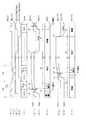
ここで図17は、この特開2007−133284号公報に開示の表示装置を示す接続図である。この表示装置1は、水平セレクタ(HSEL)2により信号線駆動回路3が構成され、またライトスキャナ(WSCN)4A、ドライブスキャナ(DSCN)4Bにより走査線駆動回路5が構成される。 Here, FIG. 17 is a connection diagram showing a display device disclosed in Japanese Patent Laid-Open No. 2007-133284. In the
ここで水平セレクタ2は、表示部6の信号線SIGにそれぞれ対応する複数のラッチ回路で入力画像データD1を順次ラッチすることにより、この画像データD1を各信号線SIGに振り分ける。また各信号線SIGに振り分けた画像データD1をそれぞれディジタルアナログ変換処理し、各信号線SIGに接続された各画素の階調を順次示す駆動信号Ssigを信号線SIG毎に生成する。水平セレクタ2は、この駆動信号Ssigを対応する信号線SIGに出力する。 Here, the
ライトスキャナ4A、ドライブスキャナ4Bは、それぞれ図示しない信号生成回路で生成された基準信号を順次転送することにより、各走査線の駆動信号DS、WSを生成し、この駆動信号DS、WSをそれぞれ対応する走査線に出力する。 The
表示部6は、所定の画素回路7をマトリックス状に配置して形成される。ここで画素回路7は、信号レベル保持用コンデンサC1の両端をそれぞれゲート及びソースに接続したソースフォロワ回路構成のNMOSトランジスタTR1(以下、駆動トランジスタと呼ぶ)により、電流駆動型の発光素子である有機EL素子8を駆動する。なおここでCpは、有機EL素子8の容量成分である。またVss1は、有機EL素子8のカソード電圧である。 The
この駆動トランジスタTR1は、ドライブスキャナ4Bから出力される駆動信号DSによりオンオフ動作するNMOSトランジスタTR2を介して、駆動用電源Vddにドレインが接続される。これにより画素回路7は、駆動信号DSによるトランジスタTR2のオンオフ制御により駆動トランジスタTR1への電源Vddの供給が制御され、有機EL素子8の発光、非発光が制御される。 The drain of the driving transistor TR1 is connected to the driving power supply Vdd via the NMOS transistor TR2 that is turned on / off by the driving signal DS output from the
また駆動トランジスタTR1は、ライトスキャナ4Aから出力される駆動信号である書込み信号WSによりオンオフ動作するNMOSトランジスタTR5を介して、ゲートが信号線SIGに接続される。これにより画素回路7は、信号線SIGを介して駆動トランジスタTR1のゲートに接続された信号レベル保持用コンデンサC1の一端の電圧を所望の電圧に設定できるように構成される。 Further, the gate of the driving transistor TR1 is connected to the signal line SIG via the NMOS transistor TR5 that is turned on / off by a write signal WS that is a driving signal output from the
ここで画素回路7は、トランジスタTR2により駆動トランジスタTR1の電源の供給が停止されて有機EL素子8の発光を停止する非発光期間が開始し、トランジスタTR5のオン動作により、信号線SIGを介して信号レベル保持用コンデンサC1のゲート側端の電圧が一旦立ち上げられる。この場合、信号レベル保持用コンデンサC1の有機EL素子8側端の電圧は、ゲート側端の電圧の上昇により一旦上昇するものの、有機EL素子8による放電により、有機EL素子8のしきい値電圧に保持される。 Here, the pixel circuit 7 starts a non-light emission period in which the transistor TR2 stops supplying power to the drive transistor TR1 and stops the light emission of the
続いて画素回路7は、信号線SIGを介して信号レベル保持用コンデンサC1のゲート側端の電圧が立ち下げられ、これと連動して信号レベル保持用コンデンサC1によるカップリングにより信号レベル保持用コンデンサC1の有機EL素子8側端が有機EL素子8のしきい値電圧以下の電圧に立ち下がる。この信号線SIGの電圧の立ち上げ及び立ち下げにより画素回路7は、信号レベル保持用コンデンサC1の端子間電圧が駆動トランジスタTR1のしきい値電圧Vth以上の電圧に設定され、しきい値電圧Vthのばらつきを補正する前の準備段階の処理が完了する。 Subsequently, in the pixel circuit 7, the voltage at the gate side end of the signal level holding capacitor C1 is lowered via the signal line SIG, and in conjunction with this, the signal level holding capacitor C1 is coupled by coupling with the signal level holding capacitor C1. The end of the C1 side of the
続いて画素回路7は、トランジスタTR2により駆動トランジスタTR1への電源の供給が開始され、これにより信号レベル保持用コンデンサC1の端子間電圧によるゲートソース間電圧により駆動トランジスタTR1によって信号レベル保持用コンデンサC1の有機EL素子8側端が徐々に充電され、信号レベル保持用コンデンサC1の端子間電圧が徐々に低下する。またこの信号レベル保持用コンデンサC1の端子間電圧が駆動トランジスタTR1のしきい値電圧Vthにまで低下すると、駆動トランジスタTR1による充電の処理が停止する。これにより画素回路7は、信号レベル保持用コンデンサC1の端子間電圧が駆動トランジスタTR1のしきい値電圧Vthに設定される。これにより画素回路7は、駆動トランジスタTR1のしきい値電圧Vthのばらつき補正処理が完了する。 Subsequently, in the pixel circuit 7, the supply of power to the drive transistor TR1 is started by the transistor TR2, and thereby the signal level holding capacitor C1 is driven by the drive transistor TR1 by the gate-source voltage due to the voltage between the terminals of the signal level holding capacitor C1. The side end of the
画素回路7では、この駆動トランジスタTR1によって信号レベル保持用コンデンサC1の有機EL素子8側端を充電して、信号レベル保持用コンデンサC1の端子間電圧を駆動トランジスタTR1のしきい値電圧Vthに設定する期間が、所定の休止期間を間に挟んで複数回の期間に設定される。なお1水平走査期間で十分な期間を確保できる場合には、1水平走査期間で準備処理からの一連の処理を実行するようにしてもよい。 In the pixel circuit 7, the driving transistor TR1 charges the end of the signal level holding capacitor C1 on the
続いて画素回路7は、トランジスタTR5を介してトランジスタTR1のゲートに有機EL素子8の発光輝度を指示する階調電圧が設定され、これにより信号レベル保持用コンデンサC1に設定された駆動トランジスタTR1のしきい値電圧Vthにより階調電圧が補正されて信号レベル保持用コンデンサC1の端子間電圧が設定される。 Subsequently, in the pixel circuit 7, a gradation voltage that indicates the light emission luminance of the
画素回路7は、トランジスタTR5により信号線SIGを駆動トランジスタTR1のゲートに接続した状態で、一定期間の間、トランジスタTR2により駆動トランジスタTR1に電源が供給された後、トランジスタTR5がオフ状態に設定されて発光期間が開始する。 In the pixel circuit 7, in the state where the signal line SIG is connected to the gate of the driving transistor TR1 by the transistor TR5, power is supplied to the driving transistor TR1 by the transistor TR2 for a certain period, and then the transistor TR5 is set to an off state. The light emission period starts.
この特開2007−133284号公報に開示の構成によれば、休止期間を間に挟んでしきい値電圧のばらつきを補正する処理を複数回の期間で実行することにより、高解像度化により1水平走査期間の間でしきい値電圧のばらつき補正処理に十分な期間を確保できない場合でも、複数の水平走査期間で十分な時間を確保してしきい値電圧Vthのばらつき補正処理を実行することができる。 According to the configuration disclosed in Japanese Patent Application Laid-Open No. 2007-133284, a process for correcting a variation in threshold voltage with a pause period in between is executed in a plurality of periods, thereby increasing the resolution to one horizontal level. Even when it is not possible to secure a sufficient period for the variation correction process of the threshold voltage during the scanning period, it is possible to execute the variation correction process of the threshold voltage Vth while ensuring a sufficient time in a plurality of horizontal scanning periods. it can.
またトランジスタTR5により信号線SIGを駆動トランジスタTR1のゲートに接続した状態で、一定期間の間、トランジスタTR2により駆動トランジスタTR1に電源を供給した後、トランジスタTR5をオフ状態に設定することにより、駆動トランジスタTR1の移動度が大きい画素回路7程、信号レベル保持用コンデンサC1の端子間電圧を低減することができ、これにより駆動トランジスタTR1の移動度のばらつきによる発光輝度のばらつきを防止することができる。 Further, the transistor TR5 is connected to the gate of the driving transistor TR1 and the power supply is supplied to the driving transistor TR1 by the transistor TR2 for a certain period, and then the transistor TR5 is set to the off state. The pixel circuit 7 having a higher mobility of TR1 can reduce the voltage across the terminals of the signal level holding capacitor C1, thereby preventing variations in light emission luminance due to variations in mobility of the drive transistor TR1.
ところこの図17の構成では、1つの画素回路7に3つのトランジスタを設けることが必要であり、画素回路7の構成が複雑な欠点がある。この欠点を解消する1つの方法として、電源制御用のトランジスタTR2を省略して走査線駆動回路により駆動トランジスタTR1の電源を制御する方法が考えられる。 However, in the configuration of FIG. 17, it is necessary to provide three transistors in one pixel circuit 7, and there is a disadvantage that the configuration of the pixel circuit 7 is complicated. As one method for solving this drawback, a method in which the power supply control transistor TR2 is omitted and the power supply of the drive transistor TR1 is controlled by the scanning line drive circuit is conceivable.
図18は、このトランジスタTR2を省略して考えられる表示装置を示す接続図である。この図18において、図17と同一の構成は、対応する符号を付して示し、重複した説明は省略する。この表示装置11は、所定の絶縁基板上に表示部12が作成され、この表示部12の周囲に信号線駆動回路13及び走査線駆動回路14が設けられる。信号線駆動回路13には、水平セレクタ(HSEL)15が設けられ、また走査線駆動回路14には、ライトスキャナ(WSCN)16A、ドライブスキャナ(DSCN)16Bが設けられる。 FIG. 18 is a connection diagram showing a display device that can be considered by omitting the transistor TR2. In FIG. 18, the same components as those in FIG. 17 are denoted by the corresponding reference numerals, and redundant description is omitted. In the
水平セレクタ15は、水平セレクタ2と同様にして各信号線SIGに画像データD1を振り分けてディジタルアナログ変換処理する。水平セレクタ15は、所定の固定電圧Vofsとこのディジタルアナログ変換結果とを交互に出力することにより、固定電圧Vofsを間に挟んで、信号線SIGに接続された各画素の階調を示す階調電圧Vsigの連続による駆動信号Ssigを各信号線SIGに出力する(図19(C)参照)。 The
ライトスキャナ16A、ドライブスキャナ16Bは、それぞれ図示しない信号生成回路で生成された基準信号を順次転送することにより、各走査線の駆動信号DS、WSを生成し、この駆動信号DS、WSをそれぞれ対応する走査線に出力する。 The
表示部12は、画素回路17をマトリックス状に配置して作成される。ここで画素回路17は、駆動トランジスタTR1の電源を制御するトランジスタTR2が省略された点、このトランジスタTR2の省略に関連する構成が異なる点を除いて、図17の画素回路7と同一に構成される。 The
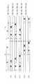
ここで図19は、この画素回路17の動作の説明に供するタイムチャートである。なお以下においては、説明の簡略化のため、信号レベル保持用コンデンサC1の容量に対して駆動トランジスタTR1のゲートノードの寄生容量は十分に小さいと仮定し、有機EL素子8の容量Cpは信号レベル保持用コンデンサC1の容量に比して十分に大きいと仮定する。またこの表示装置11は、フィールド単位のライン順次により各画素回路17の発光輝度を設定し、これに対応して図19では、連続するラインに関する信号、構成を符号i、i+1を用いて示す。また信号レベル保持用コンデンサC1の端子間電圧を駆動トランジスタTR1のしきい値電圧Vth以上に設定する準備処理の期間を「準備」により示す。またこの駆動トランジスタTR1のしきい値電圧Vth以上に設定された信号レベル保持用コンデンサC1の端子間電圧を1回の期間で駆動トランジスタTR1のしきい値電圧Vthに設定するものとして、この期間を「Vth補正」により示し、その後、駆動トランジスタTR1の移動度のばらつきを補正する期間を「μ補正」により示す。 Here, FIG. 19 is a time chart for explaining the operation of the
図19に示すように、各画素回路17は、有機EL素子8の発光を停止させる非発光期間T1が時点t1で開始すると、駆動信号DSの電圧が発光期間T2の電圧Vddから基準電圧Vss2に立ち下げられる(図19(B1)及び(B2))。ここでこの基準電圧Vss2は、有機EL素子8のカソード電圧Vss1に有機EL素子8のしきい値電圧を加算した電圧より低い電圧に設定される。これにより画素回路17は、駆動トランジスタTR1の駆動信号DS側端がソースとして機能し、有機EL素子8のアノード電圧が立ち下がり、有機EL素子8が発光を停止する。また駆動トランジスタTR1を介して信号レベル保持用コンデンサC1の有機EL素子8側端から蓄積電荷が放電し、これにより信号レベル保持用コンデンサC1の有機EL素子8側端の電圧(駆動トランジスタTR1のソース電圧Vs)(図19(E1)及び(E2))が電圧Vss2に設定される。 As shown in FIG. 19, in each
また画素回路17は、駆動信号Ssigにより信号線SIGが所定電圧Vofsに立ち下げられると、書込み信号WSにより書込トランジスタTR5がオン状態に切り換えられる(図19(A1)、(A2)及び(C))。これにより画素回路17は、駆動トランジスタTR1のゲート電圧Vg(図19(D1)及び(D2))がこの信号線SIGの電圧Vofsに設定され、信号レベル保持用コンデンサC1の端子間電圧がVofs−Vss2に設定される。ここで画素回路17では、この端子間電圧Vofs−Vss2が駆動トランジスタTR1のしきい値電圧をVthより大きくなるように(Vss2<Vofs−Vth)、電圧Vofs、Vss2が設定される。 Further, in the
これにより画素回路17では、信号レベル保持用コンデンサC1の端子間電圧が駆動トランジスタTR1のしきい値電圧Vthより大きな電圧に設定され、信号レベル保持用コンデンサC1に駆動トランジスタTR1のしきい値電圧Vthを設定するための準備処理が実行される(図19(F1)及び(F2))。なおこれにより基準電圧Vofsは、駆動トランジスタTR1のしきい値電圧Vthのばらつき補正後に駆動トランジスタTR1がオン動作しない電圧である必要がある。すなわち有機EL素子8のしきい値電圧をVtholedとすると、Vofs<Vss1+Vtholed+Vthを満たす必要がある。 Thereby, in the
続いて画素回路17は、駆動信号Ssigが固定電位Vofsに保持されている期間の時点t2で、書込トランジスタTR5をオン状態に保持したままの状態で、駆動信号DSが発光期間T2の電圧Vddに立ち上げられて駆動トランジスタTR1への電源の供給が開始される(図19(B1)及び(B2))。また続いて信号線SIGの信号レベルが階調電圧Vsigに設定される直前の時点で、書込み信号WSにより書込トランジスタTR5がオフ状態に切り換えられる。 Subsequently, the
これにより画素回路17は、信号レベル保持用コンデンサC1の端子間電圧が駆動トランジスタTR1のしきい値電圧Vthより大きい場合であることを条件に、駆動トランジスタTR1を介して電源Vddにより信号レベル保持用コンデンサC1の有機EL素子8側端に充電電流が流れ、駆動トランジスタTR1のソース電圧Vsが徐々に上昇する(図19(D1)、(D2)、(E1)及び(E2))。その結果、画素回路17は、信号レベル保持用コンデンサC1の端子間電圧が徐々に駆動トランジスタTR1のしきい値電圧Vthに接近する。また信号レベル保持用コンデンサC1の端子間電圧が駆動トランジスタTR1のしきい値電圧Vthとなると、ソース電圧Vsの上昇が停止する。これにより画素回路17は、信号レベル保持用コンデンサC1の端子間電圧が駆動トランジスタTR1のしきい値電圧Vthに設定される。 As a result, the
画素回路17は、続いて駆動信号Ssigが当該画素回路17の階調電圧Vsigに設定されている時点t3で書込み信号WSが立ち上げられて書込トランジスタTR5がオン状態に設定され(図19(A1)及び(A2))、これにより駆動トランジスタTR1のゲートが信号線SIGに接続される。また一定期間Tμが経過した時点で、書込み信号WSが立ち下げられ、これにより信号線SIGに出力されている駆動信号Ssigの階調電圧Vsigが信号レベル保持用コンデンサC1の一端にホールドされる。これにより画素回路17は、信号レベル保持用コンデンサC1に設定された駆動トランジスタTR1のしきい値電圧Vthにより補正して、信号レベル保持用コンデンサC1の端子間電圧が階調電圧Vsigに応じた電圧に設定される。これによりこの表示装置11では、駆動トランジスタTR1のしきい値電圧Vthのばらつきによる画質劣化を防止することができる。 In the
ここでこの期間Tμにおいては、駆動トランジスタTR1のゲートを信号線SIGに接続した状態で駆動トランジスタTR1に電源Vddを供給していることから、駆動トランジスタTR1は、ゲートソース間電圧Vgsに応じてソース電圧Vsが徐々に上昇することになる。またここでこのソース電圧Vsの上昇速度は、(1)式により駆動トランジスタTR1の移動度が大きい場合程、早くなる。またソース電圧Vsが上昇すると、ゲートソース間電圧Vgsが低下することにより、ソース電流が流れ難くなる。 In this period Tμ, since the power supply Vdd is supplied to the drive transistor TR1 with the gate of the drive transistor TR1 connected to the signal line SIG, the drive transistor TR1 has a source corresponding to the gate-source voltage Vgs. The voltage Vs gradually increases. Here, the rising speed of the source voltage Vs is faster as the mobility of the driving transistor TR1 is larger according to the equation (1). Further, when the source voltage Vs increases, the gate-source voltage Vgs decreases, so that the source current hardly flows.
これにより画素回路17は、この一定期間Tμにより、移動度が大きい駆動トランジスタ程、信号レベル保持用コンデンサC1の端子間電圧が低下し、移動度のばらつきを補正して画質の劣化が防止される。なおこの期間Tμにおける、駆動トランジスタTR1のドレイン電流は、次式により表される。 As a result, the
画素回路17は、時点t4で書込み信号WSが立ち下げられると、発光期間T2が開始し、信号レベル保持用コンデンサC1の端子間電圧によるゲートソース間電圧Vgsにより有機EL素子8を電流駆動する。なおこの発光期間T2において、画素回路17は、有機EL素子8の容量Cpによる駆動トランジスタTR1のブートストラップ動作により、期間Tμで設定された駆動トランジスタTR1のゲート電圧Vg及びソース電圧Vsが徐々に上昇して有機EL素子8が発光を開始し、やがてこれらゲート電圧Vg及びソース電圧Vsの上昇が停止してこれらゲート電圧Vg及びソース電圧Vsが一定電圧に保持される。なおこの発光期間T2では、駆動トランジスタTR1が飽和動作するように電源電圧Vdd2(Vdd2>Vtholed+Vgs−Vth)を設定する必要がある。 When the write signal WS falls at time t4, the
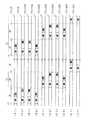
これによりこの図18の例では、図20により示すように、1水平走査毎のライン順次により連続するラインi、i+1、i+2、i+3、……の画素回路17(i)、17(i+1)、17(i+2)、17(i+3)、……の階調を設定して、所望の画像を表示する。なおここでこの図20では、しきい値電圧の補正処理を「補」により示し、信号レベル保持用コンデンサC1への信号線SIGの電圧Vsigの設定を「書」により示す。 Accordingly, in the example of FIG. 18, as shown in FIG. 20, the pixel circuits 17 (i), 17 (i + 1) of the lines i, i + 1, i + 2, i + 3,. The gradations of 17 (i + 2), 17 (i + 3),... Are set and a desired image is displayed. In FIG. 20, the threshold voltage correction processing is indicated by “complement”, and the setting of the voltage Vsig of the signal line SIG to the signal level holding capacitor C1 is indicated by “letter”.
このような画素回路の構成に関して、特表2002−514320号公報、特開2004−133240号公報、特開2004−246204号公報には、信号レベル保持用コンデンサに設定された駆動トランジスタのしきい値電圧に依存した電圧により階調電圧を補正して駆動トランジスタに設定することにより、駆動トランジスタのしきい値電圧のばらつきを補正する方法が提案されている。また特開2005−345722号公報、特開2006−215213号公報、特開2007−133282号公報には、同様に駆動トランジスタのしきい値電圧のばらつきを補正する方法が提案されている。 Regarding the configuration of such a pixel circuit, Japanese Unexamined Patent Publication No. 2002-514320, Japanese Patent Application Laid-Open No. 2004-133240, and Japanese Patent Application Laid-Open No. 2004-246204 disclose a threshold value of a driving transistor set as a signal level holding capacitor. There has been proposed a method of correcting a variation in threshold voltage of a driving transistor by correcting a gradation voltage with a voltage depending on the voltage and setting the driving voltage in the driving transistor. Similarly, Japanese Patent Laid-Open Nos. 2005-345722, 2006-215213, and 2007-133282 propose methods for correcting variations in threshold voltages of drive transistors.
しかしながらこの図20に示すように、1水平走査毎のライン順次により連続するラインi、i+1、i+2、i+3、……の画素回路17(i)、17(i+1)、17(i+2)、17(i+3)、……の階調を設定する場合、高解像度化により1水平走査期間が短くなると、しきい値電圧Vthのばらつき補正に十分な時間を確保できなくなる恐れがある。 However, as shown in FIG. 20, the pixel circuits 17 (i), 17 (i + 1), 17 (i + 2), 17 (17) of the lines i, i + 1, i + 2, i + 3,. When the gradation of i + 3),... is set, if one horizontal scanning period is shortened due to higher resolution, there is a possibility that sufficient time cannot be secured for correcting the variation of the threshold voltage Vth.
この問題を解決する1つの方法として、図20との対比により図21に示すように、連続する複数ラインで同時にしきい値電圧Vthのばらつき補正処理を実行した後、ライン順次で各画素回路の階調を設定する方法が考えられる。すなわちこの場合、図19との対比により図22に示すように、基準電圧Vofs、先頭ライン側の画素の階調を示す階調電圧Vsig(i)、続くラインの画素の階調を示す階調電圧Vsig(i+1)が順次連続するように各信号線SIGに駆動信号Ssigを出力し、信号線SIGの電圧が基準電圧Vofsに設定されている期間で、この連続する2つのラインi、i+1でしきい値電圧Vthのばらつき補正処理を実行する。またそれぞれ信号線SIGの電圧が階調電圧Vsig(i)及びVsig(i+1)に設定されている期間で、各ラインi、i+1の階調を設定する。 As one method for solving this problem, as shown in FIG. 21 in comparison with FIG. 20, after performing the variation correction processing of the threshold voltage Vth simultaneously on a plurality of continuous lines, each pixel circuit is sequentially processed in the line order. A method of setting the gradation can be considered. That is, in this case, as shown in FIG. 22 in comparison with FIG. 19, the reference voltage Vofs, the gradation voltage Vsig (i) indicating the gradation of the pixel on the head line side, and the gradation indicating the gradation of the pixel of the subsequent line The drive signal Ssig is output to each signal line SIG so that the voltage Vsig (i + 1) is successively continued, and in the period when the voltage of the signal line SIG is set to the reference voltage Vofs, A variation correction process of the threshold voltage Vth is executed. In addition, the gray levels of the lines i and i + 1 are set in a period in which the voltage of the signal line SIG is set to the gray voltages Vsig (i) and Vsig (i + 1), respectively.
しかしながらこのようにして複数ラインで同時にしきい値電圧Vthのばらつき補正処理を実行する場合、これらのライン間で、微妙に発光輝度が相違し、その結果、横方向にすじが発生して画質が劣化することが判った。
本発明は以上の点を考慮してなされたもので、複数ラインで同時に駆動トランジスタのしきい値電圧のばらつき補正処理を実行する場合に、横方向のすじの発生を防止して画質の劣化を有効に回避することができる画像表示装置及び画像表示方法を提案しようとするものである。 The present invention has been made in consideration of the above points, and when performing variation correction processing of threshold voltages of driving transistors simultaneously on a plurality of lines, the occurrence of horizontal streaks is prevented and image quality deterioration is prevented. The present invention intends to propose an image display apparatus and an image display method that can be effectively avoided.
上記の課題を解決するため請求項1の発明は、画素回路をマトリックス状に配置して形成された表示部に対して、信号線駆動回路及び走査線駆動回路により前記画素回路を駆動することにより、前記表示部で所望の画像を表示する画像表示装置に適用して、前記画素回路は、少なくとも発光素子と、信号レベル保持用コンデンサと、前記発光素子を駆動する駆動トランジスタと、前記走査線駆動回路から出力される書込み信号によりオン動作する書込トランジスタとを有し、前記信号線駆動回路及び走査線駆動回路の駆動により、非発光期間と発光期間とを繰り返し、前記非発光期間において、前記信号レベル保持用コンデンサの端子間電圧を前記駆動トランジスタのしきい値電圧に依存した電圧に設定するしきい値電圧のばらつき補正処理を実行した後、前記書込トランジスタをオン動作させて、前記発光素子の発光輝度を示す階調電圧を前記信号レベル保持用コンデンサに設定された電圧で補正して前記駆動トランジスタに設定する階調設定処理を実行し、前記発光期間において、前記駆動トランジスタにより前記発光素子を駆動して前記階調設定処理で設定された階調で前記発光素子を発光させ、前記表示部は、前記信号線駆動回路及び走査線駆動回路の駆動により、複数ラインの前記画素回路において、前記しきい値電圧のばらつき補正処理を同時に実行した後、前記階調設定処理を順次実行し、前記複数ラインの前記画素回路において、時間軸方向及び又は走査線方向に、前記しきい値電圧のばらつき補正処理に対する前記階調設定処理の順序を入れ換える。 In order to solve the above problems, the invention of
また請求項10の発明は、画素回路をマトリックス状に配置して形成された表示部に対して、信号線駆動回路及び走査線駆動回路により前記画素回路を駆動することにより、前記表示部で所望の画像を表示する画像表示装置における画像表示方法に適用して、前記画素回路は、少なくとも発光素子と、信号レベル保持用コンデンサと、前記発光素子を駆動する駆動トランジスタと、前記走査線駆動回路から出力される書込み信号によりオン動作する書込トランジスタとを有し、前記画像表示方法は、前記信号線駆動回路及び走査線駆動回路の駆動により、前記発光素子の発光を停止させる非発光ステップと、前記発光素子を発光させる発光ステップとを繰り返し、前記非発光ステップにおいて、前記信号レベル保持用コンデンサの端子間電圧を前記駆動トランジスタのしきい値電圧に依存した電圧に設定するしきい値電圧のばらつき補正処理を実行した後、前記書込トランジスタをオン動作させて、前記発光素子の発光輝度を示す階調電圧を前記信号レベル保持用コンデンサに設定された電圧で補正して前記駆動トランジスタに設定する階調設定処理を実行し、前記発光ステップにおいて、前記駆動トランジスタにより前記発光素子を駆動して前記階調設定処理で設定された階調で前記発光素子を発光させ、前記非発光ステップにおいて、前記信号線駆動回路及び走査線駆動回路の駆動により、複数ラインの前記画素回路において、前記しきい値電圧のばらつき補正処理を同時に実行した後、前記階調設定処理を順次実行し、前記複数ラインの前記画素回路において、時間軸方向及び又は走査線方向に、前記しきい値電圧のばらつき補正処理に対する前記階調設定処理の順序を入れ換える。 According to a tenth aspect of the present invention, in the display unit formed by arranging pixel circuits in a matrix, the pixel unit is driven by a signal line driving circuit and a scanning line driving circuit, so that the display unit has a desired configuration. The pixel circuit includes at least a light emitting element, a signal level holding capacitor, a driving transistor for driving the light emitting element, and the scanning line driving circuit. A non-light emitting step of stopping light emission of the light emitting element by driving the signal line driving circuit and the scanning line driving circuit, and a writing transistor that is turned on by an output writing signal. A light emission step of causing the light emitting element to emit light, and in the non-light emission step, the voltage across the terminals of the signal level holding capacitor After executing threshold voltage variation correction processing that is set to a voltage that depends on the threshold voltage of the driving transistor, the write transistor is turned on to generate a gradation voltage that indicates the light emission luminance of the light emitting element. A gradation setting process for correcting the voltage set in the signal level holding capacitor and setting the driving transistor is executed, and in the light emission step, the light emitting element is driven by the driving transistor to perform the gradation setting process. The light emitting element is caused to emit light at a gradation set in step (b), and in the non-light emission step, the threshold voltage variations are corrected in the pixel circuits of a plurality of lines by driving the signal line driving circuit and the scanning line driving circuit. After simultaneously executing the processing, the gradation setting processing is sequentially executed, and in the pixel circuits of the plurality of lines, the time axis direction and Or the scanning line direction, replacing the order of the gradation setting process for variation correction processing of the threshold voltage.
請求項1又は請求項10の構成によれば、同時にしきい値電圧のばらつき補正処理を実行する複数ライン間における微妙な発光輝度の相違を目立たなくすることができ、その結果、横方向のすじの発生を防止して画質の劣化を有効に回避することができる。 According to the configuration of
本発明によれば、複数ラインで同時に駆動トランジスタのしきい値電圧のばらつき補正処理を実行する場合に、横方向のすじの発生を防止して画質の劣化を有効に回避することができる。 According to the present invention, when the variation correction process of threshold voltages of the drive transistors is simultaneously performed on a plurality of lines, it is possible to effectively prevent the deterioration of the image quality by preventing the occurrence of horizontal stripes.
以下、適宜図面を参照しながら本発明の実施例を詳述する。 Hereinafter, embodiments of the present invention will be described in detail with reference to the drawings as appropriate.
(1)実施例1の構成
図2は、本発明の実施例1の表示装置を示すブロック図である。この表示装置21は、所定の絶縁基板上に表示部22が作成され、この表示部22の周囲に信号線駆動回路23及び走査線駆動回路24が設けられる。ここで表示部22は、赤色、緑色、青色の画素をそれぞれ構成する赤色、緑色、青色の画素回路(PIX)17R、17G、17Bがマトリックス状に配置して形成される。なおこれら赤色、緑色、青色の画素回路17R、17G、17Bは、出射光の波長が異なる点を除いて、図18の画素回路17と同一に構成される。なお図2との対比により図3に示すように、赤色、緑色、青色の画素回路17R、17G、17Bに代えて、単色の画素回路17を順次マトリックス状に配置して表示部22Aを構成する場合等にも、広く適用することができる。(1) Configuration of
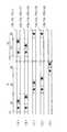
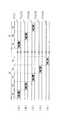
この実施例において、表示部22は、図21との対比により図1に示すように、連続する複数ラインで同時にしきい値電圧Vthのばらつき補正処理を実行する。また続いて、順次、この複数ラインにおいて各画素回路の階調を設定するようにし、複数ラインにおける階調の設定順序を時間軸方向に入れ換える。 In this embodiment, as shown in FIG. 1 in comparison with FIG. 21, the
より具体的にこの実施例では、この連続する複数ラインが2ラインに設定され、この2ラインにおける階調の設定順序が偶数フィールドと奇数フィールドとで入れ代わるようにし、これによりこの2ラインにおける階調の設定順序が時間軸方向に入れ代わるようにする。すなわちフィールド毎に、画素回路17R(i)、17G(i)、17B(i)及び17R(i+1)、17G(i+1)、17B(i+1)による2つのラインの画素回路で同時にしきい値電圧Vthのばらつき補正処理を実行する。また奇数フィールドでは、これら画素回路17R(i)、17G(i)、17B(i)及び17R(i+1)、17G(i+1)、17B(i+1)のうちの、先頭ライン側の画素回路17R(i)、17G(i)、17B(i)で階調設定処理を実行した後、続いて続くラインの画素回路17R(i+1)、17G(i+1)、17B(i+1)で階調設定処理を実行する。また偶数フィールドでは、これとは逆に、画素回路17R(i+1)、17G(i+1)、17B(i+1)で階調設定処理を実行した後、先頭ライン側の画素回路17R(i)、17G(i)、17B(i)で始めに階調設定処理を実行する。 More specifically, in this embodiment, the continuous plural lines are set to two lines, and the setting order of gradations in the two lines is switched between the even field and the odd field, whereby the gradations in the two lines are changed. The order of setting is changed in the time axis direction. That is, for each field, the threshold voltage Vth is simultaneously applied to the pixel circuits of two lines of the
これに対応して図4に示すように、信号線駆動回路23は、図示しない水平セレクタにより各信号線SIGに画像データD1を振り分けて一時保持し、この画素回路への階調設定順序に対応する順序でアナログディジタル変換処理する。また基準電圧Vofsを間に挟んで、奇数フィールドでは、アナログディジタル変換結果である階調電圧Vsig(i)、Vsig(i+1)、……を順次出力し、偶数フィールドでは階調電圧Vsig(i+1)、Vsig(i)を順次出力する。 Corresponding to this, as shown in FIG. 4, the signal
またこれに対応して走査線駆動回路24は、ドライブスキャナ(DSCN)24A及びライトスキャナ(WSCN)24Bより駆動信号DS及び書込信号WSをフィールド毎に切り換えて出力する。またこの連続する2ラインにおける階調設定処理の時間的なずれTに対応するように、駆動信号DSを立ち下げるタイミングを切り換え(図4(B1)及び(B2))、これらの2ラインにおける発光期間を等しい時間に設定する。 Corresponding to this, the scanning
(2)実施例の動作
以上の構成において、この表示装置21では(図1)、信号線駆動回路23及び走査線駆動回路24による表示部22の駆動により順次表示部22の画素回路17R、17G、17Bに信号線SIGの階調電圧Vsigが設定されると共に、この設定された階調電圧Vsigにより各画素回路17R、17G、17Bの有機EL素子8が発光し、所望の画像が表示部22で表示される。(2) Operation of Example In the above configuration, in the display device 21 (FIG. 1), the
すなわちこの表示装置21では、非発光期間T1において(図4)、各画素回路17R、17G、17Bに設けられた信号レベル保持用コンデンサC1の一端が信号線SIGの階調電圧Vsigに設定され、この信号レベル保持用コンデンサC1の端子間電圧によるゲートソース間電圧Vgsにより駆動トランジスタTR1で有機EL素子8が駆動される。これによりこの表示装置では、信号線SIGの階調電圧Vsigに応じた発光輝度で各画素回路17R、17G、17Bの有機EL素子8が発光する。 That is, in the
表示装置21は、この階調電圧Vsigの設定に先立って、始めに信号レベル保持用コンデンサC1の両端電圧差が駆動トランジスタTR1のしきい値電圧Vth以上の電圧に設定され、これにより駆動トランジスタTR1のしきい値電圧Vthのばらつき補正の準備処理が実行される。その後、表示装置21は、この信号レベル保持用コンデンサC1の端子間電圧に応じた電流により信号レベル保持用コンデンサC1のソース側端が充電され、信号レベル保持用コンデンサC1の端子間電圧が駆動トランジスタTR1のしきい値電圧に設定される。これにより表示装置21は、信号レベル保持用コンデンサC1に駆動トランジスタTR1のしきい値電圧Vthがセットされ、駆動トランジスタTR1のしきい値電圧Vthのばらつき補正処理が実行される。 Prior to the setting of the gradation voltage Vsig, the
表示装置21は、その後、駆動トランジスタTR1のゲートが信号線SIGに接続されて信号レベル保持用コンデンサC1の一端の電圧が階調電圧Vsigに設定されることにより、駆動トランジスタTR1のしきい値電圧Vthにより補正して信号レベル保持用コンデンサC1の端子間電圧が階調電圧Vsigに対応する電圧に設定される。これにより表示装置21では、駆動トランジスタTR1のしきい値電圧のばらつきによる画質劣化が有効に回避される。 Thereafter, the
また階調電圧Vsigを設定する際の一定期間Tμの間、信号線SIGに接続されて駆動トランジスタTR1に電源が供給され、これにより信号レベル保持用コンデンサC1の端子間電圧が駆動トランジスタTR1の移動度により補正されて、駆動トランジスタTR1の移動度のばらつきによる画質劣化が防止される。 Further, for a certain period Tμ when setting the gradation voltage Vsig, the power is supplied to the driving transistor TR1 connected to the signal line SIG, whereby the voltage between the terminals of the signal level holding capacitor C1 moves the driving transistor TR1. The image quality is prevented from being deteriorated due to variations in mobility of the drive transistor TR1.
表示装置21では、これらの駆動トランジスタTR1のしきい値電圧Vthのばらつき補正処理が、連続する複数ラインで同時に実行された後、この複数ラインで順次各画素回路の階調が設定され、これにより高解像度化によりライン数が増大して1水平走査期間が短くなった場合でも、駆動トランジスタTR1のしきい値電圧Vthのばらつき補正に十分な時間を確保することができ、しきい値電圧Vthのばらつきによる発光輝度のばらつきを補正して高画質により画像表示することができる。 In the
しかしながらこのように連続する複数ラインで駆動トランジスタTR1のしきい値電圧Vthのばらつき補正処理を同時に実行した後、単に、各ラインの階調を順次設定したのでは、これらの複数のライン間で、微妙に発光輝度が相違し、その結果、横方向にすじが発生して画質が劣化することになる。 However, after simultaneously executing the variation correction processing of the threshold voltage Vth of the drive transistor TR1 in a plurality of continuous lines in this way, simply setting the gradation of each line sequentially, The emission brightness is slightly different, and as a result, horizontal stripes are generated and the image quality is deteriorated.
そこでこの表示装置21では、駆動トランジスタTR1のしきい値電圧Vthのばらつき補正処理を同時に実行する複数ラインにおいて、時間軸方向に、階調設定の順序が入れ換えられる(図1)。その結果、これらの複数のラインの画素回路では、しきい値電圧のばらつき補正処理を実行した後、階調設定までの平均時間が等しくなり、その結果、これらの複数ライン間における微妙な発光輝度の相違を目立たなくすることができ、横方向のすじの発生を防止して画質の劣化を有効に回避することができる。 Therefore, in this
より具体的に、この表示装置21では、連続する2ラインで同時に駆動トランジスタTR1のしきい値電圧Vthのばらつき補正処理を実行するようにして、この2ラインにおける階調設定の順序をフィールド毎に入れ換えて時間軸方向に階調設定の順序が入れ換えられ、これにより横方向のすじの発生を防止して画質の劣化を有効に回避することができる。 More specifically, in this
またこの入れ換えにより変化する発光期間の開始時点に対応するように、発光期間の終了時点を切り換えて各ラインで発光期間が等しくなるように設定し、これによっても一段と複数のライン間における微妙な発光輝度の相違を目立たなくして画質を向上することができる。 In addition, the end point of the light emission period is switched so as to correspond to the start point of the light emission period that changes due to this replacement, and the light emission period is set to be equal for each line, which also makes subtle light emission between a plurality of lines even more. The image quality can be improved without making the difference in brightness inconspicuous.
(3)実施例の効果
以上の構成によれば、駆動トランジスタのしきい値電圧のばらつき補正処理を複数ラインで同時に実行するようにして、この複数ラインにおいて、時間軸方向に、階調設定の順序を入れ換えることにより、これらの複数のライン間における微妙な発光輝度の相違を目立たなくすることができ、横方向のすじの発生を防止して画質の劣化を有効に回避することができる。(3) Advantages of Embodiment According to the above configuration, the threshold voltage variation correction processing of the drive transistor is performed simultaneously on a plurality of lines, and the gradation setting is performed in the time axis direction on the plurality of lines. By changing the order, it is possible to make a subtle difference in light emission luminance between the plurality of lines inconspicuous, and it is possible to effectively prevent deterioration of image quality by preventing occurrence of horizontal stripes.
また書込トランジスタにより信号レベル保持用コンデンサの一端を所定の固定電圧に設定すると共に、電源電圧の立ち下げにより駆動トランジスタを介して信号レベル保持用コンデンサの他端の電圧を立ち下げることにより、信号レベル保持用コンデンサの端子間電圧を駆動トランジスタのしきい値電圧以上の電圧に設定した後、信号レベル保持用コンデンサの端子間電圧を駆動トランジスタのしきい値電圧に設定することにより、1つの画素回路に2つのトランジスタを設けるだけの簡易な構成により、横方向のすじの発生を防止して画質の劣化を有効に回避することができる。 In addition, one end of the signal level holding capacitor is set to a predetermined fixed voltage by the writing transistor, and the voltage at the other end of the signal level holding capacitor is lowered via the driving transistor by the fall of the power supply voltage. By setting the voltage between the terminals of the level holding capacitor to a voltage equal to or higher than the threshold voltage of the driving transistor, and then setting the voltage between the terminals of the signal level holding capacitor to the threshold voltage of the driving transistor, one pixel With a simple configuration in which only two transistors are provided in the circuit, it is possible to prevent the occurrence of horizontal stripes and to effectively avoid the deterioration of image quality.
また階調設定処理の順序の入れ換えに連動して、非発光期間を終了するタイミングが切り換えられて、これら複数のラインの画素回路における発光期間の長さが等しくなるように設定することにより、一段と画質を向上することができる。 In conjunction with the change in the order of the gradation setting processing, the timing for ending the non-light emission period is switched, and the lengths of the light emission periods in the pixel circuits of the plurality of lines are set to be equal, thereby further increasing The image quality can be improved.
より具体的に、この複数ラインを2ラインに設定して、これら2ラインにおける階調設定順序を連続するフィールドで入れ換えて、時間軸方向に、しきい値電圧のばらつき補正処理に対する階調設定処理の順序を入れ換えることにより、これらの複数のライン間における微妙な発光輝度の相違を目立たなくすることができ、横方向のすじの発生を防止して画質の劣化を有効に回避することができる。 More specifically, the plurality of lines are set to two lines, and the gradation setting order in these two lines is replaced with a continuous field, and the gradation setting process for the threshold voltage variation correction process in the time axis direction is performed. By exchanging the order, it is possible to make a subtle difference in emission luminance between the plurality of lines inconspicuous, and it is possible to effectively prevent deterioration of image quality by preventing occurrence of horizontal stripes.
図5は、図4との対比により本発明の実施例2の表示装置の動作の説明に供するタイムチャートである。この実施例の表示装置は、駆動トランジスタのしきい値電圧のばらつき補正処理を同時に実行する連続する2ラインにおいて、駆動信号DSを立ち下げるタイミングが同一に設定される点を除いて、実施例1の表示装置と同一に構成される。 FIG. 5 is a time chart for explaining the operation of the display device according to the second embodiment of the present invention in comparison with FIG. The display device according to this embodiment is the same as that according to the first embodiment except that the timings at which the drive signal DS falls are set to be the same in two consecutive lines that simultaneously execute the threshold voltage variation correction process of the drive transistor. The same configuration as the display device.
すなわちライン間における発光輝度を均一化するとの観点からは、実施例1の表示装置21のように、ライン間で発光期間を等しくすることが望まれるものの、実用上十分な場合には、この実施例のようにこの連続する2ラインにおいて、駆動信号を立ち下げるタイミングを同一に設定して構成を簡略化することができる。 That is, from the viewpoint of uniforming the light emission luminance between the lines, it is desirable to make the light emission period equal between the lines as in the
この実施例では、駆動トランジスタのしきい値電圧のばらつき補正処理を複数ラインで同時に実行するようにして、この複数ラインにおいて、時間軸方向に、階調設定の順序を入れ換えるようにして、これら複数ラインにおいて発光期間の終了時点を等しくすることにより、一段と簡易な構成によりこれらの複数のライン間における微妙な発光輝度の相違を目立たなくすることができ、横方向のすじの発生を防止して画質の劣化を有効に回避することができる。 In this embodiment, the threshold voltage variation correction process of the drive transistor is executed simultaneously on a plurality of lines, and the plurality of lines are changed in the order of the gradation setting in the time axis direction on the plurality of lines. By equalizing the end point of the light emission period in each line, the subtle difference in light emission brightness among these multiple lines can be made inconspicuous with a simpler structure, and the occurrence of horizontal streaks can be prevented. Can be effectively avoided.
図6は、図1との対比により本発明の実施例3の表示装置の動作の説明に供するタイムチャートである。この実施例の表示装置は、連続する3ラインで同時に駆動トランジスタのしきい値電圧のばらつき補正処理を実行する。またこの連続する3ラインで階調設定の順序を順次循環的に切り換えることにより、これら3ラインで時間軸方向に階調設定の順序を入れ換える。なお図6との対比により図7に示すように、連続する3ラインで階調設定の順序を順次循環的に切り換える代わりに、奇数フィールドと偶数フィールドとで順序を逆転させて、時間軸方向に階調設定の順序を入れ換えるようにしてもよい。 FIG. 6 is a time chart for explaining the operation of the display device according to the third embodiment of the present invention in comparison with FIG. In the display device of this embodiment, the variation correction process for the threshold voltage of the driving transistor is simultaneously performed on three consecutive lines. In addition, by sequentially switching the order of gradation setting in these three consecutive lines, the order of gradation setting is switched in the time axis direction with these three lines. In contrast to FIG. 6, as shown in FIG. 7, instead of sequentially switching the order of gradation setting in three consecutive lines, the order is reversed between the odd field and the even field, and the time axis direction is changed. You may make it change the order of a gradation setting.
この実施例では、このしきい値電圧のばらつき補正に係る構成、階調設定に係る構成が異なる点を除いて、上述の実施例1又は2と同一に構成される。 This embodiment is configured in the same way as the above-described
この実施例では、同時にしきい値電圧のばらつき補正処理を実行するライン数を3ラインに設定しても、上述の実施例と同様の効果を得ることができる。 In this embodiment, even if the number of lines for simultaneously executing the threshold voltage variation correction processing is set to 3, the same effect as in the above-described embodiment can be obtained.
またこの3ラインにおいて、階調設定処理の順序を順次循環的に切り換えることにより、又は連続するフィールドで階調設定処理の順序を逆転させることにより、時間軸方向に階調設定処理の順序を入れ換えるようにしても、上述の実施例と同様の効果を得ることができる。 Further, in these three lines, the order of the gradation setting process is switched in the time axis direction by cyclically switching the order of the gradation setting process or by reversing the order of the gradation setting process in successive fields. Even if it does, the effect similar to the above-mentioned Example can be acquired.
図8は、図1との対比により本発明の実施例4の表示装置の動作の説明に供するタイムチャートである。この実施例の表示装置は、連続する2ラインで同時に駆動トランジスタのしきい値電圧のばらつき補正処理を実行した後、順次、階調設定処理を実行する。この実施例の表示装置は、この連続する2ラインを連続するフィールドで切り換えることにより、より具体的には、奇数フィールドと偶数フィールドとで1ラインだけシフトさせてこの連続する2ラインを切り換え、これによりしきい値電圧のばらつき補正に対する階調設定の順序を時間軸方向に入れ換える。 FIG. 8 is a time chart for explaining the operation of the display device according to the fourth embodiment of the present invention in comparison with FIG. In the display device of this embodiment, the gradation setting process is sequentially performed after the process for correcting the variation in threshold voltage of the driving transistor is simultaneously performed on two consecutive lines. In the display device of this embodiment, the continuous two lines are switched by the continuous field, more specifically, the continuous two lines are switched by shifting only one line between the odd field and the even field. Thus, the order of gradation setting for threshold voltage variation correction is changed in the time axis direction.
この実施例では、このしきい値電圧のばらつき補正に係る構成、階調設定に係る構成が異なる点を除いて、上述の実施例1〜3と同一に構成される。 This embodiment is configured in the same manner as the above-described
この実施例では、同時にしきい値電圧のばらつき補正を実行して順次階調を設定する複数ラインを連続するフィールドで切り換えるようにして、この同時にしきい値電圧のばらつき補正を実行する複数ラインにおける階調設定の順序を、時間軸方向に入れ換えるようにしても、上述の実施例と同様の効果を得ることができる。 In this embodiment, the threshold voltage variation correction is executed at the same time so that the plurality of lines for sequentially setting gradations are switched in a continuous field, and at the same time, the threshold voltage variation correction is performed in the plurality of lines for executing the threshold voltage variation correction. Even if the order of gradation setting is changed in the time axis direction, the same effect as in the above-described embodiment can be obtained.
図9は、図1との対比により本発明の実施例5の表示装置の動作の説明に供するタイムチャートである。この実施例の表示装置は、駆動トランジスタTR1により信号レベル保持用コンデンサC1の有機EL素子8側端を充電して信号レベル保持用コンデンサC1の端子間電圧を駆動トランジスタTR1のしきい値電圧Vthに設定する処理を休止期間を間に挟んで複数回の期間に分けて実行する。なおこの休止期間は、信号線SIGの電圧が信号線SIGに接続された他の画素回路の階調電圧に設定される期間である。各休止期間において、各画素回路は、トランジスタTR5がオフ状態に保持されて駆動トランジスタTR1に電源Vddが供給され、これにより駆動トランジスタTR1がいわゆるフローティングの状態に保持される。 FIG. 9 is a time chart for explaining the operation of the display device according to the fifth embodiment of the present invention in comparison with FIG. In the display device of this embodiment, the driving transistor TR1 charges the end of the signal level holding capacitor C1 on the
この実施例の表示装置は、この信号レベル保持用コンデンサC1の端子間電圧を駆動トランジスタTR1のしきい値電圧Vthに設定する処理に係る構成が異なる点を除いて、上述の各実施例と同一に構成される。なお図10に、信号レベル保持用コンデンサの端子間電圧を駆動トランジスタのしきい値電圧に設定する処理を複数回の期間に分けて実行する場合の従来例を示す。 The display device of this embodiment is the same as each of the above-described embodiments except that the configuration relating to the process of setting the voltage across the signal level holding capacitor C1 to the threshold voltage Vth of the drive transistor TR1 is different. Configured. FIG. 10 shows a conventional example in the case where the process of setting the voltage between the terminals of the signal level holding capacitor to the threshold voltage of the driving transistor is executed in a plurality of periods.
この実施例では、信号レベル保持用コンデンサの端子間電圧を駆動トランジスタのしきい値電圧に設定する処理を複数回の期間に分けて実行する場合に、複数ラインで同時にしきい値電圧のばらつき補正処理を実行することにより、一段と高解像度化して水平走査期間が短くなった場合でも、しきい値電圧のばらつき補正処理に十分な時間を確保して上述の実施例と同様の効果を得ることができる。 In this embodiment, when the processing for setting the voltage between the terminals of the signal level holding capacitor to the threshold voltage of the driving transistor is executed in a plurality of periods, the threshold voltage variation correction is simultaneously performed for a plurality of lines. By executing the processing, even when the resolution is further increased and the horizontal scanning period is shortened, sufficient time is secured for the threshold voltage variation correction processing, and the same effect as the above-described embodiment can be obtained. it can.
図11は、図2との対比により本発明の実施例6の表示装置における表示部の構成を示す平面図である。この実施例の表示装置は、表示部32における走査線の接続が異なる点を除いて、図18について上述した表示装置11と同一に構成される。 FIG. 11 is a plan view showing the configuration of the display unit in the display apparatus according to the sixth embodiment of the present invention in comparison with FIG. The display device of this embodiment is configured in the same manner as the
ここでこの表示部32は、同時にしきい値電圧のばらつき補正処理を実行する複数ラインの画素回路において、走査線に対する接続が走査線方向で異なるように設定され、これにより走査線方向に、しきい値電圧のばらつき補正処理に対する階調設定処理の順序が入れ換えられる。 Here, the
すなわち表示部32は、奇数ライン及び偶数ラインの間に、上下の画素回路に駆動信号WS、DSを供給する走査線がまとめて設けられる。また表示部32は、走査線方向に連続する赤色、緑色、青色の画素回路を1組にして、ラスタ走査開始端側から走査線に沿った方向の奇数番目の組と、偶数番目の組とで、駆動信号WS、DSを供給する走査線への接続が切り換えられる。 That is, the
その結果、図12に示すように、iラインにおける奇数番目及び偶数番目の組における画素回路17(i)O及び17(i)E(図12(A1)及び(A2))では、奇数番目の組、偶数番目の組の順序で階調設定処理が実行されるのに対し、続くi+1ラインでは、これとは逆に偶数番目の組、奇数番目の組の順序で階調設定処理が実行される(図12(B1)及び(B2))。また続くi+2ラインでは、元に戻って奇数番目の組、偶数番目の組の順序で階調設定処理が実行される(図12(C1)及び(C2))。 As a result, as shown in FIG. 12, in the odd-numbered and even-numbered pixel circuits 17 (i) O and 17 (i) E (FIG. 12 (A1) and (A2)), The gradation setting process is executed in the order of the group and the even-numbered group, while the gradation setting process is executed in the order of the even-numbered group and the odd-numbered group in the opposite i + 1 line. (FIG. 12 (B1) and (B2)). In the subsequent i + 2 line, the gradation setting process is executed in the order of the odd-numbered group and the even-numbered group by returning to the original (FIG. 12 (C1) and (C2)).
これによりこの実施例では、空間的に発光輝度の相違を拡散させて、横方向のすじの発生を防止し、画質の劣化を有効に回避する。 As a result, in this embodiment, the difference in emission luminance is spatially diffused to prevent horizontal streaks and to effectively avoid image quality degradation.
なお図11、図3との対比により図13及び図14に示すように、画素回路単位で、走査線方向に走査線への接続を異ならせるようにしてもよい。 As shown in FIGS. 13 and 14 in comparison with FIGS. 11 and 3, the connection to the scanning line may be made different in the scanning line direction for each pixel circuit.
この実施例では、同時にしきい値電圧のばらつき補正処理を実行する複数ラインの画素回路において、走査線に対する接続を走査線方向で異なるように設定し、走査線方向に、しきい値電圧のばらつき補正処理に対する階調設定処理の順序を入れ換えることにより、複数ラインで同時に駆動トランジスタのしきい値電圧のばらつき補正処理を実行する場合に、横方向のすじの発生を防止して画質の劣化を有効に回避することができる。 In this embodiment, in a pixel circuit of a plurality of lines that simultaneously execute threshold voltage variation correction processing, the connection to the scanning line is set to be different in the scanning line direction, and the threshold voltage variation in the scanning line direction is set. By switching the order of the gradation setting processing with respect to the correction processing, when performing variation correction processing of the threshold voltage of the drive transistor simultaneously on multiple lines, the occurrence of horizontal streaks is prevented and image quality degradation is effective. Can be avoided.
図15は、図11との対比により本発明の実施例7の表示装置の動作の説明に供するタイムチャートである。この実施例の表示装置は、実施例6に係る走査線方向の階調設定処理順序の切り換えと、実施例1に係る時間軸方向の階調設定処理順序の切り換えとの双方を実行する。なお時間軸方向の階調設定処理順序の切り換えは、実施例1に記載の切り換え方法に代えて、実施例2〜5に記載の切り換え方法を適用するようにしてもよい。また走査線方向の切り換えにあっても、図11の方法に代えて、図13、図14の方法を適用するようにしてもよい。 FIG. 15 is a time chart for explaining the operation of the display device according to the seventh embodiment of the present invention in comparison with FIG. The display apparatus according to the present embodiment executes both the switching of the gradation setting processing order in the scanning line direction according to the sixth embodiment and the switching of the gradation setting processing order in the time axis direction according to the first embodiment. Note that the switching method described in the second to fifth embodiments may be applied to the switching of the gradation setting processing order in the time axis direction instead of the switching method described in the first embodiment. Also in the switching of the scanning line direction, the methods of FIGS. 13 and 14 may be applied instead of the method of FIG.
すなわちこの実施例では、iラインにおける奇数番目及び偶数番目の組における画素回路17(i)O及び17(i)Eでは(図15(A1)及び(A2))では、奇数番目の組、偶数番目の組の順序で階調設定処理が実行された後、続くフィールドでは偶数番目の組及び奇数番目の組の順序で階調設定処理が実行される。また続くi+1ラインでは、これとは逆に偶数番目の組、奇数番目の組の順序で階調設定処理が実行された後、奇数番目の組、偶数番目の組の順序で階調設定処理が実行される(図15(B1)及び(B2))。また続くi+2ラインでは、元に戻って奇数番目の組、偶数番目の組の順序で階調設定処理が実行された後、偶数番目の組及び奇数番目の組の順序で階調設定処理が実行される(図12(C1)及び(C2))。 That is, in this embodiment, in the pixel circuits 17 (i) O and 17 (i) E in the odd-numbered and even-numbered groups in the i line (FIG. 15 (A1) and (A2)), After the gradation setting process is executed in the order of the second set, the gradation setting process is executed in the order of the even-numbered group and the odd-numbered group in the subsequent field. In the subsequent i + 1 line, on the contrary, the gradation setting process is executed in the order of the even-numbered group and the odd-numbered group, and then the gradation setting process is performed in the order of the odd-numbered group and the even-numbered group. It is executed (FIG. 15 (B1) and (B2)). In the subsequent i + 2 line, the gradation setting process is executed in the order of the odd-numbered group and the even-numbered group after returning to the original, and then the gradation setting process is executed in the order of the even-numbered group and the odd-numbered group. (FIG. 12 (C1) and (C2)).
これによりこの実施例では、時間軸方向及び走査線方向への階調設定順序の切り換えにより、一段と確実に横方向のすじの発生を防止して画質の劣化を有効に回避する。 Thus, in this embodiment, by switching the gradation setting order in the time axis direction and the scanning line direction, the occurrence of horizontal streaks can be prevented more reliably and image quality degradation can be effectively avoided.
この実施例では、時間軸方向及び走査線方向への階調設定順序の切り換えにより、一段と確実に横方向のすじの発生を防止して画質の劣化を有効に回避することができる。 In this embodiment, by switching the gradation setting order in the time axis direction and the scanning line direction, it is possible to more reliably prevent the occurrence of horizontal streaks and effectively avoid image quality degradation.
なお上述の実施例においては、連続する2ライン、又は3ラインで同時にしきい値電圧のばらつき補正処理を実行する場合について述べたが、本発明はこれに限らず、4ライン以上で同時に実行してもよい。 In the above-described embodiment, the case where the threshold voltage variation correction processing is executed simultaneously on two or three consecutive lines has been described. However, the present invention is not limited to this, and is executed simultaneously on four or more lines. May be.
また上述の実施例においては、連続する複数ラインで同時にしきい値電圧のばらつき補正処理を実行する場合について述べたが、本発明はこれに限らず、例えば図16に示すように、連続する所定ラインを単位にして、矢印Aにより示す奇数ラインで同時にしきい値電圧のばらつき補正処理した後、続いて矢印Bにより示す偶数ラインで同時にしきい値電圧のばらつき補正処理する場合等、同時にしきい値電圧のばらつき補正処理を実行する複数ラインにあっては、必要に応じて種々に設定することができる。 Further, in the above-described embodiment, the case where the threshold voltage variation correction processing is executed simultaneously on a plurality of continuous lines has been described. However, the present invention is not limited to this, and for example, as shown in FIG. Threshold voltage variation correction processing is performed simultaneously on odd-numbered lines indicated by arrows A, and then threshold voltage variation correction processing is performed simultaneously on even-numbered lines indicated by arrows B. In a plurality of lines for executing the value voltage variation correction process, various values can be set as necessary.
また上述の実施例においては、画素単位、又は走査線方向に連続する赤色、緑色、青色の画素回路の組単位で、走査線方向に、階調設定処理の順序を切り換える場合について述べたが、本発明はこれに限らず、必要に応じて種々の複数画素単位で階調設定処理の順序を切り換えるようにして、上述の実施例と同様の効果を得ることができる。 In the above-described embodiments, the case where the order of the gradation setting process is switched in the scanning line direction in the pixel unit or the group unit of red, green, and blue pixel circuits continuous in the scanning line direction has been described. The present invention is not limited to this, and it is possible to obtain the same effect as in the above-described embodiment by switching the order of the gradation setting processing in units of various plural pixels as necessary.
また上述の実施例においては、2つのトランジスタと信号レベル保持用コンデンサとで画素回路を構成する場合について述べたが、本発明はこれに限らず、例えば背景技術において上述した各種の構成により表示装置を構成する場合に広く適用することができる。 Further, in the above-described embodiments, the case where the pixel circuit is configured by two transistors and the signal level holding capacitor has been described. However, the present invention is not limited to this, and for example, a display device having various configurations described in the background art. Can be widely applied.
具体的に、上述の実施例においては、駆動トランジスタを介して信号レベル保持用コンデンサの有機EL素子側端の電圧を設定する場合について述べたが、本発明はこれに限らず、図17について上述したように、信号線を介して設定する場合にも広く適用することができ、また専用の電源及びトランジスタを設けて設定する場合にも広く適用することができる。 Specifically, in the above-described embodiment, the case where the voltage at the organic EL element side end of the signal level holding capacitor is set via the driving transistor has been described. However, the present invention is not limited to this, and FIG. As described above, the present invention can be widely applied when setting via a signal line, and can also be widely applied when setting with a dedicated power source and transistor.
また上述の実施例においては、準備処理において、信号線を介して信号レベル保持用コンデンサの有機EL素子側とは逆側端の電圧を設定する場合について述べたが、本発明はこれに限らず、専用の電源及びトランジスタを設けて設定する場合にも広く適用することができる。 In the above-described embodiment, the case where the voltage at the opposite end of the signal level holding capacitor to the organic EL element side is set via the signal line in the preparation process is described. However, the present invention is not limited to this. The present invention can be widely applied to the case where a dedicated power source and a transistor are provided and set.
また上述の実施例においては、駆動トランジスタへの電源の制御により発光、非発光を制御する場合について述べたが、本発明はこれに限らず、図17について上述したように、専用のトランジスタにより発光、非発光を制御する場合にも広く適用することができる 。 In the above-described embodiment, the case where light emission and non-light emission are controlled by controlling the power supply to the drive transistor has been described. However, the present invention is not limited to this, and as described above with reference to FIG. It can also be widely applied to control non-light emission.
なおこれらの各種の画素回路の構成において、この実施例のように駆動トランジスタのしきい値電圧のばらつきを補正するために、信号線の電位を切り換える場合にあっては、しきい値電圧の補正に使用可能な時間が短くなる。また移動度のばらつきを補正する期間を設ける場合にあっても、同様に、しきい値電圧の補正に使用可能な時間が短くなる。従ってこれらの場合、複数ラインで同時にしきい値電圧のばらつき補正処理を実行すればこれらの処理に要する時間を十分に確保することができるものの、これら複数ライン間で発光輝度の相違が目立ちやすくなる。しかしながら本発明を適用すれば、これら複数ライン間における微妙な発光輝度の相違にあっても、確実に目立たなくすることができる。 In these various pixel circuit configurations, when the signal line potential is switched in order to correct the variation in the threshold voltage of the driving transistor as in this embodiment, the threshold voltage is corrected. The usable time becomes shorter. Further, even when a period for correcting the variation in mobility is provided, similarly, the time available for correcting the threshold voltage is shortened. Therefore, in these cases, if the threshold voltage variation correction process is executed simultaneously on a plurality of lines, a sufficient time can be secured for these processes, but the difference in light emission luminance among these lines is easily noticeable. . However, if the present invention is applied, even if there is a subtle difference in light emission luminance between the plurality of lines, it can be surely made inconspicuous.
また上述の実施例では、発光素子に有機EL素子を使用する場合について述べたが、本発明はこれに限らず、電流駆動型の各種発光素子を使用する場合に広く適用することができる。 In the above-described embodiments, the case where an organic EL element is used as a light-emitting element has been described. However, the present invention is not limited to this, and can be widely applied to cases where various current-driven light-emitting elements are used.
本発明は、画像表示装置及び画像表示方法に関し、例えば有機EL素子によるアクティブマトリックス型の表示装置に適用することができる。 The present invention relates to an image display device and an image display method, and can be applied to, for example, an active matrix display device using organic EL elements.
1、11、21……表示装置、3、13、23……信号線駆動回路、5、14、24……走査線駆動回路、6、12、22、22A、32、42、52……表示部、7、17、17R、17G、17B……画素回路、8……有機EL素子、TR1〜TR5……トランジスタ
DESCRIPTION OF
Claims (10)
Translated fromJapanese前記画素回路は、
少なくとも発光素子と、
信号レベル保持用コンデンサと、
前記発光素子を駆動する駆動トランジスタと、
前記走査線駆動回路から出力される書込み信号によりオン動作する書込トランジスタとを有し、
前記信号線駆動回路及び走査線駆動回路の駆動により、非発光期間と発光期間とを繰り返し、
前記非発光期間において、前記信号レベル保持用コンデンサの端子間電圧を前記駆動トランジスタのしきい値電圧に依存した電圧に設定するしきい値電圧のばらつき補正処理を実行した後、前記書込トランジスタをオン動作させて、前記発光素子の発光輝度を示す階調電圧を前記信号レベル保持用コンデンサに設定された電圧で補正して前記駆動トランジスタに設定する階調設定処理を実行し、
前記発光期間において、前記駆動トランジスタにより前記発光素子を駆動して前記階調設定処理で設定された階調で前記発光素子を発光させ、
前記表示部は、
前記信号線駆動回路及び走査線駆動回路の駆動により、
複数ラインの前記画素回路において、前記しきい値電圧のばらつき補正処理を同時に実行した後、前記階調設定処理を順次実行し、
前記複数ラインの前記画素回路において、時間軸方向及び又は走査線方向に、前記しきい値電圧のばらつき補正処理に対する前記階調設定処理の順序を入れ換える
ことを特徴とする画像表示装置。An image display device that displays a desired image on the display unit by driving the pixel circuit with a signal line driving circuit and a scanning line driving circuit on a display unit formed by arranging pixel circuits in a matrix. In
The pixel circuit includes:
At least a light emitting element;
A signal level holding capacitor;
A driving transistor for driving the light emitting element;
A write transistor that is turned on by a write signal output from the scanning line driving circuit,
By driving the signal line driving circuit and the scanning line driving circuit, a non-light emitting period and a light emitting period are repeated,
In the non-light-emitting period, after executing threshold voltage variation correction processing for setting the voltage between the terminals of the signal level holding capacitor to a voltage depending on the threshold voltage of the drive transistor, the write transistor is Performing a gradation setting process in which the gradation voltage indicating the light emission luminance of the light emitting element is corrected with a voltage set in the signal level holding capacitor and set in the driving transistor by performing an on operation;
In the light emission period, the light emitting element is driven by the driving transistor to emit light at the gradation set by the gradation setting process,
The display unit
By driving the signal line driving circuit and the scanning line driving circuit,
In the pixel circuits of a plurality of lines, after executing the threshold voltage variation correction process simultaneously, sequentially execute the gradation setting process,
The image display device according to claim 1, wherein in the pixel circuits of the plurality of lines, the order of the gradation setting processing with respect to the threshold voltage variation correction processing is changed in a time axis direction and / or a scanning line direction.
前記しきい値電圧のばらつき補正処理において、
前記信号レベル保持用コンデンサの端子間電圧を前記駆動トランジスタのしきい値電圧以上の電圧に設定する準備処理の後、前記信号レベル保持用コンデンサの端子間電圧を前記駆動トランジスタを介して放電することにより、前記信号レベル保持用コンデンサの端子間電圧を前記駆動トランジスタのしきい値電圧に設定し、
前記準備処理において、
前記書込トランジスタにより前記駆動トランジスタのゲートを前記信号線に接続して、前記信号線により前記信号レベル保持用コンデンサのゲート側端を所定電圧に設定すると共に、
前記駆動トランジスタのドレイン電圧の立ち下げにより、前記駆動トランジスタを介して前記信号レベル保持用コンデンサの前記発光素子側端の電圧を立ち下げることにより、
前記信号レベル保持用コンデンサの端子間電圧を前記駆動トランジスタのしきい値電圧以上の電圧に設定する
ことを特徴とする請求項1に記載の画像表示装置。The pixel circuit includes:
In the threshold voltage variation correction process,
After the preparatory process for setting the voltage between the terminals of the signal level holding capacitor to a voltage equal to or higher than the threshold voltage of the driving transistor, the voltage between the terminals of the signal level holding capacitor is discharged through the driving transistor. By setting the voltage across the signal level holding capacitor to the threshold voltage of the drive transistor,
In the preparation process,
The gate of the driving transistor is connected to the signal line by the write transistor, and the gate side end of the signal level holding capacitor is set to a predetermined voltage by the signal line.
By dropping the drain voltage of the driving transistor, the voltage at the light emitting element side end of the signal level holding capacitor is lowered via the driving transistor,
The image display device according to claim 1, wherein a voltage between terminals of the signal level holding capacitor is set to a voltage equal to or higher than a threshold voltage of the driving transistor.
ことを特徴とする請求項1に記載の画像表示装置。The image display device according to claim 1, wherein the plurality of lines are continuous lines.
前記階調設定処理の順序の入れ換えに連動して、前記非発光期間を終了するタイミングを入れ換えて、前記複数ラインの画素回路における前記発光期間の長さが等しくなるように設定された
ことを特徴とする請求項1に記載の画像表示装置。The display unit
In conjunction with the change in the order of the gradation setting processing, the timing for ending the non-light emission period is changed, and the lengths of the light emission periods in the pixel circuits of the plurality of lines are set to be equal. The image display device according to claim 1.
前記表示部は、
連続するフィールドにおいて、前記連続する2ラインにおける前記階調設定処理の順序を入れ換えることにより、前記複数ラインの前記画素回路において、時間軸方向に、前記しきい値電圧のばらつき補正処理に対する前記階調設定処理の順序を入れ換える
ことを特徴とする請求項1に記載の画像表示装置。The plurality of lines are two continuous lines,
The display unit
In the continuous field, by changing the order of the gradation setting processing in the two continuous lines, the gradation for the threshold voltage variation correction processing in the time axis direction in the pixel circuit of the plurality of lines. The image display apparatus according to claim 1, wherein the order of setting processing is changed.
前記表示部は、
連続するフィールドにおいて、前記複数ラインにおける前記階調設定処理の順序を順次循環的に切り換えることにより、前記複数ラインの前記画素回路において、時間軸方向に、前記しきい値電圧のばらつき補正処理に対する前記階調設定処理の順序を入れ換える
ことを特徴とする請求項1に記載の画像表示装置。The plurality of lines are three or more continuous lines;
The display unit
In successive fields, by sequentially and cyclically switching the order of the gradation setting processing in the plurality of lines, in the pixel circuit of the plurality of lines, in the time axis direction, the threshold voltage variation correction processing is performed. The image display apparatus according to claim 1, wherein the order of gradation setting processing is changed.
前記表示部は、
連続するフィールドにおいて、前記複数ラインにおける前記階調設定処理の順序を逆転させることにより、前記複数ラインの前記画素回路において、時間軸方向に、前記しきい値電圧のばらつき補正処理に対する前記階調設定処理の順序を入れ換える
ことを特徴とする請求項1に記載の画像表示装置。The plurality of lines are three or more continuous lines;
The display unit
By reversing the order of the gradation setting processing in the plurality of lines in a continuous field, the gradation setting for the threshold voltage variation correction processing in the time axis direction in the pixel circuit of the plurality of lines. The image display apparatus according to claim 1, wherein the processing order is changed.
前記表示部は、
連続するフィールドにおいて、前記しきい値電圧のばらつき補正処理を同時に実行して前記階調設定処理を順次実行する前記複数ラインを切り換えることにより、前記複数ラインの画素回路において、前記時間軸方向に、前記しきい値電圧のばらつき補正処理に対する前記階調設定処理の順序を入れ換える
ことを特徴とする請求項1に記載の画像表示装置。The plurality of lines is a plurality of continuous lines;
The display unit
In a continuous field, by switching the plurality of lines for executing the threshold voltage variation correction process simultaneously and sequentially executing the gradation setting process, in the pixel circuit of the plurality of lines, in the time axis direction, The image display apparatus according to claim 1, wherein the order of the gradation setting process with respect to the threshold voltage variation correction process is switched.
前記複数ラインの前記画素回路において、走査線に対する接続が前記走査線方向で異なるように設定されることにより、前記走査線方向に、前記しきい値電圧のばらつき補正処理に対する前記階調設定処理の順序を入れ換える
ことを特徴とする請求項1に記載の画像表示装置。The display unit
In the pixel circuits of the plurality of lines, the connection to the scanning line is set to be different in the scanning line direction, whereby the gradation setting process for the threshold voltage variation correction process is performed in the scanning line direction. The image display device according to claim 1, wherein the order is changed.
前記画素回路は、
少なくとも発光素子と、
信号レベル保持用コンデンサと、
前記発光素子を駆動する駆動トランジスタと、
前記走査線駆動回路から出力される書込み信号によりオン動作する書込トランジスタとを有し、
前記画像表示方法は、
前記信号線駆動回路及び走査線駆動回路の駆動により、前記発光素子の発光を停止させる非発光ステップと、前記発光素子を発光させる発光ステップとを繰り返し、
前記非発光ステップにおいて、
前記信号レベル保持用コンデンサの端子間電圧を前記駆動トランジスタのしきい値電圧に依存した電圧に設定するしきい値電圧のばらつき補正処理を実行した後、前記書込トランジスタをオン動作させて、前記発光素子の発光輝度を示す階調電圧を前記信号レベル保持用コンデンサに設定された電圧で補正して前記駆動トランジスタに設定する階調設定処理を実行し、
前記発光ステップにおいて、
前記駆動トランジスタにより前記発光素子を駆動して前記階調設定処理で設定された階調で前記発光素子を発光させ、
前記非発光ステップにおいて、
前記信号線駆動回路及び走査線駆動回路の駆動により、
複数ラインの前記画素回路において、前記しきい値電圧のばらつき補正処理を同時に実行した後、前記階調設定処理を順次実行し、
前記複数ラインの前記画素回路において、時間軸方向及び又は走査線方向に、前記しきい値電圧のばらつき補正処理に対する前記階調設定処理の順序を入れ換える
ことを特徴とする画像表示方法。
An image display device for displaying a desired image on the display unit by driving the pixel circuit with a signal line driving circuit and a scanning line driving circuit on a display unit formed by arranging pixel circuits in a matrix. In the image display method in
The pixel circuit includes:
At least a light emitting element;
A signal level holding capacitor;
A driving transistor for driving the light emitting element;
A write transistor that is turned on by a write signal output from the scanning line driving circuit,
The image display method includes:
By driving the signal line driving circuit and the scanning line driving circuit, a non-light emitting step for stopping light emission of the light emitting element and a light emitting step for causing the light emitting element to emit light are repeated.
In the non-light emitting step,
After executing threshold voltage variation correction processing for setting the voltage between the terminals of the signal level holding capacitor to a voltage depending on the threshold voltage of the drive transistor, the write transistor is turned on, A gradation setting process for correcting the gradation voltage indicating the light emission luminance of the light emitting element with the voltage set in the signal level holding capacitor and setting in the driving transistor is performed,
In the light emitting step,
Driving the light emitting element by the driving transistor to cause the light emitting element to emit light at a gradation set by the gradation setting process;
In the non-light emitting step,
By driving the signal line driving circuit and the scanning line driving circuit,
In the pixel circuits of a plurality of lines, after performing the threshold voltage variation correction process simultaneously, sequentially execute the gradation setting process,
The image display method according to claim 1, wherein in the pixel circuits of the plurality of lines, the order of the gradation setting processing with respect to the threshold voltage variation correction processing is changed in a time axis direction and / or a scanning line direction.
Priority Applications (5)
| Application Number | Priority Date | Filing Date | Title |
|---|---|---|---|
| JP2008080097AJP2009237041A (en) | 2008-03-26 | 2008-03-26 | Image displaying apparatus and image display method |
| TW098107426ATWI416466B (en) | 2008-03-26 | 2009-03-06 | Image display device and image display method |
| US12/382,118US8054298B2 (en) | 2008-03-26 | 2009-03-09 | Image displaying apparatus and image displaying method |
| KR1020090021034AKR101533220B1 (en) | 2008-03-26 | 2009-03-12 | Image displaying apparatus and image displaying method |
| CN200910129842ACN101546519A (en) | 2008-03-26 | 2009-03-26 | Image displaying apparatus and image displaying method |
Applications Claiming Priority (1)
| Application Number | Priority Date | Filing Date | Title |
|---|---|---|---|
| JP2008080097AJP2009237041A (en) | 2008-03-26 | 2008-03-26 | Image displaying apparatus and image display method |
Publications (1)
| Publication Number | Publication Date |
|---|---|
| JP2009237041Atrue JP2009237041A (en) | 2009-10-15 |
Family
ID=41116399
Family Applications (1)
| Application Number | Title | Priority Date | Filing Date |
|---|---|---|---|
| JP2008080097APendingJP2009237041A (en) | 2008-03-26 | 2008-03-26 | Image displaying apparatus and image display method |
Country Status (5)
| Country | Link |
|---|---|
| US (1) | US8054298B2 (en) |
| JP (1) | JP2009237041A (en) |
| KR (1) | KR101533220B1 (en) |
| CN (1) | CN101546519A (en) |
| TW (1) | TWI416466B (en) |
Cited By (22)
| Publication number | Priority date | Publication date | Assignee | Title |
|---|---|---|---|---|
| JP2009244665A (en)* | 2008-03-31 | 2009-10-22 | Sony Corp | Panel and driving controlling method |
| JP2010002498A (en)* | 2008-06-18 | 2010-01-07 | Sony Corp | Panel and drive control method |
| WO2010137268A1 (en)* | 2009-05-26 | 2010-12-02 | パナソニック株式会社 | Image display device and method for driving same |
| JP2011090241A (en)* | 2009-10-26 | 2011-05-06 | Sony Corp | Display device and method of driving display device |
| JP2011145531A (en)* | 2010-01-15 | 2011-07-28 | Sony Corp | Display device, method for driving the same, and electronic equipment |
| JP2011154237A (en)* | 2010-01-28 | 2011-08-11 | Sony Corp | Display device and display driving method |
| WO2012008232A1 (en)* | 2010-07-12 | 2012-01-19 | シャープ株式会社 | Display device and method for driving same |
| WO2012032562A1 (en)* | 2010-09-06 | 2012-03-15 | パナソニック株式会社 | Display device and drive method therefor |
| WO2012032567A1 (en)* | 2010-09-06 | 2012-03-15 | パナソニック株式会社 | Display device and method of controlling same |
| WO2012032560A1 (en)* | 2010-09-06 | 2012-03-15 | パナソニック株式会社 | Display device and method of driving same |
| WO2012032568A1 (en)* | 2010-09-06 | 2012-03-15 | パナソニック株式会社 | Display device and control method therefor |
| WO2012032565A1 (en)* | 2010-09-06 | 2012-03-15 | パナソニック株式会社 | Display device and method for controlling same |
| WO2012032559A1 (en)* | 2010-09-06 | 2012-03-15 | パナソニック株式会社 | Display device and drive method therefor |
| WO2012032561A1 (en)* | 2010-09-06 | 2012-03-15 | パナソニック株式会社 | Display device and drive method therefor |
| WO2012053462A1 (en)* | 2010-10-21 | 2012-04-26 | シャープ株式会社 | Display device and drive method therefor |
| JP2014029424A (en)* | 2012-07-31 | 2014-02-13 | Sony Corp | Display device, electronic apparatus, and display panel drive method |
| WO2014097990A1 (en)* | 2012-12-19 | 2014-06-26 | シャープ株式会社 | Drive circuit, display device and driving method |
| JP2015043008A (en)* | 2013-08-26 | 2015-03-05 | 株式会社ジャパンディスプレイ | Organic EL display device |
| WO2016103896A1 (en)* | 2014-12-22 | 2016-06-30 | ソニー株式会社 | Display device, driving circuit, and driving method |
| JP2017097269A (en)* | 2015-11-27 | 2017-06-01 | ラピスセミコンダクタ株式会社 | Display driver and display device driving method |
| CN113496675A (en)* | 2020-03-20 | 2021-10-12 | 三星显示有限公司 | Display device |
| WO2023243302A1 (en)* | 2022-06-17 | 2023-12-21 | ソニーグループ株式会社 | Display device |
Families Citing this family (16)
| Publication number | Priority date | Publication date | Assignee | Title |
|---|---|---|---|---|
| KR101685713B1 (en) | 2009-03-06 | 2016-12-12 | 가부시키가이샤 제이올레드 | Image display device and method for driving the same |
| JP2011118020A (en)* | 2009-12-01 | 2011-06-16 | Sony Corp | Display and display drive method |
| JP2011203388A (en)* | 2010-03-24 | 2011-10-13 | Toshiba Mobile Display Co Ltd | Organic el display device and organic el display method |
| KR101223488B1 (en)* | 2010-05-11 | 2013-01-17 | 삼성디스플레이 주식회사 | Organic Light Emitting Display and Driving Method Thereof |
| JP2012237919A (en)* | 2011-05-13 | 2012-12-06 | Sony Corp | Pixel circuit, display device, electronic apparatus and drive method of pixel circuit |
| US9305486B2 (en)* | 2011-06-29 | 2016-04-05 | Joled Inc. | Display device and method for driving same having selection control wire for scanning wires and secondary data wire |
| JP6074587B2 (en)* | 2012-08-06 | 2017-02-08 | 株式会社Joled | Display panel, display device and electronic device |
| JP2014149486A (en)* | 2013-02-04 | 2014-08-21 | Sony Corp | Display device, drive method of display device and electronic apparatus |
| KR20150006637A (en)* | 2013-07-09 | 2015-01-19 | 삼성디스플레이 주식회사 | Organic Light Emitting Display |
| US20150123883A1 (en)* | 2013-11-04 | 2015-05-07 | Apple Inc. | Display With Hybrid Progressive-Simultaneous Drive Pattern |
| KR20170036938A (en)* | 2015-09-24 | 2017-04-04 | 삼성디스플레이 주식회사 | Degradation compensation device and display device having the same |
| CN105788529A (en)* | 2016-05-10 | 2016-07-20 | 上海天马有机发光显示技术有限公司 | Organic light-emitting display panel and driving method therefor |
| KR102636733B1 (en)* | 2016-11-30 | 2024-02-14 | 삼성디스플레이 주식회사 | Light emitting display device |
| CN107025884B (en)* | 2017-05-04 | 2019-10-11 | 京东方科技集团股份有限公司 | OLED pixel compensation method, compensation device and display device |
| CN110570819B (en) | 2019-09-10 | 2022-06-21 | 京东方科技集团股份有限公司 | Pixel driving circuit and driving method thereof, array substrate and display device |
| CN112530369B (en)* | 2020-12-25 | 2022-03-25 | 京东方科技集团股份有限公司 | Display panel, display device and driving method |
Citations (4)
| Publication number | Priority date | Publication date | Assignee | Title |
|---|---|---|---|---|
| JP2001195033A (en)* | 2000-01-06 | 2001-07-19 | Toshiba Corp | Display device inspection method |
| JP2006133731A (en)* | 2004-11-08 | 2006-05-25 | Samsung Sdi Co Ltd | Light emitting display device and driving method thereof |
| JP2007310311A (en)* | 2006-05-22 | 2007-11-29 | Sony Corp | Display device and its driving method |
| JP2008268843A (en)* | 2007-03-29 | 2008-11-06 | Casio Comput Co Ltd | Active matrix display device drive circuit, drive method, and active matrix display device |
Family Cites Families (16)
| Publication number | Priority date | Publication date | Assignee | Title |
|---|---|---|---|---|
| US6201270B1 (en)* | 1997-04-07 | 2001-03-13 | Pao-Jung Chen | High speed CMOS photodetectors with wide range operating region and fixed pattern noise reduction |
| TWI282080B (en)* | 2000-07-07 | 2007-06-01 | Seiko Epson Corp | Circuit, driver circuit, electro-optical device, organic electroluminescent display device electronic apparatus, method of controlling the current supply to a current driven element, and method for driving a circuit |
| US6847171B2 (en)* | 2001-12-21 | 2005-01-25 | Seiko Epson Corporation | Organic electroluminescent device compensated pixel driver circuit |
| JP3829778B2 (en)* | 2002-08-07 | 2006-10-04 | セイコーエプソン株式会社 | Electronic circuit, electro-optical device, and electronic apparatus |
| JP4378087B2 (en)* | 2003-02-19 | 2009-12-02 | 奇美電子股▲ふん▼有限公司 | Image display device |
| GB0400216D0 (en)* | 2004-01-07 | 2004-02-11 | Koninkl Philips Electronics Nv | Electroluminescent display devices |
| US7173590B2 (en) | 2004-06-02 | 2007-02-06 | Sony Corporation | Pixel circuit, active matrix apparatus and display apparatus |
| JP4103850B2 (en) | 2004-06-02 | 2008-06-18 | ソニー株式会社 | Pixel circuit, active matrix device, and display device |
| JP4160032B2 (en)* | 2004-09-01 | 2008-10-01 | シャープ株式会社 | Display device and driving method thereof |
| WO2006126703A2 (en)* | 2005-05-24 | 2006-11-30 | Casio Computer Co., Ltd. | Display apparatus and drive control method thereof |
| US7639211B2 (en)* | 2005-07-21 | 2009-12-29 | Seiko Epson Corporation | Electronic circuit, electronic device, method of driving electronic device, electro-optical device, and electronic apparatus |
| JP4923527B2 (en) | 2005-11-14 | 2012-04-25 | ソニー株式会社 | Display device and driving method thereof |
| KR101171188B1 (en)* | 2005-11-22 | 2012-08-06 | 삼성전자주식회사 | Display device and driving method thereof |
| EP1791108A1 (en)* | 2005-11-29 | 2007-05-30 | Hitachi Displays, Ltd. | Organic electroluminescent display device |
| KR101197768B1 (en)* | 2006-05-18 | 2012-11-06 | 엘지디스플레이 주식회사 | Pixel Circuit of Organic Light Emitting Display |
| US7696965B2 (en)* | 2006-06-16 | 2010-04-13 | Global Oled Technology Llc | Method and apparatus for compensating aging of OLED display |
- 2008
- 2008-03-26JPJP2008080097Apatent/JP2009237041A/enactivePending
- 2009
- 2009-03-06TWTW098107426Apatent/TWI416466B/ennot_activeIP Right Cessation
- 2009-03-09USUS12/382,118patent/US8054298B2/enactiveActive
- 2009-03-12KRKR1020090021034Apatent/KR101533220B1/enactiveActive
- 2009-03-26CNCN200910129842Apatent/CN101546519A/enactivePending
Patent Citations (4)
| Publication number | Priority date | Publication date | Assignee | Title |
|---|---|---|---|---|
| JP2001195033A (en)* | 2000-01-06 | 2001-07-19 | Toshiba Corp | Display device inspection method |
| JP2006133731A (en)* | 2004-11-08 | 2006-05-25 | Samsung Sdi Co Ltd | Light emitting display device and driving method thereof |
| JP2007310311A (en)* | 2006-05-22 | 2007-11-29 | Sony Corp | Display device and its driving method |
| JP2008268843A (en)* | 2007-03-29 | 2008-11-06 | Casio Comput Co Ltd | Active matrix display device drive circuit, drive method, and active matrix display device |
Cited By (51)
| Publication number | Priority date | Publication date | Assignee | Title |
|---|---|---|---|---|
| US8237698B2 (en) | 2008-03-31 | 2012-08-07 | Sony Corporation | Panel and driving controlling method |
| JP2009244665A (en)* | 2008-03-31 | 2009-10-22 | Sony Corp | Panel and driving controlling method |
| JP2010002498A (en)* | 2008-06-18 | 2010-01-07 | Sony Corp | Panel and drive control method |
| US8477087B2 (en) | 2008-06-18 | 2013-07-02 | Sony Corporation | Panel and drive control method |
| US8665186B2 (en) | 2009-05-26 | 2014-03-04 | Panasonic Corporation | Image display device and method of driving the same |
| WO2010137268A1 (en)* | 2009-05-26 | 2010-12-02 | パナソニック株式会社 | Image display device and method for driving same |
| KR101269370B1 (en) | 2009-05-26 | 2013-05-29 | 파나소닉 주식회사 | Image display device and method for driving same |
| JP5230806B2 (en)* | 2009-05-26 | 2013-07-10 | パナソニック株式会社 | Image display device and driving method thereof |
| JP2011090241A (en)* | 2009-10-26 | 2011-05-06 | Sony Corp | Display device and method of driving display device |
| JP2011145531A (en)* | 2010-01-15 | 2011-07-28 | Sony Corp | Display device, method for driving the same, and electronic equipment |
| US9336711B2 (en) | 2010-01-28 | 2016-05-10 | Joled Inc. | Display device and display driving method |
| JP2011154237A (en)* | 2010-01-28 | 2011-08-11 | Sony Corp | Display device and display driving method |
| WO2012008232A1 (en)* | 2010-07-12 | 2012-01-19 | シャープ株式会社 | Display device and method for driving same |
| CN103003864A (en)* | 2010-07-12 | 2013-03-27 | 夏普株式会社 | Display device and driving method thereof |
| US8994621B2 (en) | 2010-07-12 | 2015-03-31 | Sharp Kabushiki Kaisha | Display device and method for driving same |
| JP5554411B2 (en)* | 2010-07-12 | 2014-07-23 | シャープ株式会社 | Display device and driving method thereof |
| JP5284492B2 (en)* | 2010-09-06 | 2013-09-11 | パナソニック株式会社 | Display device and control method thereof |
| US9111481B2 (en) | 2010-09-06 | 2015-08-18 | Joled Inc. | Display device and method of driving the same |
| WO2012032561A1 (en)* | 2010-09-06 | 2012-03-15 | パナソニック株式会社 | Display device and drive method therefor |
| US8305310B2 (en) | 2010-09-06 | 2012-11-06 | Panasonic Corporation | Display device and method of controlling the same |
| US8305308B2 (en) | 2010-09-06 | 2012-11-06 | Panasonic Corporation | Display device and method of driving the same |
| US8305307B2 (en) | 2010-09-06 | 2012-11-06 | Panasonic Corporation | Display device and method of driving the same |
| US8395567B2 (en) | 2010-09-06 | 2013-03-12 | Panasonic Corporation | Display device and method of controlling the same |
| JP5282146B2 (en)* | 2010-09-06 | 2013-09-04 | パナソニック株式会社 | Display device and control method thereof |
| WO2012032565A1 (en)* | 2010-09-06 | 2012-03-15 | パナソニック株式会社 | Display device and method for controlling same |
| JP5399521B2 (en)* | 2010-09-06 | 2014-01-29 | パナソニック株式会社 | Display device and driving method thereof |
| JP5414808B2 (en)* | 2010-09-06 | 2014-02-12 | パナソニック株式会社 | Display device and driving method thereof |
| JP5415565B2 (en)* | 2010-09-06 | 2014-02-12 | パナソニック株式会社 | Display device and driving method thereof |
| WO2012032562A1 (en)* | 2010-09-06 | 2012-03-15 | パナソニック株式会社 | Display device and drive method therefor |
| WO2012032559A1 (en)* | 2010-09-06 | 2012-03-15 | パナソニック株式会社 | Display device and drive method therefor |
| WO2012032568A1 (en)* | 2010-09-06 | 2012-03-15 | パナソニック株式会社 | Display device and control method therefor |
| JP5456901B2 (en)* | 2010-09-06 | 2014-04-02 | パナソニック株式会社 | Display device and driving method thereof |
| US8698710B2 (en) | 2010-09-06 | 2014-04-15 | Panasonic Corporation | Display device and method of driving the same |
| US9013520B2 (en) | 2010-09-06 | 2015-04-21 | Panasonic Corporation | Display device and control method therefor |
| WO2012032560A1 (en)* | 2010-09-06 | 2012-03-15 | パナソニック株式会社 | Display device and method of driving same |
| JP5627694B2 (en)* | 2010-09-06 | 2014-11-19 | パナソニック株式会社 | Display device |
| WO2012032567A1 (en)* | 2010-09-06 | 2012-03-15 | パナソニック株式会社 | Display device and method of controlling same |
| US8933865B2 (en) | 2010-10-21 | 2015-01-13 | Sharp Kabushiki Kaisha | Display device and drive method therefor |
| JP5721736B2 (en)* | 2010-10-21 | 2015-05-20 | シャープ株式会社 | Display device and driving method thereof |
| WO2012053462A1 (en)* | 2010-10-21 | 2012-04-26 | シャープ株式会社 | Display device and drive method therefor |
| JP2014029424A (en)* | 2012-07-31 | 2014-02-13 | Sony Corp | Display device, electronic apparatus, and display panel drive method |
| WO2014097990A1 (en)* | 2012-12-19 | 2014-06-26 | シャープ株式会社 | Drive circuit, display device and driving method |
| US9847061B2 (en) | 2013-08-26 | 2017-12-19 | Japan Display Inc. | Organic EL display device |
| JP2015043008A (en)* | 2013-08-26 | 2015-03-05 | 株式会社ジャパンディスプレイ | Organic EL display device |
| WO2016103896A1 (en)* | 2014-12-22 | 2016-06-30 | ソニー株式会社 | Display device, driving circuit, and driving method |
| JPWO2016103896A1 (en)* | 2014-12-22 | 2017-09-28 | ソニー株式会社 | Display device, driving circuit, and driving method |
| US10621917B2 (en) | 2014-12-22 | 2020-04-14 | Sony Corporation | Display device, driver circuit, and driving method |
| CN106898300A (en)* | 2015-11-27 | 2017-06-27 | 拉碧斯半导体株式会社 | The driving method of display driver and display driver |
| JP2017097269A (en)* | 2015-11-27 | 2017-06-01 | ラピスセミコンダクタ株式会社 | Display driver and display device driving method |
| CN113496675A (en)* | 2020-03-20 | 2021-10-12 | 三星显示有限公司 | Display device |
| WO2023243302A1 (en)* | 2022-06-17 | 2023-12-21 | ソニーグループ株式会社 | Display device |
Also Published As
| Publication number | Publication date |
|---|---|
| US8054298B2 (en) | 2011-11-08 |
| KR101533220B1 (en) | 2015-07-02 |
| CN101546519A (en) | 2009-09-30 |
| TW201003602A (en) | 2010-01-16 |
| US20090244055A1 (en) | 2009-10-01 |
| KR20090102644A (en) | 2009-09-30 |
| TWI416466B (en) | 2013-11-21 |
Similar Documents
| Publication | Publication Date | Title |
|---|---|---|
| JP2009237041A (en) | Image displaying apparatus and image display method | |
| KR102122179B1 (en) | Display device and driving method thereof | |
| JP4780134B2 (en) | Image display device and driving method of image display device | |
| JP4826598B2 (en) | Image display device and driving method of image display device | |
| JP4967946B2 (en) | Display device and driving method of display device | |
| JP2009244666A (en) | Panel and driving controlling method | |
| KR101581959B1 (en) | Image display apparatus and method of driving the image display apparatus | |
| JP2009008874A (en) | Display device and method of driving the same | |
| JP2009258275A (en) | Display device and output buffer circuit | |
| JP2019095692A (en) | Display device | |
| JP2011135523A (en) | Drive circuit and display device | |
| JP2010054564A (en) | Image display device and method for driving image display device | |
| US8610647B2 (en) | Image display apparatus and method of driving the image display apparatus | |
| JP2010060601A (en) | Image display apparatus and method for driving the same | |
| JP2009008872A (en) | Display device and method of driving the same | |
| JP2009008873A (en) | Display device and method of driving the same | |
| JP2009122231A (en) | Display device and method for driving the display device | |
| JP2009058919A (en) | Display device, driving method of the same, and method for manufacturing the same | |
| CN102129835B (en) | Display apparatus and display driving method | |
| JP2010020034A (en) | Image display device | |
| JP5067134B2 (en) | Display device and driving method of display device | |
| JP2009122228A (en) | Display device and method for driving the display device | |
| JP2009122230A (en) | Display device and method for driving the display device | |
| JP2010054876A (en) | Image display apparatus and method for driving the same |
Legal Events
| Date | Code | Title | Description |
|---|---|---|---|
| A131 | Notification of reasons for refusal | Free format text:JAPANESE INTERMEDIATE CODE: A131 Effective date:20100316 | |
| A521 | Request for written amendment filed | Free format text:JAPANESE INTERMEDIATE CODE: A523 Effective date:20100517 | |
| A02 | Decision of refusal | Free format text:JAPANESE INTERMEDIATE CODE: A02 Effective date:20100615 |