JP2009214182A - Cutting method of workpiece - Google Patents
Cutting method of workpieceDownload PDFInfo
- Publication number
- JP2009214182A JP2009214182AJP2009146690AJP2009146690AJP2009214182AJP 2009214182 AJP2009214182 AJP 2009214182AJP 2009146690 AJP2009146690 AJP 2009146690AJP 2009146690 AJP2009146690 AJP 2009146690AJP 2009214182 AJP2009214182 AJP 2009214182A
- Authority
- JP
- Japan
- Prior art keywords
- workpiece
- modified
- region
- laser
- laser beam
- Prior art date
- Legal status (The legal status is an assumption and is not a legal conclusion. Google has not performed a legal analysis and makes no representation as to the accuracy of the status listed.)
- Granted
Links
- 238000005520cutting processMethods0.000titleclaimsabstractdescription104
- 238000000034methodMethods0.000titleclaimsabstractdescription28
- 230000001678irradiating effectEffects0.000claimsabstractdescription14
- 238000010128melt processingMethods0.000claimsdescription20
- 238000012986modificationMethods0.000claimsdescription12
- 230000004048modificationEffects0.000claimsdescription12
- 238000012545processingMethods0.000description141
- 238000010521absorption reactionMethods0.000description33
- XUIMIQQOPSSXEZ-UHFFFAOYSA-NSiliconChemical compound[Si]XUIMIQQOPSSXEZ-UHFFFAOYSA-N0.000description29
- 229910052710siliconInorganic materials0.000description27
- 239000010703siliconSubstances0.000description27
- 235000012431wafersNutrition0.000description27
- 238000003384imaging methodMethods0.000description21
- 239000004065semiconductorSubstances0.000description21
- 239000000758substrateSubstances0.000description14
- 238000010586diagramMethods0.000description12
- 239000000463materialSubstances0.000description12
- 238000002844meltingMethods0.000description12
- 230000008018meltingEffects0.000description12
- 230000008859changeEffects0.000description10
- 230000005684electric fieldEffects0.000description10
- 239000011521glassSubstances0.000description10
- 230000008569processEffects0.000description10
- 238000002407reformingMethods0.000description10
- 239000013078crystalSubstances0.000description6
- 230000005284excitationEffects0.000description6
- 238000003860storageMethods0.000description6
- 238000002834transmittanceMethods0.000description6
- 230000015572biosynthetic processEffects0.000description5
- 239000004973liquid crystal related substanceSubstances0.000description5
- 230000003287optical effectEffects0.000description5
- 238000009751slip formingMethods0.000description5
- 230000006378damageEffects0.000description4
- 230000003247decreasing effectEffects0.000description4
- 239000000155meltSubstances0.000description4
- 238000002474experimental methodMethods0.000description3
- 238000010438heat treatmentMethods0.000description3
- 230000010287polarizationEffects0.000description3
- 238000003672processing methodMethods0.000description3
- RTAQQCXQSZGOHL-UHFFFAOYSA-NTitaniumChemical compound[Ti]RTAQQCXQSZGOHL-UHFFFAOYSA-N0.000description2
- 229910009372YVO4Inorganic materials0.000description2
- 238000005452bendingMethods0.000description2
- 238000005336crackingMethods0.000description2
- 230000000694effectsEffects0.000description2
- 238000005259measurementMethods0.000description2
- 230000010355oscillationEffects0.000description2
- 238000011160researchMethods0.000description2
- 230000035939shockEffects0.000description2
- 230000035882stressEffects0.000description2
- 229910052719titaniumInorganic materials0.000description2
- 239000010936titaniumSubstances0.000description2
- RZVAJINKPMORJF-UHFFFAOYSA-NAcetaminophenChemical compoundCC(=O)NC1=CC=C(O)C=C1RZVAJINKPMORJF-UHFFFAOYSA-N0.000description1
- 229910012463LiTaO3Inorganic materials0.000description1
- 229910021417amorphous siliconInorganic materials0.000description1
- 238000009833condensationMethods0.000description1
- 230000005494condensationEffects0.000description1
- 238000002425crystallisationMethods0.000description1
- 230000008025crystallizationEffects0.000description1
- 229910003460diamondInorganic materials0.000description1
- 239000010432diamondSubstances0.000description1
- 238000009826distributionMethods0.000description1
- 238000005516engineering processMethods0.000description1
- 238000011156evaluationMethods0.000description1
- 238000003698laser cuttingMethods0.000description1
- 230000031700light absorptionEffects0.000description1
- 230000007246mechanismEffects0.000description1
- 238000010309melting processMethods0.000description1
- 230000035699permeabilityEffects0.000description1
- 239000005297pyrexSubstances0.000description1
- 230000003685thermal hair damageEffects0.000description1
- 230000008646thermal stressEffects0.000description1
- 238000003466weldingMethods0.000description1
Images


Classifications
- B—PERFORMING OPERATIONS; TRANSPORTING
- B23—MACHINE TOOLS; METAL-WORKING NOT OTHERWISE PROVIDED FOR
- B23K—SOLDERING OR UNSOLDERING; WELDING; CLADDING OR PLATING BY SOLDERING OR WELDING; CUTTING BY APPLYING HEAT LOCALLY, e.g. FLAME CUTTING; WORKING BY LASER BEAM
- B23K26/00—Working by laser beam, e.g. welding, cutting or boring
- B23K26/36—Removing material
- H—ELECTRICITY
- H01—ELECTRIC ELEMENTS
- H01L—SEMICONDUCTOR DEVICES NOT COVERED BY CLASS H10
- H01L21/00—Processes or apparatus adapted for the manufacture or treatment of semiconductor or solid state devices or of parts thereof
- H01L21/70—Manufacture or treatment of devices consisting of a plurality of solid state components formed in or on a common substrate or of parts thereof; Manufacture of integrated circuit devices or of parts thereof
- H01L21/77—Manufacture or treatment of devices consisting of a plurality of solid state components or integrated circuits formed in, or on, a common substrate
- H01L21/78—Manufacture or treatment of devices consisting of a plurality of solid state components or integrated circuits formed in, or on, a common substrate with subsequent division of the substrate into plural individual devices
- B—PERFORMING OPERATIONS; TRANSPORTING
- B23—MACHINE TOOLS; METAL-WORKING NOT OTHERWISE PROVIDED FOR
- B23K—SOLDERING OR UNSOLDERING; WELDING; CLADDING OR PLATING BY SOLDERING OR WELDING; CUTTING BY APPLYING HEAT LOCALLY, e.g. FLAME CUTTING; WORKING BY LASER BEAM
- B23K20/00—Non-electric welding by applying impact or other pressure, with or without the application of heat, e.g. cladding or plating
- B23K20/02—Non-electric welding by applying impact or other pressure, with or without the application of heat, e.g. cladding or plating by means of a press ; Diffusion bonding
- B23K20/023—Thermo-compression bonding
- B—PERFORMING OPERATIONS; TRANSPORTING
- B23—MACHINE TOOLS; METAL-WORKING NOT OTHERWISE PROVIDED FOR
- B23K—SOLDERING OR UNSOLDERING; WELDING; CLADDING OR PLATING BY SOLDERING OR WELDING; CUTTING BY APPLYING HEAT LOCALLY, e.g. FLAME CUTTING; WORKING BY LASER BEAM
- B23K20/00—Non-electric welding by applying impact or other pressure, with or without the application of heat, e.g. cladding or plating
- B23K20/16—Non-electric welding by applying impact or other pressure, with or without the application of heat, e.g. cladding or plating with interposition of special material to facilitate connection of the parts, e.g. material for absorbing or producing gas
- B—PERFORMING OPERATIONS; TRANSPORTING
- B23—MACHINE TOOLS; METAL-WORKING NOT OTHERWISE PROVIDED FOR
- B23K—SOLDERING OR UNSOLDERING; WELDING; CLADDING OR PLATING BY SOLDERING OR WELDING; CUTTING BY APPLYING HEAT LOCALLY, e.g. FLAME CUTTING; WORKING BY LASER BEAM
- B23K20/00—Non-electric welding by applying impact or other pressure, with or without the application of heat, e.g. cladding or plating
- B23K20/22—Non-electric welding by applying impact or other pressure, with or without the application of heat, e.g. cladding or plating taking account of the properties of the materials to be welded
- B23K20/233—Non-electric welding by applying impact or other pressure, with or without the application of heat, e.g. cladding or plating taking account of the properties of the materials to be welded without ferrous layer
- B—PERFORMING OPERATIONS; TRANSPORTING
- B23—MACHINE TOOLS; METAL-WORKING NOT OTHERWISE PROVIDED FOR
- B23K—SOLDERING OR UNSOLDERING; WELDING; CLADDING OR PLATING BY SOLDERING OR WELDING; CUTTING BY APPLYING HEAT LOCALLY, e.g. FLAME CUTTING; WORKING BY LASER BEAM
- B23K20/00—Non-electric welding by applying impact or other pressure, with or without the application of heat, e.g. cladding or plating
- B23K20/26—Auxiliary equipment
- B—PERFORMING OPERATIONS; TRANSPORTING
- B23—MACHINE TOOLS; METAL-WORKING NOT OTHERWISE PROVIDED FOR
- B23K—SOLDERING OR UNSOLDERING; WELDING; CLADDING OR PLATING BY SOLDERING OR WELDING; CUTTING BY APPLYING HEAT LOCALLY, e.g. FLAME CUTTING; WORKING BY LASER BEAM
- B23K26/00—Working by laser beam, e.g. welding, cutting or boring
- B23K26/02—Positioning or observing the workpiece, e.g. with respect to the point of impact; Aligning, aiming or focusing the laser beam
- B23K26/03—Observing, e.g. monitoring, the workpiece
- B23K26/032—Observing, e.g. monitoring, the workpiece using optical means
- B—PERFORMING OPERATIONS; TRANSPORTING
- B23—MACHINE TOOLS; METAL-WORKING NOT OTHERWISE PROVIDED FOR
- B23K—SOLDERING OR UNSOLDERING; WELDING; CLADDING OR PLATING BY SOLDERING OR WELDING; CUTTING BY APPLYING HEAT LOCALLY, e.g. FLAME CUTTING; WORKING BY LASER BEAM
- B23K26/00—Working by laser beam, e.g. welding, cutting or boring
- B23K26/02—Positioning or observing the workpiece, e.g. with respect to the point of impact; Aligning, aiming or focusing the laser beam
- B23K26/03—Observing, e.g. monitoring, the workpiece
- B23K26/034—Observing the temperature of the workpiece
- B—PERFORMING OPERATIONS; TRANSPORTING
- B23—MACHINE TOOLS; METAL-WORKING NOT OTHERWISE PROVIDED FOR
- B23K—SOLDERING OR UNSOLDERING; WELDING; CLADDING OR PLATING BY SOLDERING OR WELDING; CUTTING BY APPLYING HEAT LOCALLY, e.g. FLAME CUTTING; WORKING BY LASER BEAM
- B23K26/00—Working by laser beam, e.g. welding, cutting or boring
- B23K26/02—Positioning or observing the workpiece, e.g. with respect to the point of impact; Aligning, aiming or focusing the laser beam
- B23K26/04—Automatically aligning, aiming or focusing the laser beam, e.g. using the back-scattered light
- B23K26/046—Automatically focusing the laser beam
- B—PERFORMING OPERATIONS; TRANSPORTING
- B23—MACHINE TOOLS; METAL-WORKING NOT OTHERWISE PROVIDED FOR
- B23K—SOLDERING OR UNSOLDERING; WELDING; CLADDING OR PLATING BY SOLDERING OR WELDING; CUTTING BY APPLYING HEAT LOCALLY, e.g. FLAME CUTTING; WORKING BY LASER BEAM
- B23K26/00—Working by laser beam, e.g. welding, cutting or boring
- B23K26/02—Positioning or observing the workpiece, e.g. with respect to the point of impact; Aligning, aiming or focusing the laser beam
- B23K26/06—Shaping the laser beam, e.g. by masks or multi-focusing
- B23K26/062—Shaping the laser beam, e.g. by masks or multi-focusing by direct control of the laser beam
- B23K26/0622—Shaping the laser beam, e.g. by masks or multi-focusing by direct control of the laser beam by shaping pulses
- B23K26/0624—Shaping the laser beam, e.g. by masks or multi-focusing by direct control of the laser beam by shaping pulses using ultrashort pulses, i.e. pulses of 1ns or less
- B—PERFORMING OPERATIONS; TRANSPORTING
- B23—MACHINE TOOLS; METAL-WORKING NOT OTHERWISE PROVIDED FOR
- B23K—SOLDERING OR UNSOLDERING; WELDING; CLADDING OR PLATING BY SOLDERING OR WELDING; CUTTING BY APPLYING HEAT LOCALLY, e.g. FLAME CUTTING; WORKING BY LASER BEAM
- B23K26/00—Working by laser beam, e.g. welding, cutting or boring
- B23K26/02—Positioning or observing the workpiece, e.g. with respect to the point of impact; Aligning, aiming or focusing the laser beam
- B23K26/06—Shaping the laser beam, e.g. by masks or multi-focusing
- B23K26/064—Shaping the laser beam, e.g. by masks or multi-focusing by means of optical elements, e.g. lenses, mirrors or prisms
- B23K26/066—Shaping the laser beam, e.g. by masks or multi-focusing by means of optical elements, e.g. lenses, mirrors or prisms by using masks
- B—PERFORMING OPERATIONS; TRANSPORTING
- B23—MACHINE TOOLS; METAL-WORKING NOT OTHERWISE PROVIDED FOR
- B23K—SOLDERING OR UNSOLDERING; WELDING; CLADDING OR PLATING BY SOLDERING OR WELDING; CUTTING BY APPLYING HEAT LOCALLY, e.g. FLAME CUTTING; WORKING BY LASER BEAM
- B23K26/00—Working by laser beam, e.g. welding, cutting or boring
- B23K26/02—Positioning or observing the workpiece, e.g. with respect to the point of impact; Aligning, aiming or focusing the laser beam
- B23K26/06—Shaping the laser beam, e.g. by masks or multi-focusing
- B23K26/073—Shaping the laser spot
- B—PERFORMING OPERATIONS; TRANSPORTING
- B23—MACHINE TOOLS; METAL-WORKING NOT OTHERWISE PROVIDED FOR
- B23K—SOLDERING OR UNSOLDERING; WELDING; CLADDING OR PLATING BY SOLDERING OR WELDING; CUTTING BY APPLYING HEAT LOCALLY, e.g. FLAME CUTTING; WORKING BY LASER BEAM
- B23K26/00—Working by laser beam, e.g. welding, cutting or boring
- B23K26/08—Devices involving relative movement between laser beam and workpiece
- B23K26/083—Devices involving movement of the workpiece in at least one axial direction
- B23K26/0853—Devices involving movement of the workpiece in at least in two axial directions, e.g. in a plane
- B—PERFORMING OPERATIONS; TRANSPORTING
- B23—MACHINE TOOLS; METAL-WORKING NOT OTHERWISE PROVIDED FOR
- B23K—SOLDERING OR UNSOLDERING; WELDING; CLADDING OR PLATING BY SOLDERING OR WELDING; CUTTING BY APPLYING HEAT LOCALLY, e.g. FLAME CUTTING; WORKING BY LASER BEAM
- B23K26/00—Working by laser beam, e.g. welding, cutting or boring
- B23K26/16—Removal of by-products, e.g. particles or vapours produced during treatment of a workpiece
- B—PERFORMING OPERATIONS; TRANSPORTING
- B23—MACHINE TOOLS; METAL-WORKING NOT OTHERWISE PROVIDED FOR
- B23K—SOLDERING OR UNSOLDERING; WELDING; CLADDING OR PLATING BY SOLDERING OR WELDING; CUTTING BY APPLYING HEAT LOCALLY, e.g. FLAME CUTTING; WORKING BY LASER BEAM
- B23K26/00—Working by laser beam, e.g. welding, cutting or boring
- B23K26/36—Removing material
- B23K26/362—Laser etching
- B23K26/364—Laser etching for making a groove or trench, e.g. for scribing a break initiation groove
- B—PERFORMING OPERATIONS; TRANSPORTING
- B23—MACHINE TOOLS; METAL-WORKING NOT OTHERWISE PROVIDED FOR
- B23K—SOLDERING OR UNSOLDERING; WELDING; CLADDING OR PLATING BY SOLDERING OR WELDING; CUTTING BY APPLYING HEAT LOCALLY, e.g. FLAME CUTTING; WORKING BY LASER BEAM
- B23K26/00—Working by laser beam, e.g. welding, cutting or boring
- B23K26/36—Removing material
- B23K26/38—Removing material by boring or cutting
- B—PERFORMING OPERATIONS; TRANSPORTING
- B23—MACHINE TOOLS; METAL-WORKING NOT OTHERWISE PROVIDED FOR
- B23K—SOLDERING OR UNSOLDERING; WELDING; CLADDING OR PLATING BY SOLDERING OR WELDING; CUTTING BY APPLYING HEAT LOCALLY, e.g. FLAME CUTTING; WORKING BY LASER BEAM
- B23K26/00—Working by laser beam, e.g. welding, cutting or boring
- B23K26/36—Removing material
- B23K26/40—Removing material taking account of the properties of the material involved
- B—PERFORMING OPERATIONS; TRANSPORTING
- B23—MACHINE TOOLS; METAL-WORKING NOT OTHERWISE PROVIDED FOR
- B23K—SOLDERING OR UNSOLDERING; WELDING; CLADDING OR PLATING BY SOLDERING OR WELDING; CUTTING BY APPLYING HEAT LOCALLY, e.g. FLAME CUTTING; WORKING BY LASER BEAM
- B23K26/00—Working by laser beam, e.g. welding, cutting or boring
- B23K26/50—Working by transmitting the laser beam through or within the workpiece
- B23K26/53—Working by transmitting the laser beam through or within the workpiece for modifying or reforming the material inside the workpiece, e.g. for producing break initiation cracks
- B—PERFORMING OPERATIONS; TRANSPORTING
- B23—MACHINE TOOLS; METAL-WORKING NOT OTHERWISE PROVIDED FOR
- B23K—SOLDERING OR UNSOLDERING; WELDING; CLADDING OR PLATING BY SOLDERING OR WELDING; CUTTING BY APPLYING HEAT LOCALLY, e.g. FLAME CUTTING; WORKING BY LASER BEAM
- B23K26/00—Working by laser beam, e.g. welding, cutting or boring
- B23K26/70—Auxiliary operations or equipment
- B23K26/702—Auxiliary equipment
- B—PERFORMING OPERATIONS; TRANSPORTING
- B28—WORKING CEMENT, CLAY, OR STONE
- B28D—WORKING STONE OR STONE-LIKE MATERIALS
- B28D5/00—Fine working of gems, jewels, crystals, e.g. of semiconductor material; apparatus or devices therefor
- B28D5/0005—Fine working of gems, jewels, crystals, e.g. of semiconductor material; apparatus or devices therefor by breaking, e.g. dicing
- B28D5/0011—Fine working of gems, jewels, crystals, e.g. of semiconductor material; apparatus or devices therefor by breaking, e.g. dicing with preliminary treatment, e.g. weakening by scoring
- C—CHEMISTRY; METALLURGY
- C03—GLASS; MINERAL OR SLAG WOOL
- C03B—MANUFACTURE, SHAPING, OR SUPPLEMENTARY PROCESSES
- C03B33/00—Severing cooled glass
- C03B33/02—Cutting or splitting sheet glass or ribbons; Apparatus or machines therefor
- C03B33/0222—Scoring using a focussed radiation beam, e.g. laser
- C—CHEMISTRY; METALLURGY
- C03—GLASS; MINERAL OR SLAG WOOL
- C03B—MANUFACTURE, SHAPING, OR SUPPLEMENTARY PROCESSES
- C03B33/00—Severing cooled glass
- C03B33/02—Cutting or splitting sheet glass or ribbons; Apparatus or machines therefor
- C03B33/023—Cutting or splitting sheet glass or ribbons; Apparatus or machines therefor the sheet or ribbon being in a horizontal position
- C—CHEMISTRY; METALLURGY
- C03—GLASS; MINERAL OR SLAG WOOL
- C03B—MANUFACTURE, SHAPING, OR SUPPLEMENTARY PROCESSES
- C03B33/00—Severing cooled glass
- C03B33/08—Severing cooled glass by fusing, i.e. by melting through the glass
- C03B33/082—Severing cooled glass by fusing, i.e. by melting through the glass using a focussed radiation beam, e.g. laser
- C—CHEMISTRY; METALLURGY
- C03—GLASS; MINERAL OR SLAG WOOL
- C03B—MANUFACTURE, SHAPING, OR SUPPLEMENTARY PROCESSES
- C03B33/00—Severing cooled glass
- C03B33/09—Severing cooled glass by thermal shock
- C03B33/091—Severing cooled glass by thermal shock using at least one focussed radiation beam, e.g. laser beam
- C—CHEMISTRY; METALLURGY
- C03—GLASS; MINERAL OR SLAG WOOL
- C03B—MANUFACTURE, SHAPING, OR SUPPLEMENTARY PROCESSES
- C03B33/00—Severing cooled glass
- C03B33/10—Glass-cutting tools, e.g. scoring tools
- C03B33/102—Glass-cutting tools, e.g. scoring tools involving a focussed radiation beam, e.g. lasers
- C—CHEMISTRY; METALLURGY
- C03—GLASS; MINERAL OR SLAG WOOL
- C03C—CHEMICAL COMPOSITION OF GLASSES, GLAZES OR VITREOUS ENAMELS; SURFACE TREATMENT OF GLASS; SURFACE TREATMENT OF FIBRES OR FILAMENTS MADE FROM GLASS, MINERALS OR SLAGS; JOINING GLASS TO GLASS OR OTHER MATERIALS
- C03C23/00—Other surface treatment of glass not in the form of fibres or filaments
- C03C23/0005—Other surface treatment of glass not in the form of fibres or filaments by irradiation
- C03C23/0025—Other surface treatment of glass not in the form of fibres or filaments by irradiation by a laser beam
- B—PERFORMING OPERATIONS; TRANSPORTING
- B23—MACHINE TOOLS; METAL-WORKING NOT OTHERWISE PROVIDED FOR
- B23K—SOLDERING OR UNSOLDERING; WELDING; CLADDING OR PLATING BY SOLDERING OR WELDING; CUTTING BY APPLYING HEAT LOCALLY, e.g. FLAME CUTTING; WORKING BY LASER BEAM
- B23K2101/00—Articles made by soldering, welding or cutting
- B23K2101/36—Electric or electronic devices
- B23K2101/40—Semiconductor devices
- B—PERFORMING OPERATIONS; TRANSPORTING
- B23—MACHINE TOOLS; METAL-WORKING NOT OTHERWISE PROVIDED FOR
- B23K—SOLDERING OR UNSOLDERING; WELDING; CLADDING OR PLATING BY SOLDERING OR WELDING; CUTTING BY APPLYING HEAT LOCALLY, e.g. FLAME CUTTING; WORKING BY LASER BEAM
- B23K2103/00—Materials to be soldered, welded or cut
- B23K2103/50—Inorganic material, e.g. metals, not provided for in B23K2103/02 – B23K2103/26
- B—PERFORMING OPERATIONS; TRANSPORTING
- B65—CONVEYING; PACKING; STORING; HANDLING THIN OR FILAMENTARY MATERIAL
- B65G—TRANSPORT OR STORAGE DEVICES, e.g. CONVEYORS FOR LOADING OR TIPPING, SHOP CONVEYOR SYSTEMS OR PNEUMATIC TUBE CONVEYORS
- B65G2249/00—Aspects relating to conveying systems for the manufacture of fragile sheets
- B65G2249/04—Arrangements of vacuum systems or suction cups
- G—PHYSICS
- G02—OPTICS
- G02F—OPTICAL DEVICES OR ARRANGEMENTS FOR THE CONTROL OF LIGHT BY MODIFICATION OF THE OPTICAL PROPERTIES OF THE MEDIA OF THE ELEMENTS INVOLVED THEREIN; NON-LINEAR OPTICS; FREQUENCY-CHANGING OF LIGHT; OPTICAL LOGIC ELEMENTS; OPTICAL ANALOGUE/DIGITAL CONVERTERS
- G02F1/00—Devices or arrangements for the control of the intensity, colour, phase, polarisation or direction of light arriving from an independent light source, e.g. switching, gating or modulating; Non-linear optics
- G02F1/01—Devices or arrangements for the control of the intensity, colour, phase, polarisation or direction of light arriving from an independent light source, e.g. switching, gating or modulating; Non-linear optics for the control of the intensity, phase, polarisation or colour
- G02F1/13—Devices or arrangements for the control of the intensity, colour, phase, polarisation or direction of light arriving from an independent light source, e.g. switching, gating or modulating; Non-linear optics for the control of the intensity, phase, polarisation or colour based on liquid crystals, e.g. single liquid crystal display cells
- G02F1/133—Constructional arrangements; Operation of liquid crystal cells; Circuit arrangements
- G02F1/136—Liquid crystal cells structurally associated with a semi-conducting layer or substrate, e.g. cells forming part of an integrated circuit
- G02F1/1362—Active matrix addressed cells
- G02F1/1368—Active matrix addressed cells in which the switching element is a three-electrode device
- H—ELECTRICITY
- H01—ELECTRIC ELEMENTS
- H01L—SEMICONDUCTOR DEVICES NOT COVERED BY CLASS H10
- H01L21/00—Processes or apparatus adapted for the manufacture or treatment of semiconductor or solid state devices or of parts thereof
- H01L21/67—Apparatus specially adapted for handling semiconductor or electric solid state devices during manufacture or treatment thereof; Apparatus specially adapted for handling wafers during manufacture or treatment of semiconductor or electric solid state devices or components ; Apparatus not specifically provided for elsewhere
- H01L21/683—Apparatus specially adapted for handling semiconductor or electric solid state devices during manufacture or treatment thereof; Apparatus specially adapted for handling wafers during manufacture or treatment of semiconductor or electric solid state devices or components ; Apparatus not specifically provided for elsewhere for supporting or gripping
- H01L21/6835—Apparatus specially adapted for handling semiconductor or electric solid state devices during manufacture or treatment thereof; Apparatus specially adapted for handling wafers during manufacture or treatment of semiconductor or electric solid state devices or components ; Apparatus not specifically provided for elsewhere for supporting or gripping using temporarily an auxiliary support
- H01L21/6836—Wafer tapes, e.g. grinding or dicing support tapes
- H—ELECTRICITY
- H01—ELECTRIC ELEMENTS
- H01L—SEMICONDUCTOR DEVICES NOT COVERED BY CLASS H10
- H01L2221/00—Processes or apparatus adapted for the manufacture or treatment of semiconductor or solid state devices or of parts thereof covered by H01L21/00
- H01L2221/67—Apparatus for handling semiconductor or electric solid state devices during manufacture or treatment thereof; Apparatus for handling wafers during manufacture or treatment of semiconductor or electric solid state devices or components; Apparatus not specifically provided for elsewhere
- H01L2221/683—Apparatus for handling semiconductor or electric solid state devices during manufacture or treatment thereof; Apparatus for handling wafers during manufacture or treatment of semiconductor or electric solid state devices or components; Apparatus not specifically provided for elsewhere for supporting or gripping
- H01L2221/68304—Apparatus for handling semiconductor or electric solid state devices during manufacture or treatment thereof; Apparatus for handling wafers during manufacture or treatment of semiconductor or electric solid state devices or components; Apparatus not specifically provided for elsewhere for supporting or gripping using temporarily an auxiliary support
- H01L2221/68327—Apparatus for handling semiconductor or electric solid state devices during manufacture or treatment thereof; Apparatus for handling wafers during manufacture or treatment of semiconductor or electric solid state devices or components; Apparatus not specifically provided for elsewhere for supporting or gripping using temporarily an auxiliary support used during dicing or grinding
- Y—GENERAL TAGGING OF NEW TECHNOLOGICAL DEVELOPMENTS; GENERAL TAGGING OF CROSS-SECTIONAL TECHNOLOGIES SPANNING OVER SEVERAL SECTIONS OF THE IPC; TECHNICAL SUBJECTS COVERED BY FORMER USPC CROSS-REFERENCE ART COLLECTIONS [XRACs] AND DIGESTS
- Y02—TECHNOLOGIES OR APPLICATIONS FOR MITIGATION OR ADAPTATION AGAINST CLIMATE CHANGE
- Y02P—CLIMATE CHANGE MITIGATION TECHNOLOGIES IN THE PRODUCTION OR PROCESSING OF GOODS
- Y02P40/00—Technologies relating to the processing of minerals
- Y02P40/50—Glass production, e.g. reusing waste heat during processing or shaping
- Y02P40/57—Improving the yield, e-g- reduction of reject rates
- Y—GENERAL TAGGING OF NEW TECHNOLOGICAL DEVELOPMENTS; GENERAL TAGGING OF CROSS-SECTIONAL TECHNOLOGIES SPANNING OVER SEVERAL SECTIONS OF THE IPC; TECHNICAL SUBJECTS COVERED BY FORMER USPC CROSS-REFERENCE ART COLLECTIONS [XRACs] AND DIGESTS
- Y10—TECHNICAL SUBJECTS COVERED BY FORMER USPC
- Y10T—TECHNICAL SUBJECTS COVERED BY FORMER US CLASSIFICATION
- Y10T29/00—Metal working
- Y10T29/49—Method of mechanical manufacture
- Y10T29/49002—Electrical device making
- Y10T29/49117—Conductor or circuit manufacturing
- Y10T29/49124—On flat or curved insulated base, e.g., printed circuit, etc.
- Y10T29/4913—Assembling to base an electrical component, e.g., capacitor, etc.
- Y10T29/49144—Assembling to base an electrical component, e.g., capacitor, etc. by metal fusion
- Y—GENERAL TAGGING OF NEW TECHNOLOGICAL DEVELOPMENTS; GENERAL TAGGING OF CROSS-SECTIONAL TECHNOLOGIES SPANNING OVER SEVERAL SECTIONS OF THE IPC; TECHNICAL SUBJECTS COVERED BY FORMER USPC CROSS-REFERENCE ART COLLECTIONS [XRACs] AND DIGESTS
- Y10—TECHNICAL SUBJECTS COVERED BY FORMER USPC
- Y10T—TECHNICAL SUBJECTS COVERED BY FORMER US CLASSIFICATION
- Y10T83/00—Cutting
- Y10T83/02—Other than completely through work thickness
- Y10T83/0333—Scoring
- Y10T83/0341—Processes
Landscapes
- Engineering & Computer Science (AREA)
- Physics & Mathematics (AREA)
- Optics & Photonics (AREA)
- Mechanical Engineering (AREA)
- Plasma & Fusion (AREA)
- Chemical & Material Sciences (AREA)
- Organic Chemistry (AREA)
- Materials Engineering (AREA)
- Health & Medical Sciences (AREA)
- Toxicology (AREA)
- General Chemical & Material Sciences (AREA)
- Chemical Kinetics & Catalysis (AREA)
- Geochemistry & Mineralogy (AREA)
- Life Sciences & Earth Sciences (AREA)
- Oil, Petroleum & Natural Gas (AREA)
- Computer Hardware Design (AREA)
- Condensed Matter Physics & Semiconductors (AREA)
- General Physics & Mathematics (AREA)
- Manufacturing & Machinery (AREA)
- Microelectronics & Electronic Packaging (AREA)
- Power Engineering (AREA)
- Thermal Sciences (AREA)
- Inorganic Chemistry (AREA)
- Laser Beam Processing (AREA)
- Re-Forming, After-Treatment, Cutting And Transporting Of Glass Products (AREA)
- Dicing (AREA)
- Processing Of Stones Or Stones Resemblance Materials (AREA)
Abstract
Description
Translated fromJapanese本発明は、半導体材料基板、圧電材料基板やガラス基板等の加工対象物の切断方法に関する。The present invention relates to a method for cutting a workpiece such as a semiconductor material substrate, a piezoelectric material substrate, or a glass substrate.
レーザ応用の一つに切断があり、レーザによる一般的な切断は次の通りである。例えば半導体ウェハやガラス基板のような加工対象物の切断する箇所に、加工対象物が吸収する波長のレーザ光を照射し、レーザ光の吸収により切断する箇所において加工対象物の表面から裏面に向けて加熱溶融を進行させて加工対象物を切断する。しかし、この方法では加工対象物の表面のうち切断する箇所となる領域周辺も溶融される。よって、加工対象物が半導体ウェハの場合、半導体ウェハの表面に形成された半導体素子のうち、上記領域付近に位置する半導体素子が溶融する恐れがある。One of laser applications is cutting, and general cutting by laser is as follows. For example, a portion to be cut of a workpiece such as a semiconductor wafer or a glass substrate is irradiated with laser light having a wavelength that is absorbed by the workpiece, and the portion to be cut by the absorption of the laser light is directed from the front surface to the back surface of the workpiece. The workpiece is cut by advancing heating and melting. However, in this method, the periphery of the region to be cut out of the surface of the workpiece is also melted. Therefore, when the object to be processed is a semiconductor wafer, among the semiconductor elements formed on the surface of the semiconductor wafer, the semiconductor elements located in the vicinity of the region may be melted.
加工対象物の表面の溶融を防止する方法として、例えば、特開2000-219528号公報や特開2000-15467号公報に開示されたレーザによる切断方法がある。これらの公報の切断方法では、加工対象物の切断する箇所をレーザ光により加熱し、そして加工対象物を冷却することにより、加工対象物の切断する箇所に熱衝撃を生じさせて加工対象物を切断する。As a method for preventing the surface of the workpiece from melting, for example, there is a laser cutting method disclosed in Japanese Patent Laid-Open No. 2000-219528 and Japanese Patent Laid-Open No. 2000-15467. In the cutting methods of these publications, a part to be processed is heated by a laser beam, and the object to be processed is cooled to cause a thermal shock at the part to be processed to cut the object to be processed. Disconnect.
しかし、これらの公報の切断方法では、加工対象物に生じる熱衝撃が大きいと、加工対象物の表面に、切断予定ラインから外れた割れやレーザ照射していない先の箇所までの割れ等の不必要な割れが発生することがある。よって、これらの切断方法では精密切断をすることができない。特に、加工対象物が半導体ウェハ、液晶表示装置が形成されたガラス基板や電極パターンが形成されたガラス基板の場合、この不必要な割れにより半導体チップ、液晶表示装置や電極パターンが損傷することがある。また、これらの切断方法では平均入力エネルギーが大きいので、半導体チップ等に与える熱的ダメージも大きい。However, in the cutting methods of these publications, if the thermal shock generated on the workpiece is large, the surface of the workpiece is not cracked, such as a crack that is off the planned cutting line, or a crack that is not irradiated with laser. Necessary cracks may occur. Therefore, these cutting methods cannot perform precision cutting. In particular, when the object to be processed is a semiconductor wafer, a glass substrate on which a liquid crystal display device is formed, or a glass substrate on which an electrode pattern is formed, this unnecessary crack may damage the semiconductor chip, the liquid crystal display device, or the electrode pattern. is there. Moreover, since these cutting methods have a large average input energy, the thermal damage given to the semiconductor chip or the like is also large.
本発明の目的は、加工対象物の表面に不必要な割れを発生させることなくかつその表面が溶融しないレーザ加工装置を提供することである。An object of the present invention is to provide a laser processing apparatus that does not cause unnecessary cracks on the surface of a workpiece and does not melt the surface.
本発明に係る加工対象物切断方法は、ウェハ状の加工対象物の内部に集光点を合わせて、パルス幅が1μs以下のパルスレーザ光を照射することで、加工対象物の切断予定ラインに沿って加工対象物の内部に改質スポットを複数形成し、複数の改質スポットによって、切断の起点となる改質領域を形成する工程を備え、加工対象物の厚さ方向と略直交する断面において、隣り合う改質スポット間のピッチを、切断予定ラインに沿った方向の改質スポットの寸法よりも大きくすることにより、改質スポットを切断予定ラインに沿って加工対象物の内部に断続的に形成し、ウェハ状の加工対象物に形成された改質領域のみを起点として加工対象物を切断することを特徴とする。In the method for cutting a workpiece according to the present invention, a focusing point is set inside the wafer-like workpiece, and a pulse laser beam having a pulse width of 1 μs or less is irradiated to the cutting target line on the workpiece. A plurality of modified spots are formed inside the workpiece along the cross-section, and a plurality of modified spots form a modified region serving as a starting point of cutting, and a cross section substantially perpendicular to the thickness direction of the workpiece. In this case, by making the pitch between adjacent modified spots larger than the dimension of the modified spot in the direction along the planned cutting line, the modified spot is intermittently formed inside the workpiece along the planned cutting line. The workpiece is cut using only the modified region formed on the wafer-like workpiece as a starting point.
本発明に使用するレーザ加工装置によれば、加工対象物の内部に集光点を合わせてレーザ光を照射しかつ多光子吸収という現象を利用することにより、加工対象物の内部に改質領域を形成している。加工対象物の切断する箇所に何らかの起点があると、加工対象物を比較的小さな力で割って切断することができる。本発明に使用するレーザ加工装置によれば、改質領域を起点として切断予定ラインに沿って加工対象物が割れることにより、加工対象物を切断することができる。よって、比較的小さな力で加工対象物を切断することができるので、加工対象物の表面に切断予定ラインから外れた不必要な割れを発生させることなく加工対象物の切断が可能となる。なお、集光点とはレーザ光が集光した箇所のことである。切断予定ラインは加工対象物の表面や内部に実際に引かれた線でもよいし、仮想の線でもよい。According to the laser processing apparatus used in the present invention, the modified region is formed inside the processing object by using the phenomenon of irradiating the laser beam with the converging point inside the processing object and irradiating the laser beam and using multiphoton absorption. Is forming. If there is any starting point at the location where the workpiece is to be cut, the workpiece can be cut with a relatively small force. According to the laser processing apparatus used in the present invention, the object to be processed can be cut by breaking the object to be processed along the line to be cut starting from the modified region. Therefore, since the workpiece can be cut with a relatively small force, it is possible to cut the workpiece without generating unnecessary cracks off the planned cutting line on the surface of the workpiece. In addition, a condensing point is a location which the laser beam condensed. The line to be cut may be a line actually drawn on the surface or inside of the workpiece, or may be a virtual line.
また、本発明に使用するレーザ加工装置によれば、加工対象物の内部に局所的に多光子吸収を発生させて改質領域を形成している。よって、加工対象物の表面ではレーザ光がほとんど吸収されないので、加工対象物の表面が溶融することはない。以上のことはこれから説明するレーザ加工装置についても言えることである。Further, according to the laser processing apparatus used in the present invention, the modified region is formed by locally generating multiphoton absorption inside the processing object. Therefore, since the laser beam is hardly absorbed on the surface of the processing object, the surface of the processing object does not melt. The above is also true for the laser processing apparatus described below.
また、本発明者によれば、パルスレーザ光の集光点の相対的移動速度が一定の場合、パルスレーザ光の繰り返し周波数を小さくすると、1パルスのパルスレーザ光で形成される改質部分(改質スポットという)と次の1パルスのパルスレーザ光で形成される改質スポットとの距離が大きくなるように制御できることが分かった。逆に、パルスレーザ光の繰り返し周波数を大きくするとこの距離が小さくなるように制御できることが分かった。なお、本明細書ではこの距離を隣り合う改質スポット間の距離又はピッチと表現する。Further, according to the present inventor, when the relative moving speed of the condensing point of the pulse laser beam is constant, if the repetition frequency of the pulse laser beam is decreased, a modified portion (formed by one pulse laser beam ( It was found that the distance between the modified spot) and the modified spot formed by the next pulse laser beam can be controlled to be large. Conversely, it has been found that the distance can be controlled to be small when the repetition frequency of the pulse laser beam is increased. In this specification, this distance is expressed as a distance or pitch between adjacent modified spots.
よって、パルスレーザ光の繰り返し周波数を大きく又は小さくする調節を行うことにより、隣り合う改質スポット間の距離を制御できる。加工対象物の種類や厚さ等に応じてこの距離を変えることにより、加工対象物に応じた切断加工が可能となる。なお、切断予定ラインに沿って加工対象物の内部に複数の改質スポットが形成されることにより改質領域が規定される。Therefore, the distance between adjacent modified spots can be controlled by adjusting the repetition frequency of the pulse laser beam to be larger or smaller. By changing this distance according to the type, thickness, etc. of the workpiece, cutting according to the workpiece can be performed. The modified region is defined by forming a plurality of modified spots inside the workpiece along the planned cutting line.
また、本発明に使用するレーザ加工装置によれば、入力された周波数の大きさに基づいて隣り合う改質スポット間の距離を演算し、演算された距離を表示している。よって、レーザ加工装置に入力された周波数の大きさに基づいて形成される改質スポットについて、レーザ加工前に隣り合う改質スポット間の距離を知ることができる。Moreover, according to the laser processing apparatus used for this invention, the distance between adjacent modification spots is calculated based on the magnitude of the input frequency, and the calculated distance is displayed. Therefore, regarding the modified spots formed based on the magnitude of the frequency input to the laser processing apparatus, it is possible to know the distance between adjacent modified spots before laser processing.
本発明に使用するレーザ加工装置は、パルス幅が1μs以下のパルスレーザ光を出射するレーザ光源と、レーザ光源から出射されたパルスレーザ光の集光点のピークパワー密度が1×10⁸(W/cm2)以上になるようにパルスレーザ光を集光する集光手段と、集光手段により集光されたパルスレーザ光の集光点を加工対象物の内部に合わせる手段と、加工対象物の切断予定ラインに沿ってパルスレーザ光の集光点を相対的に移動させる移動手段と、速度の大きさの入力に基づいて移動手段によるパルスレーザ光の集光点の相対的移動速度の大きさを調節する速度調節手段と、を備え、加工対象物の内部に集光点を合わせて1パルスのパルスレーザ光を加工対象物に照射することにより、加工対象物の内部に1つの改質スポットが形成され、加工対象物の内部に集光点を合わせかつ切断予定ラインに沿って集光点を相対的に移動させて、複数パルスのパルスレーザ光を加工対象物に照射することにより、切断予定ラインに沿って加工対象物の内部に複数の改質スポットが形成され、入力された速度の大きさに基づいて隣り合う改質スポット間の距離を演算する距離演算手段と、距離演算手段により演算された距離を表示する距離表示手段と、を備えることを特徴とする。The laser processing apparatus used in the present invention has a laser light source that emits a pulsed laser beam having a pulse width of 1 μs or less, and a peak power density at the focal point of the pulsed laser beam emitted from the laser light source is 1 × 10⁸ (W / cm2 ) Condensing means for condensing the pulsed laser light so as to be equal to or greater than the above, means for aligning the condensing point of the pulsed laser light condensed by the condensing means inside the processing object, and the processing object The moving means for relatively moving the condensing point of the pulsed laser light along the planned cutting line, and the relative moving speed of the condensing point of the pulsed laser light by the moving means based on the input of the speed magnitude And a speed adjusting means for adjusting the thickness of the workpiece, the focusing point is aligned with the inside of the workpiece, and one pulse laser beam is irradiated to the workpiece, thereby modifying the inside of the workpiece. Spots are formed and processed Processing along the planned cutting line by aligning the focused point inside the object and relatively moving the focused point along the planned cutting line and irradiating the workpiece with multiple pulses of pulsed laser light A plurality of reforming spots are formed inside the object, and distance calculation means for calculating the distance between adjacent reforming spots based on the magnitude of the input speed and the distance calculated by the distance calculation means are displayed. And a distance display means.
本発明者によれば、パルスレーザ光の繰り返し周波数が一定の場合、パルスレーザ光の集光点の相対的移動速度を小さくすると、隣り合う改質スポット間の距離が小さくなるように制御でき、逆にパルスレーザ光の集光点の相対的移動速度を大きくすると隣り合う改質スポット間の距離が大きくなるように制御できることが分かった。よって、パルスレーザ光の集光点の相対的移動速度を大きく又は小さくする調節を行うことにより、隣り合う改質スポット間の距離を制御できる。従って、加工対象物の種類や厚さ等に応じてこの距離を変えることにより、加工対象物に応じた切断加工が可能となる。なお、パルスレーザ光の集光点の相対的移動とは、パルスレーザ光の集光点を固定して加工対象物を移動させてもよいし、加工対象物を固定してパルスレーザ光の集光点を移動させてもよいし、両方を移動させてもよい。According to the present inventors, when the repetition frequency of the pulse laser beam is constant, when the relative moving speed of the condensing point of the pulse laser beam is decreased, the distance between adjacent modified spots can be controlled to be small, Conversely, it has been found that when the relative moving speed of the condensing point of the pulse laser beam is increased, the distance between the adjacent modified spots can be controlled to be increased. Therefore, the distance between the adjacent modified spots can be controlled by adjusting the relative moving speed of the condensing point of the pulse laser beam to be larger or smaller. Therefore, by changing this distance in accordance with the type and thickness of the workpiece, cutting according to the workpiece can be performed. The relative movement of the condensing point of the pulse laser beam may be that the object to be processed is moved while the condensing point of the pulse laser beam is fixed, or the pulse laser beam is collected by fixing the object to be processed. The light spot may be moved, or both may be moved.
また、本発明に使用するレーザ加工装置によれば、入力された速度の大きさに基づいて隣り合う改質スポット間の距離を演算し、演算された距離を表示している。よって、レーザ加工装置に入力された速度の大きさに基づいて形成される改質スポットについて、レーザ加工前に隣り合う改質スポット間の距離を知ることができる。Moreover, according to the laser processing apparatus used for this invention, the distance between adjacent modification spots is computed based on the magnitude | size of the input speed, and the computed distance is displayed. Therefore, regarding the modified spots formed based on the magnitude of the velocity input to the laser processing apparatus, the distance between adjacent modified spots can be known before laser processing.
本発明に使用するレーザ加工装置は、パルス幅が1μs以下のパルスレーザ光を出射するレーザ光源と、周波数の大きさの入力に基づいてレーザ光源から出射されるパルスレーザ光の繰り返し周波数の大きさを調節する周波数調節手段と、レーザ光源から出射されたパルスレーザ光の集光点のピークパワー密度が1×10⁸(W/cm2)以上になるようにパルスレーザ光を集光する集光手段と、集光手段により集光されたパルスレーザ光の集光点を加工対象物の内部に合わせる手段と、加工対象物の切断予定ラインに沿ってパルスレーザ光の集光点を相対的に移動させる移動手段と、速度の大きさの入力に基づいて移動手段によるパルスレーザ光の集光点の相対的移動速度の大きさを調節する速度調節手段と、を備え、加工対象物の内部に集光点を合わせて1パルスのパルスレーザ光を加工対象物に照射することにより、加工対象物の内部に1つの改質スポットが形成され、加工対象物の内部に集光点を合わせかつ切断予定ラインに沿って集光点を相対的に移動させて、複数パルスのパルスレーザ光を加工対象物に照射することにより、切断予定ラインに沿って加工対象物の内部に複数の改質スポットが形成され、入力された周波数の大きさと速度の大きさとに基づいて隣り合う改質スポット間の距離を演算する距離演算手段と、距離演算手段により演算された距離を表示する距離表示手段と、を備えることを特徴とする。The laser processing apparatus used in the present invention includes a laser light source that emits a pulse laser beam having a pulse width of 1 μs or less, and a repetition frequency magnitude of the pulse laser light emitted from the laser light source based on the input of the frequency magnitude. Frequency adjusting means for adjusting the light intensity, and condensing the pulsed laser light so that the peak power density of the condensing point of the pulsed laser light emitted from the laser light source is 1 × 10⁸ (W / cm2 ) or more. And means for aligning the focused point of the pulsed laser beam condensed by the focusing unit with the inside of the workpiece, and relatively focusing the focused point of the pulsed laser beam along the planned cutting line of the workpiece. A moving means for moving, and a speed adjusting means for adjusting the relative moving speed of the condensing point of the pulse laser beam by the moving means based on the input of the magnitude of the speed. Focus point In addition, by irradiating the object to be processed with one pulsed laser beam, one modified spot is formed inside the object to be processed, and a condensing point is aligned inside the object to be processed and along the planned cutting line. By moving the focusing point relatively and irradiating the workpiece with multiple pulses of pulsed laser light, multiple modified spots are formed inside the workpiece along the planned cutting line. A distance calculating means for calculating a distance between adjacent modified spots based on the magnitude of the frequency and the magnitude of the speed, and a distance display means for displaying the distance calculated by the distance calculating means. And
本発明に使用するレーザ加工装置によれば、パルスレーザ光の繰り返し周波数の大きさ及びパルスレーザ光の集光点の相対的移動速度の大きさの両方を調節することにより、隣り合う改質スポット間の距離を制御できる。これらの調節を組み合わせることにより、この距離について制御できる大きさの種類を増やすことが可能となる。また、本発明に使用するレーザ加工装置によれば、レーザ加工前に隣り合う改質スポット間の距離を知ることができる。According to the laser processing apparatus used in the present invention, by adjusting both the magnitude of the repetition frequency of the pulse laser beam and the magnitude of the relative movement speed of the focal point of the pulse laser beam, the adjacent modified spot You can control the distance between them. By combining these adjustments, it is possible to increase the types of sizes that can be controlled for this distance. Moreover, according to the laser processing apparatus used for this invention, the distance between the adjacent modification spots can be known before laser processing.
これらのレーザ加工装置において、レーザ加工装置により形成される改質スポットの寸法を予め記憶している寸法記憶手段と、寸法記憶手段に記憶された寸法と距離演算手段により演算された距離とに基づいて、切断予定ラインに沿って形成される複数の改質スポットの画像を作成する画像作成手段と、画像作成手段により作成された画像を表示する画像表示手段と、を備えるようにすることができる。これによれば、形成される複数の改質スポット、つまり改質領域についてレーザ加工前に視覚的に把握することができる。In these laser processing apparatuses, based on the dimension storage means for storing in advance the dimensions of the modified spot formed by the laser processing apparatus, the dimensions stored in the dimension storage means, and the distance calculated by the distance calculation means. And an image creating means for creating images of a plurality of modified spots formed along the planned cutting line, and an image display means for displaying the image created by the image creating means. . According to this, it is possible to visually grasp a plurality of modified spots to be formed, that is, modified regions, before laser processing.
本発明に使用するレーザ加工装置は、パルス幅が1μs以下のパルスレーザ光を出射するレーザ光源と、レーザ光源から出射されるパルスレーザ光の繰り返し周波数の大きさを調節する周波数調節手段と、レーザ光源から出射されたパルスレーザ光の集光点のピークパワー密度が1×10⁸(W/cm2)以上になるようにパルスレーザ光を集光する集光手段と、集光手段により集光されたパルスレーザ光の集光点を加工対象物の内部に合わせる手段と、加工対象物の切断予定ラインに沿ってパルスレーザ光の集光点を相対的に移動させる移動手段と、を備え、加工対象物の内部に集光点を合わせて1パルスのパルスレーザ光を加工対象物に照射することにより、加工対象物の内部に1つの改質スポットが形成され、加工対象物の内部に集光点を合わせかつ切断予定ラインに沿って集光点を相対的に移動させて、複数パルスのパルスレーザ光を加工対象物に照射することにより、切断予定ラインに沿って加工対象物の内部に複数の改質スポットが形成され、隣り合う改質スポット間の距離の大きさの入力に基づいて、隣り合う改質スポット間の距離をこの大きさにするために、レーザ光源から出射されるパルスレーザ光の繰り返し周波数の大きさを演算する周波数演算手段を備え、周波数調節手段は周波数演算手段により演算された周波数の大きさとなるようにレーザ光源から出射されるパルスレーザ光の繰り返し周波数の大きさを調節する、ことを特徴とする。A laser processing apparatus used in the present invention includes a laser light source that emits a pulsed laser beam having a pulse width of 1 μs or less, a frequency adjusting unit that adjusts the repetition frequency of the pulsed laser beam emitted from the laser light source, a laser Condensing means for condensing the pulsed laser light so that the peak power density of the condensing point of the pulsed laser light emitted from the light source is 1 × 10⁸ (W / cm2 ) or more, and condensing by the condensing means Means for aligning the focused point of the pulsed laser beam with the inside of the workpiece, and moving means for relatively moving the focused point of the pulsed laser beam along the line to be cut of the workpiece, By irradiating the object to be processed with one pulsed laser beam with the focusing point inside the object to be processed, one modified spot is formed inside the object to be processed, and is collected inside the object to be processed. Match light spot In addition, by moving the converging point relatively along the planned cutting line and irradiating the workpiece with multiple pulses of pulsed laser light, a plurality of modifications are made inside the processed object along the planned cutting line. Based on the input of the magnitude of the distance between adjacent modified spots where the spots are formed, the repetition of the pulsed laser light emitted from the laser light source is used to set the distance between the adjacent modified spots to this magnitude. A frequency calculating means for calculating the magnitude of the frequency is provided, and the frequency adjusting means adjusts the magnitude of the repetition frequency of the pulse laser beam emitted from the laser light source so as to be the magnitude of the frequency calculated by the frequency calculating means. It is characterized by that.
本発明に使用するレーザ加工装置によれば、隣り合う改質スポット間の距離の大きさの入力に基づいて、隣り合う改質スポット間の距離をこの大きさにするために、レーザ光源から出射されるパルスレーザ光の繰り返し周波数の大きさを演算している。周波数調節手段は周波数演算手段により演算された周波数の大きさとなるようにレーザ光源から出射されるパルスレーザ光の繰り返し周波数の大きさを調節している。よって、隣り合う改質スポット間の距離を所望の大きさにすることができる。According to the laser processing apparatus used in the present invention, on the basis of the input of the magnitude of the distance between the adjacent modified spots, the laser light source emits the distance between the adjacent modified spots in order to obtain this magnitude. The magnitude of the repetition frequency of the pulsed laser beam is calculated. The frequency adjusting means adjusts the magnitude of the repetition frequency of the pulsed laser light emitted from the laser light source so as to be the magnitude of the frequency calculated by the frequency calculating means. Therefore, the distance between adjacent modification spots can be set to a desired size.
本発明に使用するレーザ加工装置において、周波数演算手段により演算された周波数の大きさを表示する周波数表示手段を備えるようにすることができる。これによれば、隣り合う改質スポット間の距離の大きさの入力に基づいてレーザ加工装置を動作させる場合、レーザ加工前に周波数を知ることができる。The laser processing apparatus used in the present invention can be provided with frequency display means for displaying the magnitude of the frequency calculated by the frequency calculation means. According to this, when operating a laser processing apparatus based on the input of the magnitude | size of the distance between adjacent modification spots, a frequency can be known before laser processing.
本発明に使用するレーザ加工装置は、パルス幅が1μs以下のパルスレーザ光を出射するレーザ光源と、レーザ光源から出射されたパルスレーザ光の集光点のピークパワー密度が1×108(W/cm2)以上になるようにパルスレーザ光を集光する集光手段と、集光手段により集光されたパルスレーザ光の集光点を加工対象物の内部に合わせる手段と、加工対象物の切断予定ラインに沿ってパルスレーザ光の集光点を相対的に移動させる移動手段と、移動手段によるパルスレーザ光の集光点の相対的移動速度の大きさを調節する速度調節手段と、を備え、加工対象物の内部に集光点を合わせて1パルスのパルスレーザ光を加工対象物に照射することにより、加工対象物の内部に1つの改質スポットが形成され、加工対象物の内部に集光点を合わせかつ切断予定ラインに沿って集光点を相対的に移動させて、複数パルスのパルスレーザ光を加工対象物に照射することにより、切断予定ラインに沿って加工対象物の内部に複数の改質スポットが形成され、隣り合う改質スポット間の距離の大きさの入力に基づいて、隣り合う改質スポット間の距離をこの大きさにするために、移動手段によるパルスレーザ光の集光点の相対的移動速度の大きさを演算する速度演算手段と、を備え、速度調節手段は速度演算手段により演算された相対的移動速度の大きさとなるように移動手段によるパルスレーザ光の集光点の相対的移動速度の大きさを調節する、ことを特徴とする。The laser processing apparatus used in the present invention has a laser light source that emits a pulsed laser beam having a pulse width of 1 μs or less, and a peak power density at the focal point of the pulsed laser beam emitted from the laser light source is 1 × 10⁸ (W / cm2 ) Condensing means for condensing the pulsed laser light so as to be equal to or greater than the above, means for aligning the condensing point of the pulsed laser light condensed by the condensing means inside the processing object, and the processing object A moving means for relatively moving the condensing point of the pulse laser light along the planned cutting line, and a speed adjusting means for adjusting the relative moving speed of the condensing point of the pulse laser light by the moving means, , And by irradiating the object to be processed with a pulse laser beam of one pulse with the focusing point inside the object to be processed, one modified spot is formed inside the object to be processed. Is the focusing point inside? A plurality of modified spots are formed inside the workpiece along the planned cutting line by moving the focusing point along the planned cutting line and irradiating the workpiece with a plurality of pulsed laser beams. In order to make the distance between adjacent modified spots equal to this, based on the input of the magnitude of the distance between adjacent modified spots, the relative focusing point of the pulse laser beam by the moving means Speed calculating means for calculating the magnitude of the general moving speed, and the speed adjusting means relative to the condensing point of the pulse laser beam by the moving means so as to be the magnitude of the relative moving speed calculated by the speed calculating means. Adjusting the magnitude of the moving speed.
本発明に使用するレーザ加工装置によれば、隣り合う改質スポット間の距離の大きさの入力に基づいて、隣り合う改質スポット間の距離をこの大きさにするために、移動手段によるパルスレーザ光の集光点の相対的移動速度の大きさを演算している。速度調節手段は速度演算手段により演算された相対的移動速度の大きさとなるように移動手段によるパルスレーザ光の集光点の相対的移動速度の大きさを調節している。よって、隣り合う改質スポット間の距離を所望の大きさにすることができる。According to the laser processing apparatus used in the present invention, based on the input of the magnitude of the distance between the adjacent modified spots, the pulse by the moving means is used to set the distance between the adjacent modified spots to this magnitude. The relative moving speed of the laser beam condensing point is calculated. The speed adjusting means adjusts the magnitude of the relative moving speed of the condensing point of the pulse laser beam by the moving means so as to be the magnitude of the relative moving speed calculated by the speed calculating means. Therefore, the distance between adjacent modification spots can be set to a desired size.
本発明に使用するレーザ加工装置において、速度演算手段により演算された相対的移動速度の大きさを表示する速度表示手段を備えるようにすることができる。これによれば、隣り合う改質スポット間の距離の大きさの入力に基づいてレーザ加工装置を動作させる場合、レーザ加工前に相対的移動速度を知ることができる。The laser processing apparatus used in the present invention can include speed display means for displaying the magnitude of the relative movement speed calculated by the speed calculation means. According to this, when operating a laser processing apparatus based on the input of the magnitude | size of the distance between adjacent modification | reformation spots, the relative moving speed can be known before laser processing.
本発明に使用するレーザ加工装置は、パルス幅が1μs以下のパルスレーザ光を出射するレーザ光源と、レーザ光源から出射されるパルスレーザ光の繰り返し周波数の大きさを調節する周波数調節手段と、レーザ光源から出射されたパルスレーザ光の集光点のピークパワー密度が1×108(W/cm2)以上になるようにパルスレーザ光を集光する集光手段と、集光手段により集光されたパルスレーザ光の集光点を加工対象物の内部に合わせる手段と、加工対象物の切断予定ラインに沿ってパルスレーザ光の集光点を相対的に移動させる移動手段と、移動手段によるパルスレーザ光の集光点の相対的移動速度の大きさを調節する速度調節手段と、を備え、加工対象物の内部に集光点を合わせて1パルスのパルスレーザ光を加工対象物に照射することにより、加工対象物の内部に1つの改質スポットが形成され、加工対象物の内部に集光点を合わせかつ切断予定ラインに沿って集光点を相対的に移動させて、複数パルスのパルスレーザ光を加工対象物に照射することにより、切断予定ラインに沿って加工対象物の内部に複数の改質スポットが形成され、隣り合う改質スポット間の距離の大きさの入力に基づいて、隣り合う改質スポット間の距離をこの大きさにするために、レーザ光源から出射されるパルスレーザ光の繰り返し周波数の大きさと移動手段によるパルスレーザ光の集光点の相対的移動速度の大きさとの組み合わせを演算する組み合わせ演算手段を備え、周波数調節手段は組み合わせ演算手段により演算された周波数の大きさとなるようにレーザ光源から出射されるパルスレーザ光の繰り返し周波数の大きさを調節し、速度調節手段は組み合わせ演算手段により演算された相対的移動速度の大きさとなるように移動手段によるパルスレーザ光の集光点の相対的移動速度の大きさを調節する、ことを特徴とする。A laser processing apparatus used in the present invention includes a laser light source that emits a pulsed laser beam having a pulse width of 1 μs or less, a frequency adjusting unit that adjusts the repetition frequency of the pulsed laser beam emitted from the laser light source, a laser Condensing means for condensing the pulsed laser light so that the peak power density of the condensing point of the pulsed laser light emitted from the light source is 1 × 10⁸ (W / cm2 ) or more, and condensing by the condensing means A means for aligning the focused point of the pulsed laser light with the inside of the object to be processed, a moving means for relatively moving the focused point of the pulsed laser light along the planned cutting line of the processed object, and a moving means. And a speed adjusting means for adjusting the relative moving speed of the focused point of the pulsed laser light, aligning the focused point inside the workpiece, and irradiating the pulsed laser beam with one pulse on the workpiece. To do As a result, one modified spot is formed inside the workpiece, the focused spot is aligned with the inside of the workpiece, and the focused spot is relatively moved along the planned cutting line. By irradiating the workpiece with laser light, a plurality of modified spots are formed inside the workpiece along the line to be cut, and based on the input of the magnitude of the distance between adjacent modified spots, In order to set the distance between adjacent modified spots to this size, the repetition frequency of the pulsed laser light emitted from the laser light source and the relative moving speed of the condensing point of the pulsed laser light by the moving means A pulse laser emitted from a laser light source so that the frequency adjustment means has the frequency calculated by the combination calculation means. The speed adjusting means adjusts the magnitude of the relative moving speed of the condensing point of the pulse laser beam by the moving means so that the speed adjusting means becomes the magnitude of the relative moving speed calculated by the combination calculating means. It is characterized by adjusting.
本発明に使用するレーザ加工装置によれば、隣り合う改質スポット間の距離の大きさの入力に基づいて、隣り合う改質スポット間の距離をこの大きさにするために、パルスレーザ光の繰り返し周波数の大きさとパルスレーザ光の集光点の相対的移動速度の大きさとの組み合わせを演算している。周波数調節手段及び速度調節手段は演算された組み合わせの値となるように、パルスレーザ光の繰り返し周波数の大きさ及びパルスレーザ光の集光点の相対的移動速度の大きさを調節している。よって、隣り合う改質スポット間の距離を所望の大きさにすることができる。According to the laser processing apparatus used in the present invention, on the basis of the input of the magnitude of the distance between adjacent modified spots, the pulse laser beam A combination of the magnitude of the repetition frequency and the magnitude of the relative moving speed of the focused point of the pulse laser beam is calculated. The frequency adjusting means and the speed adjusting means adjust the magnitude of the repetition frequency of the pulsed laser light and the magnitude of the relative moving speed of the focal point of the pulsed laser light so that the calculated combination value is obtained. Therefore, the distance between adjacent modification spots can be set to a desired size.
本発明に使用するレーザ加工装置において、組み合わせ演算手段により演算された周波数の大きさ及び相対的移動速度の大きさを表示する表示手段を備えるようにすることもできる。これによれば、隣り合う改質スポット間の距離の大きさの入力に基づいてレーザ加工装置を動作させる場合、レーザ加工前に周波数と相対的移動速度との組み合わせを知ることができる。The laser processing apparatus used in the present invention may include display means for displaying the magnitude of the frequency calculated by the combination calculation means and the magnitude of the relative movement speed. According to this, when operating the laser processing apparatus based on the input of the distance between adjacent modified spots, the combination of the frequency and the relative movement speed can be known before the laser processing.
上記のすべての本発明に使用するレーザ加工装置により、切断予定ラインに沿って加工対象物の内部に複数の改質スポットを形成することができる。これらの改質スポットにより改質領域が規定される。改質領域は加工対象物の内部においてクラックが発生した領域であるクラック領域、加工対象物の内部において溶融処理した領域である溶融処理領域及び加工対象物の内部において屈折率が変化した領域である屈折率変化領域のうち少なくともいずれか一つを含む。A plurality of modified spots can be formed inside the object to be processed along the line to be cut by the laser processing apparatus used in all the present invention described above. These modified spots define a modified region. The modified region is a crack region that is a region where a crack has occurred inside the workpiece, a melt-treated region that is a melt-treated region inside the workpiece, and a region where the refractive index has changed inside the workpiece. It includes at least one of the refractive index changing regions.
上記のすべての本発明に使用するレーザ加工装置によれば、隣り合う改質スポット間の距離を調節できるので、改質領域を切断予定ラインに沿って連続的に形成したり断続的に形成したりすることができる。改質領域を連続的に形成すると、連続的に形成しない場合と比べて改質領域を起点とした加工対象物の切断が容易となる。改質領域を断続的に形成すると、改質領域が切断予定ラインに沿って連続していないので、切断予定ラインの箇所はある程度の強度を保持している。According to all the laser processing apparatuses used in the present invention, since the distance between adjacent modified spots can be adjusted, the modified region can be formed continuously or intermittently along the planned cutting line. Can be. When the modified region is continuously formed, the workpiece can be easily cut from the modified region as compared with the case where the modified region is not continuously formed. If the modified region is intermittently formed, the modified region is not continuous along the planned cutting line, and therefore the portion of the planned cutting line retains a certain level of strength.
本発明に係る加工対象物切断方法によれば、加工対象物の表面に溶融や切断予定ラインから外れた割れが生じることなく、加工対象物を切断することができる。よって、加工対象物を切断することにより作製される製品(例えば、半導体チップ、圧電デバイスチップ、液晶等の表示装置)の歩留まりや生産性を向上させることができる。According to the method for cutting an object to be processed according to the present invention, the object to be processed can be cut without causing the surface of the object to be processed to melt or break from the line to be cut. Therefore, the yield and productivity of a product (for example, a display device such as a semiconductor chip, a piezoelectric device chip, and a liquid crystal) manufactured by cutting the workpiece can be improved.
本発明に使用するレーザ加工装置によれば、パルスレーザ光の繰り返し周波数の大きさやパルスレーザ光の集光点の相対的移動速度の大きさを調節することにより、隣り合う改質スポット間の距離を制御できる。加工対象物の種類や厚さ等に応じてこの距離を変えることにより、加工対象物に応じた切断加工が可能となる。According to the laser processing apparatus used in the present invention, the distance between adjacent modified spots can be adjusted by adjusting the repetition frequency of the pulse laser beam and the relative moving speed of the focused point of the pulse laser beam. Can be controlled. By changing this distance according to the type, thickness, etc. of the workpiece, cutting according to the workpiece can be performed.
本発明に使用するレーザ加工装置によれば、隣り合う改質スポット間の距離の演算結果を表示することができる。According to the laser processing apparatus used in the present invention, it is possible to display the calculation result of the distance between adjacent modified spots.
本発明に使用するレーザ加工装置によれば、隣り合う改質スポット間の距離の入力に基づいてパルスレーザ光の繰り返し周波数の大きさやパルスレーザ光の集光点の相対的移動速度の大きさを調節するので、この距離を所望の大きさにすることができる。According to the laser processing apparatus used in the present invention, the magnitude of the repetition frequency of the pulse laser beam and the relative movement speed of the condensing point of the pulse laser beam are determined based on the input of the distance between adjacent modified spots. Since this is adjusted, this distance can be set to a desired size.
以下、本発明の好適な実施形態について図面を用いて説明する。本実施形態に係るレーザ加工装置は、多光子吸収により改質領域を形成している。多光子吸収はレーザ光の強度を非常に大きくした場合に発生する現象である。まず、多光子吸収について簡単に説明する。Hereinafter, preferred embodiments of the present invention will be described with reference to the drawings. The laser processing apparatus according to the present embodiment forms a modified region by multiphoton absorption. Multiphoton absorption is a phenomenon that occurs when the intensity of laser light is very high. First, multiphoton absorption will be briefly described.
材料の吸収のバンドギャップEGよりも光子のエネルギーhνが小さいと光学的に透明となる。よって、材料に吸収が生じる条件はhν>EGである。しかし、光学的に透明でも、レーザ光の強度を非常に大きくするとnhν>EGの条件(n=2,3,4,・・・である)で材料に吸収が生じる。この現象を多光子吸収という。パルス波の場合、レーザ光の強度はレーザ光の集光点のピークパワー密度(W/cm2)で決まり、例えばピークパワー密度が1×108(W/cm2)以上の条件で多光子吸収が生じる。ピークパワー密度は、(集光点におけるレーザ光の1パルス当たりのエネルギー)÷(レーザ光のビームスポット断面積×パルス幅)により求められる。また、連続波の場合、レーザ光の強度はレーザ光の集光点の電界強度(W/cm2)で決まる。If the photon energy hν is smaller than the absorption band gap EG of the material, it becomes optically transparent. Therefore, the condition for absorption in the material is hν> EG. However, even if it is optically transparent, if the intensity of the laser beam is very high, absorption occurs in the material under the condition of nhν> EG (n = 2, 3, 4,...). This phenomenon is called multiphoton absorption. In the case of a pulse wave, the intensity of the laser beam is determined by the peak power density (W / cm2 ) at the condensing point of the laser beam. For example, the multiphoton is obtained under the condition that the peak power density is 1 × 10⁸ (W / cm2 ) or more. Absorption occurs. The peak power density is obtained by (energy per one pulse of laser light at a condensing point) / (laser beam cross-sectional area of laser light × pulse width). In the case of a continuous wave, the intensity of the laser beam is determined by the electric field intensity (W / cm2 ) at the condensing point of the laser beam.
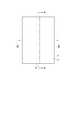
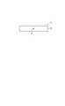
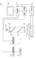
このような多光子吸収を利用する本実施形態に係るレーザ加工の原理について図1〜図6を用いて説明する。図1はレーザ加工中の加工対象物1の平面図であり、図2は図1に示す加工対象物1のII−II線に沿った断面図であり、図3はレーザ加工後の加工対象物1の平面図であり、図4は図3に示す加工対象物1のIV−IV線に沿った断面図であり、図5は図3に示す加工対象物1のV−V線に沿った断面図であり、図6は切断された加工対象物1の平面図である。The principle of laser processing according to this embodiment using such multiphoton absorption will be described with reference to FIGS. FIG. 1 is a plan view of a
図1及び図2に示すように、加工対象物1の表面3には切断予定ライン5がある。切断予定ライン5は直線状に延びた仮想線である。本実施形態に係るレーザ加工は、多光子吸収が生じる条件で加工対象物1の内部に集光点Pを合わせてレーザ光Lを加工対象物1に照射して改質領域7を形成する。なお、集光点とはレーザ光Lが集光した箇所のことである。As shown in FIGS. 1 and 2, the
レーザ光Lを切断予定ライン5に沿って(すなわち矢印A方向に沿って)相対的に移動させることにより、集光点Pを切断予定ライン5に沿って移動させる。これにより、図3〜図5に示すように改質領域7が切断予定ライン5に沿って加工対象物1の内部にのみ形成される。本実施形態に係るレーザ加工方法は、加工対象物1がレーザ光Lを吸収することにより加工対象物1を発熱させて改質領域7を形成するのではない。加工対象物1にレーザ光Lを透過させ加工対象物1の内部に多光子吸収を発生させて改質領域7を形成している。よって、加工対象物1の表面3ではレーザ光Lがほとんど吸収されないので、加工対象物1の表面3が溶融することはない。The condensing point P is moved along the
加工対象物1の切断において、切断する箇所に起点があると加工対象物1はその起点から割れるので、図6に示すように比較的小さな力で加工対象物1を切断することができる。よって、加工対象物1の表面3に不必要な割れを発生させることなく加工対象物1の切断が可能となる。In the cutting of the
なお、改質領域を起点とした加工対象物の切断は、次の二通りが考えられる。一つは、改質領域形成後、加工対象物に人為的な力が印加されることにより、改質領域を起点として加工対象物が割れ、加工対象物が切断される場合である。これは、例えば加工対象物の厚みが大きい場合の切断である。人為的な力が印加されるとは、例えば、加工対象物の切断予定ラインに沿って加工対象物に曲げ応力やせん断応力を加えたり、加工対象物に温度差を与えることにより熱応力を発生させたりすることである。他の一つは、改質領域を形成することにより、改質領域を起点として加工対象物の断面方向(厚さ方向)に向かって自然に割れ、結果的に加工対象物が切断される場合である。これは、例えば加工対象物の厚みが小さい場合、厚さ方向に改質領域が1つでも可能であり、加工対象物の厚みが大きい場合、厚さ方向に複数の改質領域を形成することで可能となる。なお、この自然に割れる場合も、切断する箇所の表面上において、改質領域が形成されていない部分まで割れが先走ることがなく、改質部を形成した部分のみを割断することができるので、割断を制御よくすることができる。近年、シリコンウェハ等の半導体ウェハの厚さは薄くなる傾向にあるので、このような制御性のよい割断方法は大変有効である。In addition, the following two kinds of cutting | disconnection of the processing target object from the modification | reformation area | region can be considered. One is a case where, after the modified region is formed, an artificial force is applied to the workpiece, so that the workpiece is cracked and the workpiece is cut from the modified region as a starting point. This is, for example, cutting when the thickness of the workpiece is large. When artificial force is applied, for example, bending stress or shear stress is applied to the workpiece along the planned cutting line of the workpiece, or thermal stress is generated by giving a temperature difference to the workpiece. It is to let you. The other is that when the modified region is formed, the modified region starts as a starting point, and naturally breaks in the cross-sectional direction (thickness direction) of the workpiece, resulting in the workpiece being cut. It is. For example, when the thickness of the workpiece is small, even one modified region is possible in the thickness direction, and when the thickness of the workpiece is large, a plurality of modified regions are formed in the thickness direction. Is possible. In addition, even when this breaks naturally, on the surface of the portion to be cut, the crack does not run to the part where the modified region is not formed, and only the part where the modified part is formed can be cleaved, The cleaving can be controlled well. In recent years, since the thickness of a semiconductor wafer such as a silicon wafer tends to be thin, such a cleaving method with good controllability is very effective.
さて、本実施形態において多光子吸収により形成される改質領域として、次の(1)〜(3)がある。
(1)改質領域が一つ又は複数のクラックを含むクラック領域の場合レーザ光を加工対象物(例えばガラスやLiTaO3からなる圧電材料)の内部に集光点を合わせて、集光点における電界強度が1×10⁸(W/cm2)以上でかつパルス幅が1μs以下の条件で照射する。このパルス幅の大きさは、多光子吸収を生じさせつつ加工対象物表面に余計なダメージを与えずに、加工対象物の内部にのみクラック領域を形成できる条件である。これにより、加工対象物の内部には多光子吸収による光学的損傷という現象が発生する。この光学的損傷により加工対象物の内部に熱ひずみが誘起され、これにより加工対象物の内部にクラック領域が形成される。電界強度の上限値としては、例えば1×1012(W/cm2)である。パルス幅は例えば1ns〜200nsが好ましい。なお、多光子吸収によるクラック領域の形成は、例えば、第45回レーザ熱加工研究会論文集(1998年.12月)の第23頁〜第28頁の「固体レーザー高調波によるガラス基板の内部マーキング」に記載されている。As modified regions formed by multiphoton absorption in this embodiment, there are the following (1) to (3).
(1) When the modified region is a crack region including one or more cracks The laser beam is focused on the inside of the workpiece (eg, piezoelectric material made of glass or LiTaO3), and the electric field at the focal point Irradiation is performed under conditions where the intensity is 1 × 10⁸ (W / cm2 ) or more and the pulse width is 1 μs or less. The magnitude of the pulse width is a condition that a crack region can be formed only inside the workpiece without causing extra damage to the workpiece surface while causing multiphoton absorption. As a result, a phenomenon of optical damage due to multiphoton absorption occurs inside the workpiece. This optical damage induces thermal strain inside the workpiece, thereby forming a crack region inside the workpiece. The upper limit value of the electric field strength is, for example, 1 × 10¹² (W / cm2 ). The pulse width is preferably 1 ns to 200 ns, for example. The formation of the crack region by multiphoton absorption is described in, for example, “Inside of glass substrate by solid-state laser harmonics” on pages 23-28 of the 45th Laser Thermal Processing Research Papers (December 1998). It is described in “Marking”.
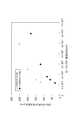
本発明者は、電界強度とクラックの大きさとの関係を実験により求めた。実験条件は次ぎの通りである。
(A)加工対象物:パイレックス(登録商標)ガラス(厚さ700μm)
(B)レーザ光源:半導体レーザ励起Nd:YAGレーザ波長:1064nmレーザ光スポット断面積:3.14×10⁻⁸cm2発振形態:Qスイッチパルス繰り返し周波数:100kHzパルス幅:30ns出力:出力<1mJ/パルスレーザ光品質:TEM00偏光特性:直線偏光(C)集光用レンズレーザ光波長に対する透過率:60パーセント(D)加工対象物が載置される載置台の移動速度:100mm/秒なお、レーザ光品質がTEM00とは、集光性が高くレーザ光の波長程度まで集光可能を意味する。The inventor obtained the relationship between the electric field strength and the size of the cracks by experiment. The experimental conditions are as follows.
(A) Workpiece: Pyrex (registered trademark) glass (thickness 700 μm)
(B) Laser light source: Semiconductor laser excitation Nd: YAG laser wavelength: 1064 nm Laser light spot cross-sectional area: 3.14 × 10⁻⁸ cm2 Oscillation form: Q switch pulse repetition frequency: 100 kHz Pulse width: 30 ns Output: Output <1 mJ / Pulse laser beam quality: TEM00 Polarization characteristics: Linearly polarized light (C) Condensation lens Transmittance with respect to laser beam wavelength: 60% (D) Moving speed of mounting table on which workpiece is mounted: 100 mm / second The laser light quality TEM00 means that the light condensing property is high and the light can be condensed to the wavelength of the laser light.
図7は上記実験の結果を示すグラフである。横軸はピークパワー密度であり、レーザ光がパルスレーザ光なので電界強度はピークパワー密度で表される。縦軸は1パルスのレーザ光により加工対象物の内部に形成されたクラック部分(クラックスポット)の大きさを示している。クラックスポットが集まりクラック領域となる。クラックスポットの大きさは、クラックスポットの形状のうち最大の長さとなる部分の大きさである。グラフ中の黒丸で示すデータは集光用レンズ(C)の倍率が100倍、開口数(NA)が0.80の場合である。一方、グラフ中の白丸で示すデータは集光用レンズ(C)の倍率が50倍、開口数(NA)が0.55の場合である。ピークパワー密度が1011(W/cm2)程度から加工対象物の内部にクラックスポットが発生し、ピークパワー密度が大きくなるに従いクラックスポットも大きくなることが分かる。FIG. 7 is a graph showing the results of the experiment. The horizontal axis represents the peak power density. Since the laser beam is a pulsed laser beam, the electric field strength is represented by the peak power density. The vertical axis represents the size of a crack portion (crack spot) formed inside the workpiece by one pulse of laser light. Crack spots gather to form a crack region. The size of the crack spot is the size of the portion having the maximum length in the shape of the crack spot. The data indicated by the black circles in the graph is when the magnification of the condenser lens (C) is 100 times and the numerical aperture (NA) is 0.80. On the other hand, the data indicated by white circles in the graph is when the magnification of the condenser lens (C) is 50 times and the numerical aperture (NA) is 0.55. From the peak power density of about 1011 (W / cm2 ), it can be seen that a crack spot is generated inside the workpiece, and the crack spot increases as the peak power density increases.
次に、本実施形態に係るレーザ加工において、クラック領域形成による加工対象物の切断のメカニズムについて図8〜図11を用いて説明する。図8に示すように、多光子吸収が生じる条件で加工対象物1の内部に集光点Pを合わせてレーザ光Lを加工対象物1に照射して切断予定ラインに沿って内部にクラック領域9を形成する。クラック領域9は一つ又は複数のクラックを含む領域である。図9に示すようにクラック領域9を起点としてクラックがさらに成長し、図10に示すようにクラックが加工対象物1の表面3と裏面21に到達し、図11に示すように加工対象物1が割れることにより加工対象物1が切断される。加工対象物の表面と裏面に到達するクラックは自然に成長する場合もあるし、加工対象物に力が印加されることにより成長する場合もある。Next, in the laser processing according to the present embodiment, a mechanism for cutting a workpiece by forming a crack region will be described with reference to FIGS. As shown in FIG. 8, the laser beam L is irradiated to the
(2)改質領域が溶融処理領域の場合レーザ光を加工対象物(例えばシリコンのような半導体材料)の内部に集光点を合わせて、集光点における電界強度が1×10⁸(W/cm2)以上でかつパルス幅が1μs以下の条件で照射する。これにより加工対象物の内部は多光子吸収によって局所的に加熱される。この加熱により加工対象物の内部に溶融処理領域が形成される。溶融処理領域とは一旦溶融後再固化した領域、溶融状態中の領域及び溶融から再固化する状態中の領域のうち少なくともいずれか一つを意味する。また、溶融処理領域は一旦溶融後再固化した領域であり、相変化した領域や結晶構造が変化した領域ということもできる。また、溶融処理領域とは単結晶構造、非晶質構造、多結晶構造において、ある構造が別の構造に変化した領域ということもできる。つまり、例えば、単結晶構造から非晶質構造に変化した領域、単結晶構造から多結晶構造に変化した領域、単結晶構造から非晶質構造及び多結晶構造を含む構造に変化した領域を意味する。加工対象物がシリコン単結晶構造の場合、溶融処理領域は例えば非晶質シリコン構造である。なお、電界強度の上限値としては、例えば1×1012(W/cm2)である。パルス幅は例えば1ns〜200nsが好ましい。(2) When the modified region is a melt-processed region A laser beam is focused on the inside of a workpiece (for example, a semiconductor material such as silicon), and the electric field intensity at the focused point is 1 × 10⁸ (W / cm2 ) or more and the pulse width is 1 μs or less. As a result, the inside of the workpiece is locally heated by multiphoton absorption. By this heating, a melt processing region is formed inside the workpiece. The melting treatment region means at least one of a region once solidified after melting, a region in a molten state, and a region in a state of being resolidified from melting. Further, the melting treatment region is a region once solidified after being melted, and can also be referred to as a phase-changed region or a region where the crystal structure has changed. The melt treatment region can also be said to be a region in which one structure is changed to another structure in a single crystal structure, an amorphous structure, or a polycrystalline structure. In other words, for example, a region changed from a single crystal structure to an amorphous structure, a region changed from a single crystal structure to a polycrystalline structure, or a region changed from a single crystal structure to a structure including an amorphous structure and a polycrystalline structure. To do. When the object to be processed has a silicon single crystal structure, the melt processing region has, for example, an amorphous silicon structure. The upper limit value of the electric field strength is, for example, 1 × 10¹² (W / cm2 ). The pulse width is preferably 1 ns to 200 ns, for example.
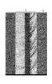
本発明者は、シリコンウェハの内部で溶融処理領域が形成されることを実験により確認した。実験条件は次ぎの通りである。The inventor has confirmed through experiments that a melt-processed region is formed inside a silicon wafer. The experimental conditions are as follows.
(A)加工対象物:シリコンウェハ(厚さ350μm、外径4インチ)
(B)レーザ光源:半導体レーザ励起Nd:YAGレーザ波長:1064nmレーザ光スポット断面積:3.14×10⁻⁸cm2発振形態:Qスイッチパルス繰り返し周波数:100kHzパルス幅:30ns出力:20μJ/パルスレーザ光品質:TEM00偏光特性:直線偏光(C)集光用レンズ倍率:50倍NA:0.55レーザ光波長に対する透過率:60パーセント(D)加工対象物が載置される載置台の移動速度:100mm/秒図12は上記条件でのレーザ加工により切断されたシリコンウェハの一部における断面の写真を表した図である。シリコンウェハ11の内部に溶融処理領域13が形成されている。なお、上記条件により形成された溶融処理領域の厚さ方向の大きさは100μm程度である。(A) Object to be processed: silicon wafer (thickness 350 μm, outer diameter 4 inches)
(B) Laser light source: semiconductor laser excitation Nd: YAG laser wavelength: 1064 nm Laser light spot cross-sectional area: 3.14 × 10⁻⁸ cm2 Oscillation form: Q switch pulse repetition frequency: 100 kHz pulse width: 30 ns output: 20 μJ / pulse Laser light quality: TEM00 polarization characteristics: linearly polarized light (C) Condensing lens magnification: 50 times NA: 0.55 Transmittance to laser light wavelength: 60% (D) Movement of the mounting table on which the workpiece is placed Speed: 100 mm / second FIG. 12 is a view showing a photograph of a cross section of a part of a silicon wafer cut by laser processing under the above conditions. A
溶融処理領域13が多光子吸収により形成されたことを説明する。図13は、レーザ光の波長とシリコン基板の内部の透過率との関係を示すグラフである。ただし、シリコン基板の表面側と裏面側それぞれの反射成分を除去し、内部のみの透過率を示している。シリコン基板の厚みtが50μm、100μm、200μm、500μm、1000μmの各々について上記関係を示した。The fact that the
例えば、Nd:YAGレーザの波長である1064nmにおいて、シリコン基板の厚みが500μm以下の場合、シリコン基板の内部ではレーザ光が80%以上透過することが分かる。図12に示すシリコンウェハ11の厚さは350μmであるので、多光子吸収による溶融処理領域はシリコンウェハの中心付近、つまり表面から175μmの部分に形成される。この場合の透過率は、厚さ200μmのシリコンウェハを参考にすると、90%以上なので、レーザ光がシリコンウェハ11の内部で吸収されるのは僅かであり、ほとんどが透過する。このことは、シリコンウェハ11の内部でレーザ光が吸収されて、溶融処理領域がシリコンウェハ11の内部に形成(つまりレーザ光による通常の加熱で溶融処理領域が形成)されたものではなく、溶融処理領域が多光子吸収により形成されたことを意味する。多光子吸収による溶融処理領域の形成は、例えば、溶接学会全国大会講演概要第66集(2000年4月)の第72頁〜第73頁の「ピコ秒パルスレーザによるシリコンの加工特性評価」に記載されている。For example, at a Nd: YAG laser wavelength of 1064 nm, when the thickness of the silicon substrate is 500 μm or less, it can be seen that 80% or more of the laser light is transmitted inside the silicon substrate. Since the thickness of the
なお、シリコンウェハは、溶融処理領域を起点として断面方向に向かって割れを発生させ、その割れがシリコンウェハの表面と裏面に到達することにより、結果的に切断される。シリコンウェハの表面と裏面に到達するこの割れは自然に成長する場合もあるし、加工対象物に力が印加されることにより成長する場合もある。なお、溶融処理領域からシリコンウェハの表面と裏面に割れが自然に成長するのは、一旦溶融後再固化した状態となった領域から割れが成長する場合、溶融状態の領域から割れが成長する場合及び溶融から再固化する状態の領域から割れが成長する場合のうち少なくともいずれか一つである。いずれの場合も切断後の切断面は図12に示すように内部にのみ溶融処理領域が形成される。加工対象物の内部に溶融処理領域を形成する場合、割断時、切断予定ラインから外れた不必要な割れが生じにくいので、割断制御が容易となる。In addition, a silicon wafer is cut | disconnected as a result by generating a crack toward a cross-sectional direction starting from the melt processing region and reaching the front and back surfaces of the silicon wafer. The cracks that reach the front and back surfaces of the silicon wafer may grow naturally or may grow by applying force to the workpiece. In addition, the crack grows naturally from the melt processing area to the front and back surfaces of the silicon wafer when the crack grows from the area once solidified after being melted, or when the crack grows from the melted area. And at least one of the cases where cracks grow from a region in a state of being resolidified from melting. In either case, the cut surface after cutting is formed with a melt treatment region only inside as shown in FIG. In the case where the melt processing region is formed inside the object to be processed, since the unnecessary cracks that are off the planned cutting line are not easily generated at the time of cleaving, cleaving control is facilitated.
(3)改質領域が屈折率変化領域の場合レーザ光を加工対象物(例えばガラス)の内部に集光点を合わせて、集光点における電界強度が1×10⁸(W/cm2)以上でかつパルス幅が1ns以下の条件で照射する。パルス幅を極めて短くして、多光子吸収を加工対象物の内部に起こさせると、多光子吸収によるエネルギーが熱エネルギーに転化せずに、加工対象物の内部にはイオン価数変化、結晶化又は分極配向等の永続的な構造変化が誘起されて屈折率変化領域が形成される。電界強度の上限値としては、例えば1×1012(W/cm2)である。パルス幅は例えば1ns以下が好ましく、1ps以下がさらに好ましい。多光子吸収による屈折率変化領域の形成は、例えば、第42回レーザ熱加工研究会論文集(1997年.11月)の第105頁〜第111頁の「フェムト秒レーザー照射によるガラス内部への光誘起構造形成」に記載されている。(3) When the modified region is a refractive index changing region The laser beam is focused on the inside of the object to be processed (eg, glass), and the electric field strength at the focused point is 1 × 10⁸ (W / cm2 ). Irradiation is performed under the above conditions with a pulse width of 1 ns or less. When the pulse width is made extremely short and multiphoton absorption occurs inside the workpiece, the energy due to the multiphoton absorption is not converted into thermal energy, and the ion valence change and crystallization occur inside the workpiece. Alternatively, a permanent structural change such as polarization orientation is induced to form a refractive index change region. The upper limit value of the electric field strength is, for example, 1 × 10¹² (W / cm2 ). For example, the pulse width is preferably 1 ns or less, and more preferably 1 ps or less. The formation of the refractive index changing region by multiphoton absorption is described in, for example, “The Femtosecond Laser Irradiation to the Inside of Glass” on
以上のように本実施形態によれば、改質領域を多光子吸収により形成している。そして、本実施形態は、パルスレーザ光の繰り返し周波数の大きさやパルスレーザ光の集光点の相対的移動速度の大きさを調節することにより、1パルスのパルスレーザ光で形成される改質スポットと次の1パルスのパルスレーザ光で形成される改質スポットとの距離を制御している。つまり隣り合う改質スポット間の距離を制御している。以下この距離をピッチpとして説明をする。ピッチpの制御についてクラック領域を例に説明する。As described above, according to the present embodiment, the modified region is formed by multiphoton absorption. And this embodiment adjusts the magnitude | size of the repetition frequency of a pulse laser beam, and the magnitude | size of the relative moving speed of the condensing point of a pulse laser beam, and the modification spot formed with a pulse laser beam of 1 pulse. And the modified spot formed by the next pulse laser beam of one pulse is controlled. That is, the distance between adjacent reforming spots is controlled. Hereinafter, this distance will be described as the pitch p. The control of the pitch p will be described taking a crack region as an example.
パルスレーザ光の繰り返し周波数をf(Hz)、加工対象物のX軸ステージ又はY軸ステージの移動速度をv(mm/sec)とする。これらのステージの移動速度はパルスレーザ光の集光点の相対的移動の速度の一例である。パルスレーザ光の1ショットで形成されるクラック部分をクラックスポットという。よって、切断予定ライン5の単位長さあたりに形成されるクラックスポットの数nは、以下の通りである。
n=f/v単位長さあたりに形成されるクラックスポットの数nの逆数がピッチpに相当する。
p=1/nThe repetition frequency of the pulse laser beam is f (Hz), and the moving speed of the X-axis stage or Y-axis stage of the workpiece is v (mm / sec). The moving speed of these stages is an example of the relative moving speed of the condensing point of the pulse laser beam. A crack portion formed by one shot of pulsed laser light is called a crack spot. Therefore, the number n of crack spots formed per unit length of the planned
The reciprocal of the number n of crack spots formed per unit length of n = f / v corresponds to the pitch p.
p = 1 / n
よって、パルスレーザ光の繰り返し周波数の大きさ及びパルスレーザ光の集光点の相対的移動速度の大きさのうち少なくともいずれかを調節すれば、ピッチpを制御することができる。すなわち、繰り返し周波数をf(Hz)を大きくすることやステージの移動速度をv(mm/sec)を小さくすることにより、ピッチpを小さく制御できる。逆に、繰り返し周波数をf(Hz)を小さくすることやステージの移動速度をv(mm/sec)を大きくすることにより、ピッチpを大きく制御できる。Therefore, the pitch p can be controlled by adjusting at least one of the repetition frequency of the pulsed laser light and the relative moving speed of the focused point of the pulsed laser light. That is, the pitch p can be controlled to be small by increasing the repetition frequency f (Hz) and decreasing the stage moving speed v (mm / sec). Conversely, the pitch p can be largely controlled by decreasing the repetition frequency f (Hz) and increasing the stage moving speed v (mm / sec).
ところで、ピッチpと切断予定ライン5方向におけるクラックスポットの寸法dとの関係は図14〜図16に示す三通りがある。図14〜図16は、本実施形態に係るレーザ加工によりクラック領域が形成された加工対象物の切断予定ライン5に沿った部分の平面図である。クラックスポット90は1パルスのパルスレーザ光で形成される。複数のクラックスポット90が切断予定ライン5に沿って並ぶように形成されることにより、クラック領域9が形成される。By the way, there are three relations between the pitch p and the crack spot dimension d in the direction of the cutting scheduled
図14は、ピッチpが寸法dより大きい場合を示している。クラック領域9は切断予定ライン5に沿って加工対象物の内部に断続的に形成されている。図15は、ピッチpが寸法dと略等しい場合を示している。クラック領域9は切断予定ライン5に沿って加工対象物の内部に連続に形成されている。図16は、ピッチpが寸法dより小さい場合を示している。クラック領域9は切断予定ライン5に沿って加工対象物の内部に連続的に形成されている。FIG. 14 shows a case where the pitch p is larger than the dimension d. The
図14によれば、クラック領域9が切断予定ライン5に沿って連続していないので、切断予定ライン5の箇所はある程度の強度を保持している。よって、レーザ加工終了後に加工対象物の切断工程を行う場合、加工対象物のハンドリングが容易となる。図15及び図16によれば、クラック領域9が切断予定ライン5に沿って連続的に形成されているので、クラック領域9を起点とした加工対象物の切断が容易となる。According to FIG. 14, since the
図14によればピッチpが寸法dより大きくされており、図15によればピッチpを寸法dと略等しくされているので、パルスレーザ光の照射により多光子吸収の生じる領域が既に形成されたクラックスポット90と重なるのを防止できる。この結果、クラックスポットの寸法のばらつきを小さくすることができる。すなわち、本発明者によれば、パルスレーザ光の照射により多光子吸収の生じる領域が既に形成されたクラックスポット90と重なると、この領域に形成されるクラックスポット90の寸法のばらつきが大きくなる、ことが分かった。クラックスポット90の寸法のばらつきが大きくなると、加工対象物を切断予定ラインに沿って精密に切断するのが困難となり、また、切断面の平坦性も悪くなる。図14及び図15によれば、クラックスポットの寸法のばらつきを小さくできるので、切断予定ラインに沿って加工対象物を精密に切断することができ、かつ、切断面を平坦にすることができる。According to FIG. 14, the pitch p is made larger than the dimension d, and according to FIG. 15, the pitch p is made substantially equal to the dimension d, so that a region where multiphoton absorption occurs is already formed by the irradiation of the pulse laser beam. It is possible to prevent the
以上説明したように、本実施形態によれば、パルスレーザ光の繰り返し周波数の大きさやパルスレーザ光の集光点の相対的移動速度の大きさを調節することにより、ピッチpを制御することができる。これにより、加工対象物の厚さや材質等を考慮してピッチpを変えることにより、加工対象物に応じたレーザ加工が可能となる。As described above, according to the present embodiment, the pitch p can be controlled by adjusting the magnitude of the repetition frequency of the pulse laser light and the magnitude of the relative movement speed of the focal point of the pulse laser light. it can. As a result, by changing the pitch p in consideration of the thickness and material of the workpiece, laser processing according to the workpiece can be performed.
なお、ピッチpの制御ができることについて、クラックスポットの場合で説明したが、溶融処理スポットや屈折率変化スポットでも同様のことが言える。但し、溶融処理スポットや屈折率変化スポットについてはすでに形成された溶融処理スポットや屈折率変化スポットとの重なりが生じても問題はない。また、パルスレーザ光の集光点の相対的移動とは、パルスレーザ光の集光点を固定して加工対象物を移動させる場合でもよいし、加工対象物を固定してパルスレーザ光の集光点を移動させる場合でもよいし、加工対象物とパルスレーザ光の集光点とを互いに逆方向に移動させる場合でもよいし、加工対象物とパルスレーザ光の集光点とを速度を異ならせかつ同じ方向に移動させる場合でもよい。The control of the pitch p has been described in the case of a crack spot, but the same can be said for a melting treatment spot and a refractive index change spot. However, there is no problem even if the melt processing spot and the refractive index change spot overlap with the already formed melt processing spot and the refractive index change spot. The relative movement of the focused point of the pulsed laser beam may be a case where the focused object of the pulsed laser beam is fixed and the object to be processed is moved, or the focused object of the pulsed laser beam is collected while the processed object is fixed. The light spot may be moved, the object to be processed and the focused point of the pulse laser light may be moved in opposite directions, or the speed of the processed object and the focused point of the pulse laser light may be different. And may be moved in the same direction.
次に、本実施形態に係るレーザ加工装置について説明する。図17はこのレーザ加工装置100の概略構成図である。レーザ加工装置100は、レーザ光Lを発生するレーザ光源101と、レーザ光Lの出力やパルス幅等を調節するためにレーザ光源101を制御するレーザ光源制御部102と、レーザ光Lの反射機能を有しかつレーザ光Lの光軸の向きを90°変えるように配置されたダイクロイックミラー103と、ダイクロイックミラー103で反射されたレーザ光Lを集光する集光用レンズ105と、集光用レンズ105で集光されたレーザ光Lが照射される加工対象物1が載置される載置台107と、載置台107をX軸方向に移動させるためのX軸ステージ109と、載置台107をX軸方向に直交するY軸方向に移動させるためのY軸ステージ111と、載置台107をX軸及びY軸方向に直交するZ軸方向に移動させるためのZ軸ステージ113と、これら三つのステージ109,111,113の移動を制御するステージ制御部115と、を備える。Next, the laser processing apparatus according to this embodiment will be described. FIG. 17 is a schematic configuration diagram of the
レーザ光源101はパルスレーザ光を発生するNd:YAGレーザである。レーザ光源101に用いることができるレーザとして、この他、Nd:YVO4レーザやNd:YLFレーザやチタンサファイアレーザがある。クラック領域や溶融処理領域を形成する場合、Nd:YAGレーザ、Nd:YVO4レーザ、Nd:YLFレーザを用いるのが好適である。屈折率変化領域を形成する場合、チタンサファイアレーザを用いるのが好適である。The
レーザ光源101はQスイッチレーザである。図18は、レーザ光源101に備えられるQスイッチレーザの概略構成図である。Qスイッチレーザは、所定間隔を設けて配置されたミラー51,53と、ミラー51とミラー53との間に配置されたレーザ媒質55と、レーザ媒質55に励起用の入力を加える励起源57、レーザ媒質55とミラー51との間に配置されたQスイッチ59と、を備える。レーザ媒質55の材料は例えばNd:YAGである。The
Qスイッチ59を利用して共振器の損失を高くした状態で励起源57から励起入力をレーザ媒質55に加えることにより、レーザ媒質55の反転分布を所定値まで上昇させる。その後、Qスイッチ59を利用して共振器の損失を低くした状態にすることにより、蓄積されたエネルギーを瞬時に発振させパルスレーザ光Lを発生させる。レーザ光源制御部102からの信号S(例えば超音波パルスの繰り返し周波数の変化)によりQスイッチ59が高い状態になるように制御される。よって、レーザ光源制御部102からの信号Sにより、レーザ光源101から出射されるパルスレーザ光Lの繰り返し周波数を調節することができる。レーザ光源制御部102が周波数調節手段の一例となる。繰り返し周波数の調節は、レーザ加工装置の操作者が後で説明する全体制御部127にキーボード等を用いて繰り返し周波数の大きさを入力することによりなされる。以上がレーザ光源101の詳細である。By applying excitation input from the
レーザ加工中、加工対象物1をX軸方向やY軸方向に移動させることにより、切断予定ラインに沿って改質領域を形成する。よって、例えば、X軸方向に改質領域を形成する場合、X軸ステージ109の移動速度を調節することにより、パルスレーザ光の集光点の相対的移動の速度を調節することができる。また、Y軸方向に改質領域を形成する場合、Y軸ステージ111の移動速度を調節することにより、パルスレーザ光の集光点の相対的移動の速度を調節することができる。これらのステージの移動速度の調節はステージ制御部115により制御される。ステージ制御部115は速度調節手段の一例となる。速度の調節は、レーザ加工装置の操作者が後で説明する全体制御部127にキーボード等を用いて速度の大きさを入力することによりなされる。なお、集光点Pを移動可能とし、その移動速度を調節することにより、パルスレーザ光の集光点の相対的移動の速度を調節することもできる。During the laser processing, the modified object is formed along the planned cutting line by moving the
Z軸方向は加工対象物1の表面3と直交する方向なので、加工対象物1に入射するレーザ光Lの焦点深度の方向となる。よって、Z軸ステージ113をZ軸方向に移動させることにより、加工対象物1の内部にレーザ光Lの集光点Pを合わせることができる。また、この集光点PのX(Y)軸方向の移動は、加工対象物1をX(Y)軸ステージ109(111)によりX(Y)軸方向に移動させることにより行う。X(Y)軸ステージ109(111)が移動手段の一例となる。Since the Z-axis direction is a direction orthogonal to the
集光用レンズ105は集光手段の一例である。Z軸ステージ113はレーザ光の集光点を加工対象物の内部に合わせる手段の一例である。集光用レンズ105をZ軸方向に移動させることによっても、レーザ光の集光点を加工対象物の内部に合わせることができる。The condensing
レーザ加工装置100はさらに、載置台107に載置された加工対象物1を可視光線により照明するために可視光線を発生する観察用光源117と、ダイクロイックミラー103及び集光用レンズ105と同じ光軸上に配置された可視光用のビームスプリッタ119と、を備える。ビームスプリッタ119と集光用レンズ105との間にダイクロイックミラー103が配置されている。ビームスプリッタ119は、可視光線の約半分を反射し残りの半分を透過する機能を有しかつ可視光線の光軸の向きを90°変えるように配置されている。観察用光源117から発生した可視光線はビームスプリッタ119で約半分が反射され、この反射された可視光線がダイクロイックミラー103及び集光用レンズ105を透過し、加工対象物1の切断予定ライン5等を含む表面3を照明する。The
レーザ加工装置100はさらに、ビームスプリッタ119、ダイクロイックミラー103及び集光用レンズ105と同じ光軸上に配置された撮像素子121及び結像レンズ123を備える。撮像素子121としては例えばCCD(charge-coupled device)カメラがある。切断予定ライン5等を含む表面3を照明した可視光線の反射光は、集光用レンズ105、ダイクロイックミラー103、ビームスプリッタ119を透過し、結像レンズ123で結像されて撮像素子121で撮像され、撮像データとなる。The
レーザ加工装置100はさらに、撮像素子121から出力された撮像データが入力される撮像データ処理部125と、レーザ加工装置100全体を制御する全体制御部127と、モニタ129と、を備える。撮像データ処理部125は、撮像データを基にして観察用光源117で発生した可視光の焦点が表面3上に合わせるための焦点データを演算する。この焦点データを基にしてステージ制御部115がZ軸ステージ113を移動制御することにより、可視光の焦点が表面3に合うようにする。よって、撮像データ処理部125はオートフォーカスユニットとして機能する。また、撮像データ処理部125は、撮像データを基にして表面3の拡大画像等の画像データを演算する。この画像データは全体制御部127に送られ、全体制御部で各種処理がなされ、モニタ129に送られる。これにより、モニタ129に拡大画像等が表示される。The
全体制御部127には、ステージ制御部115からのデータ、撮像データ処理部125からの画像データ等が入力し、これらのデータも基にしてレーザ光源制御部102、観察用光源117及びステージ制御部115を制御することにより、レーザ加工装置100全体を制御する。よって、全体制御部127はコンピュータユニットとして機能する。Data from the
図19は全体制御部127の一例の一部分を示すブロック図である。全体制御部127は距離演算部141、寸法記憶部143及び画像作成部145を備える。距離演算部141には、パルスレーザ光の繰り返し周波数の大きさ及びステージ109、111の移動速度の大きさが入力される。これらの入力はレーザ加工装置の操作者がキーボード等を用いて行う。FIG. 19 is a block diagram illustrating a part of an example of the
距離演算部141は上述した式(n=f/v,p=1/n)を利用して隣り合う改質スポット間の距離(ピッチ)を演算する。距離演算部141は、この距離データをモニタ129に送る。これにより、モニタ129には入力された周波数の大きさ及び速度の大きさのもとで形成される改質スポット間の距離が表示される。The
また、この距離データは画像作成部145にも送られる。寸法記憶部143には予めこのレーザ加工装置で形成される改質スポットの寸法が記憶されている。画像作成部145は、この距離データと寸法記憶部143に記憶された寸法のデータとを基にして、この距離と寸法とにより形成される改質領域の画像データを作成しモニタ129に送る。これにより、モニタ129には改質領域の画像も表示される。よって、レーザ加工前に隣り合う改質スポット間の距離や改質領域の形状を知ることができる。The distance data is also sent to the
距離演算部141は式(n=f/v,p=1/n)を利用して改質スポット間の距離を演算しているが次のようにしてもよい。まず、繰り返し周波数の大きさとステージ109、111の移動速度と改質スポット間の距離との関係を予め登録したテーブルを作成し、このテーブルのデータを距離演算部141に記憶させる。繰り返し周波数の大きさ及びステージ109、111の移動速度の大きさが距離演算部141に入力されることにより、距離演算部141は上記テーブルの中からこれらの大きさの条件で形成される改質スポットにおける改質スポット間の距離を読み出す。The
なお、繰り返し周波数の大きさを固定しステージの移動速度の大きさを可変としてもよい。逆に、ステージの移動速度の大きさを固定し繰り返し周波数の大きさを可変としてもよい。これらの場合も距離演算部141において上述した式やテーブルを用いることにより、改質スポット間の距離や改質領域の画像をモニタ129に表示させるための処理を行う。Note that the magnitude of the repetition frequency may be fixed and the magnitude of the stage moving speed may be variable. Conversely, the stage moving speed may be fixed and the repetition frequency may be variable. In these cases, the
以上のように図19に示す全体制御部127では繰り返し周波数の大きさやステージの移動速度の大きさを入力することにより、隣り合う改質スポット間の距離を演算している。隣り合う改質スポット間の所望の距離を入力し、繰り返し周波数の大きさやステージの移動速度の大きさを制御してもよい。以下これについて説明する。As described above, the
図20は全体制御部127の他の例の一部分を示すブロック図である。全体制御部127は周波数演算部147を備える。レーザ加工装置の操作者はキーボード等により周波数演算部147に隣り合う改質スポット間の距離の大きさを入力する。この距離の大きさは、加工対象物の厚さや材質等を考慮して決定される。この入力により周波数演算部147は上記式やテーブルを基にして、この距離の大きさとなるための周波数を演算する。この例ではステージの移動速度は固定である。周波数演算部147は演算されたデータをレーザ光源制御部102に送る。この周波数の大きさに調節されたレーザ加工装置で加工対象物をレーザ加工することにより、隣り合う改質スポット間の距離を所望の大きさにすることができる。この周波数の大きさのデータはモニタ129にも送られ、この周波数の大きさが表示される。FIG. 20 is a block diagram illustrating a part of another example of the
図21は全体制御部127のさらに他の例の一部分を示すブロック図である。全体制御部127は速度演算部149を備える。上記と同様に隣り合う改質スポット間の距離の大きさが速度演算部149に入力される。この入力により速度演算部149は上記式やテーブルを基にして、この距離の大きさとなるためのステージ移動速度を演算する。この例では繰り返し周波数は固定である。速度演算部149は演算されたデータをステージ制御部115に送る。このステージ移動速度の大きさに調節されたレーザ加工装置で加工対象物をレーザ加工することにより、隣り合う改質スポット間の距離を所望の大きさにすることができる。このステージ移動速度の大きさのデータはモニタ129にも送られ、このステージ移動速度の大きさが表示される。FIG. 21 is a block diagram showing a part of still another example of the
図22は全体制御部127のさらに他の例の一部分を示すブロック図である。全体制御部127は組み合わせ演算部151を備える。図20及び図21の場合と異なる点は、繰り返し周波数及びステージ移動速度の両方が演算されることである。上記と同様に隣り合う改質スポット間の距離の大きさを組み合わせ演算部151に入力する。組み合わせ演算部151は上記式やテーブルを基にして、この距離の大きさとなるための繰り返し周波数及びステージ移動速度を演算する。FIG. 22 is a block diagram showing a part of still another example of the
組み合わせ演算部151は演算されたデータをレーザ光源制御部102及びステージ制御部115に送る。レーザ光源制御部102は演算された繰り返し周波数の大きさとなるようにレーザ光源101を調節する。ステージ制御部115は演算されたステージ移動速度の大きさとなるようにステージ109、111を調節する。これらの調節がなされたレーザ加工装置で加工対象物をレーザ加工することにより、隣り合う改質スポット間の距離を所望の大きさにすることができる。演算された繰り返し周波数の大きさ及びステージ移動速度の大きさのデータはモニタ129にも送られ、演算されたこれらの値が表示される。The
次に、図17及び図23を用いて、本実施形態に係るレーザ加工装置を用いたレーザ加工方法を説明する。図23は、このレーザ加工方法を説明するためのフローチャートである。加工対象物1はシリコンウェハである。Next, a laser processing method using the laser processing apparatus according to the present embodiment will be described with reference to FIGS. FIG. 23 is a flowchart for explaining this laser processing method. The
まず、加工対象物1の光吸収特性を図示しない分光光度計等により測定する。この測定結果に基づいて、加工対象物1に対して透明な波長又は吸収の少ない波長のレーザ光Lを発生するレーザ光源101を選定する(S101)。次に、加工対象物1の厚さを測定する。厚さの測定結果及び加工対象物1の屈折率を基にして、加工対象物1のZ軸方向の移動量を決定する(S103)。これは、レーザ光Lの集光点Pが加工対象物1の内部に位置させるために、加工対象物1の表面3に位置するレーザ光Lの集光点を基準とした加工対象物1のZ軸方向の移動量である。この移動量を全体制御部127に入力される。First, the light absorption characteristics of the
加工対象物1をレーザ加工装置100の載置台107に載置する。そして、観察用光源117から可視光を発生させて加工対象物1を照明する(S105)。照明された切断予定ライン5を含む加工対象物1の表面3を撮像素子121により撮像する。この撮像データは撮像データ処理部125に送られる。この撮像データに基づいて撮像データ処理部125は観察用光源117の可視光の焦点が表面3に位置するような焦点データを演算する(S107)。The
この焦点データはステージ制御部115に送られる。ステージ制御部115は、この焦点データを基にしてZ軸ステージ113をZ軸方向の移動させる(S109)。これにより、観察用光源117の可視光の焦点が表面3に位置する。なお、撮像データ処理部125は撮像データに基づいて、切断予定ライン5を含む加工対象物1の表面3の拡大画像データを演算する。この拡大画像データは全体制御部127を介してモニタ129に送られ、これによりモニタ129に切断予定ライン5付近の拡大画像が表示される。This focus data is sent to the
全体制御部127には予めステップS103で決定された移動量データが入力されており、この移動量データがステージ制御部115に送られる。ステージ制御部115はこの移動量データに基づいて、レーザ光Lの集光点Pが加工対象物1の内部となる位置に、Z軸ステージ113により加工対象物1をZ軸方向に移動させる(S111)。The movement amount data determined in advance in step S <b> 103 is input to the
次に、1パルスのパルスレーザで形成される溶融処理スポットにおける隣り合う溶融処理スポット間の距離、つまりピッチpの大きさを決定する(S112)。ピッチpは加工対象物1の厚さや材質等を考慮して決定される。ピッチpの大きさを図22に示す全体制御部127に入力する。Next, the distance between adjacent melt processing spots in the melt processing spot formed by one pulse laser, that is, the size of the pitch p is determined (S112). The pitch p is determined in consideration of the thickness and material of the
次に、レーザ光源101からレーザ光Lを発生させて、レーザ光Lを加工対象物1の表面3の切断予定ライン5に照射する。レーザ光Lの集光点Pは加工対象物1の内部に位置しているので、溶融処理領域は加工対象物1の内部にのみ形成される。そして、切断予定ライン5に沿うようにX軸ステージ109やY軸ステージ111を移動させて、溶融処理領域を切断予定ライン5に沿うように加工対象物1の内部に形成する(S113)。そして、加工対象物1を切断予定ライン5に沿って曲げることにより、加工対象物1を切断する(S115)。これにより、加工対象物1をシリコンチップに分割する。Next, the laser light L is generated from the
本実施形態の効果を説明する。これによれば、多光子吸収を起こさせる条件でかつ加工対象物1の内部に集光点Pを合わせて、パルスレーザ光Lを切断予定ライン5に照射している。そして、X軸ステージ109やY軸ステージ111を移動させることにより、集光点Pを切断予定ライン5に沿って移動させている。これにより、改質領域(例えばクラック領域、溶融処理領域、屈折率変化領域)を切断予定ライン5に沿うように加工対象物1の内部に形成している。加工対象物の切断する箇所に何らかの起点があると、加工対象物を比較的小さな力で割って切断することができる。よって、改質領域を起点として切断予定ライン5に沿って加工対象物1を割ることにより、比較的小さな力で加工対象物1を切断することができる。これにより、加工対象物1の表面3に切断予定ライン5から外れた不必要な割れを発生させることなく加工対象物1を切断することができる。The effect of this embodiment will be described. According to this, the pulse laser beam L is irradiated on the
また、本実施形態によれば、加工対象物1に多光子吸収を起こさせる条件でかつ加工対象物1の内部に集光点Pを合わせて、パルスレーザ光Lを切断予定ライン5に照射している。よって、パルスレーザ光Lは加工対象物1を透過し、加工対象物1の表面3ではパルスレーザ光Lがほとんど吸収されないので、改質領域形成が原因で表面3が溶融等のダメージを受けることはない。Moreover, according to this embodiment, the laser beam L is irradiated to the
以上説明したように本実施形態によれば、加工対象物1の表面3に切断予定ライン5から外れた不必要な割れや溶融が生じることなく、加工対象物1を切断することができる。よって、加工対象物1が例えば半導体ウェハの場合、半導体チップに切断予定ラインから外れた不必要な割れや溶融が生じることなく、半導体チップを半導体ウェハから切り出すことができる。表面に電極パターンが形成されている加工対象物や、圧電素子ウェハや液晶等の表示装置が形成されたガラス基板のように表面に電子デバイスが形成されている加工対象物についても同様である。よって、本実施形態によれば、加工対象物を切断することにより作製される製品(例えば半導体チップ、圧電デバイスチップ、液晶等の表示装置)の歩留まりを向上させることができる。As described above, according to the present embodiment, the
また、本実施形態によれば、加工対象物1の表面3の切断予定ライン5は溶融しないので、切断予定ライン5の幅(この幅は、例えば半導体ウェハの場合、半導体チップとなる領域同士の間隔である。)を小さくできる。これにより、一枚の加工対象物1から作製される製品の数が増え、製品の生産性を向上させることができる。Further, according to the present embodiment, since the
また、本実施形態によれば、加工対象物1の切断加工にレーザ光を用いるので、ダイヤモンドカッタを用いたダイシングよりも複雑な加工が可能となる。例えば、図24に示すように切断予定ライン5が複雑な形状であっても、本実施形態によれば切断加工が可能となる。これらの効果は後に説明する例でも同様である。Further, according to the present embodiment, since laser light is used for cutting the
また、本実施形態によれば、パルスレーザ光の繰り返し周波数の大きさの調節や、X軸ステージ109、Y軸ステージ111の移動速度の大きさの調節により、隣合う溶融処理スポットの距離を制御できる。加工対象物1の厚さや材質等を考慮して距離の大きさを変えることにより、目的に応じた加工が可能となる。In addition, according to the present embodiment, the distance between adjacent melt processing spots is controlled by adjusting the repetition frequency of the pulse laser beam and adjusting the moving speed of the
1・・・加工対象物、3・・・表面、5・・・切断予定ライン、7・・・改質領域、9・・・クラック領域、11・・・シリコンウェハ、13・・・溶融処理領域、90・・・クラックスポット、100・・・レーザ加工装置、101・・・レーザ光源、105・・・集光用レンズ、109・・・X軸ステージ、111・・・Y軸ステージ、113・・・Z軸ステージ、141・・・距離演算部、143・・・寸法記憶部、145・・・画像作成部、147・・・周波数演算部、149・・・速度演算部、151・・・組み合わせ演算部、P・・・集光点、p・・・クラックスポットのピッチ、d・・・クラックスポットの寸法DESCRIPTION OF
Claims (4)
Translated fromJapanese前記加工対象物の厚さ方向と略直交する断面において、隣り合う前記改質スポット間のピッチを、前記切断予定ラインに沿った方向の前記改質スポットの寸法よりも大きくすることにより、前記改質スポットを前記切断予定ラインに沿って前記加工対象物の内部に断続的に形成し、前記ウェハ状の加工対象物に形成された前記改質領域のみを起点として加工対象物を切断することを特徴とする加工対象物切断方法。By aligning the condensing point inside the wafer-like workpiece and irradiating a pulse laser beam having a pulse width of 1 μs or less, the workpiece is modified along the planned cutting line of the workpiece. Forming a plurality of quality spots, and forming a modified region serving as a starting point of cutting by the plurality of modified spots,
In the cross-section substantially perpendicular to the thickness direction of the workpiece, the pitch between adjacent modified spots is made larger than the dimension of the modified spots in the direction along the planned cutting line, thereby improving the modification. Forming a quality spot intermittently inside the workpiece along the planned cutting line, and cutting the workpiece from only the modified region formed in the wafer-like workpiece. A method for cutting an object to be processed.
The method according to claim 1, wherein the modified spot is a refractive index changing spot, and the modified area is a refractive index changing area.
Priority Applications (1)
| Application Number | Priority Date | Filing Date | Title |
|---|---|---|---|
| JP2009146690AJP4880722B2 (en) | 2000-09-13 | 2009-06-19 | Processing object cutting method |
Applications Claiming Priority (3)
| Application Number | Priority Date | Filing Date | Title |
|---|---|---|---|
| JP2000278306 | 2000-09-13 | ||
| JP2000278306 | 2000-09-13 | ||
| JP2009146690AJP4880722B2 (en) | 2000-09-13 | 2009-06-19 | Processing object cutting method |
Related Parent Applications (1)
| Application Number | Title | Priority Date | Filing Date |
|---|---|---|---|
| JP2001278707ADivisionJP4762458B2 (en) | 2000-09-13 | 2001-09-13 | Laser processing equipment |
Publications (2)
| Publication Number | Publication Date |
|---|---|
| JP2009214182Atrue JP2009214182A (en) | 2009-09-24 |
| JP4880722B2 JP4880722B2 (en) | 2012-02-22 |
Family
ID=18763489
Family Applications (4)
| Application Number | Title | Priority Date | Filing Date |
|---|---|---|---|
| JP2001277163AExpired - LifetimeJP4659300B2 (en) | 2000-09-13 | 2001-09-12 | Laser processing method and semiconductor chip manufacturing method |
| JP2009146690AExpired - LifetimeJP4880722B2 (en) | 2000-09-13 | 2009-06-19 | Processing object cutting method |
| JP2009146682AExpired - LifetimeJP4890594B2 (en) | 2000-09-13 | 2009-06-19 | Cutting method of workpiece |
| JP2011158040AExpired - LifetimeJP5138800B2 (en) | 2000-09-13 | 2011-07-19 | Laser processing method |
Family Applications Before (1)
| Application Number | Title | Priority Date | Filing Date |
|---|---|---|---|
| JP2001277163AExpired - LifetimeJP4659300B2 (en) | 2000-09-13 | 2001-09-12 | Laser processing method and semiconductor chip manufacturing method |
Family Applications After (2)
| Application Number | Title | Priority Date | Filing Date |
|---|---|---|---|
| JP2009146682AExpired - LifetimeJP4890594B2 (en) | 2000-09-13 | 2009-06-19 | Cutting method of workpiece |
| JP2011158040AExpired - LifetimeJP5138800B2 (en) | 2000-09-13 | 2011-07-19 | Laser processing method |
Country Status (12)
| Country | Link |
|---|---|
| US (21) | US6992026B2 (en) |
| EP (13) | EP2204255B1 (en) |
| JP (4) | JP4659300B2 (en) |
| KR (18) | KR101506429B1 (en) |
| CN (27) | CN101195190B (en) |
| AT (1) | ATE552064T1 (en) |
| AU (1) | AU2001286227A1 (en) |
| ES (5) | ES2526418T3 (en) |
| IL (1) | IL154910A0 (en) |
| SG (3) | SG2009061698A (en) |
| TW (2) | TWI250060B (en) |
| WO (1) | WO2002022301A1 (en) |
Cited By (17)
| Publication number | Priority date | Publication date | Assignee | Title |
|---|---|---|---|---|
| JP2011091322A (en)* | 2009-10-26 | 2011-05-06 | Toshiba Mach Co Ltd | Laser dicing method and laser dicing device |
| JP2011131256A (en)* | 2009-12-25 | 2011-07-07 | Mitsuboshi Diamond Industrial Co Ltd | Machining method of workpiece, dividing method of workpiece, and laser beam machining apparatus |
| JP2011147968A (en)* | 2010-01-21 | 2011-08-04 | Toshiba Mach Co Ltd | Laser dicing apparatus |
| JP2012006065A (en)* | 2010-06-28 | 2012-01-12 | Mitsuboshi Diamond Industrial Co Ltd | Laser machining device |
| JP2012006064A (en)* | 2010-06-28 | 2012-01-12 | Mitsuboshi Diamond Industrial Co Ltd | Method for machining workpiece, method for dividing workpiece and laser machining apparatus |
| JP2012006063A (en)* | 2010-06-28 | 2012-01-12 | Mitsuboshi Diamond Industrial Co Ltd | Method for machining workpiece and method for dividing the same |
| JP2012024815A (en)* | 2010-07-23 | 2012-02-09 | Mitsuboshi Diamond Industrial Co Ltd | Laser beam machining device, method for machining workpiece, and method for dividing the workpiece |
| JP2012024816A (en)* | 2010-07-23 | 2012-02-09 | Mitsuboshi Diamond Industrial Co Ltd | Laser beam machining device, method for machining workpiece, and method for dividing the workpiece |
| KR101146642B1 (en) | 2010-08-04 | 2012-05-16 | (주)큐엠씨 | Apparatus for Breaking Processed Object Using Curved Surface Close-adhesion |
| JP2012176443A (en)* | 2012-06-15 | 2012-09-13 | Mitsuboshi Diamond Industrial Co Ltd | Laser beam machining apparatus, method for machining workpiece and method for dividing workpiece |
| JP2012183590A (en)* | 2012-06-15 | 2012-09-27 | Mitsuboshi Diamond Industrial Co Ltd | Method for machining workpiece, method for dividing workpiece and laser beam machining device |
| JP2012210658A (en)* | 2012-06-15 | 2012-11-01 | Mitsuboshi Diamond Industrial Co Ltd | Laser processing device |
| JP2012210657A (en)* | 2012-06-15 | 2012-11-01 | Mitsuboshi Diamond Industrial Co Ltd | Method for processing workpiece and method for dividing workpiece |
| US8871540B2 (en) | 2011-07-27 | 2014-10-28 | Toshiba Kikai Kabushiki Kaisha | Laser dicing method |
| US8895345B2 (en) | 2010-06-24 | 2014-11-25 | Toshiba Kikai Kabushiki Kaisha | Dicing methods |
| US9050683B2 (en) | 2012-06-29 | 2015-06-09 | Toshiba Kikai Kabushiki Kaisha | Laser dicing method |
| CN106881531A (en)* | 2015-12-10 | 2017-06-23 | 彭翔 | Method and system for cutting crisp and hard material |
Families Citing this family (592)
| Publication number | Priority date | Publication date | Assignee | Title |
|---|---|---|---|---|
| JP2000167681A (en)* | 1998-12-04 | 2000-06-20 | Samsung Electronics Co Ltd | Laser cutting substrate, liquid crystal display panel, and method of manufacturing liquid crystal display panel |
| US6548370B1 (en)* | 1999-08-18 | 2003-04-15 | Semiconductor Energy Laboratory Co., Ltd. | Method of crystallizing a semiconductor layer by applying laser irradiation that vary in energy to its top and bottom surfaces |
| JP4659300B2 (en) | 2000-09-13 | 2011-03-30 | 浜松ホトニクス株式会社 | Laser processing method and semiconductor chip manufacturing method |
| US8204618B2 (en)* | 2008-03-24 | 2012-06-19 | Hypertherm, Inc. | Method and apparatus for operating an automated high temperature thermal cutting system |
| KR100509651B1 (en) | 2001-10-31 | 2005-08-23 | 미쓰보시 다이야몬도 고교 가부시키가이샤 | Method of forming scribe line on semiconductor wafer, and scribe line forming device |
| EP2400539B1 (en) | 2002-03-12 | 2017-07-26 | Hamamatsu Photonics K.K. | Substrate dividing method |
| WO2003076119A1 (en)* | 2002-03-12 | 2003-09-18 | Hamamatsu Photonics K.K. | Method of cutting processed object |
| TWI326626B (en) | 2002-03-12 | 2010-07-01 | Hamamatsu Photonics Kk | Laser processing method |
| JP2004022936A (en)* | 2002-06-19 | 2004-01-22 | Disco Abrasive Syst Ltd | Semiconductor wafer dividing method and apparatus |
| JP2004066293A (en)* | 2002-08-06 | 2004-03-04 | Namiki Precision Jewel Co Ltd | Laser processing method |
| JP4459514B2 (en) | 2002-09-05 | 2010-04-28 | 株式会社半導体エネルギー研究所 | Laser marking device |
| US7294454B1 (en)* | 2002-09-30 | 2007-11-13 | Translume, Inc. | Waveguide fabrication methods and devices |
| TWI520269B (en) | 2002-12-03 | 2016-02-01 | Hamamatsu Photonics Kk | Cutting method of semiconductor substrate |
| EP1588793B1 (en)* | 2002-12-05 | 2012-03-21 | Hamamatsu Photonics K.K. | Laser processing devices |
| JP2004188422A (en)* | 2002-12-06 | 2004-07-08 | Hamamatsu Photonics Kk | Device and method for machining laser beam |
| US6756562B1 (en)* | 2003-01-10 | 2004-06-29 | Kabushiki Kaisha Toshiba | Semiconductor wafer dividing apparatus and semiconductor device manufacturing method |
| JP3825753B2 (en) | 2003-01-14 | 2006-09-27 | 株式会社東芝 | Manufacturing method of semiconductor device |
| FR2852250B1 (en) | 2003-03-11 | 2009-07-24 | Jean Luc Jouvin | PROTECTIVE SHEATH FOR CANNULA, AN INJECTION KIT COMPRISING SUCH ANKLE AND NEEDLE EQUIPPED WITH SUCH ANKLE |
| DE60315515T2 (en)* | 2003-03-12 | 2007-12-13 | Hamamatsu Photonics K.K., Hamamatsu | LASER PROCESSING PROCEDURES |
| EP1609558B1 (en)* | 2003-03-12 | 2016-03-09 | Hamamatsu Photonics K.K. | Laser beam machining method |
| US20060246279A1 (en)* | 2003-04-25 | 2006-11-02 | Masakatsu Urairi | Method of producing laser-processed product and adhesive sheet, for laser processing used therefor |
| US7410831B2 (en) | 2003-05-12 | 2008-08-12 | Tokyo Seimitsu Co., Ltd. | Method and device for dividing plate-like member |
| JP2004343008A (en)* | 2003-05-19 | 2004-12-02 | Disco Abrasive Syst Ltd | Workpiece division method using laser beam |
| DE112004000769B4 (en)* | 2003-05-22 | 2015-06-25 | Tokyo Seimitsu Co., Ltd. | Laser dicing device |
| WO2004105109A1 (en)* | 2003-05-22 | 2004-12-02 | Tokyo Seimitsu Co., Ltd. | Dicing device |
| JP4494728B2 (en) | 2003-05-26 | 2010-06-30 | 株式会社ディスコ | Non-metallic substrate division method |
| KR101177251B1 (en)* | 2003-06-06 | 2012-08-24 | 히다치 가세고교 가부시끼가이샤 | Adhesive sheet, dicing tape integrated type, adhesive sheet, and semiconductor device producing method |
| JP2005019667A (en)* | 2003-06-26 | 2005-01-20 | Disco Abrasive Syst Ltd | Semiconductor wafer division method using laser beam |
| JP4256214B2 (en) | 2003-06-27 | 2009-04-22 | 株式会社ディスコ | Plate-shaped material dividing device |
| JP2005028423A (en)* | 2003-07-09 | 2005-02-03 | Disco Abrasive Syst Ltd | Laser processing method and laser processing apparatus |
| JP2005032903A (en)* | 2003-07-10 | 2005-02-03 | Oki Electric Ind Co Ltd | Semiconductor device and manufacturing method thereof |
| CN101862907B (en)* | 2003-07-18 | 2014-01-22 | 浜松光子学株式会社 | Laser beam machining method, laser beam machining apparatus, and laser machined product |
| JP4703983B2 (en)* | 2003-07-18 | 2011-06-15 | 浜松ホトニクス株式会社 | Cutting method |
| JP4554901B2 (en)* | 2003-08-12 | 2010-09-29 | 株式会社ディスコ | Wafer processing method |
| JP4563097B2 (en)* | 2003-09-10 | 2010-10-13 | 浜松ホトニクス株式会社 | Semiconductor substrate cutting method |
| JP2005086175A (en)* | 2003-09-11 | 2005-03-31 | Hamamatsu Photonics Kk | Method of manufacturing semiconductor thin film, semiconductor thin film, semiconductor thin-film chip, electron tube and light detector |
| JP4398686B2 (en)* | 2003-09-11 | 2010-01-13 | 株式会社ディスコ | Wafer processing method |
| JP4590174B2 (en) | 2003-09-11 | 2010-12-01 | 株式会社ディスコ | Wafer processing method |
| EP1518634A1 (en)* | 2003-09-23 | 2005-03-30 | Advanced Laser Separation International (ALSI) B.V. | A method of and a device for separating semiconductor elements formed in a wafer of semiconductor material |
| JP4408361B2 (en) | 2003-09-26 | 2010-02-03 | 株式会社ディスコ | Wafer division method |
| JP4251054B2 (en)* | 2003-10-01 | 2009-04-08 | 株式会社デンソー | Manufacturing method of semiconductor device |
| JP2005129607A (en)* | 2003-10-22 | 2005-05-19 | Disco Abrasive Syst Ltd | Wafer division method |
| JP2005142303A (en) | 2003-11-05 | 2005-06-02 | Disco Abrasive Syst Ltd | Silicon wafer dividing method and apparatus |
| JP2005138143A (en)* | 2003-11-06 | 2005-06-02 | Disco Abrasive Syst Ltd | Machining apparatus using laser beam |
| JP2005144487A (en)* | 2003-11-13 | 2005-06-09 | Seiko Epson Corp | Laser processing apparatus and laser processing method |
| JP4598407B2 (en)* | 2004-01-09 | 2010-12-15 | 浜松ホトニクス株式会社 | Laser processing method and laser processing apparatus |
| JP4509578B2 (en)* | 2004-01-09 | 2010-07-21 | 浜松ホトニクス株式会社 | Laser processing method and laser processing apparatus |
| JP4601965B2 (en) | 2004-01-09 | 2010-12-22 | 浜松ホトニクス株式会社 | Laser processing method and laser processing apparatus |
| JP2005203541A (en) | 2004-01-15 | 2005-07-28 | Disco Abrasive Syst Ltd | Wafer laser processing method |
| US7179722B2 (en)* | 2004-02-03 | 2007-02-20 | Disco Corporation | Wafer dividing method |
| JP2005222989A (en)* | 2004-02-03 | 2005-08-18 | Disco Abrasive Syst Ltd | Wafer division method |
| CN100428418C (en)* | 2004-02-09 | 2008-10-22 | 株式会社迪斯科 | Wafer Separation Method |
| JP2005268752A (en)* | 2004-02-19 | 2005-09-29 | Canon Inc | Laser cleaving method, member to be cleaved, and semiconductor element chip |
| JP2005236082A (en)* | 2004-02-20 | 2005-09-02 | Nitto Denko Corp | Laser dicing adhesive sheet and method for producing the same |
| EP1721695A4 (en)* | 2004-03-05 | 2009-04-01 | Olympus Corp | Laser processing equipment |
| JP2005252126A (en)* | 2004-03-08 | 2005-09-15 | Disco Abrasive Syst Ltd | Wafer processing method |
| JP2005252196A (en)* | 2004-03-08 | 2005-09-15 | Toshiba Corp | Semiconductor device and manufacturing method thereof |
| JP4453407B2 (en)* | 2004-03-15 | 2010-04-21 | 三菱電機株式会社 | Laser processing equipment |
| FI120082B (en)* | 2004-03-18 | 2009-06-30 | Antti Salminen | Process for processing materials with high power frequency electromagnetic radiation |
| US7511247B2 (en)* | 2004-03-22 | 2009-03-31 | Panasonic Corporation | Method of controlling hole shape during ultrafast laser machining by manipulating beam polarization |
| JP4514490B2 (en)* | 2004-03-29 | 2010-07-28 | 日東電工株式会社 | Semiconductor wafer fragmentation method |
| KR101336402B1 (en) | 2004-03-30 | 2013-12-04 | 하마마츠 포토닉스 가부시키가이샤 | Laser processing method and semiconductor chip |
| EP1742253B1 (en)* | 2004-03-30 | 2012-05-09 | Hamamatsu Photonics K.K. | Laser processing method |
| JP4536407B2 (en)* | 2004-03-30 | 2010-09-01 | 浜松ホトニクス株式会社 | Laser processing method and object to be processed |
| WO2011123205A1 (en) | 2010-03-30 | 2011-10-06 | Imra America, Inc. | Laser-based material processing apparatus and methods |
| DE102004024475A1 (en)* | 2004-05-14 | 2005-12-01 | Lzh Laserzentrum Hannover E.V. | Method and device for separating semiconductor materials |
| JP4694795B2 (en)* | 2004-05-18 | 2011-06-08 | 株式会社ディスコ | Wafer division method |
| JP4631044B2 (en)* | 2004-05-26 | 2011-02-16 | 国立大学法人北海道大学 | Laser processing method and apparatus |
| JP4938998B2 (en)* | 2004-06-07 | 2012-05-23 | 富士通株式会社 | Substrate and laminate cutting method, and laminate production method |
| US7491288B2 (en)* | 2004-06-07 | 2009-02-17 | Fujitsu Limited | Method of cutting laminate with laser and laminate |
| US7935941B2 (en)* | 2004-06-18 | 2011-05-03 | Electro Scientific Industries, Inc. | Semiconductor structure processing using multiple laser beam spots spaced on-axis on non-adjacent structures |
| US7923306B2 (en)* | 2004-06-18 | 2011-04-12 | Electro Scientific Industries, Inc. | Semiconductor structure processing using multiple laser beam spots |
| US8383982B2 (en)* | 2004-06-18 | 2013-02-26 | Electro Scientific Industries, Inc. | Methods and systems for semiconductor structure processing using multiple laser beam spots |
| US8148211B2 (en)* | 2004-06-18 | 2012-04-03 | Electro Scientific Industries, Inc. | Semiconductor structure processing using multiple laser beam spots spaced on-axis delivered simultaneously |
| EP1614499A1 (en)* | 2004-07-09 | 2006-01-11 | Advanced Laser Separation International (ALSI) B.V. | Laser cutting method and arrangement for performing said method |
| JP4634089B2 (en) | 2004-07-30 | 2011-02-16 | 浜松ホトニクス株式会社 | Laser processing method |
| KR101109860B1 (en) | 2004-08-06 | 2012-02-21 | 하마마츠 포토닉스 가부시키가이샤 | Laser processing method, cutting method for work and semiconductor device |
| US7550367B2 (en)* | 2004-08-17 | 2009-06-23 | Denso Corporation | Method for separating semiconductor substrate |
| JP2006108459A (en)* | 2004-10-07 | 2006-04-20 | Disco Abrasive Syst Ltd | Laser processing method and laser processing apparatus for silicon wafer |
| JP4754801B2 (en)* | 2004-10-13 | 2011-08-24 | 浜松ホトニクス株式会社 | Laser processing method |
| JP2006114691A (en)* | 2004-10-14 | 2006-04-27 | Disco Abrasive Syst Ltd | Wafer division method |
| WO2006043690A1 (en)* | 2004-10-20 | 2006-04-27 | Semiconductor Energy Laboratory Co., Ltd. | Laser irradiation method, laser irradiation apparatus and method for manufacturing semiconductor device |
| JP2006123228A (en)* | 2004-10-27 | 2006-05-18 | Disco Abrasive Syst Ltd | Laser processing method and laser processing apparatus |
| KR101074408B1 (en)* | 2004-11-05 | 2011-10-17 | 엘지디스플레이 주식회사 | apparatus for generating femtosecond laser and method for cutting of substrate using the same |
| KR20060040277A (en)* | 2004-11-05 | 2006-05-10 | 엘지.필립스 엘시디 주식회사 | Cutting Method of Substrate Using Femtosecond Laser |
| JP4781661B2 (en) | 2004-11-12 | 2011-09-28 | 浜松ホトニクス株式会社 | Laser processing method |
| JP4917257B2 (en) | 2004-11-12 | 2012-04-18 | 浜松ホトニクス株式会社 | Laser processing method |
| JP2006145810A (en)* | 2004-11-19 | 2006-06-08 | Canon Inc | Automatic focusing device, laser processing device and laser cleaving device |
| US8093530B2 (en) | 2004-11-19 | 2012-01-10 | Canon Kabushiki Kaisha | Laser cutting apparatus and laser cutting method |
| JP4776911B2 (en)* | 2004-11-19 | 2011-09-21 | キヤノン株式会社 | Laser processing apparatus and laser processing method |
| JP2006150385A (en) | 2004-11-26 | 2006-06-15 | Canon Inc | Laser cleaving method |
| TWI237322B (en)* | 2004-12-14 | 2005-08-01 | Cleavage Entpr Co Ltd | Method and device by using a laser beam to cut Gallium arsenide (GaAs) epitaxy wafer |
| JP2006173428A (en) | 2004-12-17 | 2006-06-29 | Seiko Epson Corp | Substrate processing method and element manufacturing method |
| JP4873863B2 (en)* | 2005-01-14 | 2012-02-08 | 日東電工株式会社 | Manufacturing method of laser processed product and pressure-sensitive adhesive sheet for laser processing |
| JP4854061B2 (en)* | 2005-01-14 | 2012-01-11 | 日東電工株式会社 | Manufacturing method of laser processed product and protective sheet for laser processing |
| JP4471852B2 (en)* | 2005-01-21 | 2010-06-02 | パナソニック株式会社 | Semiconductor wafer, manufacturing method using the same, and semiconductor device |
| JP4198123B2 (en)* | 2005-03-22 | 2008-12-17 | 浜松ホトニクス株式会社 | Laser processing method |
| JP2006286727A (en)* | 2005-03-31 | 2006-10-19 | Denso Corp | Semiconductor wafer provided with plurality of semiconductor devices and its dicing method |
| JP2006315017A (en)* | 2005-05-11 | 2006-11-24 | Canon Inc | Laser cutting method and member to be cut |
| JP4809632B2 (en)* | 2005-06-01 | 2011-11-09 | ルネサスエレクトロニクス株式会社 | Manufacturing method of semiconductor device |
| JP4776994B2 (en)* | 2005-07-04 | 2011-09-21 | 浜松ホトニクス株式会社 | Processing object cutting method |
| JP4749799B2 (en)* | 2005-08-12 | 2011-08-17 | 浜松ホトニクス株式会社 | Laser processing method |
| KR100813351B1 (en)* | 2005-08-19 | 2008-03-12 | 하마마츠 포토닉스 가부시키가이샤 | Laser processing method |
| KR100766727B1 (en)* | 2005-08-19 | 2007-10-15 | 하마마츠 포토닉스 가부시키가이샤 | Laser processing method |
| US8221400B2 (en)* | 2005-08-22 | 2012-07-17 | Sie Surgical Instruments Engineering Ag | Apparatus for and method of refractive surgery with laser pulses |
| DE102005039833A1 (en)* | 2005-08-22 | 2007-03-01 | Rowiak Gmbh | Device and method for material separation with laser pulses |
| US9138913B2 (en)* | 2005-09-08 | 2015-09-22 | Imra America, Inc. | Transparent material processing with an ultrashort pulse laser |
| US7626138B2 (en)* | 2005-09-08 | 2009-12-01 | Imra America, Inc. | Transparent material processing with an ultrashort pulse laser |
| JP2007087973A (en)* | 2005-09-16 | 2007-04-05 | Rohm Co Ltd | Nitride semiconductor device manufacturing method and nitride semiconductor light emitting device obtained by the method |
| JP4762653B2 (en)* | 2005-09-16 | 2011-08-31 | 浜松ホトニクス株式会社 | Laser processing method and laser processing apparatus |
| JP2007095952A (en)* | 2005-09-28 | 2007-04-12 | Tokyo Seimitsu Co Ltd | Laser dicing equipment and laser dicing method |
| DE102005046479B4 (en)* | 2005-09-28 | 2008-12-18 | Infineon Technologies Austria Ag | Process for splitting brittle materials using trenching technology |
| JP2007118207A (en)* | 2005-10-25 | 2007-05-17 | Seiko Epson Corp | Laminate processing method |
| WO2007055010A1 (en) | 2005-11-10 | 2007-05-18 | Renesas Technology Corp. | Semiconductor device manufacturing method and semiconductor device |
| JP2013080972A (en)* | 2005-11-10 | 2013-05-02 | Renesas Electronics Corp | Method of manufacturing semiconductor device |
| US7662668B2 (en)* | 2005-11-16 | 2010-02-16 | Denso Corporation | Method for separating a semiconductor substrate into a plurality of chips along with a cutting line on the semiconductor substrate |
| KR100858983B1 (en)* | 2005-11-16 | 2008-09-17 | 가부시키가이샤 덴소 | Semiconductor device and dicing method for semiconductor substrate |
| US20070111480A1 (en)* | 2005-11-16 | 2007-05-17 | Denso Corporation | Wafer product and processing method therefor |
| JP2007165850A (en) | 2005-11-16 | 2007-06-28 | Denso Corp | Wafer, and dividing method thereof |
| JP4830740B2 (en)* | 2005-11-16 | 2011-12-07 | 株式会社デンソー | Manufacturing method of semiconductor chip |
| JP2007165851A (en)* | 2005-11-16 | 2007-06-28 | Denso Corp | Dicing sheet frame |
| JP2007142001A (en)* | 2005-11-16 | 2007-06-07 | Denso Corp | Laser beam machine and laser beam machining method |
| US7838331B2 (en)* | 2005-11-16 | 2010-11-23 | Denso Corporation | Method for dicing semiconductor substrate |
| JP4678281B2 (en)* | 2005-11-16 | 2011-04-27 | 株式会社デンソー | Semiconductor substrate cutting device |
| JP4736738B2 (en)* | 2005-11-17 | 2011-07-27 | 株式会社デンソー | Laser dicing method and laser dicing apparatus |
| JP4237745B2 (en)* | 2005-11-18 | 2009-03-11 | 浜松ホトニクス株式会社 | Laser processing method |
| JP4907965B2 (en)* | 2005-11-25 | 2012-04-04 | 浜松ホトニクス株式会社 | Laser processing method |
| US20070155131A1 (en)* | 2005-12-21 | 2007-07-05 | Intel Corporation | Method of singulating a microelectronic wafer |
| JP4804911B2 (en)* | 2005-12-22 | 2011-11-02 | 浜松ホトニクス株式会社 | Laser processing equipment |
| JP4907984B2 (en)* | 2005-12-27 | 2012-04-04 | 浜松ホトニクス株式会社 | Laser processing method and semiconductor chip |
| JP4711185B2 (en) | 2006-02-27 | 2011-06-29 | 株式会社デンソー | Foreign matter removing apparatus and foreign matter removing method for semiconductor device |
| JP2007235068A (en) | 2006-03-03 | 2007-09-13 | Tokyo Seimitsu Co Ltd | Wafer machining method |
| JP2007235008A (en)* | 2006-03-03 | 2007-09-13 | Denso Corp | Dividing method for wafer, and chip |
| JP2007235069A (en) | 2006-03-03 | 2007-09-13 | Tokyo Seimitsu Co Ltd | Wafer machining method |
| JP4322881B2 (en)* | 2006-03-14 | 2009-09-02 | 浜松ホトニクス株式会社 | Laser processing method and laser processing apparatus |
| JP2007275962A (en)* | 2006-04-10 | 2007-10-25 | Disco Abrasive Syst Ltd | Laser processing equipment |
| JP2007305687A (en)* | 2006-05-09 | 2007-11-22 | Disco Abrasive Syst Ltd | Wafer dividing method and dividing apparatus |
| JP2007317747A (en)* | 2006-05-23 | 2007-12-06 | Seiko Epson Corp | Substrate dividing method and liquid jet head manufacturing method |
| US20070298529A1 (en)* | 2006-05-31 | 2007-12-27 | Toyoda Gosei, Co., Ltd. | Semiconductor light-emitting device and method for separating semiconductor light-emitting devices |
| JP4480728B2 (en)* | 2006-06-09 | 2010-06-16 | パナソニック株式会社 | Method for manufacturing MEMS microphone |
| EP1875983B1 (en)* | 2006-07-03 | 2013-09-11 | Hamamatsu Photonics K.K. | Laser processing method and chip |
| JP5183892B2 (en) | 2006-07-03 | 2013-04-17 | 浜松ホトニクス株式会社 | Laser processing method |
| JP5048978B2 (en) | 2006-07-14 | 2012-10-17 | 株式会社ディスコ | Laser processing equipment |
| JP2008028347A (en)* | 2006-07-25 | 2008-02-07 | Disco Abrasive Syst Ltd | Embrittlement zone formation method |
| JP5145673B2 (en)* | 2006-08-30 | 2013-02-20 | 住友電気工業株式会社 | Laser processing method and laser processing apparatus |
| JP4954653B2 (en)* | 2006-09-19 | 2012-06-20 | 浜松ホトニクス株式会社 | Laser processing method |
| CN101516566B (en)* | 2006-09-19 | 2012-05-09 | 浜松光子学株式会社 | Laser processing method and laser processing apparatus |
| JP5101073B2 (en)* | 2006-10-02 | 2012-12-19 | 浜松ホトニクス株式会社 | Laser processing equipment |
| JP5037082B2 (en)* | 2006-10-02 | 2012-09-26 | 浜松ホトニクス株式会社 | Laser processing method and laser processing apparatus |
| JP5132911B2 (en) | 2006-10-03 | 2013-01-30 | 浜松ホトニクス株式会社 | Laser processing method |
| JP4964554B2 (en)* | 2006-10-03 | 2012-07-04 | 浜松ホトニクス株式会社 | Laser processing method |
| WO2008041604A1 (en) | 2006-10-04 | 2008-04-10 | Hamamatsu Photonics K.K. | Laser processing method |
| JP5029804B2 (en)* | 2006-11-02 | 2012-09-19 | 澁谷工業株式会社 | Cleaving method for brittle materials |
| DE102006051556A1 (en)* | 2006-11-02 | 2008-05-08 | Manz Automation Ag | Process for structuring solar modules and structuring device |
| WO2008057578A1 (en)* | 2006-11-08 | 2008-05-15 | T2 Biosystems, Inc. | Nmr systems for in vivo detection of analytes |
| JP4306717B2 (en)* | 2006-11-09 | 2009-08-05 | セイコーエプソン株式会社 | Method for manufacturing silicon device and method for manufacturing liquid jet head |
| US20080142475A1 (en)* | 2006-12-15 | 2008-06-19 | Knowles Electronics, Llc | Method of creating solid object from a material and apparatus thereof |
| CN101553926B (en)* | 2007-01-05 | 2011-07-13 | 日本电气硝子株式会社 | Cover glass for solid state imaging device and method for manufacturing the cover glass |
| US8530784B2 (en)* | 2007-02-01 | 2013-09-10 | Orbotech Ltd. | Method and system of machining using a beam of photons |
| JP2008277414A (en)* | 2007-04-26 | 2008-11-13 | Disco Abrasive Syst Ltd | Wafer division method |
| JP5162163B2 (en)* | 2007-06-27 | 2013-03-13 | 株式会社ディスコ | Wafer laser processing method |
| JP5336054B2 (en)* | 2007-07-18 | 2013-11-06 | 浜松ホトニクス株式会社 | Processing information supply system provided with processing information supply device |
| JP2009032970A (en)* | 2007-07-27 | 2009-02-12 | Rohm Co Ltd | Method of manufacturing nitride semiconductor device |
| JP4402708B2 (en) | 2007-08-03 | 2010-01-20 | 浜松ホトニクス株式会社 | Laser processing method, laser processing apparatus and manufacturing method thereof |
| US20090040640A1 (en)* | 2007-08-07 | 2009-02-12 | Jinnam Kim | Glass cutting method, glass for flat panel display thereof and flat panel display device using it |
| JP2009044600A (en)* | 2007-08-10 | 2009-02-26 | Panasonic Corp | Microphone device and manufacturing method thereof |
| JP5225639B2 (en)* | 2007-09-06 | 2013-07-03 | 浜松ホトニクス株式会社 | Manufacturing method of semiconductor laser device |
| JP5342772B2 (en)* | 2007-10-12 | 2013-11-13 | 浜松ホトニクス株式会社 | Processing object cutting method |
| JP5449665B2 (en)* | 2007-10-30 | 2014-03-19 | 浜松ホトニクス株式会社 | Laser processing method |
| JP5134928B2 (en)* | 2007-11-30 | 2013-01-30 | 浜松ホトニクス株式会社 | Workpiece grinding method |
| JP5054496B2 (en)* | 2007-11-30 | 2012-10-24 | 浜松ホトニクス株式会社 | Processing object cutting method |
| KR20100105673A (en) | 2007-12-14 | 2010-09-29 | 이 아이 듀폰 디 네모아 앤드 캄파니 | Backplane structures for electronic devices |
| US9010225B2 (en) | 2007-12-21 | 2015-04-21 | Tokyo Seimitsu Co., Ltd. | Dicing apparatus and dicing method |
| WO2009117451A1 (en)* | 2008-03-21 | 2009-09-24 | Imra America, Inc. | Laser-based material processing methods and systems |
| US20090242526A1 (en)* | 2008-03-26 | 2009-10-01 | Electro Scientific Industries, Inc. | Laser micromachining through a protective member |
| JP5345334B2 (en)* | 2008-04-08 | 2013-11-20 | 株式会社レミ | Thermal stress cleaving method for brittle materials |
| US8900715B2 (en)* | 2008-06-11 | 2014-12-02 | Infineon Technologies Ag | Semiconductor device |
| JP5108661B2 (en) | 2008-07-03 | 2012-12-26 | 浜松ホトニクス株式会社 | Laser processing apparatus and laser processing method |
| JP2010029930A (en)* | 2008-07-31 | 2010-02-12 | Disco Abrasive Syst Ltd | Laser beam machining apparatus and laser beam machining method |
| JP5243139B2 (en)* | 2008-07-31 | 2013-07-24 | 株式会社ディスコ | Laser processing apparatus and laser processing method |
| JP2010029927A (en)* | 2008-07-31 | 2010-02-12 | Disco Abrasive Syst Ltd | Laser beam machining apparatus and laser beam machining method |
| JP5117954B2 (en)* | 2008-07-31 | 2013-01-16 | 株式会社ディスコ | Laser processing apparatus and laser processing method |
| JP5692969B2 (en) | 2008-09-01 | 2015-04-01 | 浜松ホトニクス株式会社 | Aberration correction method, laser processing method using this aberration correction method, laser irradiation method using this aberration correction method, aberration correction apparatus, and aberration correction program |
| EP2328712B1 (en)* | 2008-09-17 | 2017-02-22 | TRUMPF Laser GmbH | Laser cutting method without cutting gas |
| DE102008052006B4 (en) | 2008-10-10 | 2018-12-20 | 3D-Micromac Ag | Method and device for the production of samples for transmission electron microscopy |
| US8895892B2 (en)* | 2008-10-23 | 2014-11-25 | Corning Incorporated | Non-contact glass shearing device and method for scribing or cutting a moving glass sheet |
| KR100918432B1 (en)* | 2008-10-23 | 2009-09-24 | 홍동희 | Ampoule bottle and cutting groove formation method for easy cutting |
| US20110300692A1 (en)* | 2008-10-29 | 2011-12-08 | Oerlikon Solar Ag, Trubbach | Method for dividing a semiconductor film formed on a substrate into plural regions by multiple laser beam irradiation |
| JP5127669B2 (en)* | 2008-10-31 | 2013-01-23 | パナソニック株式会社 | Semiconductor wafer |
| KR101539246B1 (en)* | 2008-11-10 | 2015-07-24 | 삼성전자 주식회사 | Fabricating method of the light emitting device for improving light extraction efficiency and light emitting device fabricated by the method |
| JP5254761B2 (en) | 2008-11-28 | 2013-08-07 | 浜松ホトニクス株式会社 | Laser processing equipment |
| US9346130B2 (en) | 2008-12-17 | 2016-05-24 | Electro Scientific Industries, Inc. | Method for laser processing glass with a chamfered edge |
| JP5241527B2 (en) | 2009-01-09 | 2013-07-17 | 浜松ホトニクス株式会社 | Laser processing equipment |
| JP5241525B2 (en) | 2009-01-09 | 2013-07-17 | 浜松ホトニクス株式会社 | Laser processing equipment |
| DE102009005303A1 (en)* | 2009-01-16 | 2010-07-22 | BIAS - Bremer Institut für angewandte Strahltechnik GmbH | A method for separating a semiconductor wafer from a semiconductor crystal |
| JP2010177277A (en)* | 2009-01-27 | 2010-08-12 | Tokyo Seimitsu Co Ltd | Laser dicing method and laser dicing device |
| KR101757937B1 (en) | 2009-02-09 | 2017-07-13 | 하마마츠 포토닉스 가부시키가이샤 | Workpiece cutting method |
| US8347651B2 (en)* | 2009-02-19 | 2013-01-08 | Corning Incorporated | Method of separating strengthened glass |
| US8327666B2 (en) | 2009-02-19 | 2012-12-11 | Corning Incorporated | Method of separating strengthened glass |
| US8341976B2 (en) | 2009-02-19 | 2013-01-01 | Corning Incorporated | Method of separating strengthened glass |
| US8245540B2 (en)* | 2009-02-24 | 2012-08-21 | Corning Incorporated | Method for scoring a sheet of brittle material |
| EP2402984B1 (en) | 2009-02-25 | 2018-01-10 | Nichia Corporation | Method of manufacturing a semiconductor element, and corresponding semicondutor element |
| US8609512B2 (en)* | 2009-03-27 | 2013-12-17 | Electro Scientific Industries, Inc. | Method for laser singulation of chip scale packages on glass substrates |
| US20100252959A1 (en)* | 2009-03-27 | 2010-10-07 | Electro Scientific Industries, Inc. | Method for improved brittle materials processing |
| JP5639997B2 (en) | 2009-04-07 | 2014-12-10 | 浜松ホトニクス株式会社 | Laser processing equipment |
| JP5491761B2 (en) | 2009-04-20 | 2014-05-14 | 浜松ホトニクス株式会社 | Laser processing equipment |
| US8455332B2 (en)* | 2009-05-01 | 2013-06-04 | Bridgelux, Inc. | Method and apparatus for manufacturing LED devices using laser scribing |
| US8706288B2 (en)* | 2009-05-21 | 2014-04-22 | Electro Scientific Industries, Inc. | Apparatus and method for non-contact sensing of transparent articles |
| US8269138B2 (en)* | 2009-05-21 | 2012-09-18 | Corning Incorporated | Method for separating a sheet of brittle material |
| JP5340808B2 (en)* | 2009-05-21 | 2013-11-13 | 株式会社ディスコ | Laser processing method of semiconductor wafer |
| US8133763B2 (en)* | 2009-05-22 | 2012-03-13 | Texas Instruments Incorporated | Method for semiconductor leadframes in low volume and rapid turnaround |
| US9701581B2 (en) | 2009-06-04 | 2017-07-11 | Corelase Oy | Method and apparatus for processing substrates using a laser |
| US8216867B2 (en) | 2009-06-10 | 2012-07-10 | Cree, Inc. | Front end scribing of light emitting diode (LED) wafers and resulting devices |
| WO2010144778A2 (en)* | 2009-06-12 | 2010-12-16 | Applied Materials, Inc. | Methods and systems for laser-scribed line alignment |
| JP5609870B2 (en)* | 2009-07-03 | 2014-10-22 | 旭硝子株式会社 | Cleaving method and cleaving apparatus for brittle material substrate, and vehicle window glass obtained by the cleaving method |
| JP5537081B2 (en) | 2009-07-28 | 2014-07-02 | 浜松ホトニクス株式会社 | Processing object cutting method |
| JP5476063B2 (en)* | 2009-07-28 | 2014-04-23 | 浜松ホトニクス株式会社 | Processing object cutting method |
| JP4915440B2 (en)* | 2009-08-07 | 2012-04-11 | 株式会社デンソー | Manufacturing method of semiconductor device |
| US20120061356A1 (en)* | 2009-08-11 | 2012-03-15 | Hamamatsu Photonics K.K. | Laser machining device and laser machining method |
| JP5379604B2 (en) | 2009-08-21 | 2013-12-25 | 浜松ホトニクス株式会社 | Laser processing method and chip |
| KR20120073249A (en) | 2009-08-28 | 2012-07-04 | 코닝 인코포레이티드 | Methods for laser cutting articles from chemically strengthened glass substrates |
| US8932510B2 (en)* | 2009-08-28 | 2015-01-13 | Corning Incorporated | Methods for laser cutting glass substrates |
| JP2011060848A (en)* | 2009-09-07 | 2011-03-24 | Nitto Denko Corp | Thermosetting type die bond film, dicing-die bond film and semiconductor device |
| US20110058770A1 (en)* | 2009-09-10 | 2011-03-10 | E. I. Du Pont De Nemours And Company | Sub-surface engraving of oled substrates for improved optical outcoupling |
| JP5446631B2 (en)* | 2009-09-10 | 2014-03-19 | アイシン精機株式会社 | Laser processing method and laser processing apparatus |
| JP2011077429A (en)* | 2009-10-01 | 2011-04-14 | Disco Abrasive Syst Ltd | Workpiece dividing method |
| KR101124509B1 (en) | 2009-10-13 | 2012-03-16 | 주식회사 엘티에스 | Laser processing apparatus |
| JP5414467B2 (en)* | 2009-11-09 | 2014-02-12 | キヤノン株式会社 | Laser processing method |
| US20110127242A1 (en)* | 2009-11-30 | 2011-06-02 | Xinghua Li | Methods for laser scribing and separating glass substrates |
| US8946590B2 (en) | 2009-11-30 | 2015-02-03 | Corning Incorporated | Methods for laser scribing and separating glass substrates |
| US20130256286A1 (en)* | 2009-12-07 | 2013-10-03 | Ipg Microsystems Llc | Laser processing using an astigmatic elongated beam spot and using ultrashort pulses and/or longer wavelengths |
| CN104722928A (en)* | 2009-12-07 | 2015-06-24 | Ipg微系统有限公司 | Laser machining and scribing systems and methods |
| EP2511942A1 (en) | 2009-12-11 | 2012-10-17 | Sharp Kabushiki Kaisha | Method for manufacturing semiconductor device, and semiconductor device |
| JP5479924B2 (en) | 2010-01-27 | 2014-04-23 | 浜松ホトニクス株式会社 | Laser processing method |
| JP2011165766A (en)* | 2010-02-05 | 2011-08-25 | Disco Abrasive Syst Ltd | Method of processing optical device wafer |
| DE102010009015A1 (en)* | 2010-02-24 | 2011-08-25 | OSRAM Opto Semiconductors GmbH, 93055 | Method for producing a plurality of optoelectronic semiconductor chips |
| JP2011201759A (en)* | 2010-03-05 | 2011-10-13 | Namiki Precision Jewel Co Ltd | Single crystal substrate with multilayer film, production method for single crystal substrate with multilayer film, and device production method |
| WO2011115243A1 (en)* | 2010-03-16 | 2011-09-22 | アイシン精機株式会社 | Pulse laser device, transparent member welding method, and transparent member welding device |
| US8519298B2 (en)* | 2010-03-25 | 2013-08-27 | Veeco Instruments, Inc. | Split laser scribe |
| JP2011200926A (en)* | 2010-03-26 | 2011-10-13 | Mitsuboshi Diamond Industrial Co Ltd | Laser beam machining method and brittle material substrate |
| KR101230616B1 (en)* | 2010-03-26 | 2013-02-06 | 디앤에이 주식회사 | Laser processing apparatus and laser processing method |
| US8383984B2 (en) | 2010-04-02 | 2013-02-26 | Electro Scientific Industries, Inc. | Method and apparatus for laser singulation of brittle materials |
| US20110240644A1 (en)* | 2010-04-05 | 2011-10-06 | Steven Donald Kimmell | Thermoplastic containers with easy access defined by laser-induced rupturable areas |
| KR100984727B1 (en)* | 2010-04-30 | 2010-10-01 | 유병소 | Method and apparatus for processing workpiece |
| JP5670647B2 (en) | 2010-05-14 | 2015-02-18 | 浜松ホトニクス株式会社 | Processing object cutting method |
| US8950217B2 (en) | 2010-05-14 | 2015-02-10 | Hamamatsu Photonics K.K. | Method of cutting object to be processed, method of cutting strengthened glass sheet and method of manufacturing strengthened glass member |
| DE102010029791A1 (en) | 2010-06-08 | 2011-12-08 | Trumpf Werkzeugmaschinen Gmbh + Co. Kg | Method for laser material processing of a workpiece |
| CN102510788B (en)* | 2010-06-14 | 2014-12-24 | 三菱电机株式会社 | Laser processing device and laser processing method |
| KR101247571B1 (en)* | 2010-06-14 | 2013-03-26 | 미쓰보시 다이야몬도 고교 가부시키가이샤 | Method for scribing brittle material substrate |
| WO2011158672A1 (en) | 2010-06-16 | 2011-12-22 | 昭和電工株式会社 | Laser processing method |
| TWI446984B (en)* | 2010-06-28 | 2014-08-01 | Mitsuboshi Diamond Ind Co Ltd | Processing method for a workpiece, dividing method for a workpiece, and laser processing apparatus |
| JP5391158B2 (en)* | 2010-06-30 | 2014-01-15 | 古河電気工業株式会社 | Wafer sticking adhesive sheet and wafer processing method using the same |
| JP6121901B2 (en) | 2010-07-12 | 2017-04-26 | ロフィン−シナー テクノロジーズ インコーポレーテッド | Material processing by laser filament formation |
| DE102010032029B4 (en)* | 2010-07-21 | 2012-09-13 | Jenoptik Automatisierungstechnik Gmbh | Method for separating a round flat plate made of brittle material into several rectangular individual plates by means of laser |
| JP5597051B2 (en)* | 2010-07-21 | 2014-10-01 | 浜松ホトニクス株式会社 | Laser processing method |
| CN103025474B (en) | 2010-07-26 | 2015-04-01 | 浜松光子学株式会社 | Laser processing method |
| WO2012014723A1 (en) | 2010-07-26 | 2012-02-02 | 浜松ホトニクス株式会社 | Method for manufacturing light-absorbing substrate and method for manufacturing die for manufacturing light-absorbing substrate |
| KR20130106770A (en) | 2010-07-26 | 2013-09-30 | 하마마츠 포토닉스 가부시키가이샤 | Method for manufacturing semiconductor device |
| EP2600397B1 (en) | 2010-07-26 | 2019-08-21 | Hamamatsu Photonics K.K. | Method for manufacturing interposer |
| JP5702556B2 (en) | 2010-07-26 | 2015-04-15 | 浜松ホトニクス株式会社 | Laser processing method |
| US8828260B2 (en) | 2010-07-26 | 2014-09-09 | Hamamatsu Photonics K.K. | Substrate processing method |
| JP5574866B2 (en) | 2010-07-26 | 2014-08-20 | 浜松ホトニクス株式会社 | Laser processing method |
| JP5693074B2 (en) | 2010-07-26 | 2015-04-01 | 浜松ホトニクス株式会社 | Laser processing method |
| JP5653110B2 (en) | 2010-07-26 | 2015-01-14 | 浜松ホトニクス株式会社 | Chip manufacturing method |
| WO2012014710A1 (en) | 2010-07-26 | 2012-02-02 | 浜松ホトニクス株式会社 | Laser processing method |
| WO2012014724A1 (en)* | 2010-07-26 | 2012-02-02 | 浜松ホトニクス株式会社 | Substrate processing method |
| WO2012014720A1 (en) | 2010-07-26 | 2012-02-02 | 浜松ホトニクス株式会社 | Laser processing method |
| KR101217698B1 (en)* | 2010-08-16 | 2013-01-02 | 주식회사 이오테크닉스 | Laser processing method and laser processing apparatus using sequential multi-focusing |
| KR101211104B1 (en)* | 2010-08-18 | 2012-12-18 | 유병소 | Laser processing method and laser processing device |
| TWI513670B (en) | 2010-08-31 | 2015-12-21 | Corning Inc | Methods of separating strengthened glass substrates |
| CN101976796B (en)* | 2010-09-06 | 2011-11-16 | 中国科学院上海光学精密机械研究所 | Method for inhibiting amplified spontaneous radiation of large-size sheet laser neodymium glass |
| GB201016046D0 (en)* | 2010-09-24 | 2010-11-10 | Renishaw Plc | A method of forming an optical device |
| US8722516B2 (en) | 2010-09-28 | 2014-05-13 | Hamamatsu Photonics K.K. | Laser processing method and method for manufacturing light-emitting device |
| JP2012079936A (en) | 2010-10-01 | 2012-04-19 | Nitto Denko Corp | Dicing, die-bonding film and method for manufacturing semiconductor device |
| JP4911239B2 (en)* | 2010-10-15 | 2012-04-04 | セイコーエプソン株式会社 | Multilayer structure substrate, droplet discharge head substrate, and method for manufacturing multilayer structure |
| JP5240272B2 (en)* | 2010-10-15 | 2013-07-17 | 三星ダイヤモンド工業株式会社 | Laser processing apparatus, workpiece processing method, and workpiece dividing method |
| JP2012089709A (en)* | 2010-10-20 | 2012-05-10 | Disco Abrasive Syst Ltd | Method for dividing workpiece |
| US8399808B2 (en)* | 2010-10-22 | 2013-03-19 | Ultratech, Inc. | Systems and methods for forming a time-averaged line image |
| CN102456625A (en)* | 2010-10-26 | 2012-05-16 | 苏州天弘激光股份有限公司 | Laser cutting manufacturing method of special-shaped wafer |
| US8703517B2 (en)* | 2010-10-29 | 2014-04-22 | Denso Corporation | Method of Manufacturing a Semiconductor Device Including Removing a Reformed Layer |
| JP4976576B2 (en)* | 2010-11-01 | 2012-07-18 | 住友電気工業株式会社 | Cutting tool, manufacturing method thereof and manufacturing apparatus |
| JP2012096274A (en)* | 2010-11-04 | 2012-05-24 | Disco Corp | Laser processing apparatus |
| EP2657958B1 (en)* | 2010-11-10 | 2016-02-10 | Toyota Jidosha Kabushiki Kaisha | Method of manufacturing semiconductor device |
| WO2012063348A1 (en)* | 2010-11-11 | 2012-05-18 | パイオニア株式会社 | Laser processing method and device |
| RU2459691C2 (en)* | 2010-11-29 | 2012-08-27 | Юрий Георгиевич Шретер | Method of separating surface layer of semiconductor chip (versions) |
| US20120132629A1 (en)* | 2010-11-30 | 2012-05-31 | Electro Scientific Industries, Inc. | Method and apparatus for reducing taper of laser scribes |
| JP5480169B2 (en) | 2011-01-13 | 2014-04-23 | 浜松ホトニクス株式会社 | Laser processing method |
| JP5548143B2 (en)* | 2011-01-25 | 2014-07-16 | 三星ダイヤモンド工業株式会社 | LED chip manufacturing method |
| TWI457191B (en)* | 2011-02-04 | 2014-10-21 | Mitsuboshi Diamond Ind Co Ltd | Laser scribing method and laser processing apparatus |
| JP5906198B2 (en)* | 2011-02-08 | 2016-04-20 | 株式会社フジクラ | Manufacturing method of substrate having micropores, and substrate |
| US8584490B2 (en) | 2011-02-18 | 2013-11-19 | Corning Incorporated | Laser cutting method |
| US8735772B2 (en) | 2011-02-20 | 2014-05-27 | Electro Scientific Industries, Inc. | Method and apparatus for improved laser scribing of opto-electric devices |
| JP5860217B2 (en)* | 2011-03-04 | 2016-02-16 | 株式会社ディスコ | Laser processing equipment |
| JP5860219B2 (en)* | 2011-03-10 | 2016-02-16 | 株式会社ディスコ | Laser processing equipment |
| JP5860221B2 (en)* | 2011-03-17 | 2016-02-16 | 株式会社ディスコ | Laser processing method for nonlinear crystal substrate |
| US8538576B2 (en)* | 2011-04-05 | 2013-09-17 | Asm Technology Singapore Pte. Ltd. | Method of configuring a dicing device, and a dicing apparatus for dicing a workpiece |
| JP5589942B2 (en) | 2011-04-15 | 2014-09-17 | 豊田合成株式会社 | Manufacturing method of semiconductor light emitting chip |
| CN102765876A (en)* | 2011-05-05 | 2012-11-07 | 上海镭立激光科技有限公司 | Glass cutting method by laser self-focusing and wire feeding |
| JP2012238746A (en)* | 2011-05-12 | 2012-12-06 | Disco Abrasive Syst Ltd | Division method of optical device wafer |
| JP5912287B2 (en)* | 2011-05-19 | 2016-04-27 | 株式会社ディスコ | Laser processing method and laser processing apparatus |
| US9034458B2 (en) | 2011-05-27 | 2015-05-19 | Corning Incorporated | Edge-protected product and finishing method |
| JP5840875B2 (en)* | 2011-06-21 | 2016-01-06 | 株式会社ディスコ | Processing method of optical device wafer |
| US9095414B2 (en) | 2011-06-24 | 2015-08-04 | The Regents Of The University Of California | Nonlinear optical photodynamic therapy (NLO-PDT) of the cornea |
| RU2469433C1 (en)* | 2011-07-13 | 2012-12-10 | Юрий Георгиевич Шретер | Method for laser separation of epitaxial film or layer of epitaxial film from growth substrate of epitaxial semiconductor structure (versions) |
| JP2013027887A (en) | 2011-07-27 | 2013-02-07 | Toshiba Mach Co Ltd | Laser dicing method |
| JP2013046924A (en) | 2011-07-27 | 2013-03-07 | Toshiba Mach Co Ltd | Laser dicing method |
| JP2013055160A (en)* | 2011-09-01 | 2013-03-21 | Canon Inc | Light transmissive member, optical device, and manufacturing method of them |
| JP5939752B2 (en)* | 2011-09-01 | 2016-06-22 | 株式会社ディスコ | Wafer dividing method |
| JP5894754B2 (en)* | 2011-09-16 | 2016-03-30 | 浜松ホトニクス株式会社 | Laser processing method |
| JP2013063454A (en)* | 2011-09-16 | 2013-04-11 | Hamamatsu Photonics Kk | Laser machining method and laser machining device |
| US10239160B2 (en)* | 2011-09-21 | 2019-03-26 | Coherent, Inc. | Systems and processes that singulate materials |
| JP2013144312A (en)* | 2011-10-07 | 2013-07-25 | Canon Inc | Method and apparatus for laser-beam processing and method for manufacturing inkjet head |
| JP5923765B2 (en)* | 2011-10-07 | 2016-05-25 | 株式会社ブイ・テクノロジー | Laser processing equipment for glass substrates |
| US20130095581A1 (en)* | 2011-10-18 | 2013-04-18 | Taiwan Semiconductor Manufacturing Company, Ltd. | Thick window layer led manufacture |
| JP5938416B2 (en)* | 2011-11-04 | 2016-06-22 | 株式会社フジクラ | Method for manufacturing a substrate with fine holes |
| US10105918B2 (en)* | 2011-11-10 | 2018-10-23 | Conavi Medical Inc. | Internal optical elements produced by irradiation-induced refractive index changes |
| US8697463B2 (en)* | 2012-01-26 | 2014-04-15 | Epistar Corporation | Manufacturing method of a light-emitting device |
| KR20140138134A (en) | 2012-02-28 | 2014-12-03 | 일렉트로 싸이언티픽 인더스트리이즈 인코포레이티드 | Method and apparatus for separation of strengthened glass and articles produced thereby |
| WO2013130581A1 (en)* | 2012-02-28 | 2013-09-06 | Electro Scientific Industries, Inc. | Method and apparatus for separation of strengthened glass and articles produced thereby |
| US10357850B2 (en)* | 2012-09-24 | 2019-07-23 | Electro Scientific Industries, Inc. | Method and apparatus for machining a workpiece |
| US9828278B2 (en) | 2012-02-28 | 2017-11-28 | Electro Scientific Industries, Inc. | Method and apparatus for separation of strengthened glass and articles produced thereby |
| WO2013130608A1 (en) | 2012-02-29 | 2013-09-06 | Electro Scientific Industries, Inc. | Methods and apparatus for machining strengthened glass and articles produced thereby |
| JP6011002B2 (en)* | 2012-04-23 | 2016-10-19 | セイコーエプソン株式会社 | Manufacturing method of liquid ejecting head and manufacturing method of liquid ejecting apparatus |
| JP5982172B2 (en)* | 2012-05-15 | 2016-08-31 | 株式会社ディスコ | Wafer laser processing method |
| JP6009225B2 (en)* | 2012-05-29 | 2016-10-19 | 浜松ホトニクス株式会社 | Cutting method of tempered glass sheet |
| KR20130134703A (en)* | 2012-05-31 | 2013-12-10 | 참엔지니어링(주) | Laser processing system and method |
| US9938180B2 (en)* | 2012-06-05 | 2018-04-10 | Corning Incorporated | Methods of cutting glass using a laser |
| US20130344684A1 (en)* | 2012-06-20 | 2013-12-26 | Stuart Bowden | Methods and systems for using subsurface laser engraving (ssle) to create one or more wafers from a material |
| CN102749746B (en)* | 2012-06-21 | 2015-02-18 | 深圳市华星光电技术有限公司 | Liquid crystal substrate cutting device and liquid crystal substrate cutting method |
| JP5918044B2 (en)* | 2012-06-25 | 2016-05-18 | 株式会社ディスコ | Processing method and processing apparatus |
| JP5421475B2 (en) | 2012-07-04 | 2014-02-19 | 誠 雫石 | Imaging device, semiconductor integrated circuit, and imaging apparatus |
| US8709916B2 (en)* | 2012-07-05 | 2014-04-29 | Asm Technology Singapore Pte Ltd | Laser processing method and apparatus |
| TW201417928A (en)* | 2012-07-30 | 2014-05-16 | Raydiance Inc | Cutting of brittle materials with tailored edge shape and roughness |
| US8842358B2 (en) | 2012-08-01 | 2014-09-23 | Gentex Corporation | Apparatus, method, and process with laser induced channel edge |
| KR101358672B1 (en)* | 2012-08-13 | 2014-02-11 | 한국과학기술원 | Transparent material cutting method using ultrafast pulse laser and dicing apparatus for thereof |
| JP6068882B2 (en)* | 2012-09-05 | 2017-01-25 | 株式会社ディスコ | Laser processing equipment |
| JP2014053510A (en)* | 2012-09-07 | 2014-03-20 | Toshiba Corp | End face processing method and end face processing device |
| US9610653B2 (en) | 2012-09-21 | 2017-04-04 | Electro Scientific Industries, Inc. | Method and apparatus for separation of workpieces and articles produced thereby |
| JP6013858B2 (en)* | 2012-10-01 | 2016-10-25 | 株式会社ディスコ | Wafer processing method |
| JP6003496B2 (en)* | 2012-10-02 | 2016-10-05 | 三星ダイヤモンド工業株式会社 | Patterned substrate processing method |
| JP6124547B2 (en)* | 2012-10-16 | 2017-05-10 | 株式会社ディスコ | Processing method |
| JP6127526B2 (en)* | 2012-10-29 | 2017-05-17 | 三星ダイヤモンド工業株式会社 | Laser processing apparatus and processing condition setting method for patterned substrate |
| WO2014079478A1 (en) | 2012-11-20 | 2014-05-30 | Light In Light Srl | High speed laser processing of transparent materials |
| US9701564B2 (en) | 2013-01-15 | 2017-07-11 | Corning Incorporated | Systems and methods of glass cutting by inducing pulsed laser perforations into glass articles |
| EP2754524B1 (en) | 2013-01-15 | 2015-11-25 | Corning Laser Technologies GmbH | Method of and apparatus for laser based processing of flat substrates being wafer or glass element using a laser beam line |
| TWI598174B (en)* | 2013-01-25 | 2017-09-11 | 鴻海精密工業股份有限公司 | Sapphire dicing device |
| JP6208430B2 (en)* | 2013-01-25 | 2017-10-04 | 株式会社ディスコ | Laser processing method |
| EP2950968A4 (en)* | 2013-02-04 | 2016-10-19 | Newport Corp | Method and apparatus for laser cutting transparent and semitransparent substrates |
| JP6137202B2 (en)* | 2013-02-04 | 2017-05-31 | 旭硝子株式会社 | Glass substrate cutting method, glass substrate, near infrared cut filter glass, glass substrate manufacturing method |
| JP6062287B2 (en)* | 2013-03-01 | 2017-01-18 | 株式会社ディスコ | Wafer processing method |
| JP6113529B2 (en) | 2013-03-05 | 2017-04-12 | 株式会社ディスコ | Wafer processing method |
| US9878399B2 (en)* | 2013-03-15 | 2018-01-30 | Jian Liu | Method and apparatus for welding dissimilar material with a high energy high power ultrafast laser |
| EP2781296B1 (en)* | 2013-03-21 | 2020-10-21 | Corning Laser Technologies GmbH | Device and method for cutting out contours from flat substrates using a laser |
| JP6189066B2 (en)* | 2013-03-27 | 2017-08-30 | 株式会社ディスコ | Wafer processing method |
| CN105189024B (en)* | 2013-04-04 | 2018-01-30 | Lpkf激光电子股份公司 | Method and apparatus for separating substrates |
| JP6054234B2 (en)* | 2013-04-22 | 2016-12-27 | 株式会社ディスコ | Wafer processing method |
| DE102013207480A1 (en) | 2013-04-24 | 2014-10-30 | Smartrac Technology Gmbh | Method of separating a wafer into chips |
| JP6062315B2 (en)* | 2013-04-24 | 2017-01-18 | 株式会社ディスコ | Wafer processing method |
| KR102065370B1 (en)* | 2013-05-03 | 2020-02-12 | 삼성디스플레이 주식회사 | Method of peeling substrate and substrate peeling device |
| FR3006068B1 (en)* | 2013-05-24 | 2015-04-24 | Saint Gobain | PROCESS FOR OBTAINING A SUBSTRATE |
| JP6101569B2 (en)* | 2013-05-31 | 2017-03-22 | 株式会社ディスコ | Laser processing equipment |
| KR101996244B1 (en) | 2013-06-27 | 2019-07-05 | 삼성전자 주식회사 | Method for fabricating semiconductor device |
| DE102013212577A1 (en)* | 2013-06-28 | 2014-12-31 | Trumpf Laser- Und Systemtechnik Gmbh | Method for cutting off a workpiece by means of a pulsed laser beam |
| WO2015010706A1 (en)* | 2013-07-23 | 2015-01-29 | Fraunhofer-Gesellschaft zur Förderung der angewandten Forschung e.V. | Method and device for separating a flat workpiece into multiple parts |
| CN103466930A (en)* | 2013-07-25 | 2013-12-25 | 武汉帝尔激光科技有限公司 | Cutting system and cutting method for glass panel |
| JP6121281B2 (en)* | 2013-08-06 | 2017-04-26 | 株式会社ディスコ | Wafer processing method |
| JP6406263B2 (en) | 2013-09-25 | 2018-10-17 | Agc株式会社 | Optical glass |
| DE102014013107A1 (en) | 2013-10-08 | 2015-04-09 | Siltectra Gmbh | Novel wafer manufacturing process |
| DE102013016693A1 (en)* | 2013-10-08 | 2015-04-09 | Siltectra Gmbh | Production method for solid state elements by means of laser treatment and temperature-induced stresses |
| JP6246561B2 (en)* | 2013-11-01 | 2017-12-13 | 株式会社ディスコ | Laser processing method and laser processing apparatus |
| CN103739192B (en)* | 2013-11-14 | 2016-02-17 | 上海和辉光电有限公司 | Cutting unit and cutting method |
| JP6032182B2 (en)* | 2013-11-18 | 2016-11-24 | トヨタ自動車株式会社 | Laser processing method and laser processing apparatus |
| DE102013223637B4 (en)* | 2013-11-20 | 2018-02-01 | Trumpf Laser- Und Systemtechnik Gmbh | A method of treating a laser transparent substrate for subsequently separating the substrate |
| JP5607847B1 (en) | 2013-11-29 | 2014-10-15 | 古河電気工業株式会社 | Adhesive tape for semiconductor processing |
| US10144088B2 (en) | 2013-12-03 | 2018-12-04 | Rofin-Sinar Technologies Llc | Method and apparatus for laser processing of silicon by filamentation of burst ultrafast laser pulses |
| ITAN20130232A1 (en)* | 2013-12-05 | 2015-06-06 | Munoz David Callejo | METHOD TO OBTAIN A PLURALITY OF LAMINS FROM A MATERIAL LINE WITH A MONOCHRISTALLINE STRUCTURE |
| JP6223801B2 (en)* | 2013-12-05 | 2017-11-01 | 株式会社ディスコ | Optical device wafer processing method |
| JP6223804B2 (en)* | 2013-12-09 | 2017-11-01 | 株式会社ディスコ | Wafer processing equipment |
| US20150165560A1 (en) | 2013-12-17 | 2015-06-18 | Corning Incorporated | Laser processing of slots and holes |
| US9815730B2 (en) | 2013-12-17 | 2017-11-14 | Corning Incorporated | Processing 3D shaped transparent brittle substrate |
| US10293436B2 (en) | 2013-12-17 | 2019-05-21 | Corning Incorporated | Method for rapid laser drilling of holes in glass and products made therefrom |
| US9687936B2 (en) | 2013-12-17 | 2017-06-27 | Corning Incorporated | Transparent material cutting with ultrafast laser and beam optics |
| US9701563B2 (en) | 2013-12-17 | 2017-07-11 | Corning Incorporated | Laser cut composite glass article and method of cutting |
| US9676167B2 (en) | 2013-12-17 | 2017-06-13 | Corning Incorporated | Laser processing of sapphire substrate and related applications |
| US11556039B2 (en) | 2013-12-17 | 2023-01-17 | Corning Incorporated | Electrochromic coated glass articles and methods for laser processing the same |
| US10442719B2 (en) | 2013-12-17 | 2019-10-15 | Corning Incorporated | Edge chamfering methods |
| US9850160B2 (en) | 2013-12-17 | 2017-12-26 | Corning Incorporated | Laser cutting of display glass compositions |
| US10471546B1 (en)* | 2013-12-20 | 2019-11-12 | Gentex Corporation | Distribution of damage volumes in laser-induced channels |
| US10106880B2 (en) | 2013-12-31 | 2018-10-23 | The United States Of America, As Represented By The Secretary Of The Navy | Modifying the surface chemistry of a material |
| US10189117B2 (en) | 2013-12-31 | 2019-01-29 | The United States Of America, As Represented By The Secretary Of The Navy | Adhesion improvement via material nanostructuring or texturizing |
| WO2015119459A1 (en) | 2014-02-07 | 2015-08-13 | 한국기계연구원 | Device and method for forming counterfeiting preventing pattern, and device and method for detecting counterfeiting preventing pattern |
| SG11201607716PA (en) | 2014-03-24 | 2016-11-29 | Lintec Corp | Protection membrane forming film, protection membrane forming utilization sheet, production method and inspection method for workpiece or processed product, workpiece determined as adequate product, and processed product determined as adequate product |
| US9776906B2 (en) | 2014-03-28 | 2017-10-03 | Electro Scientific Industries, Inc. | Laser machining strengthened glass |
| US9719776B2 (en)* | 2014-04-01 | 2017-08-01 | TeraDiode, Inc. | Feature and depth measurement using multiple beam sources and interferometry |
| JP6530481B2 (en)* | 2014-04-04 | 2019-06-12 | ロレックス・ソシエテ・アノニムRolex Sa | Method of manufacturing watch parts having inserts made of composite material, watch parts, and watch |
| WO2015159687A1 (en)* | 2014-04-14 | 2015-10-22 | 三菱電機株式会社 | Control device and laser processing device |
| US9636783B2 (en) | 2014-04-30 | 2017-05-02 | International Business Machines Corporation | Method and apparatus for laser dicing of wafers |
| US10369663B1 (en)* | 2014-05-30 | 2019-08-06 | Gentex Corporation | Laser process with controlled polarization |
| JP6301203B2 (en)* | 2014-06-02 | 2018-03-28 | 株式会社ディスコ | Chip manufacturing method |
| US9165832B1 (en) | 2014-06-30 | 2015-10-20 | Applied Materials, Inc. | Method of die singulation using laser ablation and induction of internal defects with a laser |
| CN106687419A (en) | 2014-07-08 | 2017-05-17 | 康宁股份有限公司 | Methods and apparatuses for laser processing materials |
| LT2965853T (en) | 2014-07-09 | 2016-11-25 | High Q Laser Gmbh | Processing of material using elongated laser beams |
| JP6788571B2 (en) | 2014-07-14 | 2020-11-25 | コーニング インコーポレイテッド | Interface blocks, systems and methods for cutting transparent substrates within a wavelength range using such interface blocks. |
| US9617180B2 (en) | 2014-07-14 | 2017-04-11 | Corning Incorporated | Methods and apparatuses for fabricating glass articles |
| KR20170028943A (en) | 2014-07-14 | 2017-03-14 | 코닝 인코포레이티드 | System for and method of processing transparent materials using laser beam focal lines adjustable in length and diameter |
| EP3169479B1 (en) | 2014-07-14 | 2019-10-02 | Corning Incorporated | Method of and system for arresting incident crack propagation in a transparent material |
| CN208586209U (en) | 2014-07-14 | 2019-03-08 | 康宁股份有限公司 | A system for forming contoured multiple defects in a workpiece |
| DE102014213775B4 (en) | 2014-07-15 | 2018-02-15 | Innolas Solutions Gmbh | Method and device for laser-based processing of flat, crystalline substrates, in particular of semiconductor substrates |
| US9859162B2 (en) | 2014-09-11 | 2018-01-02 | Alta Devices, Inc. | Perforation of films for separation |
| CN104367481A (en)* | 2014-09-21 | 2015-02-25 | 四川制药制剂有限公司 | Processing technology for cefcapene pivoxil hydrochloride |
| JP6347714B2 (en)* | 2014-10-02 | 2018-06-27 | 株式会社ディスコ | Wafer processing method |
| JP6360411B2 (en)* | 2014-10-09 | 2018-07-18 | 株式会社ディスコ | Wafer processing method |
| EP3206829B1 (en)* | 2014-10-13 | 2019-01-09 | Evana Technologies, UAB | Method of laser processing for substrate cleaving or dicing through forming "spike-like" shaped damage structures |
| US10457595B2 (en) | 2014-10-31 | 2019-10-29 | Corning Incorporated | Laser welded glass packages |
| US10017411B2 (en) | 2014-11-19 | 2018-07-10 | Corning Incorporated | Methods of separating a glass web |
| US10047001B2 (en) | 2014-12-04 | 2018-08-14 | Corning Incorporated | Glass cutting systems and methods using non-diffracting laser beams |
| US10083843B2 (en) | 2014-12-17 | 2018-09-25 | Ultratech, Inc. | Laser annealing systems and methods with ultra-short dwell times |
| CN104625433A (en)* | 2014-12-31 | 2015-05-20 | 武汉华工激光工程有限责任公司 | Method for cutting LED lamp filament transparent material support |
| CN107406293A (en) | 2015-01-12 | 2017-11-28 | 康宁股份有限公司 | The substrate through heat tempering is cut by laser using Multiphoton Absorbtion method |
| CN104630899B (en)* | 2015-01-17 | 2017-09-22 | 王宏兴 | The separation method of diamond layer |
| EP3250728A1 (en)* | 2015-01-28 | 2017-12-06 | Siltectra GmbH | Transparent and highly stable display protection |
| GB201502149D0 (en)* | 2015-02-09 | 2015-03-25 | Spi Lasers Uk Ltd | Apparatus and method for laser welding |
| JP6395633B2 (en) | 2015-02-09 | 2018-09-26 | 株式会社ディスコ | Wafer generation method |
| JP6395632B2 (en) | 2015-02-09 | 2018-09-26 | 株式会社ディスコ | Wafer generation method |
| JP6495056B2 (en)* | 2015-03-06 | 2019-04-03 | 株式会社ディスコ | Single crystal substrate processing method |
| JP2016171214A (en) | 2015-03-12 | 2016-09-23 | 株式会社ディスコ | Single crystal substrate processing method |
| HUE055461T2 (en) | 2015-03-24 | 2021-11-29 | Corning Inc | Laser cutting and processing of display glass compositions |
| JP2018516215A (en) | 2015-03-27 | 2018-06-21 | コーニング インコーポレイテッド | Gas permeable window and manufacturing method thereof |
| JP6429715B2 (en)* | 2015-04-06 | 2018-11-28 | 株式会社ディスコ | Wafer generation method |
| JP6494382B2 (en) | 2015-04-06 | 2019-04-03 | 株式会社ディスコ | Wafer generation method |
| JP6425606B2 (en) | 2015-04-06 | 2018-11-21 | 株式会社ディスコ | Wafer production method |
| DE102015004603A1 (en) | 2015-04-09 | 2016-10-13 | Siltectra Gmbh | Combined wafer fabrication process with laser treatment and temperature-induced stresses |
| JP6456766B2 (en)* | 2015-05-08 | 2019-01-23 | 株式会社ディスコ | Wafer processing method |
| CN104827191A (en)* | 2015-05-12 | 2015-08-12 | 大族激光科技产业集团股份有限公司 | Laser cutting method for sapphire |
| CN106197262B (en)* | 2015-05-29 | 2019-02-05 | 宝山钢铁股份有限公司 | A kind of rectangular piece position and angle measurement method |
| JP6472333B2 (en)* | 2015-06-02 | 2019-02-20 | 株式会社ディスコ | Wafer generation method |
| JP6478821B2 (en)* | 2015-06-05 | 2019-03-06 | 株式会社ディスコ | Wafer generation method |
| CN105098098B (en)* | 2015-06-11 | 2017-06-09 | 京东方科技集团股份有限公司 | A kind of sealed in unit and its application method |
| WO2016208522A1 (en) | 2015-06-23 | 2016-12-29 | 三菱電機株式会社 | Method and device for manufacturing semiconductor element |
| JP6700581B2 (en)* | 2015-06-25 | 2020-05-27 | 日本電気硝子株式会社 | Method and apparatus for cutting tube glass, and method for manufacturing tube glass product |
| TWI533024B (en) | 2015-06-26 | 2016-05-11 | 閤康生物科技股份有限公司 | Sample collection device and sample collection device array |
| DE102015110422A1 (en) | 2015-06-29 | 2016-12-29 | Schott Ag | Laser processing of a multiphase transparent material, as well as multiphase composite material |
| JP7082042B2 (en) | 2015-07-10 | 2022-06-07 | コーニング インコーポレイテッド | A method for continuously forming holes in a flexible substrate sheet and related products. |
| JP6482423B2 (en) | 2015-07-16 | 2019-03-13 | 株式会社ディスコ | Wafer generation method |
| JP6472347B2 (en) | 2015-07-21 | 2019-02-20 | 株式会社ディスコ | Thinning method of wafer |
| JP6482425B2 (en) | 2015-07-21 | 2019-03-13 | 株式会社ディスコ | Thinning method of wafer |
| JP6260601B2 (en) | 2015-10-02 | 2018-01-17 | 日亜化学工業株式会社 | Manufacturing method of semiconductor device |
| DE102015116846A1 (en)* | 2015-10-05 | 2017-04-06 | Schott Ag | Process for filamentizing a workpiece with a shape deviating from the nominal contour and workpiece produced by filamentation |
| DE102015116848A1 (en) | 2015-10-05 | 2017-04-06 | Schott Ag | Dielectric workpiece with a zone of defined strength and method for its production and its use |
| JP6625854B2 (en)* | 2015-10-06 | 2019-12-25 | 株式会社ディスコ | Optical device wafer processing method |
| KR101716369B1 (en)* | 2015-10-19 | 2017-03-27 | 주식회사 이오테크닉스 | Auto inspection apparatus and method of laser processing apparatus |
| JP6757491B2 (en)* | 2015-10-20 | 2020-09-23 | 日本電気硝子株式会社 | Tube glass cutting method and cutting device, and tube glass product manufacturing method |
| JP6576211B2 (en)* | 2015-11-05 | 2019-09-18 | 株式会社ディスコ | Wafer processing method |
| JP6521837B2 (en)* | 2015-11-05 | 2019-05-29 | 株式会社ディスコ | Wafer processing method |
| JP6562819B2 (en)* | 2015-11-12 | 2019-08-21 | 株式会社ディスコ | Method for separating SiC substrate |
| CN105365061A (en)* | 2015-11-18 | 2016-03-02 | 无锡科诺达电子有限公司 | Precise cutting instrument for sapphires |
| JP2017107903A (en)* | 2015-12-07 | 2017-06-15 | 株式会社ディスコ | Wafer processing method |
| CN105397236A (en)* | 2015-12-26 | 2016-03-16 | 浙江一比邻焊割机械股份有限公司 | Efficient and energy-saving welding torch |
| CN105436710B (en)* | 2015-12-30 | 2019-03-05 | 大族激光科技产业集团股份有限公司 | A kind of laser-stripping method of Silicon Wafer |
| DE102016000051A1 (en)* | 2016-01-05 | 2017-07-06 | Siltectra Gmbh | Method and apparatus for planar generation of modifications in solids |
| JP6608713B2 (en)* | 2016-01-19 | 2019-11-20 | 株式会社ディスコ | Wafer processing method |
| US10518358B1 (en) | 2016-01-28 | 2019-12-31 | AdlOptica Optical Systems GmbH | Multi-focus optics |
| US10466288B2 (en)* | 2016-02-10 | 2019-11-05 | Roger Smith | Fiber optic pulsed polarimetry |
| US10249506B2 (en) | 2016-03-03 | 2019-04-02 | Gan Systems Inc. | GaN-on-si semiconductor device structures for high current/ high voltage lateral GaN transistors and methods of fabrication thereof |
| US10283501B2 (en) | 2016-03-03 | 2019-05-07 | Gan Systems Inc. | GaN-on-Si semiconductor device structures for high current/ high voltage lateral GaN transistors and methods of fabrication thereof |
| JP6666173B2 (en)* | 2016-03-09 | 2020-03-13 | 株式会社ディスコ | Laser processing equipment |
| JP6690983B2 (en) | 2016-04-11 | 2020-04-28 | 株式会社ディスコ | Wafer generation method and actual second orientation flat detection method |
| JP6633447B2 (en)* | 2016-04-27 | 2020-01-22 | 株式会社ディスコ | Wafer processing method |
| SG11201809797PA (en) | 2016-05-06 | 2018-12-28 | Corning Inc | Laser cutting and removal of contoured shapes from transparent substrates |
| JP6755705B2 (en)* | 2016-05-09 | 2020-09-16 | 株式会社ディスコ | Laser processing equipment |
| US10410883B2 (en) | 2016-06-01 | 2019-09-10 | Corning Incorporated | Articles and methods of forming vias in substrates |
| CN105945422B (en)* | 2016-06-12 | 2018-01-05 | 西安中科微精光子制造科技有限公司 | A kind of ultrafast laser microfabrication system |
| EP3468742B1 (en) | 2016-06-14 | 2022-08-31 | Evana Technologies, UAB | A multi-segment focusing lens and the laser processing system for wafer dicing or cutting |
| US10794679B2 (en) | 2016-06-29 | 2020-10-06 | Corning Incorporated | Method and system for measuring geometric parameters of through holes |
| WO2018011618A1 (en) | 2016-07-13 | 2018-01-18 | Evana Technologies, Uab | Method and system for cleaving a substrate with a focused converging ring-shaped laser beam |
| KR20190035805A (en) | 2016-07-29 | 2019-04-03 | 코닝 인코포레이티드 | Apparatus and method for laser processing |
| JP6698468B2 (en)* | 2016-08-10 | 2020-05-27 | 株式会社ディスコ | Wafer generation method |
| EP3507057A1 (en) | 2016-08-30 | 2019-07-10 | Corning Incorporated | Laser processing of transparent materials |
| US10730783B2 (en) | 2016-09-30 | 2020-08-04 | Corning Incorporated | Apparatuses and methods for laser processing transparent workpieces using non-axisymmetric beam spots |
| JP6821245B2 (en)* | 2016-10-11 | 2021-01-27 | 株式会社ディスコ | Wafer processing method |
| WO2018071617A1 (en)* | 2016-10-13 | 2018-04-19 | Corning Incorporated | Creation of holes and slots in glass substrates |
| CN107456629A (en)* | 2016-10-20 | 2017-12-12 | 广州市健之堂医疗器械有限公司 | A kind of speed governing re-entrant part |
| EP3529214B1 (en) | 2016-10-24 | 2020-12-23 | Corning Incorporated | Substrate processing station for laser-based machining of sheet-like glass substrates |
| US10752534B2 (en) | 2016-11-01 | 2020-08-25 | Corning Incorporated | Apparatuses and methods for laser processing laminate workpiece stacks |
| TW201831414A (en)* | 2016-12-13 | 2018-09-01 | 美商康寧公司 | Methods for laser processing transparent workpieces by forming score lines |
| US10505072B2 (en) | 2016-12-16 | 2019-12-10 | Nichia Corporation | Method for manufacturing light emitting element |
| JP6669144B2 (en) | 2016-12-16 | 2020-03-18 | 日亜化学工業株式会社 | Light emitting device manufacturing method |
| US10502550B2 (en)* | 2016-12-21 | 2019-12-10 | Kennametal Inc. | Method of non-destructive testing a cutting insert to determine coating thickness |
| JP6857669B2 (en)* | 2017-01-17 | 2021-04-14 | ギガフォトン株式会社 | Laser machining system and laser machining method |
| TWI612621B (en)* | 2017-01-25 | 2018-01-21 | 矽品精密工業股份有限公司 | Electronic components and their methods |
| US10688599B2 (en) | 2017-02-09 | 2020-06-23 | Corning Incorporated | Apparatus and methods for laser processing transparent workpieces using phase shifted focal lines |
| CN106981457A (en)* | 2017-02-13 | 2017-07-25 | 武汉澳谱激光科技有限公司 | For shielding integrated circuit high-density packages electromagnetic interference method and laser process equipment |
| JP6858587B2 (en) | 2017-02-16 | 2021-04-14 | 株式会社ディスコ | Wafer generation method |
| JP6620825B2 (en) | 2017-02-27 | 2019-12-18 | 日亜化学工業株式会社 | Manufacturing method of semiconductor device |
| CN110678423B (en) | 2017-03-22 | 2022-05-13 | 康宁股份有限公司 | Method for separating glass ribbon |
| TWI722172B (en)* | 2017-04-20 | 2021-03-21 | 矽品精密工業股份有限公司 | Cutting method |
| JP6334074B1 (en)* | 2017-05-23 | 2018-05-30 | 堺ディスプレイプロダクト株式会社 | Element substrate manufacturing method and laser cleaning apparatus |
| JP6991475B2 (en)* | 2017-05-24 | 2022-01-12 | 協立化学産業株式会社 | How to cut the object to be processed |
| US10580725B2 (en) | 2017-05-25 | 2020-03-03 | Corning Incorporated | Articles having vias with geometry attributes and methods for fabricating the same |
| US11078112B2 (en) | 2017-05-25 | 2021-08-03 | Corning Incorporated | Silica-containing substrates with vias having an axially variable sidewall taper and methods for forming the same |
| US10626040B2 (en) | 2017-06-15 | 2020-04-21 | Corning Incorporated | Articles capable of individual singulation |
| JP2019024038A (en)* | 2017-07-24 | 2019-02-14 | 株式会社ディスコ | Wafer processing method |
| JP2019029560A (en)* | 2017-08-01 | 2019-02-21 | 株式会社ディスコ | Laser processing equipment |
| EP3672755A1 (en)* | 2017-08-25 | 2020-07-01 | Corning Incorporated | Apparatus and method for laser processing transparent workpieces using an afocal beam adjustment assembly |
| DE102017121140A1 (en)* | 2017-09-01 | 2019-03-07 | Fraunhofer-Gesellschaft zur Förderung der angewandten Forschung e.V. | Laser processing of a transparent workpiece |
| US10347534B2 (en)* | 2017-09-12 | 2019-07-09 | Nxp B.V. | Variable stealth laser dicing process |
| JP6903532B2 (en)* | 2017-09-20 | 2021-07-14 | キオクシア株式会社 | Semiconductor devices and their manufacturing methods |
| JP6896344B2 (en)* | 2017-09-22 | 2021-06-30 | 株式会社ディスコ | Chip manufacturing method |
| CN107745188A (en)* | 2017-09-30 | 2018-03-02 | 深圳信息职业技术学院 | A kind of picosecond laser process equipment |
| JP6943388B2 (en)* | 2017-10-06 | 2021-09-29 | 国立大学法人埼玉大学 | Substrate manufacturing method |
| CN111263679B (en)* | 2017-10-25 | 2023-02-28 | 株式会社尼康 | Processing device and method of manufacturing mobile body |
| US20200353563A1 (en)* | 2017-11-27 | 2020-11-12 | Nitto Denko Corporation | Laser processing method for plastic film, and plastic film |
| CN109904296A (en)* | 2017-12-08 | 2019-06-18 | 昱鑫制造股份有限公司 | Cutting method of semiconductor packaging module and semiconductor packaging unit |
| US12180108B2 (en) | 2017-12-19 | 2024-12-31 | Corning Incorporated | Methods for etching vias in glass-based articles employing positive charge organic molecules |
| JP6677706B2 (en)* | 2017-12-27 | 2020-04-08 | ファナック株式会社 | Link information generation device, link information generation method, and link information generation program |
| JP2019125688A (en)* | 2018-01-16 | 2019-07-25 | 株式会社ディスコ | Laser processing method of workpiece |
| MY204661A (en)* | 2018-01-31 | 2024-09-07 | Hoya Corp | Method for producing glass substrate for magnetic disk |
| US20190232433A1 (en)* | 2018-02-01 | 2019-08-01 | Panasonic Corporation | Slicing method and slicing apparatus |
| US11554984B2 (en) | 2018-02-22 | 2023-01-17 | Corning Incorporated | Alkali-free borosilicate glasses with low post-HF etch roughness |
| CN108526711B (en)* | 2018-03-29 | 2020-01-10 | 歌尔股份有限公司 | Method for improving nanosecond pulse width ultraviolet laser cutting |
| CN110418513B (en)* | 2018-04-28 | 2020-12-04 | 深圳市大族数控科技有限公司 | Laser uncapping method and device, storage medium and laser uncapping equipment |
| AU2019203404B2 (en) | 2018-05-15 | 2024-11-07 | Howmedica Osteonics Corp. | Fabrication of components using shaped energy beam profiles |
| WO2019226534A2 (en)* | 2018-05-22 | 2019-11-28 | Corning Incorporated | Methods and apparatus for forming and polishing glass, glass-ceramic and ceramic preforms to form shaped plates for liquid lenses |
| CN108789886B (en)* | 2018-05-31 | 2019-11-15 | 中国科学院西安光学精密机械研究所 | A kind of cutting and splitting method of transparent hard and brittle material |
| CN108581189B (en)* | 2018-06-01 | 2020-04-17 | 业成科技(成都)有限公司 | Laser cutting method |
| US11059131B2 (en) | 2018-06-22 | 2021-07-13 | Corning Incorporated | Methods for laser processing a substrate stack having one or more transparent workpieces and a black matrix layer |
| KR102617346B1 (en)* | 2018-06-28 | 2023-12-26 | 삼성전자주식회사 | Laser dicing device for suppressing scattering |
| US11075496B2 (en) | 2018-06-28 | 2021-07-27 | Samsung Electronics Co., Ltd. | Laser dicing device, method of laser beam modulation, and method of dicing a substrate |
| JP7140576B2 (en) | 2018-07-12 | 2022-09-21 | 株式会社ディスコ | Wafer division method |
| US10940611B2 (en)* | 2018-07-26 | 2021-03-09 | Halo Industries, Inc. | Incident radiation induced subsurface damage for controlled crack propagation in material cleavage |
| JP6904927B2 (en)* | 2018-07-30 | 2021-07-21 | ファナック株式会社 | Robot system and calibration method |
| JP7118804B2 (en)* | 2018-08-17 | 2022-08-16 | キオクシア株式会社 | Semiconductor device manufacturing method |
| CN109014677A (en)* | 2018-08-23 | 2018-12-18 | 苏州新代数控设备有限公司 | Welding robot bond pad locations teaching method based on laser ranging |
| US10589445B1 (en)* | 2018-10-29 | 2020-03-17 | Semivation, LLC | Method of cleaving a single crystal substrate parallel to its active planar surface and method of using the cleaved daughter substrate |
| WO2020090893A1 (en)* | 2018-10-30 | 2020-05-07 | 浜松ホトニクス株式会社 | Laser processing method |
| KR102697974B1 (en)* | 2018-11-21 | 2024-08-22 | 서울바이오시스 주식회사 | Light emitting device and light emitting module including the same |
| GB201819193D0 (en)* | 2018-11-26 | 2019-01-09 | Univ Southampton | Method for fabricating nanostructured optical elements using polarised light |
| US11664276B2 (en)* | 2018-11-30 | 2023-05-30 | Texas Instruments Incorporated | Front side laser-based wafer dicing |
| KR102806085B1 (en)* | 2018-12-03 | 2025-05-12 | 삼성전자주식회사 | LiDAR device and method of driving the same |
| JP7560055B2 (en) | 2018-12-21 | 2024-10-02 | 国立大学法人東海国立大学機構 | Laser processing method, semiconductor component manufacturing method, and laser processing device |
| JP7200670B2 (en) | 2018-12-27 | 2023-01-10 | 富士通オプティカルコンポーネンツ株式会社 | Optical module and its manufacturing method |
| US10562130B1 (en) | 2018-12-29 | 2020-02-18 | Cree, Inc. | Laser-assisted method for parting crystalline material |
| US10576585B1 (en) | 2018-12-29 | 2020-03-03 | Cree, Inc. | Laser-assisted method for parting crystalline material |
| US11024501B2 (en) | 2018-12-29 | 2021-06-01 | Cree, Inc. | Carrier-assisted method for parting crystalline material along laser damage region |
| DE102019201438B4 (en) | 2019-02-05 | 2024-05-02 | Disco Corporation | Method for producing a substrate and system for producing a substrate |
| JP7286238B2 (en) | 2019-02-20 | 2023-06-05 | 株式会社ディスコ | How to make multiple chips |
| DE102019205847B4 (en)* | 2019-04-24 | 2025-06-18 | Infineon Technologies Ag | Method and device for producing at least one modification in a solid |
| US11054574B2 (en) | 2019-05-16 | 2021-07-06 | Corning Research & Development Corporation | Methods of singulating optical waveguide sheets to form optical waveguide substrates |
| US10611052B1 (en) | 2019-05-17 | 2020-04-07 | Cree, Inc. | Silicon carbide wafers with relaxed positive bow and related methods |
| JP2020194918A (en)* | 2019-05-29 | 2020-12-03 | パナソニックIpマネジメント株式会社 | Method for manufacturing element chip |
| DE102019207990B4 (en)* | 2019-05-31 | 2024-03-21 | Disco Corporation | Method for machining a workpiece and system for machining a workpiece |
| TWI857095B (en)* | 2019-07-18 | 2024-10-01 | 日商東京威力科創股份有限公司 | Processing device and processing method |
| TWI857094B (en)* | 2019-07-18 | 2024-10-01 | 日商東京威力科創股份有限公司 | Processing device and processing method |
| KR102772310B1 (en)* | 2019-09-09 | 2025-02-26 | 삼성디스플레이 주식회사 | Laser annealing device and system for monitorting laser beam |
| JP7303080B2 (en)* | 2019-09-11 | 2023-07-04 | 浜松ホトニクス株式会社 | LASER PROCESSING APPARATUS AND LASER PROCESSING METHOD |
| CN110653488A (en)* | 2019-10-16 | 2020-01-07 | 东南大学 | A cross-scale high-resolution three-dimensional laser direct writing processing method |
| CN110732790A (en)* | 2019-10-28 | 2020-01-31 | 东莞记忆存储科技有限公司 | A kind of processing technology method of package substrate cutting |
| US11081393B2 (en) | 2019-12-09 | 2021-08-03 | Infineon Technologies Ag | Method for splitting semiconductor wafers |
| EP3839676A1 (en)* | 2019-12-16 | 2021-06-23 | Bystronic Laser AG | Thickness compensation in a cutting and bending process |
| JP7385504B2 (en) | 2020-03-06 | 2023-11-22 | 浜松ホトニクス株式会社 | Inspection equipment and processing system |
| JP7493967B2 (en)* | 2020-03-06 | 2024-06-03 | 浜松ホトニクス株式会社 | Inspection device and inspection method |
| JP7512053B2 (en)* | 2020-03-10 | 2024-07-08 | 浜松ホトニクス株式会社 | Laser processing device and laser processing method |
| JP7467208B2 (en)* | 2020-04-06 | 2024-04-15 | 浜松ホトニクス株式会社 | Laser processing device and laser processing method |
| TWI733604B (en)* | 2020-06-10 | 2021-07-11 | 財團法人工業技術研究院 | Laser processing system and method for glass workpiece |
| CN111785814B (en)* | 2020-07-13 | 2021-10-26 | 福建晶安光电有限公司 | Substrate and processing method thereof, light-emitting diode and manufacturing method thereof |
| JP7519846B2 (en)* | 2020-08-31 | 2024-07-22 | 株式会社ディスコ | Laser processing device and method for correcting focal point position |
| DE102020123790A1 (en)* | 2020-09-11 | 2022-03-17 | Trumpf Laser- Und Systemtechnik Gmbh | Process for cutting a workpiece |
| WO2022066435A1 (en) | 2020-09-28 | 2022-03-31 | Corning Incorporated | Methods for adjusting beam properties for laser processing coated substrates |
| DE102020213776A1 (en) | 2020-11-03 | 2022-05-05 | Q.ant GmbH | Method of cleaving a crystal |
| CN112539698B (en)* | 2020-11-09 | 2021-12-31 | 北京工业大学 | Method for on-line tracking and real-time feedback of laser beam acting material interior |
| CN112536535A (en)* | 2020-12-09 | 2021-03-23 | 苏州工业园区纳米产业技术研究院有限公司 | Cutting method of silicon wafer of insulator and chip |
| JP2022116631A (en)* | 2021-01-29 | 2022-08-10 | 株式会社ディスコ | CHIP MANUFACTURING METHOD AND TAPE APPLICATION DEVICE |
| JP7098211B1 (en)* | 2021-02-26 | 2022-07-11 | 国立大学法人 名古屋工業大学 | Laser machining equipment, thickness detection method and thickness detection equipment |
| EP4084054A1 (en)* | 2021-04-27 | 2022-11-02 | Infineon Technologies AG | Methods of splitting a semiconductor work piece |
| GB2607713B (en)* | 2021-05-26 | 2023-09-20 | Thermo Fisher Scient Bremen Gmbh | Systems and methods for imaging and ablating a sample |
| CN113371989A (en)* | 2021-05-26 | 2021-09-10 | 苏州镭明激光科技有限公司 | Splitting method and splitting device for semiconductor chip |
| JP7641519B2 (en)* | 2021-05-31 | 2025-03-07 | パナソニックIpマネジメント株式会社 | Manufacturing method of element chip and substrate processing method |
| DE102021117530A1 (en) | 2021-07-07 | 2023-01-12 | Trumpf Laser- Und Systemtechnik Gmbh | Process for joining at least two joining partners |
| CN118176080A (en)* | 2021-09-13 | 2024-06-11 | 美国杰莫洛吉克尔研究所有限公司 (Gia) | Laser marking for gemstones |
| JP2023047440A (en)* | 2021-09-27 | 2023-04-06 | 株式会社ディスコ | Processing method for plate-shaped object |
| KR20230060340A (en) | 2021-10-27 | 2023-05-04 | 삼성전자주식회사 | Method of processing substrate |
| EP4419183A1 (en)* | 2021-11-16 | 2024-08-28 | Theodosios Alexander | Collapsing mechanical circulatory support device for temporary use |
| US20230207390A1 (en)* | 2021-12-23 | 2023-06-29 | Texas Instruments Incorporated | Method of controlled propagation of laser induced silicon cracks through a balanced compressive and retractive cyclical force for laser dicing |
| EP4457049A4 (en) | 2021-12-29 | 2025-10-01 | Plasmatex Llc | PULSED LASER PROCESSING OF MEDICAL DEVICES |
| US20230253251A1 (en)* | 2022-02-10 | 2023-08-10 | Texas Instruments Incorporated | Singulating semiconductor wafers |
| KR102650505B1 (en)* | 2022-04-11 | 2024-03-22 | 주식회사 시스템알앤디 | Apparatus and method for picking ultra-thin glass products that preserve cutting edge strength |
| CN115598090B (en)* | 2022-09-27 | 2025-09-19 | 深圳泰德激光技术股份有限公司 | Laser spherical aberration observation method, device, equipment and storage medium |
| US20240120284A1 (en)* | 2022-10-06 | 2024-04-11 | Thinsic Inc | Carbon Assisted Semiconductor Dicing And Method |
| CN119328910B (en)* | 2023-08-14 | 2025-07-01 | 西湖仪器(杭州)技术有限公司 | A method for producing a semiconductor wafer |
| CN119785947B (en)* | 2025-03-11 | 2025-06-13 | 合肥沛顿存储科技有限公司 | Wafer cutting parameter optimization method and system |
| CN119839426A (en)* | 2025-03-17 | 2025-04-18 | 吉林大学 | Differential time synchronous continuous cutting device and method for light-transmitting hard and brittle material wafer |
| CN119910781B (en)* | 2025-04-02 | 2025-07-29 | 浙江晶盛机电股份有限公司 | Wafer cutting line tension adjusting method and slicing machine |
Citations (4)
| Publication number | Priority date | Publication date | Assignee | Title |
|---|---|---|---|---|
| JPH03124486A (en)* | 1989-10-07 | 1991-05-28 | Hoya Corp | Laser marking |
| JPH04111800A (en)* | 1990-08-31 | 1992-04-13 | Nippon Sekiei Glass Kk | Cutting work process of transparent material |
| JPH04110944A (en)* | 1990-08-31 | 1992-04-13 | Nippon Sekiei Glass Kk | Marking method for transparent material |
| JPH11267861A (en)* | 1998-01-16 | 1999-10-05 | Sumitomo Heavy Ind Ltd | Marking of optical transmitting material |
Family Cites Families (489)
| Publication number | Priority date | Publication date | Assignee | Title |
|---|---|---|---|---|
| US2005A (en)* | 1841-03-16 | Improvement in the manner of constructing molds for casting butt-hinges | ||
| US2002A (en)* | 1841-03-12 | Tor and planter for plowing | ||
| GB125120A (en) | 1900-01-01 | |||
| US411800A (en)* | 1889-10-01 | Watch-case spring | ||
| US3448510A (en) | 1966-05-20 | 1969-06-10 | Western Electric Co | Methods and apparatus for separating articles initially in a compact array,and composite assemblies so formed |
| JPS4624989Y1 (en) | 1967-08-31 | 1971-08-28 | ||
| US3629545A (en) | 1967-12-19 | 1971-12-21 | Western Electric Co | Laser substrate parting |
| GB1246481A (en)* | 1968-03-29 | 1971-09-15 | Pilkington Brothers Ltd | Improvements in or relating to the cutting of glass |
| US3613974A (en) | 1969-03-10 | 1971-10-19 | Saint Gobain | Apparatus for cutting glass |
| JPS4812599Y1 (en) | 1969-03-24 | 1973-04-05 | ||
| JPS4812599B1 (en) | 1969-07-09 | 1973-04-21 | ||
| US3610871A (en) | 1970-02-19 | 1971-10-05 | Western Electric Co | Initiation of a controlled fracture |
| US3626141A (en)* | 1970-04-30 | 1971-12-07 | Quantronix Corp | Laser scribing apparatus |
| US3824678A (en) | 1970-08-31 | 1974-07-23 | North American Rockwell | Process for laser scribing beam lead semiconductor wafers |
| JPS5133952Y2 (en) | 1971-06-22 | 1976-08-23 | ||
| US3909582A (en) | 1971-07-19 | 1975-09-30 | American Can Co | Method of forming a line of weakness in a multilayer laminate |
| US3790744A (en) | 1971-07-19 | 1974-02-05 | American Can Co | Method of forming a line of weakness in a multilayer laminate |
| US3790051A (en) | 1971-09-07 | 1974-02-05 | Radiant Energy Systems | Semiconductor wafer fracturing technique employing a pressure controlled roller |
| US3800991A (en) | 1972-04-10 | 1974-04-02 | Ppg Industries Inc | Method of and an apparatus for cutting glass |
| SE403280B (en) | 1972-10-12 | 1978-08-07 | Glaverbel | KIT AND DEVICE TO CUT GLASS OR GLASS CRYSTALLINIC MATERIAL ALONG A DETERMINED LINE |
| JPS5628630B2 (en) | 1973-05-30 | 1981-07-03 | ||
| JPS5628630Y2 (en) | 1974-10-30 | 1981-07-07 | ||
| JPS5157283A (en) | 1974-11-15 | 1976-05-19 | Nippon Electric Co | Handotaikibanno bunkatsuhoho |
| US3970819A (en)* | 1974-11-25 | 1976-07-20 | International Business Machines Corporation | Backside laser dicing system |
| US4046985A (en) | 1974-11-25 | 1977-09-06 | International Business Machines Corporation | Semiconductor wafer alignment apparatus |
| JPS5333050Y2 (en) | 1975-01-17 | 1978-08-15 | ||
| US4190759A (en) | 1975-08-27 | 1980-02-26 | Hitachi, Ltd. | Processing of photomask |
| US4027137A (en) | 1975-09-17 | 1977-05-31 | International Business Machines Corporation | Laser drilling nozzle |
| JPS5836939Y2 (en) | 1975-11-11 | 1983-08-19 | トヨオキコウギヨウ カブシキガイシヤ | Yuatsu Houkou Kirikaeben |
| NL7609815A (en) | 1976-09-03 | 1978-03-07 | Philips Nv | PROCESS FOR MANUFACTURING A SEMI-CONDUCTOR DEVICE AND SEMI-CONDUCTOR DEVICE MANUFACTURED BY THE PROCESS. |
| JPS5333050A (en) | 1976-09-08 | 1978-03-28 | Hitachi Ltd | Production of semiconductor element |
| US4092518A (en)* | 1976-12-07 | 1978-05-30 | Laser Technique S.A. | Method of decorating a transparent plastics material article by means of a laser beam |
| JPS53141573U (en) | 1977-04-15 | 1978-11-08 | ||
| JPS53141573A (en) | 1977-05-16 | 1978-12-09 | Toshiba Corp | Pellet dividing method of semiconductor wafer |
| JPS54161349A (en) | 1978-06-10 | 1979-12-20 | Nippon Telegr & Teleph Corp <Ntt> | Three-dimensional cross type waveguide passage |
| JPS5857767B2 (en) | 1979-03-08 | 1983-12-21 | 東京大学総長 | Automatic pressure control device |
| US4242152A (en) | 1979-05-14 | 1980-12-30 | National Semiconductor Corporation | Method for adjusting the focus and power of a trimming laser |
| JPS5628630A (en) | 1979-08-16 | 1981-03-20 | Kawasaki Steel Corp | Temperature controlling method of high temperature high pressure reacting cylinder |
| JPS6041478B2 (en) | 1979-09-10 | 1985-09-17 | 富士通株式会社 | Manufacturing method of semiconductor laser device |
| JPS5676522U (en) | 1979-11-17 | 1981-06-22 | ||
| JPS5676522A (en) | 1979-11-29 | 1981-06-24 | Toshiba Corp | Formation of semiconductor thin film |
| JPH0219839Y2 (en) | 1980-02-29 | 1990-05-31 | ||
| JPS6043236B2 (en)* | 1980-03-12 | 1985-09-27 | 松下電器産業株式会社 | Laser processing method |
| US4336439A (en)* | 1980-10-02 | 1982-06-22 | Coherent, Inc. | Method and apparatus for laser scribing and cutting |
| US4392476A (en)* | 1980-12-23 | 1983-07-12 | Lazare Kaplan & Sons, Inc. | Method and apparatus for placing identifying indicia on the surface of precious stones including diamonds |
| JPS57106618A (en)* | 1980-12-24 | 1982-07-02 | Eisai Co Ltd | Anticancer agent consisting of polyprenyl compound |
| JPS6055640B2 (en) | 1980-12-29 | 1985-12-05 | 松下電工株式会社 | Leakage slurry recovery device from paper making machine |
| DE3110235A1 (en) | 1981-03-17 | 1982-10-21 | Trumpf GmbH & Co, 7257 Ditzingen | "METHOD AND DEVICE FOR FLAME-CUTTING BY MEANS OF A LASER BEAM" |
| JPS5836939A (en) | 1981-08-26 | 1983-03-04 | Toshiba Corp | Cutting method for glass wafer |
| JPS5844784A (en)* | 1981-09-11 | 1983-03-15 | Nippon Sekigaisen Kogyo Kk | Laser device |
| JPS5854648A (en) | 1981-09-28 | 1983-03-31 | Nippon Kogaku Kk <Nikon> | alignment device |
| JPS5857767A (en) | 1981-10-01 | 1983-04-06 | Matsushita Electric Ind Co Ltd | Laser device |
| JPS5857767U (en) | 1981-10-06 | 1983-04-19 | 三菱電機株式会社 | Potentiometer disconnection detection device |
| US4475027A (en) | 1981-11-17 | 1984-10-02 | Allied Corporation | Optical beam homogenizer |
| JPS58171783A (en) | 1982-04-02 | 1983-10-08 | Hitachi Ltd | magnetic bubble memory chip |
| JPS58181492A (en) | 1982-04-02 | 1983-10-24 | グレタ−ク・アクチエンゲゼルシヤフト | Method and device for focussing optical beam having coherence |
| JPS58171783U (en) | 1982-05-14 | 1983-11-16 | 有限会社河島農具製作所 | Crawler tensioning device |
| JPS58181492U (en) | 1982-05-25 | 1983-12-03 | 新明和工業株式会社 | Warning device for industrial robots |
| JPS5916344A (en) | 1982-07-19 | 1984-01-27 | Toshiba Corp | Device of wafer scribing with laser |
| JPS6054151B2 (en) | 1982-10-22 | 1985-11-28 | 株式会社東芝 | Laser cutting method |
| JPS5976687U (en) | 1982-11-17 | 1984-05-24 | プレスコンクリ−ト工業株式会社 | precast gutter |
| US4689467A (en) | 1982-12-17 | 1987-08-25 | Inoue-Japax Research Incorporated | Laser machining apparatus |
| JPS59141233A (en) | 1983-02-02 | 1984-08-13 | Nec Corp | Manufacture of semiconductor device |
| JPS59150691A (en) | 1983-02-15 | 1984-08-28 | Matsushita Electric Ind Co Ltd | Laser working machine |
| DE8304141U1 (en)* | 1983-02-15 | 1983-07-07 | Rofin-Sinar Laser GmbH, 2000 Hamburg | LASER DEVICE FOR MATERIAL MACHINING |
| JPS59130438U (en) | 1983-02-22 | 1984-09-01 | 株式会社クボタ | Structure of combine harvester with grain tank |
| JPS59141233U (en) | 1983-03-11 | 1984-09-20 | 東京部品工業株式会社 | Caliper in disc brake |
| JPS59150691U (en) | 1983-03-29 | 1984-10-08 | 日立造船株式会社 | Anti-freezing device for tanks on ships in ice seas |
| JPS5985627U (en) | 1983-07-08 | 1984-06-09 | 相生精機株式会社 | die lifter for press machine |
| JPH0611071B2 (en) | 1983-09-07 | 1994-02-09 | 三洋電機株式会社 | Method for dividing compound semiconductor substrate |
| JPS6055640U (en) | 1983-09-26 | 1985-04-18 | 株式会社パイロット | wall panels |
| US4546231A (en)* | 1983-11-14 | 1985-10-08 | Group Ii Manufacturing Ltd. | Creation of a parting zone in a crystal structure |
| JPS59130438A (en) | 1983-11-28 | 1984-07-27 | Hitachi Ltd | Method for separating plates |
| US4650619A (en) | 1983-12-29 | 1987-03-17 | Toshiba Ceramics Co., Ltd. | Method of machining a ceramic member |
| JPS60144985A (en)* | 1983-12-30 | 1985-07-31 | Fujitsu Ltd | Manufacturing method of semiconductor light emitting device |
| JPS60167351A (en)* | 1984-02-09 | 1985-08-30 | Mitsubishi Electric Corp | Manufacture of hybrid integrated circuit device |
| JPS60144985U (en) | 1984-03-07 | 1985-09-26 | 十文字 邦治 | Bathtub water surface floating object removal device |
| JPS60167351U (en) | 1984-04-17 | 1985-11-06 | ソニー株式会社 | Display element holder |
| JPS6188878A (en) | 1984-06-16 | 1986-05-07 | Agency Of Ind Science & Technol | Construction of expression plasmid pamc1 for expression of rat hepatic cytochrome p-450mc gene in yeast |
| US4562333A (en)* | 1984-09-04 | 1985-12-31 | General Electric Company | Stress assisted cutting of high temperature embrittled materials |
| EP0180767B1 (en)* | 1984-10-11 | 1990-01-31 | Hitachi, Ltd. | Optical lens device |
| JPS6196439A (en) | 1984-10-17 | 1986-05-15 | Toray Ind Inc | Lens defect inspecting instrument |
| JPS61112345A (en) | 1984-11-07 | 1986-05-30 | Toshiba Corp | Manufacturing method of semiconductor device |
| JPS61121453A (en) | 1984-11-19 | 1986-06-09 | Matsushita Electric Ind Co Ltd | Breaking and expanding method of brittle thin plate |
| JPS6196439U (en) | 1984-11-30 | 1986-06-20 | ||
| JPS61112345U (en) | 1984-12-25 | 1986-07-16 | ||
| JPS61121453U (en) | 1985-01-18 | 1986-07-31 | ||
| JPS61220339A (en) | 1985-03-26 | 1986-09-30 | Nippon Telegr & Teleph Corp <Ntt> | Control of characteristics of semiconductor material |
| JPS61229487A (en) | 1985-04-03 | 1986-10-13 | Sasaki Glass Kk | Method for cutting glass by laser beam |
| ZA862386B (en) | 1985-04-16 | 1987-11-25 | Colgate Palmolive Co | Compositions to counter breath odor |
| US4689491A (en)* | 1985-04-19 | 1987-08-25 | Datasonics Corp. | Semiconductor wafer scanning system |
| JPS624341A (en) | 1985-06-29 | 1987-01-10 | Toshiba Corp | Manufacture of semiconductor device |
| JPS6240986A (en)* | 1985-08-20 | 1987-02-21 | Fuji Electric Corp Res & Dev Ltd | Laser processing method |
| JPH0732281B2 (en) | 1985-10-25 | 1995-04-10 | 株式会社日立製作所 | Cleaving device and cleaving method |
| JPS6298684U (en) | 1985-12-11 | 1987-06-23 | ||
| AU584563B2 (en)* | 1986-01-31 | 1989-05-25 | Ciba-Geigy Ag | Laser marking of ceramic materials, glazes, glass ceramics and glasses |
| JPH0429352Y2 (en) | 1986-02-17 | 1992-07-16 | ||
| US4691093A (en) | 1986-04-22 | 1987-09-01 | United Technologies Corporation | Twin spot laser welding |
| JPH0750811B2 (en)* | 1986-06-17 | 1995-05-31 | 松下電器産業株式会社 | Cleaving method of semiconductor laser |
| JPS6384789A (en)* | 1986-09-26 | 1988-04-15 | Semiconductor Energy Lab Co Ltd | Light working method |
| FR2605310B1 (en) | 1986-10-16 | 1992-04-30 | Comp Generale Electricite | METHOD FOR REINFORCING CERAMIC WORKPIECES BY LASER TREATMENT |
| US4815854A (en) | 1987-01-19 | 1989-03-28 | Nec Corporation | Method of alignment between mask and semiconductor wafer |
| JPH0639572Y2 (en) | 1987-02-27 | 1994-10-19 | 株式会社クボタ | Multi-membrane perforator for transplanter |
| JPH0688149B2 (en) | 1987-03-04 | 1994-11-09 | 株式会社半導体エネルギ−研究所 | Light processing method |
| JPS63278692A (en) | 1987-05-07 | 1988-11-16 | D S Sukiyanaa:Kk | Automatic focusing mechanism in laser beam machine |
| JPS63293939A (en) | 1987-05-27 | 1988-11-30 | Hitachi Ltd | Method for manufacturing semiconductor integrated circuit device |
| JPS6438209A (en) | 1987-08-04 | 1989-02-08 | Nec Corp | Preparation of semiconductor device |
| JPS6438209U (en) | 1987-08-29 | 1989-03-07 | ||
| JPH0617637Y2 (en) | 1987-09-24 | 1994-05-11 | 小島プレス工業株式会社 | Vehicle storage device |
| JPH01112130A (en) | 1987-10-26 | 1989-04-28 | Matsushita Electric Ind Co Ltd | Evaluation method of infrared optical fiber |
| US5300942A (en) | 1987-12-31 | 1994-04-05 | Projectavision Incorporated | High efficiency light valve projection system with decreased perception of spaces between pixels and/or hines |
| US4981525A (en) | 1988-02-19 | 1991-01-01 | Sanyo Electric Co., Ltd. | Photovoltaic device |
| JPH0256987A (en) | 1988-02-23 | 1990-02-26 | Mitsubishi Electric Corp | How to implement hybrid integrated circuits |
| FR2627409A1 (en) | 1988-02-24 | 1989-08-25 | Lectra Systemes Sa | LASER CUTTING APPARATUS WITH A FUME EXHAUST DEVICE |
| JPH01225510A (en) | 1988-03-04 | 1989-09-08 | Sumitomo Electric Ind Ltd | How to cut and divide semiconductor substrates |
| JPH01225509A (en) | 1988-03-04 | 1989-09-08 | Sumitomo Electric Ind Ltd | Dividing method for semiconductor base |
| JPH01133701U (en) | 1988-03-07 | 1989-09-12 | ||
| US4908493A (en)* | 1988-05-31 | 1990-03-13 | Midwest Research Institute | Method and apparatus for optimizing the efficiency and quality of laser material processing |
| JP2680039B2 (en) | 1988-06-08 | 1997-11-19 | 株式会社日立製作所 | Optical information recording / reproducing method and recording / reproducing apparatus |
| US5017755A (en)* | 1988-10-26 | 1991-05-21 | Kabushiki Kaisha Toshiba | Method of repairing liquid crystal display and apparatus using the method |
| US4982166A (en)* | 1989-03-01 | 1991-01-01 | Morrow Clifford E | Method and apparatus for combining two lower power laser beams to produce a combined higher power beam |
| US5014207A (en)* | 1989-04-21 | 1991-05-07 | E. I. Du Pont De Nemours And Company | Solid imaging system |
| DE69013047T2 (en)* | 1989-05-08 | 1995-04-13 | Philips Nv | Process for splitting a plate made of brittle material. |
| JP2507665B2 (en) | 1989-05-09 | 1996-06-12 | 株式会社東芝 | Method for manufacturing metal cylindrical member for electron tube |
| JPH0737840Y2 (en) | 1989-07-05 | 1995-08-30 | 東洋刃物株式会社 | Perforated paper cutter |
| US5151135A (en) | 1989-09-15 | 1992-09-29 | Amoco Corporation | Method for cleaning surfaces using UV lasers |
| JPH03124489A (en)* | 1989-10-06 | 1991-05-28 | Teijin Ltd | Optical recording medium |
| JPH0729855Y2 (en) | 1989-10-25 | 1995-07-12 | 旭光学工業株式会社 | Camera case |
| JPH03177051A (en)* | 1989-12-05 | 1991-08-01 | Kawasaki Steel Corp | Method and device for cutting semiconductor wafer |
| JP2765746B2 (en) | 1990-03-27 | 1998-06-18 | 科学技術振興事業団 | Fine modification and processing method |
| JPH0757427B2 (en)* | 1989-12-08 | 1995-06-21 | 三菱電機株式会社 | Laser cutting machine |
| JP2891264B2 (en) | 1990-02-09 | 1999-05-17 | ローム 株式会社 | Method for manufacturing semiconductor device |
| US5124927A (en)* | 1990-03-02 | 1992-06-23 | International Business Machines Corp. | Latent-image control of lithography tools |
| US5132505A (en) | 1990-03-21 | 1992-07-21 | U.S. Philips Corporation | Method of cleaving a brittle plate and device for carrying out the method |
| JPH03276662A (en)* | 1990-03-26 | 1991-12-06 | Nippon Steel Corp | Wafer cutting method |
| JPH03124486U (en) | 1990-03-29 | 1991-12-17 | ||
| JP2620723B2 (en) | 1990-05-24 | 1997-06-18 | サンケン電気株式会社 | Method for manufacturing semiconductor device |
| US5023877A (en) | 1990-06-29 | 1991-06-11 | The United States Of America As Represented By The Secretary Of The Air Force | Miniature, optically pumped narrow line solid state laser |
| TW207588B (en) | 1990-09-19 | 1993-06-11 | Hitachi Seisakusyo Kk | |
| JPH04143645A (en) | 1990-10-05 | 1992-05-18 | Nuclear Fuel Ind Ltd | Melting point measuring method |
| JPH04167985A (en) | 1990-10-31 | 1992-06-16 | Nagasaki Pref Gov | Method for cutting off wafer |
| JPH0740336Y2 (en) | 1990-11-07 | 1995-09-20 | 株式会社クボタ | Rice storage device for commercial rice cooker |
| FR2669427B1 (en) | 1990-11-16 | 1993-01-22 | Thomson Csf | DEVICE FOR CONTROLLING ALIGNMENT OF TWO OPTICAL CHANNELS AND LASER DESIGNATION SYSTEM PROVIDED WITH SUCH A CONTROL DEVICE. |
| JPH04188847A (en) | 1990-11-22 | 1992-07-07 | Mitsubishi Electric Corp | Adhesive tape |
| US5211805A (en) | 1990-12-19 | 1993-05-18 | Rangaswamy Srinivasan | Cutting of organic solids by continuous wave ultraviolet irradiation |
| JPH0639572A (en) | 1991-01-11 | 1994-02-15 | Souei Tsusho Kk | Wafer cutting device |
| IL97479A (en)* | 1991-03-08 | 1994-01-25 | Shafir Aaron | Laser beam heating method and apparatus |
| JPH04111800U (en) | 1991-03-16 | 1992-09-29 | テイーデイーケイ株式会社 | Lead wire insertion detection mechanism in lead wire cutting and bending equipment |
| JP3165192B2 (en) | 1991-03-28 | 2001-05-14 | 株式会社東芝 | Method for manufacturing semiconductor integrated circuit device |
| JPH04300084A (en)* | 1991-03-28 | 1992-10-23 | Toshiba Corp | laser processing machine |
| US5171249A (en) | 1991-04-04 | 1992-12-15 | Ethicon, Inc. | Endoscopic multiple ligating clip applier |
| DE4113714A1 (en)* | 1991-04-26 | 1992-10-29 | Hoechst Ag | DRAWN PACKAGING WITH INTEGRATED TARGET BREAKAGE POINTS AND METHOD FOR THEIR PRODUCTION |
| JPH04339586A (en) | 1991-05-13 | 1992-11-26 | Mitsubishi Electric Corp | Laser beam machine |
| JP3213338B2 (en)* | 1991-05-15 | 2001-10-02 | 株式会社リコー | Manufacturing method of thin film semiconductor device |
| US5230184A (en) | 1991-07-05 | 1993-07-27 | Motorola, Inc. | Distributed polishing head |
| US5635976A (en)* | 1991-07-17 | 1997-06-03 | Micronic Laser Systems Ab | Method and apparatus for the production of a structure by focused laser radiation on a photosensitively coated substrate |
| US5762744A (en)* | 1991-12-27 | 1998-06-09 | Rohm Co., Ltd. | Method of producing a semiconductor device using an expand tape |
| SG52223A1 (en) | 1992-01-08 | 1998-09-28 | Murata Manufacturing Co | Component supply method |
| JP2627696B2 (en) | 1992-01-17 | 1997-07-09 | コマツ電子金属株式会社 | Melt level control device and control method in CZ method |
| RU2024441C1 (en) | 1992-04-02 | 1994-12-15 | Владимир Степанович Кондратенко | Process of cutting of nonmetal materials |
| US5254149A (en) | 1992-04-06 | 1993-10-19 | Ford Motor Company | Process for determining the quality of temper of a glass sheet using a laser beam |
| JP3101421B2 (en) | 1992-05-29 | 2000-10-23 | 富士通株式会社 | Manufacturing method of shaped metal pattern |
| JP3088193B2 (en) | 1992-06-05 | 2000-09-18 | 三菱電機株式会社 | Method for manufacturing semiconductor device having LOC structure and lead frame used therein |
| US5812261A (en)* | 1992-07-08 | 1998-09-22 | Active Impulse Systems, Inc. | Method and device for measuring the thickness of opaque and transparent films |
| GB9216643D0 (en) | 1992-08-05 | 1992-09-16 | Univ Loughborough | Automatic operations on materials |
| US5265114C1 (en)* | 1992-09-10 | 2001-08-21 | Electro Scient Ind Inc | System and method for selectively laser processing a target structure of one or more materials of a multimaterial multilayer device |
| AU5872994A (en)* | 1992-12-18 | 1994-07-19 | Firebird Traders Ltd. | Process and apparatus for etching an image within a solid article |
| JP3255741B2 (en) | 1992-12-22 | 2002-02-12 | リンテック株式会社 | Wafer dicing method, radiation irradiation apparatus used for this method, and pressure-sensitive adhesive sheet for attaching a wafer |
| JP2720744B2 (en) | 1992-12-28 | 1998-03-04 | 三菱電機株式会社 | Laser processing machine |
| US5382770A (en) | 1993-01-14 | 1995-01-17 | Reliant Laser Corporation | Mirror-based laser-processing system with visual tracking and position control of a moving laser spot |
| US5359176A (en) | 1993-04-02 | 1994-10-25 | International Business Machines Corporation | Optics and environmental protection device for laser processing applications |
| US5321717A (en) | 1993-04-05 | 1994-06-14 | Yoshifumi Adachi | Diode laser having minimal beam diameter and optics |
| US5637244A (en)* | 1993-05-13 | 1997-06-10 | Podarok International, Inc. | Method and apparatus for creating an image by a pulsed laser beam inside a transparent material |
| JP3293136B2 (en)* | 1993-06-04 | 2002-06-17 | セイコーエプソン株式会社 | Laser processing apparatus and laser processing method |
| JPH0775955A (en) | 1993-06-17 | 1995-03-20 | Disco Abrasive Syst Ltd | Precision cutting equipment |
| US5580473A (en) | 1993-06-21 | 1996-12-03 | Sanyo Electric Co. Ltd. | Methods of removing semiconductor film with energy beams |
| JPH0729855A (en)* | 1993-07-12 | 1995-01-31 | Sumitomo Electric Ind Ltd | Method for expanding semiconductor wafer |
| US5699145A (en)* | 1993-07-14 | 1997-12-16 | Nikon Corporation | Scanning type exposure apparatus |
| JPH0732281A (en) | 1993-07-19 | 1995-02-03 | Toyoda Mach Works Ltd | Robot controller |
| JP2616247B2 (en) | 1993-07-24 | 1997-06-04 | 日本電気株式会社 | Method for manufacturing semiconductor device |
| JPH0740336A (en) | 1993-07-30 | 1995-02-10 | Sumitomo Electric Ind Ltd | Diamond processing method |
| GB2281129B (en)* | 1993-08-19 | 1997-04-09 | United Distillers Plc | Method of marking a body of glass |
| JPH0776167A (en)* | 1993-09-08 | 1995-03-20 | Miyachi Technos Kk | Laser marking method |
| US5376793A (en) | 1993-09-15 | 1994-12-27 | Stress Photonics, Inc. | Forced-diffusion thermal imaging apparatus and method |
| DE4331262C2 (en)* | 1993-09-15 | 1996-05-15 | Wissner Rolf | Laser machine for machining a workpiece and method for controlling a laser machine |
| US5424548A (en)* | 1993-09-21 | 1995-06-13 | International Business Machines Corp. | Pattern specific calibration for E-beam lithography |
| US5393482A (en) | 1993-10-20 | 1995-02-28 | United Technologies Corporation | Method for performing multiple beam laser sintering employing focussed and defocussed laser beams |
| JP2760288B2 (en) | 1993-12-28 | 1998-05-28 | 日本電気株式会社 | Via hole forming method and film cutting method |
| DE4404141A1 (en) | 1994-02-09 | 1995-08-10 | Fraunhofer Ges Forschung | Device and method for laser beam shaping, especially in laser beam surface processing |
| US5631734A (en) | 1994-02-10 | 1997-05-20 | Affymetrix, Inc. | Method and apparatus for detection of fluorescently labeled materials |
| JP3162255B2 (en)* | 1994-02-24 | 2001-04-25 | 三菱電機株式会社 | Laser processing method and apparatus |
| US5521999A (en) | 1994-03-17 | 1996-05-28 | Eastman Kodak Company | Optical system for a laser printer |
| JPH07263382A (en) | 1994-03-24 | 1995-10-13 | Kawasaki Steel Corp | Wafer fixing tape |
| US5656186A (en) | 1994-04-08 | 1997-08-12 | The Regents Of The University Of Michigan | Method for controlling configuration of laser induced breakdown and ablation |
| US5504772A (en) | 1994-09-09 | 1996-04-02 | Deacon Research | Laser with electrically-controlled grating reflector |
| US5622540A (en)* | 1994-09-19 | 1997-04-22 | Corning Incorporated | Method for breaking a glass sheet |
| US5776220A (en)* | 1994-09-19 | 1998-07-07 | Corning Incorporated | Method and apparatus for breaking brittle materials |
| US5774222A (en)* | 1994-10-07 | 1998-06-30 | Hitachi, Ltd. | Manufacturing method of semiconductor substrative and method and apparatus for inspecting defects of patterns on an object to be inspected |
| JP3374880B2 (en) | 1994-10-26 | 2003-02-10 | 三菱電機株式会社 | Semiconductor device manufacturing method and semiconductor device |
| JP3535241B2 (en) | 1994-11-18 | 2004-06-07 | 株式会社半導体エネルギー研究所 | Semiconductor device and manufacturing method thereof |
| JPH08148692A (en) | 1994-11-24 | 1996-06-07 | Sony Corp | Manufacture of thin-film semiconductor device |
| US5543365A (en)* | 1994-12-02 | 1996-08-06 | Texas Instruments Incorporated | Wafer scribe technique using laser by forming polysilicon |
| CN1161475A (en)* | 1995-01-26 | 1997-10-08 | 浜松光子学株式会社 | Image-forming apparatus |
| JPH08197271A (en)* | 1995-01-27 | 1996-08-06 | Ricoh Co Ltd | Brittle material cleaving method and brittle material cleaving apparatus |
| US5841543A (en)* | 1995-03-09 | 1998-11-24 | Texas Instruments Incorporated | Method and apparatus for verifying the presence of a material applied to a substrate |
| JPH08264488A (en) | 1995-03-22 | 1996-10-11 | Nec Corp | Wafer scribing apparatus and method |
| JP3509985B2 (en)* | 1995-03-24 | 2004-03-22 | 三菱電機株式会社 | Chip separation method for semiconductor device |
| KR0174773B1 (en)* | 1995-03-31 | 1999-04-01 | 모리시다 요이치 | Inspection method of semiconductor device |
| US5786560A (en) | 1995-03-31 | 1998-07-28 | Panasonic Technologies, Inc. | 3-dimensional micromachining with femtosecond laser pulses |
| JP2737744B2 (en) | 1995-04-26 | 1998-04-08 | 日本電気株式会社 | Wafer probing equipment |
| US5870133A (en)* | 1995-04-28 | 1999-02-09 | Minolta Co., Ltd. | Laser scanning device and light source thereof having temperature correction capability |
| US5663980A (en) | 1995-05-22 | 1997-09-02 | Adachi; Yoshi | Semiconductor laser device having changeable wavelength, polarization mode, and beam shape image |
| JP3138613B2 (en)* | 1995-05-24 | 2001-02-26 | 三菱電機株式会社 | Laser processing equipment |
| WO1997000792A1 (en) | 1995-06-23 | 1997-01-09 | Andreas Peiker | Telephone set with a handset having a mouthpiece and/or an earpiece |
| JPH09150286A (en)* | 1995-06-26 | 1997-06-10 | Corning Inc | Method and apparatus for cutting brittle material |
| JPH0917756A (en) | 1995-06-28 | 1997-01-17 | Toshiba Corp | Protective tape for semiconductor and method of using the same |
| KR970008386A (en)* | 1995-07-07 | 1997-02-24 | 하라 세이지 | A method of dividing a substrate and a dividing device |
| JPH0929472A (en)* | 1995-07-14 | 1997-02-04 | Hitachi Ltd | Cleaving method, cleaving device and chip material |
| JP2809303B2 (en) | 1995-07-28 | 1998-10-08 | 関西日本電気株式会社 | Wafer cutting method |
| JPH09107168A (en)* | 1995-08-07 | 1997-04-22 | Mitsubishi Electric Corp | Laser processing method for wiring board, laser processing apparatus for wiring board, and carbon dioxide laser oscillator for processing wiring board |
| KR100447786B1 (en)* | 1995-08-31 | 2004-11-06 | 코닝 인코포레이티드 | Method and apparatus for brittle material cutting |
| US6057525A (en) | 1995-09-05 | 2000-05-02 | United States Enrichment Corporation | Method and apparatus for precision laser micromachining |
| US5641416A (en) | 1995-10-25 | 1997-06-24 | Micron Display Technology, Inc. | Method for particulate-free energy beam cutting of a wafer of die assemblies |
| EP0857098A1 (en) | 1995-10-27 | 1998-08-12 | E.I. Du Pont De Nemours And Company | Method and apparatus for laser cutting materials |
| US5886318A (en)* | 1995-11-03 | 1999-03-23 | Vasiliev; Anatoly Valentinovich | Method for laser-assisted image formation in transparent objects |
| US5747769A (en) | 1995-11-13 | 1998-05-05 | General Electric Company | Method of laser forming a slot |
| KR0171947B1 (en)* | 1995-12-08 | 1999-03-20 | 김주용 | Exposure method for manufacturing semiconductor device and exposure device using same |
| US5932119A (en)* | 1996-01-05 | 1999-08-03 | Lazare Kaplan International, Inc. | Laser marking system |
| JP3592018B2 (en) | 1996-01-22 | 2004-11-24 | 日本テキサス・インスツルメンツ株式会社 | Polyimide adhesive sheet and process film for polyimide |
| MY118036A (en) | 1996-01-22 | 2004-08-30 | Lintec Corp | Wafer dicing/bonding sheet and process for producing semiconductor device |
| JP3292021B2 (en)* | 1996-01-30 | 2002-06-17 | 三菱電機株式会社 | Laser processing method and laser processing apparatus |
| JPH09213662A (en) | 1996-01-31 | 1997-08-15 | Toshiba Corp | Wafer dividing method and semiconductor device manufacturing method |
| JPH09216085A (en)* | 1996-02-07 | 1997-08-19 | Canon Inc | Substrate cutting method and cutting device |
| JP3027768U (en) | 1996-02-08 | 1996-08-13 | 株式会社アールイシダ | Health slippers |
| KR100479962B1 (en) | 1996-02-09 | 2005-05-16 | 어드밴스드 레이저 세퍼래이션 인터내셔널 비.브이. | Laser separation of semiconductor elements formed in a wafer of semiconductor material |
| US5925024A (en) | 1996-02-16 | 1999-07-20 | Joffe; Michael A | Suction device with jet boost |
| US6133986A (en)* | 1996-02-28 | 2000-10-17 | Johnson; Kenneth C. | Microlens scanner for microlithography and wide-field confocal microscopy |
| JPH09306839A (en) | 1996-03-12 | 1997-11-28 | Sharp Corp | Method for melt crystallization of semiconductor and method for activating impurities |
| JP3660741B2 (en) | 1996-03-22 | 2005-06-15 | 株式会社日立製作所 | Method for manufacturing electronic circuit device |
| WO1997035811A1 (en) | 1996-03-25 | 1997-10-02 | Nippon Sheet Glass Co., Ltd. | A laser processing method for a glass substrate, and a diffraction grating and a microlens array obtained therefrom |
| JPH09253877A (en)* | 1996-03-25 | 1997-09-30 | Sumitomo Electric Ind Ltd | Excimer laser processing method and processed substrate |
| US5880777A (en) | 1996-04-15 | 1999-03-09 | Massachusetts Institute Of Technology | Low-light-level imaging and image processing |
| US5807380A (en) | 1996-04-26 | 1998-09-15 | Dishler; Jon G. | Optical guide and method for use in corrective laser eye surgery |
| JPH09298339A (en) | 1996-04-30 | 1997-11-18 | Rohm Co Ltd | Manufacture of semiconductor laser |
| US6087617A (en)* | 1996-05-07 | 2000-07-11 | Troitski; Igor Nikolaevich | Computer graphics system for generating an image reproducible inside optically transparent material |
| JP3259014B2 (en) | 1996-07-24 | 2002-02-18 | ミヤチテクノス株式会社 | Scanning laser marking method and apparatus |
| US5736709A (en)* | 1996-08-12 | 1998-04-07 | Armco Inc. | Descaling metal with a laser having a very short pulse width and high average power |
| JPH1071483A (en) | 1996-08-29 | 1998-03-17 | Hitachi Constr Mach Co Ltd | How to cut brittle materials |
| US6172757B1 (en)* | 1996-09-25 | 2001-01-09 | Vanguard International Semiconductor Corporation | Lever sensor for stepper field-by-field focus and leveling system |
| DK109197A (en)* | 1996-09-30 | 1998-03-31 | Force Instituttet | Process for processing a material by means of a laser beam |
| JPH10128567A (en) | 1996-10-30 | 1998-05-19 | Nec Kansai Ltd | Laser beam splitting method |
| US5829448A (en)* | 1996-10-30 | 1998-11-03 | Photogen, Inc. | Method for improved selectivity in photo-activation of molecular agents |
| DE19646332C2 (en)* | 1996-11-09 | 2000-08-10 | Fraunhofer Ges Forschung | Method for changing the optical behavior on the surface and / or within a workpiece by means of a laser |
| JPH10163780A (en) | 1996-12-04 | 1998-06-19 | Ngk Insulators Ltd | Manufacturing method of vibrator made of piezoelectric single crystal |
| JP3468676B2 (en) | 1996-12-19 | 2003-11-17 | リンテック株式会社 | Manufacturing method of chip body |
| US5867324A (en) | 1997-01-28 | 1999-02-02 | Lightwave Electronics Corp. | Side-pumped laser with shaped laser beam |
| JP3421523B2 (en)* | 1997-01-30 | 2003-06-30 | 三洋電機株式会社 | Wafer splitting method |
| US6312800B1 (en) | 1997-02-10 | 2001-11-06 | Lintec Corporation | Pressure sensitive adhesive sheet for producing a chip |
| JPH10305420A (en) | 1997-03-04 | 1998-11-17 | Ngk Insulators Ltd | Processing method of base material composed of oxide single crystal and method of manufacturing functional device |
| CA2199355A1 (en)* | 1997-03-06 | 1998-09-06 | Bob Bishop | Multiple beam laser welding apparatus |
| US6529362B2 (en) | 1997-03-06 | 2003-03-04 | Applied Materials Inc. | Monocrystalline ceramic electrostatic chuck |
| US5976392A (en) | 1997-03-07 | 1999-11-02 | Yageo Corporation | Method for fabrication of thin film resistor |
| US6228114B1 (en) | 1997-04-01 | 2001-05-08 | Joseph Y. Lee | Adjustable corneal ring |
| AU7245098A (en) | 1997-04-01 | 1998-10-22 | Agris-Schoen Vision Systems, Inc. | High-precision-resolution image acquisision apparatus and method |
| US6277067B1 (en) | 1997-04-04 | 2001-08-21 | Kerry L. Blair | Method and portable colposcope useful in cervical cancer detection |
| WO1998052257A1 (en) | 1997-05-12 | 1998-11-19 | Dahm Jonathan S | Improved laser cutting apparatus |
| JP3230572B2 (en) | 1997-05-19 | 2001-11-19 | 日亜化学工業株式会社 | Method for manufacturing nitride compound semiconductor device and semiconductor light emitting device |
| US6156030A (en)* | 1997-06-04 | 2000-12-05 | Y-Beam Technologies, Inc. | Method and apparatus for high precision variable rate material removal and modification |
| BE1011208A4 (en) | 1997-06-11 | 1999-06-01 | Cuvelier Georges | Capping METHOD FOR GLASS PIECES. |
| JPH115185A (en)* | 1997-06-11 | 1999-01-12 | Nikon Corp | Laser processing equipment |
| US20030083461A1 (en)* | 1997-06-16 | 2003-05-01 | Genentech, Inc. | Secreted and transmembrane polypeptides and nucleic acids encoding the same |
| JPH1110376A (en) | 1997-06-25 | 1999-01-19 | Souei Tsusho Kk | Cutting method |
| US6327090B1 (en) | 1997-07-03 | 2001-12-04 | Levelite Technology, Inc. | Multiple laser beam generation |
| DE19728766C1 (en)* | 1997-07-07 | 1998-12-17 | Schott Rohrglas Gmbh | Use of a method for producing a predetermined breaking point in a vitreous body |
| JPH1128586A (en) | 1997-07-08 | 1999-02-02 | Keyence Corp | Laser beam marking device |
| US6294439B1 (en) | 1997-07-23 | 2001-09-25 | Kabushiki Kaisha Toshiba | Method of dividing a wafer and method of manufacturing a semiconductor device |
| US5863813A (en)* | 1997-08-20 | 1999-01-26 | Micron Communications, Inc. | Method of processing semiconductive material wafers and method of forming flip chips and semiconductor chips |
| JP3498895B2 (en) | 1997-09-25 | 2004-02-23 | シャープ株式会社 | Substrate cutting method and display panel manufacturing method |
| JP3292294B2 (en) | 1997-11-07 | 2002-06-17 | 住友重機械工業株式会社 | Marking method and marking device using laser |
| JP3231708B2 (en) | 1997-09-26 | 2001-11-26 | 住友重機械工業株式会社 | Marking method of transparent material |
| US6392683B1 (en)* | 1997-09-26 | 2002-05-21 | Sumitomo Heavy Industries, Ltd. | Method for making marks in a transparent material by using a laser |
| JPH11121517A (en) | 1997-10-09 | 1999-04-30 | Hitachi Ltd | Semiconductor element mounting apparatus and mounting method |
| JPH11162889A (en) | 1997-11-25 | 1999-06-18 | Sony Corp | Equipment and method for breaking/stretching wafer |
| JP3449201B2 (en)* | 1997-11-28 | 2003-09-22 | 日亜化学工業株式会社 | Method for manufacturing nitride semiconductor device |
| JP3076290B2 (en) | 1997-11-28 | 2000-08-14 | 山形日本電気株式会社 | Semiconductor chip pickup apparatus and method |
| JPH11156564A (en) | 1997-11-28 | 1999-06-15 | Toshiba Ceramics Co Ltd | Heat resistant transparent member and manufacture |
| JP3532100B2 (en) | 1997-12-03 | 2004-05-31 | 日本碍子株式会社 | Laser cleaving method |
| JPH11177176A (en) | 1997-12-10 | 1999-07-02 | Hitachi Cable Ltd | Semiconductor laser |
| JP3604550B2 (en) | 1997-12-16 | 2004-12-22 | 日亜化学工業株式会社 | Method for manufacturing nitride semiconductor device |
| US6005219A (en)* | 1997-12-18 | 1999-12-21 | General Electric Company | Ripstop laser shock peening |
| JPH11204551A (en) | 1998-01-19 | 1999-07-30 | Sony Corp | Manufacture of semiconductor device |
| JP3009658B2 (en) | 1998-01-20 | 2000-02-14 | 三菱重工業株式会社 | Welding material for high Cr steel |
| JP3352934B2 (en)* | 1998-01-21 | 2002-12-03 | 理化学研究所 | High intensity ultrashort pulse laser processing method and apparatus |
| JP4132172B2 (en) | 1998-02-06 | 2008-08-13 | 浜松ホトニクス株式会社 | Pulse laser processing equipment |
| JP3455102B2 (en)* | 1998-02-06 | 2003-10-14 | 三菱電機株式会社 | Semiconductor wafer chip separation method |
| US6641662B2 (en) | 1998-02-17 | 2003-11-04 | The Trustees Of Columbia University In The City Of New York | Method for fabricating ultra thin single-crystal metal oxide wave retarder plates and waveguide polarization mode converter using the same |
| JPH11240730A (en)* | 1998-02-27 | 1999-09-07 | Nec Kansai Ltd | Break cutting of brittle material |
| US6183092B1 (en)* | 1998-05-01 | 2001-02-06 | Diane Troyer | Laser projection apparatus with liquid-crystal light valves and scanning reading beam |
| US6057180A (en) | 1998-06-05 | 2000-05-02 | Electro Scientific Industries, Inc. | Method of severing electrically conductive links with ultraviolet laser output |
| JP3152206B2 (en)* | 1998-06-19 | 2001-04-03 | 日本電気株式会社 | Autofocus device and autofocus method |
| JP2000015467A (en) | 1998-07-01 | 2000-01-18 | Shin Meiwa Ind Co Ltd | Method and apparatus for processing workpiece by light |
| US6181728B1 (en) | 1998-07-02 | 2001-01-30 | General Scanning, Inc. | Controlling laser polarization |
| US6257244B1 (en)* | 1998-07-13 | 2001-07-10 | Raymond F. Williams | Uniformly size adjustable hair-enhancing cap and methods of manufacture and of custom fitting |
| JP2000183358A (en) | 1998-07-17 | 2000-06-30 | Sony Corp | Method for manufacturing thin film semiconductor device |
| JP3784543B2 (en) | 1998-07-29 | 2006-06-14 | Ntn株式会社 | Pattern correction apparatus and correction method |
| JP3156776B2 (en) | 1998-08-03 | 2001-04-16 | 日本電気株式会社 | Laser irradiation method |
| US6407360B1 (en) | 1998-08-26 | 2002-06-18 | Samsung Electronics, Co., Ltd. | Laser cutting apparatus and method |
| KR20000015467A (en) | 1998-08-29 | 2000-03-15 | 윤종용 | Solid-state imaging device structure |
| US6402004B1 (en) | 1998-09-16 | 2002-06-11 | Hoya Corporation | Cutting method for plate glass mother material |
| JP3605651B2 (en) | 1998-09-30 | 2004-12-22 | 日立化成工業株式会社 | Method for manufacturing semiconductor device |
| JP2000124537A (en) | 1998-10-21 | 2000-04-28 | Sharp Corp | Semiconductor laser chip manufacturing method and manufacturing apparatus used in the method |
| US6413839B1 (en) | 1998-10-23 | 2002-07-02 | Emcore Corporation | Semiconductor device separation using a patterned laser projection |
| JP2000133859A (en) | 1998-10-27 | 2000-05-12 | Sumitomo Heavy Ind Ltd | Laser marking method and device using laser |
| US6172329B1 (en)* | 1998-11-23 | 2001-01-09 | Minnesota Mining And Manufacturing Company | Ablated laser feature shape reproduction control |
| JP3178524B2 (en) | 1998-11-26 | 2001-06-18 | 住友重機械工業株式会社 | Laser marking method and apparatus and marked member |
| KR100338983B1 (en) | 1998-11-30 | 2002-07-18 | 윤종용 | Wafer separating device and wafer separating method using the same |
| US6252197B1 (en)* | 1998-12-01 | 2001-06-26 | Accudyne Display And Semiconductor Systems, Inc. | Method and apparatus for separating non-metallic substrates utilizing a supplemental mechanical force applicator |
| US6211488B1 (en)* | 1998-12-01 | 2001-04-03 | Accudyne Display And Semiconductor Systems, Inc. | Method and apparatus for separating non-metallic substrates utilizing a laser initiated scribe |
| US6259058B1 (en)* | 1998-12-01 | 2001-07-10 | Accudyne Display And Semiconductor Systems, Inc. | Apparatus for separating non-metallic substrates |
| US6420678B1 (en)* | 1998-12-01 | 2002-07-16 | Brian L. Hoekstra | Method for separating non-metallic substrates |
| IL127388A0 (en)* | 1998-12-03 | 1999-10-28 | Universal Crystal Ltd | Material processing applications of lasers using optical breakdown |
| JP2000195828A (en) | 1998-12-25 | 2000-07-14 | Denso Corp | Method and device for cutting/separating wafer |
| US6127005A (en) | 1999-01-08 | 2000-10-03 | Rutgers University | Method of thermally glazing an article |
| JP2000219528A (en) | 1999-01-18 | 2000-08-08 | Samsung Sdi Co Ltd | Glass substrate cutting method and apparatus |
| EP1022778A1 (en) | 1999-01-22 | 2000-07-26 | Kabushiki Kaisha Toshiba | Method of dividing a wafer and method of manufacturing a semiconductor device |
| JP2000210785A (en) | 1999-01-26 | 2000-08-02 | Mitsubishi Heavy Ind Ltd | Laser beam machine with plural beams |
| JP3569147B2 (en)* | 1999-01-26 | 2004-09-22 | 松下電器産業株式会社 | Substrate cutting method |
| JP4040819B2 (en) | 1999-02-03 | 2008-01-30 | 株式会社東芝 | Wafer dividing method and semiconductor device manufacturing method |
| KR100452661B1 (en) | 1999-02-03 | 2004-10-14 | 가부시끼가이샤 도시바 | Method of dividing wafers and manufacturing semiconductor devices |
| JP2000237885A (en) | 1999-02-19 | 2000-09-05 | Koike Sanso Kogyo Co Ltd | Laser cutting method |
| JP4119028B2 (en) | 1999-02-19 | 2008-07-16 | 小池酸素工業株式会社 | Laser piercing method |
| US6208020B1 (en) | 1999-02-24 | 2001-03-27 | Matsushita Electronics Corporation | Leadframe for use in manufacturing a resin-molded semiconductor device |
| JP3426154B2 (en) | 1999-02-26 | 2003-07-14 | 科学技術振興事業団 | Manufacturing method of optical waveguide with grating |
| JP2000247671A (en)* | 1999-03-04 | 2000-09-12 | Takatori Corp | Method for cutting glass |
| TW445545B (en) | 1999-03-10 | 2001-07-11 | Mitsubishi Electric Corp | Laser heat treatment method, laser heat treatment apparatus and semiconductor device |
| JP3648399B2 (en) | 1999-03-18 | 2005-05-18 | 株式会社東芝 | Semiconductor device |
| JP2000278306A (en)* | 1999-03-26 | 2000-10-06 | Mitsubishi Electric Corp | ATM ring network |
| US6285002B1 (en) | 1999-05-10 | 2001-09-04 | Bryan Kok Ann Ngoi | Three dimensional micro machining with a modulated ultra-short laser pulse |
| JP2000323441A (en) | 1999-05-10 | 2000-11-24 | Hitachi Cable Ltd | Cutting method of optical waveguide circuit chip formed on ceramic substrate |
| US6555781B2 (en) | 1999-05-10 | 2003-04-29 | Nanyang Technological University | Ultrashort pulsed laser micromachining/submicromachining using an acoustooptic scanning device with dispersion compensation |
| US6420245B1 (en) | 1999-06-08 | 2002-07-16 | Kulicke & Soffa Investments, Inc. | Method for singulating semiconductor wafers |
| US6562698B2 (en) | 1999-06-08 | 2003-05-13 | Kulicke & Soffa Investments, Inc. | Dual laser cutting of wafers |
| JP2000349107A (en) | 1999-06-09 | 2000-12-15 | Nitto Denko Corp | Method for manufacturing semiconductor encapsulated chip module and fixing sheet thereof |
| KR100626983B1 (en)* | 1999-06-18 | 2006-09-22 | 미쓰보시 다이야몬도 고교 가부시키가이샤 | Scribing method by use of laser |
| US6229113B1 (en)* | 1999-07-19 | 2001-05-08 | United Technologies Corporation | Method and apparatus for producing a laser drilled hole in a structure |
| US6344402B1 (en) | 1999-07-28 | 2002-02-05 | Disco Corporation | Method of dicing workpiece |
| TW404871B (en) | 1999-08-02 | 2000-09-11 | Lg Electronics Inc | Device and method for machining transparent medium by laser |
| JP2001047264A (en) | 1999-08-04 | 2001-02-20 | Seiko Epson Corp | Electro-optical device, method of manufacturing the same, and electronic apparatus |
| KR100578309B1 (en)* | 1999-08-13 | 2006-05-11 | 삼성전자주식회사 | Laser cutting device and glass substrate cutting method using the same |
| US6472295B1 (en)* | 1999-08-27 | 2002-10-29 | Jmar Research, Inc. | Method and apparatus for laser ablation of a target material |
| JP2001064029A (en) | 1999-08-27 | 2001-03-13 | Toyo Commun Equip Co Ltd | Multilayered glass substrate and its cutting method |
| JP4493127B2 (en) | 1999-09-10 | 2010-06-30 | シャープ株式会社 | Manufacturing method of nitride semiconductor chip |
| US6359254B1 (en)* | 1999-09-30 | 2002-03-19 | United Technologies Corporation | Method for producing shaped hole in a structure |
| US6229114B1 (en) | 1999-09-30 | 2001-05-08 | Xerox Corporation | Precision laser cutting of adhesive members |
| JP3932743B2 (en) | 1999-11-08 | 2007-06-20 | 株式会社デンソー | Manufacturing method of pressure contact type semiconductor device |
| JP4180206B2 (en) | 1999-11-12 | 2008-11-12 | リンテック株式会社 | Manufacturing method of semiconductor device |
| CN1413136A (en)* | 1999-11-24 | 2003-04-23 | 应用光子学公司 | Method and apparatus for separating non-metallic materials |
| JP5408829B2 (en) | 1999-12-28 | 2014-02-05 | ゲットナー・ファンデーション・エルエルシー | Method for manufacturing active matrix substrate |
| US6612035B2 (en) | 2000-01-05 | 2003-09-02 | Patrick H. Brown | Drywall cutting tool |
| JP2001196282A (en) | 2000-01-13 | 2001-07-19 | Hitachi Ltd | Semiconductor device and manufacturing method thereof |
| JP2001250798A (en) | 2000-03-06 | 2001-09-14 | Sony Corp | Method and apparatus for dividing material along scribing line |
| DE10015702A1 (en)* | 2000-03-29 | 2001-10-18 | Vitro Laser Gmbh | Method for introducing at least one internal engraving into a flat body and device for carrying out the method |
| US6407363B2 (en) | 2000-03-30 | 2002-06-18 | Electro Scientific Industries, Inc. | Laser system and method for single press micromachining of multilayer workpieces |
| JP2001284292A (en) | 2000-03-31 | 2001-10-12 | Toyoda Gosei Co Ltd | Chip division method for semiconductor wafer |
| CN100337319C (en) | 2000-04-14 | 2007-09-12 | S.O.I.Tec绝缘体上硅技术公司 | Method for cutting out at least a thin layer in substrate or ingot, in particular made of semiconductor materials |
| US6367175B2 (en)* | 2000-04-22 | 2002-04-09 | S&S Trust | Low turbulence air blast system |
| US6333486B1 (en) | 2000-04-25 | 2001-12-25 | Igor Troitski | Method and laser system for creation of laser-induced damages to produce high quality images |
| US20020006765A1 (en)* | 2000-05-11 | 2002-01-17 | Thomas Michel | System for cutting brittle materials |
| JP3746412B2 (en) | 2000-05-15 | 2006-02-15 | 日立造船株式会社 | Plastic sorting equipment |
| JP4697823B2 (en) | 2000-05-16 | 2011-06-08 | 株式会社ディスコ | Method for dividing brittle substrate |
| TW443581U (en) | 2000-05-20 | 2001-06-23 | Chipmos Technologies Inc | Wafer-sized semiconductor package structure |
| JP2001339638A (en) | 2000-05-26 | 2001-12-07 | Hamamatsu Photonics Kk | Streak camera device |
| JP2001345252A (en) | 2000-05-30 | 2001-12-14 | Hyper Photon Systens Inc | Laser cutter |
| JP2001354439A (en) | 2000-06-12 | 2001-12-25 | Matsushita Electric Ind Co Ltd | Glass substrate processing method and high frequency circuit manufacturing method |
| JP2002019268A (en) | 2000-07-03 | 2002-01-23 | Nippon Aerosil Co Ltd | Ultrafine ceramic powder aggregate dispersion water for forming ink absorbing layer of ink jet recording medium |
| JP3650000B2 (en) | 2000-07-04 | 2005-05-18 | 三洋電機株式会社 | Nitride-based semiconductor laser device and method for manufacturing nitride semiconductor laser device |
| US6399914B1 (en)* | 2000-07-10 | 2002-06-04 | Igor Troitski | Method and laser system for production of high quality laser-induced damage images by using material processing made before and during image creation |
| JP3906653B2 (en) | 2000-07-18 | 2007-04-18 | ソニー株式会社 | Image display device and manufacturing method thereof |
| US6376797B1 (en) | 2000-07-26 | 2002-04-23 | Ase Americas, Inc. | Laser cutting of semiconductor materials |
| JP2002047025A (en) | 2000-07-31 | 2002-02-12 | Seiko Epson Corp | Substrate cutting method, electro-optical device manufacturing method using the same, laser cutting device, electro-optical device, and electronic equipment used in the method |
| JP2002050589A (en) | 2000-08-03 | 2002-02-15 | Sony Corp | Method and device for stretching and separating semiconductor wafer |
| US6726631B2 (en) | 2000-08-08 | 2004-04-27 | Ge Parallel Designs, Inc. | Frequency and amplitude apodization of transducers |
| US6325855B1 (en) | 2000-08-09 | 2001-12-04 | Itt Manufacturing Enterprises, Inc. | Gas collector for epitaxial reactors |
| JP3479833B2 (en) | 2000-08-22 | 2003-12-15 | 日本電気株式会社 | Laser correction method and apparatus |
| JP3722731B2 (en) | 2000-09-13 | 2005-11-30 | 浜松ホトニクス株式会社 | Laser processing method |
| JP2003001458A (en) | 2000-09-13 | 2003-01-08 | Hamamatsu Photonics Kk | Laser beam machining method |
| JP3751970B2 (en) | 2000-09-13 | 2006-03-08 | 浜松ホトニクス株式会社 | Laser processing equipment |
| JP4659300B2 (en) | 2000-09-13 | 2011-03-30 | 浜松ホトニクス株式会社 | Laser processing method and semiconductor chip manufacturing method |
| JP4762458B2 (en) | 2000-09-13 | 2011-08-31 | 浜松ホトニクス株式会社 | Laser processing equipment |
| JP4964376B2 (en) | 2000-09-13 | 2012-06-27 | 浜松ホトニクス株式会社 | Laser processing apparatus and laser processing method |
| JP2002192371A (en)* | 2000-09-13 | 2002-07-10 | Hamamatsu Photonics Kk | Laser beam machining method and laser beam machining device |
| JP3626442B2 (en) | 2000-09-13 | 2005-03-09 | 浜松ホトニクス株式会社 | Laser processing method |
| JP2003039184A (en) | 2000-09-13 | 2003-02-12 | Hamamatsu Photonics Kk | Laser beam machining method |
| JP3761565B2 (en) | 2000-09-13 | 2006-03-29 | 浜松ホトニクス株式会社 | Laser processing method |
| JP3761567B2 (en) | 2000-09-13 | 2006-03-29 | 浜松ホトニクス株式会社 | Laser processing method |
| JP4837320B2 (en) | 2000-09-13 | 2011-12-14 | 浜松ホトニクス株式会社 | Processing object cutting method |
| JP3408805B2 (en) | 2000-09-13 | 2003-05-19 | 浜松ホトニクス株式会社 | Cutting origin region forming method and workpiece cutting method |
| US6847003B2 (en) | 2000-10-13 | 2005-01-25 | Tokyo Electron Limited | Plasma processing apparatus |
| JP3660294B2 (en) | 2000-10-26 | 2005-06-15 | 株式会社東芝 | Manufacturing method of semiconductor device |
| US6720522B2 (en) | 2000-10-26 | 2004-04-13 | Kabushiki Kaisha Toshiba | Apparatus and method for laser beam machining, and method for manufacturing semiconductor devices using laser beam machining |
| JP3332910B2 (en) | 2000-11-15 | 2002-10-07 | エヌイーシーマシナリー株式会社 | Wafer sheet expander |
| JP2002158276A (en) | 2000-11-20 | 2002-05-31 | Hitachi Chem Co Ltd | Adhesive sheet for sticking wafer and semiconductor device |
| US6875379B2 (en) | 2000-12-29 | 2005-04-05 | Amkor Technology, Inc. | Tool and method for forming an integrated optical circuit |
| US6545339B2 (en) | 2001-01-12 | 2003-04-08 | International Business Machines Corporation | Semiconductor device incorporating elements formed of refractory metal-silicon-nitrogen and method for fabrication |
| JP2002219528A (en) | 2001-01-23 | 2002-08-06 | Toyota Industries Corp | Press die |
| JP2002226796A (en) | 2001-01-29 | 2002-08-14 | Hitachi Chem Co Ltd | Adhesive sheet for attaching wafer and semiconductor device |
| TW521310B (en) | 2001-02-08 | 2003-02-21 | Toshiba Corp | Laser processing method and apparatus |
| US6527965B1 (en) | 2001-02-09 | 2003-03-04 | Nayna Networks, Inc. | Method for fabricating improved mirror arrays for physical separation |
| US6770544B2 (en) | 2001-02-21 | 2004-08-03 | Nec Machinery Corporation | Substrate cutting method |
| SG160191A1 (en) | 2001-02-28 | 2010-04-29 | Semiconductor Energy Lab | Semiconductor device and manufacturing method thereof |
| TW473896B (en) | 2001-03-20 | 2002-01-21 | Chipmos Technologies Inc | A manufacturing process of semiconductor devices |
| US7027155B2 (en) | 2001-03-29 | 2006-04-11 | Gsi Lumonics Corporation | Methods and systems for precisely relatively positioning a waist of a pulsed laser beam and method and system for controlling energy delivered to a target structure |
| US6932933B2 (en)* | 2001-03-30 | 2005-08-23 | The Aerospace Corporation | Ultraviolet method of embedding structures in photocerams |
| WO2002082540A1 (en) | 2001-03-30 | 2002-10-17 | Fujitsu Limited | Semiconductor device, method of manufacture thereof, and semiconductor substrate |
| KR100701013B1 (en) | 2001-05-21 | 2007-03-29 | 삼성전자주식회사 | Method and apparatus for cutting non-metallic substrate using laser beam |
| US20020198567A1 (en)* | 2001-06-07 | 2002-12-26 | Yona Keisari | Electro-endocytotic therapy as a treatment modality of cancer |
| JP2003017790A (en) | 2001-07-03 | 2003-01-17 | Matsushita Electric Ind Co Ltd | Nitride-based semiconductor device and manufacturing method |
| JP2003046177A (en) | 2001-07-31 | 2003-02-14 | Matsushita Electric Ind Co Ltd | Manufacturing method of semiconductor laser |
| JP2003154517A (en) | 2001-11-21 | 2003-05-27 | Seiko Epson Corp | Method and apparatus for cleaving brittle material, and method for manufacturing electronic component |
| EP1329946A3 (en)* | 2001-12-11 | 2005-04-06 | Sel Semiconductor Energy Laboratory Co., Ltd. | Manufacturing method of semiconductor device including a laser crystallization step |
| US6608370B1 (en) | 2002-01-28 | 2003-08-19 | Motorola, Inc. | Semiconductor wafer having a thin die and tethers and methods of making the same |
| US6908784B1 (en) | 2002-03-06 | 2005-06-21 | Micron Technology, Inc. | Method for fabricating encapsulated semiconductor components |
| WO2003076119A1 (en) | 2002-03-12 | 2003-09-18 | Hamamatsu Photonics K.K. | Method of cutting processed object |
| JP2003338468A (en) | 2002-03-12 | 2003-11-28 | Hamamatsu Photonics Kk | Manufacturing method of light-emitting element, light- emitting diode, and semiconductor laser element |
| JP2003338636A (en) | 2002-03-12 | 2003-11-28 | Hamamatsu Photonics Kk | Manufacturing method of light-emitting device, light emitting diode, and semiconductor laser element |
| JP4358502B2 (en) | 2002-03-12 | 2009-11-04 | 浜松ホトニクス株式会社 | Semiconductor substrate cutting method |
| TWI326626B (en) | 2002-03-12 | 2010-07-01 | Hamamatsu Photonics Kk | Laser processing method |
| JP4509720B2 (en) | 2002-03-12 | 2010-07-21 | 浜松ホトニクス株式会社 | Laser processing method |
| JP3935186B2 (en) | 2002-03-12 | 2007-06-20 | 浜松ホトニクス株式会社 | Semiconductor substrate cutting method |
| EP2400539B1 (en) | 2002-03-12 | 2017-07-26 | Hamamatsu Photonics K.K. | Substrate dividing method |
| JP3670267B2 (en) | 2002-03-12 | 2005-07-13 | 浜松ホトニクス株式会社 | Laser processing method |
| JP2006135355A (en) | 2002-03-12 | 2006-05-25 | Hamamatsu Photonics Kk | Cutting method of semiconductor substrate |
| JP4509573B2 (en) | 2002-03-12 | 2010-07-21 | 浜松ホトニクス株式会社 | Semiconductor substrate, semiconductor chip, and semiconductor device manufacturing method |
| US6744009B1 (en) | 2002-04-02 | 2004-06-01 | Seagate Technology Llc | Combined laser-scribing and laser-breaking for shaping of brittle substrates |
| US6787732B1 (en) | 2002-04-02 | 2004-09-07 | Seagate Technology Llc | Method for laser-scribing brittle substrates and apparatus therefor |
| NL1021421C2 (en)* | 2002-09-10 | 2004-03-11 | Fountain Patents B V | Device and method for manufacturing products from a warm plastic mass. |
| TWI520269B (en) | 2002-12-03 | 2016-02-01 | Hamamatsu Photonics Kk | Cutting method of semiconductor substrate |
| EP1588793B1 (en) | 2002-12-05 | 2012-03-21 | Hamamatsu Photonics K.K. | Laser processing devices |
| JP2004188422A (en) | 2002-12-06 | 2004-07-08 | Hamamatsu Photonics Kk | Device and method for machining laser beam |
| JP4334864B2 (en) | 2002-12-27 | 2009-09-30 | 日本電波工業株式会社 | Thin plate crystal wafer and method for manufacturing crystal resonator |
| US7341007B2 (en) | 2003-03-05 | 2008-03-11 | Joel Vatsky | Balancing damper |
| FR2852250B1 (en) | 2003-03-11 | 2009-07-24 | Jean Luc Jouvin | PROTECTIVE SHEATH FOR CANNULA, AN INJECTION KIT COMPRISING SUCH ANKLE AND NEEDLE EQUIPPED WITH SUCH ANKLE |
| DE60315515T2 (en) | 2003-03-12 | 2007-12-13 | Hamamatsu Photonics K.K., Hamamatsu | LASER PROCESSING PROCEDURES |
| GB2404280B (en) | 2003-07-03 | 2006-09-27 | Xsil Technology Ltd | Die bonding |
| CN101862907B (en) | 2003-07-18 | 2014-01-22 | 浜松光子学株式会社 | Laser beam machining method, laser beam machining apparatus, and laser machined product |
| US20050018037A1 (en)* | 2003-07-22 | 2005-01-27 | Lee Tae-Kyoung | Multi-beam laser scanning unit and laser-beam deflection compensating method |
| JP4563097B2 (en) | 2003-09-10 | 2010-10-13 | 浜松ホトニクス株式会社 | Semiconductor substrate cutting method |
| JP2005086175A (en) | 2003-09-11 | 2005-03-31 | Hamamatsu Photonics Kk | Method of manufacturing semiconductor thin film, semiconductor thin film, semiconductor thin-film chip, electron tube and light detector |
| JP4300084B2 (en) | 2003-09-19 | 2009-07-22 | 株式会社リコー | Image forming apparatus |
| EP1705764B1 (en) | 2004-01-07 | 2012-11-14 | Hamamatsu Photonics K. K. | Semiconductor light-emitting device and its manufacturing method |
| JP4509578B2 (en) | 2004-01-09 | 2010-07-21 | 浜松ホトニクス株式会社 | Laser processing method and laser processing apparatus |
| JP4601965B2 (en) | 2004-01-09 | 2010-12-22 | 浜松ホトニクス株式会社 | Laser processing method and laser processing apparatus |
| JP4598407B2 (en) | 2004-01-09 | 2010-12-15 | 浜松ホトニクス株式会社 | Laser processing method and laser processing apparatus |
| US20050177288A1 (en) | 2004-02-06 | 2005-08-11 | Sullivan James D. | Interdependent control of aftermarket vehicle accessories without invasive control connections |
| KR101336402B1 (en) | 2004-03-30 | 2013-12-04 | 하마마츠 포토닉스 가부시키가이샤 | Laser processing method and semiconductor chip |
| EP1742253B1 (en) | 2004-03-30 | 2012-05-09 | Hamamatsu Photonics K.K. | Laser processing method |
| JP4536407B2 (en) | 2004-03-30 | 2010-09-01 | 浜松ホトニクス株式会社 | Laser processing method and object to be processed |
| JP4733934B2 (en) | 2004-06-22 | 2011-07-27 | 株式会社ディスコ | Wafer processing method |
| JP4634089B2 (en) | 2004-07-30 | 2011-02-16 | 浜松ホトニクス株式会社 | Laser processing method |
| KR101109860B1 (en) | 2004-08-06 | 2012-02-21 | 하마마츠 포토닉스 가부시키가이샤 | Laser processing method, cutting method for work and semiconductor device |
| JP4754801B2 (en) | 2004-10-13 | 2011-08-24 | 浜松ホトニクス株式会社 | Laser processing method |
| JP4781661B2 (en) | 2004-11-12 | 2011-09-28 | 浜松ホトニクス株式会社 | Laser processing method |
| JP4917257B2 (en) | 2004-11-12 | 2012-04-18 | 浜松ホトニクス株式会社 | Laser processing method |
| KR101067042B1 (en) | 2004-12-13 | 2011-09-22 | 엘지디스플레이 주식회사 | Display device driving device |
| JP4198123B2 (en) | 2005-03-22 | 2008-12-17 | 浜松ホトニクス株式会社 | Laser processing method |
| JP4776994B2 (en) | 2005-07-04 | 2011-09-21 | 浜松ホトニクス株式会社 | Processing object cutting method |
| JP4749799B2 (en) | 2005-08-12 | 2011-08-17 | 浜松ホトニクス株式会社 | Laser processing method |
| JP4762653B2 (en) | 2005-09-16 | 2011-08-31 | 浜松ホトニクス株式会社 | Laser processing method and laser processing apparatus |
| JP4237745B2 (en) | 2005-11-18 | 2009-03-11 | 浜松ホトニクス株式会社 | Laser processing method |
| JP4907965B2 (en) | 2005-11-25 | 2012-04-04 | 浜松ホトニクス株式会社 | Laser processing method |
| JP4804911B2 (en) | 2005-12-22 | 2011-11-02 | 浜松ホトニクス株式会社 | Laser processing equipment |
| JP4907984B2 (en) | 2005-12-27 | 2012-04-04 | 浜松ホトニクス株式会社 | Laser processing method and semiconductor chip |
| EP1875983B1 (en) | 2006-07-03 | 2013-09-11 | Hamamatsu Photonics K.K. | Laser processing method and chip |
| JP5183892B2 (en) | 2006-07-03 | 2013-04-17 | 浜松ホトニクス株式会社 | Laser processing method |
| CN101516566B (en) | 2006-09-19 | 2012-05-09 | 浜松光子学株式会社 | Laser processing method and laser processing apparatus |
| JP4954653B2 (en) | 2006-09-19 | 2012-06-20 | 浜松ホトニクス株式会社 | Laser processing method |
| JP5101073B2 (en) | 2006-10-02 | 2012-12-19 | 浜松ホトニクス株式会社 | Laser processing equipment |
| JP5132911B2 (en) | 2006-10-03 | 2013-01-30 | 浜松ホトニクス株式会社 | Laser processing method |
| JP4964554B2 (en) | 2006-10-03 | 2012-07-04 | 浜松ホトニクス株式会社 | Laser processing method |
| WO2008041604A1 (en) | 2006-10-04 | 2008-04-10 | Hamamatsu Photonics K.K. | Laser processing method |
| JP5336054B2 (en) | 2007-07-18 | 2013-11-06 | 浜松ホトニクス株式会社 | Processing information supply system provided with processing information supply device |
| JP4402708B2 (en) | 2007-08-03 | 2010-01-20 | 浜松ホトニクス株式会社 | Laser processing method, laser processing apparatus and manufacturing method thereof |
| JP5225639B2 (en) | 2007-09-06 | 2013-07-03 | 浜松ホトニクス株式会社 | Manufacturing method of semiconductor laser device |
| JP5342772B2 (en) | 2007-10-12 | 2013-11-13 | 浜松ホトニクス株式会社 | Processing object cutting method |
| JP5449665B2 (en) | 2007-10-30 | 2014-03-19 | 浜松ホトニクス株式会社 | Laser processing method |
| JP5054496B2 (en) | 2007-11-30 | 2012-10-24 | 浜松ホトニクス株式会社 | Processing object cutting method |
| JP5134928B2 (en) | 2007-11-30 | 2013-01-30 | 浜松ホトニクス株式会社 | Workpiece grinding method |
| JP5241525B2 (en) | 2009-01-09 | 2013-07-17 | 浜松ホトニクス株式会社 | Laser processing equipment |
| JP5333050B2 (en) | 2009-08-25 | 2013-11-06 | ソニー株式会社 | 3D image display device and 3D image display device manufacturing method |
- 2001
- 2001-09-12JPJP2001277163Apatent/JP4659300B2/ennot_activeExpired - Lifetime
- 2001-09-13CNCN2007101491180Apatent/CN101195190B/ennot_activeExpired - Lifetime
- 2001-09-13ESES10182671.7Tpatent/ES2526418T3/ennot_activeExpired - Lifetime
- 2001-09-13EPEP10158733.5Apatent/EP2204255B1/ennot_activeExpired - Lifetime
- 2001-09-13CNCNB2005100720747Apatent/CN100471609C/ennot_activeExpired - Lifetime
- 2001-09-13CNCN201310462942.7Apatent/CN103612338B/ennot_activeExpired - Lifetime
- 2001-09-13KRKR1020147005486Apatent/KR101506429B1/ennot_activeExpired - Lifetime
- 2001-09-13CNCN201310465314.4Apatent/CN103537796B/ennot_activeExpired - Lifetime
- 2001-09-13CNCN201310465296.XApatent/CN103537809B/ennot_activeExpired - Lifetime
- 2001-09-13ESES01965620Tpatent/ES2383956T3/ennot_activeExpired - Lifetime
- 2001-09-13CNCN2009100094099Apatent/CN101502913B/ennot_activeExpired - Lifetime
- 2001-09-13CNCN2009101710825Apatent/CN101670494B/ennot_activeExpired - Lifetime
- 2001-09-13KRKR1020077021206Apatent/KR100945980B1/ennot_activeExpired - Lifetime
- 2001-09-13KRKR1020037003647Apatent/KR100667460B1/ennot_activeExpired - Lifetime
- 2001-09-13KRKR1020057009904Apatent/KR100685528B1/ennot_activeExpired - Lifetime
- 2001-09-13KRKR1020117001306Apatent/KR101158657B1/ennot_activeExpired - Lifetime
- 2001-09-13ATAT01965620Tpatent/ATE552064T1/enactive
- 2001-09-13ESES10171522.5Tpatent/ES2527922T3/ennot_activeExpired - Lifetime
- 2001-09-13KRKR1020087008363Apatent/KR100853055B1/ennot_activeExpired - Lifetime
- 2001-09-13KRKR1020097019903Apatent/KR101046840B1/ennot_activeExpired - Lifetime
- 2001-09-13ESES10167921.5Tpatent/ES2528600T3/ennot_activeExpired - Lifetime
- 2001-09-13EPEP10158730.1Apatent/EP2204254B1/ennot_activeExpired - Lifetime
- 2001-09-13EPEP10164389.8Apatent/EP2228164B1/ennot_activeExpired - Lifetime
- 2001-09-13AUAU2001286227Apatent/AU2001286227A1/ennot_activeAbandoned
- 2001-09-13CNCN200910171081.0Apatent/CN101670485B/ennot_activeExpired - Lifetime
- 2001-09-13EPEP20100182671patent/EP2324948B1/ennot_activeExpired - Lifetime
- 2001-09-13EPEP10004564.0Apatent/EP2213403B1/ennot_activeExpired - Lifetime
- 2001-09-13EPEP01965620Apatent/EP1338371B1/ennot_activeExpired - Lifetime
- 2001-09-13CNCN2007101477465Apatent/CN101110392B/ennot_activeExpired - Lifetime
- 2001-09-13CNCN201310463625.7Apatent/CN103551747B/ennot_activeExpired - Lifetime
- 2001-09-13CNCN201310465186.3Apatent/CN103551746B/ennot_activeExpired - Lifetime
- 2001-09-13CNCN201310465259.9Apatent/CN103551748B/ennot_activeExpired - Lifetime
- 2001-09-13CNCN201510440110.4Apatent/CN105108348B/ennot_activeExpired - Lifetime
- 2001-09-13CNCNB018182259Apatent/CN100553852C/ennot_activeCeased
- 2001-09-13CNCN200910171079.3Apatent/CN101670484B/ennot_activeExpired - Lifetime
- 2001-09-13KRKR1020187007759Apatent/KR102002740B1/ennot_activeExpired - Lifetime
- 2001-09-13KRKR1020167001648Apatent/KR101881549B1/ennot_activeExpired - Lifetime
- 2001-09-13KRKR1020127020595Apatent/KR101348509B1/ennot_activeExpired - Lifetime
- 2001-09-13EPEP10167918.1Apatent/EP2228163B1/ennot_activeExpired - Lifetime
- 2001-09-13ESES10164391.4Tpatent/ES2529201T3/ennot_activeExpired - Lifetime
- 2001-09-13EPEP20100004562patent/EP2218539A1/ennot_activeWithdrawn
- 2001-09-13WOPCT/JP2001/007954patent/WO2002022301A1/enactiveApplication Filing
- 2001-09-13KRKR1020097016851Apatent/KR100934300B1/ennot_activeExpired - Lifetime
- 2001-09-13KRKR1020117023598Apatent/KR101248280B1/ennot_activeExpired - Lifetime
- 2001-09-13CNCN201310463652.4Apatent/CN103551745B/ennot_activeExpired - Lifetime
- 2001-09-13SGSG2009061698Apatent/SG2009061698A/enunknown
- 2001-09-13SGSG10201406382YApatent/SG10201406382YA/enunknown
- 2001-09-13EPEP10171518.3Apatent/EP2251134B1/ennot_activeExpired - Lifetime
- 2001-09-13CNCN201611139280.XApatent/CN106825940B/ennot_activeExpired - Lifetime
- 2001-09-13KRKR1020147031721Apatent/KR101881548B1/ennot_activeExpired - Lifetime
- 2001-09-13CNCN201510441207.7Apatent/CN105108349B/ennot_activeExpired - Lifetime
- 2001-09-13ILIL15491001Apatent/IL154910A0/enactiveIP Right Grant
- 2001-09-13EPEP20100164391patent/EP2228165B1/ennot_activeExpired - Lifetime
- 2001-09-13TWTW90122732Apatent/TWI250060B/ennot_activeIP Right Cessation
- 2001-09-13CNCN200910171080.6Apatent/CN101670493B/ennot_activeExpired - Lifetime
- 2001-09-13CNCN202010459610.3Apatent/CN111633349A/enactivePending
- 2001-09-13CNCN2007101477499Apatent/CN101134265B/ennot_activeExpired - Lifetime
- 2001-09-13CNCN201510441721.0Apatent/CN105108350B/ennot_activeExpired - Lifetime
- 2001-09-13EPEP20100167921patent/EP2228166B1/ennot_activeExpired - Lifetime
- 2001-09-13KRKR1020157013827Apatent/KR101871557B1/ennot_activeExpired - Lifetime
- 2001-09-13KRKR1020067019145Apatent/KR100781845B1/ennot_activeExpired - Lifetime
- 2001-09-13KRKR1020107014793Apatent/KR101081656B1/ennot_activeExpired - Lifetime
- 2001-09-13TWTW94120588Apatent/TWI271251B/ennot_activeIP Right Cessation
- 2001-09-13CNCN201310462595.8Apatent/CN103551736B/ennot_activeExpired - Lifetime
- 2001-09-13KRKR1020187010932Apatent/KR102226678B1/ennot_activeExpired - Lifetime
- 2001-09-13EPEP20100171522patent/EP2251135B1/ennot_activeExpired - Lifetime
- 2001-09-13SGSG200501677-9Apatent/SG146432A1/enunknown
- 2001-09-13CNCN201310464847.0Apatent/CN103551737B/ennot_activeExpired - Lifetime
- 2001-09-13CNCN201310464871.4Apatent/CN103551738B/ennot_activeExpired - Lifetime
- 2001-09-13EPEP10182664.2Apatent/EP2359976B1/ennot_activeExpired - Lifetime
- 2001-09-13CNCN201310462591.XApatent/CN103551744B/ennot_activeExpired - Lifetime
- 2001-09-13CNCN2007101477484Apatent/CN101136361B/ennot_activeExpired - Lifetime
- 2001-09-13KRKR1020137014250Apatent/KR101432955B1/ennot_activeExpired - Lifetime
- 2003
- 2003-03-12USUS10/385,696patent/US6992026B2/ennot_activeExpired - Lifetime
- 2005
- 2005-04-08USUS11/101,543patent/US7825350B2/ennot_activeExpired - Fee Related
- 2005-04-15USUS11/106,657patent/US7547613B2/ennot_activeExpired - Lifetime
- 2005-04-15USUS11/106,648patent/US7592238B2/ennot_activeExpired - Lifetime
- 2005-04-15USUS11/106,644patent/US7626137B2/ennot_activeExpired - Lifetime
- 2005-04-15USUS11/106,643patent/US7732730B2/ennot_activeExpired - Fee Related
- 2005-04-15USUS11/106,645patent/US7396742B2/ennot_activeExpired - Lifetime
- 2005-10-17USUS11/250,404patent/US7615721B2/ennot_activeExpired - Lifetime
- 2009
- 2009-06-19JPJP2009146690Apatent/JP4880722B2/ennot_activeExpired - Lifetime
- 2009-06-19JPJP2009146682Apatent/JP4890594B2/ennot_activeExpired - Lifetime
- 2009-08-31USUS12/461,969patent/US8283595B2/ennot_activeExpired - Fee Related
- 2010
- 2010-01-12USUS12/686,039patent/US8227724B2/ennot_activeExpired - Fee Related
- 2010-10-01USUS12/896,296patent/US8946589B2/ennot_activeExpired - Fee Related
- 2010-10-08USUS12/900,754patent/US8933369B2/ennot_activeExpired - Fee Related
- 2010-10-18USUS12/906,534patent/US8927900B2/ennot_activeExpired - Fee Related
- 2010-10-26USUS12/912,427patent/US8969761B2/ennot_activeExpired - Fee Related
- 2011
- 2011-07-19JPJP2011158040Apatent/JP5138800B2/ennot_activeExpired - Lifetime
- 2012
- 2012-03-23USUS13/428,336patent/US8946591B2/ennot_activeExpired - Fee Related
- 2012-03-28USUS13/432,833patent/US8946592B2/ennot_activeExpired - Fee Related
- 2012-03-28USUS13/432,949patent/US8937264B2/ennot_activeExpired - Fee Related
- 2012-06-21USUS13/529,525patent/US20120279947A1/ennot_activeAbandoned
- 2012-08-28USUS13/596,781patent/US8716110B2/ennot_activeExpired - Fee Related
- 2014
- 2014-12-31USUS14/587,677patent/US9837315B2/ennot_activeExpired - Lifetime
- 2017
- 2017-11-09USUS15/808,211patent/US10796959B2/ennot_activeExpired - Fee Related
Patent Citations (4)
| Publication number | Priority date | Publication date | Assignee | Title |
|---|---|---|---|---|
| JPH03124486A (en)* | 1989-10-07 | 1991-05-28 | Hoya Corp | Laser marking |
| JPH04111800A (en)* | 1990-08-31 | 1992-04-13 | Nippon Sekiei Glass Kk | Cutting work process of transparent material |
| JPH04110944A (en)* | 1990-08-31 | 1992-04-13 | Nippon Sekiei Glass Kk | Marking method for transparent material |
| JPH11267861A (en)* | 1998-01-16 | 1999-10-05 | Sumitomo Heavy Ind Ltd | Marking of optical transmitting material |
Cited By (18)
| Publication number | Priority date | Publication date | Assignee | Title |
|---|---|---|---|---|
| JP2011091322A (en)* | 2009-10-26 | 2011-05-06 | Toshiba Mach Co Ltd | Laser dicing method and laser dicing device |
| US8536024B2 (en) | 2009-12-25 | 2013-09-17 | Mitsuboshi Diamond Industrial Co., Ltd. | Processing method for a workpiece, dividing method for a workpiece, and laser processing apparatus |
| JP2011131256A (en)* | 2009-12-25 | 2011-07-07 | Mitsuboshi Diamond Industrial Co Ltd | Machining method of workpiece, dividing method of workpiece, and laser beam machining apparatus |
| JP2011147968A (en)* | 2010-01-21 | 2011-08-04 | Toshiba Mach Co Ltd | Laser dicing apparatus |
| US8895345B2 (en) | 2010-06-24 | 2014-11-25 | Toshiba Kikai Kabushiki Kaisha | Dicing methods |
| JP2012006065A (en)* | 2010-06-28 | 2012-01-12 | Mitsuboshi Diamond Industrial Co Ltd | Laser machining device |
| JP2012006064A (en)* | 2010-06-28 | 2012-01-12 | Mitsuboshi Diamond Industrial Co Ltd | Method for machining workpiece, method for dividing workpiece and laser machining apparatus |
| JP2012006063A (en)* | 2010-06-28 | 2012-01-12 | Mitsuboshi Diamond Industrial Co Ltd | Method for machining workpiece and method for dividing the same |
| JP2012024815A (en)* | 2010-07-23 | 2012-02-09 | Mitsuboshi Diamond Industrial Co Ltd | Laser beam machining device, method for machining workpiece, and method for dividing the workpiece |
| JP2012024816A (en)* | 2010-07-23 | 2012-02-09 | Mitsuboshi Diamond Industrial Co Ltd | Laser beam machining device, method for machining workpiece, and method for dividing the workpiece |
| KR101146642B1 (en) | 2010-08-04 | 2012-05-16 | (주)큐엠씨 | Apparatus for Breaking Processed Object Using Curved Surface Close-adhesion |
| US8871540B2 (en) | 2011-07-27 | 2014-10-28 | Toshiba Kikai Kabushiki Kaisha | Laser dicing method |
| JP2012210658A (en)* | 2012-06-15 | 2012-11-01 | Mitsuboshi Diamond Industrial Co Ltd | Laser processing device |
| JP2012210657A (en)* | 2012-06-15 | 2012-11-01 | Mitsuboshi Diamond Industrial Co Ltd | Method for processing workpiece and method for dividing workpiece |
| JP2012183590A (en)* | 2012-06-15 | 2012-09-27 | Mitsuboshi Diamond Industrial Co Ltd | Method for machining workpiece, method for dividing workpiece and laser beam machining device |
| JP2012176443A (en)* | 2012-06-15 | 2012-09-13 | Mitsuboshi Diamond Industrial Co Ltd | Laser beam machining apparatus, method for machining workpiece and method for dividing workpiece |
| US9050683B2 (en) | 2012-06-29 | 2015-06-09 | Toshiba Kikai Kabushiki Kaisha | Laser dicing method |
| CN106881531A (en)* | 2015-12-10 | 2017-06-23 | 彭翔 | Method and system for cutting crisp and hard material |
Also Published As
Similar Documents
| Publication | Publication Date | Title |
|---|---|---|
| JP4880722B2 (en) | Processing object cutting method | |
| JP3626442B2 (en) | Laser processing method | |
| JP4762458B2 (en) | Laser processing equipment | |
| JP4964376B2 (en) | Laser processing apparatus and laser processing method | |
| JP2002192371A (en) | Laser beam machining method and laser beam machining device | |
| JP4659301B2 (en) | Laser processing method | |
| JP3867107B2 (en) | Laser processing method | |
| JP3751970B2 (en) | Laser processing equipment | |
| JP3867109B2 (en) | Laser processing method | |
| JP4142694B2 (en) | Laser processing method | |
| JP4837320B2 (en) | Processing object cutting method | |
| JP3867108B2 (en) | Laser processing equipment | |
| JP4128204B2 (en) | Laser processing method | |
| JP4664140B2 (en) | Laser processing method | |
| JP3935188B2 (en) | Laser processing equipment | |
| JP3935187B2 (en) | Laser processing method | |
| JP3867103B2 (en) | Semiconductor material substrate cutting method | |
| JP3867101B2 (en) | Semiconductor material substrate cutting method | |
| JP3867102B2 (en) | Semiconductor material substrate cutting method | |
| JP3867110B2 (en) | Laser processing method | |
| JP4095092B2 (en) | Semiconductor chip | |
| JP2006148175A (en) | Laser beam machining method | |
| JP2003001473A (en) | Laser beam machining device | |
| JP2003001447A (en) | Laser beam machining device | |
| JP2003088979A (en) | Laser beam machining method |
Legal Events
| Date | Code | Title | Description |
|---|---|---|---|
| A977 | Report on retrieval | Free format text:JAPANESE INTERMEDIATE CODE: A971007 Effective date:20110715 | |
| TRDD | Decision of grant or rejection written | ||
| A01 | Written decision to grant a patent or to grant a registration (utility model) | Free format text:JAPANESE INTERMEDIATE CODE: A01 Effective date:20111129 | |
| A01 | Written decision to grant a patent or to grant a registration (utility model) | Free format text:JAPANESE INTERMEDIATE CODE: A01 | |
| A61 | First payment of annual fees (during grant procedure) | Free format text:JAPANESE INTERMEDIATE CODE: A61 Effective date:20111201 | |
| R150 | Certificate of patent or registration of utility model | Ref document number:4880722 Country of ref document:JP Free format text:JAPANESE INTERMEDIATE CODE: R150 Free format text:JAPANESE INTERMEDIATE CODE: R150 | |
| FPAY | Renewal fee payment (event date is renewal date of database) | Free format text:PAYMENT UNTIL: 20141209 Year of fee payment:3 | |
| EXPY | Cancellation because of completion of term |