JP2009212381A - Semiconductor device and manufacturing method therefor - Google Patents
Semiconductor device and manufacturing method thereforDownload PDFInfo
- Publication number
- JP2009212381A JP2009212381AJP2008055281AJP2008055281AJP2009212381AJP 2009212381 AJP2009212381 AJP 2009212381AJP 2008055281 AJP2008055281 AJP 2008055281AJP 2008055281 AJP2008055281 AJP 2008055281AJP 2009212381 AJP2009212381 AJP 2009212381A
- Authority
- JP
- Japan
- Prior art keywords
- film
- capacitor
- ferroelectric
- upper electrode
- wiring
- Prior art date
- Legal status (The legal status is an assumption and is not a legal conclusion. Google has not performed a legal analysis and makes no representation as to the accuracy of the status listed.)
- Pending
Links
Images


Landscapes
- Semiconductor Memories (AREA)
Abstract
Translated fromJapaneseDescription
Translated fromJapanese本件は、キャパシタを備えた半導体装置及びその製造方法に関し、特に、キャパシタを有する半導体装置に適用して好適である。 The present invention relates to a semiconductor device having a capacitor and a method for manufacturing the same, and is particularly suitable for application to a semiconductor device having a capacitor.
従来より、メモリセルの構成要素として、情報となる電荷を蓄積するキャパシタ(メモリキャパシタ)を、当該メモリセルを選択するためのトランジスタと共に備えた半導体メモリが汎用されている。
このような半導体メモリでは、ロジック回路が混載される場合や例えば非接触ICカード等に搭載される場合等において、メモリキャパシタと共に、メモリキャパシタと異なるキャパシタが設けられることがある。このようなキャパシタとしては、いわゆる平滑容量となる平滑キャパシタ又は電源に接続される電源キャパシタ等がある。Conventionally, as a constituent element of a memory cell, a semiconductor memory provided with a capacitor (memory capacitor) for accumulating charge as information together with a transistor for selecting the memory cell has been widely used.
In such a semiconductor memory, when a logic circuit is mixedly mounted, for example, when mounted on a non-contact IC card or the like, a capacitor different from the memory capacitor may be provided together with the memory capacitor. Examples of such a capacitor include a smoothing capacitor that becomes a so-called smoothing capacitor, a power supply capacitor connected to a power source, and the like.
近年、半導体装置の微細化・高集積化が益々進行しており、メモリセルにおけるメモリキャパシタにも大容量を確保しつつもその微細化を達成すること、及び低電圧化が要請されている。これらのうち、大容量化の要請は、メモリキャパシタと共に設けられる平滑キャパシタや電源キャパシタ等にも課されており、当該要請を満たすべく、例えば特許文献1〜3のような様々な工夫がなされている。 In recent years, semiconductor devices have been increasingly miniaturized and highly integrated, and there is a demand for achieving miniaturization and lowering the voltage while securing a large capacity in the memory capacitor in the memory cell. Of these, the demand for larger capacity is also imposed on smoothing capacitors, power supply capacitors and the like provided together with the memory capacitor, and various devices such as
しかしながら、平滑キャパシタや電源キャパシタ等には、大容量のみならず高い耐圧特性が求められる等、メモリキャパシタとは異なる要求もあり、半導体メモリに両者のキャパシタを混載するには、更なる工夫が必要とされている。 However, smooth capacitors, power capacitors, etc. have different requirements from memory capacitors, such as requiring not only large capacity but also high withstand voltage characteristics, and further ingenuity is required to mix both capacitors in a semiconductor memory. It is said that.
本件は、上記の課題に鑑みてなされたものであり、メモリセルにおけるメモリキャパシタである第1のキャパシタと、メモリキャパシタ以外の第2のキャパシタとを混載してなる半導体装置を対象とする。本件では、大容量化及び微細化、低電圧化という第1のキャパシタに対する要請と、大容量化及び高耐圧化という第2のキャパシタに対する要請という異なる要求を共に十分に満たす信頼性の高い半導体装置及びその製造方法を提供することを目的とする。 The present case has been made in view of the above problems, and is directed to a semiconductor device in which a first capacitor which is a memory capacitor in a memory cell and a second capacitor other than the memory capacitor are mixedly mounted. In the present case, a highly reliable semiconductor device that sufficiently satisfies both the demand for the first capacitor to increase capacity, miniaturization, and voltage reduction, and the different demand for the second capacitor to increase capacity and breakdown voltage. And it aims at providing the manufacturing method.
本件の半導体装置は、記憶容量として用いられるメモリキャパシタである第1のキャパシタと、記憶容量と異なる容量として用いられるキャパシタである第2のキャパシタとを備えたものである。ここで、第1のキャパシタと第2のキャパシタとは、半導体基板の表面からの高さが相異なる層位置に形成されている。 The semiconductor device according to the present embodiment includes a first capacitor that is a memory capacitor used as a storage capacitor, and a second capacitor that is a capacitor used as a capacitor different from the storage capacitor. Here, the first capacitor and the second capacitor are formed at different layer positions having different heights from the surface of the semiconductor substrate.
本件の半導体装置の製造方法は、以下の工程を含み構成される。先ず、半導体基板の上方に、第1の下部電極と第1の上部電極とにより第1の誘電体膜を挟持してなり、記憶容量として用いられる第1のキャパシタを形成する。そして、第1のキャパシタよりも半導体基板の表面から高い層位置に、第2の下部電極と第2の上部電極とにより第2の誘電体膜を挟持してなり、記憶容量と異なる容量として用いられる第2のキャパシタを形成する。 The manufacturing method of the semiconductor device of the present case includes the following steps. First, a first capacitor used as a storage capacitor is formed by sandwiching a first dielectric film between a first lower electrode and a first upper electrode above a semiconductor substrate. The second dielectric film is sandwiched between the second lower electrode and the second upper electrode at a higher layer position than the first capacitor from the surface of the semiconductor substrate, and used as a capacity different from the storage capacity. Forming a second capacitor.
本件では、メモリセルにおけるメモリキャパシタである第1のキャパシタと、メモリキャパシタ以外の第2のキャパシタとを混載してなる半導体装置を対象とする。本件によれば、大容量化及び微細化、低電圧化という第1のキャパシタに対する要請と、大容量化及び高耐圧化という第2のキャパシタに対する要請という異なる要求を共に十分に満たす信頼性の高い半導体装置が実現する。 In this case, a semiconductor device in which a first capacitor which is a memory capacitor in a memory cell and a second capacitor other than the memory capacitor are mixedly mounted is targeted. According to the present case, the reliability is high enough to satisfy both the demand for the first capacitor, which is increased capacity, miniaturization, and lower voltage, and the different demand, which is required for the second capacitor, which is increased capacity and increased breakdown voltage. A semiconductor device is realized.
―本件の基本骨子―
近時では、強誘電体の分極反転を利用して情報を強誘電体キャパシタに保持する強誘電体メモリ(FeRAM)の開発が進められている。強誘電体メモリは、フラッシュメモリやEEPROMと比較して低消費電力、書き換え回数、書き換え速度の点で優れており、ICカード、SIM等の用途に用いられている。また、強誘電体メモリは、電源を断っても保持された情報が消失しない不揮発メモリであり、高集積度、高速駆動、高耐久性、及び低消費電力の実現が期待できることから特に注目されている。―Basic outline of this case―
Recently, a ferroelectric memory (FeRAM) in which information is held in a ferroelectric capacitor by using polarization inversion of the ferroelectric has been developed. Ferroelectric memories are superior to flash memories and EEPROMs in terms of low power consumption, number of rewrites, and rewrite speed, and are used for applications such as IC cards and SIMs. Ferroelectric memory is a non-volatile memory in which retained information is not lost even when the power is turned off, and is particularly attracting attention because it can be expected to achieve high integration, high-speed drive, high durability, and low power consumption. Yes.
上記した、メモリセルにおけるメモリキャパシタである第1のキャパシタと、メモリキャパシタ以外の第2のキャパシタとを混載してなる半導体装置における課題は、以下で説明するように、特にFeRAMにおいて顕著となる。
FeRAMの第1のキャパシタでは、大容量化と共に、低電圧を目指す際に、抗電界(Vc)を下げて低電圧における残留分極量を大きくするため、強誘電体膜を薄膜化する(例えば100nm程度)ことが特に必要となる。
一方、第2のキャパシタでは、大きな容量を確保するためには強誘電体膜を薄く形成することが望ましいが、TDDB(Time Dependent Dielectric Breakdown)等の耐圧特性を得るために、ある程度の厚い膜厚(例えば150nm程度)が必要となる。The above-described problems in the semiconductor device in which the first capacitor, which is a memory capacitor in the memory cell, and the second capacitor other than the memory capacitor are mixedly mounted are particularly noticeable in FeRAM as described below.
In the first capacitor of FeRAM, in order to increase the capacity and lower the voltage, the ferroelectric film is thinned (for example, 100 nm) in order to lower the coercive electric field (Vc) and increase the residual polarization at the low voltage. Degree) is particularly necessary.
On the other hand, in the second capacitor, it is desirable to form a thin ferroelectric film in order to secure a large capacitance. However, in order to obtain a withstand voltage characteristic such as TDDB (Time Dependent Dielectric Breakdown), the film is thick to some extent. (For example, about 150 nm) is required.
上記の理由から、FeRAMでは特に、第1のキャパシタの強誘電体膜は薄膜に、第2のキャパシタの強誘電体膜はこれよりも厚膜に形成することを要する。従って、工程の簡易化及び工程数の削減に観点から、第1のキャパシタと第2のキャパシタとを同一工程で形成することは困難となっている。 For the above reason, in FeRAM, it is particularly necessary to form the ferroelectric film of the first capacitor in a thin film and the ferroelectric film of the second capacitor in a thicker film. Therefore, it is difficult to form the first capacitor and the second capacitor in the same process from the viewpoint of simplifying the process and reducing the number of processes.
本件では、特にFeRAMにおいて顕在化する第1及び第2のキャパシタに対する相反する要請を満たすべく鋭意検討した結果、以下のようにその基本骨子に想到した。
第1及び第2のキャパシタは、強誘電体膜の要求される膜厚が異なるため、別工程で形成する必要がある。また、第2のキャパシタでは、強誘電体膜を厚く形成することによる容量低下を補償するため、電極の平面視による占有面積(正確には、下部電極と上部電極とで誘電体膜を挟持する構成において、3者の重畳部分の面積)を大きく形成する必要がある。In the present case, as a result of intensive studies to satisfy the conflicting demands for the first and second capacitors that are manifested particularly in FeRAM, the basic essence has been conceived as follows.
The first and second capacitors need to be formed in separate steps because the required film thickness of the ferroelectric film is different. Further, in the second capacitor, in order to compensate for the capacitance drop due to the formation of a thick ferroelectric film, the area occupied by the electrode in plan view (more precisely, the dielectric film is sandwiched between the lower electrode and the upper electrode). In the configuration, it is necessary to increase the area of the three overlapping portions.
ここで、第1のキャパシタはメモリセルの構成要素であることから、その形成箇所が制限される。その一方で、第2のキャパシタは第1のキャパシタのような形成箇所の制限が殆どない。
そこで本件では、第1のキャパシタと第2のキャパシタとを異なる層位置、即ち半導体基板の表面からの高さが相異なる層位置に形成する。この構成により、第1及び第2のキャパシタを上記のように各々のキャパシタに要求される態様に(第1のキャパシタの強誘電体膜を薄く、第2のキャパシタの強誘電体膜をこれよりも厚く)形成することができる。第2のキャパシタを第1のキャパシタと別層に設けることは、第1のキャパシタの影響を受けることなく、第2のキャパシタの電極の平面視による占有面積を大きく形成することができるという利点もある。この観点を踏まえ、第1のキャパシタがスタック型或いはプレーナ型の何れの形態を採るかに係わらず、第2のキャパシタを、比較的大きな占有面積を有し比較的容易に形成可能なプレーナ型とすることが好適である。ここで、スタック型のキャパシタとは、下部電極下及び上部電極上にそれぞれ接続部が設けられてなる構成を採るものである。また、プレーナ型のキャパシタとは、下部電極上及び上部電極上にそれぞれ接続部が設けられてなる構成を採るものである。Here, since the first capacitor is a component of the memory cell, the formation location is limited. On the other hand, the second capacitor has almost no restrictions on the location of formation, unlike the first capacitor.
Therefore, in this case, the first capacitor and the second capacitor are formed at different layer positions, that is, at different layer positions having different heights from the surface of the semiconductor substrate. With this configuration, the first and second capacitors are made to be required for each capacitor as described above (the ferroelectric film of the first capacitor is made thinner and the ferroelectric film of the second capacitor is made thinner than this). Can also be formed). Providing the second capacitor in a separate layer from the first capacitor also has the advantage that the occupied area of the second capacitor electrode in plan view can be increased without being affected by the first capacitor. is there. Based on this point of view, regardless of whether the first capacitor takes a stack type or a planar type, the second capacitor is a planar type that has a relatively large occupation area and can be formed relatively easily. It is preferable to do. Here, the stack type capacitor has a configuration in which connection portions are provided below the lower electrode and above the upper electrode, respectively. The planar type capacitor has a structure in which connection portions are provided on the lower electrode and the upper electrode, respectively.
本件では、上記のように、メモリキャパシタとそれ以外のキャパシタとを混載してなる半導体装置を採用する。ここで、メモリキャパシタとしては、低電圧動作が可能であり且つ大容量の第1のキャパシタ、メモリキャパシタと異なるキャパシタとしては、耐圧の優れ且つ大容量の第2のキャパシタとする。本件では、これらのキャパシタを1チップに、微細化及び高集積化を達成するように搭載することが可能となる。 In this case, as described above, a semiconductor device in which a memory capacitor and other capacitors are mixedly mounted is employed. Here, the memory capacitor is a first capacitor having a large capacity and capable of low voltage operation, and the capacitor different from the memory capacitor is a second capacitor having an excellent withstand voltage and a large capacity. In this case, these capacitors can be mounted on one chip so as to achieve miniaturization and high integration.
なお、特許文献4には、複数のメモリキャパシタを別層に形成する構成が開示されているが、これは飽くまでメモリキャパシタのみを対象としており、半導体メモリの微細化及び高集積化に主眼を置いてなされた発明である。従って特許文献4は、本件とは対象が異なり、また課題も異なる別発明であって、本件への動機付けには該らない。 Patent Document 4 discloses a configuration in which a plurality of memory capacitors are formed in different layers. However, this is only intended for memory capacitors, and is focused on miniaturization and high integration of semiconductor memories. It is an invention made. Therefore, Patent Document 4 is another invention that has a different object and different subject from the present case, and does not fall under the motivation for this case.
―本件を適用した好適な諸実施形態―
以下、本件を適用した具体的な諸実施形態について、図面を参照しながら詳細に説明する。これらの実施形態では、説明の便宜上、半導体装置の構成をその製造方法と共に説明する。また、半導体装置としてFeRAMを開示するが、本件はこれに限定されるものではなく、誘電体膜に高誘電材料を用いたもの等、様々な半導体メモリに適用することができる。-Preferred embodiments to which this case is applied-
Hereinafter, specific embodiments to which the present application is applied will be described in detail with reference to the drawings. In these embodiments, for convenience of explanation, the configuration of the semiconductor device will be described together with the manufacturing method thereof. In addition, although FeRAM is disclosed as a semiconductor device, the present invention is not limited to this, and can be applied to various semiconductor memories such as those using a high dielectric material for a dielectric film.
(第1の実施形態)
第1の実施形態では、スタック型のFeRAMの構成及びその製造方法について説明する。
図1〜図7―2は、第1の実施形態によるスタック型のFeRAMの構成をその製造方法と共に工程順に示す概略断面図である。(First embodiment)
In the first embodiment, a configuration of a stacked FeRAM and a manufacturing method thereof will be described.
1 to 7-2 are schematic cross-sectional views showing the configuration of the stack type FeRAM according to the first embodiment in the order of steps together with the manufacturing method thereof.
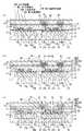
初めに、図1(a)に示すように、シリコン半導体基板10上に選択トランジスタ、図示の例ではトランジスタ構造20a,20b,20c,20dを形成する。ここで、トランジスタ構造20a,20b,20c,20dはCMOSトランジスタを構成し、20a,20bがNMOSトランジスタ、20c,20dがPMOSトランジスタとなる。 First, as shown in FIG. 1A, select transistors, in the illustrated example,
詳細には、先ず、シリコン半導体基板10の表層に例えばSTI(Shallow Trench Isolation)法により素子分離構造11を形成し、素子活性領域を確定する。
次に、レジストマスク(不図示)を形成する。このレジストマスクは、PMOSトランジスタとなるトランジスタ構造20c,20dの素子活性領域(以下、P活性領域と言う)を覆い、NMOSトランジスタとなるトランジスタ構造20a,20bの形成領域(以下、N活性領域と言う)を露出させる開口を有するものである。
そして、このレジストマスクを用いて、N活性領域にP型不純物、ここではホウ素(B)を例えばドーズ量3.0×10¹³/cm2、加速エネルギー300keVの条件でイオン注入し、N活性領域にP型ウェル12aを形成する。レジストマスクは灰化処理等により除去する。Specifically, first, the
Next, a resist mask (not shown) is formed. This resist mask covers the element active regions (hereinafter referred to as P active regions) of the
Then, using this resist mask, a P-type impurity, here boron (B), is ion-implanted into the N active region under conditions of a dose amount of 3.0 × 10¹³ / cm2 and an acceleration energy of 300 keV, for example. A P-
次に、N活性領域を覆いP活性領域を露出させる開口を有するレジストマスク(不図示)を形成する。
そして、このレジストマスクを用いて、P活性領域にN型不純物、ここではリン(P)を例えばドーズ量3.0×10¹³/cm2、加速エネルギー600keVの条件でイオン注入し、P活性領域にN型ウェル12bを形成する。レジストマスクは灰化処理等により除去する。Next, a resist mask (not shown) having an opening that covers the N active region and exposes the P active region is formed.
Then, using this resist mask, an N-type impurity, here phosphorus (P), is ion-implanted into the P active region under conditions of a dose amount of 3.0 × 10¹³ / cm2 and an acceleration energy of 600 keV, for example. An N-
次に、P,N活性領域にそれぞれ熱酸化等により膜厚3.0nm程度の薄いゲート絶縁膜13を形成し、ゲート絶縁膜13上にCVD法により膜厚180nm程度の多結晶シリコン膜及び膜厚29nm程度の例えばシリコン窒化膜を堆積する。そして、シリコン窒化膜、多結晶シリコン膜、及びゲート絶縁膜13をリソグラフィー及びそれに続くドライエッチングにより電極形状に加工する。これにより、P,N活性領域においてゲート絶縁膜13上にゲート電極14がそれぞれパターン形成される。このとき同時に、各ゲート電極14上にはシリコン窒化膜からなるキャップ膜15がパターン形成される。 Next, a thin
次に、P活性領域を覆いN活性領域を露出させる開口を有するレジストマスク(不図示)を形成する。
そして、このレジストマスク及びキャップ膜15をマスクとして、N活性領域にN型不純物、ここではAsを例えばドーズ量5.0×10¹⁴/cm2、加速エネルギー10keVの条件でイオン注入し、いわゆるLDD領域16aを形成する。Next, a resist mask (not shown) having an opening that covers the P active region and exposes the N active region is formed.
Then, using this resist mask and
次に、全面に例えばシリコン酸化膜をCVD法により堆積し、このシリコン酸化膜をいわゆるエッチバックすることにより、N活性領域におけるゲート電極14及びキャップ膜15の側面のみにシリコン酸化膜を残してサイドウォール絶縁膜17を形成する。 Next, for example, a silicon oxide film is deposited on the entire surface by the CVD method, and this silicon oxide film is so-called etched back to leave the silicon oxide film only on the side surfaces of the
次に、レジストマスク、キャップ膜15及びサイドウォール絶縁膜17をマスクとして、N活性領域にN型不純物をイオン注入する。ここでは、PをLDD領域16aよりも不純物濃度が高くなる条件、例えばドーズ量5.0×10¹⁴/cm2、加速エネルギー13keVの条件でイオン注入する。これにより、LDD領域16aと重畳されるソース/ドレイン領域18aが形成される。以上により、NMOSトランジスタとなるトランジスタ構造20a,20bを完成させる。レジストマスクは灰化処理等により除去する。Next, N-type impurities are ion-implanted into the N active region using the resist mask,
次に、N活性領域を覆いP活性領域を露出させる開口を有するレジストマスク(不図示)を形成する。
そして、このレジストマスク及びキャップ膜15をマスクとして、P活性領域にP型不純物、ここではBを例えばドーズ量1.0 ×10¹³/cm2、加速エネルギー15keVの条件でイオン注入し、いわゆるLDD領域16bを形成する。Next, a resist mask (not shown) having an opening that covers the N active region and exposes the P active region is formed.
Then, using this resist mask and
次に、全面に例えばシリコン酸化膜をCVD法により堆積し、このシリコン酸化膜をいわゆるエッチバックすることにより、P活性領域におけるゲート電極14及びキャップ膜15の側面のみにシリコン酸化膜を残してサイドウォール絶縁膜17を形成する。 Next, for example, a silicon oxide film is deposited on the entire surface by the CVD method, and this silicon oxide film is so-called etched back, so that the silicon oxide film is left only on the side surfaces of the
次に、レジストマスク、キャップ膜15及びサイドウォール絶縁膜17をマスクとして、P活性領域にP型不純物をイオン注入する。ここでは、BをLDD領域16bよりも不純物濃度が高くなる条件、例えばドーズ量2.0 ×10¹³/cm2、加速エネルギー5keVの条件でイオン注入する。これにより、LDD領域16bと重畳されるソース/ドレイン領域18bが形成される。以上により、PMOSトランジスタとなるトランジスタ構造20c,20dを完成させる。レジストマスクは灰化処理等により除去する。Next, P-type impurities are ion-implanted into the P active region using the resist mask,
続いて、図1(b)に示すように、トランジスタ構造20a,20b,20c,20dの保護膜21及び第1の層間絶縁膜22を形成する。
詳細には、トランジスタ構造20a,20b,20c,20dを覆うように、保護膜21及び絶縁膜22を順次堆積する。ここで、保護膜21としては、シリコン酸化膜を材料とし、CVD法により膜厚20nm程度に堆積する。第1の層間絶縁膜22としては、例えばプラズマSiO膜(膜厚20nm程度)、プラズマSiN膜(膜厚80nm程度)及びプラズマTEOS膜(膜厚1000nm程度)を順次成膜した積層構造を形成する。積層後、化学機械研磨(CMP)により膜厚が700nm程度となるまで研磨する。Subsequently, as shown in FIG. 1B, a
Specifically, the
続いて、図1(c)に示すように、トランジスタ構造20a,20b,20c,20dのソース/ドレイン領域18a,18bと接続される各プラグ36を形成する。ここでは図示の便宜上、プラグ36としては、ソース/ドレイン領域18bに形成するもののみを示す。
先ず、トランジスタ構造20a,20b,20c,20dへの各ビア孔34を形成する。
詳細には、第1の層間絶縁膜22及び保護膜21をリソグラフィー及びそれに続くドライエッチングにより加工する。これにより、ソース/ドレイン領域18a及びソース/ドレイン領域18bの表面の一部を露出させるビア孔34が例えば直径0.25μm程度にそれぞれ形成される。Subsequently, as shown in FIG. 1C, each plug 36 connected to the source /
First, each via
Specifically, the first
次に、ビア孔34の各壁面を覆うように、スパッタ法により例えばTi膜(膜厚30nm程度)及びTiN膜(膜厚20nm程度)を順次堆積して、下地膜(グルー膜)35を形成する。そして、CVD法によりグルー膜35を介してビア孔34を埋め込むように、W,TiAlN,TiN,Ti,Al,Cu,Ru,SRO,Irを材料とした単一膜又は積層膜、ここではW膜を形成する。その後、CMPにより絶縁膜21をストッパーとしてW膜及びグルー膜35を研磨し、ビア孔34内をグルー膜35を介してWで埋め込むプラグ36を形成する。 Next, for example, a Ti film (film thickness of about 30 nm) and a TiN film (film thickness of about 20 nm) are sequentially deposited so as to cover each wall surface of the via
続いて、図2(a)に示すように、酸化防止膜37及びプラズマTEOS膜38を形成した後、プラグ36と接続される各プラグ42を形成する。
詳細には、先ず、プラグ36の酸化防止膜37を、CVD法等により例えばSiONを材料として膜厚100nm程度に形成する。
次に、プラズマCVD法により、膜厚130nm程度のプラズマTEOS膜38を形成する。Subsequently, as shown in FIG. 2A, after forming the
In detail, first, the
Next, a
次に、プラズマTEOS膜38及び酸化防止膜37をリソグラフィー及びそれに続くドライエッチングにより加工し、プラグ36の表面の一部を露出させるビア孔39を例えば直径0.25μm程度にそれぞれ形成する。
次に、ビア孔39の各壁面を覆うように、スパッタ法により例えばTiN膜を膜厚50nm程度に堆積して、下地膜(グルー膜)41を形成する。そして、CVD法によりグルー膜41を介してビア孔39を埋め込むように、W,TiAlN,TiN,Ti,Al,Cu,Ru,SRO,Irの単一膜又は積層膜、ここではW膜を形成する。その後、CMPによりプラズマTEOS膜38をストッパーとしてW膜及びグルー膜41を研磨し、ビア孔39内をグルー膜41を介してWで埋め込むプラグ42を形成する。Next, the
Next, a base film (glue film) 41 is formed by depositing, for example, a TiN film with a film thickness of about 50 nm by sputtering so as to cover each wall surface of the via
続いて、図2(b)に示すように、保護下地膜43、下部電極層44、強誘電体膜45、下層上部電極層46、及び上層上部電極層47をそれぞれ形成する。その後、上層上部電極層47上にハードマスク材料48を形成する。
詳細には、先ず、導電膜である保護下地膜43を、例えばスパッタ法により膜厚100nm程度に形成する。保護下地膜43により、強誘電体膜45の後述する酸素アニール処理に起因するプラグ42の異常酸化、及びプラグ42の形成時に当該プラグ42内に取り込まれた水素の強誘電体膜45への影響が共に抑制される。保護下地膜43の材料としては、TiAlNの単層、TiNとTiAlNとの積層構造等、ここではTiNとTiAlNとの積層構造とする。Subsequently, as shown in FIG. 2B, a
Specifically, first, the
次に、スパッタ法により、膜厚100nm程度に例えばIrを堆積し、下部電極層44を形成する。
次に、MOCVD法により、450℃〜650℃程度、ここでは550℃にて下部電極層44上に強誘電体である例えばPZTからなる強誘電体膜45を膜厚100nm程度に堆積する。この際、強誘電体膜45が成膜当初アモルファス状態にある場合はRTA処理を施して当該強誘電体膜45を結晶化する。一方、既に強誘電体45が結晶化している場合は必ずしもRTA処理を必要としない。Next, Ir, for example, is deposited to a thickness of about 100 nm by sputtering to form the lower electrode layer 44.
Next, a
ここで、強誘電体膜45は、大容量及び低電圧動作化を実現すべく比較的薄い膜厚、例えば50nm程度〜200nm程度とすることが好ましい。ここで、強誘電体膜45の膜厚が50nmより薄い場合、(リーク電流増加)の点で問題がある。一方、200nm程度より厚い場合、大容量及び低電圧動作化を十分に得ることが困難となる。従って、上記の範囲内の膜厚に強誘電体膜45を形成することが好適である。本実施形態では、当該範囲内の値として100nm程度となるように強誘電体膜45を形成する。
また、強誘電体膜45の強誘電体材料としては、PZTの代わりにSBT,BIT,BFOから選ばれた少なくとも1種を用いるようにしても良い。Here, it is preferable that the
Further, as the ferroelectric material of the
次に、反応性スパッタ法により、強誘電体膜45上に例えば導電性酸化物であるIrO2を膜厚100nm程度に堆積し、下層上部電極層46を形成する。
そして、スパッタ法により、下層上部電極層46上に例えばIrを膜厚100nm程度に堆積し、上層上部電極層47を形成する。Next, for example, IrO2 , which is a conductive oxide, is deposited on the
Then, for example, Ir is deposited to a thickness of about 100 nm on the lower
なお、下部電極層44、下層上部電極層46、及び上層上部電極層47の材料としては、上記の場合も含め、以下のものを用いても良い。即ち、Ir,IrOx(典型的にはx=2),Pt,SRO,LNO,LSCO,Ru,RuO2、SrRuO3等から選ばれた少なくとも1種がそれぞれ用いられる。In addition, as a material of the lower electrode layer 44, the lower layer
次に、上層上部電極層47上に、CVD法等により例えばTEOS膜を膜厚600nm程度に堆積し、ハードマスク材料48を形成する。 Next, a TEOS film, for example, is deposited to a thickness of about 600 nm on the upper
続いて、図2(c)に示すように、強誘電体メモリキャパシタである第1のキャパシタ30を形成する。
詳細には、ハードマスク材料48を用い、例えば400℃にて、上層上部電極層47、下層上部電極層46、強誘電体膜45、下部電極層44、及び保護下地膜43を一括エッチングする。そして、ハードマスク材料48をウェットエッチング等で除去する。これにより、第1のキャパシタ30が完成する。第1のキャパシタ30は、例えばP活性領域にプラグ42と保護下地膜43を介し、下部電極層44からなる下部電極51と、下層上部電極層46及び上層上部電極層47の積層構造である上部電極52とで強誘電体膜45を挟持してなるものである。Subsequently, as shown in FIG. 2C, a
Specifically, using the hard mask material 48, the upper
続いて、図3(a)に示すように、第1のキャパシタ30を覆う第2の層間絶縁膜49を形成する。
詳細には、先ず、第1のキャパシタ30を覆うようにプラズマTEOS膜38上に金属酸化膜、例えばALD(Atomic Layer Deposition)−ALO膜を膜厚2nm程度に堆積する。そして、処理温度600℃、酸素雰囲気で40分間、第1のキャパシタ30のダメージを回復するために、酸素アニールを実行する。その後、再びALD−ALO膜を膜厚38nm程度に堆積する。以上により、第1のキャパシタ30を覆う第1の保護膜49aが形成される。Subsequently, as shown in FIG. 3A, a second
Specifically, first, a metal oxide film, for example, an ALD (Atomic Layer Deposition) -ALO film is deposited on the
次に、例えば高密度プラズマ(HDP)CVD法により、第1の保護膜49aを介して第1のキャパシタ30を覆うようにシリコン酸化膜を膜厚1400nm程度に堆積した後、CMPによりシリコン酸化膜の表面を平坦化して、下部絶縁膜49bを形成する。また、シリコン酸化膜は平行平板プラズマCVD法で成膜してもよい。
次に、下部絶縁膜49bの脱水を目的として、例えばN2Oプラズマアニール処理を施す。その後、下部絶縁膜49b上に金属酸化膜、例えばALD−ALO膜を膜厚30nm程度に堆積し、第1のキャパシタ30の第2の保護膜49bを形成する。
次に、プラズマCVD法により、第2の保護膜49b上にシリコン酸化膜を膜厚300nm程度に堆積し、上部絶縁膜49cを形成する。Next, a silicon oxide film is deposited to a thickness of about 1400 nm so as to cover the
Next, for example, N2 O plasma annealing is performed for the purpose of dehydrating the lower insulating
Next, a silicon oxide film is deposited to a thickness of about 300 nm on the second
以上により、第1の保護膜49a、下部絶縁膜49b、第2の保護膜49c及び上部絶縁膜49dが順次堆積されてなる第2の層間絶縁膜49が形成される。
第2の層間絶縁膜49では、第1の保護膜49a及び第2の保護膜49cにより、例えば後工程により形成されるシリコン酸化膜等からの水分・水素の強誘電体膜45への浸入が抑止され、強誘電体膜45へのダメージが防止される。As described above, the second
In the second
続いて、図3(b)に示すように、ビア孔53を形成する。
詳細には、リソグラフィー及びドライエッチングにより、第1のキャパシタ30の上部電極52の上方に整合した部位で第2の層間絶縁膜49を加工し、上部電極52の表面の一部を露出させるビア孔53を形成する。Subsequently, as shown in FIG. 3B, a via
Specifically, the second
その後、第1のキャパシタ30のエッチング時に受けたダメージを回復するために、酸素アニール処理を実行する。ここでは例えば、処理温度500℃、酸素雰囲気で60分間のアニール処理を実行する。本実施形態では、第1のキャパシタ30とプラグ42との間に保護下地膜43が設けられているため、この酸素アニール処理を実行してもプラグ42の異常酸化が防止される。それと共に、保護下地膜43によりプラグ42の形成時に当該プラグ42内に取り込まれた水素の発生が抑止される。 Thereafter, in order to recover the damage received during the etching of the
続いて、図3(c)に示すように、ビア孔54を形成する。
詳細には、リソグラフィー及びドライエッチングにより、プラグ36の上方に整合した部位で第2の層間絶縁膜49、プラズマTEOS膜38、及び酸化防止膜37を加工し、プラグ36の表面の少なくとも一部を露出させるビア孔54を形成する。Subsequently, as shown in FIG. 3C, a via
Specifically, the second
続いて、図4(a)に示すように、第1のキャパシタ30の上部電極52と接続される各プラグ57と、プラグ36と接続される各プラグ58とを形成する。
詳細には、ビア孔53,54の各壁面を覆うように、スパッタ法により例えばTiN膜を膜厚125nm程度に堆積して、下地膜(グルー膜)55,56を形成する。そして、CVD法によりグルー膜55,56を介してビア孔53,54を埋め込むように、W,TiAlN,TiN,Ti,Al,Cu,Ru,SRO,Irの単一膜又は積層膜、ここではW膜を形成する。その後、CMPにより第1の層間絶縁膜49をストッパーとしてW膜及びグルー膜55,56を研磨し、ビア孔53,54内をグルー膜55,56を介してWで埋め込むプラグ57,58をそれぞれ形成する。Subsequently, as shown in FIG. 4A, each plug 57 connected to the upper electrode 52 of the
Specifically, for example, a TiN film is deposited to a thickness of about 125 nm by sputtering so as to cover the wall surfaces of the via holes 53 and 54 to form base films (glue films) 55 and 56. A single film or a laminated film of W, TiAlN, TiN, Ti, Al, Cu, Ru, SRO, and Ir, so as to fill the via holes 53 and 54 via the
続いて、図4(b)に示すように、酸化防止膜59及びプラズマTEOS膜61を形成する。
詳細には、先ず、プラグ57,58の酸化防止膜59を、CVD法等により例えばSiONを材料として膜厚100nm程度に形成する。
次に、プラズマCVD法により、膜厚130nm程度のプラズマTEOS膜61を形成する。Subsequently, as shown in FIG. 4B, an
Specifically, first, the
Next, a
続いて、図4(c)に示すように、結晶性改善膜62、下部電極層63、強誘電体膜64、及び上部電極層65をそれぞれ形成する。
詳細には、先ず、プラズマTEOS膜61上に、後述の強誘電体キャパシタ60の下部電極及び強誘電体膜の結晶性を改善するための結晶性改善膜62を形成する。Subsequently, as shown in FIG. 4C, a
More specifically, first, a
次に、スパッタ法により、膜厚150nm程度に例えばPtを堆積し、下部電極層63を形成する。
次に、スパッタ法により、20℃〜100℃程度、ここでは50℃にて下部電極層63上に強誘電体である例えばPZTからなる強誘電体膜64を膜厚150nm程度に堆積する。この際、強誘電体膜64が成膜当初アモルファス状態にあるので、RTA処理を施して当該強誘電体膜64を結晶化する。例えば、500℃程度の温度で処理をする。或いは、炉アニールにより結晶化させても良い。その際、例えば400℃程度の温度で処理をする。Next, for example, Pt is deposited to a thickness of about 150 nm by sputtering to form the
Next, a
ここで、強誘電体膜64は、比較的大きな容量を確保しつつも十分な耐圧特性を得るべく、比較的厚い膜厚、例えば100nm程度〜300nm程度とすることが好ましい。ここで、強誘電体膜64の膜厚が100nmより薄い場合、十分な耐圧特性を得ることが困難となる。一方、500nm程度より厚い場合、十分な容量が確保できないという問題がある。従って、上記の範囲内の膜厚に強誘電体膜64を形成することが好適である。本実施形態では、当該範囲内の値として、第1のキャパシタ30の強誘電体膜45よりも厚い150nm程度となるように強誘電体膜45を形成する。
また、強誘電体膜64の強誘電体材料としては、PZTの代わりにSBT,BIT,BFOから選ばれた少なくとも1種を用いるようにしても良い。Here, it is preferable that the
Further, as the ferroelectric material of the
次に、反応性スパッタ法により、強誘電体膜64上に例えば導電性酸化物であるIrO2を膜厚250nm程度に堆積し、上部電極層65を形成する。
なお、下部電極層63及び上部電極層65の材料としては、上記の場合も含め、Ir,IrOx(典型的にはx=2),Pt,SRO,LNO,LSCO,Ru,RuO2、SrRuO3等から選ばれた少なくとも1種がそれぞれ用いられる。Next, IrO2 , which is a conductive oxide, for example, is deposited on the
The materials of the
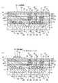
続いて、図5―1(a)に示すように、上部電極67をパターン形成する。
詳細には、上部電極層65をリソグラフィー及びそれに続くドライエッチングにより複数の電極形状に加工して、上部電極67をパターン形成する。
ここで、上部電極67は、第1のキャパシタ30の上部電極52よりも平面視における占有面積が大きく形成されている。Subsequently, as shown in FIG. 5A, the
Specifically, the upper electrode layer 65 is processed into a plurality of electrode shapes by lithography and subsequent dry etching, and the
Here, the
続いて、図5―1(b)に示すように、強誘電体膜64及び下部電極層63を加工して、第2のキャパシタ50を形成する。第2のキャパシタ50は、メモリキャパシタ以外の強誘電体キャパシタ、例えば平滑キャパシタ又は電源キャパシタである。本実施形態では、第2のキャパシタ50として、比較的大きな占有面積を有し比較的容易に形成可能なプレーナ型を採用する。
詳細には、先ず、強誘電体膜64を上部電極67に整合させて、当該上部電極67よりも若干大きい(或いは略同等)サイズとなるように、リソグラフィー及びそれに続くドライエッチングにより加工する。Subsequently, as shown in FIG. 5B, the
Specifically, first, the
次に、下部電極層63を、加工された強誘電体膜64に整合させて、当該強誘電体膜64よりも適宜大きいサイズとなるように、リソグラフィー及びそれに続くドライエッチングにより加工し、下部電極66をパターン形成する。これにより、下部電極66上に強誘電体膜64、上部電極66が順次積層され、強誘電体膜64を介して下部電極66と上部電極67とが容量結合する第2のキャパシタ50を完成させる。
その後、強誘電体膜64のエッチング時に受けたダメージを回復するために、酸素アニール処理を実行する。Next, the
Thereafter, in order to recover the damage received during the etching of the
続いて、図5―2に示すように、第2のキャパシタ50を覆う第3の層間絶縁膜68を形成する。
詳細には、先ず、第2のキャパシタ50を覆うように、プラズマTEOS膜61上に例えばALD(Atomic Layer Deposition)−ALO膜を膜厚20nm程度に堆積する。これにより、第2のキャパシタ50を覆う第3の保護膜68aが形成される。この第3の保護膜68aにより、例えば後工程により形成されるシリコン酸化膜等からの水分・水素の強誘電体膜64への浸入が抑止され、強誘電体膜64へのダメージが防止される。その後、処理温度650℃、酸素雰囲気で60分間、第2のキャパシタ50のダメージを回復するために、酸素アニールを実行する。Subsequently, as shown in FIG. 5B, a third
Specifically, first, for example, an ALD (Atomic Layer Deposition) -ALO film is deposited to a thickness of about 20 nm on the
次に、例えば高密度プラズマ(HDP)CVD法により、第3の保護膜68aを介して第2のキャパシタ50を覆うようにシリコン酸化膜を膜厚1500nm程度に堆積した後、CMPによりシリコン酸化膜の膜厚が1000nm程度となるまでその表面を平坦化する。これにより、絶縁膜68bが形成される。また、シリコン酸化膜は平行平板プラズマCVD法で成膜してもよい。その後、絶縁膜68bの脱水を目的として、例えばN2Oプラズマアニール処理を施す。
以上により、第3の保護膜68a及び絶縁膜68bが順次堆積されてなる第3の層間絶縁膜68が形成される。Next, a silicon oxide film is deposited to a thickness of about 1500 nm so as to cover the
Thus, the third
続いて、図6―1(a)に示すように、ビア孔69a,69bを同一工程で形成する。
詳細には、リソグラフィー及びドライエッチングにより、第2のキャパシタ50の上部電極67の上方に整合した部位及び下部電極66の上方に整合した部位で第3の層間絶縁膜68をそれぞれ加工する。Subsequently, as shown in FIG. 6A, via
Specifically, the third
上記の加工により、上部電極67の表面の一部を露出させるビア孔69a、下部電極66の表面の一部を露出させるビア孔69bが、同一工程で形成される。
その後、第2のキャパシタ50のエッチング時に受けたダメージを回復するために、酸素アニール処理を実行する。ここでは例えば、処理温度500℃、酸素雰囲気で60分間処理する。
続いて、図6―1(a)に示すように、ビア孔69c,69dを同一工程で形成する。
詳細には、リソグラフィー及びドライエッチングにより、プラグ57の上方に整合した部位及びプラグ58の上方に整合した部位で第3の層間絶縁膜68、プラズマTEOS膜61及び酸化防止膜59をそれぞれ加工する。
上記の加工により、プラグ57の表面の一部を露出させるビア孔69c、及びプラグ58の表面の一部を露出させるビア孔69dが、同一工程で形成される。By the above processing, a via
Thereafter, an oxygen annealing process is performed to recover the damage received during the etching of the
Subsequently, as shown in FIG. 6A, via
Specifically, the third
By the above processing, a via
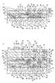
続いて、図6―1(b)に示すように、上部電極67と接続されるプラグ72a、下部電極66と接続されるプラグ72b、プラグ57と接続されるプラグ72c、及びプラグ58と接続されるプラグ72dを形成する。
詳細には、ビア孔69a,69b,69c,69dの各壁面を覆うように、スパッタ法により例えばTiN膜を膜厚125nm程度に堆積して、下地膜(グルー膜)71a,71b,71c,71dを形成する。そして、CVD法によりグルー膜71a,71b,71c,71dを介してビア孔69a,69b,69c,69dを埋め込むように、W,TiAlN,TiN,Ti,Al,Cu,Ru,SRO,Irの単一膜又は積層膜、ここではW膜を形成する。その後、CMPにより第3の層間絶縁膜68をストッパーとしてW膜及びグルー膜71a,71b,71c,71dを研磨する。これにより、ビア孔69a,69b,69c,69d内をグルー膜71a,71b,71c,71dを介してWで埋め込むプラグ72a,72b,72c,72dがそれぞれ形成される。Subsequently, as shown in FIG. 6B, the
Specifically, for example, a TiN film is deposited to a thickness of about 125 nm by a sputtering method so as to cover the wall surfaces of the via
続いて、図6―2に示すように、プラグ72a,72b,72c,72dと接続される第1の配線76をそれぞれ形成する。
詳細には、先ず、スパッタ法により、第3の層間絶縁膜68上に例えばTi(膜厚60nm程度)及びTiN(膜厚30nm程度)を順次堆積してバリアメタル膜73を形成する。
次に、スパッタ法により、バリアメタル膜73上に例えばAl−Cu合金を膜厚360nm程度に堆積して配線層74を形成する。この配線層構造は、同一ルールのFeRAM以外のロジック回路と同じ構造となっているため、配線の加工や信頼性に問題はない。Subsequently, as shown in FIG. 6B,
Specifically, first, a
Next, for example, an Al—Cu alloy is deposited on the
次に、スパッタ法により、配線層74上に例えばTi(膜厚5nm程度)及びTiN(膜厚70nm程度)を順次堆積してバリアメタル膜75を形成する。
そして、バリアメタル膜75、配線層74、及びバリアメタル膜73をリソグラフィー及びドライエッチングにより配線形状に加工する。この加工により、プラグ72a,72b,72c,72dと接続される第1の配線76がそれぞれ形成される。Next, for example, Ti (film thickness of about 5 nm) and TiN (film thickness of about 70 nm) are sequentially deposited on the
Then, the
続いて、図7―1に示すように、第1の配線76を覆う層間絶縁膜77及びプラグ81を順次形成する。
詳細には、先ず、CVD法等により、第1の配線76を覆うように第3の層間絶縁膜68上に例えばシリコン酸化膜を形成し、CMPによりシリコン酸化膜の表面を平坦化して、層間絶縁膜77を形成する。Subsequently, as shown in FIG. 7A, an
Specifically, first, for example, a silicon oxide film is formed on the third
次に、リソグラフィー及びドライエッチングにより、第1の配線76の上方に整合した部位で層間絶縁膜77を加工し、第1の配線76の表面の一部を露出させるビア孔78を形成する。
次に、ビア孔78の各壁面を覆うように、スパッタ法により例えばTiN膜を膜厚125nm程度に堆積して、下地膜(グルー膜)79を形成する。そして、CVD法によりグルー膜79を介してビア孔78を埋め込むように、W,TiAlN,TiN,Ti,Al,Cu,Ru,SRO,Irの単一膜又は積層膜、ここではW膜を形成する。その後、CMPにより層間絶縁膜77をストッパーとしてW膜及びグルー膜79を研磨し、ビア孔78内をグルー膜79を介してWで埋め込むプラグ81をそれぞれ形成する。
第1の配線76、層間絶縁膜77及びプラグ81により、第1の配線構造90aが構成される。Next, the
Next, a base film (glue film) 79 is formed by depositing, for example, a TiN film with a film thickness of about 125 nm by sputtering so as to cover each wall surface of the via
A first wiring structure 90 a is configured by the
続いて、図7―2に示すように、本実施形態によるスタック型のFeRAMを完成させる。
詳細には、先ず、第1の配線構造90aと同様に、第1の配線構造90a上に複数の配線構造、ここでは第2、第3及び第4の配線構造90b,90c,90dを形成する。
ここで、第2の配線構造90bは、プラグ81と接続される第2の配線82、第2の配線82を覆う層間絶縁膜83、及び第2の配線82と接続されるプラグ84を有して構成される。
第3の配線構造90cは、プラグ84と接続される第3の配線85、第3の配線85を覆う層間絶縁膜86、及び第3の配線85と接続されるプラグ87を有して構成される。
第4の配線構造90dは、プラグ87と接続される第4の配線88、第4の配線88を覆う層間絶縁膜89、及び第4の配線88と接続されるプラグ91を有して構成される。Subsequently, as shown in FIG. 7B, the stack type FeRAM according to the present embodiment is completed.
Specifically, first, similarly to the first wiring structure 90a, a plurality of wiring structures, here, the second, third and
Here, the
The
The
そして、第5の配線構造90eを形成する。
詳細には、先ず、スパッタ法により、第4の配線構造90d上にAl−Cu合金を堆積し、これをリソグラフィー及びドライエッチングにより加工して、プラグ91と接続される第5の配線92及びパッド93を形成する。パッド93は、プラグ91、第4の配線88、プラグ87、第3の配線85、プラグ84、第2の配線82、及びプラグ81を順次介して、第1の配線76と電気的に接続された構成を採る。
本実施形態では、第5の配線92及びパッド93から第5の配線構造90eが構成される。Then, a
More specifically, first, an Al—Cu alloy is deposited on the
In the present embodiment, a
次に、第5の配線構造90eを覆うように、第4の配線構造90d上に、プラズマCVD法により高密度プラズマを用いてHDP−USG膜を膜厚720nm程度に堆積し、第1のカバー膜94を形成する。
次に、第1のカバー膜94上に、CVD法によりSiN膜を膜厚500nm程度に堆積し、第2のカバー膜95を形成する。Next, an HDP-USG film is deposited on the
Next, a SiN film is deposited to a thickness of about 500 nm on the
次に、第2のカバー膜95及び第1のカバー膜94をリソグラフィー及びドライエッチングにより加工し、パッド93の表面の一部を露出させる開口部96を形成する。
しかる後、全面にポリイミド膜97を成膜し、ポリイミド膜97の開口部96に相当する部分をリソグラフィー及びドライエッチングにより加工して、パッド93の表面の一部を露出させる開口部98を形成する。
以上により、本実施形態によるスタック型のFeRAMを完成させる。Next, the
Thereafter, a
Thus, the stack type FeRAM according to the present embodiment is completed.
以上説明したように、本実施形態では、メモリセルにおけるメモリキャパシタである第1のキャパシタ30と、メモリキャパシタ以外の第2のキャパシタ50とを混載してなるFeRAMを対象とする。本実施形態によれば、大容量化及び微細化、低電圧化という第1のキャパシタ30に対する要請と、大容量化及び高耐圧化という第2のキャパシタ50に対する要請という異なる要求を共に十分に満たす信頼性の高いFeRAMが実現する。 As described above, the present embodiment is directed to the FeRAM in which the
(変形例)
ここで、第1の実施形態の変形例について説明する。本例では、第1の実施形態と同様に第1のキャパシタ30及び第2のキャパシタ50を備えたスタック型のFeRAMを対象とするが、第2のキャパシタ50の形成位置が異なる点で第1の実施形態と相違する。なお、第1の実施形態で説明した構成部材等と同様のものについては同符号を付す。
図8〜図9―2は、第1の実施形態の変形例によるスタック型のFeRAMの構成をその主要工程と共に示す概略断面図である。(Modification)
Here, a modification of the first embodiment will be described. In this example, the stack type FeRAM including the
FIGS. 8 to 9-2 are schematic cross-sectional views showing the structure of the stack type FeRAM according to the modification of the first embodiment together with its main steps.
本例では、先ず、第1の実施形態と同様に、図1(a)〜図4(a)の各工程を経る。
続いて、図8(a)に示すように、プラグ57,58と接続される第1の配線76をそれぞれ形成する。
詳細には、先ず、スパッタ法により、第3の層間絶縁膜68上に例えばTi(膜厚60nm程度)及びTiN(膜厚30nm程度)を順次堆積してバリアメタル膜73を形成する。
次に、スパッタ法により、バリアメタル膜73上に例えばAl−Cu合金を膜厚360nm程度に堆積して配線層74を形成する。この配線層構造は、同一ルールのFeRAM以外のロジック回路と同じ構造となっているため、配線の加工や信頼性に問題はない。In this example, first, similarly to the first embodiment, the respective steps of FIG. 1A to FIG. 4A are performed.
Subsequently, as shown in FIG. 8A,
Specifically, first, a
Next, for example, an Al—Cu alloy is deposited on the
次に、スパッタ法により、配線層74上に例えばTi(膜厚5nm程度)及びTiN(膜厚70nm程度)を順次堆積してバリアメタル膜75を形成する。
そして、バリアメタル膜75、配線層74、及びバリアメタル膜73をリソグラフィー及びドライエッチングにより配線形状に加工する。この加工により、プラグ57,58と接続される第1の配線76がそれぞれ形成される。Next, for example, Ti (film thickness of about 5 nm) and TiN (film thickness of about 70 nm) are sequentially deposited on the
Then, the
続いて、第1の実施形態と同様に、図7(a)による第1の配線構造90aの形成、図7(b)による第2〜第4の配線構造90b,90c,90dの形成を実行する。 Subsequently, as in the first embodiment, the first wiring structure 90a is formed according to FIG. 7A, and the second to
続いて、図8(b)に示すように、第1のキャパシタ30が形成された第2の層間絶縁膜49から2層以上高い層位置、本例では第4の配線構造90d上にメモリキャパシタ以外の強誘電体キャパシタである第2のキャパシタ50を形成する。
ここでは、第1の実施形態と同様に、図4(c)、図5(a)、図5(b)の各工程を実行して、第4の配線構造90d上に第2のキャパシタ50を形成する。但し、スパッタ法により強誘電体膜64を堆積する際に、結晶化アニールの処理温度をRTA法であれば600℃以下、ここでは例えば500℃、FA法(炉アニール)であれば430℃以下、ここでは例えば400℃とする。第1〜第4の配線構造90a,90b,90c,90dの第1〜第4の配線76,82,85,88はAl−Cu合金を材料とするため、450℃〜650℃程度の処理温度により溶解する虞がある。一方、強誘電体膜64の材料であるPZTは成膜温度が450℃より低温であると配向性の十分な制御が困難となる。しかしながら、第2のキャパシタ50は、平滑キャパシタや電源キャパシタ等のメモリキャパシタ以外の強誘電体キャパシタであるため、強誘電体膜における配向性制御にメモリキャパシタほどの精度は要求されない。従って、強誘電体膜64は、400℃程度の成膜温度でも十分にその機能を果たすことができる。
また、上記と同様の理由により、強誘電体膜64の各エッチング時に受けたダメージを回復するために行う酸素アニール処理でも、処理温度を430℃以下、ここでは例えば400℃とする。Subsequently, as shown in FIG. 8B, a memory capacitor is formed on a layer position that is two or more layers higher than the second
Here, as in the first embodiment, the steps of FIG. 4C, FIG. 5A, and FIG. 5B are executed, and the
For the same reason as described above, the processing temperature is set to 430 ° C. or lower, for example, 400 ° C. in the oxygen annealing process performed to recover the damage received during the etching of the
続いて、図9―1に示すように、第2のキャパシタ50を覆う第3の層間絶縁膜68を形成した後、上部電極67と接続されるプラグ72a、下部電極66と接続されるプラグ72bを形成する。
先ず、第1の実施形態と同様に、図5(c)の工程を実行して、第4の配線構造90d上に第2のキャパシタ50を覆うように第3の層間絶縁膜68を形成する。Subsequently, as shown in FIG. 9A, after forming a third
First, as in the first embodiment, the third
次に、ビア孔69a,69bを同一工程で形成する。
詳細には、リソグラフィー及びドライエッチングにより、第2のキャパシタ50の上部電極67の上方に整合した部位及び下部電極66の上方に整合した部位で第3の層間絶縁膜68をそれぞれ加工する。Next, via
Specifically, the third
上記の加工により、上部電極67の表面の一部を露出させるビア孔69a、下部電極66の表面の一部を露出させるビア孔69bが、同一工程で形成される。
その後、第2のキャパシタ50のエッチング時に受けたダメージを回復するために、酸素アニール処理を実行する。ここでも上記と同様の理由により、処理温度を430℃以下、ここでは例えば400℃とする。By the above processing, a via
Thereafter, an oxygen annealing process is performed to recover the damage received during the etching of the
続いて、図9―1に示すように、プラグ91と接続されるプラグ99を形成する。
先ず、ビア孔69a,69b,99aを同一工程で形成する。
詳細には、リソグラフィー及びドライエッチングにより、プラグ91の上方に整合した部位で第3の層間絶縁膜68を加工する。
上記の加工により、プラグ91の表面の一部を露出させるビア孔99aが形成される。Subsequently, as shown in FIG. 9A, a
First, via
Specifically, the third
By the above processing, a via
次に、ビア孔69a,69b,99aの各壁面を覆うように、スパッタ法により例えばTiN膜を膜厚125nm程度に堆積して、下地膜(グルー膜)71a,71b,99beを形成する。そして、CVD法によりグルー膜71a,71b,99bを介してビア孔69a,69b,99aを埋め込むように、W,TiAlN,TiN,Ti,Al,Cu,Ru,SRO,Irの単一膜又は積層膜、ここではW膜を形成する。その後、CMPにより第3の層間絶縁膜68をストッパーとしてW膜及びグルー膜71a,71b,99bを研磨し、ビア孔69a,69b,99a内をグルー膜71a,71b,99bを介してWで埋め込むプラグ72a,72b,99をそれぞれ形成する。 Next, a TiN film, for example, is deposited to a thickness of about 125 nm by a sputtering method so as to cover the wall surfaces of the via
続いて、図9―2に示すように、第3の層間絶縁膜68上に第1の実施形態と同様に、第5の配線構造90eを形成した後、第1のカバー膜94及び第2のカバー膜95の形成、開口部96の形成、ポリイミド膜97の形成、及び開口部98の形成を経て、スタック型のFeRAMを完成させる。 Subsequently, as shown in FIG. 9B, after the
以上説明したように、本例では、メモリセルにおけるメモリキャパシタである第1のキャパシタ30と、メモリキャパシタ以外の第2のキャパシタ50とを混載してなるFeRAMを対象とする。本例によれば、大容量化及び微細化、低電圧化という第1のキャパシタ30に対する要請と、大容量化及び高耐圧化という第2のキャパシタ50に対する要請という異なる要求を共に十分に満たす信頼性の高いFeRAMが実現する。 As described above, in this example, the target is an FeRAM in which the
更に本例では、第2のキャパシタ50の形成される層位置に殆ど制約がなく、所定の上層位置に適宜形成することが可能である。従って、半導体装置としての設計の自由度が向上し、強誘電体容量として平滑キャパシタや電源キャパシタを装置構成に応じて適宜所望の層位置に形成することができる。 Furthermore, in this example, there is almost no restriction on the layer position where the
(第2の実施形態)
第2の実施形態では、プレーナ型のFeRAMの構成及びその製造方法について説明する。
図10〜図15―2は、第2の実施形態によるプレーナ型のFeRAMの構成をその製造方法と共に工程順に示す概略断面図である。(Second Embodiment)
In the second embodiment, a configuration of a planar type FeRAM and a manufacturing method thereof will be described.
10 to 15-2 are schematic cross-sectional views showing the structure of the planar type FeRAM according to the second embodiment in the order of steps together with the manufacturing method thereof.
先ず、図10(a)に示すように、シリコン半導体基板110上に選択トランジスタとして機能するトランジスタ構造120a,120bを形成する。
詳細には、シリコン半導体基板110の表層に例えばSTI法により素子分離構造111を形成し、素子活性領域を確定する。
次に、素子活性領域に不純物、ここではBを例えばドーズ量3.0×10¹³/cm2、加速エネルギー300keVの条件でイオン注入し、ウェル112を形成する。First, as shown in FIG. 10A, transistor structures 120 a and 120 b that function as selection transistors are formed on a
Specifically, the
Next, an impurity, here B, is ion-implanted into the element active region under conditions of a dose amount of 3.0 × 10¹³ / cm2 and an acceleration energy of 300 keV to form the
次に、素子活性領域に熱酸化等により膜厚3.0nm程度の薄いゲート絶縁膜113を形成し、ゲート絶縁膜113上にCVD法により膜厚180nm程度の多結晶シリコン膜及び膜厚29nm程度の例えばシリコン窒化膜を堆積する。そして、シリコン窒化膜、多結晶シリコン膜、及びゲート絶縁膜113をリソグラフィー及びそれに続くドライエッチングにより電極形状に加工する。これにより、ゲート絶縁膜113上にゲート電極114がパターン形成される。このとき同時に、ゲート電極114上にはシリコン窒化膜からなるキャップ膜115がパターン形成される。 Next, a thin
次に、キャップ膜115をマスクとして素子活性領域に不純物、ここではAsを例えばドーズ量5.0×10¹⁴/cm2、加速エネルギー10keVの条件でイオン注入し、いわゆるLDD領域116を形成する。Next, using the
次に、全面に例えばシリコン酸化膜をCVD法により堆積し、このシリコン酸化膜をいわゆるエッチバックすることにより、ゲート電極114及びキャップ膜115の側面のみにシリコン酸化膜を残してサイドウォール絶縁膜117を形成する。 Next, for example, a silicon oxide film is deposited on the entire surface by a CVD method, and this silicon oxide film is so-called etched back to leave the silicon oxide film only on the side surfaces of the
次に、キャップ膜115及びサイドウォール絶縁膜117をマスクとして素子活性領域に不純物、ここではPをLDD領域116よりも不純物濃度が高くなる条件、例えばドーズ量5.0×10¹⁴/cm2、加速エネルギー13keVの条件でイオン注入する。これにより、LDD領域116と重畳されるソース/ドレイン領域118を形成して、トランジスタ構造120a,120bを完成させる。Next, using the
続いて、図10(b)に示すように、トランジスタ構造120a,120bの保護膜121及び第1の層間絶縁膜122を形成する。
詳細には、トランジスタ構造120a,120bを覆うように、保護膜121及び絶縁膜122を順次堆積する。ここで、保護膜121としては、シリコン酸化膜を材料とし、CVD法により膜厚20nm程度に堆積する。第1の層間絶縁膜122としては、例えばプラズマSiO膜(膜厚20nm程度)、プラズマSiN膜(膜厚80nm程度)及びプラズマTEOS膜(膜厚1000nm程度)を順次成膜した積層構造を形成する。積層後、CMPにより膜厚が700nm程度となるまで研磨する。Subsequently, as shown in FIG. 10B, a
Specifically, a
続いて、図10(c)に示すように、後述する第1のキャパシタ130の下部電極の配向性向上膜123を形成する。
詳細には、第1の層間絶縁膜122上に例えばシリコン酸化膜を堆積し、配向性向上膜123を形成する。Subsequently, as shown in FIG. 10C, an
Specifically, for example, a silicon oxide film is deposited on the first
続いて、図11(a)に示すように、下部電極層124、強誘電体膜125及び上部電極層126を順次形成する。
詳細には、先ずスパッタ法により例えば膜厚が20nm程度のTi膜及び膜厚が150nm程度のPt膜を順次堆積させ、Ti膜及びPt膜の積層構造に下部電極層124を形成する。Subsequently, as shown in FIG. 11A, a
Specifically, first, for example, a Ti film having a film thickness of about 20 nm and a Pt film having a film thickness of about 150 nm are sequentially deposited by sputtering to form the
次に、スパッタ法により、20℃〜100℃程度、ここでは50℃にて下部電極層124上に強誘電体である例えばPZTからなる強誘電体膜125を膜厚200nm程度に堆積する。この際、強誘電体膜125が成膜当初アモルファス状態にあるので、RTA処理を施して当該強誘電体膜125を結晶化する。例えば、500℃程度の温度で処理をする。あるいは、炉アニールにより結晶化させてもよい。その際、例えば400℃程度の温度で処理をする。 Next, a
ここで、強誘電体膜125は、大容量及び低電圧動作化を実現すべく比較的薄い膜厚、例えば90nm程度〜200nm程度とすることが好ましい。ここで、強誘電体膜125の膜厚が90nmより薄い場合、リーク電流が増加するという問題がある。一方、200nm程度より厚い場合、大容量及び低電圧動作化を十分に得ることが困難となる。従って、上記の範囲内の膜厚に強誘電体膜125を形成することが好適である。本実施形態では、当該範囲内の値として100nm程度となるように強誘電体膜125を形成する。
また、強誘電体膜125の強誘電体材料としては、PZTの代わりにSBT,BIT,BFOから選ばれた少なくとも1種を用いるようにしても良い。Here, it is preferable that the
Further, as the ferroelectric material of the
次に、反応性スパッタ法により、強誘電体膜125上に例えば導電性酸化物であるIrO2を材料とする上部電極層126を膜厚200nm程度に堆積する。なお、上部電極層126の材料として、IrO2の代わりにIr、Ru、RuO2、SrRuO3、その他の導電性酸化物やこれらの積層構造としても良い。Next, an upper electrode layer 126 made of, for example, IrO2 that is a conductive oxide is deposited on the
続いて、図11(b)に示すように、上部電極132をパターン形成する。
詳細には、上部電極層126をリソグラフィー及びそれに続くドライエッチングにより複数の電極形状に加工して、上部電極132をパターン形成する。Subsequently, as shown in FIG. 11B, the
Specifically, the upper electrode layer 126 is processed into a plurality of electrode shapes by lithography and subsequent dry etching, and the
続いて、図11(c)に示すように、強誘電体膜125及び下部電極層124を加工して、強誘電体メモリキャパシタである第1のキャパシタ130を形成する。
詳細には、先ず、強誘電体膜125を上部電極132に整合させて若干上部電極132よりも大きいサイズとなるように、リソグラフィー及びそれに続くドライエッチングにより加工する。Subsequently, as shown in FIG. 11C, the
Specifically, first, the
次に、下部電極層124を、加工された強誘電体膜125に整合させて若干強誘電体膜125よりも大きいサイズとなるように、リソグラフィー及びそれに続くドライエッチングにより加工し、下部電極131をパターン形成する。これにより、下部電極131上に強誘電体膜125、上部電極132が順次積層され、強誘電体膜125を介して下部電極132と上部電極132とが容量結合する第1のキャパシタ130を完成させる。
その後、強誘電体膜125のエッチング時に受けたダメージを回復するために、酸素アニール処理を実行する。Next, the
Thereafter, an oxygen annealing process is performed in order to recover the damage received during the etching of the
続いて、図12(a)に示すように、第1のキャパシタ130を覆う第2の層間絶縁膜127を形成する。
詳細には、先ず、第1のキャパシタ130を覆うように、配向性向上膜123上に金属酸化膜、例えばALD−ALO膜を膜厚2nm程度に堆積する。そして、処理温度600℃、酸素雰囲気で40分間、第1のキャパシタ30のダメージを回復するために、酸素アニールを実行する。その後、再びALD−ALO膜を膜厚38nm程度に堆積する。以上により、第1のキャパシタ30を覆う第1の保護膜127aが形成される。Subsequently, as illustrated in FIG. 12A, a second
Specifically, first, a metal oxide film, for example, an ALD-ALO film is deposited on the
次に、例えば高密度プラズマ(HDP)CVD法により、第1の保護膜127aを介して第1のキャパシタ130を覆うようにシリコン酸化膜を膜厚1400nm程度に堆積した後、CMPによりシリコン酸化膜の表面を平坦化して、下部絶縁膜127bを形成する。また、シリコン酸化膜は平行平板プラズマCVD法で成膜してもよい。
次に、下部絶縁膜127bの脱水を目的として、例えばN2Oプラズマアニール処理を施す。その後、下部絶縁膜127b上に、例えばALD−ALO膜を膜厚30nm程度に堆積し、第1のキャパシタ30の第2の保護膜127cを形成する。
次に、プラズマCVD法により、第2の保護膜127c上にシリコン酸化膜を膜厚300nm程度に堆積し、上部絶縁膜127dを形成する。Next, a silicon oxide film is deposited to a thickness of about 1400 nm so as to cover the
Next, for the purpose of dehydrating the lower insulating
Next, a silicon oxide film is deposited to a thickness of about 300 nm on the second
以上により、第1の保護膜127a、下部絶縁膜127b、第2の保護膜127c及び上部絶縁膜127dが順次堆積されてなる第2の層間絶縁膜127が形成される。
第2の層間絶縁膜127では、第1の保護膜127a及び第2の保護膜127cにより、例えば後工程により形成されるシリコン酸化膜等からの水分・水素の強誘電体膜125への浸入が抑止され、強誘電体膜125へのダメージが防止される。Thus, the second
In the second
続いて、図12(b)に示すように、第1のキャパシタ130の上部電極132及び下部電極131と接続されるプラグ134,135、及びトランジスタ構造120a,120bのソース/ドレイン領域118と接続されるプラグ136を形成する。
先ず、第1のキャパシタ130へのビア孔134a,135aを形成する。
詳細には、リソグラフィー及びそれに続くドライエッチングとして、上部電極132の表面の一部が露出するまで第1の層間絶縁膜127に施す加工と、下部電極131の表面の一部が露出するまで第1の層間絶縁膜127に施す加工とを同時に実行する。これにより、それぞれの部位に例えば約0.5μm径のビア孔134a,135aが同時形成される。これらビア孔134a,135aの形成時には、上部電極132及び下部電極131がそれぞれエッチングストッパーとなる。Subsequently, as shown in FIG. 12B, the
First, via
Specifically, as lithography and subsequent dry etching, processing performed on the first
次に、第1のキャパシタ130の形成後の諸工程により第1のキャパシタ130の受けたダメージを回復するためのアニール処理を行う。ここでは例えば、処理温度500℃、酸素雰囲気で60分間のアニール処理を実行する。 Next, an annealing process is performed to recover the damage received by the
次に、トランジスタ構造120a,120bのソース/ドレイン領域118へのビア孔136aを形成する。
詳細には、ソース/ドレイン領域118をエッチングストッパーとする。そして、当該ソース/ドレイン領域118の表面の一部が露出するまで第1の層間絶縁膜127、配向性向上膜123、絶縁膜122、及び保護膜121をリソグラフィー及びそれに続くドライエッチングにより加工する。これにより、例えば約0.3μm径のビア孔136aが形成される。Next, a via
Specifically, the source /
次に、プラグ134,135,136を形成する。
先ず、通常の酸化膜のエッチング換算で数10nm、ここでは10nm程度に相当するRF前処理を行う。その後、ビア孔134a,135a,136aの各壁面を覆うように、スパッタ法により例えばTiN膜を膜厚125nm程度に堆積して、下地膜(グルー膜)141を形成する。そして、CVD法によりグルー膜141を介してビア孔134a,135a,136aを埋め込むように例えばW膜を形成する。しかる後、CMPにより第1の層間絶縁膜127をストッパーとしてW膜及びグルー膜141を研磨し、ビア孔134a,135a,136a内をグルー膜141を介してWで埋め込むプラグ134,135,136を形成する。Next, plugs 134, 135, and 136 are formed.
First, RF pretreatment corresponding to several tens of nm, here about 10 nm, is performed in terms of etching of a normal oxide film. Thereafter, a base film (glue film) 141 is formed by depositing, for example, a TiN film with a film thickness of about 125 nm by sputtering so as to cover the wall surfaces of the via
続いて、図12(c)に示すように、後述する第2のキャパシタ150の下部電極の配向性向上膜142を形成する。
詳細には、第1の層間絶縁膜127上に例えばシリコン酸化膜を堆積し、配向性向上膜142を形成する。Subsequently, as shown in FIG. 12C, an
Specifically, for example, a silicon oxide film is deposited on the first
続いて、図13(a)に示すように、下部電極層143、強誘電体膜144及び上部電極層145を順次形成する。
詳細には、先ずスパッタ法により例えば膜厚が20nm程度のTi膜及び膜厚が150nm程度のPt膜を順次堆積させ、Ti膜及びPt膜の積層構造に下部電極層143を形成する。Subsequently, as shown in FIG. 13A, a
Specifically, first, for example, a Ti film having a film thickness of about 20 nm and a Pt film having a film thickness of about 150 nm are sequentially deposited by sputtering to form the
次に、スパッタ法により、20℃〜100℃程度、ここでは50℃にて下部電極層143上に強誘電体である例えばPZTからなる強誘電体膜144を膜厚150nm程度に堆積する。この際、強誘電体膜144が成膜当初アモルファス状態にあるので、RTA処理を施して当該強誘電体膜144を結晶化する。例えば、500℃程度の温度で処理をする。あるいは、炉アニールにより結晶化させてもよい。その際、例えば400℃程度の温度で処理をする。 Next, a
ここで、強誘電体膜144は、比較的大きな容量を確保しつつも十分な耐圧特性を得るべく比較的厚い膜厚、例えば100nm程度〜300nm程度とすることが好ましい。ここで、強誘電体膜144の膜厚が100nmより薄い場合、十分な耐圧特性を得ることが困難となる。一方、300nm程度より厚い場合、十分な容量が確保できないという問題がある。従って、上記の範囲内の膜厚に強誘電体膜144を形成することが好適である。本実施形態では、当該範囲内の値として、第1のキャパシタ130の強誘電体膜125よりも厚い150nm程度となるように強誘電体膜144を形成する。
また、強誘電体膜144の強誘電体材料としては、PZTの代わりにSBT,BIT,BFOから選ばれた少なくとも1種を用いるようにしてもよい。Here, it is preferable that the
Further, as the ferroelectric material of the
次に、反応性スパッタ法により、強誘電体膜144上に例えば導電性酸化物であるIrO2を材料とする上部電極層145を膜厚200nm程度に堆積する。なお、上部電極層145の材料として、IrO2の代わりにIr、Ru、RuO2、SrRuO3、その他の導電性酸化物やこれらの積層構造としても良い。Next, an upper electrode layer 145 made of, for example, IrO2 that is a conductive oxide is deposited on the
続いて、図13(b)に示すように、上部電極152をパターン形成する。
詳細には、上部電極層145をリソグラフィー及びそれに続くドライエッチングにより複数の電極形状に加工して、上部電極152をパターン形成する。
ここで、上部電極152は、第1のキャパシタ130の上部電極132よりも平面視における占有面積が大きく形成されている。Subsequently, as shown in FIG. 13B, the
Specifically, the upper electrode layer 145 is processed into a plurality of electrode shapes by lithography and subsequent dry etching, and the
Here, the
続いて、図13(c)に示すように、強誘電体膜144及び下部電極層143を加工して、第2のキャパシタ150を形成する。第2のキャパシタ150は、メモリキャパシタ以外の強誘電体キャパシタ、例えば平滑キャパシタ又は電源キャパシタである。本実施形態では、第2のキャパシタ150として、比較的大きな占有面積を有し比較的容易に形成可能なプレーナ型を採用する。
詳細には、先ず強誘電体膜144を上部電極152に整合させて若干上部電極152よりも若干大きい(或いは略同等)サイズとなるように、リソグラフィー及びそれに続くドライエッチングにより加工する。Subsequently, as shown in FIG. 13C, the
Specifically, first, the
次に、下部電極層143を、加工された強誘電体膜144に整合させて、当該強誘電体膜144よりも適宜大きいサイズとなるように、リソグラフィー及びそれに続くドライエッチングにより加工し、下部電極151をパターン形成する。これにより、下部電極151上に強誘電体膜144、上部電極152が順次積層され、強誘電体膜144を介して下部電極151と上部電極152とが容量結合する第2のキャパシタ150を完成させる。
その後、強誘電体膜144のエッチング時に受けたダメージを回復するために、酸素アニール処理を実行する。Next, the
Thereafter, an oxygen annealing process is performed in order to recover the damage received during the etching of the
続いて、図14―1(a)に示すように、第2のキャパシタ150を覆う第3の層間絶縁膜146を形成する。
詳細には、先ず、第2のキャパシタ150を覆うように、配向性向上膜142上に金属酸化膜、例えばALD−ALO膜を膜厚20nm程度に堆積する。これにより、第2のキャパシタ150を覆う第3の保護膜146aが形成される。この第3の保護膜146aにより、例えば後工程により形成されるシリコン酸化膜等からの水分・水素の強誘電体膜144への浸入が抑止され、強誘電体膜144へのダメージが防止される。その後、処理温度650℃、酸素雰囲気で60分間、第2のキャパシタ150のダメージを回復するために、酸素アニールを実行する。Subsequently, as shown in FIG. 14A, a third
Specifically, first, a metal oxide film, for example, an ALD-ALO film is deposited to a thickness of about 20 nm on the
次に、例えば高密度プラズマ(HDP)CVD法により、第3の保護膜146aを介して第2のキャパシタ150を覆うようにシリコン酸化膜を膜厚1500nm程度に堆積する。また、シリコン酸化膜は平行平板プラズマCVD法で成膜しても良い。その後、CMPによりシリコン酸化膜の膜厚が1000nm程度となるまでその表面を平坦化する。これにより、絶縁膜146bが形成される。その後、絶縁膜146bの脱水を目的として、例えばN2Oプラズマアニール処理を施す。
以上により、第3の保護膜146a及び絶縁膜146bが順次堆積されてなる第3の層間絶縁膜146が形成される。Next, a silicon oxide film is deposited to a thickness of about 1500 nm so as to cover the
As described above, the third
続いて、図14―1(b)に示すように、第2のキャパシタ150の上部電極152及び下部電極151と接続されるプラグ154,155、及びプラグ134,135,136と接続されるプラグ156をそれぞれ形成する。
先ず、第2のキャパシタ150へのビア孔154a,155aを形成する。
詳細には、リソグラフィー及びそれに続くドライエッチングとして、上部電極152の表面の一部が露出するまで第2の層間絶縁膜146に施す加工と、下部電極151の表面の一部が露出するまで第2の層間絶縁膜146に施す加工とを同時に実行する。これにより、それぞれの部位にビア孔154a,155aが同時形成される。これらビア孔154a,155aの形成時には、上部電極152及び下部電極151がそれぞれエッチングストッパーとなる。Subsequently, as shown in FIG. 14B, plugs 154 and 155 connected to the
First, via
Specifically, as lithography and subsequent dry etching, the second
次に、第2のキャパシタ150の形成後の諸工程により第2のキャパシタ150の受けたダメージを回復するためのアニール処理を行う。ここでは例えば、処理温度500℃、酸素雰囲気で60分間のアニール処理を実行する。 Next, an annealing process is performed to recover the damage received by the
次に、プラグ134,135,136へのビア孔156aを形成する。
詳細には、プラグ134,135,136をエッチングストッパーとして、当該プラグ134,135,136の表面の一部が露出するまで第2の層間絶縁膜146をリソグラフィー及びそれに続くドライエッチングにより加工する。これにより、ビア孔156aが形成される。Next, via
Specifically, using the
次に、プラグ154,155,156を形成する。
先ず、通常の酸化膜のエッチング換算で数10nm、ここでは10nm程度に相当するRF前処理を行う。その後、ビア孔154a,155a,156aの各壁面を覆うように、スパッタ法により例えばTiN膜を膜厚125nm程度に堆積して、下地膜(グルー膜)161を形成する。そして、CVD法によりグルー膜161を介してビア孔154a,155a,156aを埋め込むように例えばW膜を形成する。しかる後、CMPにより第2の層間絶縁膜146をストッパーとしてW膜及びグルー膜161を研磨する。これにより、ビア孔154a,155a,156a内をグルー膜161を介してWで埋め込むプラグ154,155,156が形成される。Next, plugs 154, 155 and 156 are formed.
First, RF pretreatment corresponding to several tens of nm, here about 10 nm, is performed in terms of etching of a normal oxide film. Thereafter, for example, a TiN film is deposited to a film thickness of about 125 nm by a sputtering method so as to cover the wall surfaces of the via
続いて、図14―2に示すように、プラグ154,155,156と接続される第1の配線165をそれぞれ形成する。
詳細には、先ず、スパッタ法により、第3の層間絶縁膜146上に例えばTi(膜厚60nm程度)及びTiN(膜厚30nm程度)を順次堆積してバリアメタル膜162を形成する。Subsequently, as shown in FIG. 14B,
Specifically, first, for example, Ti (film thickness of about 60 nm) and TiN (film thickness of about 30 nm) are sequentially deposited on the third
次に、スパッタ法により、バリアメタル膜162上に例えばAl−Cu合金を膜厚360nm程度に堆積して配線層163を形成する。この配線層構造は、同一ルールのFeRAM以外のロジック回路と同じ構造となっているため、配線の加工や信頼性に問題はない。
次に、スパッタ法により、配線層163上に例えばTi(膜厚5nm程度)及びTiN(膜厚70nm程度)を順次堆積してバリアメタル膜164を形成する。Next, a
Next, for example, Ti (film thickness of about 5 nm) and TiN (film thickness of about 70 nm) are sequentially deposited on the
次に、バリアメタル膜162、配線層163、及びバリアメタル膜164をリソグラフィー及びドライエッチングにより加工する。この加工により、プラグ154,155,156と接続される第1の配線165がそれぞれ形成される。 Next, the
続いて、図15―1に示すように、第1の配線165を覆う層間絶縁膜166及びプラグ169を順次形成する。
詳細には、先ず、CVD法等により、第1の配線165を覆うように第3の層間絶縁膜146上に例えばシリコン酸化膜を形成し、CMPによりシリコン酸化膜の表面を平坦化して、層間絶縁膜166を形成する。Subsequently, as shown in FIG. 15A, an
Specifically, first, for example, a silicon oxide film is formed on the third
次に、リソグラフィー及びドライエッチングにより、第1の配線165の上方に整合した部位で層間絶縁膜166を加工し、第1の配線165の表面の一部を露出させるビア孔167を形成する。
次に、ビア孔167の各壁面を覆うように、スパッタ法により例えばTiN膜を膜厚125nm程度に堆積して、下地膜(グルー膜)168を形成する。そして、CVD法によりグルー膜168を介してビア孔167を埋め込むように、W,TiAlN,TiN,Ti,Al,Cu,Ru,SRO,Irの単一膜又は積層膜、ここではW膜を形成する。その後、CMPにより層間絶縁膜166をストッパーとしてW膜及びグルー膜168を研磨し、ビア孔167内をグルー膜168を介してWで埋め込むプラグ169をそれぞれ形成する。
第1の配線165、層間絶縁膜166及びプラグ169により、第1の配線構造170aが構成される。Next, the
Next, a base film (glue film) 168 is formed by depositing, for example, a TiN film with a film thickness of about 125 nm by sputtering so as to cover each wall surface of the via
The
続いて、図15―2に示すように、本実施形態によるプレーナ型のFeRAMを完成させる。
詳細には、先ず、第1の配線構造170aと同様に、第1の配線構造170a上に複数の配線構造、ここでは第2、第3及び第4の配線構造170b,170c,170dを形成する。
ここで、第2の配線構造170bは、プラグ169と接続される第2の配線171、第2の配線171を覆う層間絶縁膜172、及び第2の配線171と接続されるプラグ173を有して構成される。
第3の配線構造170cは、プラグ173と接続される第3の配線174、第3の配線174を覆う層間絶縁膜175、及び第3の配線174と接続されるプラグ176を有して構成される。
第4の配線構造170dは、プラグ176と接続される第4の配線177、第4の配線177を覆う層間絶縁膜178、及び第4の配線177と接続されるプラグ179を有して構成される。Subsequently, as shown in FIG. 15-2, the planar type FeRAM according to the present embodiment is completed.
Specifically, first, similarly to the
Here, the second wiring structure 170 b includes a
The third wiring structure 170 c includes a
The fourth wiring structure 170d includes a
そして、第5の配線構造170eを形成する。
詳細には、先ず、スパッタ法により、第4の配線構造170d上にAl−Cu合金を堆積し、これをリソグラフィー及びドライエッチングにより加工して、プラグ179と接続される第5の配線181及びパッド182を形成する。パッド182は、プラグ179、第4の配線177、プラグ176、第3の配線174、プラグ173、第2の配線171、及びプラグ169を順次介して、第1の配線165と電気的に接続された構成を採る。
本実施形態では、第5の配線181及びパッド182から第5の配線構造170eが構成される。Then, a fifth wiring structure 170e is formed.
Specifically, first, an Al—Cu alloy is deposited on the fourth wiring structure 170d by sputtering, and this is processed by lithography and dry etching, so that the
In the present embodiment, a fifth wiring structure 170e is configured from the
次に、第5の配線構造170eを覆うように、第4の配線構造170d上に、プラズマCVD法により高密度プラズマを用いてHDP−USG膜を膜厚720nm程度に堆積し、第1のカバー膜183を形成する。
次に、第1のカバー膜183上に、CVD法によりSiN膜を膜厚500nm程度に堆積し、第2のカバー膜184を形成する。Next, an HDP-USG film is deposited to a thickness of about 720 nm on the fourth wiring structure 170d by plasma CVD using a high-density plasma so as to cover the fifth wiring structure 170e. A
Next, a SiN film is deposited to a thickness of about 500 nm on the
次に、第2のカバー膜184及び第1のカバー膜183をリソグラフィー及びドライエッチングにより加工し、パッド182の表面の一部を露出させる開口部185を形成する。
しかる後、全面にポリイミド膜186を成膜し、ポリイミド膜186の開口部185に相当する部分をリソグラフィー及びドライエッチングにより加工して、パッド182の表面の一部を露出させる開口部187を形成する。
以上により、本実施形態によるスタック型のFeRAMを完成させる。Next, the second cover film 184 and the
Thereafter, a
Thus, the stack type FeRAM according to the present embodiment is completed.
以上説明したように、本実施形態では、メモリセルにおけるメモリキャパシタである第1のキャパシタ130と、メモリキャパシタ以外の第2のキャパシタ150とを混載してなるFeRAMを対象とする。本実施形態によれば、大容量化及び微細化、低電圧化という第1のキャパシタ130に対する要請と、大容量化及び高耐圧化という第2のキャパシタ150に対する要請という異なる要求を共に十分に満たす信頼性の高いFeRAMが実現する。 As described above, the present embodiment is directed to the FeRAM in which the
なお、本実施形態においても、第1の実施形態の変形例と同様にキャパシタ150を形成しても良い。即ちこの場合、第1のキャパシタ30が形成された第2の層間絶縁膜127から2層以上高い層位置、例えば第4の配線構造170d上にメモリキャパシタ以外の強誘電体キャパシタである第2のキャパシタ150を構成する。 In the present embodiment, the
また、上述した第1及び第2の実施形態(変形例を含む)では、配線としてグルー膜でAl合金膜の上下を挟持する構造を例示したが、例えばダマシン法(シングルダマシン法又はデュアルダマシン法)を採用しても良い。この場合、たとえば銅(銅又はその合金)配線を絶縁膜内に埋め込み形成するようにして形成する。 In the first and second embodiments (including modifications) described above, the structure in which the upper and lower surfaces of the Al alloy film are sandwiched by the glue film as the wiring is exemplified. For example, the damascene method (single damascene method or dual damascene method). ) May be adopted. In this case, for example, copper (copper or an alloy thereof) wiring is formed so as to be embedded in the insulating film.
10,110 シリコン半導体基板
11,111 素子分離構造
12a P型ウェル
12b N型ウェル
13,113 ゲート絶縁膜
14,114 ゲート電極
15,115 キャップ膜
16a,16b,116 LDD領域
17,117 サイドウォール絶縁膜
18a,18b,118 ソース/ドレイン領域
20a,20b,20c,20d,120a,120b トランジスタ構造
21,121 保護膜
22,122 第1の層間絶縁膜
30,130 第1のキャパシタ
34,39,53,69a,69b,69c,69d,78,99a,134a,135a,154a,155a,156a,167 ビア孔
35,41,55,56,71a,71b,71c,71d,79,99b,141,161,168 下地膜(グルー膜)
36,42,57,58,72a,72b,72c,72d,81,84,87,91,99,136,154,155,156,169,173,176,179 プラグ
37,59 酸化防止膜
38,61 プラズマTEOS膜
43 保護下地膜
44,63,124,143 下部電極層
45,64,125,144 強誘電体膜
46 下層上部電極層
47 上層上部電極層
48 ハードマスク材料
49,127 第2の層間絶縁膜
49a,127a 第1の保護膜
49b,127b 下部絶縁膜
49c,127c 第2の保護膜
49d,127d 上部絶縁膜
50,150 第2のキャパシタ
51,66,131,151 下部電極
52,67,132,152 上部電極
62 結晶性改善膜
65,126,145 上部電極層
68,146 第3の層間絶縁膜
68a,146a 第3の保護膜
68b,146b 絶縁膜
73,75,162 バリアメタル膜
74,163 配線層
76,165 第1の配線
77,83,86,89,166,172,175 層間絶縁膜
82,171 第2の配線
85,174 第3の配線
88,177 第4の配線
90a,170a 第1の配線構造
90b,170b 第2の配線構造
90c,170c 第3の配線構造
90d,170d 第4の配線構造
90e,170e 第5の配線構造
92,181 第5の配線
93,182 パッド
94,183 第1のカバー膜
95,184 第2のカバー膜
96,98,185,187 開口部
97,186 ポリイミド膜
112 ウェル
123,142 配向性向上膜10, 110
36, 42, 57, 58, 72a, 72b, 72c, 72d, 81, 84, 87, 91, 99, 136, 154, 155, 156, 169, 173, 176, 179 Plug 37, 59 Antioxidant film 38, 61 Plasma TEOS film 43 Protective base film 44, 63, 124, 143 Lower electrode layer 45, 64, 125, 144 Ferroelectric film 46 Lower upper electrode layer 47 Upper upper electrode layer 48 Hard mask material 49, 127 Second interlayer Insulating films 49a, 127a First protective films 49b, 127b Lower insulating films 49c, 127c Second protective films 49d, 127d Upper insulating films 50, 150 Second capacitors 51, 66, 131, 151 Lower electrodes 52, 67, 132, 152 Upper electrode 62 Crystallinity improving film 65, 126, 145 Upper electrode layer 68, 146 Third interlayer insulating film 6 a, 146a Third protective film 68b, 146b Insulating film 73, 75, 162 Barrier metal film 74, 163 Wiring layer 76, 165 First wiring 77, 83, 86, 89, 166, 172, 175 Interlayer insulating film 82 , 171 Second wiring 85, 174 Third wiring 88, 177 Fourth wiring 90a, 170a First wiring structure 90b, 170b Second wiring structure 90c, 170c Third wiring structure 90d, 170d Fourth Wiring structures 90e and 170e Fifth wiring structures 92 and 181 Fifth wirings 93 and 182 Pads 94 and 183 First cover films 95 and 184 Second cover films 96, 98, 185 and 187 Openings 97 and 186 Polyimide Film 112 Well 123, 142 Orientation improving film
Claims (6)
Translated fromJapanese第1の下部電極と第1の上部電極とにより第1の誘電体膜を挟持してなり、記憶容量として用いられる第1のキャパシタと、
第2の下部電極と第2の上部電極とにより第2の誘電体膜を挟持してなり、記憶容量と異なる容量として用いられる第2のキャパシタと
を含み、
前記第1のキャパシタと前記第2のキャパシタとは、前記半導体基板の表面からの高さが相異なる層位置に形成されていることを特徴とする半導体装置。A semiconductor substrate;
A first capacitor that is sandwiched between a first lower electrode and a first upper electrode and is used as a storage capacitor;
A second capacitor formed by sandwiching the second dielectric film between the second lower electrode and the second upper electrode, and used as a capacitor different from the storage capacitor,
The semiconductor device, wherein the first capacitor and the second capacitor are formed at different layer positions having different heights from the surface of the semiconductor substrate.
前記第1のキャパシタは、前記第1の下部電極下及び前記第1の上部電極上にそれぞれ接続部が設けられてなるスタック型又は前記第1の下部電極上及び前記第1の上部電極上にそれぞれ接続部が設けられてなるプレーナ型のものであることを特徴とする請求項1〜3のいずれか1項に記載の半導体装置。The second capacitor is a planar type in which a connection portion is provided on each of the second lower electrode and the second upper electrode,
The first capacitor may be a stack type in which connection portions are provided under the first lower electrode and the first upper electrode, respectively, or on the first lower electrode and the first upper electrode. The semiconductor device according to claim 1, wherein each of the semiconductor devices is a planar type provided with a connection portion.
前記第1のキャパシタよりも前記半導体基板の表面から高い層位置に、第2の下部電極と第2の上部電極とにより第2の誘電体膜を挟持してなり、記憶容量と異なる容量として用いられる第2のキャパシタを形成する工程と
を含むことを特徴とする半導体装置の製造方法。Forming a first capacitor used as a storage capacitor by sandwiching a first dielectric film between a first lower electrode and a first upper electrode above a semiconductor substrate;
The second dielectric film is sandwiched between the second lower electrode and the second upper electrode at a higher layer position than the first capacitor from the surface of the semiconductor substrate, and used as a capacity different from the storage capacity. Forming a second capacitor to be manufactured. A method for manufacturing a semiconductor device, comprising:
Priority Applications (1)
| Application Number | Priority Date | Filing Date | Title |
|---|---|---|---|
| JP2008055281AJP2009212381A (en) | 2008-03-05 | 2008-03-05 | Semiconductor device and manufacturing method therefor |
Applications Claiming Priority (1)
| Application Number | Priority Date | Filing Date | Title |
|---|---|---|---|
| JP2008055281AJP2009212381A (en) | 2008-03-05 | 2008-03-05 | Semiconductor device and manufacturing method therefor |
Publications (1)
| Publication Number | Publication Date |
|---|---|
| JP2009212381Atrue JP2009212381A (en) | 2009-09-17 |
Family
ID=41185226
Family Applications (1)
| Application Number | Title | Priority Date | Filing Date |
|---|---|---|---|
| JP2008055281APendingJP2009212381A (en) | 2008-03-05 | 2008-03-05 | Semiconductor device and manufacturing method therefor |
Country Status (1)
| Country | Link |
|---|---|
| JP (1) | JP2009212381A (en) |
Citations (9)
| Publication number | Priority date | Publication date | Assignee | Title |
|---|---|---|---|---|
| JPH07106518A (en)* | 1993-09-29 | 1995-04-21 | Nittetsu Semiconductor Kk | Semiconductor integrated circuit and its manufacture |
| JP2000124411A (en)* | 1998-10-14 | 2000-04-28 | Hitachi Ltd | Semiconductor element |
| JP2000188383A (en)* | 1998-10-14 | 2000-07-04 | Fujitsu Ltd | Semiconductor device and its manufacturing method, semiconductor integrated circuit and its manufacturing method |
| JP2002373945A (en)* | 2001-06-13 | 2002-12-26 | Nec Corp | Semiconductor device and manufacturing method thereof |
| JP2003282832A (en)* | 2002-03-20 | 2003-10-03 | Fujitsu Ltd | Semiconductor device and manufacturing method thereof |
| JP2006005227A (en)* | 2004-06-18 | 2006-01-05 | Seiko Epson Corp | Semiconductor device manufacturing method and semiconductor device |
| WO2007116433A1 (en)* | 2006-03-30 | 2007-10-18 | Fujitsu Limited | Semiconductor device having ferroelectric element |
| JP2007281373A (en)* | 2006-04-11 | 2007-10-25 | Fujitsu Ltd | Semiconductor device and manufacturing method thereof |
| JP2008042026A (en)* | 2006-08-08 | 2008-02-21 | Seiko Epson Corp | Ferroelectric memory |
- 2008
- 2008-03-05JPJP2008055281Apatent/JP2009212381A/enactivePending
Patent Citations (9)
| Publication number | Priority date | Publication date | Assignee | Title |
|---|---|---|---|---|
| JPH07106518A (en)* | 1993-09-29 | 1995-04-21 | Nittetsu Semiconductor Kk | Semiconductor integrated circuit and its manufacture |
| JP2000124411A (en)* | 1998-10-14 | 2000-04-28 | Hitachi Ltd | Semiconductor element |
| JP2000188383A (en)* | 1998-10-14 | 2000-07-04 | Fujitsu Ltd | Semiconductor device and its manufacturing method, semiconductor integrated circuit and its manufacturing method |
| JP2002373945A (en)* | 2001-06-13 | 2002-12-26 | Nec Corp | Semiconductor device and manufacturing method thereof |
| JP2003282832A (en)* | 2002-03-20 | 2003-10-03 | Fujitsu Ltd | Semiconductor device and manufacturing method thereof |
| JP2006005227A (en)* | 2004-06-18 | 2006-01-05 | Seiko Epson Corp | Semiconductor device manufacturing method and semiconductor device |
| WO2007116433A1 (en)* | 2006-03-30 | 2007-10-18 | Fujitsu Limited | Semiconductor device having ferroelectric element |
| JP2007281373A (en)* | 2006-04-11 | 2007-10-25 | Fujitsu Ltd | Semiconductor device and manufacturing method thereof |
| JP2008042026A (en)* | 2006-08-08 | 2008-02-21 | Seiko Epson Corp | Ferroelectric memory |
Similar Documents
| Publication | Publication Date | Title |
|---|---|---|
| KR100308136B1 (en) | Semiconductor integrated circuit and manufacturing method | |
| JPH1117124A (en) | Semiconductor device and manufacturing method thereof | |
| US8497539B2 (en) | Semiconductor device and its manufacturing method | |
| US9112006B2 (en) | Semiconductor device and fabricating method of the same | |
| JP6299114B2 (en) | Semiconductor device and manufacturing method of semiconductor device | |
| JP5617487B2 (en) | Semiconductor device and manufacturing method thereof | |
| KR20070094717A (en) | Semiconductor devices | |
| JP2006120707A (en) | Variable resistance element and semiconductor device | |
| JP2018067664A (en) | Semiconductor memory device, semiconductor memory, and semiconductor system | |
| US6511877B2 (en) | Semiconductor integrated circuit and method for manufacturing the same | |
| KR100677842B1 (en) | Semiconductor device and manufacturing method thereof | |
| US20060175642A1 (en) | Semiconductor device and method of manufacturing the same | |
| JP4899666B2 (en) | Semiconductor device and manufacturing method thereof | |
| CN1841746B (en) | Semiconductor device and fabricating method of the same | |
| JP4935672B2 (en) | Semiconductor device and manufacturing method thereof | |
| JP2009212381A (en) | Semiconductor device and manufacturing method therefor | |
| US7297558B2 (en) | Method of manufacturing semiconductor device | |
| JP5532725B2 (en) | Semiconductor device | |
| CN120283451A (en) | Semiconductor memory device and transistor device | |
| US20060118957A1 (en) | Semiconductor device and fabricating method of the same | |
| JP2011040689A (en) | Method of manufacturing semiconductor device | |
| WO2007099617A1 (en) | Semiconductor device and its manufacturing method |
Legal Events
| Date | Code | Title | Description |
|---|---|---|---|
| A621 | Written request for application examination | Free format text:JAPANESE INTERMEDIATE CODE: A621 Effective date:20100825 | |
| A131 | Notification of reasons for refusal | Free format text:JAPANESE INTERMEDIATE CODE: A131 Effective date:20121106 | |
| A977 | Report on retrieval | Free format text:JAPANESE INTERMEDIATE CODE: A971007 Effective date:20121107 | |
| A521 | Request for written amendment filed | Free format text:JAPANESE INTERMEDIATE CODE: A523 Effective date:20121226 | |
| A131 | Notification of reasons for refusal | Free format text:JAPANESE INTERMEDIATE CODE: A131 Effective date:20130730 | |
| A02 | Decision of refusal | Free format text:JAPANESE INTERMEDIATE CODE: A02 Effective date:20131126 |