JP2009206958A - Transmission method, transmission circuit, and transmission system - Google Patents
Transmission method, transmission circuit, and transmission systemDownload PDFInfo
- Publication number
- JP2009206958A JP2009206958AJP2008048313AJP2008048313AJP2009206958AJP 2009206958 AJP2009206958 AJP 2009206958AJP 2008048313 AJP2008048313 AJP 2008048313AJP 2008048313 AJP2008048313 AJP 2008048313AJP 2009206958 AJP2009206958 AJP 2009206958A
- Authority
- JP
- Japan
- Prior art keywords
- clock
- data
- transmission
- value
- wiring
- Prior art date
- Legal status (The legal status is an assumption and is not a legal conclusion. Google has not performed a legal analysis and makes no representation as to the accuracy of the status listed.)
- Granted
Links
Images


Classifications
- H—ELECTRICITY
- H04—ELECTRIC COMMUNICATION TECHNIQUE
- H04L—TRANSMISSION OF DIGITAL INFORMATION, e.g. TELEGRAPHIC COMMUNICATION
- H04L25/00—Baseband systems
- H04L25/38—Synchronous or start-stop systems, e.g. for Baudot code
- H04L25/40—Transmitting circuits; Receiving circuits
- H04L25/49—Transmitting circuits; Receiving circuits using code conversion at the transmitter; using predistortion; using insertion of idle bits for obtaining a desired frequency spectrum; using three or more amplitude levels ; Baseband coding techniques specific to data transmission systems
- H04L25/4906—Transmitting circuits; Receiving circuits using code conversion at the transmitter; using predistortion; using insertion of idle bits for obtaining a desired frequency spectrum; using three or more amplitude levels ; Baseband coding techniques specific to data transmission systems using binary codes
Landscapes
- Physics & Mathematics (AREA)
- Spectroscopy & Molecular Physics (AREA)
- Engineering & Computer Science (AREA)
- Computer Networks & Wireless Communication (AREA)
- Signal Processing (AREA)
- Dc Digital Transmission (AREA)
- Semiconductor Integrated Circuits (AREA)
- Manipulation Of Pulses (AREA)
Abstract
Translated fromJapaneseDescription
Translated fromJapanese本発明は伝送方法、伝送回路及び伝送システムに係り、特に半導体チップを複数枚有する半導体装置において、半導体チップ間でデータ伝送する伝送方法、伝送回路及び伝送システムに関する。 The present invention relates to a transmission method, a transmission circuit, and a transmission system, and more particularly to a transmission method, a transmission circuit, and a transmission system for transmitting data between semiconductor chips in a semiconductor device having a plurality of semiconductor chips.
近年、半導体集積回路の微細化によって集積密度が向上し、中央処理装置(CPU)の高性能化やメモリの大容量化が進んできた。しかしながら、半導体集積回路の微細化には限界があるために、更に集積密度を上げるためには新たな技術の導入が求められている。その一技術として半導体チップを積層した半導体装置が提案されている(例えば、特許文献1、2参照)。特許文献1には、半導体チップを積層してチップ面積を変えずに大規模集積回路を実現する手段が記載されており、半導体集積回路本体の上に積層した別チップにメモリ回路を集積している。また、特許文献2には、メモリセルアレイを多層化してさらに大容量化した多層メモリ構造が記載されている。 In recent years, the integration density has been improved by miniaturization of semiconductor integrated circuits, and the performance of a central processing unit (CPU) and the capacity of a memory have been increased. However, since there is a limit to miniaturization of semiconductor integrated circuits, introduction of new technology is required to further increase the integration density. As one technique, a semiconductor device in which semiconductor chips are stacked has been proposed (see, for example,
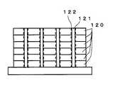
図16は、チップ積層半導体装置の一例の断面模式図を示す。半導体チップ120を多層化した場合には、今までのチップ面内の配線に加えて、さらにチップ間の配線が必要となる。このチップ間の配線として、配線密度を高めるためにチップの半導体基板の表面から裏面を貫通した貫通配線121がある。なお、122は、絶縁膜を示す。非特許文献1には、半導体チップのSi基板を50μmまで薄膜化し、基板に表面から裏面まで貫通する10μm角の孔を開けて、そこにメタルを充填してチップ間配線用の貫通配線を形成している。この貫通配線により、チップ間配線はチップ面内で2次元に配置でき、数百本のチップ間配線も可能になる。このような多層化した半導体チップ間では、貫通配線を介してデータを伝送することが行われる。 FIG. 16 is a schematic cross-sectional view of an example of a chip laminated semiconductor device. When the
図17は、上記の半導体チップ間でデータ伝送を行う伝送回路の一例の構成図を示す。この伝送回路は、送信側チップ10と受信側チップ20との間で貫通配線15を介して1ビット2値のデジタル伝送をする伝送回路である。図18は、図17の伝送回路において2ビット分を並列に伝送した場合の波形図を示す。 FIG. 17 shows a configuration diagram of an example of a transmission circuit that performs data transmission between the semiconductor chips. This transmission circuit is a transmission circuit that performs 1-bit binary digital transmission between the transmission-
図17の伝送回路において、送信側チップ10内のフリップフロップ11からチップ間同期クロックの立ち上がりエッジのタイミングで送信したデータは、出力バッファ12を経て送信側チップ10外へ送られる。図18(A)は、上記のチップ間同期クロックCLKを示す。送信側チップ10は、そのクロックのクロックサイクルの1番目で「1」、2番目で「2」、3番目で「0」、4番目で「3」の値を持つデータを、同図(B)に示すData0と同図(C)に示すData1の1ビット2値で送信する。なお、2ビットを並列で伝送するにはフリップフロップ10及び出力バッファ12からなる回路部が2つ必要である。同様に、受信側チップ20も図17の構成の回路部が2つ必要になる。 In the transmission circuit of FIG. 17, data transmitted from the flip-
送信側チップ10から送信されたデータは、貫通配線15を伝送して受信側のチップ20に入力される。受信側チップ20は、信号入力端子にESD保護素子21が設けられており、受信したデータを入力バッファ22を経て、フリップフロップ23のデータ入力端子に入力する。フリップフロップ23は、そのクロック入力端子に入力されるクロックの立ち上がりエッジのタイミングでデータ入力端子に入力された受信データを取り込む。図18(D)、(E)は、受信側チップ20のフリップフロップ23で取り込まれた1ビット2値の受信データData0、data1を示す。ここで、送信側チップ10のクロックと受信側チップ20のクロックは同期したタイミングを持つ。 The data transmitted from the transmitting
「0」と「1」の2値のデジタル伝送を行う図17の伝送回路においては、伝送データにより貫通配線15の寄生容量と受信側チップ20内のESD保護素子21の容量を充放電する。その充放電回数は、伝送データが「1」から「1」、「1」から「0」、「0」から「0」、「0」から「1」への4つのデータ遷移パターンのうち、「1」から「0」が放電、「0」から「1」が充電となるので、充電あるいは放電が1回で充放電回数が1であると定義すると、1ビット伝送する場合の充放電回数は1クロックサイクルあたり平均0.5回となる。 In the transmission circuit of FIG. 17 that performs binary digital transmission of “0” and “1”, the parasitic capacitance of the through
上記の伝送回路においては、貫通配線15を使ってチップ間の信号伝送を行う際に、貫通配線15の寄生容量とESD保護素子21の容量とを充放電するために大きな電力を消費するという問題がある。すなわち、太さが1μm以下のチップ面内の配線とは異なり、貫通配線は十μm以上の太さが必要である。これは、貫通配線のプロセス同士で貫通配線の位置を合わせるためにチップ間の目合わせ精度である数μmより一桁大きいサイズの貫通配線が必要なためである。 In the above transmission circuit, when signal transmission between chips is performed using the through
貫通配線の太さが大きいために、基板との寄生容量がチップ面内配線と比べて大きい。例えば、断面が直径20μmの円状の貫通配線が250nm厚の絶縁膜を挟んでSi半導体基板を貫通している場合の配線容量は、基板の厚さが50μm、つまり貫通配線長50μmでは0.45pFである。チップ面内で通常使われている面内配線が1mmあたり0.2pF程度であることから、面内配線に比べて貫通配線の寄生容量は単位長さあたり45倍になる。さらに、チップ間伝送の場合には、チップの信号入力端子にESD保護素子をつけることも必要で、これによる付加容量もある。その結果、貫通配線15を使ってチップ間の信号伝送を行う際に、容量を充放電するために大きな電力を消費してしまう。 Since the thickness of the through wiring is large, the parasitic capacitance with the substrate is larger than the in-chip wiring. For example, the wiring capacity in the case where a circular through wiring having a diameter of 20 μm passes through a Si semiconductor substrate with an insulating film having a thickness of 250 nm interposed therebetween is 0.5 when the thickness of the substrate is 50 μm, that is, the through wiring length is 50 μm. 45 pF. Since the in-plane wiring normally used in the chip plane is about 0.2 pF per mm, the parasitic capacitance of the through wiring is 45 times per unit length compared to the in-plane wiring. Further, in the case of inter-chip transmission, it is necessary to attach an ESD protection element to the signal input terminal of the chip, and there is an additional capacity due to this. As a result, when performing signal transmission between chips using the through
このように、貫通配線を使う場合に消費電力が問題となるチップ間伝送において、チップ間伝送の充放電電力を低減するためには、2値デジタル伝送よりも少ない充放電回数で同じデータ量を送る必要がある。言い換えると、同じ充放電回数でより多くのデータ量を送る必要がある。例えば、伝送信号の振幅を多電位にして、より多くの値を伝送する方法がある。多電位を使わない方法としては、パルス幅を多段階にするパルス幅変調してデータを伝送する方法が知られている(例えば、特許文献3参照)。この特許文献3には、1クロックサイクルで異なるパルス幅を使ってデータを多重にして伝送している。 As described above, in order to reduce the charge / discharge power for inter-chip transmission in inter-chip transmission where power consumption is a problem when using through wiring, the same amount of data can be obtained with fewer charge / discharge cycles than in binary digital transmission. I need to send it. In other words, it is necessary to send a larger amount of data with the same number of charge / discharge cycles. For example, there is a method of transmitting more values by setting the amplitude of the transmission signal to multiple potentials. As a method that does not use multiple potentials, a method is known in which data is transmitted by performing pulse width modulation with multiple pulse widths (see, for example, Patent Document 3). In
しかしながら、伝送信号の振幅を多電位にすることで、2値デジタル伝送よりも少ない充放電回数で同じデータ量を送ることで充放電電力を低減する方法は、多電源が必要であることや、低振幅の信号がノイズの影響を受け易いという問題がある。 However, the method of reducing charge / discharge power by sending the same amount of data with a smaller number of charge / discharge cycles than binary digital transmission by making the amplitude of the transmission signal multi-potential requires multiple power sources, There is a problem that low amplitude signals are susceptible to noise.
更に、貫通配線を使う場合に消費電力が問題となるチップ間伝送において、特許文献3に記載されたパルス幅変調したデータを伝送する方法は、以下の問題がある。図19は、パルス幅変調伝送を使って1配線で3ビット分を送る4値伝送の送信波形を示す。ここでは、図19(A)に示すクロックCLKの1クロックサイクル内で4段階のパルス幅を使い、パルス幅が最も短い場合は「0」、以下パルス幅が長くなるほど「1」、「2」、「3」の値のデータを伝送するものとする。従って、図19(B)に示すパルス幅変調された伝送データは、「1」、「2」、「0」、「3」の値の順でデータが伝送される場合を示しており、図18に示したデジタル伝送と同じデータ順である。 Furthermore, the method of transmitting pulse width modulated data described in
ここで、充放電回数は1クロックサイクルあたり充電と放電が1回ずつ、合計2回になる。1ビットで2値のデジタルデータを伝送するデジタル伝送回路と同じデータ量を伝送するには、配線数は半分になるが、充放電回数は2倍になる。パルス幅変調方式の充放電回数を上記のデジタル伝送回路より増やさないためには、1配線で4ビット分の16値伝送よりも大きい多値で伝送することが必要となる。従って、パルス幅変調伝送を行う伝送回路では、上記のデジタル伝送回路よりも消費電力を増やさないためには、クロックサイクルの16分の1よりも小さいパルス幅を生成するための高速クロックあるいは高速遅延制御が必要であるという問題がある。 Here, the number of times of charging / discharging is two times in total, one charge and one discharge per clock cycle. In order to transmit the same amount of data as a digital transmission circuit that transmits binary digital data with 1 bit, the number of wirings is halved, but the number of times of charging and discharging is doubled. In order not to increase the number of times of charge / discharge of the pulse width modulation method as compared with the above digital transmission circuit, it is necessary to perform transmission with a multi-value larger than 16-value transmission for 4 bits with one wiring. Therefore, in a transmission circuit that performs pulse width modulation transmission, a high-speed clock or a high-speed delay for generating a pulse width smaller than 1/16 of a clock cycle in order not to increase power consumption compared to the above-described digital transmission circuit. There is a problem that control is necessary.
本発明は以上の点に鑑みなされたもので、チップ間でデータ伝送する場合に貫通配線を使う場合であっても、多電位伝送のような多電源を用いず、かつ、パルス幅変調データ伝送方式で必要とされる高速クロックあるいは高速遅延制御を用いず、1ビットで2値のデジタルデータを伝送する場合と比べて1クロックサイクルあたりのチップ間配線充放電回数を減らして消費電力を削減し得る伝送方法、伝送回路及び伝送システムを提供することを目的とする。 The present invention has been made in view of the above points, and even when a through wiring is used for data transmission between chips, a multi-power supply such as multi-potential transmission is not used, and pulse width modulation data transmission is performed. Reduces power consumption by reducing the number of inter-chip wiring charge / discharge cycles per clock cycle compared to transmitting binary digital data in one bit without using the high-speed clock or high-speed delay control required by the system. An object is to provide a transmission method, a transmission circuit, and a transmission system.
上記の目的を達成するため、第1の発明の伝送方法は、単一の配線を介して伝送データを伝送する伝送方法において、クロックの1クロックサイクルあたり1回の立ち上がり又は立ち下りの振幅遷移を有し、かつ、クロックのエッジから振幅遷移までの位相により、2ビット以上の値を持つデータを伝送データとして伝送することを特徴とする。 In order to achieve the above object, a transmission method according to a first aspect of the present invention is a transmission method for transmitting transmission data via a single wiring, wherein an amplitude transition of rising or falling once is made per one clock cycle of a clock. And data having a value of 2 bits or more is transmitted as transmission data according to the phase from the clock edge to the amplitude transition.
また、上記の目的を達成するため、第2の発明の伝送回路は、単一の配線へ伝送データを伝送する伝送回路において、クロックをN逓倍(Nは2以上の自然数)して得た逓倍クロックを生成する逓倍クロック生成手段と、逓倍クロックをカウントしてクロックの1クロックサイクルで一巡するカウント値を得るカウント手段と、カウント手段のカウント値と、伝送する2ビット以上のデータの値とを比較する比較手段と、比較手段による比較結果に応じて、クロックの1クロックサイクルあたり1回の立ち上がり又は立ち下りの振幅遷移を有し、かつ、クロックのエッジから振幅遷移までの位相により、2ビット以上の値を持つデータを伝送データとして生成するデータ生成手段とを有することを特徴とする。 In order to achieve the above object, the transmission circuit of the second invention is a multiplication obtained by multiplying a clock by N (N is a natural number of 2 or more) in a transmission circuit that transmits transmission data to a single wiring. A multiplying clock generating means for generating a clock; a counting means for counting the multiplied clocks to obtain a count value that makes a round in one clock cycle of the clock; a count value of the counting means; and a value of data of two or more bits to be transmitted According to the comparison means to be compared and the comparison result by the comparison means, the clock has one rising or falling amplitude transition per clock cycle, and 2 bits depending on the phase from the clock edge to the amplitude transition And a data generation means for generating data having the above values as transmission data.
また、上記の目的を達成するため、第3の発明の伝送回路は、クロックの1クロックサイクルあたり1回の立ち上がり又は立ち下りの振幅遷移を有し、かつ、クロックのエッジから振幅遷移までの位相により、2ビット以上の値を持つデータを単一の配線を介して受信する伝送回路であって、受信したデータの、クロックのエッジから振幅遷移までの位相を検出する位相検出手段と、位相検出手段の検出結果に基づいて、伝送する2ビット以上のデータを復元する復元手段とを有することを特徴とする。 In order to achieve the above object, the transmission circuit according to the third aspect of the present invention has one rising or falling amplitude transition per clock cycle and a phase from the clock edge to the amplitude transition. Is a transmission circuit for receiving data having a value of 2 bits or more via a single wiring, and a phase detection means for detecting the phase of the received data from the edge of the clock to the amplitude transition, and phase detection And restoring means for restoring data of 2 bits or more to be transmitted based on the detection result of the means.
更に、上記の目的を達成するため、第4の発明の伝送システムは、第1の半導体チップから単一のチップ間配線を介して第2の半導体チップへ伝送データを伝送する伝送システムにおいて、上記の第1の半導体チップは、
クロックをN逓倍(Nは2以上の自然数)して得た逓倍クロックを生成する逓倍クロック生成手段と、逓倍クロックをカウントしてクロックの1クロックサイクルで一巡するカウント値を得るカウント手段と、カウント手段のカウント値と、伝送する2ビット以上のデータの値とを比較する比較手段と、比較手段による比較結果に応じて、クロックの1クロックサイクルあたり1回の立ち上がり又は立ち下りの振幅遷移を有し、かつ、クロックのエッジから振幅遷移までの位相により、2ビット以上の値を持つデータを伝送データとして生成するデータ生成手段と、を有し、
上記の第2の半導体チップは、
チップ間配線を介して第1の半導体チップから受信した受信データの、クロックのエッジから振幅遷移までの位相を検出する位相検出手段と、位相検出手段の検出結果に基づいて、伝送する2ビット以上のデータを復元する復元手段と、を有することを特徴とする。Furthermore, in order to achieve the above object, a transmission system according to a fourth aspect of the present invention is a transmission system for transmitting transmission data from a first semiconductor chip to a second semiconductor chip via a single interchip wiring. The first semiconductor chip of
A multiplying clock generating means for generating a multiplied clock obtained by multiplying the clock by N (N is a natural number of 2 or more), a counting means for counting the multiplied clock and obtaining a count value that makes a round in one clock cycle of the clock; The comparison means for comparing the count value of the means and the value of the data of 2 bits or more to be transmitted, and there is one rising or falling amplitude transition per clock cycle according to the comparison result by the comparison means. And data generation means for generating data having a value of 2 bits or more as transmission data according to the phase from the edge of the clock to the amplitude transition,
The second semiconductor chip is
Phase detection means for detecting the phase of the received data received from the first semiconductor chip via the inter-chip wiring from the clock edge to the amplitude transition, and two or more bits to be transmitted based on the detection result of the phase detection means And restoring means for restoring the data.
本発明によれば、複数の半導体チップを積層又は同一面上に並べた半導体装置において、2ビット以上のデータを半導体チップ間で伝送する際に、振幅遷移の位相及び/又は配線選択を使って1クロックサイクルあたりの配線充放電回数を減らすことで、半導体装置の消費電力の低減が実現できる。 According to the present invention, in a semiconductor device in which a plurality of semiconductor chips are stacked or arranged on the same surface, when data of 2 bits or more is transmitted between the semiconductor chips, the phase of amplitude transition and / or wiring selection is used. By reducing the number of wiring charges / discharges per clock cycle, the power consumption of the semiconductor device can be reduced.
次に、本発明の実施形態について図面を参照して詳細に説明する。 Next, embodiments of the present invention will be described in detail with reference to the drawings.
本発明は、伝送信号がクロックサイクルあたり1回の立ち上がり、あるいは立ち下がり振幅遷移を持ち、その立ち上がり、あるいは立ち下がりエッジのクロックエッジからの位相によって2ビット以上のデータを伝送することを特徴とする。また、本発明は、クロックサイクル毎に立ち上がりと立ち下がりの振幅遷移を交互に伝送することを特徴とする。また、伝送に使う配線を複数備え、クロックサイクルあたり1つの配線を選択して振幅遷移することを特徴とする。 The present invention is characterized in that a transmission signal has a rising or falling amplitude transition once per clock cycle, and data of 2 bits or more is transmitted depending on the phase from the clock edge of the rising or falling edge. . Further, the present invention is characterized in that rising and falling amplitude transitions are alternately transmitted every clock cycle. In addition, a plurality of wirings used for transmission are provided, and one wiring is selected per clock cycle and amplitude transition is performed.
(第1の実施形態)
図1は、本発明になる伝送回路及び伝送システムの第1の実施形態のブロック図を示す。本実施形態は、8つの位相を使った多相伝送である8相伝送の構成である。(First embodiment)
FIG. 1 shows a block diagram of a first embodiment of a transmission circuit and a transmission system according to the present invention. The present embodiment has a configuration of eight-phase transmission that is multiphase transmission using eight phases.
そこで、まず、多相伝送について説明する。図2は多相伝送方式の一例の伝送波形を示す。図2(B)は、時間軸を4分割してデータエッジをずらした4相伝送波形を示しており、同図(A)に示すクロックCLKの立ち上がりエッジからのデータ振幅の立ち上がり(あるいは、立ち下がり)の位相を使った多相伝送方式の送信波形を示す。 First, multiphase transmission will be described. FIG. 2 shows a transmission waveform of an example of the multiphase transmission system. FIG. 2B shows a four-phase transmission waveform in which the data axis is shifted by dividing the time axis into four, and the rise (or rise) of the data amplitude from the rising edge of the clock CLK shown in FIG. The transmission waveform of the multiphase transmission method using the phase of (falling) is shown.
図2に示す4相伝送方式では、図19のパルス幅変調伝送方式と同じデータ量を同じ配線数で伝送することになるが、充放電回数は半分で済む。この4相を使った伝送では、図17に示した伝送回路で2ビットデータを伝送する場合と、同じ充放電回数になる。従って、2ビットデータを伝送する伝送回路よりも充放電回数を減らすことで低消費電力化するためには、4相よりも多い位相を使って伝送することになる。 In the four-phase transmission method shown in FIG. 2, the same amount of data as in the pulse width modulation transmission method in FIG. 19 is transmitted with the same number of wires, but the number of times of charging / discharging is halved. In the transmission using the four phases, the number of times of charging / discharging is the same as that in the case where 2-bit data is transmitted by the transmission circuit shown in FIG. Therefore, in order to reduce power consumption by reducing the number of times of charging / discharging as compared with a transmission circuit that transmits 2-bit data, transmission is performed using more phases than four phases.
図3は8相伝送波形の一例を示す波形図である。すなわち、図3(B)は、時間軸を8分割してデータエッジをずらした8相伝送波形を示しており、同図(A)に示すクロックCLKの立ち上がりエッジからのデータ振幅の立ち上がり(あるいは、立ち下がり)の位相を使った8相伝送方式の送信波形を示す。1つのチップ間配線にて8相伝送方式でデータ伝送する場合には、後述するように3ビットデータを伝送できるので、チップ間回線の充放電回数は、図17に示したデジタル伝送回路を使って2ビットを伝送する場合の充放電回数の2/3になる。 FIG. 3 is a waveform diagram showing an example of an 8-phase transmission waveform. That is, FIG. 3B shows an 8-phase transmission waveform in which the data axis is shifted by dividing the time axis into eight, and the rising edge of the data amplitude from the rising edge of the clock CLK shown in FIG. The transmission waveform of the 8-phase transmission system using the phase of (falling). In the case of data transmission by the 8-phase transmission method with one interchip wiring, since 3-bit data can be transmitted as will be described later, the charge / discharge frequency of the interchip line uses the digital transmission circuit shown in FIG. Therefore, it becomes 2/3 of the number of times of charge / discharge when 2 bits are transmitted.
さらに、16相伝送方式の場合は1つのチップ間配線にて4ビットデータを伝送することができるので、その場合の充放電回数は、図17に示したデジタル伝送回路により2ビットデータを伝送する場合に比べて充放電回数を半分まで減らすことができ、低消費電力化することが可能になる。 Furthermore, in the case of the 16-phase transmission method, 4-bit data can be transmitted by one inter-chip wiring. In this case, the charge / discharge frequency is transmitted by 2-bit data by the digital transmission circuit shown in FIG. Compared to the case, the number of times of charging / discharging can be reduced to half, and the power consumption can be reduced.
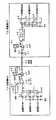
再び図1に戻って説明する。本実施形態の伝送システムは、送信側の半導体チップ(以下、送信側チップという)30と受信側の半導体チップ(以下、受信側チップという)40とが貫通配線50で接続されており、送信側チップ30からデータを8相伝送方式で貫通配線50を介して受信側チップ40へ伝送する。送信側チップ30と受信側チップ40とは、実際には図5の斜視図に模式的に示すように積層され、それらの間のチップ間配線を貫通配線50とした構成であるが、図1では説明の便宜上、送信側チップ30と受信側チップ40とを横に並べて、3ビット伝送に必要な回路と貫通配線50だけを図示している。 Returning again to FIG. In the transmission system of the present embodiment, a transmission-side semiconductor chip (hereinafter referred to as a transmission-side chip) 30 and a reception-side semiconductor chip (hereinafter referred to as a reception-side chip) 40 are connected by a through
図1において、送信側チップ30は、各々1ビットの送信データData0、Data1、Data2がデータ入力端子に入力されるフリップフロップ31、32、33と、クロックCLKを8逓倍したクロックCK8をカウントするカウンタ34と、入力端子A、Bにそれぞれ入力された3ビットのデータの値を大小比較するデジタルコンパレータ35と、クロックCLKを1/2倍の周波数に分周する分周器36と、デジタルコンパレータ35の出力信号又はその逆極性の出力信号を選択するセレクタ37と、出力バッファ38とからなる。 In FIG. 1, a transmitting-side chip 30 includes flip-
また、受信側チップ40は、入力端子に接続されたESD保護素子41と、受信データを緩衝増幅する入力バッファ42と、クロックCLKを1/2倍の周波数に分周する分周器43と、入力信号又はその逆極性の入力信号を選択するセレクタ44と、クロックCLKを8逓倍したクロックCK8をダウンカウントするダウンカウンタ45と、ダウンカウンタ45の3ビットの出力信号の各ビットがそれぞれデータ入力端子に供給されるフリップフロップ46、47及び48とからなる。 The receiving-
次に、本実施形態の動作について、図4のフローチャートを併せ参照して説明する。まず、送信側チップ30の内部の3ビットの送信データは、図4(B)、(C)、(D)に示すように各1ビットの送信データ0、1、2とされて、フリップフロップ31、32、33に同図(A)に示すクロックCLKの立ち上がりに同期して取り込まれた後、デジタルコンパレータ35の入力端子Aに3ビットデータとして印加される。 Next, the operation of the present embodiment will be described with reference to the flowchart of FIG. First, as shown in FIGS. 4B, 4C, and 4D, the 3-bit transmission data inside the transmission-side chip 30 is converted into 1-
一方、8ビットのカウンタ34は、上記のクロックCLKの周波数を8逓倍して得られた図4(E)に示すクロックCK8をアップカウントすることにより、同図(F)に示すように、値が「0」から1ずつカウントアップしていき「7」に達した後「0」に戻るような、値が「0」〜「7」で一巡する3ビットのカウント値をデジタルコンパレータ35へ出力する。デジタルコンパレータ35は、入力端子Aに入力されるフリップフロップ31〜33からの3ビットの送信データと、入力端子Bに入力されるカウンタ34からの3ビットのカウンタ値とを大小比較し、入力端子Aの入力の値が入力端子Bの入力の値以下であるとき、すなわちカウンタ値が3ビットの送信データの値以上であるときに、図4(G)に示すようにハイレベルの信号を出力し、それ以外の場合はローレベルの信号を出力する。 On the other hand, the 8-bit counter 34 counts up the clock CK8 shown in FIG. 4 (E) obtained by multiplying the frequency of the clock CLK by 8 as shown in FIG. Counts up from “0” by 1 and reaches “7” and then returns to “0”. Outputs to the digital comparator 35 a 3-bit count value that goes around from “0” to “7”. To do. The
セレクタ37は、デジタルコンパレータ35から出力された信号と同一極性の信号と逆極性の信号とを、分周器36からのクロックCLKの1/2倍の周波数の制御信号に基づいて、1クロックサイクル毎に交互に選択する。従って、このセレクタ37からは、1クロックサイクルで立ち上がりか立ち下がりのいずれかに1回振幅遷移する波形の、図4(H)に示す信号が出力される。ここで、上記のカウンタ値は、立ち上がりあるいは立ち下がりエッジのクロックエッジからの位相(1クロックサイクル180度を8分割した分割単位の位相)を示しており、セレクタ37の出力信号の振幅遷移の位置(位相)によって「0」〜「7」までの値をもつ3ビットのデータの値を識別させることができる。出力バッファ38は、このセレクタ37から出力された信号を送信側チップ30の外部の貫通配線50へ出力する。 The
受信側チップ40では、貫通配線50から入力した図4(H)に示す信号を入力バッファ42で受けてセレクタ44に受信データとして供給する。セレクタ44は、入力バッファ42から出力された信号と同一極性の信号と逆極性の信号とを、分周器43からのクロックCLKの1/2倍の周波数の制御信号に基づいて、1クロックサイクル毎に交互に選択してダウンカウンタ45のリセット端子RSTに入力する。このダウンカウンタ45のリセット端子RSTの入力信号(以下、リセット信号ともいう)は、図4(I)に示される。 In the
ダウンカウンタ45は、クロックCLKの周波数を8逓倍して得られた図4(E)に示すクロックCK8をダウンカウントする。ここで、ダウンカウンタ45は、リセット信号がローレベルの時には3ビットの最大値「7」を出力し、リセット信号がハイレベルの時にはクロックCK8に同期して値が「7」から1ずつカウントダウンしていき「0」に達した後「7」に戻るような、値が「7」〜「0」で一巡する3ビットのカウント値を出力する。ダウンカウンタ45のリセットはクロック同期式であり、リセット値が変化した次のクロックでカウント値はリセットされる。 The down counter 45 down-counts the clock CK8 shown in FIG. 4E obtained by multiplying the frequency of the clock CLK by 8. Here, the down counter 45 outputs a 3-bit maximum value “7” when the reset signal is at a low level, and counts down one by one from “7” in synchronization with the clock CK8 when the reset signal is at a high level. A 3-bit count value is output that goes round from “7” to “0” so as to return to “7” after reaching “0”. The down counter 45 is reset in a clock synchronous manner, and the count value is reset at the next clock whose reset value has changed.
これにより、ダウンカウンタ45からは、図4(J)に示すような値の3ビットの信号が出力されて、その各1ビットがフリップフロップ46、47及び48の各データ入力端子に印加される。フリップフロップ46、47及び48は、図4(A)に示すチップ間同期クロックCLKがクロック端子に共通に印加されており、このチップ間同期クロックCLKの例えば立ち上がりのタイミングで、データ入力端子に印加された信号を取り込む。その結果、フリップフロップ46、47及び48のQ出力端子からは、図4(K)、(L)、(M)に示すように、送信側チップ30から送信されたデータと同じ値の各1ビットのデータが取り出され、3ビットデータに復元されて、受信側チップ40の内部の回路(図示せず)へと送られる。 As a result, a 3-bit signal having a value as shown in FIG. 4J is output from the down counter 45, and each 1 bit is applied to each data input terminal of the flip-
この本実施形態によれば、8相伝送により1クロックサイクルあたり1回振幅遷移する波形の伝送データを貫通配線50を介して受信側チップ40へ伝送するため、貫通配線50の1クロックサイクルあたり1回の充放電で送信側チップ30から受信側チップ40へ3ビットデータを伝送することができる。これにより、本実施形態によれば、3ビットデータを3つの貫通配線を使って伝送する伝送回路と比べて配線の充放電回数を2/3に減らすことができ、容量の大きい貫通配線50からなるチップ間配線とESD保護素子41を用いたチップ間伝送を低消費電力にすることができる。 According to the present embodiment, transmission data having a waveform that undergoes an amplitude transition once per clock cycle by 8-phase transmission is transmitted to the receiving-
すなわち、本実施形態によれば、チップ間でデータ伝送する場合に貫通配線を使う場合であっても、多電位伝送のような多電源を用いず、かつ、パルス幅変調データ伝送方式で必要とされる高速クロックあるいは高速遅延制御を用いず、1ビットで2値のデジタルデータを伝送する場合と比べて1クロックサイクルあたりのチップ間配線充放電回数を減らして消費電力を削減することができる。 That is, according to the present embodiment, even when using a through wiring for data transmission between chips, a multi-power supply such as multi-potential transmission is not used and a pulse width modulation data transmission method is required. Compared with the case where binary digital data is transmitted by 1 bit without using the high-speed clock or high-speed delay control, the power consumption can be reduced by reducing the number of inter-chip wiring charge / discharge per clock cycle.
なお、本実施の形態は8相伝送であるが、図17に示したデジタル伝送回路よりも充放電回数を減らすためには、4相よりも大きい位相の数であればよい。例えば、16相伝送では、1クロックサイクルで4ビット分のデータを1回の充放電で伝送できるので、充放電回数は図17に示したデジタル伝送回路よりも半減し、消費電力を8相伝送よりもさらに低減することができる。 Although this embodiment uses 8-phase transmission, the number of phases may be larger than 4 phases in order to reduce the number of charge / discharge cycles as compared with the digital transmission circuit shown in FIG. For example, in 16-phase transmission, data of 4 bits can be transmitted in one charge / discharge in one clock cycle, so the number of times of charging / discharging is halved compared to the digital transmission circuit shown in FIG. Can be further reduced.
(第2の実施形態)
図6は、本発明になる伝送回路及び伝送システムの第2の実施形態のブロック図を示す。同図中、図1と同一構成部分には同一符号を付し、その説明を省略する。本実施形態も、第1の実施形態と同様に8つの位相を使った多相伝送である8相伝送の構成である。本実施形態は、図1の第1の実施形態と比べて、送信側チップ60のセレクタ37と出力バッファ38の間に8逓倍のクロックCK8がクロック入力端子に印加されるフリップフロップ61を追加している点に特徴がある。(Second Embodiment)
FIG. 6 shows a block diagram of a second embodiment of a transmission circuit and a transmission system according to the present invention. In the figure, the same components as those in FIG. The present embodiment also has an 8-phase transmission configuration that is multiphase transmission using eight phases, as in the first embodiment. Compared with the first embodiment of FIG. 1, this embodiment adds a flip-
図7は図6の各部の信号波形図を示す。図7(A)に示すクロックCLK、同図(B)〜(D)に示す3ビットの送信データ、同図(E)に示す8逓倍クロックCK8、同図(F)に示すカウンタ35の出力カウンタ値、同図(G)に示すデジタルコンパレータ35の出力信号は、図4(A)〜(G)の各信号と同一である。また、図7(J)〜(M)に示す信号も、図4(J)〜(M)に示す信号と同一である。フリップフロップ61を設けることにより、出力バッファ38から貫通配線50への出力波形に、セレクタ37の選択切り替え時のノイズパルスがのることを避けることができる。 FIG. 7 is a signal waveform diagram of each part of FIG. The clock CLK shown in FIG. 7A, the 3-bit transmission data shown in FIGS. 7B to 7D, the 8-times clock CK8 shown in FIG. 7E, and the output of the
ただし、本実施形態では、フリップフロップ61を追加したことにより、チップ間伝送波形、すなわちフリップフロップ61から出力バッファ38を介して貫通配線50へ出力される信号波形は、図7(H)に示す如くになり、これによりダウンカウンタ45のリセット信号波形も図7(I)に示す如くになり、それぞれクロックCLKの1クロックサイクルの8分の1だけ遅延する。そこで、本実施形態では、受信側のダウンカウンタ45のリセットはクロック非同期式にして、リセット値が変化した時にすぐにカウンタ値の出力をリセットする。 However, in this embodiment, by adding the flip-
(第3の実施形態)
図8は、本発明になる伝送回路及び伝送システムの第3の実施形態の送信側チップのブロック図を示す。同図中、図1と同一構成部分には同一符号を付し、その説明を省略する。本実施形態の送信側チップ70は、チップ内部の3ビットのデータを、8逓倍のクロックCK8を使ってカウンタ34で生成された3ビットのアップカウント値と比較して、同じ値になった時にハイレベルの信号を出力するデジタルコンパレータ71を使用する。(Third embodiment)
FIG. 8 shows a block diagram of a transmission-side chip of the third embodiment of the transmission circuit and transmission system according to the present invention. In the figure, the same components as those in FIG. The transmitting-side chip 70 of the present embodiment compares the 3-bit data inside the chip with the 3-bit up-count value generated by the
図9(A)はクロックCLKの波形、同図(B)〜(D)は3ビットの送信データData0〜Data2、同図(E)は上記の8逓倍したクロックCK8の波形、同図(F)はカウンタ34の出力カウント値を示す。これにより、デジタルコンパレータ71の出力信号は、図9(G)に示すように、3ビットの送信データの値とカウンタ34の出力カウント値とが一致したときにのみ、ハイレベルとなる。 9A shows the waveform of the clock CLK, FIGS. 9B to 9D show the 3-bit transmission data Data0 to Data2, FIG. 9E shows the waveform of the clock CK8 multiplied by 8 and FIG. ) Indicates the output count value of the
図8において、デジタルコンパレータ71の出力信号は、セレクタ72の制御信号として供給される。セレクタ72は、出力信号をフリップフロップ73のデータ入力端子に供給する。フリップフロップ73は、8逓倍したクロックCK8がクロック入力端子に入力され、Q出力端子の出力信号を出力バッファ38とセレクタ72の非反転入力端子と反転入力端子にそれぞれ供給する。セレクタ72はデジタルコンパレータ71からの制御信号がハイレベルとなった時に、フリップフロップ73から出力された信号を極性反転して(すなわち、反転入力端子に入力された信号を出力して)フリップフロップ73のデータ入力端子に供給する。これにより、フリップフロップ73からは図9(H)に示す信号が送信データとして出力される。この送信データの波形は、図7(H)に示した第2の実施形態の送信データと同様の波形である。 In FIG. 8, the output signal of the
本実施形態の送信側チップ70から出力された送信データを、貫通配線を通して受信する受信側チップの構成は、図6の受信側チップ40と同一構成である。また、その受信側チップの各部の信号波形は、図7と同様である。 The configuration of the receiving side chip that receives the transmission data output from the transmitting side chip 70 of the present embodiment through the through wiring is the same as the configuration of the receiving
本実施形態も、フリップフロップ73を設けることにより、出力バッファ38から貫通配線への出力波形に、セレクタ72の選択切り替え時のノイズパルスがのることを避けることができる。 Also in this embodiment, by providing the flip-
(第4の実施形態)
図10は、本発明になる伝送回路及び伝送システムの第4の実施形態のブロック図を示す。本実施形態は、上記の各実施形態における多相伝送に加えて、更に充放電回数を減らすために配線選択を使った多線伝送を併用した場合の構成である。(Fourth embodiment)
FIG. 10 shows a block diagram of a fourth embodiment of the transmission circuit and transmission system according to the present invention. In this embodiment, in addition to the multi-phase transmission in each of the above-described embodiments, a multi-line transmission using wiring selection is used in combination in order to further reduce the number of times of charging and discharging.
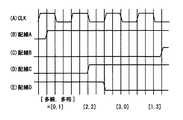
そこで、まず、多相伝送に多線伝送を併用した場合について図11の波形図と共に説明する。多相伝送では、1クロックサイクルで1本の配線について必ず立ち上がりあるいは立ち下がりのいずれかに振幅を遷移させる。これに対し、多線伝送の併用では、複数の配線を備え、1クロックサイクルでいずれか一本の配線を選択して、立ち上がりあるいは立ち下がりのいずれかで振幅遷移させる。これにより、どの配線を使ったかという情報が付加される。 First, the case where multi-line transmission is used in combination with multi-phase transmission will be described with reference to the waveform diagram of FIG. In multiphase transmission, the amplitude is always shifted to either rising or falling for one wiring in one clock cycle. On the other hand, in the combined use of multi-line transmission, a plurality of wirings are provided, and any one wiring is selected in one clock cycle, and amplitude transition is performed at either rising or falling. Thereby, information on which wiring is used is added.
図11の場合には、(A)に示すクロックCLKの連続する4つのクロックサイクルのうちの何番目のクロックサイクルで伝送データの立ち上がり又は立ち下りの振幅遷移があるかにより、伝送する4本のチップ間配線A〜Dのどの配線を使用しているかを示している。すなわち、図11(A)に示す1番目のクロックサイクルで伝送データの立ち上がりがあるときは同図(B)に示すように配線Aを、2番目のクロックサイクルで伝送データの立ち上がりがあるときは同図(D)に示す配線Cを、3番目のクロックサイクルで立ち下がりがあるときは同図(E)に示すように配線Dを、4番目のクロックサイクルで立ち上がりがあるときは同図(C)に示すように配線Bを、それぞれ選んでその配線で伝送されるように、信号の立ち上がりあるいは立ち下がりエッジを発生させてデータ伝送している。 In the case of FIG. 11, four transmission lines are transmitted depending on the number of clock cycles among the four consecutive clock cycles of the clock CLK shown in FIG. It shows which of the inter-chip wirings A to D is used. That is, when transmission data rises in the first clock cycle shown in FIG. 11A, the wiring A is connected as shown in FIG. 11B, and transmission data rises in the second clock cycle. When the wiring C shown in FIG. 4D falls at the third clock cycle, the wiring D shows the rising edge at the fourth clock cycle as shown in FIG. As shown in (C), data is transmitted by generating a rising edge or a falling edge of a signal so that the wiring B is selected and transmitted through the wiring.
この配線選択の多線伝送では、各クロックサイクルで2ビット相当のデータ量になる。更に、4相伝送も同時に行う場合は、立ち上がりあるいは立ち下がりのエッジは各サイクルで位相を変えて2ビット分の情報を載せることができる。従って、4相4線伝送では、1クロックサイクルあたり合計で4ビット分のデータ伝送を1回の充放電で行うことができる。これにより、時間軸で4分割しかしていないにもかかわらず、図17に示したデジタル伝送回路の充放電回数と比べて、同じデータ量を送るのに半分の充放電回数にすることができ、消費電力を低減することができる。 In multi-line transmission with this wiring selection, the data amount is equivalent to 2 bits in each clock cycle. Further, when four-phase transmission is also performed at the same time, two-bit information can be loaded by changing the phase of each rising or falling edge in each cycle. Therefore, in the four-phase four-wire transmission, data transmission for a total of 4 bits per clock cycle can be performed by one charge / discharge. Thereby, although it is only divided into four on the time axis, the number of times of charging / discharging can be reduced to half to send the same amount of data compared to the number of times of charging / discharging of the digital transmission circuit shown in FIG. Power consumption can be reduced.
再び図10に戻って説明する。本実施形態は、送信側チップ80から4ビットの送信データを4本の貫通配線110a〜110dで受信側チップ90に伝送する4相4線式伝送の伝送システムである。ここで、それぞれ半導体チップである送信側チップ80と受信側チップ90を積層し、チップ間配線を貫通配線としたものである。しかし、図10では説明の便宜上、送信側チップ80と受信側チップ90を横に並べて、4ビットデータの伝送に必要な回路とチップ間配線のみを図示した。 Returning again to FIG. The present embodiment is a transmission system of four-phase four-wire transmission that transmits four-bit transmission data from the transmission-
送信側チップ80は、各々1ビットの送信データData0、Data1、Data2、Data3がデータ入力端子に入力されるフリップフロップ81a、81b、81c、81dと、クロックCLKを4逓倍したクロックCK4をアップカウントするカウンタ82と、入力端子A、Bにそれぞれ入力された2ビットのデータの値の一致/不一致を検出するデジタルコンパレータ83と、2ビットのデータをデコードして4ビットデータを出力するデコーダ(DEC)84と、デコーダ84からの各ビットとデジタルコンパレータ83の出力信号との論理積をとるAND回路85a、85b、85c、85dと、セレクタ86a、86b、86c、86dと、クロックCK4に同期してセレクタ86a、86b、86c、86dの各出力信号を取り込むフリップフロップ87a、87b、87c、87dと、出力バッファ88a、88b、88c、88dとからなる。 The transmitting-
また、受信側チップ90は、貫通配線110a、110b、110c、11dに接続されている入力端子に接続されたESD保護素子91a、91b、91c、91dと、受信データの各1ビットを緩衝増幅する入力バッファ92a、92b、92c、92dと、2段の排他的論理和(以下、XORと記す)回路93と、クロックCLKを1/4周期位相シフトして得た1/4シフトCLKに同期して動作するフリップフロップ94a、94b、94c、94dと、フリップフロップ94a、94b、94c、94dの入力信号と出力信号がそれぞれ供給される2入力XOR回路95a、95b、95c、95dと、クロックCLKを1/2倍の周波数に分周する分周器96と、入力信号又はその逆極性の入力信号を選択するセレクタ97と、クロックCLKを4逓倍したクロックCK4をダウンカウントするダウンカウンタ98と、XOR回路95a〜95dの各出力信号をエンコードするエンコーダ(ENC)99と、ダウンカウンタ98の2ビットの出力信号の各ビットがそれぞれデータ入力端子に供給されるフリップフロップ100a及び100bと、エンコーダ99の2ビットの出力信号の各ビットがそれぞれデータ入力端子に供給されるフリップフロップ100c及び100dとからなる。 Further, the receiving chip 90 buffers and amplifies the
次に、本実施形態の動作について、図12のフローチャートを併せ参照して説明する。まず、送信側チップ80は、内部の4ビット送信データの各1ビットデータData0、Data1、Data2、Data3(図12(B)、(C)、(D)、(E))をフリップフロップ81a、81b、81c、81dにより、図12(A)に示すクロックCLKの立ち上がりに同期して取り込む。なお、4ビット送信データは、Data0がLSB、Data3がMSBであるものとする。 Next, the operation of this embodiment will be described with reference to the flowchart of FIG. First, the transmitting-
4相伝送のために、フリップフロップ81a、81b、81c、81dに取り込まれた各1ビットの送信データのうち、下位側の2ビットの送信データはフリップフロップ81a、81bからデジタルコンパレータ83の入力端子Bに入力され、上位側の2ビットの送信データはフリップフロップ81c、81dからデコーダ84に供給される。 Of the 1-bit transmission data fetched by the flip-flops 81a, 81b, 81c, 81d for four-phase transmission, the lower-order 2-bit transmission data is input from the flip-flops 81a, 81b to the input terminal of the
デジタルコンパレータ83は、図12(F)に示す4逓倍クロックCK4をアップカウントするカウンタ82から出力される同図(G)に示す2ビットのカウント値の値と、フリップフロップ81a、81bから出力される下位側2ビットの送信データとの値とが一致するかどうか検出し、図12(H)に示すように、一致する時ハイレベルの信号を出力し、不一致の時はローレベルの信号を出力する。 The
4線伝送のために、デコーダ84は、フリップフロップ81c、81dから出力される4ビット送信データの残りの上位側の2ビット送信データの値に基づいて、クロックCLKの1クロックサイクルあたり4つの出力信号の一つがハイレベルになるようにデコードする。このデコーダ84から出力された4つの出力信号の1つずつと、デジタルコンパレータ83から出力された信号とをAND回路85a〜85dは、それぞれ論理積演算をして、その出力信号をセレクタ86a〜86dに制御信号として別々に供給する。 For the 4-wire transmission, the decoder 84 outputs four outputs per one clock cycle of the clock CLK based on the value of the remaining high-order 2-bit transmission data of the 4-bit transmission data output from the flip-flops 81c and 81d. Decode so that one of the signals goes high. The AND circuits 85a to 85d perform an AND operation on each of the four output signals output from the decoder 84 and the signal output from the
セレクタ86a〜86dは、4逓倍クロックCK4に同期して動作するフリップフロップ87a〜87dの各Q出力信号が非反転入力端子と反転入力端子とに供給され、制御信号がハイレベルになった時に反転入力端子に入力されるQ出力信号を選択出力し、制御信号がローレベルの時には、非反転入力端子に入力されるQ出力信号を選択出力する。セレクタ86a〜86dの各出力信号は、フリップフロップ86a〜86dにより4逓倍クロックCK4に同期して取り込まれた後、フリップフロップ86a〜86dのQ出力端子から出力バッファ88a〜88dを経由して送信側チップ80の外部の貫通配線110a〜110dへ出力される。 The selectors 86a to 86d are supplied when the Q output signals of the flip-flops 87a to 87d operating in synchronization with the quadruple clock CK4 are supplied to the non-inverting input terminal and the inverting input terminal, respectively, and inverted when the control signal becomes high level. The Q output signal input to the input terminal is selectively output. When the control signal is at the low level, the Q output signal input to the non-inverting input terminal is selectively output. The output signals of the selectors 86a to 86d are captured by the flip-flops 86a to 86d in synchronization with the quadruple clock CK4, and then transmitted from the Q output terminals of the flip-flops 86a to 86d via the output buffers 88a to 88d. It is output to the through wirings 110 a to 110 d outside the
これにより、貫通配線110a、110b、110c、110dにより伝送される信号は、図12(I)、(J)、(K)、(L)に示すように、クロックCLKの1クロックサイクルで、4本の貫通配線110a〜110dで伝送される信号のうちの一本の貫通配線で伝送される信号のみが振幅遷移し、その立ち上がりあるいは立ち下がりのエッジはクロック立ち上がりエッジから4相のいずれかの位相ずれをもつ。 As a result, signals transmitted through the through-
受信側チップ90は、4本の貫通配線110a〜110dから入力した信号を入力バッファ92a〜92dで受信データとして受ける。受信側チップ90は、これらの受信データを送信側チップ80の内部の送信データと同じ4ビットのデジタルデータに復元するために、4相から2ビット分、4線から2ビット分を戻す。 The receiving-side chip 90 receives signals input from the four through wirings 110a to 110d as received data by the input buffers 92a to 92d. The receiving side chip 90 restores the received data by 4 bits from the 4 phases and 2 bits from the 4 lines in order to restore the received data to the same 4-bit digital data as the transmission data inside the transmitting
受信側チップ90は、4相伝送から2ビット分を戻すために、2段のXOR回路93、分周器96、セレクタ97、ダウンカウンタ98、フリップフロップ100a及び100bからなる回路部を用いる。すなわち、まず、2段のXOR回路93は、入力バッファ92a〜92dから出力される4つの受信データのうちの一つが振幅遷移したときに振幅遷移する図12(M)に示すような信号を出力する。セレクタ97は、このXOR回路93の出力信号を反転入力端子と、非反転入力端子に供給され、分周器96からのクロックCLKの1クロックサイクル毎に反転する制御信号に基づいて、XOR回路93の出力信号と同極性の信号と極性反転した信号とを1クロックサイクル毎に交互に選択してダウンカウンタ98のリセット端子RSTに入力する。 The receiving-side chip 90 uses a circuit unit including a two-
ダウンカウンタ98は、セレクタ97からリセット端子RSTに供給される図12(N)に示すリセット信号がローレベルの場合には、2ビットの最大値「3」を出力し、リセット信号がハイレベルになると4逓倍クロックCK4に同期してカウントダウンする。従って、ダウンカウンタ98からは図12(O)に示すカウント値の2ビット信号が出力される。フリップフロップ100a、100bは、ダウンカウンタ98から出力される上記の2ビットの信号の各1ビットがデータ入力端子に供給され、クロックCLKをその1/4クロックサイクル分位相シフトして得た図12(R)に示す1/4シフトCLKの立ち上がりのタイミングでデータ入力端子に入力されたデータを取り込んだ後、Q出力端子から出力する。これにより、フリップフロップ100a、100bのQ出力端子からは、図12(P)、(Q)に示す各1ビットの信号が出力されて受信側チップ90の内部の回路(図示せず)へ送られる。これにより、4相伝送された信号が元の下位2ビットのデジタル信号に戻されたことになる。 When the reset signal shown in FIG. 12 (N) supplied from the
一方、受信側チップ90は、4線伝送から2ビット分を戻すために、フリップフロップ94a〜94d、XOR回路95a〜95d、エンコーダ99、フリップフロップ100c及び100dからなる回路部を用いる。すなわち、まず、フリップフロップ94a〜94dは、入力バッファ92a〜92dからの各1ビットの受信データのそれぞれを、1/4シフトCLKに同期して出力する。続いて、XOR回路95a〜95dは、上記のフリップフロップ94a〜94dのQ出力端子からの出力信号と、そのデータ入力端子の入力受信データとを入力として受け、1クロックサイクル前の信号から値が変化するときにハイレベルの信号を出力する。これにより、XOR回路95a、95b、95c、95dの各出力信号は、図12(S)、(T)、(U)、(V)に示す如くになる。 On the other hand, the receiving-side chip 90 uses a circuit unit including flip-
エンコーダ99は、これらXOR回路95a〜95dから出力された信号を入力として受け、その入力信号に基づいて、4本の貫通配線110a〜110dの伝送信号のうちのどの貫通配線の伝送信号が振幅遷移したかを示す2ビットデータに変換する。すなわち、エンコーダ99は、XOR回路95a〜95dの各出力信号のうち、XOR回路95aの出力信号のみハイレベルのときは「00」、XOR回路95bの出力信号のみハイレベルのときは「10」、XOR回路95cの出力信号のみハイレベルのときは「01」、XOR回路95dの出力信号のみハイレベルのときは「11」の2ビットデータに変換する。 The
フリップフロップ100c、100dは、エンコーダ99から出力された上記の2ビットデータの1ビット目と2ビット目がデータ入力端子にそれぞれ印加され、それを1/4シフトCLKの立ち上がりのタイミングで取り込んだ後、Q出力端子より出力する。これにより、フリップフロップ100c、100dのQ出力端子からは、図12(W)、(X)に示す各1ビットの信号が出力されて受信側チップ90の内部の回路(図示せず)へ送られる。これにより、4線伝送された信号が元の上位2ビットのデジタル信号に戻されたことになる。こうして、フリップフロップ100a〜100dからは4相の2ビット分とを合わせて、4相4線で4ビット分が復元された受信でータが出力される。 The flip-flops 100c and 100d apply the first bit and the second bit of the 2-bit data output from the
本実施形態によれば、4相4線伝送により、4ビットデータを1クロックサイクルで貫通配線を1回の充放電で別の半導体チップである受信側チップ90へ伝送することができるため、4ビットデータを4本のチップ間配線を使って伝送する伝送回路と比べて配線の充放電回数を半分に減らすことができ、容量の大きい貫通配線とESD端子を使ったチップ間通信を低消費電力にすることができる。 According to the present embodiment, four-bit four-wire transmission allows 4-bit data to be transmitted to a receiving-side chip 90, which is another semiconductor chip, through a through-wiring with one charge and discharge in one clock cycle. Compared to a transmission circuit that transmits bit data using four interchip interconnects, the number of times of charge / discharge of the wiring can be reduced by half, and low power consumption is achieved for interchip communication using large-capacity through wiring and ESD terminals. Can be.
なお、本実施形態は4相4線伝送であるが、2ビットデータを1本のチップ間配線を使って伝送する伝送回路よりも充放電回数を減らすためには、2相2線よりも大きい位相の数、あるいは配線の数であればよい。2相2線伝送では、2相で1ビット、2線で1ビット分のデータを伝送することになるので、合計で2ビットの伝送を1クロックサイクルあたり1回の充電あるいは放電で行うことになり、これは2ビットデータを1本のチップ間配線を使って伝送する伝送回路と同じ充放電回数で同じデータ量の伝送となる。そこで、2相4線伝送にすれば、2相の1ビットと4線の2ビットの合計3ビットのデータ伝送が1クロックサイクルあたり1回の充電あるいは放電で可能となるため、充放電回数は2ビットデータを1本のチップ間配線を使って伝送する伝送回路の2/3倍になる。これは、位相だけを使本た8相伝送と同じ低消費電力効果を、時間軸の2分割だけで得ることができる利点がある。また、2相8線伝送の場合には、2相の1ビットと8線の3ビットの合計4ビットのデータ伝送が1クロックサイクルあたり1回の充電あるいは放電で可能となるため、充放電回数は2ビットデータを1本のチップ間配線を使って伝送する伝送回路の半分にできる。 Although this embodiment is four-phase four-wire transmission, it is larger than two-phase two-wire in order to reduce the number of times of charging / discharging as compared with a transmission circuit that transmits two-bit data using one interchip wiring. What is necessary is just the number of phases or the number of wiring. In 2-phase 2-wire transmission, data for 1 bit is transmitted in 2 phases, and data for 1 bit is transmitted in 2 lines. Therefore, transmission of 2 bits in total is performed by charging or discharging once per clock cycle. This means that the same amount of data is transmitted with the same number of times of charge and discharge as the transmission circuit that transmits 2-bit data using one interchip wiring. Therefore, if two-phase four-wire transmission is used, data transmission of a total of three bits, that is, one bit of two phases and two bits of four wires can be performed by one charge or discharge per clock cycle. This is 2/3 times the transmission circuit for transmitting 2-bit data using one interchip wiring. This has an advantage that the same low power consumption effect as that of 8-phase transmission using only the phase can be obtained only by dividing the time axis into two. Also, in the case of 2-phase 8-wire transmission, data transmission of a total of 4 bits, 2 bits of 1 bit and 8 wires of 3 bits, is possible with one charge or discharge per clock cycle. Can halve the transmission circuit that transmits 2-bit data using a single interchip interconnect.
なお、以上の実施形態では、チップ間配線として半導体チップを積層した場合の貫通配線を用いたが、本発明はこれに限定されるものではなく、半導体チップを積層せずに横方向に半導体チップを並べた場合のチップ間配線を用いることもできる。この場合は図13に示すように、横方向に並べた半導体チップ140、150の間のチップ間配線としてボンディングワイヤ142を用いる。あるいは、図14に示すように、基板150上に横方向に並べた半導体チップ151、152の間のチップ間配線として基板配線153を使う。これらのボンディングワイヤ142や基板配線152は、配線駆動のために大きな電流を必要とするために消費電力が大きい。従って、充放電回数を減らして低消費電力にするためには、本発明のような多相伝送が有効である。 In the above embodiment, the through wiring in the case where the semiconductor chips are stacked is used as the inter-chip wiring. However, the present invention is not limited to this, and the semiconductor chip is stacked in the lateral direction without stacking the semiconductor chips. It is also possible to use inter-chip wiring in the case where the lines are arranged. In this case, as shown in FIG. 13, a
また、本発明は異なる半導体チップ間の通信を例にとって説明したが、図15に示すように、1つの半導体チップ160内の配線距離が長い回路161、162同士の通信を基板配線162を用いて行う場合に、長配線によって大きくなった配線容量による充放電電力を低減するために用いてもよい。 Although the present invention has been described by taking communication between different semiconductor chips as an example, communication between circuits 161 and 162 having a long wiring distance in one
30、60、70、80 送信側チップ
31〜33、46〜48、61、73、81a〜81d、87a〜87d、94a〜94d、100a〜100d フリップフロップ
34、82 カウンタ
35、71、83 デジタルコンパレータ
36、43、96 分周器
37、44、72、86a〜86d、97 セレクタ
38、88a〜88d 出力バッファ
40、90 受信側チップ
41、91a〜91d ESD保護素子
42、92a〜92d 入力バッファ
45、98 ダウンカウンタ
50、110a〜110d 貫通配線
84 デコーダ(DEC)
85a〜85d AND回路
93 2段のXOR回路
95a〜95d XOR回路
99 エンコーダ(ENC)
140、141、151、152、160 半導体チップ
142 ボンディングワイヤ
153、163 基板配線
161、162 回路30, 60, 70, 80 Transmitting side chips 31-33, 46-48, 61, 73, 81a-81d, 87a-87d, 94a-94d, 100a-100d Flip-
85a to 85d AND
140, 141, 151, 152, 160
Claims (20)
Translated fromJapaneseクロックの1クロックサイクルあたり1回の立ち上がり又は立ち下りの振幅遷移を有し、かつ、前記クロックのエッジから前記振幅遷移までの位相により、2ビット以上の値を持つデータを前記伝送データとして伝送することを特徴とする伝送方法。In a transmission method for transmitting transmission data via a single wiring,
Data having a rising or falling amplitude transition once per clock cycle and having a value of 2 bits or more depending on the phase from the clock edge to the amplitude transition is transmitted as the transmission data. A transmission method characterized by the above.
クロックの1クロックサイクルあたり1回ずつ交互に立ち上がりと立ち下りの振幅遷移を有し、かつ、前記クロックのエッジから前記振幅遷移までの位相により、2ビット以上の値を持つデータを前記伝送データとして伝送することを特徴とする伝送方法。In a transmission method for transmitting transmission data via a single wiring,
Data having an amplitude transition of rising and falling alternately once per clock cycle of the clock and having a value of 2 bits or more depending on the phase from the edge of the clock to the amplitude transition is used as the transmission data. A transmission method characterized by transmitting.
各配線により、クロックの1クロックサイクルあたり1回の立ち上がり又は立ち下りの振幅遷移を有し、かつ、前記クロックのエッジから前記振幅遷移までの位相により、1ビット以上の値を有するデータを伝送すると共に、伝送する別のデータの1ビット以上の値に応じて、前記クロックの連続する前記配線と同数のクロックサイクルにおいて前記複数の配線のうち前記振幅遷移があるクロックサイクルの位置により伝送する一つの配線を選択して、データを伝送することを特徴とする伝送方法。In a transmission method for transmitting transmission data via a plurality of wires,
Each wiring transmits data having a rising or falling amplitude transition once per clock cycle and a value of 1 bit or more depending on the phase from the clock edge to the amplitude transition. In addition, in accordance with a value of 1 bit or more of other data to be transmitted, one of the plurality of wirings transmits the clock signal at the position of the clock cycle having the amplitude transition in the same number of clock cycles as that of the wirings having consecutive clocks. A transmission method characterized by selecting data and transmitting data.
クロックをN逓倍(Nは2以上の自然数)して得た逓倍クロックを生成する逓倍クロック生成手段と、
前記逓倍クロックをカウントして前記クロックの1クロックサイクルで一巡するカウント値を得るカウント手段と、
前記カウント手段のカウント値と、伝送する2ビット以上のデータの値とを比較する比較手段と、
前記比較手段による比較結果に応じて、前記クロックの1クロックサイクルあたり1回の立ち上がり又は立ち下りの振幅遷移を有し、かつ、前記クロックのエッジから前記振幅遷移までの位相により、2ビット以上の値を持つデータを前記伝送データとして生成するデータ生成手段と
を有することを特徴とする伝送回路。In a transmission circuit that transmits transmission data to a single wiring,
A multiplied clock generating means for generating a multiplied clock obtained by multiplying the clock by N (N is a natural number of 2 or more);
Counting means for counting the multiplied clock and obtaining a count value that makes a round in one clock cycle of the clock;
Comparing means for comparing the count value of the counting means with the value of data of 2 bits or more to be transmitted;
According to the comparison result by the comparison means, the clock has one rising or falling amplitude transition per clock cycle, and two or more bits depending on the phase from the clock edge to the amplitude transition And a data generation means for generating data having a value as the transmission data.
クロックをN逓倍(Nは2以上の自然数)して得た逓倍クロックを生成する逓倍クロック生成手段と、
前記逓倍クロックをカウントして前記クロックの1クロックサイクルで一巡するカウント値を得るカウント手段と、
前記カウント手段のカウント値と、伝送する2ビット以上のデータの値とを比較する比較手段と、
前記クロックを1/2分周して前記クロックの1クロックサイクル毎に反転する制御信号を生成する制御信号生成手段と、
前記比較手段による大小比較結果を示す出力信号と同一極性の信号と逆極性の信号とを、前記制御信号に基づいて前記クロックの1クロックサイクル毎に交互に選択し、1クロックサイクルあたり1回の立ち上がり又は立ち下りの振幅遷移を有し、かつ、前記クロックのエッジから前記振幅遷移までの位相により、2ビット以上の値を持つデータを前記伝送データとして生成するデータ生成手段と
を有することを特徴とする伝送回路。In a transmission circuit that transmits transmission data to a single wiring,
A multiplied clock generating means for generating a multiplied clock obtained by multiplying the clock by N (N is a natural number of 2 or more);
Counting means for counting the multiplied clock and obtaining a count value that makes a round in one clock cycle of the clock;
Comparing means for comparing the count value of the counting means with the value of data of 2 bits or more to be transmitted;
Control signal generating means for generating a control signal that divides the clock by half and inverts the clock every clock cycle;
A signal having the same polarity as that of the output signal indicating the magnitude comparison result by the comparison means and a signal having the opposite polarity are alternately selected for each clock cycle of the clock based on the control signal, and once per clock cycle. Data generation means for generating data having a value of 2 bits or more as the transmission data, having a rising or falling amplitude transition and a phase from the clock edge to the amplitude transition. A transmission circuit.
クロックをN逓倍(Nは2以上の自然数)して得た逓倍クロックを生成する逓倍クロック生成手段と、
前記逓倍クロックをカウントして前記クロックの1クロックサイクルで一巡するカウント値を得るカウント手段と、
伝送するMビットデータ(Mは2以上の自然数)のうち(M−K)ビット(Kは1以上でM未満の自然数)の値と前記カウント手段のカウント値とが一致するか否かを検出する検出手段と、
L個の信号を出力すると共に、そのL個の信号のうち1つの信号のみが前記Mビットデータのうち残りのKビットの値に基づいて、前記クロックの1クロックサイクルあたり所定論理値となるようにデコードするデコード手段と、
前記検出手段の出力信号と、前記デコード手段からのL個の信号とに基づいて、前記クロックの1クロックサイクルで、前記L本の配線で伝送される信号のうちの一つの配線で伝送される信号のみが振幅遷移し、その振幅遷移の立ち上がりあるいは立ち下がりのエッジは前記クロックのエッジからN相のいずれかの位相ずれをもつL個の信号を、前記L本の配線のそれぞれで伝送する伝送データとして生成するデータ生成手段と
を有することを特徴とする伝送回路。In a transmission circuit that transmits transmission data to L wires (L is a natural number of 2 or more),
A multiplied clock generating means for generating a multiplied clock obtained by multiplying the clock by N (N is a natural number of 2 or more);
Counting means for counting the multiplied clock and obtaining a count value that makes a round in one clock cycle of the clock;
It is detected whether or not the value of (M−K) bits (K is a natural number greater than or equal to 1 and less than M) among the M bit data to be transmitted (M is a natural number greater than or equal to 2) matches the count value of the counting means. Detecting means for
L signals are output, and only one of the L signals has a predetermined logic value per clock cycle of the clock based on the value of the remaining K bits in the M-bit data. Decoding means for decoding into
Based on the output signal of the detection means and the L signals from the decoding means, the signal is transmitted by one of the signals transmitted by the L wirings in one clock cycle of the clock. Only the signal undergoes amplitude transition, and the rising or falling edge of the amplitude transition transmits L signals each having an N-phase shift from the clock edge through each of the L wirings. A transmission circuit comprising: data generation means for generating data.
受信した前記データの、前記クロックのエッジから振幅遷移までの位相を検出する位相検出手段と、
前記位相検出手段の検出結果に基づいて、前記伝送する2ビット以上のデータを復元する復元手段と
を有することを特徴とする伝送回路。Data having a rising or falling amplitude transition once per clock cycle and having a value of 2 bits or more through a single wiring depending on the phase from the edge of the clock to the amplitude transition Receiving transmission circuit,
Phase detection means for detecting a phase of the received data from an edge of the clock to an amplitude transition;
A transmission circuit comprising: restoration means for restoring the data of 2 bits or more to be transmitted based on a detection result of the phase detection means.
前記クロックを1/2分周して前記クロックの1クロックサイクル毎に反転する制御信号を生成する制御信号生成手段と、
前記配線を介して受信した受信データと同一極性の信号と逆極性の信号とを、前記制御信号に基づいて前記クロックの1クロックサイクル毎に交互に選択する選択手段と、
前記選択手段から出力された信号によりリセットされ、前記逓倍クロックをダウンカウントして前記クロックのエッジから振幅遷移までの位相を検出するダウンカウント手段と、
前記ダウンカウント手段の値に基づいて、前記伝送する2ビット以上のデータを復元する復元手段と
を有することを特徴とする伝送回路。Data having a rising or falling amplitude transition once per clock cycle and having a value of 2 bits or more through a single wiring depending on the phase from the edge of the clock to the amplitude transition Receiving transmission circuit,
Control signal generating means for generating a control signal that divides the clock by half and inverts the clock every clock cycle;
A selection means for alternately selecting a signal having the same polarity and a signal having the opposite polarity to the reception data received via the wiring, every clock cycle of the clock based on the control signal;
Reset by a signal output from the selection means, down-counting means for down-counting the multiplied clock and detecting a phase from an edge of the clock to an amplitude transition;
A transmission circuit comprising: a restoring means for restoring the data of 2 bits or more to be transmitted based on a value of the down-counting means.
前記L本の配線を介して受信したLビットの伝送データに対して所定の論理演算を行って、前記N相のいずれの位相ずれであるかを検出する位相検出手段と、
前記位相検出手段の検出結果に基づいて、前記(MーK)ビットのデータを復元する第1の復元手段と、
前記L本の配線を介して受信したLビットの伝送データに対して、論理演算及びエンコード処理を行って前記L本の配線のうちどの配線の伝送データが振幅遷移したかを示すKビットデータを出力する変換手段と、
前記変換手段から出力されたKビットデータを復元する第2の復元手段と
を有することを特徴とする伝送回路。A signal transmitted through one wiring among L signals (L is a natural number of 2 or more) transmitted in one clock cycle of the clock among M bit data to be transmitted (M is a natural number of 2 or more). Only the amplitude transition based on the data of K bits (K is a natural number of 2 or more), and the rising or falling edge of the amplitude transition is from the edge of the clock based on the remaining (M−K) bits of data. A transmission circuit that receives L signals having any phase shift of N phases (N is a natural number of 2 or more) via each of the L wirings,
Phase detection means for performing a predetermined logical operation on L-bit transmission data received via the L wires and detecting which of the N phases is shifted;
First restoration means for restoring the data of the (M−K) bits based on the detection result of the phase detection means;
K-bit data indicating which of the L lines of transmission data has undergone amplitude transition is obtained by performing logical operation and encoding processing on the L-bit transmission data received through the L lines of wiring. Conversion means for outputting;
And a second restoring means for restoring the K-bit data output from the converting means.
前記第1の半導体チップは、
クロックをN逓倍(Nは2以上の自然数)して得た逓倍クロックを生成する逓倍クロック生成手段と、
前記逓倍クロックをカウントして前記クロックの1クロックサイクルで一巡するカウント値を得るカウント手段と、
前記カウント手段のカウント値と、伝送する2ビット以上のデータの値とを比較する比較手段と、
前記比較手段による比較結果に応じて、前記クロックの1クロックサイクルあたり1回の立ち上がり又は立ち下りの振幅遷移を有し、かつ、前記クロックのエッジから前記振幅遷移までの位相により、2ビット以上の値を持つデータを前記伝送データとして生成するデータ生成手段と、を有し、
前記第2の半導体チップは、
前記チップ間配線を介して前記第1の半導体チップから受信した受信データの、前記クロックのエッジから振幅遷移までの位相を検出する位相検出手段と、
前記位相検出手段の検出結果に基づいて、前記伝送する2ビット以上のデータを復元する復元手段と、を有することを特徴とする伝送システム。In a transmission system for transmitting transmission data from a first semiconductor chip to a second semiconductor chip via a single interchip wiring,
The first semiconductor chip is:
A multiplied clock generating means for generating a multiplied clock obtained by multiplying the clock by N (N is a natural number of 2 or more);
Counting means for counting the multiplied clock and obtaining a count value that makes a round in one clock cycle of the clock;
Comparing means for comparing the count value of the counting means with the value of data of 2 bits or more to be transmitted;
According to the comparison result by the comparison means, the clock has one rising or falling amplitude transition per clock cycle, and more than 2 bits depending on the phase from the clock edge to the amplitude transition. Data generating means for generating data having a value as the transmission data,
The second semiconductor chip is
Phase detection means for detecting the phase of the received data received from the first semiconductor chip via the interchip wiring from the edge of the clock to the amplitude transition;
A transmission system comprising: restoration means for restoring the data of 2 bits or more to be transmitted based on a detection result of the phase detection means.
前記第1の半導体チップは、
クロックをN逓倍(Nは2以上の自然数)して得た逓倍クロックを生成する逓倍クロック生成手段と、
前記逓倍クロックをカウントして前記クロックの1クロックサイクルで一巡するカウント値を得るカウント手段と、
前記カウント手段のカウント値と、伝送する2ビット以上のデータの値とを比較する比較手段と、
前記クロックを1/2分周して前記クロックの1クロックサイクル毎に反転する第1の制御信号を生成する第1の制御信号生成手段と、
前記比較手段による大小比較結果を示す出力信号と同一極性の信号と逆極性の信号とを、前記第1の制御信号に基づいて前記クロックの1クロックサイクル毎に交互に選択し、1クロックサイクルあたり1回の立ち上がり又は立ち下りの振幅遷移を有し、かつ、前記クロックのエッジから前記振幅遷移までの位相により、2ビット以上の値を持つデータを前記伝送データとして生成するデータ生成手段と、を有し、
前記第2の半導体チップは、
前記クロックを1/2分周して前記クロックの1クロックサイクル毎に反転する第2の制御信号を生成する第2の制御信号生成手段と、
前記チップ間配線を介して前記第1の半導体チップから受信した受信データと同一極性の信号と逆極性の信号とを、前記第2の制御信号に基づいて前記クロックの1クロックサイクル毎に交互に選択する選択手段と、
前記選択手段から出力された信号によりリセットされ、前記逓倍クロックをダウンカウントして前記クロックのエッジから振幅遷移までの位相を検出するダウンカウント手段と、
前記ダウンカウント手段の値に基づいて、前記伝送する2ビット以上のデータを復元する復元手段と、を有することを特徴とする伝送システム。In a transmission system for transmitting transmission data from a first semiconductor chip to a second semiconductor chip via a single interchip wiring,
The first semiconductor chip is:
A multiplied clock generating means for generating a multiplied clock obtained by multiplying the clock by N (N is a natural number of 2 or more);
Counting means for counting the multiplied clock and obtaining a count value that makes a round in one clock cycle of the clock;
Comparing means for comparing the count value of the counting means with the value of data of 2 bits or more to be transmitted;
First control signal generating means for generating a first control signal that divides the clock by half and inverts the clock every clock cycle;
Based on the first control signal, a signal having the same polarity as the output signal indicating the magnitude comparison result by the comparison means and a signal having a reverse polarity are alternately selected every clock cycle of the clock. Data generation means for generating data having a value of 2 bits or more as the transmission data according to a phase from an edge of the clock to the amplitude transition, having a single rising or falling amplitude transition; Have
The second semiconductor chip is
Second control signal generating means for generating a second control signal that divides the clock by half and inverts the clock every clock cycle;
A signal having the same polarity as that of the received data received from the first semiconductor chip via the inter-chip wiring and a signal having a reverse polarity are alternately provided for each clock cycle of the clock based on the second control signal. A selection means to select;
Reset by a signal output from the selection means, down-counting means for down-counting the multiplied clock and detecting a phase from an edge of the clock to an amplitude transition;
A transmission system comprising: restoration means for restoring the data of 2 bits or more to be transmitted based on the value of the down-count means.
前記第1の半導体チップは、
クロックをN逓倍(Nは2以上の自然数)して得た逓倍クロックを生成する逓倍クロック生成手段と、
前記逓倍クロックをカウントして前記クロックの1クロックサイクルで一巡するカウント値を得るカウント手段と、
伝送するMビットデータ(Mは2以上の自然数)のうち(M−K)ビット(Kは1以上でM未満の自然数)の値と前記カウント手段のカウント値とが一致するか否かを検出する検出手段と、
L個の信号を出力すると共に、そのL個の信号のうち1つの信号のみが前記Mビットデータのうち残りのKビットの値に基づいて、前記クロックの1クロックサイクルあたり所定論理値となるようにデコードするデコード手段と、
前記検出手段の出力信号と、前記デコード手段からのL個の信号とに基づいて、前記クロックの1クロックサイクルで、前記L本の配線で伝送される信号のうちの一つの配線で伝送される信号のみが振幅遷移し、その振幅遷移の立ち上がりあるいは立ち下がりのエッジは前記クロックのエッジからN相のいずれかの位相ずれをもつL個の信号を、前記L本の配線のそれぞれで伝送するLビット伝送データとして生成するデータ生成手段と、を有し、
前記第2の半導体チップは、
前記L本のチップ間配線を介して前記第1の半導体チップから受信したLビットの伝送データに対して所定の論理演算を行って、前記N相のいずれの位相ずれであるかを検出する位相検出手段と、
前記位相検出手段の検出結果に基づいて、前記(MーK)ビットのデータを復元する第1の復元手段と、
前記L本のチップ間配線を介して前記第1の半導体チップから受信したLビットの伝送データに対して、論理演算及びエンコード処理を行って前記L本のチップ間配線のうちどのチップ間配線の伝送データが振幅遷移したかを示すKビットデータを出力する変換手段と、
前記変換手段から出力されたKビットデータを復元する第2の復元手段と、を有することを特徴とする伝送システム。In a transmission system for transmitting transmission data from a first semiconductor chip to a second semiconductor chip via L (L is a natural number of 2 or more) inter-chip wiring,
The first semiconductor chip is:
A multiplied clock generating means for generating a multiplied clock obtained by multiplying the clock by N (N is a natural number of 2 or more);
Counting means for counting the multiplied clock and obtaining a count value that makes a round in one clock cycle of the clock;
It is detected whether or not the value of (M−K) bits (K is a natural number greater than or equal to 1 and less than M) among the M bit data to be transmitted (M is a natural number greater than or equal to 2) matches the count value of the counting means. Detecting means for
L signals are output, and only one of the L signals has a predetermined logic value per clock cycle of the clock based on the value of the remaining K bits in the M-bit data. Decoding means for decoding into
Based on the output signal of the detection means and the L signals from the decoding means, the signal is transmitted by one of the signals transmitted by the L wirings in one clock cycle of the clock. Only the signal undergoes amplitude transition, and the rising or falling edge of the amplitude transition transmits L signals each having an N-phase shift from the clock edge through each of the L wirings. Data generating means for generating as bit transmission data,
The second semiconductor chip is
A phase that detects a phase shift of the N phase by performing a predetermined logical operation on L-bit transmission data received from the first semiconductor chip via the L inter-chip wires. Detection means;
First restoration means for restoring the data of the (M−K) bits based on the detection result of the phase detection means;
The L-bit transmission data received from the first semiconductor chip via the L interchip interconnects is subjected to logical operation and encoding processing to determine which of the interchip interconnects among the L interchip interconnects. Conversion means for outputting K-bit data indicating whether the transmission data has undergone amplitude transition;
And a second restoring means for restoring the K-bit data output from the converting means.
Priority Applications (2)
| Application Number | Priority Date | Filing Date | Title |
|---|---|---|---|
| JP2008048313AJP5614791B2 (en) | 2008-02-28 | 2008-02-28 | Transmission method, transmission circuit and transmission system |
| US12/379,167US8315331B2 (en) | 2008-02-28 | 2009-02-13 | Transmission method, transmission circuit and transmission system |
Applications Claiming Priority (1)
| Application Number | Priority Date | Filing Date | Title |
|---|---|---|---|
| JP2008048313AJP5614791B2 (en) | 2008-02-28 | 2008-02-28 | Transmission method, transmission circuit and transmission system |
Publications (2)
| Publication Number | Publication Date |
|---|---|
| JP2009206958Atrue JP2009206958A (en) | 2009-09-10 |
| JP5614791B2 JP5614791B2 (en) | 2014-10-29 |
Family
ID=41013156
Family Applications (1)
| Application Number | Title | Priority Date | Filing Date |
|---|---|---|---|
| JP2008048313AActiveJP5614791B2 (en) | 2008-02-28 | 2008-02-28 | Transmission method, transmission circuit and transmission system |
Country Status (2)
| Country | Link |
|---|---|
| US (1) | US8315331B2 (en) |
| JP (1) | JP5614791B2 (en) |
Cited By (4)
| Publication number | Priority date | Publication date | Assignee | Title |
|---|---|---|---|---|
| US9462234B2 (en) | 2012-07-26 | 2016-10-04 | DePuy Synthes Products, Inc. | Camera system with minimal area monolithic CMOS image sensor |
| US9622650B2 (en) | 2011-05-12 | 2017-04-18 | DePuy Synthes Products, Inc. | System and method for sub-column parallel digitizers for hybrid stacked image sensor using vertical interconnects |
| US10517469B2 (en) | 2013-03-15 | 2019-12-31 | DePuy Synthes Products, Inc. | Image sensor synchronization without input clock and data transmission clock |
| US10750933B2 (en) | 2013-03-15 | 2020-08-25 | DePuy Synthes Products, Inc. | Minimize image sensor I/O and conductor counts in endoscope applications |
Families Citing this family (3)
| Publication number | Priority date | Publication date | Assignee | Title |
|---|---|---|---|---|
| JP2012515377A (en)* | 2009-01-12 | 2012-07-05 | ラムバス・インコーポレーテッド | Clock transfer low power signaling system |
| US9755821B2 (en) | 2015-04-02 | 2017-09-05 | Samsung Electronics Co., Ltd. | Device including single wire interface and data processing system including the same |
| KR102328014B1 (en) | 2015-08-24 | 2021-11-18 | 삼성전자주식회사 | Device including single wire interface and data processing system having the same |
Citations (6)
| Publication number | Priority date | Publication date | Assignee | Title |
|---|---|---|---|---|
| JPS62200847A (en)* | 1986-02-28 | 1987-09-04 | Fujitsu Ltd | Serial transmission method |
| JPH06350456A (en)* | 1993-06-04 | 1994-12-22 | Toshiba Corp | Data transmission / reception system |
| JP2003032084A (en)* | 2001-07-19 | 2003-01-31 | Fujitsu Ltd | I / O interface and semiconductor integrated circuit |
| JP2004289330A (en)* | 2003-03-20 | 2004-10-14 | Hitachi Maxell Ltd | Non-contact communication method, communication system, external device, and RFID tag |
| JP2005079873A (en)* | 2003-08-29 | 2005-03-24 | Sony Corp | Method of transmitting digital data signal, method of decoding digital data signal, digital data signal output circuit, and digital data signal decoding circuit |
| WO2007005060A1 (en)* | 2005-06-29 | 2007-01-11 | Apple Inc. | Method and apparatus for increasing data transfer rates through a communication channel |
Family Cites Families (10)
| Publication number | Priority date | Publication date | Assignee | Title |
|---|---|---|---|---|
| JPH04196263A (en) | 1990-11-27 | 1992-07-16 | Mitsubishi Electric Corp | semiconductor integrated circuit |
| US5644311A (en)* | 1995-07-07 | 1997-07-01 | Novatel Communications, Ltd. | Pulse width modulation pulse shaper |
| JP2001230824A (en) | 2000-02-18 | 2001-08-24 | Matsushita Electric Ind Co Ltd | Data receiving method |
| JP2002026283A (en) | 2000-06-30 | 2002-01-25 | Seiko Epson Corp | Multi-layered memory device and method of manufacturing the same |
| JP4196263B2 (en) | 2002-12-11 | 2008-12-17 | 東洋紡績株式会社 | Profile extrusion molding |
| US7787513B2 (en)* | 2002-07-26 | 2010-08-31 | Alereon, Inc. | Transmitting and receiving spread spectrum signals using continuous waveforms |
| GB0325584D0 (en)* | 2003-11-03 | 2003-12-03 | Srodzinski David N | Method and apparatus for adapting an information carrying signal |
| JP4419067B2 (en) | 2004-07-26 | 2010-02-24 | 株式会社日立製作所 | Semiconductor device, memory device and memory module having digital interface |
| JP2007189356A (en) | 2006-01-11 | 2007-07-26 | Sumitomo Electric Ind Ltd | Burst bit synchronization circuit |
| US7913101B2 (en)* | 2007-06-29 | 2011-03-22 | Intel Corporation | Method and apparatus for treating a signal |
- 2008
- 2008-02-28JPJP2008048313Apatent/JP5614791B2/enactiveActive
- 2009
- 2009-02-13USUS12/379,167patent/US8315331B2/enactiveActive
Patent Citations (6)
| Publication number | Priority date | Publication date | Assignee | Title |
|---|---|---|---|---|
| JPS62200847A (en)* | 1986-02-28 | 1987-09-04 | Fujitsu Ltd | Serial transmission method |
| JPH06350456A (en)* | 1993-06-04 | 1994-12-22 | Toshiba Corp | Data transmission / reception system |
| JP2003032084A (en)* | 2001-07-19 | 2003-01-31 | Fujitsu Ltd | I / O interface and semiconductor integrated circuit |
| JP2004289330A (en)* | 2003-03-20 | 2004-10-14 | Hitachi Maxell Ltd | Non-contact communication method, communication system, external device, and RFID tag |
| JP2005079873A (en)* | 2003-08-29 | 2005-03-24 | Sony Corp | Method of transmitting digital data signal, method of decoding digital data signal, digital data signal output circuit, and digital data signal decoding circuit |
| WO2007005060A1 (en)* | 2005-06-29 | 2007-01-11 | Apple Inc. | Method and apparatus for increasing data transfer rates through a communication channel |
Cited By (28)
| Publication number | Priority date | Publication date | Assignee | Title |
|---|---|---|---|---|
| US11432715B2 (en) | 2011-05-12 | 2022-09-06 | DePuy Synthes Products, Inc. | System and method for sub-column parallel digitizers for hybrid stacked image sensor using vertical interconnects |
| US10517471B2 (en) | 2011-05-12 | 2019-12-31 | DePuy Synthes Products, Inc. | Pixel array area optimization using stacking scheme for hybrid image sensor with minimal vertical interconnects |
| US9763566B2 (en) | 2011-05-12 | 2017-09-19 | DePuy Synthes Products, Inc. | Pixel array area optimization using stacking scheme for hybrid image sensor with minimal vertical interconnects |
| US9907459B2 (en) | 2011-05-12 | 2018-03-06 | DePuy Synthes Products, Inc. | Image sensor with tolerance optimizing interconnects |
| US12100716B2 (en) | 2011-05-12 | 2024-09-24 | DePuy Synthes Products, Inc. | Image sensor with tolerance optimizing interconnects |
| US11848337B2 (en) | 2011-05-12 | 2023-12-19 | DePuy Synthes Products, Inc. | Image sensor |
| US11682682B2 (en) | 2011-05-12 | 2023-06-20 | DePuy Synthes Products, Inc. | Pixel array area optimization using stacking scheme for hybrid image sensor with minimal vertical interconnects |
| US11026565B2 (en) | 2011-05-12 | 2021-06-08 | DePuy Synthes Products, Inc. | Image sensor for endoscopic use |
| US10537234B2 (en) | 2011-05-12 | 2020-01-21 | DePuy Synthes Products, Inc. | Image sensor with tolerance optimizing interconnects |
| US11179029B2 (en) | 2011-05-12 | 2021-11-23 | DePuy Synthes Products, Inc. | Image sensor with tolerance optimizing interconnects |
| US10709319B2 (en) | 2011-05-12 | 2020-07-14 | DePuy Synthes Products, Inc. | System and method for sub-column parallel digitizers for hybrid stacked image sensor using vertical interconnects |
| US11109750B2 (en) | 2011-05-12 | 2021-09-07 | DePuy Synthes Products, Inc. | Pixel array area optimization using stacking scheme for hybrid image sensor with minimal vertical interconnects |
| US9622650B2 (en) | 2011-05-12 | 2017-04-18 | DePuy Synthes Products, Inc. | System and method for sub-column parallel digitizers for hybrid stacked image sensor using vertical interconnects |
| US10863894B2 (en) | 2011-05-12 | 2020-12-15 | DePuy Synthes Products, Inc. | System and method for sub-column parallel digitizers for hybrid stacked image sensor using vertical interconnects |
| US9980633B2 (en) | 2011-05-12 | 2018-05-29 | DePuy Synthes Products, Inc. | Image sensor for endoscopic use |
| US11766175B2 (en) | 2012-07-26 | 2023-09-26 | DePuy Synthes Products, Inc. | Camera system with minimal area monolithic CMOS image sensor |
| US11089192B2 (en) | 2012-07-26 | 2021-08-10 | DePuy Synthes Products, Inc. | Camera system with minimal area monolithic CMOS image sensor |
| US10701254B2 (en) | 2012-07-26 | 2020-06-30 | DePuy Synthes Products, Inc. | Camera system with minimal area monolithic CMOS image sensor |
| US9462234B2 (en) | 2012-07-26 | 2016-10-04 | DePuy Synthes Products, Inc. | Camera system with minimal area monolithic CMOS image sensor |
| US10075626B2 (en) | 2012-07-26 | 2018-09-11 | DePuy Synthes Products, Inc. | Camera system with minimal area monolithic CMOS image sensor |
| US10750933B2 (en) | 2013-03-15 | 2020-08-25 | DePuy Synthes Products, Inc. | Minimize image sensor I/O and conductor counts in endoscope applications |
| US11253139B2 (en) | 2013-03-15 | 2022-02-22 | DePuy Synthes Products, Inc. | Minimize image sensor I/O and conductor counts in endoscope applications |
| US11344189B2 (en) | 2013-03-15 | 2022-05-31 | DePuy Synthes Products, Inc. | Image sensor synchronization without input clock and data transmission clock |
| US10517469B2 (en) | 2013-03-15 | 2019-12-31 | DePuy Synthes Products, Inc. | Image sensor synchronization without input clock and data transmission clock |
| US10881272B2 (en) | 2013-03-15 | 2021-01-05 | DePuy Synthes Products, Inc. | Minimize image sensor I/O and conductor counts in endoscope applications |
| US11903564B2 (en) | 2013-03-15 | 2024-02-20 | DePuy Synthes Products, Inc. | Image sensor synchronization without input clock and data transmission clock |
| US10980406B2 (en) | 2013-03-15 | 2021-04-20 | DePuy Synthes Products, Inc. | Image sensor synchronization without input clock and data transmission clock |
| US12150620B2 (en) | 2013-03-15 | 2024-11-26 | DePuy Synthes Products, Inc. | Minimize image sensor I/O and conductor counts in endoscope applications |
Also Published As
| Publication number | Publication date |
|---|---|
| US8315331B2 (en) | 2012-11-20 |
| US20090220025A1 (en) | 2009-09-03 |
| JP5614791B2 (en) | 2014-10-29 |
Similar Documents
| Publication | Publication Date | Title |
|---|---|---|
| JP5614791B2 (en) | Transmission method, transmission circuit and transmission system | |
| KR101826995B1 (en) | Circuit and method for receiving serial data and serial data transmission system and method using the same | |
| US9673969B2 (en) | Transcoding method for multi-wire signaling that embeds clock information in transition of signal state | |
| KR101502759B1 (en) | Data transmitting device, data receiving device and data transmitting method | |
| TW201946385A (en) | Two-stage decision feedback equalizer for receiving serial data and display including the same | |
| US9947615B2 (en) | Electronic circuit and camera | |
| CN104247356A (en) | Multilevel-signal transmission system | |
| CN113498506B (en) | Random number generation circuit, random number generation method and electronic device | |
| US20250233594A1 (en) | Circuit and Method for Data Recovery | |
| JP5610540B2 (en) | Serial communication interface circuit and parallel serial conversion circuit | |
| US5278902A (en) | Method and apparatus for transition direction coding | |
| JP2015046715A (en) | Communication circuit and information processing device | |
| US7359471B2 (en) | Data communication method and data communication device and semiconductor device | |
| JPS5938769B2 (en) | D/A conversion circuit | |
| TWI698092B (en) | Encoding and decoding architecture for high-speed data communication system and related physical layer circuit, transmitter and receiver and communication system thereof | |
| US7750711B2 (en) | Phase select circuit with reduced hysteresis effect | |
| JP2008191792A (en) | Data transmission device and data transfer device | |
| US7170431B2 (en) | Data transmitting circuit and method based on differential value data encoding | |
| EP1469395B1 (en) | Memory interface system | |
| JP6098171B2 (en) | Signal processing circuit | |
| KR100260795B1 (en) | An interface system for on-chip or off-chip interconnection | |
| WO2007125754A1 (en) | Signal receiving device | |
| JP5056262B2 (en) | DATA TRANSMITTING DEVICE, DATA RECEIVING DEVICE, DATA TRANSFER DEVICE, AND ELECTRONIC DEVICE | |
| JP6221603B2 (en) | Serial-parallel conversion circuit, parallel-serial conversion circuit, serializer / deserializer, and semiconductor device | |
| KR102063790B1 (en) | Data transmission device and method for reducing the number of wires |
Legal Events
| Date | Code | Title | Description |
|---|---|---|---|
| A621 | Written request for application examination | Free format text:JAPANESE INTERMEDIATE CODE: A621 Effective date:20110118 | |
| A977 | Report on retrieval | Free format text:JAPANESE INTERMEDIATE CODE: A971007 Effective date:20120817 | |
| A131 | Notification of reasons for refusal | Free format text:JAPANESE INTERMEDIATE CODE: A131 Effective date:20120821 | |
| A521 | Request for written amendment filed | Free format text:JAPANESE INTERMEDIATE CODE: A523 Effective date:20121017 | |
| TRDD | Decision of grant or rejection written | ||
| A01 | Written decision to grant a patent or to grant a registration (utility model) | Free format text:JAPANESE INTERMEDIATE CODE: A01 Effective date:20140812 | |
| A61 | First payment of annual fees (during grant procedure) | Free format text:JAPANESE INTERMEDIATE CODE: A61 Effective date:20140904 | |
| R150 | Certificate of patent or registration of utility model | Ref document number:5614791 Country of ref document:JP Free format text:JAPANESE INTERMEDIATE CODE: R150 | |
| R250 | Receipt of annual fees | Free format text:JAPANESE INTERMEDIATE CODE: R250 | |
| R250 | Receipt of annual fees | Free format text:JAPANESE INTERMEDIATE CODE: R250 | |
| R250 | Receipt of annual fees | Free format text:JAPANESE INTERMEDIATE CODE: R250 | |
| R250 | Receipt of annual fees | Free format text:JAPANESE INTERMEDIATE CODE: R250 | |
| R250 | Receipt of annual fees | Free format text:JAPANESE INTERMEDIATE CODE: R250 | |
| R250 | Receipt of annual fees | Free format text:JAPANESE INTERMEDIATE CODE: R250 | |
| R250 | Receipt of annual fees | Free format text:JAPANESE INTERMEDIATE CODE: R250 | |
| R250 | Receipt of annual fees | Free format text:JAPANESE INTERMEDIATE CODE: R250 | |
| R250 | Receipt of annual fees | Free format text:JAPANESE INTERMEDIATE CODE: R250 |