JP2009206355A - Nonvolatile semiconductor memory, and method of manufacturing nonvolatile semiconductor memory - Google Patents
Nonvolatile semiconductor memory, and method of manufacturing nonvolatile semiconductor memoryDownload PDFInfo
- Publication number
- JP2009206355A JP2009206355AJP2008048410AJP2008048410AJP2009206355AJP 2009206355 AJP2009206355 AJP 2009206355AJP 2008048410 AJP2008048410 AJP 2008048410AJP 2008048410 AJP2008048410 AJP 2008048410AJP 2009206355 AJP2009206355 AJP 2009206355A
- Authority
- JP
- Japan
- Prior art keywords
- insulating film
- gate
- memory cell
- region
- select gate
- Prior art date
- Legal status (The legal status is an assumption and is not a legal conclusion. Google has not performed a legal analysis and makes no representation as to the accuracy of the status listed.)
- Pending
Links
Images


Classifications
- H—ELECTRICITY
- H10—SEMICONDUCTOR DEVICES; ELECTRIC SOLID-STATE DEVICES NOT OTHERWISE PROVIDED FOR
- H10B—ELECTRONIC MEMORY DEVICES
- H10B43/00—EEPROM devices comprising charge-trapping gate insulators
- H10B43/40—EEPROM devices comprising charge-trapping gate insulators characterised by the peripheral circuit region
Landscapes
- Semiconductor Memories (AREA)
- Non-Volatile Memory (AREA)
Abstract
Translated fromJapaneseDescription
Translated fromJapanese本発明は、不揮発性半導体メモリに係り、特に、フラッシュメモリに関する。また、本発明は、不揮発性半導体メモリの製造方法に関する。 The present invention relates to a nonvolatile semiconductor memory, and more particularly to a flash memory. The present invention also relates to a method for manufacturing a nonvolatile semiconductor memory.
不揮発性半導体メモリ、例えば、フラッシュメモリは、記憶装置として様々な電子機器に搭載されている。 A nonvolatile semiconductor memory, for example, a flash memory, is mounted on various electronic devices as a storage device.
フラッシュメモリは、データの記憶を担うメモリセルアレイ領域とそれの制御回路が配置される周辺回路領域とを主な構成領域としている。そして、メモリセルアレイ領域にはメモリセル及びセレクトゲートトランジスタが設けられ、周辺回路領域には、高耐圧MIS(Metal-insulator-semiconductor)トランジスタ及び低耐圧MISトランジスタなどの周辺トランジスタが設けられている。 The flash memory mainly includes a memory cell array region for storing data and a peripheral circuit region in which its control circuit is arranged. A memory cell and a select gate transistor are provided in the memory cell array region, and peripheral transistors such as a high voltage MIS (Metal-insulator-semiconductor) transistor and a low voltage MIS transistor are provided in the peripheral circuit region.
これまで、メモリセルは、フローティングゲート電極を電荷蓄積層とする構造が主流であった。近年では、記憶容量の大容量化及びそれに伴うメモリセルの微細化のため、例えば、絶縁層を電荷蓄積層とするMONOS(Metal-Oxide-Nitride-Oxide-semiconductor)構造のメモリセルの開発が進められている(例えば、特許文献1及び2参照)。 Until now, the main structure of memory cells has a floating gate electrode as a charge storage layer. In recent years, for example, in order to increase the storage capacity and miniaturize the memory cell, development of a memory cell having a MONOS (Metal-Oxide-Nitride-Oxide-semiconductor) structure in which an insulating layer is a charge storage layer has been promoted. (For example, see
フラッシュメモリの一般的な製造方法としては、製造工程の削減のため、メモリセル、セレクトゲートトランジスタ及び周辺トランジスタが、ほぼ同時に形成されている。この製造方法を用いて、MONOS型メモリセルを有するフラッシュメモリを作製すると、セレクトゲートトランジスタ及び周辺トランジスタは、そのゲート絶縁膜上に電荷蓄積層と同様の絶縁層を有するゲート構造となる。この構造において、ゲート電極に電圧が印加されると、絶縁層(電荷蓄積層)に電荷が蓄積されてしまい、セレクトゲートトランジスタ及び周辺トランジスタのしきい値電圧が変動し、各トランジスタ及びそれによって構成される回路の動作に支障をきたす。 As a general manufacturing method of a flash memory, a memory cell, a select gate transistor, and a peripheral transistor are formed almost simultaneously to reduce the manufacturing process. When a flash memory having a MONOS type memory cell is manufactured using this manufacturing method, the select gate transistor and the peripheral transistor have a gate structure having an insulating layer similar to the charge storage layer on the gate insulating film. In this structure, when a voltage is applied to the gate electrode, charges are accumulated in the insulating layer (charge accumulation layer), and the threshold voltages of the select gate transistor and the peripheral transistor fluctuate. This will interfere with the operation of the circuit.
それゆえ、セレクトゲートトランジスタ及び周辺トランジスタが電荷蓄積層を有しないMIS構造にするために、メモリセルとMISトランジスタとをそれぞれ異なる製造工程によって作製すると、製造工程数が増加してしまう。また、各形成領域のプロセスマージンの確保のため、各領域間の境界付近に新たな領域を設けなければならない。さらには、メモリセルは電荷蓄積層及びブロック絶縁膜を有するが、セレクトゲートトランジスタ及び周辺トランジスタはそのどちらも有さないため、メモリセルのゲート電極上端とセレクトゲートトランジスタ/周辺トランジスタのゲート電極上端との間に、段差が生じる。その段差のため、製造工程中の加工難度が著しく向上してしまう。
本発明は、不揮発性半導体メモリの動作を安定化できる技術を提案する。 The present invention proposes a technique capable of stabilizing the operation of a nonvolatile semiconductor memory.
本発明の例に関わる不揮発性半導体メモリは、半導体基板内に設けられるメモリセルアレイ領域と、前記メモリセルアレイ領域内に設けられるメモリセル形成領域及びセレクトゲート形成領域と、前記メモリセル形成領域内の半導体基板内に設けられる2つの第1の拡散層と、前記第1の拡散層間の前記半導体基板表面に設けられる第1のゲート絶縁膜と、前記第1のゲート絶縁膜上に設けられる電荷蓄積層と、前記電荷蓄積層上に設けられブロック絶縁膜となる第1の中間絶縁膜、前記第1の中間絶縁膜上に設けられる第1のゲート電極とをそれぞれ有する複数のメモリセルと、前記セレクトゲート形成領域内の前記半導体基板内に設けられる2つの第2の拡散層と、前記第2の拡散層間の前記半導体基板表面に設けられる第2のゲート絶縁膜と、前記第2のゲート絶縁膜上に直接接触して設けられる前記第1の中間絶縁膜と同一構成の第2の中間絶縁膜と、前記第2の中間絶縁膜上に設けられる第2のゲート電極とをそれぞれ有する複数のセレクトゲートトランジスタと、を備える。 A nonvolatile semiconductor memory according to an example of the present invention includes a memory cell array region provided in a semiconductor substrate, a memory cell formation region and a select gate formation region provided in the memory cell array region, and a semiconductor in the memory cell formation region. Two first diffusion layers provided in the substrate, a first gate insulating film provided on the surface of the semiconductor substrate between the first diffusion layers, and a charge storage layer provided on the first gate insulating film A plurality of memory cells each including a first intermediate insulating film provided on the charge storage layer and serving as a block insulating film; and a first gate electrode provided on the first intermediate insulating film; Two second diffusion layers provided in the semiconductor substrate in the gate formation region, and a second gate isolation provided on the semiconductor substrate surface between the second diffusion layers. A second intermediate insulating film having the same configuration as that of the first intermediate insulating film provided in direct contact with the second gate insulating film, and a second intermediate insulating film provided on the second intermediate insulating film. And a plurality of select gate transistors each having a plurality of gate electrodes.
本発明の例に関わる不揮発性半導体メモリの製造方法は、半導体基板内のメモリセルアレイ領域内において、メモリセル形成領域内及びセレクトゲート形成領域内に第1のゲート絶縁膜材を形成する工程と、前記第1のゲート絶縁膜材上に、電荷蓄積層となる電荷蓄積層材を形成する工程と、前記セレクトゲート形成領域内の前記電荷蓄積層材を除去し、前記セレクトゲート形成領域内の前記第1のゲート絶縁膜材表面を露出させる工程と、前記セレクトゲート形成領域内の前記第1のゲート絶縁膜材を除去し、前記セレクトゲート形成領域内に第2のゲート絶縁膜材を形成する工程と、前記メモリセル形成領域内に残存された前記電荷蓄積層上及び前記セレクトゲート形成領域内の前記第2のゲート絶縁膜上に、絶縁材を形成する工程と、前記絶縁材上に、ゲート電極材を形成する工程と、前記メモリセル形成領域内の前記ゲート電極材、前記絶縁材及び前記電荷蓄積層材、前記セレクトゲート形成領域内の前記ゲート電極材及び前記絶縁材を順次エッチングすることによって、前記メモリセル形成領域内においては、第1のゲート電極、メモリセルのブロック絶縁膜となる第1の中間絶縁膜及び電荷蓄積層からなる第1の積層体を形成し、前記セレクトゲート形成領域内においては、第2のゲート電極及び前記第1の中間絶縁膜と同一構成の第2の中間絶縁膜からなる第2の積層体を形成する工程と、前記メモリセル形成領域内及び前記セレクトゲート形成領域内の前記半導体基板内に、前記第1及び第2の積層体に対して自己整合的に、メモリセル及びセレクトゲートトランジスタのソース/ドレイン領域となる第1及び第2の拡散層をそれぞれ形成する工程と、を備える。 A non-volatile semiconductor memory manufacturing method according to an example of the present invention includes: forming a first gate insulating film material in a memory cell formation region and a select gate formation region in a memory cell array region in a semiconductor substrate; Forming a charge storage layer material to be a charge storage layer on the first gate insulating film material; removing the charge storage layer material in the select gate formation region; and Exposing the surface of the first gate insulating film material; removing the first gate insulating film material in the select gate forming region; and forming a second gate insulating film material in the select gate forming region. Forming an insulating material on the charge storage layer remaining in the memory cell formation region and on the second gate insulating film in the select gate formation region; and Forming a gate electrode material on the insulating material; the gate electrode material in the memory cell formation region; the insulating material and the charge storage layer material; the gate electrode material in the select gate formation region; By sequentially etching the insulating material, in the memory cell formation region, the first stacked body composed of the first gate electrode, the first intermediate insulating film serving as the block insulating film of the memory cell, and the charge storage layer is formed. Forming a second stacked body comprising a second intermediate insulating film having the same configuration as the second gate electrode and the first intermediate insulating film in the select gate forming region; and A memory cell and a select gate transistor are arranged in a self-aligned manner with respect to the first and second stacked bodies in the semiconductor substrate in the cell forming region and in the select gate forming region. And a step of forming static source / drain region to become the first and second diffusion layers, respectively, the.
本発明によれば、不揮発性半導体メモリの動作を安定化できる。 According to the present invention, the operation of the nonvolatile semiconductor memory can be stabilized.
以下、図面を参照しながら、本発明の例を実施するためのいくつかの形態について詳細に説明する。 Hereinafter, some embodiments for carrying out examples of the present invention will be described in detail with reference to the drawings.
1. 概要
本発明の実施形態に係る不揮発性半導体メモリは、例えば、MONOS型メモリセルが用いられるフラッシュメモリに関する。1. Overview
The nonvolatile semiconductor memory according to the embodiment of the present invention relates to a flash memory using, for example, a MONOS type memory cell.
本実施形態に係るフラッシュメモリにおいては、メモリセルのゲート構造は、ゲート絶縁膜(トンネル絶縁膜)上に、電荷蓄積層とブロック絶縁膜とゲート電極とが積層された構造とを有している。その一方で、セレクトゲートトランジスタのゲート構造は、ゲート絶縁膜上に、メモリセルのブロック絶縁膜と同一構成の中間絶縁膜と、ゲート電極とが積層された構造を有している。このセレクトゲートトランジスタのゲート構造においては、中間絶縁膜がゲート絶縁膜とゲート電極とに挟み込まれた構成となり、中間絶縁膜がゲート絶縁膜に直接接触している。 In the flash memory according to the present embodiment, the gate structure of the memory cell has a structure in which a charge storage layer, a block insulating film, and a gate electrode are stacked on a gate insulating film (tunnel insulating film). . On the other hand, the gate structure of the select gate transistor has a structure in which an intermediate insulating film having the same configuration as the block insulating film of the memory cell and a gate electrode are stacked on the gate insulating film. In the gate structure of this select gate transistor, the intermediate insulating film is sandwiched between the gate insulating film and the gate electrode, and the intermediate insulating film is in direct contact with the gate insulating film.
このように、本実施形態に係るセレクトゲートトランジスタは電荷蓄積層を含まないため、このセレクトゲートトランジスタにおいて、電荷蓄積層への電荷注入に起因するしきい値電圧の変動は生じない。 As described above, since the select gate transistor according to this embodiment does not include the charge storage layer, the threshold voltage does not vary due to the charge injection into the charge storage layer in the select gate transistor.
したがって、本発明の実施形態によれば、フラッシュメモリの動作を安定化できる。 Therefore, according to the embodiment of the present invention, the operation of the flash memory can be stabilized.
また、上記のセレクトゲートトランジスタのゲート構造において、ゲート絶縁膜とゲート電極との間に、中間絶縁膜が介在している。そのため、メモリセル及びセレクトゲートトランジスタのゲートをそれぞれ構成する積層体において、それらの積層体の構成の違いは電荷蓄積層の有無であり、それぞれのゲートを構成する積層体の高さの違いは電荷蓄積層の膜厚程度となる。それゆえ、2つの積層体の上端で発生する段差を緩和でき、その段差に起因するプロセスマージンの低下を抑制できる。 In the gate structure of the select gate transistor, an intermediate insulating film is interposed between the gate insulating film and the gate electrode. Therefore, in the stacks that constitute the gates of the memory cell and the select gate transistor, the difference in the configuration of the stacks is the presence or absence of the charge storage layer, and the difference in the height of the stacks that constitute the respective gates is the charge. It is about the thickness of the storage layer. Therefore, the level difference generated at the upper ends of the two stacked bodies can be alleviated, and the process margin due to the level difference can be suppressed.
したがって、本発明の実施形態によれば、フラッシュメモリの製造工程において、加工難度を低減できる。 Therefore, according to the embodiment of the present invention, the processing difficulty can be reduced in the manufacturing process of the flash memory.
また、本発明の実施形態では、上記の構造を有する不揮発性半導体メモリ(フラッシュメモリ)の製造方法についても説明する。 In the embodiment of the present invention, a method for manufacturing a nonvolatile semiconductor memory (flash memory) having the above-described structure is also described.
2. 実施形態
以下、図1乃至図10を参照して、本発明の実施形態について説明する。2. Embodiment
Hereinafter, embodiments of the present invention will be described with reference to FIGS. 1 to 10.
(1) フラッシュメモリの構成
図1乃至図2を用いて、本発明の実施形態に係る不揮発性半導体メモリの構造について、説明する。本実施形態においては、不揮発性半導体メモリとして、フラッシュメモリを例に説明する。(1) Configuration of flash memory
The structure of the nonvolatile semiconductor memory according to the embodiment of the present invention will be described with reference to FIGS. In the present embodiment, a flash memory will be described as an example of a nonvolatile semiconductor memory.
図1は、フラッシュメモリの構成を示す概略図である。図1に示すように、フラッシュメモリは、主に、メモリセルアレイ領域100とその周囲の周辺回路領域200とから構成され、それらは同一のチップ(半導体基板)上に設けられている。 FIG. 1 is a schematic diagram showing a configuration of a flash memory. As shown in FIG. 1, the flash memory is mainly composed of a memory
メモリセルアレイ領域100内には、複数のメモリセル及び複数のセレクトゲートトランジスタが設けられている。 In the memory
図2は、メモリセルアレイ領域100の内部構成を示す等価回路図である。図2では、一例として、NAND型の等価回路図を図示している。
図2に示すように、メモリセルアレイ領域100は、複数のブロックを有している。FIG. 2 is an equivalent circuit diagram showing the internal configuration of the memory
As shown in FIG. 2, the memory
1つのブロックBLOCKiは、X方向に並んだ複数のセルユニットCUから構成される。セルユニットCUは、Y方向に直列接続される複数のメモリセルMCからなるNANDストリングと、NANDストリングのY方向の一端及び他端にそれぞれ接続される2つのセレクトゲートトランジスタSTとから構成される。One block BLOCKi is composed of a plurality of cell units CU arranged in the X direction. The cell unit CU includes a NAND string including a plurality of memory cells MC connected in series in the Y direction, and two select gate transistors ST respectively connected to one end and the other end of the NAND string in the Y direction.
複数のビット線BLはY方向に延在し、1つのビット線BLがNANDストリングのドレイン側に設けられるセレクトゲートトランジスタSTのドレインに接続される。複数のソース線SLは、例えば、X方向に延在し、NANDストリングのソース側に設けられるセレクトゲートトランジスタSTのソースに接続される。Y方向に配列されるブロックBLOCKi,BLOCKi−1,BLOCKi+1は、1つのビット線BLを共有している。また、Y方向に隣接する2つのブロックBOLCKは1つのソース線SLを共有している。The plurality of bit lines BL extend in the Y direction, and one bit line BL is connected to the drain of the select gate transistor ST provided on the drain side of the NAND string. The plurality of source lines SL, for example, extend in the X direction and are connected to the sources of select gate transistors ST provided on the source side of the NAND string. The blocks BLOCKi , BLOCKi−1 , and BLOCKi + 1 arranged in the Y direction share one bit line BL. Two blocks BOLCK adjacent in the Y direction share one source line SL.
複数のワード線WLは、Y方向と交差するX方向に延在している。そして、1つのワード線WLがX方向に隣接している複数のメモリセルに共通接続される。複数のセレクトゲート線SGLはX方向に延び、X方向に隣接している複数のセレクトゲートトランジスタSTに共通に接続される。そのため、ブロックBLOCKi内のそれぞれでは、複数のワード線WLが、2つのセレクトゲート線SLによって挟み込まれた構成となっている。The plurality of word lines WL extend in the X direction that intersects the Y direction. One word line WL is commonly connected to a plurality of memory cells adjacent in the X direction. The plurality of select gate lines SGL extends in the X direction and is commonly connected to a plurality of select gate transistors ST adjacent in the X direction. Therefore, in each of the blocks BLOCKi , a plurality of word lines WL are sandwiched between two select gate lines SL.
周辺回路領域200内には、ワード線・セレクトゲート線ドライバ210、センスアンプ回路220及び制御回路230が設けられる。これらの回路210,220,230は、周辺トランジスタとしての複数の高耐圧系MISトランジスタ及び複数の低耐圧系MISトランジスタを構成素子として、有している。 In the
(2) 構造
図3乃至図6を用いて、メモリセルアレイ領域100内に設けられるメモリセル及びセレクトゲートトランジスタ、周辺回路領域200内に設けられる高耐圧系/低耐圧系MISトランジスタの構造について、説明する。尚、本実施形態において、メモリセルアレイ領域100内については説明の簡単化のため、図2の領域III(点線で囲まれた領域)に対応する領域のみを図示して説明する。また、周辺回路領域200内においては、高耐圧系MISトランジスタHVTr、低耐圧系MISトランジスタLVTrをそれぞれ1つ図示して、説明する。(2) Structure
A structure of a memory cell and a select gate transistor provided in the memory
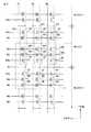
図3は、メモリセルアレイ領域100及び周辺回路領域200の平面構造を図示している。図4は、図3に示されるA−A線、B−B線及びC−C線に沿う断面構造を図示している。また、図5及び図6は、図3のD−D線に沿うメモリセルアレイ領域100の断面構造の一例をそれぞれ図示している。 FIG. 3 illustrates a planar structure of the memory
図3に示すように、メモリセルアレイ領域100の表面領域は、複数のアクティブ領域AAと複数の素子分離領域STIから構成されている。アクティブ領域AA及び素子分離領域STIはY方向に延在し、1つのアクティブ領域AAは2つの素子分離領域STIに挟み込まれている。 As shown in FIG. 3, the surface region of the memory
複数のワード線WLはX方向に延在し、アクティブ領域AAと交差している。複数のメモリセルMCは、ワード線WLとアクティブ領域AAとの交差箇所にそれぞれ設けられている。セレクトゲート線SGLもワード線WLと同様にX方向に延び、セレクトゲートトランジスタSTはセレクトゲート線SGLとアクティブ領域AAとの交差箇所にそれぞれ設けられている。また、2つのセレクトゲート線間のアクティブ領域AA内には、コンタクトC1が設けられ、これは2つのセレクトゲートトランジスタSTで共有される。 The plurality of word lines WL extend in the X direction and intersect the active area AA. The plurality of memory cells MC are provided at intersections between the word lines WL and the active areas AA. Similarly to the word line WL, the select gate line SGL extends in the X direction, and the select gate transistor ST is provided at each intersection of the select gate line SGL and the active area AA. A contact C1 is provided in the active area AA between the two select gate lines, and is shared by the two select gate transistors ST.
以下、本実施形態においては、メモリセルアレイ領域100のうち、メモリセルが配置(形成)される領域をメモリセル形成領域101と呼び、セレクトゲートトランジスタが配置(形成)される領域をセレクトゲート形成領域と呼ぶ。 Hereinafter, in the present embodiment, in the memory
また、周辺回路領域200内には、高耐圧系MISトランジスタHVTrと低耐圧系MISトランジスタLVTrとが設けられている。以下、本実施形態において、周辺回路領域200のうち、高耐圧系MISトランジスタが配置(形成)される領域を高耐圧系トランジスタ形成領域201と呼び、低耐圧系MISトランジスタが配置(形成)される領域を低耐圧系トランジスタ形成領域202と呼ぶ。高耐圧系及び低耐圧系トランジスタ形成領域201,202はそれぞれ素子分離領域に取り囲まれ、互いに電気的に分離された素子領域AAL,AAHが設けられる。各MISトランジスタHVTr,LVTrのゲート電極7C,7Dは素子領域AAL,AAHを縦断するようにX方向に延び、素子分離領域STI上まで引き出されている。その引き出された箇所において、コンタクト12B,12Cがゲート電極7C,7D上にそれぞれ設けられている。 In the
図4に示すように、メモリセル形成領域101内に設けられるメモリセルMCは、MONOS構造のメモリセルである。即ち、メモリセルMCのゲート構造は、半導体基板1表面上のゲート絶縁膜3A上に電荷蓄積層4Aが設けられ、この電荷蓄積層3Aとゲート電極7Aとの間にブロック絶縁膜6Aが設けられた構造となっている。そして、メモリセルMCは、ソース/ドレイン領域となる2つの拡散層8Aを有し、それをY方向(チャネル長方向)に隣接するメモリセルMCで共有することによって、Y方向に直列接続されている。 As shown in FIG. 4, the memory cell MC provided in the memory
ゲート絶縁膜(第1のゲート絶縁膜)3Aは、例えば、膜厚が4nm程度のシリコン酸化膜であり、電荷蓄積層3Aへの電荷注入の際にトンネル絶縁膜として機能する。また、ゲート絶縁膜3Aに、シリコン酸化膜/シリコン窒化膜/シリコン酸化膜の積層構造を有するONO膜や、ゲート絶縁膜3A中にゲルマニウム(Ge)等の注入アシスト準位を含む層をトンネル膜の両界面に位置させた膜を用いることにより、ゲート絶縁膜の信頼性を向上でき、さらには、書き込み/消去特性を向上できる。 The gate insulating film (first gate insulating film) 3A is, for example, a silicon oxide film having a film thickness of about 4 nm, and functions as a tunnel insulating film at the time of charge injection into the
電荷蓄積層4Aは電荷捕獲準位を多く含む膜であり、例えば、シリコン窒化膜などの絶縁膜である。電荷蓄積層4Aがシリコン窒化膜である場合、その膜厚は3nm〜6nm程度である。電荷蓄積層4Aは、例えば、図5或いは図6に示すように、X方向(チャネル幅方向)において、素子分離領域STI内に埋め込まれた素子分離絶縁膜10によって、電気的に分離されている。尚、電荷蓄積層4AのX方向の断面構造は、図5及び図6に示す例に限定されるものではない。例えば、電荷蓄積層4Aが絶縁膜であれば、X方向に隣接するメモリセルMC間で分離する必要はなく、電荷蓄積層4Aがアクティブ領域AA上及び素子分離領域STI上をX方向に延在する構造であってもよい。 The
ブロック絶縁膜(第1の中間絶縁膜)6Aは、ゲート電極に電圧が印加された際に、電荷蓄積層3Aに捕獲された電荷がゲート電極7Aに放出されるのを阻止する。ブロック絶縁膜6Aは、例えば、Al2O3、HfO2、Ta2O5、La2O3、LaLiO3、ZrO2、Y2O3、ZrSiO4などの高誘電体膜である。さらには、これらの複合膜や、これらの膜とSiN膜又はSiO2膜との積層膜でも良い。ブロック絶縁膜6Aがアルミナ膜である場合、その膜厚は、例えば、20nm〜30nm程度である。ブロック絶縁膜6Aは、図5に示すように素子分離絶縁膜10によって、X方向に隣接するメモリセルMC毎に分離されてもよいし、図6に示すように、電荷蓄積層3A上及び素子分離絶縁膜10上をX方向に延在していてもよい。以下では、アルミナ膜をブロック絶縁膜6Aとして用いた例について説明する。但し、本実施形態は、それに限定されるものではない。The block insulating film (first intermediate insulating film) 6A prevents the charge trapped in the
ゲート電極(第1のゲート電極)7AはX方向に延在し、X方向に隣接する複数のメモリセルMCで共有され、ワード線WLとして機能する。ゲート電極7Aは、例えば、ポリシリコン、シリサイド、アルミ(Al)や銅(Cu)などのメタル材から構成される。また、ゲート電極7Aは上記の材料の単層膜でもよいし、例えば、ポリシリコン上にシリサイドが積層された、いわゆる、ポリサイド膜のように、異なる材料が積層された積層膜でもよい。 The gate electrode (first gate electrode) 7A extends in the X direction, is shared by a plurality of memory cells MC adjacent in the X direction, and functions as a word line WL. The
セレクトゲート形成領域102内に設けられるセレクトゲートトランジスタSTは、次のような構成を有している。セレクトゲートトランジスタSTのゲート構造は、半導体基板1表面上のゲート絶縁膜5Aと、ゲート電極7Bと、ゲート絶縁膜5Aとゲート電極7Bとの間に挟み込まれた中間絶縁膜6Bから構成される。また、セレクトゲートトランジスタSTは、半導体基板1内に設けられた拡散層8B,8Cをソース/ドレイン領域としている。拡散層8Bは、Y方向に隣接するメモリセルMCと共有され、それによってメモリセルMCと直列接続される。拡散層8Cはコンタクト12Aを介して配線層13Aに接続される。 The select gate transistor ST provided in the select
セレクトゲートトランジスタSTのゲート絶縁膜5Aの膜厚は、メモリセルのゲート絶縁膜(トンネル絶縁膜)3Aの膜厚より厚く、例えば、7nm程度である。ゲート絶縁膜5Aの膜厚をゲート絶縁膜3Aの膜厚より厚くすることによって、セレクトゲートトランジスタSTのゲート耐圧が確保されている。また、セレクトゲートトランジスタSTのゲート長は、ドレイン−ソース間耐圧の確保のため、メモリセルMCのゲート長よりも大きくされている。 The film thickness of the
中間絶縁膜(第2の中間絶縁膜)6Bはゲート絶縁膜5A上に設けられている。中間絶縁膜6Bは、メモリセルMCのブロック絶縁膜6Aと同時に形成されるため、ブロック絶縁膜6Bと同一構成であり、例えば、20nm〜30nm程度のアルミナ膜である。 The intermediate insulating film (second intermediate insulating film) 6B is provided on the
ゲート電極(第2のゲート電極)7BはX方向に延在し、X方向に隣接する複数のセレクトゲートトランジスタSTで共有され、セレクトゲート線SGLとして機能する。ゲート電極7Bは、ゲート電極7Aと同時に形成されるため、ゲート電極7Aと同一の構成となる。 The gate electrode (second gate electrode) 7B extends in the X direction, is shared by a plurality of select gate transistors ST adjacent in the X direction, and functions as a select gate line SGL. Since the
高耐圧系トランジスタ形成領域201内に設けられる高耐圧系MISトランジスタHVTrは、次のような構成を有している。高耐圧系MISトランジスタHVTrのゲート構造は、半導体基板1表面上のゲート絶縁膜2と、ゲート電極7Dと、ゲート絶縁膜2とゲート電極7Dとの間に挟み込まれた中間絶縁膜6Dからなる。また、高耐圧系MISトランジスタHVTrは、半導体基板1内に設けられた2つの拡散層8Eをソース/ドレイン領域とし、拡散層8Eはコンタクトを介して、配線層13Cに接続されている。 The high breakdown voltage MIS transistor HVTr provided in the high breakdown voltage
高耐圧系MISトランジスタHVTrは、例えば、書き込み電圧などの高電圧の転送を担う。そのため、そのゲート絶縁膜2の膜厚は、セレクトゲートトランジスタSTのゲート絶縁膜5Bの膜厚よりもさらに厚くされ、それによって、高耐圧系MISトランジスタHVTrのゲート耐圧が確保されている。例えば、ゲート絶縁膜2の膜厚は、30nm以上、50nm以下程度である。 The high voltage MIS transistor HVTr is responsible for transferring a high voltage such as a write voltage, for example. Therefore, the film thickness of the
高耐圧系MISトランジスタHVTrにおいても、セレクトゲートトランジスタSTと同様に、ゲート絶縁膜(第3のゲート絶縁膜)2と中間絶縁膜(第3の中間絶縁膜)6Dとが直接接触した構造となっている。中間絶縁膜6Dもブロック絶縁膜6Aと同一構成であり、例えば、アルミナ膜である。 Similarly to the select gate transistor ST, the high voltage MIS transistor HVTr has a structure in which the gate insulating film (third gate insulating film) 2 and the intermediate insulating film (third intermediate insulating film) 6D are in direct contact with each other. ing. The intermediate
また、ゲート電極(第3のゲート電極)7Dはゲート電極7Aと同時に形成されるため、ゲート電極7Aと同一の構成となる。高耐圧系MISトランジスタHVTrのゲート長は、ドレイン−ソース間耐圧の確保のため、セレクトゲートトランジスタSTやメモリセルMCのゲート長よりも大きくされている。 Further, since the gate electrode (third gate electrode) 7D is formed at the same time as the
低耐圧系トランジスタ形成領域202内に設けられる低耐圧系MISトランジスタLVTrは、高耐圧系MISトランジスタと、ほぼ同一の構成を有している。即ち、低耐圧系MISトランジスタLVTrのゲート構造は、半導体基板1表面上のゲート絶縁膜5Bと、ゲート電極7Cと、ゲート絶縁膜5Bとゲート電極7Dとの間に挟み込まれた中間絶縁膜6Dからなる。そして、低耐圧系MISトランジスタLVTrは、ソース/ドレイン領域として機能する2つの拡散層8Dを半導体基板1内に有しており、拡散層8Dはコンタクト12Bを介して配線層13Bに接続されている。 The low breakdown voltage MIS transistor LVTr provided in the low breakdown voltage
低耐圧系MISトランジスタLVTrのゲート絶縁膜5Bの膜厚は、例えば、6nm〜9nm程度である。中間絶縁膜6Cはブロック絶縁膜6Aと同一構成であり、例えば、アルミナ膜である。また、ゲート電極7Dはゲート電極7Aと同時に形成されるため、ゲート電極7Aと同一の構成となる。
低耐圧系MISトランジスタLVTrは、例えば、ロジック回路のスイッチ素子として機能する。低耐圧系MISトランジスタLVTrのゲート長は、セレクトゲートトランジスタSTや高耐圧系MISトランジスタHVTrと同様に、ドレイン−ソース耐圧の確保のため、メモリセルMCのゲート長よりも大きくされている。The film thickness of the
The low withstand voltage MIS transistor LVTr functions as, for example, a switching element of a logic circuit. The gate length of the low withstand voltage MIS transistor LVTr is set larger than the gate length of the memory cell MC in order to ensure the drain-source withstand voltage, as with the select gate transistor ST and the high withstand voltage MIS transistor HVTr.
本発明の実施形態に係るフラッシュメモリにおいて、メモリセルアレイ領域100内に設けられるセレクトゲートトランジスタSTは、中間絶縁膜6Bとゲート絶縁膜5Aとが直接接触したゲート構造を有している。 In the flash memory according to the embodiment of the present invention, the select gate transistor ST provided in the memory
つまり、本実施形態では、メモリセルMCにおいては、ゲート絶縁膜3Aとゲート電極7Aとの間に、電荷蓄積層4Aとブロック絶縁膜6Aとが介在しているのに対し、セレクトゲートトランジスタSTでは、電荷蓄積層が設けられず、ブロック絶縁膜6Aと同一構成の中間絶縁膜6Bがゲート絶縁膜5Aとゲート電極7Bとの間に介在するのみである。それゆえ、セレクトゲートトランジスタSTでは、そのゲート電極7Bに電圧を印加しても、電荷蓄積層に電荷が注入されることはない。 That is, in the present embodiment, in the memory cell MC, the
したがって、セレクトゲートトランジスタSTにおいて、電荷蓄積層の電荷捕獲に起因するしきい値電圧の変動は生じない。 Therefore, in the select gate transistor ST, the threshold voltage does not fluctuate due to charge trapping of the charge storage layer.
上述のようなセレクトゲートトランジスタSTのゲート構造においては、ゲート電極7Bと半導体基板1表面との間に設けられているゲート絶縁膜5Aと中間絶縁膜6Bとが、積層構造のゲート絶縁膜として実質的に機能する。図7は、そのようなゲート構造のセレクトゲートトランジスタ(MISトランジスタ)の動作特性(Vg−Id特性)のシミュレーション結果を示している。図7においては、横軸(Vg[V])はリニアスケールで示され、縦軸(Id[A])はlogスケールで示されている。図7に示す例では、ゲート絶縁膜/ゲート電極のゲート構造となっているMISトランジスタの特性曲線50と、本実施形態のようにゲート絶縁膜/中間絶縁膜/ゲート電極のゲート構造となっているMISトランジスタの特性曲線51とを示している。尚、特性曲線51における中間絶縁膜(例えば、アルミナ膜)の膜厚は、例えば、20nmである。 In the gate structure of the select gate transistor ST as described above, the
図7の特性曲線51に示すように、ゲート絶縁膜とゲート電極との間に中間絶縁膜が介在していても、通常のMISトランジスタ(特性曲線50)とほぼ同様に、スイッチング動作をする。 As shown by the
上述のように、高耐圧系/低耐圧系MISトランジスタHVTr,LVTrも、セレクトゲートトランジスタSTと同様に電荷蓄積層を含まず、ブロック絶縁膜6Aと同一構成の中間絶縁膜6D,6Cがゲート絶縁膜2,5Bに直接接触したゲート構造を有している。そのため、高耐圧系/低耐圧系MISトランジスタHVTr,LVTrについても、セレクトゲートトランジスタSTと同様に効果が得られる。 As described above, the high-breakdown-voltage / low-breakdown-voltage MIS transistors HVTr and LVTr also do not include a charge storage layer like the select gate transistor ST, and the
また、各トランジスタの駆動力やゲート耐圧の確保のため、セレクトゲートトランジスタSTや高耐圧/低耐圧系MISトランジスタHVTr,LVTrのゲート長は、メモリセルのゲート長よりも大きくされている。ドレイン−ソース間耐圧(例えば、パンチスルー耐圧)やゲート耐圧はゲート絶縁膜に加わる電界強度及びゲート絶縁膜の膜厚に依存する。そのため、ゲート絶縁膜の膜厚が薄い場合には、ゲート長をより大きくすることで、ゲート絶縁膜に印加される電界強度を緩和させ、十分なドレイン−ソース間耐圧が確保される。 Further, in order to ensure the driving power and gate breakdown voltage of each transistor, the gate length of the select gate transistor ST and the high breakdown voltage / low breakdown voltage MIS transistors HVTr and LVTr is set larger than the gate length of the memory cell. The drain-source breakdown voltage (for example, punch-through breakdown voltage) and the gate breakdown voltage depend on the electric field strength applied to the gate insulating film and the thickness of the gate insulating film. Therefore, when the thickness of the gate insulating film is small, the electric field strength applied to the gate insulating film is reduced by increasing the gate length, and a sufficient drain-source breakdown voltage is secured.
本実施形態では、ゲート絶縁膜5Aとゲート電極7Bとの間に中間絶縁膜6Bが介在する結果として、中間絶縁膜6Bも、セレクトゲートトランジスタSTのゲート絶縁膜の一部分として機能する。よって、実質的なゲート絶縁膜の膜厚が厚くなるため、ゲート長が小さくてもゲート絶縁膜のゲート耐圧を十分確保できる。そのため、各トランジスタST,HVTr,LVTrのゲート長を小さくでき、その結果として、セレクトゲート形成領域102や高耐圧系/低耐圧系トランジスタ形成領域201,202(周辺回路領域200)のサイズを縮小できる。それゆえ、メモリセル形成領域のサイズを拡大でき、フラッシュメモリの記憶容量の増大に貢献できる。 In the present embodiment, as a result of the intermediate
さらに、本実施形態においては、セレクトゲートトランジスタSTにおいて、ゲート絶縁膜5Aとゲート電極7Bとの間には、ブロック絶縁膜と同時に形成される中間絶縁膜6Bが設けられている。そのため、メモリセルMCのゲートを構成する積層体の高さ(膜厚)は、セレクトゲートトランジスタのゲートを構成する積層体の高さ(膜厚)よりも、メモリセルMCの積層体内に設けられる電荷蓄積層4Aの膜厚分だけ高くなる。電荷蓄積層4A(例えば、シリコン窒化膜)の膜厚は5nm程度であるため、メモリセルMCの積層体(ゲート)の上端とセレクトゲートトランジスタSTの積層体(ゲート)の上端と間に生じる段差も、5nm程度となる。 Further, in the present embodiment, in the select gate transistor ST, an intermediate
セレクトゲート形成領域102内の電荷蓄積層を除去する工程がブロック絶縁膜(中間絶縁膜)形成工程の後に実行された場合、電荷蓄積層とともにブロック絶縁膜も同時に除去される。この場合、セレクトゲートトランジスタSTは、ゲート絶縁膜とゲート電極とが直接接触した構造となり、メモリセルMCのゲート(積層体)の上端とセレクトゲートトランジスタSTのゲート(積層体)の上端と間に生じる段差は、電荷蓄積層とブロック絶縁膜との膜厚分、例えば、25nm〜30nm程度となる。 When the step of removing the charge storage layer in the select
本実施形態のように、ブロック絶縁膜(中間絶縁膜)を除去せず、セレクトゲートトランジスタSTのゲートに残存させることで、メモリセル形成領域101とセレクトゲートト形成領域102との間に生じる段差を小さくできる。したがって、リソグラフィーやエッチングにおいて、段差に起因するプロセスマージンの低下を抑制することができる。 As in the present embodiment, the step insulating film (intermediate insulating film) is not removed and left at the gate of the select gate transistor ST, thereby causing a step between the memory
また、本実施形態のように、メモリセル形成領域101とセレクトゲート形成領域102との間の段差が小さくなれば、CMP(Chemical Mechanical Polishing)法による、段差解消のための平坦化処理を実行せずともよい。それゆえ、製造工程数を減少させることもできる。さらに、本実施形態では、メモリセルMCとセレクトゲートトランジスタSTのゲートとなる積層体の構成の違いは、膜厚の薄い電荷蓄積層の有無だけである。そのため、メモリセルMCとセレクトゲートトランジスタSTのゲート加工を、一度の工程で実行できる。それゆえ、電荷蓄積層とブロック絶縁膜とが両方とも無い積層体と比較して、ゲートの加工が容易となる。 Further, as in this embodiment, when the step between the memory
尚、高耐圧系/低耐圧系MISトランジスタHVTr,LVTrも、セレクトゲートトランジスタSTと同様に、中間絶縁膜6D,6Cがゲートを構成する積層体に設けられている。そのため、高耐圧系/低耐圧系トランジスタ形成領域201,202においても、それらの領域とメモリセル領域101との間の段差や形成された膜の構成の違いが小さくなり、製造工程の削減及び加工難度の低下を図ることができる。 Note that the high-breakdown-voltage / low-breakdown-voltage MIS transistors HVTr and LVTr are also provided in the stacked body in which the intermediate insulating
以上のように、本発明の実施形態に係るフラッシュメモリによれば、その動作の安定化を図ることができる。 As described above, the flash memory according to the embodiment of the present invention can stabilize the operation.
また、本発明の実施形態に係るフラッシュメモリによれば、その製造工程において、加工難度を低減させることができる。 Moreover, according to the flash memory according to the embodiment of the present invention, the processing difficulty can be reduced in the manufacturing process.
(3) 製造方法
以下、図4乃至図10を用いて、本発明の実施形態に係る不揮発性半導体メモリ(フラッシュメモリ)の製造方法について説明する。(3) Manufacturing method
Hereinafter, a method for manufacturing a nonvolatile semiconductor memory (flash memory) according to an embodiment of the present invention will be described with reference to FIGS.
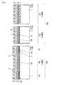
はじめに、図8に示すように、高耐圧系トランジスタ形成領域201内において、例えば、RIE(Reactive Ion Etching)法によって、半導体基板1がエッチングされ、凹部が半導体基板1内に形成される。即ち、高耐圧系トランジスタ形成領域201の半導体基板1表面が、メモリセルアレイ領域100及び低耐圧トランジスタ形成領域202の半導体基板1表面よりも低くなる。 First, as shown in FIG. 8, in the high breakdown voltage
そして、半導体基板1表面に犠牲酸化膜(図示せず)が形成された後、メモリセルアレイ領域100内及び周辺回路領域の高耐圧系/低耐圧系トランジスタ形成領域201,202に対し、例えば、それぞれ異なるドーズ量のイオン注入が実行され、各素子形成領域に対応した不純物濃度のウェル領域(図示せず)がそれぞれ形成される。 Then, after a sacrificial oxide film (not shown) is formed on the surface of the
犠牲酸化膜が剥離された後、半導体基板1に対して、例えば、熱酸化処理が施され、半導体基板1表面に30〜50nm程度の絶縁膜(例えば、シリコン酸化膜)が形成される。このシリコン酸化膜は、例えば、フォトリソグラフィー技術及びRIE法によって、メモリセルアレイ領域100内及び低耐圧系トランジスタ形成領域202内では除去され、高耐圧系トランジスタ形成領域201内の凹部内(半導体基板1表面)にのみ残存される。この高耐圧系トランジスタ形成領域201内に残存したシリコン酸化膜2は、高耐圧系MISトランジスタのゲート絶縁膜となる。尚、各領域間の段差を緩和するため、酸化膜2の上端がメモリセルアレイ領域100の半導体基板1表面上端とほぼ一致するように、凹部が形成されることが好ましい。 After the sacrificial oxide film is peeled off, the
続いて、半導体基板1表面に対し、例えば、熱酸化処理が再び実行され、メモリセルアレイ領域100内及び低耐圧系トランジスタ形成領域202内の半導体基板1表面にシリコン酸化膜3が形成される。シリコン酸化膜3はメモリセルのトンネル絶縁膜となり、その膜厚は、3nm〜5nm程度である。 Subsequently, for example, a thermal oxidation process is performed again on the surface of the
そして、メモリセルの電荷蓄積層となる絶縁材(以下、電荷蓄積層材と呼ぶ)4が、例えば、CVD(Chemical Vapor Deposition)法により、4nm〜6nm程度の膜厚で、シリコン酸化膜2,3上に形成される。電荷蓄積層材4は、例えば、シリコン窒化膜など、電荷捕獲準位を多く含む材料から構成される。 An insulating material 4 (hereinafter referred to as a charge storage layer material) 4 serving as a charge storage layer of the memory cell is formed to a thickness of about 4 nm to 6 nm, for example, by a CVD (Chemical Vapor Deposition) method. 3 is formed. The charge
次に、図9に示すように、メモリセルアレイ領域100内のセレクトゲート形成領域102、高耐圧系/低耐圧系トランジスタ形成領域201,202内の電荷蓄積層材4が、例えば、フォトリソグラフィー技術及びRIE法を用いて、除去される。それに加え、例えば、セレクトゲート形成領域102内及び低耐圧系トランジスタ形成領域202内においては、半導体基板1表面のシリコン酸化膜も除去される。そして、新たな絶縁膜(例えば、シリコン酸化膜)5A,5Bが、例えば、熱酸化処理によって膜厚が6nm程度となるように、セレクトゲート形成領域102内及び低耐圧系トランジスタ形成領域202内の半導体基板1表面上に形成される。シリコン酸化膜5A,5Bは、セレクトゲートトランジスタ及び低耐圧系MISトランジスタのゲート絶縁膜となる。 Next, as shown in FIG. 9, the charge
ここで、図3に示すメモリセルのD−D線に沿う断面構造が図6に示す構造の場合には、電荷蓄積層材4の形成後に、フォトリソグラフィー技術及びRIE法により、半導体基板1内に溝が形成される。その溝内に素子分離絶縁膜が埋め込まれ、アクティブ領域と素子分離領域とが形成される。 Here, when the cross-sectional structure along the line D-D of the memory cell shown in FIG. 3 is the structure shown in FIG. 6, after the charge
この工程によって、メモリセル形成領域101内には、電荷蓄積層材4がメモリセルのゲート絶縁膜3A上に残存し、セレクトゲート形成領域102内においては、電荷蓄積層材4は存在せず、選択トランジスタのゲート絶縁膜となるシリコン酸化膜5Aの表面が露出した構造となる。また、周辺回路領域200内においても、電荷蓄積層材4が存在せず、高耐圧系/低耐圧系MISトランジスタのゲート絶縁膜となるシリコン酸化膜2,5B表面が露出した構造となる。 By this step, the charge
続いて、図10に示すように、メモリセルアレイ領域100内及び周辺トランジスタ領域200内において、メモリセルのブロック絶縁膜となる絶縁材6が、例えば、CVD法によって、20nm〜30nm程度の膜厚となるように、電荷蓄積層材4及び絶縁膜5A,5B上に形成される。絶縁材6は、例えば、アルミナ(Al2O3)である。尚、それに限定されず、酸化ハフニウムなど他の高誘電体絶縁材料や、シリコン窒化膜、シリコン酸化膜などの絶縁膜でもよい。Subsequently, as shown in FIG. 10, in the memory
また、絶縁膜6上には、ゲート電極材7が形成され、さらに、ゲート電極材7上に、ゲート形成工程の際のマスクとなるマスク材9が形成される。ゲート電極材7は、例えば、ポリシリコン膜、シリサイド膜、或いは、タングステン(W)やアルミ(Al)、銅(Cu)等のメタル材などのうち、いずれか1つが用いられる。また、その構造は、それらのゲート電極材の単層膜でもよいし、例えば、ポリサイド構造のように、ポリシリコン膜とシリサイド膜とが積層された積層膜でもよい。 A
メモリセル及び各トランジスタのゲート電極をポリサイド構造とする場合には、以下の順序で形成される。絶縁膜6上に、ポリシリコン膜が例えばCVD法により形成され、そのポリシリコン層上に、例えば、ニッケル(Ni)膜がスパッタ法により形成される。そして、半導体基板1に加熱処理を施して、ポリシリコン膜の上部をNi膜とシリサイド反応させる。これによって、ポリシリコン膜上にニッケルシリサイド(NiSi2)膜が形成され、ポリサイド構造のゲート電極材が形成される。ゲート電極をシリサイド膜の単層構造、いわゆるFUSI構造とする場合には、上記のシリサイド処理工程において、ポリシリコン膜の全体をシリサイド化させる。また、ゲート電極をポリシリコン膜又はメタル膜の単層構造とする場合には、CVD法又はスパッタ法により、ゲート電極材7が絶縁膜6上に形成される。When the memory cell and the gate electrode of each transistor have a polycide structure, they are formed in the following order. A polysilicon film is formed on the insulating
この工程により、メモリセル形成領域101内においては、ゲート絶縁膜となる絶縁膜3Aとブロック絶縁膜となる絶縁膜6との間に、電荷蓄積層となる電荷蓄積層材4が介在した構造となる。一方、セレクトゲート形成領域102内、高耐圧/低耐圧系トランジスタ形成領域201,202内においては、ゲート絶縁膜となる絶縁膜2,5A,5Bと絶縁膜6との間には、電荷蓄積層材は存在せず、絶縁膜5A,5B,2と絶縁膜6とが直接接触した構造となる。 With this process, in the memory
この場合、メモリセル形成領域100とセレクトゲート形成領域102とにおいて、段差Zが生じている。この段差Zは、セレクトゲート形成領域102内に電荷蓄積層材4が含まれていないことに起因し、その領域102内で積層された膜(以下、積層体と呼ぶ)上端が、メモリセル形成領域101内の積層体上端よりも、電荷蓄積層材4の膜厚(例えば、5nm程度)分、半導体基板1側に後退している。尚、周辺回路領域200内においても、その領域の積層体上端は、メモリセル形成領域101の積層体上端より、電荷蓄積層材4の膜厚程度、半導体基板1側に後退している
続いて、図4に示すように、メモリセルMC、セレクトゲートトランジスタST、高耐圧系/低耐圧系MISトランジスタHVTr,LVTrがそれぞれ所定のパターンのゲートサイズとなるように、フォトリソグラフィー技術によって、パターニングされる。そのパターンに基づいて、ゲート電極材7、絶縁材6及び電荷蓄積層材4が、例えば、RIE法により順次エッチングされる。メモリセルMC、セレクトゲートトランジスタST及び高耐圧/低耐圧系MISトランジスタHVTr,LVTrのゲートとなる積層体が形成される。In this case, a step Z is generated between the memory
そして、それらの積層体をマスクとして、ソース/ドレイン領域となる拡散層8A,8B,8C,8D,8Eが、積層体に対して自己整合的に半導体基板1内に形成される。これによって、メモリセルMC、セレクトゲートトランジスタST、高耐圧系/低耐圧系MISトランジスタHVTr,LVTrが、メモリセルアレイ領域100及び周辺回路領域200にそれぞれ形成される。 Then, using these stacked bodies as masks, diffusion layers 8A, 8B, 8C, 8D, and 8E serving as source / drain regions are formed in the
その後、絶縁層11が、メモリセルMC、各トランジスタST,HVTr,LVTrのゲートを覆うように、例えばCVD法によって形成される。そして、絶縁層11に対して平坦化処理が実行された後、メモリセルアレイ領域100及び周辺回路200のコンタクト形成領域内において、コンタクト12A,12B,12Cが、拡散層8C,8D,8Eに直接接触するように絶縁層11内に埋め込まれる。さらに、配線層13A,13B,13Cが、コンタクト12A,12B,12Cと接続されるように、絶縁層11上に形成される。 Thereafter, the insulating
以上の製造工程によって、本発明の実施形態に係るフラッシュメモリが完成する。 The flash memory according to the embodiment of the present invention is completed by the above manufacturing process.
本発明の実施形態の製造方法において、メモリセルアレイ領域100内のセレクトゲート形成領域102内に形成された電荷蓄積層材が除去される。そして、その領域102内においては、ゲート絶縁膜5A上に直接接触するように、ブロック絶縁膜となる絶縁材6が形成される。 In the manufacturing method according to the embodiment of the present invention, the charge storage layer material formed in the select
それゆえ、上述の製造工程によって形成されるセレクトゲートトランジスタSTは、そのゲート内に電荷蓄積層を含まず、ブロック絶縁膜6Aと同時に形成される中間絶縁膜6Bがゲート絶縁膜5Aと直接接触した構成となる。それゆえ、本実施形態の製造方法によれば、電荷蓄積層に起因するしきい値変動が生じないセレクトゲートトランジスタを提供できる。 Therefore, the select gate transistor ST formed by the above manufacturing process does not include a charge storage layer in the gate, and the intermediate
また、従来のフラッシュメモリの製造方法において、セレクトゲートトランジスタSTのしきい値電圧の変動を抑制するために、セレクトゲート形成領域102内の電荷蓄積層材3だけでなく、ブロック絶縁膜となる絶縁材6も除去された場合、図9に示されるメモリセル形成領域101上端とセレクトゲート形成領域102上端との段差Zは、電荷蓄積層3Aと絶縁材6Bとの膜厚程度、例えば、25nm〜30nm程度になる。この場合、段差に起因して、メモリセル形成領域101とセレクトゲート形成領域102とでリソグラフィーの解像度に差異が生じ、プロセスマージンが低下してしまう。 In the conventional flash memory manufacturing method, not only the charge
一方、本発明の実施形態に係るフラッシュメモリの製造方法では、セレクトゲート形成領域102内に絶縁材6が残存されているため、段差Zは電荷蓄積層材3の膜厚(例えば、5nm)程度である。したがって、本実施形態によれば、段差Zを小さくでき、プロセスマージンの低下を抑制できる。 On the other hand, in the flash memory manufacturing method according to the embodiment of the present invention, since the insulating
また、上記のような25nm〜30nm程度の段差を解消するために、平坦化処理のためCMP法を実行する場合、マスク材9上に、ストッパ膜及び犠牲層を形成する工程が増える。また、段差Zによって落ち込んだ部分に、ストッパ膜・犠牲膜が残存し、それを除去する工程も必要になる。
しかし、本実施形態の製造方法では、段差Zが小さいため、ゲート電極材7の形成後に段差を解消するための平坦化処理を実行せずとも良くなる。それゆえ、フラッシュメモリの製造工程を減少できる。In addition, when the CMP method is executed for the planarization process in order to eliminate the step of about 25 nm to 30 nm as described above, a process of forming a stopper film and a sacrificial layer on the mask material 9 is increased. Further, the stopper film / sacrificial film remains in the portion that has fallen due to the step Z, and a process of removing it is also necessary.
However, in the manufacturing method of the present embodiment, since the step Z is small, it is not necessary to perform a planarization process for eliminating the step after forming the
さらに、従来のように、セレクトゲート形成領域102内の電荷蓄積層材3及び絶縁材6を除去した場合では、ゲート形成工程において、メモリセル形成領域101内とセレクトゲート形成領域102内とで、ゲートとなる積層体の構成が異なる。そのため、その2つの領域101,102に対して共通のエッチング選択比を確保することが困難となり、メモリセル及びセレクトゲートトランジスタのゲートを、同時にエッチングして形成することは困難であった。
しかし、本実施形態の製造方法では、メモリセル形成領域101とセレクトゲート形成領域102との構成の差異は、膜厚の薄い電荷蓄積層材3の有無のみであるため、ゲート加工の難度を低下させることができる。Further, when the charge
However, in the manufacturing method according to the present embodiment, the difference in configuration between the memory
高耐圧系/低耐圧系トランジスタ形成領域201,202内においても、セレクトゲート形成領域101内と同様に、電荷蓄積層材は除去され、ゲート絶縁膜2,5Bと絶縁材6とが、直接接触するように形成される。それゆえ、本実施形態の製造方法によれば、高耐圧系/低耐圧系トランジスタ形成領域201,202内に対しても、セレクトゲートトランジスタ102に対する効果と同様の効果が得られる。 Also in the high breakdown voltage / low breakdown voltage
以上のように、本発明の実施形態に係るフラッシュメモリの製造方法によれば、動作の安定化が図られたフラッシュメモリを提供できる。 As described above, according to the flash memory manufacturing method according to the embodiment of the present invention, it is possible to provide a flash memory whose operation is stabilized.
また、本発明の実施形態に係るフラッシュメモリの製造方法によれば、加工難度を低下させることができる。 Moreover, according to the method for manufacturing a flash memory according to the embodiment of the present invention, the processing difficulty can be reduced.
(4) 変形例
以下、図11及び図12を用いて、上述のフラッシュメモリの構造の変形例、及び、フラッシュメモリの製造方法の変形例について、説明する。(4) Modification
Hereinafter, a modification of the structure of the flash memory and a modification of the method for manufacturing the flash memory will be described with reference to FIGS.
(4−1) 変形例1
図11は、本発明の実施形態に係るフラッシュメモリの変形例について、説明する。(4-1)
FIG. 11 illustrates a modification of the flash memory according to the embodiment of the present invention.
図11に示すように、メモリセルMCのゲート電極7Aの上端とセレクトゲートトランジスタSTのゲート電極7Bの上端が一致している。この構造によれば、メモリセル形成領域101上端とセレクトゲート形成領域102上端との段差が、ほぼ0となる。 As shown in FIG. 11, the upper end of the
このような構造は、ゲート絶縁膜5A表面とゲート絶縁膜3A表面との段差をd1、電荷蓄積層4Aの膜厚をd2とした場合に、d1=d2の関係となるように、各膜3A,4A,5Aを形成すればよい。 In such a structure, when the level difference between the surface of the
具体的な例としては、ゲート絶縁膜3Aの下面とゲート絶縁膜5Aの下面が一致している場合おいて、例えば、ゲート絶縁膜3Aの膜厚が4nm、ゲート絶縁膜5Aの膜厚が8nm、電荷蓄積層4Aの膜厚が4nmとなるように、それぞれ形成する。これによれば、d1=4nm、d2=4nmとなり、d1=d2の関係が成立する。 As a specific example, when the lower surface of the
この結果、メモリセル形成領域101上端とセレクトゲート形成領域102上端との間に段差が生じず、ストッパ膜や犠牲酸化膜が段差に残存することが無くなる。 As a result, no step is formed between the upper end of the memory
(4−2) 変形例2
図12を用いて、本発明の実施形態に係るフラッシュメモリの製造方法の変形例について、説明する。(4-2)
A modification of the method for manufacturing a flash memory according to the embodiment of the present invention will be described with reference to FIG.
はじめに、図8と同様の工程で、各素子形成領域100,201,202内に、ゲート絶縁膜2,3が形成され、そのゲート絶縁膜2,3上に、電荷蓄積層材4が形成される。 First, the
そして、図12に示すように、例えば、フォトリソグラフィー技術及びRIE法によって、セレクトゲート形成領域102内及び高耐圧系/低耐圧系トランジスタ形成領域201,202内の電荷蓄積層4が除去される。
この工程によって、メモリセルアレイ形成領域101内には、電荷蓄積層材4がゲート絶縁膜3上に残存し、セレクトゲート形成領域102内においては、電荷蓄積材4が存在せず、絶縁膜3表面が露出した構造となる。同様に、周辺回路領域200内においても、電荷蓄積層材4は存在せず、低耐圧系/高耐圧系MISトランジスタのゲート絶縁膜となる絶縁膜2,3表面が、それぞれ露出した構造となる。Then, as shown in FIG. 12, the
By this step, the charge
その後、本変形例においては、セレクトゲート形成領域102内の絶縁膜3は除去されず、図10に示す工程と同様の工程によって、その絶縁膜3上に、ブロック絶縁膜となる絶縁材6が形成される。それと同様に、低耐圧系トランジスタ形成領域202内においても、絶縁膜3は除去されず、その絶縁膜3上に絶縁材6が形成される。 Thereafter, in this modification, the insulating
以下、図10に示す工程と同様に、絶縁材6上に、ゲート電極材7が形成され、メモリセルMC、セレクトゲートトランジスタST、低耐圧系/高耐圧系MISトランジスタLVTr,HVTrがそれぞれ形成される。 Thereafter, similarly to the process shown in FIG. 10, the
本変形例に示されるフラッシュメモリの製造方法によれば、メモリセルMCのゲート絶縁膜(トンネル酸化膜)と同じ構成の絶縁膜3が、セレクトゲートトランジスタST及び低耐圧系MISトランジスタLVTrのゲート絶縁膜となる。上述のように、本発明の実施形態によれば、ブロック絶縁膜と同一構成の中間絶縁膜6B,6Cも実質的にゲート絶縁膜の一部となるため、絶縁膜3が薄くとも、セレクトゲートトランジスタST及び低耐圧系MISトランジスタLVTrの機能に問題は生じない。 According to the method of manufacturing the flash memory shown in this modification, the insulating
したがって、本変形例で述べたフラッシュメモリの製造方法によれば、セレクトゲート形成領域102及び周辺トランジスタ形成領域202において、メモリセルMCのゲート絶縁膜を除去する工程と、その後に新たなゲート絶縁膜を形成する工程とを削減することができる。 Therefore, according to the method for manufacturing the flash memory described in this modification, the step of removing the gate insulating film of the memory cell MC in the select
(4−3) 変形例3
以下、変形例3として、図3に示すメモリセルのD−D線に沿う断面構造が図5に示す構造である場合のフラッシュメモリの製造方法について、説明する。尚、本変形例に示す製造工程は、D−D線に沿う断面に対する加工以外は、上述の実施形態で述べた図8から図9までに示される製造工程と同様であるため、ここでの説明は省略する。(4-3)
Hereinafter, as a third modification, a method for manufacturing a flash memory in the case where the cross-sectional structure along the line D-D of the memory cell shown in FIG. In addition, since the manufacturing process shown in this modification is the same as the manufacturing process shown in FIGS. 8 to 9 described in the above-described embodiment except for the processing for the cross section along the line DD, Description is omitted.
メモリセルアレイ領域100内及び周辺トランジスタ領域200内において、メモリセルのブロック絶縁膜となる絶縁材6が、例えば、CVD法によって、20nm〜30nm程度の膜厚となるように、電荷蓄積材4及び絶縁膜5A,5B上に形成される。絶縁材6は、例えば、アルミナ(Al2O3)である。尚、それに限定されず、酸化ハフニウムなど他の高誘電体絶縁材料や、シリコン窒化膜、シリコン酸化膜などの絶縁膜でもよい。In the memory
ブロック絶縁膜となる絶縁膜6が形成された後、フォトリソグラフィー技術及びRIE法により、半導体基板1内に溝が形成される。その溝内に素子分離絶縁膜10が埋め込まれ、アクティブ領域と素子分離領域とが形成される。その後、ゲート電極材7が絶縁膜6上及び素子分離絶縁膜10上に形成される。 After the insulating
この工程により、メモリセル形成領域101内においては、ゲート絶縁膜となる絶縁膜3Aとブロック絶縁膜となる絶縁膜6との間に、電荷蓄積層となる電荷蓄積層材4が介在した構造となる。一方、セレクトゲート形成領域102内、高耐圧系/低耐圧系トランジスタ形成領域201,202内においては、ゲート絶縁膜2,5A,5Bと絶縁膜6との間には、電荷蓄積層材が存在せず、絶縁膜2,5A,5Bと絶縁膜6とが直接接触した構造となる。この後、図4に示される製造工程と同様の工程で、各トランジスタのゲート電極及びソース/ドレインとなる拡散層が形成され、本変形例に係るフラッシュメモリが完成する。 With this process, in the memory
本発明の実施形態の変形例3に係るフラッシュメモリの製造方法においても、本発明の実施形態と同様の効果が得られる。 In the flash memory manufacturing method according to the third modification of the embodiment of the present invention, the same effect as that of the embodiment of the present invention can be obtained.
3. その他
本発明の例によれば、不揮発性半導体メモリの動作の安定化を図ることができる。3. Other
According to the example of the present invention, the operation of the nonvolatile semiconductor memory can be stabilized.
本発明の実施形態においては、NAND型の回路構成のメモリセルアレイを例に説明したが、それに限定されるものではなく、NOR型、AND型など他の回路構成でもよい。 In the embodiments of the present invention, a memory cell array having a NAND type circuit configuration has been described as an example. However, the present invention is not limited to this, and other circuit configurations such as a NOR type and an AND type may be used.
本発明の例は、上述の実施形態に限定されるものではなく、その要旨を逸脱しない範囲で、各構成要素を変形して具体化できる。また、上述の実施形態に開示されている複数の構成要素の適宜な組み合せにより種々の発明を構成できる。例えば、上述の実施形態に開示される全構成要素から幾つかの構成要素を削除してもよいし、異なる実施形態の構成要素を適宜組み合わせてもよい。 The example of the present invention is not limited to the above-described embodiment, and can be embodied by modifying each component without departing from the gist thereof. Various inventions can be configured by appropriately combining a plurality of constituent elements disclosed in the above-described embodiments. For example, some constituent elements may be deleted from all the constituent elements disclosed in the above-described embodiments, or constituent elements of different embodiments may be appropriately combined.
1:半導体基板、2:ゲート絶縁膜、3A:ゲート絶縁膜(トンネル絶縁膜)、4A:電荷蓄積層、5A,5B:ゲート絶縁膜、6A:ブロック絶縁膜、6B,6C,6D:中間絶縁膜、7A,7B,7C,7D:ゲート電極、8A,8B,8C,8D,8E:ソース/ドレイン拡散層、10:素子分離絶縁膜、11:層間絶縁膜、12A,12B,12C:コンタクト、13A,13B,13C:配線層、4:電荷蓄積層材、6:絶縁材(ブロック絶縁膜、中間絶縁膜)、7:ゲート電極材、9:マスク材、100:メモリセルアレイ領域、101:メモリセル形成領域、102:セレクトゲート形成領域、200:周辺回路領域、201:高耐圧系トランジスタ領域、202:低耐圧系トランジスタ領域、210:ワード線・セレクトゲート線ドライバ、220:センスアンプ回路、230:制御回路。 1: Semiconductor substrate, 2: Gate insulating film, 3A: Gate insulating film (tunnel insulating film), 4A: Charge storage layer, 5A, 5B: Gate insulating film, 6A: Block insulating film, 6B, 6C, 6D: Intermediate insulating Film, 7A, 7B, 7C, 7D: gate electrode, 8A, 8B, 8C, 8D, 8E: source / drain diffusion layer, 10: element isolation insulating film, 11: interlayer insulating film, 12A, 12B, 12C: contact, 13A, 13B, 13C: wiring layer, 4: charge storage layer material, 6: insulating material (block insulating film, intermediate insulating film), 7: gate electrode material, 9: mask material, 100: memory cell array region, 101: memory Cell formation region, 102: Select gate formation region, 200: Peripheral circuit region, 201: High breakdown voltage transistor region, 202: Low breakdown voltage transistor region, 210: Word line / selection region DOO line driver, 220: a sense amplifier circuit, 230: control circuit.
Claims (5)
Translated fromJapanese前記メモリセルアレイ領域内に設けられるメモリセル形成領域及びセレクトゲート形成領域と、
前記メモリセル形成領域内の半導体基板内に設けられる2つの第1の拡散層と、前記第1の拡散層間の前記半導体基板表面に設けられる第1のゲート絶縁膜と、前記第1のゲート絶縁膜上に設けられる電荷蓄積層と、前記電荷蓄積層上に設けられブロック絶縁膜となる第1の中間絶縁膜、前記第1の中間絶縁膜上に設けられる第1のゲート電極とをそれぞれ有する複数のメモリセルと、
前記セレクトゲート形成領域内の前記半導体基板内に設けられる2つの第2の拡散層と、前記第2の拡散層間の前記半導体基板表面に設けられる第2のゲート絶縁膜と、前記第2のゲート絶縁膜上に直接接触して設けられる前記第1の中間絶縁膜と同一構成の第2の中間絶縁膜と、前記第2の中間絶縁膜上に設けられる第2のゲート電極とをそれぞれ有する複数のセレクトゲートトランジスタと、
を具備することを特徴とする不揮発性半導体メモリ。A memory cell array region provided in a semiconductor substrate;
A memory cell formation region and a select gate formation region provided in the memory cell array region;
Two first diffusion layers provided in the semiconductor substrate in the memory cell formation region, a first gate insulating film provided on the surface of the semiconductor substrate between the first diffusion layers, and the first gate insulation A charge storage layer provided on the film; a first intermediate insulating film provided on the charge storage layer and serving as a block insulating film; and a first gate electrode provided on the first intermediate insulating film. A plurality of memory cells;
Two second diffusion layers provided in the semiconductor substrate in the select gate formation region, a second gate insulating film provided on the semiconductor substrate surface between the second diffusion layers, and the second gate A plurality of second intermediate insulating films having the same configuration as the first intermediate insulating film provided in direct contact with the insulating film, and a second gate electrode provided on the second intermediate insulating film. Select gate transistors of
A non-volatile semiconductor memory comprising:
前記複数のセレクトゲートトランジスタの前記第2の拡散層は、前記直列接続された複数のメモリセルの一端及び他端の前記第1の拡散層に接続され、
前記直列接続された複数のメモリセルの前記第1のゲート電極上端と前記セレクトゲートトランジスタの前記第2のゲート電極上端とには、段差があることを特徴とする請求項1に記載の不揮発性半導体メモリ。The plurality of memory cells are connected in series so as to share each of the first diffusion layers,
The second diffusion layers of the plurality of select gate transistors are connected to the first diffusion layers at one end and the other end of the plurality of memory cells connected in series,
2. The nonvolatile memory according to claim 1, wherein there is a step between an upper end of the first gate electrode of the plurality of memory cells connected in series and an upper end of the second gate electrode of the select gate transistor. Semiconductor memory.
前記周辺回路領域内の前記半導体基板内に設けられる2つの第3の拡散層と、前記第3の拡散層間の前記半導体基板表面に設けられる第3のゲート絶縁膜と、前記第3のゲート絶縁膜上に直接接触して設けられる前記第1の中間絶縁膜と同一構成の第3の中間絶縁膜と、前記第2の中間絶縁膜上に設けられる第3のゲート電極とそれぞれ有する複数の周辺トランジスタとをさらに具備し、
前記第3のゲート絶縁膜の膜厚は、前記第2のゲート絶縁膜の膜厚よりも厚いことを特徴とする請求項1又は2に記載の不揮発性半導体メモリ。A peripheral circuit region adjacent to the memory cell array region;
Two third diffusion layers provided in the semiconductor substrate in the peripheral circuit region, a third gate insulating film provided on the surface of the semiconductor substrate between the third diffusion layers, and the third gate insulation A plurality of peripherals each having a third intermediate insulating film having the same configuration as the first intermediate insulating film provided in direct contact with the film and a third gate electrode provided on the second intermediate insulating film A transistor,
3. The nonvolatile semiconductor memory according to claim 1, wherein a film thickness of the third gate insulating film is larger than a film thickness of the second gate insulating film.
前記第1のゲート絶縁膜材上に、電荷蓄積層となる電荷蓄積層材を形成する工程と、
前記セレクトゲート形成領域内の前記電荷蓄積層材を除去し、前記セレクトゲート形成領域内の前記第1のゲート絶縁膜材表面を露出させる工程と、
前記セレクトゲート形成領域内の前記第1のゲート絶縁膜材を除去し、前記セレクトゲート形成領域内に第2のゲート絶縁膜材を形成する工程と、
前記メモリセル形成領域内に残存された前記電荷蓄積層上及び前記セレクトゲート形成領域内の前記第2のゲート絶縁膜上に、絶縁材を形成する工程と、
前記絶縁材上に、ゲート電極材を形成する工程と、
前記メモリセル形成領域内の前記ゲート電極材、前記絶縁材及び前記電荷蓄積層材、前記セレクトゲート形成領域内の前記ゲート電極材及び前記絶縁材を順次エッチングすることによって、前記メモリセル形成領域内においては、第1のゲート電極、メモリセルのブロック絶縁膜となる第1の中間絶縁膜及び電荷蓄積層からなる第1の積層体を形成し、前記セレクトゲート形成領域内においては、第2のゲート電極及び前記第1の中間絶縁膜と同一構成の第2の中間絶縁膜からなる第2の積層体を形成する工程と、
前記メモリセル形成領域内及び前記セレクトゲート形成領域内の前記半導体基板内に、前記第1及び第2の積層体に対して自己整合的に、メモリセル及びセレクトゲートトランジスタのソース/ドレイン領域となる第1及び第2の拡散層をそれぞれ形成する工程と、
を具備することを特徴とする不揮発性半導体メモリの製造方法。Forming a first gate insulating film material in a memory cell formation region and a select gate formation region in a memory cell array region in a semiconductor substrate;
Forming a charge storage layer material to be a charge storage layer on the first gate insulating film material;
Removing the charge storage layer material in the select gate formation region to expose the surface of the first gate insulating film material in the select gate formation region;
Removing the first gate insulating film material in the select gate forming region and forming a second gate insulating film material in the select gate forming region;
Forming an insulating material on the charge storage layer remaining in the memory cell forming region and on the second gate insulating film in the select gate forming region;
Forming a gate electrode material on the insulating material;
By sequentially etching the gate electrode material, the insulating material and the charge storage layer material in the memory cell formation region, the gate electrode material and the insulation material in the select gate formation region, the memory cell formation region In the first gate electrode, a first stacked body including a first intermediate insulating film serving as a block insulating film of the memory cell and a charge storage layer is formed, and a second stacked body is formed in the select gate formation region. Forming a second stacked body composed of a gate electrode and a second intermediate insulating film having the same configuration as the first intermediate insulating film;
In the semiconductor substrate in the memory cell formation region and the select gate formation region, the source / drain regions of the memory cell and the select gate transistor become self-aligned with respect to the first and second stacked bodies. Forming each of the first and second diffusion layers;
A method of manufacturing a nonvolatile semiconductor memory, comprising:
前記犠牲膜の上面に対して、平坦化処理を行う工程と、
前記犠牲膜にパターンニングを施して、前記第1及び第2の積層体とを形成する工程と、をさらに具備することを特徴とする請求項4に記載の不揮発性半導体メモリの製造方法。Forming a sacrificial film on the gate electrode material;
Performing a planarization process on the upper surface of the sacrificial film;
The method for manufacturing a nonvolatile semiconductor memory according to claim 4, further comprising: patterning the sacrificial film to form the first and second stacked bodies.
Priority Applications (2)
| Application Number | Priority Date | Filing Date | Title |
|---|---|---|---|
| JP2008048410AJP2009206355A (en) | 2008-02-28 | 2008-02-28 | Nonvolatile semiconductor memory, and method of manufacturing nonvolatile semiconductor memory |
| US12/393,186US7960779B2 (en) | 2008-02-28 | 2009-02-26 | Nonvolatile semiconductor memory and manufacturing method thereof |
Applications Claiming Priority (1)
| Application Number | Priority Date | Filing Date | Title |
|---|---|---|---|
| JP2008048410AJP2009206355A (en) | 2008-02-28 | 2008-02-28 | Nonvolatile semiconductor memory, and method of manufacturing nonvolatile semiconductor memory |
Publications (1)
| Publication Number | Publication Date |
|---|---|
| JP2009206355Atrue JP2009206355A (en) | 2009-09-10 |
Family
ID=41012502
Family Applications (1)
| Application Number | Title | Priority Date | Filing Date |
|---|---|---|---|
| JP2008048410APendingJP2009206355A (en) | 2008-02-28 | 2008-02-28 | Nonvolatile semiconductor memory, and method of manufacturing nonvolatile semiconductor memory |
Country Status (2)
| Country | Link |
|---|---|
| US (1) | US7960779B2 (en) |
| JP (1) | JP2009206355A (en) |
Cited By (1)
| Publication number | Priority date | Publication date | Assignee | Title |
|---|---|---|---|---|
| WO2021020084A1 (en)* | 2019-07-26 | 2021-02-04 | 東京エレクトロン株式会社 | Semiconductor device |
Families Citing this family (3)
| Publication number | Priority date | Publication date | Assignee | Title |
|---|---|---|---|---|
| US8804424B2 (en)* | 2011-08-25 | 2014-08-12 | Micron Technology, Inc. | Memory with three transistor memory cell device |
| US8796751B2 (en) | 2012-11-20 | 2014-08-05 | Micron Technology, Inc. | Transistors, memory cells and semiconductor constructions |
| US8930866B2 (en)* | 2013-03-11 | 2015-01-06 | Taiwan Semiconductor Manufacturing Company, Ltd. | Method of converting between non-volatile memory technologies and system for implementing the method |
Citations (4)
| Publication number | Priority date | Publication date | Assignee | Title |
|---|---|---|---|---|
| JP2002100686A (en)* | 2000-09-21 | 2002-04-05 | Toshiba Corp | Nonvolatile semiconductor memory device and method of manufacturing the same |
| JP2004221589A (en)* | 2003-01-10 | 2004-08-05 | Samsung Electronics Co Ltd | Nonvolatile memory device having charge storage insulating film and method of manufacturing the same |
| JP2005116551A (en)* | 2003-10-02 | 2005-04-28 | Toshiba Corp | Semiconductor memory device and manufacturing method thereof |
| JP2007294935A (en)* | 2006-03-31 | 2007-11-08 | Semiconductor Energy Lab Co Ltd | Nonvolatile semiconductor memory device |
Family Cites Families (15)
| Publication number | Priority date | Publication date | Assignee | Title |
|---|---|---|---|---|
| KR100414211B1 (en) | 2001-03-17 | 2004-01-07 | 삼성전자주식회사 | Non-volatile memory device having a metal-oxide-nitride-oxide-semiconductor gate structure and fabrication method thereof |
| DE10228768A1 (en)* | 2001-06-28 | 2003-01-16 | Samsung Electronics Co Ltd | Non-volatile floating trap storage device comprises a semiconductor substrate, a tunnel insulation layer on the substrate, a charge storage layer, a barrier insulation layer, and a gate electrode |
| KR100437453B1 (en)* | 2002-05-23 | 2004-06-23 | 삼성전자주식회사 | NAND-type non-volatile memory device having SONOS gate structure and method of forming the same |
| JP2004296683A (en) | 2003-03-26 | 2004-10-21 | Seiko Epson Corp | Semiconductor device and method of manufacturing the same |
| JP2005116973A (en) | 2003-10-10 | 2005-04-28 | Seiko Epson Corp | Manufacturing method of semiconductor device |
| KR100578131B1 (en)* | 2003-10-28 | 2006-05-10 | 삼성전자주식회사 | Nonvolatile Memory Device and Formation Method |
| KR100553712B1 (en)* | 2004-05-04 | 2006-02-24 | 삼성전자주식회사 | A nonvolatile memory device having a selection transistor having a recess channel and a method of manufacturing the same |
| US6946349B1 (en) | 2004-08-09 | 2005-09-20 | Chartered Semiconductor Manufacturing Ltd. | Method for integrating a SONOS gate oxide transistor into a logic/analog integrated circuit having several gate oxide thicknesses |
| US7227786B1 (en)* | 2005-07-05 | 2007-06-05 | Mammen Thomas | Location-specific NAND (LS NAND) memory technology and cells |
| TWI260769B (en)* | 2005-08-23 | 2006-08-21 | Ememory Technology Inc | Non-volatile memory and operating method thereof |
| US7244985B2 (en)* | 2005-09-06 | 2007-07-17 | Ememory Technology Inc. | Non-volatile memory array |
| US7341914B2 (en)* | 2006-03-15 | 2008-03-11 | Freescale Semiconductor, Inc. | Method for forming a non-volatile memory and a peripheral device on a semiconductor substrate |
| KR100760633B1 (en)* | 2006-04-26 | 2007-09-20 | 삼성전자주식회사 | Charge trap type nonvolatile memory device and method of forming the same |
| KR100843550B1 (en)* | 2006-11-06 | 2008-07-04 | 삼성전자주식회사 | Nonvolatile Memory Device and Manufacturing Method Thereof |
| US7405972B1 (en)* | 2007-01-22 | 2008-07-29 | Ememory Technology Inc. | Non-volatile memory array |
- 2008
- 2008-02-28JPJP2008048410Apatent/JP2009206355A/enactivePending
- 2009
- 2009-02-26USUS12/393,186patent/US7960779B2/enactiveActive
Patent Citations (4)
| Publication number | Priority date | Publication date | Assignee | Title |
|---|---|---|---|---|
| JP2002100686A (en)* | 2000-09-21 | 2002-04-05 | Toshiba Corp | Nonvolatile semiconductor memory device and method of manufacturing the same |
| JP2004221589A (en)* | 2003-01-10 | 2004-08-05 | Samsung Electronics Co Ltd | Nonvolatile memory device having charge storage insulating film and method of manufacturing the same |
| JP2005116551A (en)* | 2003-10-02 | 2005-04-28 | Toshiba Corp | Semiconductor memory device and manufacturing method thereof |
| JP2007294935A (en)* | 2006-03-31 | 2007-11-08 | Semiconductor Energy Lab Co Ltd | Nonvolatile semiconductor memory device |
Cited By (2)
| Publication number | Priority date | Publication date | Assignee | Title |
|---|---|---|---|---|
| WO2021020084A1 (en)* | 2019-07-26 | 2021-02-04 | 東京エレクトロン株式会社 | Semiconductor device |
| JPWO2021020084A1 (en)* | 2019-07-26 | 2021-02-04 |
Also Published As
| Publication number | Publication date |
|---|---|
| US20090218607A1 (en) | 2009-09-03 |
| US7960779B2 (en) | 2011-06-14 |
Similar Documents
| Publication | Publication Date | Title |
|---|---|---|
| KR101059667B1 (en) | Nonvolatile Semiconductor Memory | |
| JP5651415B2 (en) | Nonvolatile semiconductor memory device and manufacturing method thereof | |
| US8344444B2 (en) | Semiconductor device having a nonvolatile memory cell with a cap insulating film formed over a selection gate electrode | |
| CN107437550B (en) | NVM memory HKMG integrated technology | |
| CN106952920B (en) | Semiconductor device and method for manufacturing the same | |
| CN108878427B (en) | Semiconductor device and method for manufacturing the same | |
| CN107818979B (en) | semiconductor device | |
| JP2009272564A (en) | Semiconductor device and method of manufacturing semiconductor device | |
| KR101038131B1 (en) | Nonvolatile semiconductor memory | |
| US8212303B2 (en) | Nonvolatile semiconductor memory device | |
| JP2013026289A (en) | Nonvolatile semiconductor memory device and method of manufacturing the same | |
| US8072021B2 (en) | Nonvolatile semiconductor memory device | |
| US20160079265A1 (en) | Nonvolatile semiconductor memory device and method of manufacturing the same | |
| JP2018056222A (en) | Semiconductor device and method of manufacturing the same | |
| JP2000286349A (en) | Semiconductor device and manufacture thereof | |
| JP2015167200A (en) | Non-volatile semiconductor storage device | |
| JP2007184620A (en) | Semiconductor device having mask ROM and method for manufacturing the same | |
| US20090230460A1 (en) | Nonvolatile semiconductor memory | |
| US7960779B2 (en) | Nonvolatile semiconductor memory and manufacturing method thereof | |
| JP2010153523A (en) | Manufacturing method of semiconductor device, and semiconductor device | |
| JP5787855B2 (en) | Semiconductor memory device | |
| JP2009010110A (en) | Nonvolatile memory and manufacturing method thereof | |
| JP5132330B2 (en) | Nonvolatile semiconductor memory device and manufacturing method thereof | |
| US7705393B2 (en) | Nonvolatile semiconductor storage device having silicide in control gate electrode | |
| JP2008166415A (en) | Semiconductor device and manufacturing method thereof |
Legal Events
| Date | Code | Title | Description |
|---|---|---|---|
| A621 | Written request for application examination | Free format text:JAPANESE INTERMEDIATE CODE: A621 Effective date:20100224 | |
| A977 | Report on retrieval | Free format text:JAPANESE INTERMEDIATE CODE: A971007 Effective date:20100823 | |
| A131 | Notification of reasons for refusal | Free format text:JAPANESE INTERMEDIATE CODE: A131 Effective date:20100831 | |
| A521 | Request for written amendment filed | Free format text:JAPANESE INTERMEDIATE CODE: A523 Effective date:20101029 | |
| A02 | Decision of refusal | Free format text:JAPANESE INTERMEDIATE CODE: A02 Effective date:20101130 |