JP2009204329A - Circuit board inspecting system and inspection method - Google Patents
Circuit board inspecting system and inspection methodDownload PDFInfo
- Publication number
- JP2009204329A JP2009204329AJP2008044381AJP2008044381AJP2009204329AJP 2009204329 AJP2009204329 AJP 2009204329AJP 2008044381 AJP2008044381 AJP 2008044381AJP 2008044381 AJP2008044381 AJP 2008044381AJP 2009204329 AJP2009204329 AJP 2009204329A
- Authority
- JP
- Japan
- Prior art keywords
- circuit board
- wiring
- short
- tester
- dut
- Prior art date
- Legal status (The legal status is an assumption and is not a legal conclusion. Google has not performed a legal analysis and makes no representation as to the accuracy of the status listed.)
- Pending
Links
Images


Classifications
- G—PHYSICS
- G01—MEASURING; TESTING
- G01R—MEASURING ELECTRIC VARIABLES; MEASURING MAGNETIC VARIABLES
- G01R31/00—Arrangements for testing electric properties; Arrangements for locating electric faults; Arrangements for electrical testing characterised by what is being tested not provided for elsewhere
- G01R31/28—Testing of electronic circuits, e.g. by signal tracer
- G01R31/317—Testing of digital circuits
- G01R31/3181—Functional testing
- G01R31/319—Tester hardware, i.e. output processing circuits
- G01R31/31903—Tester hardware, i.e. output processing circuits tester configuration
- G01R31/31905—Interface with the device under test [DUT], e.g. arrangements between the test head and the DUT, mechanical aspects, fixture
Landscapes
- Engineering & Computer Science (AREA)
- General Engineering & Computer Science (AREA)
- Physics & Mathematics (AREA)
- General Physics & Mathematics (AREA)
- Tests Of Electronic Circuits (AREA)
- Testing Of Short-Circuits, Discontinuities, Leakage, Or Incorrect Line Connections (AREA)
- Testing Of Individual Semiconductor Devices (AREA)
Abstract
Description
Translated fromJapanese本発明は、テスタで被検査デバイスを検査する場合に使用する回路ボードを検査する回路ボード検査システム及び検査方法に関する。 The present invention relates to a circuit board inspection system and an inspection method for inspecting a circuit board used when a device under test is inspected by a tester.
LSI(Large Scale Integration)の多機能化、大規模化、高速化に伴い、LSIの全機能をLSIテスタの機能だけで検証することは難しくなっており、LSIテスタが高価になってきている。そのため、LSIテスタを高機能化するのではなく、LSIテスタとLSI等のDUT(Device Under Test;被検査デバイス)の間にDUTを装着することが可能なDUTボードを用いることで、検査コストの低減が図られている。このようなDUTボードにおいては、LSIテスタとDUTを電気的に接続するDUTボード上にCPU(Central Processing Unit)やメモリといった種々の通信デバイスを搭載し、通信デバイスとDUTを通信させて、DUTの機能を検証する場合が増えている。このような背景により、DUTボードの構成が従来に比べ飛躍的に複雑になる場合がある。なお、通常のDUTボードでは、DUTの信号端子とLSIテスタの信号端子が配線を通じて接続されているだけであり、その接続が正しいか否かは、LSIテスタの測定機能を用いて行われる。 As LSI (Large Scale Integration) has become multi-functional, large-scale, and high-speed, it is difficult to verify all the functions of the LSI only with the functions of the LSI tester, and the LSI tester is becoming expensive. For this reason, instead of enhancing the functionality of the LSI tester, the use of a DUT board in which a DUT can be mounted between the LSI tester and a DUT (Device Under Test) such as an LSI reduces the inspection cost. Reduction is being achieved. In such a DUT board, various communication devices such as a CPU (Central Processing Unit) and a memory are mounted on the DUT board that electrically connects the LSI tester and the DUT, and the communication device and the DUT communicate with each other. More and more cases are verifying functionality. Due to this background, the configuration of the DUT board may be dramatically more complicated than in the past. In a normal DUT board, the signal terminal of the DUT and the signal terminal of the LSI tester are simply connected through wiring, and whether or not the connection is correct is performed using the measurement function of the LSI tester.
しかしながら、種々の通信デバイスを搭載した複雑なDUTボードの場合、通信デバイスが所望の機能を有するか否か、DUTと通信デバイスの間の配線接続が正しいか否かは、通信デバイスの信号端子がLSIテスタの信号端子に接続されていないため、その検証が困難である。 However, in the case of a complex DUT board equipped with various communication devices, whether or not the communication device has a desired function and whether or not the wiring connection between the DUT and the communication device is correct depends on the signal terminal of the communication device. Since it is not connected to the signal terminal of the LSI tester, its verification is difficult.
また、DUTと通信デバイスの間の配線に、LSIテスタの機能を用いて通信デバイスの機能が正しいか否か、2つのデバイスが相互に接続されているか否かを検証するための回路を挿入することは、DUTボードの複雑化、高コスト化を招くことになる。さらに、DUTと通信デバイスの間の通信が高速である場合には、この回路によりDUTと通信デバイスの間の信号波形の劣化を招くため、現実上ほぼ不可能になってきている。 Also, a circuit for verifying whether the function of the communication device is correct using the function of the LSI tester or whether the two devices are connected to each other is inserted into the wiring between the DUT and the communication device. This leads to the complexity and cost increase of the DUT board. Furthermore, when communication between the DUT and the communication device is performed at a high speed, this circuit causes deterioration of the signal waveform between the DUT and the communication device, which is practically impossible.
また、通信デバイス自体が所望の機能を有しているか否かを検証するためには、通信デバイス専用のDUTボードが必要となる場合もあり、高コストの要因となる。 Further, in order to verify whether or not the communication device itself has a desired function, a DUT board dedicated to the communication device may be required, which is a high cost factor.
なお、DUTボードやその検査方法に関する従来技術として、特許文献1では、複数のIC装着用ソケットを有するバーンインボードのテストを行うためのプローブが開示されている。このプローブは、ソケットに装着される被試験用IC搭載用パッケージと同様のパッケージを有しており、パッケージの所定の端子間が導通接続されている。このようなプローブをIC装着用ソケットに装着することで、バーインボードの内部配線の確認、搭載部品の確認を行っている。 As a conventional technique related to a DUT board and its inspection method, Patent Document 1 discloses a probe for testing a burn-in board having a plurality of IC mounting sockets. This probe has a package similar to the IC mounting package to be tested that is mounted in the socket, and a predetermined terminal of the package is conductively connected. By mounting such a probe on the IC mounting socket, the internal wiring of the burn-in board and the mounted components are checked.
また、特許文献2では、プリント基板と半導体集積回路装置の外部端子との接続の検査を容易に行う技術が開示されている。この半導体集積回路装置には、半導体集積回路装置の外部端子と接続する入力端子と出力端子とを内部回路を経由して接続するか、あるいは遮断するかを決定するスイッチング回路が設けられている。このような半導体集積回路装置をプリント基板に実装することにより、簡単な導通テスタを用いて単なる入力端子と出力端子の間の抵抗測定レベルを測定することで、接続検証を行っている。
しかしながら、特許文献1、2に記載の技術では、DUTや通信デバイスの検証を行うことができないとともに、DUTと通信デバイスの間の接続の検証を行うことができず、ボード上の搭載部品(終端抵抗や電源フィルター)の接続の検証を行うことができず、パラメータ測定を行うことができない。 However, the techniques described in
本発明の主な課題は、DUTボード上のDUTや通信デバイスの検証、DUTと通信デバイスの間の接続の検証、DUTボード上の搭載部品の接続の検証、パラメータ測定を行えるようにすることである。 The main object of the present invention is to enable verification of DUT and communication device on the DUT board, verification of connection between the DUT and communication device, verification of connection of mounted components on the DUT board, and parameter measurement. is there.
本発明の第1の視点においては、テスタで被検査デバイスを検査する場合に使用する回路ボードを検査する回路ボード検査システムであって、前記回路ボードは、前記被検査デバイスを着脱可能に装着するソケットが実装されるとともに、1又は複数の通信デバイスが直接又は間接的に実装され、前記被検査デバイスの第1信号端子と前記テスタとを電気的に接続する複数の第1配線を有し、前記被検査デバイスの前記第1信号端子と電気的に接続されない第2信号端子と前記通信デバイスの信号端子とを電気的に接続する複数の第2配線を有し、前記回路ボードを検査する際に前記被検査デバイスの代わりにショート基板が前記ソケットに装着され、前記ショート基板は、前記第1配線と前記第2配線を電気的に接続する短絡配線を有することを特徴とする。 According to a first aspect of the present invention, there is provided a circuit board inspection system for inspecting a circuit board used when a device under test is inspected by a tester, wherein the circuit board detachably mounts the device under test. A socket is mounted, and one or a plurality of communication devices are mounted directly or indirectly, and have a plurality of first wirings that electrically connect the first signal terminal of the device under test and the tester; When inspecting the circuit board having a plurality of second wirings that electrically connect a second signal terminal not electrically connected to the first signal terminal of the device to be inspected and a signal terminal of the communication device A short board is mounted in the socket instead of the device to be inspected, and the short board has a short-circuit wiring for electrically connecting the first wiring and the second wiring. And wherein the door.
本発明の第2の視点においては、テスタで被検査デバイスを検査する場合に使用する回路ボードを検査する回路ボード検査方法であって、前記テスタにて、前記回路ボードに装着されたショート基板のタイプを認識する工程と、前記テスタにて、認識された前記ショート基板のタイプに応じて、前記回路ボードと当該回路ボートに実装された通信デバイスとの電気的接続、又は前記通信デバイスの機能を検証する工程と、を含むことを特徴とする。 According to a second aspect of the present invention, there is provided a circuit board inspection method for inspecting a circuit board used when a device under test is inspected by a tester, wherein a short board mounted on the circuit board is tested by the tester. The step of recognizing the type, and the electrical connection between the circuit board and the communication device mounted on the circuit board, or the function of the communication device, according to the type of the short board recognized by the tester And a step of verifying.
本発明の第3の視点においては、テスタで実行されるプログラムであって、前記回路ボード検査方法の各工程をテスタで実行させることを特徴とする。 According to a third aspect of the present invention, there is provided a program executed by a tester, wherein each step of the circuit board inspection method is executed by the tester.
本発明によれば、回路ボードに実装された種々の部品の論理動作の検証、接続確認、パラメータ確認を、テスタの測定機能を用いて、高速に行うことができる。また、本発明によれば、回路ボード上の検査対象となる配線に検証用回路やテスタ信号端子を付加する必要がなく、テスト動作時の信号劣化を起こさず、特性に影響を与えることがなく、回路ボードの面積のオーバヘッドがない。さらに、本発明によれば、テスタで実行されるプログラムでショート基板が装着されたことや、装着されたショート基板の種類を特定できるため、量産の環境においても、テスタ用のソフトウェアをロードしなおしすることなしに回路ボードの検証が可能となり、量産のスループット低下を招かない。 According to the present invention, verification of logical operations, connection confirmation, and parameter confirmation of various components mounted on a circuit board can be performed at high speed using the measurement function of the tester. Further, according to the present invention, it is not necessary to add a verification circuit or a tester signal terminal to the wiring to be inspected on the circuit board, the signal does not deteriorate during the test operation, and the characteristics are not affected. There is no circuit board area overhead. Furthermore, according to the present invention, since the short board is mounted by a program executed by the tester and the type of the mounted short board can be specified, the tester software is reloaded even in a mass production environment. This makes it possible to verify the circuit board without causing a reduction in mass production throughput.
本発明の実施形態に係る回路ボード検査システムでは、テスタ(図1の60)で被検査デバイスを検査する場合に使用する回路ボード(図1の10)を検査する回路ボード検査システムであって、前記回路ボード(図1の10)は、前記被検査デバイスを着脱可能に装着するソケット(図1の20)が実装されるとともに、1又は複数の通信デバイス(図1の50)が直接又は間接的に実装され、前記被検査デバイスの第1信号端子と前記テスタ(図1の60)とを電気的に接続する複数の第1配線(図1の11、12)を有し、前記被検査デバイスの前記第1信号端子と電気的に接続されない第2信号端子と前記通信デバイス(図1の50)の信号端子(図1の51)とを電気的に接続する複数の第2配線(図1の13、14)を有し、前記回路ボード(図1の10)を検査する際に前記被検査デバイスの代わりにショート基板(図1の30)が前記ソケット(図1の20)に装着され、前記ショート基板(図1の30)は、前記第1配線(図1の11、12)と前記第2配線(図1の13、14)を電気的に接続する短絡配線(図1の33、34)を有する。 The circuit board inspection system according to the embodiment of the present invention is a circuit board inspection system that inspects a circuit board (10 in FIG. 1) used when inspecting a device to be inspected by a tester (60 in FIG. 1). The circuit board (10 in FIG. 1) has a socket (20 in FIG. 1) on which the device to be inspected is detachably mounted, and one or a plurality of communication devices (50 in FIG. 1) are directly or indirectly mounted. And a plurality of first wirings (11 and 12 in FIG. 1) that electrically connect the first signal terminal of the device to be inspected and the tester (60 in FIG. 1). A plurality of second wirings (FIG. 1) electrically connecting a second signal terminal not electrically connected to the first signal terminal of the device and a signal terminal (51 of FIG. 1) of the communication device (50 of FIG. 1). 1 and 13, 14) When inspecting a circuit board (10 in FIG. 1), a short board (30 in FIG. 1) is mounted on the socket (20 in FIG. 1) instead of the device under test, and the short board (30 in FIG. 1). Has a short-circuit wiring (33, 34 in FIG. 1) for electrically connecting the first wiring (11, 12 in FIG. 1) and the second wiring (13, 14 in FIG. 1).
本発明の実施形態に係る回路ボード検査方法では、テスタで被検査デバイスを検査する場合に使用する回路ボードを検査する回路ボード検査方法であって、前記テスタにて、前記回路ボードに装着されたショート基板のタイプを認識する工程(図2のステップA2)と、前記テスタにて、認識された前記ショート基板のタイプに応じて、前記回路ボードと当該回路ボートに実装された通信デバイスとの電気的接続、又は前記通信デバイスの機能を検証する工程(図2のステップA3)と、を含む。 The circuit board inspection method according to the embodiment of the present invention is a circuit board inspection method for inspecting a circuit board used when inspecting a device to be inspected by a tester, and is mounted on the circuit board by the tester. The step of recognizing the type of the short board (step A2 in FIG. 2) and the electrical connection between the circuit board and the communication device mounted on the circuit boat according to the type of the short board recognized by the tester Or verifying the function of the communication device (step A3 in FIG. 2).
本発明の実施例1に係る回路ボード検査システムについて図面を用いて説明する。図1は、本発明の実施例1に係る回路ボード検査システムの構成を示した模式図である。 A circuit board inspection system according to Embodiment 1 of the present invention will be described with reference to the drawings. FIG. 1 is a schematic diagram showing a configuration of a circuit board inspection system according to Embodiment 1 of the present invention.
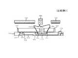
回路ボード検査システムは、回路ボードとなるDUTボード10を検査するシステムであり、ショート基板30(又はDUT;Device Under Test;被検査デバイス)及び通信デバイス50を搭載したDUTボード10とLSIテスタ60が電気的に接続されている。 The circuit board inspection system is a system that inspects a
DUTボード10は、テスト時にショート基板30(又はDUT)及び通信デバイス50を搭載するための回路ボードである。DUTボード10には、ショート基板30(又はDUT)を着脱可能に装着するためのソケット20と、通信デバイス50を着脱可能に装着するためのソケット40と、が実装されている。DUTボード10には、ソケット20の端子21、22とLSIテスタ60の間を電気的に接続する配線11、12を有するとともに、ソケット20の端子23、24とソケット40の端子41、42の間を電気的に接続する配線13、14を有する。DUTボード10には、BOST(Built-Out Self Test)用のボードなど、種々の電子部品を搭載した回路基板を用いることができる。 The
配線11、12は、検査時にDUT(又はショート基板30)とLSIテスタ60の間の通信を行うために用いられる配線である。配線11、12は、DUTボード10内に形成されており、DUTボード10とLSIテスタ60の間の外部配線を介してLSIテスタ60と電気的に接続される。 The
配線13、14は、検査時にDUT(又はショート基板30)と通信デバイス50の間の通信を行うために用いられる配線である。配線13、14は、ソケット20の端子23、24とソケット40の端子41、42の間を電気的に接続する。配線13、14は、DUTボード10内に形成されている。 The
ソケット20は、ショート基板30(又はDUT)を着脱可能に装着するためのソケットである。ソケット20は、DUTボード10上に実装されており、ショート基板30(又はDUT)の信号端子31、32、33、34のそれぞれと対応する位置に端子21、22、23、24を有する。端子21は、ショート基板30(又はDUT)の信号端子31と接触し、配線11、外部配線を介してLSIテスタ60と電気的に接続されている。端子22は、ショート基板30(又はDUT)の信号端子32と接触し、配線12、外部配線を介してLSIテスタ60と電気的に接続されている。端子23は、ショート基板30(又はDUT)の信号端子33と接触し、配線13を介してソケット40の端子41と電気的に接続されている。端子24は、ショート基板30(又はDUT)の信号端子34と接触し、配線14を介してソケット40の端子42と電気的に接続されている。 The
ショート基板30は、ソケット20の端子21、22のそれぞれと対応する端子23、24を短絡するように配線された基板であり、DUT(図示せず)の代わりに用いられる。ショート基板30は、LSI等のDUT(Device Under Test;被検査デバイス;図示せず)と同様な大きさで構成されており、ソケット20に対して着脱可能に装着される。ショート基板30は、ソケット20の端子21、22、23、24と対向する面にボール状の信号端子31、32、33、34が取り付けられている。ショート基板30は、信号端子31、短絡配線35、及び信号端子33により配線11と配線13を短絡して電気的に接続するとともに、信号端子32、短絡配線36、及び信号端子34により配線12と配線14を短絡して電気的に接続する。 The
ソケット40は、通信デバイス50を着脱可能に装着するためのソケットである。ソケット40は、DUTボード10上に実装されており、通信デバイス50の信号端子51、52と対応する位置に端子41、42を有する。端子41は、配線13を介してソケット20の端子23と電気的に接続されている。端子42は、配線14を介してソケット20の端子24と電気的に接続されている。 The
通信デバイス50は、CPU(Central Processing Unit)やメモリといった通信機能を有するデバイスである。通信デバイス50は、ソケット40に対して着脱可能に装着される。通信デバイス50は、ソケット40の端子41、42のそれぞれと対向する面にボール状の信号端子51、52が取り付けられている。 The
LSIテスタ60は、DUT、通信デバイス50、DUTボード10をテストする装置である。LSIテスタ60は、外部配線を介してDUTボード10と電気的に接続されている。LSIテスタ60は、デバイス電源ユニット61と、信号端子検査ユニット62、63と、を有する。 The
デバイス電源ユニット61は、配線(図示せず)やDUTボード10を介してDUT、通信デバイス50に電源を供給するユニットである。 The device
信号端子検査ユニット62は、DUTの信号端子や通信デバイス50の信号端子51を検査するためのユニットである。信号端子検査ユニット62は、スイッチユニット62aと、ドライバ62bと、コンパレータ62cと、測定ユニット62dと、を有する。スイッチユニット62aは、配線11とドライバ62b及びコンパレータ62cとの接続/遮断を切り換えるスイッチと、配線11と測定ユニット62dとの接続/遮断を切り換えるスイッチと、を有するユニットである。ドライバ62bは、検査時にテスト信号、クロック信号などの駆動信号(論理信号)を出力する回路ユニットであり、スイッチユニット62aと電気的に接続されている。コンパレータ62cは、検査時に駆動信号に応答してDUT、通信デバイス50から送信された結果と期待値を比較する回路ユニットである。測定ユニット62dは、DUT、通信デバイス50の電圧等のパラメータを測定するユニットである。 The signal
信号端子検査ユニット63は、DUTの信号端子や通信デバイス50の信号端子52を検査するためのユニットである。信号端子検査ユニット63は、スイッチユニット63a、ドライバ63bと、コンパレータ63cと、測定ユニット63dと、を有する。スイッチユニット63aは、配線12とドライバ63b及びコンパレータ63cとの接続/遮断を切り換えるスイッチと、配線12と測定ユニット63dとの接続/遮断を切り換えるスイッチと、を有するユニットである。ドライバ63bは、検査時にテスト信号、クロック信号などの駆動信号(論理信号)を出力する回路ユニットであり、スイッチユニット63aと電気的に接続されている。コンパレータ63cは、検査時に駆動信号に応答してDUT、通信デバイス50から送信された結果と期待値を比較する回路ユニットである。測定ユニット63dは、DUT、通信デバイス50の電圧等のパラメータを測定するユニットである。 The signal
なお、DUTについては、図示されていないが、DUTをソケット20に装着した時には、配線13、14とLSIテスタ60とは接続されず、LSIテスタ60の測定機能を用いて測定することはできないが、ショート基板30をソケット20に装着することにより、配線13が、ソケット20の端子23、ショート基板30の信号端子33、短絡配線35、信号端子31、ソケット20の端子21、配線11、外部配線を介して、LSIテスタ60の信号端子検査ユニット62に接続され、配線14は、ソケット20の端子24、ショート基板30の信号端子34、短絡配線36、信号端子32、ソケット20の端子22、配線12、外部配線を介してLSIテスタ60の信号端子検査ユニット63に接続される。この際、DUTとLSIテスタ60間の信号配線の本数が、検査すべき信号配線や、部品数よりも少ない場合は複数種類のショート基板30を用意することにより、全ての検査対象をLSIテスタ60に接続可能とする。 The DUT is not shown, but when the DUT is mounted in the
次に、本発明の実施例1に係る回路ボード検査システムの動作について図面を用いて説明する。図2は、本発明の実施例1に係る回路ボード検査システムの動作を模式的に示したフローチャートである。なお、回路ボード検査システムの各構成については、図1を参照されたい。 Next, the operation of the circuit board inspection system according to the first embodiment of the present invention will be described with reference to the drawings. FIG. 2 is a flowchart schematically showing the operation of the circuit board inspection system according to the first embodiment of the present invention. Refer to FIG. 1 for each configuration of the circuit board inspection system.
まず、図1のように、DUTボード10において通信デバイス50をソケット40に装着した状態で、ショート基板30をソケット20に装着する(ステップA1)。これにより、配線13が、ソケット20の端子23、ショート基板30の信号端子33、短絡配線35、信号端子31、ソケット20の端子21、配線11、外部配線を介してLSIテスタ60の信号端子検査ユニット62にインピーダンス制御、配線長制御可能に接続される。また、配線14が、ソケット20の端子24、ショート基板30の信号端子34、短絡配線36、信号端子32、ソケット20の端子22、配線12、外部配線を介してLSIテスタ60の信号端子検査ユニット63にインピーダンス制御、配線長制御可能に接続される。 First, as shown in FIG. 1, the
なお、LSIテスタ60は、図示されていない複数の信号端子検査ユニットを有する場合は、図1と同様に、対応する通信デバイス50の複数の信号端子と電気的に接続することになる。また、DUTとLSIテスタ60間の接続信号本数が、検査すべき信号配線や、部品数よりも少ない場合は複数種類のショート基板を用意することにより、全検査対象をLSIテスタ60に接続することが可能となる。 If the
次に、LSIテスタ60は、ショート基板判別用のソフトウェア(テストプログラム)を実行し、ショート基板30のタイプ(内部配線)を識別する(ステップA2)。 Next, the
なお、通常、複数種類のショート基板30が存在する場合、それぞれのショート基板用のソフトウェアが必要になり、ショート基板30にあわせて、ソフトウェアの再ロード、または、外部フラグなどによる制御が必要となるが、実施例1では、ショート基板30自体に、その種類を自動認識する機能を付加しているため、ソフトウェア内にショート基板判定機能、フロー制御機能を持たせることが可能となり、ソフトウェアの再ロード、外部フラグなどによる制御を不要とし、DUTボードの検査時間を短縮している。 Normally, when there are a plurality of types of
次に、LSIテスタ60は、ステップA2で識別されたショート基板30のタイプ(内部配線)に応じて、実行すべきソフトウェア(DUTボード検証プログラム)を実行する(ステップA3)。DUTボード検証プログラムを実行することで、信号端子検査ユニット62、63におけるドライバ62b、63bから通信デバイス50に駆動信号(論理信号)を入力し、信号端子検査ユニット62、63におけるコンパレータ62c、63cで通信デバイス50の出力信号を観測することで、通信デバイス50の論理的な機能検証を行う。例えば、DUTの検証に使用する通信デバイス50の機能検証、または、ソケット20と通信デバイス50との接続/接触抵抗の検証、または、ボード上の搭載部品(終端抵抗や電源フィルター;図示せず)の接続検証、パラメータ測定を行う。 Next, the
なお、DUTボード検証プログラムを実行したときの具体的な電気的測定方法は、DUTをLSIテスタ60に接続して実施する既知の方法を用いる。例えば、信号端子検査ユニット62については、測定ユニット62dから定電流(例えば1mA)で印加を行い、発生した電圧測定を行う。これにより、信号端子検査ユニット62は、外部配線、配線11、ソケット20の端子21、ショート基板30の信号端子31、短絡配線35、信号端子33、ソケット20の端子23、配線13、ソケット40の端子41を介して通信デバイス50の信号端子51に電気的に接続されるので、通信デバイス50内の保護ダイオード素子等の特性を測定することが可能となる。また、信号端子検査ユニット63についても同様に、測定ユニット63dから定電流(例えば1mA)で印加を行い、発生した電圧測定を行う。これにより、信号端子検査ユニット63は、外部配線、配線12、ソケット20の端子22、ショート基板30の信号端子32、短絡配線36、信号端子34、ソケット20の端子24、配線14、ソケット40の端子42を介して通信デバイス50の信号端子52に電気的に接続されるので、通信デバイス50内の保護ダイオード素子等の特性を測定することが可能となる。また、信号端子検査ユニット62、63での測定結果に基づいて、ソケット20、配線14、ソケット40、通信デバイス50の接続確認(Open/Short)、接触・配線抵抗の測定を行う。 A specific electrical measurement method when the DUT board verification program is executed uses a known method in which the DUT is connected to the
次に、LSIテスタ60は、ステップA3での各種検証・測定の結果と、予め設定された期待値とを比較して判定を行う(ステップA4)。なお、ステップA4においては、Pass/Fail判定をしないで、LSIテスタ60のLog採取機能によりファンクションLog、DC測定の実測値Logを得るようにしてもよい。 Next, the
期待値から外れた場合(ステップA4のFail)、LSIテスタ60は、DUTボード30を不良と判定する(ステップA5)。その後、終了する。 If the expected value is not satisfied (Fail in step A4), the
一方、期待値から外れなかった場合(ステップA4のPass)、LSIテスタ60は、全てのショート基板30を使用したか確認する(ステップA6)。全てのショート基板30を使用していない場合(ステップA6のNO)、ステップA1に戻る。 On the other hand, if the expected value is not deviated (Step A4, Pass), the
全てのショート基板30を使用した場合(ステップA6のYES)、LSIテスタ60は、DUTボード10を正常と判定する(ステップA7)。 When all the
次に、図2のステップA2におけるショート基板30のタイプの自動識別動作について図面を用いて説明する。図3は、本発明の実施例1に係る回路ボード検査システムのショート基板のタイプの自動識別動作を説明するための模式図である。 Next, the automatic identification operation of the type of the
例えば、信号端子間の短絡配線が図3のように配線された3種類のショート基板30A、30B、30Cを用意する。Pa、Pb、Pcは、LSIテスタ(図1の60)のシグナル端子(図示せず)に接続され、DPS1、DPS2はLSIテスタ(図1の60)の電源端子(図示せず)に接続される。ショート基板のタイプの識別時に、例えば、DPS1に0Vを印加し、かつ、DPS2に1Vを印加しておき、シグナル端子Pa、Pb、Pcの電位を測定することにより、現在挿入されているショート基板が30A、30B、30CのいずれかであることをLSIテスタ(図1の60)のソフトウェアで識別可能である。 For example, three types of
図3のケースでは、Pa=0V、Pb=0V、Pc=0Vのときに、ショート基板30Aはショート基板−1と識別される。Pa=0V、Pb=0V、Pc=1Vのときに、ショート基板30Bはショート基板−2と識別される。Pa=0V、Pb=1V、Pc=1Vのときにショート基板30Cはショート基板−3と識別される。 In the case of FIG. 3, when Pa = 0V, Pb = 0V, and Pc = 0V, the
実施例1によれば、DUTボード10に実装された種々の部品の論理動作の検証、接続確認、パラメータ確認を、LSIテスタ60の測定機能を用いて、高速に行うことができる。また、LSIテスタ60に直接接続されないDUTボード10の配線13、14をLSIテスタ60にインピーダンス制御、配線長制御可能なショート基板30の短絡配線35、36で接続することが可能となるため、DUTの検証に使用する通信デバイス50の機能検証、ソケット20、ソケット40と通信デバイス50との接続/接触抵抗の検証、ボード上の搭載部品(終端抵抗や電源フィルター)の接続検証、パラメータ測定を行うことができる。 According to the first embodiment, verification of logical operations, connection confirmation, and parameter confirmation of various components mounted on the
また、実施例1によれば、DUTボード10上の検査対象となる配線13、14に検証用回路やテスタ信号端子を付加する必要がなく、テスト動作時の信号劣化を起こさず、特性に影響を与えることがなく、DUTボード10の面積のオーバヘッドがない。 Further, according to the first embodiment, it is not necessary to add a verification circuit or a tester signal terminal to the
また、実施例1によれば、DUTとソケット20間の接続など接触の状態により、その抵抗値が変動するような部分についても、DUTのテスト時と同一の状態を再現してDUTボード10の測定が可能となる。 Further, according to the first embodiment, the same state as in the DUT test is reproduced for the portion where the resistance value fluctuates depending on the contact state such as the connection between the DUT and the
さらに、実施例1によれば、LSIテスタ60で実行されるプログラムでショート基板30が装着されたことや、装着されたショート基板30の種類を特定できるため、量産の環境においても、テスタ用のソフトウェアをロードしなおしすることなしにDUTボード10の検証が可能となり、量産のスループット低下を招かない。 Furthermore, according to the first embodiment, since the
また、実施例1によれば、通信デバイス50をソケット40に挿入した状態、または実装した状態のまま検査が可能である。また、ハンディーテスタのプローブの接触抵抗による影響が無く、実使用状態での検査が可能である。ボード検査のために、LSIテスタ60の信号端子を消費する必要がない。さらに、通信デバイス30の論理検証を行う際に、通信デバイス検証用のボードが不要となる。 In addition, according to the first embodiment, the inspection can be performed with the
本発明の実施例2に係る回路ボード検査システムについて図面を用いて説明する。図4は、本発明の実施例2に係る回路ボード検査システムの構成を示した模式図である。 A circuit board inspection system according to
実施例2では、DUTボード10においてソケット40の直下の配線13、14間に配された終端抵抗15の特性を測定するようにしたものである。その他の構成は、実施例1と同様である。 In the second embodiment, the characteristics of the terminating
図4のように、DUTボード10において通信デバイス50をソケット40に装着した状態で、ショート基板30をソケット20に装着することにより、配線13が、ソケット20、ショート基板30、配線11、外部配線を介してLSIテスタ60の信号端子検査ユニット62に接続され、また、配線14が、ソケット20、ショート基板30、配線12、外部配線を介してLSIテスタ60の信号端子検査ユニット63に接続される。この状態で、信号端子検査ユニット62のドライバ62cから定電圧を印加し、信号端子検査ユニット63の測定ユニット63dから定電流印加(例えば、1mA)を行い、発生した電圧測定を行うことにより配線11、12、ソケット20、ショート基板30、配線13、14を介し、ソケット40の直下の終端抵抗15の特性を測定することが可能となる。 As shown in FIG. 4, the
実施例2によれば、ショート基板30の設計の工夫により、2つ以上の配線13、14間の終端抵抗15の特性もLSIテスタ60の測定機能を用いて測定することが可能となる。 According to the second embodiment, the characteristics of the
本発明の実施例3に係る回路ボード検査システムについて図面を用いて説明する。図5は、本発明の実施例3に係る回路ボード検査システムの構成を示した模式図である。 A circuit board inspection system according to
実施例3では、DUTボード70において、電源フィルタ75を有し、ショート基板30を着脱可能に装着するためのソケット20が実装されている。DUTボード70には、ショート基板30の信号端子31とLSIテスタ60の信号端子検査ユニット62とを電気的に接続する配線71を有し、電源フィルタ75のコイルとLSIテスタ60のデバイス電源ユニット61とを電気的に接続する配線72を有し、電源フィルタ75のコンデンサ及び接地とデバイス電源ユニット61とを電気的に接続する配線73を有し、ショート基板30の信号端子33と電源フィルタ75のコイル及びコンデンサとを電気的に接続する配線74を有する。ショート基板30の信号端子31、33間は、ショート基板30において短絡配線35を介して電気的に接続されている。その他の構成は、実施例1と同様である。 In the third embodiment, the
図5のように、ショート基板30をソケット20に装着することにより、電源フィルタ75が、配線74、ソケット20、ショート基板30、配線71を介してLSIテスタ60の信号端子検査ユニット62に接続される。また、電源フィルタ75は、配線72、73を介してLSIテスタ60のデバイス電源ユニット61に接続されている。この状態で、デバイス電源ユニット61から定電圧を印加し、信号端子検査ユニット62の測定ユニット62dから定電流印加(例えば1mA)を行い、発生した電圧測定を行う。これにより配線71、DUTソケット20、ショート基板30を介し、DUTボード70におけるソケット20近傍の電源フィルタ75の特性を測定することができる。 As shown in FIG. 5, by attaching the
(比較例)
次に、DUTの検証に使用する通信デバイスの機能検証、DUT用ソケットと通信デバイスとの接続/接触抵抗の検証、ボード上の搭載部品(終端抵抗や電源フィルター)の接続検証、パラメータ測定に関する比較例について図面を用いて説明する。図6は、比較例1に係る回路ボード検査システムの構成を示した模式図である。図7は、比較例2に係る回路ボード検査システムの構成を示した模式図である。(Comparative example)
Next, verify the function of the communication device used to verify the DUT, verify the connection / contact resistance between the DUT socket and the communication device, verify the connection of the on-board components (termination resistor and power filter), and compare the parameters. Examples will be described with reference to the drawings. FIG. 6 is a schematic diagram illustrating a configuration of a circuit board inspection system according to Comparative Example 1. FIG. 7 is a schematic diagram illustrating a configuration of a circuit board inspection system according to the second comparative example.
従来のような種々の通信デバイスを搭載した複雑なDUTボードにおいて、LSIテスタに直接接続される配線は、DUTボードにDUTを装着することで、接続の確認、配線抵抗の測定が行える。しかしながら、LSIテスタの信号端子に直接接続されない配線や部品は、そのままではLSIテスタの機能を用いて検査することができない。このような、配線や部品を検査する回路ボード検査システムとして、以下のものが考えられる。 In a complex DUT board equipped with various conventional communication devices, wiring directly connected to the LSI tester can be confirmed by connecting the DUT to the DUT board and measuring wiring resistance. However, wiring and components that are not directly connected to the signal terminals of the LSI tester cannot be inspected as they are using the function of the LSI tester. The following can be considered as such a circuit board inspection system for inspecting wiring and components.
比較例1として、図6に示すようにLSIテスタに接続されていないDUT130用のソケット120と通信デバイス150用のソケット140の間の配線113の接続確認、配線抵抗の測定を行うためには、DUT130、通信デバイス150をそれぞれ、ソケット120、ソケット140から取り外し、ハンディーテスタ160等を用いて、抵抗を計測することにより行うことが考えられる。 As Comparative Example 1, as shown in FIG. 6, in order to confirm the connection of the
しかしながら、比較例1(図6参照)には、主に以下の4つの問題がある。 However, Comparative Example 1 (see FIG. 6) has the following four problems.
第1に、DUTボード110においては配線113のような配線が1000本に及ぶ場合があり、検査時間が膨大になる。 First, in the
第2に、通信デバイス150をソケット140に実装した状態では、測定不可能なため、通信デバイス150とソケット140間の接触の確認は不可能である。また、同様に、通信デバイス150をソケット140を用いずに、直接DUTボード110に半田付け実装した場合も実装が正しく行われているかの確認は不可能である。 Secondly, in a state where the
第3に、ハンディーテスタ160のプローブ161、162の端子122、141への当たり方は、DUT130や通信デバイス150をそれぞれのソケット120、140に装着した場合とは、接触状態が大きく異なるため、実測定時の抵抗値を再現し、測定することができない。 Third, since the contact state of the
第4に、通信デバイス150の機能検証ができない。 Fourth, the function verification of the
そこで、これらの問題点を解決する手法として、比較例2(図7参照)のような回路ボード検査システムが考えられる。比較例2では、DUT230の端子233と通信デバイス250の端子251との間の配線213の接続確認を行うため、リレー216、217を配線213に挿入している。また、リレー216、217間の配線213は、リレー218を介してLSIテスタ260の信号端子検査ユニット263と接続している。DUT230、通信デバイス250をそれぞれのソケット220、240に装着し、DUT230の端子233とLSIテスタ260の測定ユニット263dとを配線213、リレー216、配線213、リレー218、配線219、スイッチユニット263aを介して接続している。このとき、リレー217は、通信デバイス250と配線219を切り離している。このような状態で、測定ユニット263dにて、DUT230の信号端子233のダイオード特性を測定することで、配線213とDUT230の接続確認、配線抵抗の測定を行う。次に、リレー217、218は、通信デバイス250とLSIテスタ260の測定ユニット263dを配線219を介して接続する。このとき、リレー216は、DUT230と配線219は切り離す。このような状態で、測定ユニット263dにて、通信デバイス250の信号端子251のダイオード特性を測定することで、配線213とDUT230の接続確認、配線抵抗の測定を行う。また、上記にように通信デバイス250とLSIテスタ260を接続する配線が複数本存在する場合、配線219とLSIテスタ260のドライバ263b、コンパレータ263cとがスイッチユニット263aによって接続されるため、LSIテスタ260の論理動作検証機能を使用することにより、通信デバイス250の動作検証を行う。DUT230と通信デバイス250を通信させ、DUT230の検証を行う場合は、リレー216、217をクローズにし、リレー218をオープンとする。このような手法により、比較例1の第1〜第4の問題点が解決される。 Therefore, as a technique for solving these problems, a circuit board inspection system like Comparative Example 2 (see FIG. 7) can be considered. In Comparative Example 2, relays 216 and 217 are inserted into the
しかしながら、比較例2(図7参照)では、別の問題として、以下の3つの問題が発生する。 However, in Comparative Example 2 (see FIG. 7), the following three problems occur as another problem.
第1に、配線213において、リレー213への配線がスタブとなり、高速信号を伝達する場合には、波形の歪を引き起こし、DUT230の検証に影響を及ぼす。 First, in the
第2に、配線213間にリレー216、217を配置する必要があるため、配線スペースに余裕がない場合は設計の難易度が高くなる。 Secondly, since it is necessary to arrange the
第3に、配線213の検査のために、LSIテスタ260の信号端子検査ユニット263を必要とする。ただし、図7において、配線211と配線219をリレーを介して接続するような設計を行えば、この限りではない。 Third, the signal
以上のような比較例1、2の問題点を解決すべく、上記実施例1〜3を発明するに至った。 In order to solve the problems of Comparative Examples 1 and 2 as described above, Examples 1 to 3 were invented.
10 DUTボード(回路ボード)
11、12 配線(第1配線)
13、14 配線(第2配線)
15 終端抵抗
20 ソケット
21、22、23、24 端子
30、30A、30B、30C ショート基板
31、32、33、34 信号端子
35、36 短絡配線
40 ソケット
41、42 端子
50 通信デバイス
51、52 信号端子
60 LSIテスタ
61 デバイス電源ユニット
62、63 信号端子検査ユニット
62a、63a スイッチユニット
62b、63b ドライバ
62c、63c コンパレータ
62d、63d 測定ユニット
70 DUTボード(回路ボード)
71 配線(第1配線)
72、73 配線(第2配線)
74 配線
75 電源フィルタ
110 DUTボード(回路ボード)
111、112、113、114 配線
115 抵抗
120 ソケット
121、122 端子
130 DUT
140 ソケット
141 端子
150 通信デバイス
160 ハンディーテスタ
161 +極プローブ
162 −極プローブ
210 DUTボード(回路ボード)
211、213、219 配線
216、217、218 スイッチ
220 ソケット
230 DUT
231、233 信号端子
240 ソケット
250 通信デバイス
251 信号端子
260 LSIテスタ
261 デバイス電源ユニット
262、263 信号端子検査ユニット
262a、263a スイッチユニット
262b、263b ドライバ
262c、263c コンパレータ
262d、263d 測定ユニット10 DUT board (circuit board)
11, 12 Wiring (first wiring)
13, 14 Wiring (second wiring)
15
71 Wiring (first wiring)
72, 73 wiring (second wiring)
74
111, 112, 113, 114
140
211, 213, 219
231 and 233 Signal terminal 240
Claims (6)
Translated fromJapanese前記回路ボードは、
前記被検査デバイスを着脱可能に装着するソケットが実装されるとともに、
1又は複数の通信デバイスが直接又は間接的に実装され、
前記被検査デバイスの第1信号端子と前記テスタとを電気的に接続する複数の第1配線を有し、
前記被検査デバイスの前記第1信号端子と電気的に接続されない第2信号端子と前記通信デバイスの信号端子とを電気的に接続する複数の第2配線を有し、
前記回路ボードを検査する際に前記被検査デバイスの代わりにショート基板が前記ソケットに装着され、
前記ショート基板は、
前記第1配線と前記第2配線を電気的に接続する短絡配線を有することを特徴とする回路ボード検査システム。A circuit board inspection system for inspecting a circuit board used when inspecting a device under test with a tester,
The circuit board is
A socket for detachably mounting the device to be inspected is mounted,
One or more communication devices are implemented directly or indirectly,
A plurality of first wirings for electrically connecting the first signal terminal of the device under test and the tester;
A plurality of second wirings that electrically connect a second signal terminal that is not electrically connected to the first signal terminal of the device under test and a signal terminal of the communication device;
When inspecting the circuit board, a short board is attached to the socket instead of the device to be inspected,
The short substrate is
A circuit board inspection system comprising a short-circuit wiring for electrically connecting the first wiring and the second wiring.
電源フィルタを実装するとともに、
前記被検査デバイスの第3信号端子と前記テスタとを電気的に接続する第3配線を有し、
前記電源フィルタと前記テスタとを電気的に接続する第4配線を有し、
前記被検査デバイスの前記第3信号端子と電気的に接続されない第4信号端子と前記電源フィルタとを電気的に接続する第5配線を有し、
前記回路ボードを検査する際に前記被検査デバイスの代わりに第2ショート基板が前記ソケットに装着され、
前記第2ショート基板は、
前記第3配線と前記第5配線を電気的に接続する短絡配線を有することを特徴とする請求項1又は2記載の回路ボード検査システム。The circuit board is
While implementing a power supply filter,
A third wiring for electrically connecting the third signal terminal of the device under test and the tester;
A fourth wiring for electrically connecting the power supply filter and the tester;
A fifth wiring that electrically connects the power filter to a fourth signal terminal that is not electrically connected to the third signal terminal of the device under test;
When inspecting the circuit board, a second short board is attached to the socket instead of the device to be inspected,
The second short substrate is
3. The circuit board inspection system according to claim 1, further comprising a short-circuit wiring that electrically connects the third wiring and the fifth wiring.
前記テスタにて、前記回路ボードに装着されたショート基板のタイプを認識する工程と、
前記テスタにて、認識された前記ショート基板のタイプに応じて、前記回路ボードと当該回路ボートに実装された通信デバイスとの電気的接続、又は前記通信デバイスの機能を検証する工程と、
を含むことを特徴とする回路ボード検査方法。A circuit board inspection method for inspecting a circuit board used when inspecting a device under test with a tester,
In the tester, recognizing the type of the short board mounted on the circuit board;
In the tester, according to the recognized type of the short board, the step of verifying the electrical connection between the circuit board and the communication device mounted on the circuit boat, or the function of the communication device;
A circuit board inspection method comprising:
前記期待値から外れた場合、前記テスタにて、前記回路ボードを不良と判定する工程と、
前記期待値から外れた場合、前記テスタにて、全ての種類のショート基板で検証したか否かを確認する工程と、
全ての種類のショート基板で検証した場合、前記テスタにて、前記回路ボードを正常と判定する工程と、
を含むことを特徴とする請求項4記載の回路ボード検査方法。In the tester, comparing the verification result with a preset expected value and making a determination;
When deviating from the expected value, the tester determines the circuit board as defective,
When deviating from the expected value, in the tester, confirming whether or not verified with all types of short substrates; and
When verifying with all types of short boards, in the tester, determining the circuit board as normal,
The circuit board inspection method according to claim 4, further comprising:
Priority Applications (3)
| Application Number | Priority Date | Filing Date | Title |
|---|---|---|---|
| JP2008044381AJP2009204329A (en) | 2008-02-26 | 2008-02-26 | Circuit board inspecting system and inspection method |
| US12/379,359US8008940B2 (en) | 2008-02-26 | 2009-02-19 | Circuit board test system and test method |
| TW098106173ATW200949275A (en) | 2008-02-26 | 2009-02-26 | Circuit board testing system and testing method |
Applications Claiming Priority (1)
| Application Number | Priority Date | Filing Date | Title |
|---|---|---|---|
| JP2008044381AJP2009204329A (en) | 2008-02-26 | 2008-02-26 | Circuit board inspecting system and inspection method |
Publications (1)
| Publication Number | Publication Date |
|---|---|
| JP2009204329Atrue JP2009204329A (en) | 2009-09-10 |
Family
ID=41146776
Family Applications (1)
| Application Number | Title | Priority Date | Filing Date |
|---|---|---|---|
| JP2008044381APendingJP2009204329A (en) | 2008-02-26 | 2008-02-26 | Circuit board inspecting system and inspection method |
Country Status (3)
| Country | Link |
|---|---|
| US (1) | US8008940B2 (en) |
| JP (1) | JP2009204329A (en) |
| TW (1) | TW200949275A (en) |
Cited By (4)
| Publication number | Priority date | Publication date | Assignee | Title |
|---|---|---|---|---|
| JP2012127809A (en)* | 2010-12-15 | 2012-07-05 | Advantest Corp | Test device |
| KR101602084B1 (en) | 2011-11-09 | 2016-03-21 | 주식회사 아도반테스토 | Concept for extracting a signal being exchanged between a device under test and an automatic test equipment |
| KR20210135037A (en)* | 2020-05-04 | 2021-11-12 | 삼성전자주식회사 | Test module for a semiconductor package |
| WO2023080534A1 (en)* | 2021-11-04 | 2023-05-11 | 주식회사 유엑스팩토리 | Socket board for testing asic chip |
Families Citing this family (53)
| Publication number | Priority date | Publication date | Assignee | Title |
|---|---|---|---|---|
| US9536815B2 (en) | 2009-05-28 | 2017-01-03 | Hsio Technologies, Llc | Semiconductor socket with direct selective metalization |
| WO2011153298A1 (en) | 2010-06-03 | 2011-12-08 | Hsio Technologies, Llc | Electrical connector insulator housing |
| WO2010147939A1 (en) | 2009-06-17 | 2010-12-23 | Hsio Technologies, Llc | Semiconductor socket |
| US9276336B2 (en) | 2009-05-28 | 2016-03-01 | Hsio Technologies, Llc | Metalized pad to electrical contact interface |
| US8955215B2 (en)* | 2009-05-28 | 2015-02-17 | Hsio Technologies, Llc | High performance surface mount electrical interconnect |
| US9613841B2 (en) | 2009-06-02 | 2017-04-04 | Hsio Technologies, Llc | Area array semiconductor device package interconnect structure with optional package-to-package or flexible circuit to package connection |
| WO2012074963A1 (en) | 2010-12-01 | 2012-06-07 | Hsio Technologies, Llc | High performance surface mount electrical interconnect |
| US9054097B2 (en) | 2009-06-02 | 2015-06-09 | Hsio Technologies, Llc | Compliant printed circuit area array semiconductor device package |
| US9414500B2 (en) | 2009-06-02 | 2016-08-09 | Hsio Technologies, Llc | Compliant printed flexible circuit |
| US9136196B2 (en) | 2009-06-02 | 2015-09-15 | Hsio Technologies, Llc | Compliant printed circuit wafer level semiconductor package |
| US9231328B2 (en) | 2009-06-02 | 2016-01-05 | Hsio Technologies, Llc | Resilient conductive electrical interconnect |
| WO2011002709A1 (en) | 2009-06-29 | 2011-01-06 | Hsio Technologies, Llc | Compliant printed circuit semiconductor tester interface |
| US9184145B2 (en) | 2009-06-02 | 2015-11-10 | Hsio Technologies, Llc | Semiconductor device package adapter |
| WO2010141298A1 (en) | 2009-06-02 | 2010-12-09 | Hsio Technologies, Llc | Composite polymer-metal electrical contacts |
| US9320133B2 (en) | 2009-06-02 | 2016-04-19 | Hsio Technologies, Llc | Electrical interconnect IC device socket |
| US8955216B2 (en) | 2009-06-02 | 2015-02-17 | Hsio Technologies, Llc | Method of making a compliant printed circuit peripheral lead semiconductor package |
| US9232654B2 (en) | 2009-06-02 | 2016-01-05 | Hsio Technologies, Llc | High performance electrical circuit structure |
| WO2010141296A1 (en) | 2009-06-02 | 2010-12-09 | Hsio Technologies, Llc | Compliant printed circuit semiconductor package |
| US9276339B2 (en) | 2009-06-02 | 2016-03-01 | Hsio Technologies, Llc | Electrical interconnect IC device socket |
| WO2010147934A1 (en) | 2009-06-16 | 2010-12-23 | Hsio Technologies, Llc | Semiconductor die terminal |
| US8988093B2 (en) | 2009-06-02 | 2015-03-24 | Hsio Technologies, Llc | Bumped semiconductor wafer or die level electrical interconnect |
| US9699906B2 (en) | 2009-06-02 | 2017-07-04 | Hsio Technologies, Llc | Hybrid printed circuit assembly with low density main core and embedded high density circuit regions |
| US8912812B2 (en) | 2009-06-02 | 2014-12-16 | Hsio Technologies, Llc | Compliant printed circuit wafer probe diagnostic tool |
| US9318862B2 (en) | 2009-06-02 | 2016-04-19 | Hsio Technologies, Llc | Method of making an electronic interconnect |
| US9930775B2 (en) | 2009-06-02 | 2018-03-27 | Hsio Technologies, Llc | Copper pillar full metal via electrical circuit structure |
| US9196980B2 (en) | 2009-06-02 | 2015-11-24 | Hsio Technologies, Llc | High performance surface mount electrical interconnect with external biased normal force loading |
| WO2010141313A1 (en)* | 2009-06-02 | 2010-12-09 | Hsio Technologies, Llc | Compliant printed circuit socket diagnostic tool |
| US9603249B2 (en) | 2009-06-02 | 2017-03-21 | Hsio Technologies, Llc | Direct metalization of electrical circuit structures |
| WO2010147782A1 (en) | 2009-06-16 | 2010-12-23 | Hsio Technologies, Llc | Simulated wirebond semiconductor package |
| US8984748B2 (en) | 2009-06-29 | 2015-03-24 | Hsio Technologies, Llc | Singulated semiconductor device separable electrical interconnect |
| KR101112621B1 (en)* | 2010-03-05 | 2012-02-16 | 삼성전기주식회사 | Abnormality judgment method for printed circuit board having passive component therein |
| US9350093B2 (en) | 2010-06-03 | 2016-05-24 | Hsio Technologies, Llc | Selective metalization of electrical connector or socket housing |
| US10159154B2 (en) | 2010-06-03 | 2018-12-18 | Hsio Technologies, Llc | Fusion bonded liquid crystal polymer circuit structure |
| US9689897B2 (en) | 2010-06-03 | 2017-06-27 | Hsio Technologies, Llc | Performance enhanced semiconductor socket |
| US8504883B2 (en) | 2010-08-25 | 2013-08-06 | Macronix International Co., Ltd. | System and method for testing integrated circuits |
| CN102565518A (en)* | 2010-12-16 | 2012-07-11 | 鸿富锦精密工业(深圳)有限公司 | Current balance test system |
| US20130065428A1 (en)* | 2011-09-13 | 2013-03-14 | Research In Motion Limited | Electronic device and method of detecting a proper cable connection |
| TWI432755B (en)* | 2012-01-13 | 2014-04-01 | Wistron Corp | Test system and test method for pcba |
| JP5865734B2 (en)* | 2012-03-01 | 2016-02-17 | 株式会社Screenホールディングス | Area classification apparatus, program therefor, board inspection apparatus, and area classification method |
| US9761520B2 (en) | 2012-07-10 | 2017-09-12 | Hsio Technologies, Llc | Method of making an electrical connector having electrodeposited terminals |
| US9506980B2 (en)* | 2013-03-15 | 2016-11-29 | Intel Corporation | Integrated circuit testing architecture |
| US10667410B2 (en) | 2013-07-11 | 2020-05-26 | Hsio Technologies, Llc | Method of making a fusion bonded circuit structure |
| US10506722B2 (en) | 2013-07-11 | 2019-12-10 | Hsio Technologies, Llc | Fusion bonded liquid crystal polymer electrical circuit structure |
| JP2016170007A (en) | 2015-03-12 | 2016-09-23 | 株式会社東芝 | Common test board, ip evaluation board, and method for testing semiconductor device |
| US9559447B2 (en) | 2015-03-18 | 2017-01-31 | Hsio Technologies, Llc | Mechanical contact retention within an electrical connector |
| CN205670612U (en)* | 2016-06-15 | 2016-11-02 | 合肥京东方光电科技有限公司 | A kind of circuit switch device |
| KR20190064080A (en)* | 2017-11-30 | 2019-06-10 | 삼성전자주식회사 | Test interface board and system including the same |
| CN110967615B (en)* | 2018-09-30 | 2022-06-21 | 鸿富锦精密电子(成都)有限公司 | Circuit board fault diagnosis device and diagnosis method |
| CN113711065B (en)* | 2019-04-23 | 2024-07-30 | 日立安斯泰莫株式会社 | Semiconductor integrated circuit device and inspection method for semiconductor integrated circuit device |
| JP7623204B2 (en)* | 2021-04-19 | 2025-01-28 | 株式会社アドバンテスト | Burn-in board and burn-in device |
| US11726138B2 (en)* | 2021-12-21 | 2023-08-15 | Nanya Technology Corporation | Method for testing semiconductor dies and test structure |
| US12366601B2 (en)* | 2023-06-30 | 2025-07-22 | Dell Products L.P. | Channel impedance measurement instrument |
| CN117420494B (en)* | 2023-11-22 | 2024-05-07 | 国网黑龙江省电力有限公司营销服务中心 | Electric energy meter performance detection platform and application method thereof |
Citations (3)
| Publication number | Priority date | Publication date | Assignee | Title |
|---|---|---|---|---|
| JPH11160388A (en)* | 1997-11-28 | 1999-06-18 | Ando Electric Co Ltd | Ic tester |
| JP2001141783A (en)* | 1999-11-09 | 2001-05-25 | Canon Inc | Integrated circuit and evaluation method thereof |
| JP2005337740A (en)* | 2004-05-24 | 2005-12-08 | Matsushita Electric Ind Co Ltd | High-speed interface circuit inspection module, high-speed interface circuit inspection target module, and high-speed interface circuit inspection method |
Family Cites Families (6)
| Publication number | Priority date | Publication date | Assignee | Title |
|---|---|---|---|---|
| JPH04159752A (en) | 1990-10-23 | 1992-06-02 | Nec Corp | Semiconductor integrated circuit and device thereof |
| JPH0628766A (en) | 1992-07-09 | 1994-02-04 | Fujitsu Ltd | Magnetic storage medium, magnetic writing/reading processor and its control method |
| US6118286A (en)* | 1995-10-10 | 2000-09-12 | Xilinx, Inc. | Semiconductor device tester-to-handler Interface board with large test area |
| KR100192575B1 (en)* | 1995-11-09 | 1999-06-15 | 윤종용 | Universal burn-in board |
| US6061263A (en)* | 1998-12-29 | 2000-05-09 | Intel Corporation | Small outline rambus in-line memory module |
| US6555871B1 (en) | 2000-01-20 | 2003-04-29 | Agere Systems Inc. | Flash memory device having a bipolar transistor formed integral thereto and a method of manufacture therefor |
- 2008
- 2008-02-26JPJP2008044381Apatent/JP2009204329A/enactivePending
- 2009
- 2009-02-19USUS12/379,359patent/US8008940B2/ennot_activeExpired - Fee Related
- 2009-02-26TWTW098106173Apatent/TW200949275A/enunknown
Patent Citations (3)
| Publication number | Priority date | Publication date | Assignee | Title |
|---|---|---|---|---|
| JPH11160388A (en)* | 1997-11-28 | 1999-06-18 | Ando Electric Co Ltd | Ic tester |
| JP2001141783A (en)* | 1999-11-09 | 2001-05-25 | Canon Inc | Integrated circuit and evaluation method thereof |
| JP2005337740A (en)* | 2004-05-24 | 2005-12-08 | Matsushita Electric Ind Co Ltd | High-speed interface circuit inspection module, high-speed interface circuit inspection target module, and high-speed interface circuit inspection method |
Cited By (8)
| Publication number | Priority date | Publication date | Assignee | Title |
|---|---|---|---|---|
| JP2012127809A (en)* | 2010-12-15 | 2012-07-05 | Advantest Corp | Test device |
| US8773144B2 (en) | 2010-12-15 | 2014-07-08 | Advantest Corporation | Avalanche breakdown test apparatus |
| KR101602084B1 (en) | 2011-11-09 | 2016-03-21 | 주식회사 아도반테스토 | Concept for extracting a signal being exchanged between a device under test and an automatic test equipment |
| KR20210135037A (en)* | 2020-05-04 | 2021-11-12 | 삼성전자주식회사 | Test module for a semiconductor package |
| KR102815808B1 (en)* | 2020-05-04 | 2025-06-02 | 삼성전자주식회사 | Test module for a semiconductor package |
| WO2023080534A1 (en)* | 2021-11-04 | 2023-05-11 | 주식회사 유엑스팩토리 | Socket board for testing asic chip |
| KR20230065005A (en)* | 2021-11-04 | 2023-05-11 | 주식회사 유엑스팩토리 | Socket board for testing asic chip |
| KR102735564B1 (en) | 2021-11-04 | 2024-11-28 | 주식회사 유엑스팩토리 | Socket board for testing asic chip |
Also Published As
| Publication number | Publication date |
|---|---|
| US20090267628A1 (en) | 2009-10-29 |
| TW200949275A (en) | 2009-12-01 |
| US8008940B2 (en) | 2011-08-30 |
Similar Documents
| Publication | Publication Date | Title |
|---|---|---|
| JP2009204329A (en) | Circuit board inspecting system and inspection method | |
| US7495464B2 (en) | Inspection device of a semiconductor device | |
| CN101932943A (en) | Semiconductor Device Test System | |
| US20180080979A1 (en) | Testing system and method | |
| JP2003050256A (en) | Printed circuit board inspection equipment | |
| KR101727378B1 (en) | Substrate inspection apparatus | |
| JP6314392B2 (en) | Measuring apparatus and measuring method | |
| CN1828322A (en) | Method for non-contact testing of fixed and inaccessible connections without using a sensor plate | |
| KR100310971B1 (en) | method for testing a wire harness and system for performming the same | |
| US7281181B2 (en) | Systems, methods and computer programs for calibrating an automated circuit test system | |
| JPWO2003032000A1 (en) | LSI inspection method and apparatus, and LSI tester | |
| CN113242976B (en) | Method and apparatus for monitoring reliability of electronic systems | |
| JP5507363B2 (en) | Circuit board inspection apparatus and circuit board inspection method | |
| JP2007010477A (en) | Integrated circuit and circuit board | |
| JP2007315789A (en) | Semiconductor integrated circuit and mounting inspection method thereof | |
| JP5326898B2 (en) | External terminal open / short circuit inspection method in integrated circuit and external terminal open / short circuit inspection apparatus in integrated circuit | |
| KR102185209B1 (en) | Operation state inspection device of battery controller | |
| JP2007333387A (en) | Semiconductor inspection equipment | |
| JP5485012B2 (en) | Circuit board inspection apparatus and circuit board inspection method | |
| JPH1183957A (en) | Inspection device and inspection method | |
| KR100505661B1 (en) | System for semiconductor test and method for operating the same | |
| JP2000040014A (en) | Evaluation system for ECU function inspection device | |
| CN102565603B (en) | Electrical Connection Defect Simulation Test Method and System | |
| JPH11231022A (en) | Semiconductor device inspection method and inspection device | |
| US8843357B2 (en) | Electrical connection defect simulation test method and system of the same |
Legal Events
| Date | Code | Title | Description |
|---|---|---|---|
| A621 | Written request for application examination | Free format text:JAPANESE INTERMEDIATE CODE: A621 Effective date:20100812 | |
| A977 | Report on retrieval | Free format text:JAPANESE INTERMEDIATE CODE: A971007 Effective date:20111110 | |
| A131 | Notification of reasons for refusal | Free format text:JAPANESE INTERMEDIATE CODE: A131 Effective date:20111122 | |
| A02 | Decision of refusal | Free format text:JAPANESE INTERMEDIATE CODE: A02 Effective date:20120313 |