JP2009194156A - Nonvolatile memory device and manufacturing method thereof - Google Patents
Nonvolatile memory device and manufacturing method thereofDownload PDFInfo
- Publication number
- JP2009194156A JP2009194156AJP2008033383AJP2008033383AJP2009194156AJP 2009194156 AJP2009194156 AJP 2009194156AJP 2008033383 AJP2008033383 AJP 2008033383AJP 2008033383 AJP2008033383 AJP 2008033383AJP 2009194156 AJP2009194156 AJP 2009194156A
- Authority
- JP
- Japan
- Prior art keywords
- gate electrode
- memory device
- diffusion layer
- electrode
- charge storage
- Prior art date
- Legal status (The legal status is an assumption and is not a legal conclusion. Google has not performed a legal analysis and makes no representation as to the accuracy of the status listed.)
- Pending
Links
Images


Classifications
- H—ELECTRICITY
- H10—SEMICONDUCTOR DEVICES; ELECTRIC SOLID-STATE DEVICES NOT OTHERWISE PROVIDED FOR
- H10D—INORGANIC ELECTRIC SEMICONDUCTOR DEVICES
- H10D30/00—Field-effect transistors [FET]
- H10D30/60—Insulated-gate field-effect transistors [IGFET]
- H10D30/69—IGFETs having charge trapping gate insulators, e.g. MNOS transistors
- H—ELECTRICITY
- H10—SEMICONDUCTOR DEVICES; ELECTRIC SOLID-STATE DEVICES NOT OTHERWISE PROVIDED FOR
- H10B—ELECTRONIC MEMORY DEVICES
- H10B43/00—EEPROM devices comprising charge-trapping gate insulators
- H10B43/30—EEPROM devices comprising charge-trapping gate insulators characterised by the memory core region
- H—ELECTRICITY
- H10—SEMICONDUCTOR DEVICES; ELECTRIC SOLID-STATE DEVICES NOT OTHERWISE PROVIDED FOR
- H10D—INORGANIC ELECTRIC SEMICONDUCTOR DEVICES
- H10D30/00—Field-effect transistors [FET]
- H10D30/01—Manufacture or treatment
- H10D30/021—Manufacture or treatment of FETs having insulated gates [IGFET]
- H10D30/0413—Manufacture or treatment of FETs having insulated gates [IGFET] of FETs having charge-trapping gate insulators, e.g. MNOS transistors
- H—ELECTRICITY
- H10—SEMICONDUCTOR DEVICES; ELECTRIC SOLID-STATE DEVICES NOT OTHERWISE PROVIDED FOR
- H10D—INORGANIC ELECTRIC SEMICONDUCTOR DEVICES
- H10D30/00—Field-effect transistors [FET]
- H10D30/60—Insulated-gate field-effect transistors [IGFET]
- H10D30/69—IGFETs having charge trapping gate insulators, e.g. MNOS transistors
- H10D30/694—IGFETs having charge trapping gate insulators, e.g. MNOS transistors characterised by the shapes, relative sizes or dispositions of the gate electrodes
- H—ELECTRICITY
- H10—SEMICONDUCTOR DEVICES; ELECTRIC SOLID-STATE DEVICES NOT OTHERWISE PROVIDED FOR
- H10D—INORGANIC ELECTRIC SEMICONDUCTOR DEVICES
- H10D64/00—Electrodes of devices having potential barriers
- H10D64/01—Manufacture or treatment
- H10D64/031—Manufacture or treatment of data-storage electrodes
- H10D64/037—Manufacture or treatment of data-storage electrodes comprising charge-trapping insulators
Landscapes
- Semiconductor Memories (AREA)
- Non-Volatile Memory (AREA)
Abstract
Translated fromJapaneseDescription
Translated fromJapanese本発明は、不揮発性メモリデバイスの構造及びその製造方法に関する。特に、窒化膜を電荷保持膜とする不揮発性メモリにおけるメモリセルトランジスタの構造に関する。 The present invention relates to a structure of a nonvolatile memory device and a manufacturing method thereof. In particular, the present invention relates to the structure of a memory cell transistor in a nonvolatile memory using a nitride film as a charge retention film.
不揮発性半導体記憶装置の1つとして、MONO(Metal Oxide Nitride Oxide Semiconductor)構造のものが知られている。MONOS構造では、例えば、基板とゲート電極との間に、ONO膜(酸化膜−絶縁膜である窒化膜−酸化膜からなる3積層膜)が設けられている。ONO膜中の窒化膜に存在する多量のトラップにより、電荷を捕獲して蓄積することが出来る。このトラップに電荷を出し入れすることにより、不揮発性半導体記憶装置として機能させることが出来る。 As one of nonvolatile semiconductor memory devices, a MONO (Metal Oxide Nitride Oxide Semiconductor) structure is known. In the MONOS structure, for example, an ONO film (an oxide film—a nitride film that is an insulating film—a three-layer film formed of an oxide film) is provided between a substrate and a gate electrode. Charges can be captured and accumulated by a large amount of traps present in the nitride film in the ONO film. By putting charge into and out of this trap, it can function as a nonvolatile semiconductor memory device.
電荷の出し入れの方法には、ゲート電極の下全面にトンネル電流で電子を出し入れすることにより書き込み、消去を行う方法と、ホットキャリアを用いる方法とがある。前者のトンネル電流を用いる方法は、書き換え回数を多くすることができ、高い信頼性が確保できる。これに対し、後者のホットキャリアを用いる方法は、書き込み・消去の動作電圧を低く出来き(これにより、製造コストを下げることが出来)、その上、高速にすることが出来る。 There are two methods for taking in and out electric charges: a method for writing and erasing by putting electrons into and out of the entire lower surface of the gate electrode with a tunnel current, and a method using hot carriers. The former method using the tunnel current can increase the number of times of rewriting and ensure high reliability. On the other hand, the latter method using hot carriers can lower the operating voltage for writing / erasing (thus reducing the manufacturing cost), and can also increase the speed.
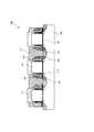
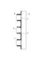
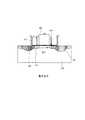
図1は、従来の不揮発性半導体メモリデバイス100の構造を示す断面図である。図1に示す従来の不揮発性メモリ100は、窒化膜を電荷保持膜とするものである。不揮発性半導体メモリデバイス100は、半導体基板108の上にゲート酸化膜107を介してゲート電極105が形成されている。また、半導体基板108の表面付近には、LDD領域114及び拡散層101が形成されている。ゲート電極(コントロールゲート)105の側面にはマスク酸化膜106、窒化膜110が形成されている。窒化膜110の外側にはサイドウォール109が形成されている。半導体基板108上のゲート電極105の近傍にはコンタクトプラグ(拡散層電極)112が形成されている。 FIG. 1 is a cross-sectional view showing the structure of a conventional nonvolatile
上記のような構造の不揮発性半導体メモリデバイス100の製造に際しては、まず、公知の技術によりコントロールゲート105を形成した後、マスク酸化膜106、窒化膜110を半導体基板108上、及びコントロールゲート105の側壁に形成する。次に、コントロールゲート105の側面に窒化膜109を公知の技術によりサイドウォール状に形成する。コントロールゲート105とサイドウォール膜109との間に、マスク酸化膜106と窒化膜110が存在する構造となる。なお、コンタクトプラグ112は公知の技術であるSAC(Self Aligned Contact)構造を用いて、隣接するゲート電極105から100nm以下の近い距離に形成される。窒化膜110の中で電荷が蓄積される領域は、コントロールゲート105の両側の部分であり、1つのコントロールゲート105によってこれら2ビットの書き込みを制御する。 In manufacturing the nonvolatile
不揮発性半導体メモリデバイス100の書き込みの動作は、拡散層101に6V、拡散層102に0Vのバイアスを与え、コントロールゲート105に10Vの電圧を印加する。ソースとなる拡散層102から供給される電子は、一部ホットチャネルエレクトロンとなり拡散層103側の電荷蓄積窒化膜110に注入される。逆に、拡散層102側の電荷蓄積窒化膜110に電子を注入する時には、拡散層101と拡散層102のバイアスを逆にすればよい。 In the writing operation of the nonvolatile
電気消去時の動作は、拡散層101、102に6V、コントロールゲート105に−6Vを印加する。拡散層付近で発生したホットホールはコントロールゲート105の電界により、電荷蓄積窒化膜110に注入される。これにより、電荷蓄積窒化膜110にトラップされている電子を電気的にキャンセルし、電気消去を完了する。 In the operation during electrical erasing, 6 V is applied to the
ここで、電荷蓄積膜110への電子の注入は、ホットチャネルエレクトロンにより行われる。これに対して、電荷蓄積膜110へのホール注入は、ホットホール注入であり、注入原理が異なる。微細化によりゲート電極105と拡散層電極112との距離が短くなった場合、特にSAC構造により拡散層電極112を形成した場合には、拡散層電極112側の電界の影響が大きくなり、それぞれの注入方式での電荷蓄積膜に対する注入分布が変わる。 Here, injection of electrons into the
ゲート電極105と拡散層電極112との距離が長い場合(100nm以上)には、拡散層境界で発生した電子はゲート電極105に影響を受け、電荷蓄積膜110のゲート電極105側に近い部分に注入される(図2参照)。同様に、拡散層境界で発生したホールも電荷蓄積膜110中のゲート電極105に近い部分に注入され、効率よく電気消去を行うことができる(図3参照) When the distance between the
これに対して、SAC構造などによりゲート電極105と拡散層電極112との距離が短く(100nm以下)なると、拡散層と基板108の境界付近で発生した電子は拡散層電極112の電界にも強く影響され、電荷蓄積膜110中の横方向に広く分布する(図4参照)。一方、ホールは逆に拡散層の電界に反発し電荷蓄積膜110中の、よりゲート電極105に近い部分に注入される(図5参照)。これにより、電子とホールの注入分布に差が生じ、結果として、完全に電気消去が行われずに電子が残ってしまう場合がある(図6参照)。これは、電気消去特性を著しく劣化させる原因となる。 On the other hand, when the distance between the
なお、特許文献1には本発明に関連する技術が開示されている。
本発明は上記のような状況に鑑みてなされたものであり、電気消去特性の向上に寄与する不揮発性メモリデバイス及びその製造法を提供することを目的とする。 The present invention has been made in view of the above situation, and an object of the present invention is to provide a nonvolatile memory device that contributes to an improvement in electrical erasure characteristics and a method for manufacturing the same.
上記のような課題を解決ために、本発明の第1の態様に係る不揮発性メモリデバイスは、半導体基板と;前記半導体基板上に形成されたゲート電極と;前記半導体基板上に形成され、前記ゲート電極に近接して形成された拡散層電極と;前記ゲート電極の側面に形成され、注入された電子を保持する電荷蓄積層と;前記拡散層電極の下部に形成されたLDD領域とを備える。そして、前記電荷蓄積層は、前記ゲート電極の側面にのみ形成され、前記LDD領域に沿って延在しない構造であることを特徴とする。 In order to solve the above problems, a nonvolatile memory device according to a first aspect of the present invention includes a semiconductor substrate; a gate electrode formed on the semiconductor substrate; A diffusion layer electrode formed in the vicinity of the gate electrode; a charge storage layer formed on a side surface of the gate electrode and holding injected electrons; and an LDD region formed under the diffusion layer electrode. . The charge storage layer is formed only on a side surface of the gate electrode and has a structure that does not extend along the LDD region.
本発明は、例えば、前記拡散層電極がSAC工程によって形成され、前記ゲート電極と前記拡散層電極との間隔が100nm以下である場合に特に有効である。 The present invention is particularly effective when, for example, the diffusion layer electrode is formed by a SAC process, and the distance between the gate electrode and the diffusion layer electrode is 100 nm or less.
本発明の第2の態様に係る不揮発性メモリデバイスの製造方法は、半導体基板上にゲート電極を形成する工程と;前記半導体基板表面にLDD領域を形成する工程と;前記ゲート電極表面に電荷蓄積層を形成する工程と;前記電荷蓄積層をエッチングすることにより、当該電荷蓄積層が前記ゲート電極の側面にのみ形成され、前記LDD領域に沿って延在しないように形成する工程と;前記ゲート電極に近接して拡散層電極を形成する工程とを含むことを特徴とする。 A method of manufacturing a nonvolatile memory device according to a second aspect of the present invention includes: a step of forming a gate electrode on a semiconductor substrate; a step of forming an LDD region on the surface of the semiconductor substrate; and a charge accumulation on the surface of the gate electrode. Forming a layer; etching the charge storage layer so that the charge storage layer is formed only on the side surface of the gate electrode and not extending along the LDD region; and And a step of forming a diffusion layer electrode in the vicinity of the electrode.
ここで、「電荷蓄積層がゲート電極の側面にのみ形成され、LDD領域に沿って延在しない」とは、電荷蓄積層がゲート電極の側面にのみ形成され、その厚さ以上に基板表面(LDD領域)に沿って延びていないと解釈可能である。 Here, “the charge storage layer is formed only on the side surface of the gate electrode and does not extend along the LDD region” means that the charge storage layer is formed only on the side surface of the gate electrode, and the substrate surface ( It can be interpreted as not extending along the (LDD region).
上述したように、従来の構造においては、SAC構造などを用いて電極間の距離100nm以下にまで近づけた場合には、LDD領域上部の電荷蓄積膜に電子が注入されてしまう。これに対して、本発明の構造においては、電荷蓄積膜中の電子が注入される部分を、ゲート電極側面のみに規制することができる。すなわち、LDD領域上部に電荷蓄積膜が存在しない構造としている。このため、電子とホールの注入分布が一致し、効率よく、電気消去を行うことが可能となる。 As described above, in the conventional structure, when the distance between the electrodes is reduced to 100 nm or less using the SAC structure or the like, electrons are injected into the charge storage film above the LDD region. On the other hand, in the structure of the present invention, the portion into which electrons are injected in the charge storage film can be restricted only to the side surface of the gate electrode. In other words, the charge storage film does not exist above the LDD region. For this reason, the electron and hole injection distributions coincide with each other, and electrical erasing can be performed efficiently.
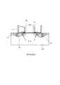
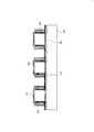
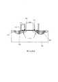
図7は、本発明の実施例に係る不揮発性半導体メモリデバイス200の構造を示す断面図である。図7に示す不揮発性メモリデバイス200は、窒化膜を電荷保持膜とするものである。不揮発性半導体メモリデバイス200は、半導体基板208の上にゲート酸化膜207を介してゲート電極205が形成されている。また、半導体基板208の表面付近には、LDD領域213及び拡散層202が形成されている。ゲート電極(コントロールゲート)205の側面にはマスク酸化膜206、窒化膜210が形成されている。窒化膜210の外側にはサイドウォール209が形成されている。半導体基板208上のゲート電極205の近傍にはコンタクトプラグ(拡散層電極)212が形成されている。 FIG. 7 is a cross-sectional view illustrating the structure of a nonvolatile
電荷蓄積層(窒化膜)210は、ゲート電極205の側面にのみ形成され、LDD領域213に沿って延在しない構造である。すなわち、電荷蓄積層210がゲート電極205の側面にのみ形成され、その厚さ以上に基板表面(LDD領域)に沿って延びていない構造を採用している。 The charge storage layer (nitride film) 210 is formed only on the side surface of the
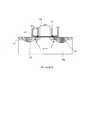
次に、上記のような構造の不揮発性半導体メモリデバイス200の製造工程について、図8〜図16を参照して説明する。まず、半導体基板208の全面に酸化膜を形成する。次に、コントロールゲート205を形成するための膜(ポリシリコンなど)を形成し、パターニングを行うことによりゲート酸化膜207上にコントロールゲート205を成形する。続いて、インプラ工程によりLDD(Light Doped Drain)領域213を形成する(図8参照)。 Next, a manufacturing process of the nonvolatile
次に、図9に示すように、半導体基板208全面にマスク酸化膜206を形成する。続いて、図10に示すように、マスク酸化膜206上に電荷蓄積窒化膜210を形成する。 Next, as shown in FIG. 9, a
その後、図11に示すように、電荷蓄積膜210がゲート電極205の側面にのみ残るようにエッチングを行う。ここでは、半導体基板208に水平な方向へのエッチングレートよりも垂直な方向へのエッチングレートが大きい条件のドライエッチングを行う。
電荷蓄積窒化膜210のエッチング工程においては、ゲート電極205側面には窒化膜210を残す必要があるため、L字型になった窒化膜210の底部のみを除去できるようウェハに垂直方向へのエッチングレートが水平方向に比べて相対的に大きくなるよう設定する。ウェハに平行な方向へのエッチングレートが大きすぎると、L字型になった窒化膜210の底部を除去し終わる前に、ゲート電極205側面の窒化膜210が除去されてしまい、側面の窒化膜210が薄くなりすぎてしまう。逆に、ウェハに垂直方向へのエッチングレートが大きすぎると、L字型になった窒化膜210の底部を除去した後、さらにその下の半導体基板208まで削られてしまうため、微妙な制御を必要とする。例えば、RF100Wにて、CHF3,CF4,O2,Arガスを用いて、10秒程度のエッチングを行う。このようなSAC構造の形成については、特表2002−508589号公報に示されている技術を採用することができる。Thereafter, as shown in FIG. 11, etching is performed so that the
In the etching process of the charge
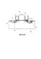
次に、図12に示すように、全面に酸化膜(TOP酸化膜)を形成する。続いて、全面に窒化膜を堆積した後、当該窒化膜がゲート電極205の側面にのみ残るようにエッチングを行い、図13に示すようなサイドウォール209を成形する。ここで行われるエッチングは、半導体基板208に水平な方向へのエッチングレートよりも垂直な方向へのエッチングレートが大きなドライエッチングとする。 Next, as shown in FIG. 12, an oxide film (TOP oxide film) is formed on the entire surface. Subsequently, after a nitride film is deposited on the entire surface, etching is performed so that the nitride film remains only on the side surface of the
次に、図14に示すように、インプラ工程により拡散層201,202を形成する。続いて、コンタクトホール形成のためのストッパー膜215をサイドウォール209の表面に形成した後、層間絶縁膜211を全面に形成する。その後、図15に示すように、層間絶縁膜211の表面にCAP膜216を成形する。 Next, as shown in FIG. 14, diffusion layers 201 and 202 are formed by an implantation process. Subsequently, after a
その後、コンタクトプラグを形成する位置にコンタクトホールを、フォトリソグラフィー工程及びエッチング工程により形成する。次に、図16に示すように、コンタクトプラグ212を埋め込み形成する。なお、コンタクトプラグ212は公知の技術であるSAC(Self Aligned Contact)構造を用いて、隣接するゲート電極205から100nm以下の近い距離に形成される。 Thereafter, contact holes are formed at positions where contact plugs are to be formed by a photolithography process and an etching process. Next, as shown in FIG. 16, a
窒化膜210の中で電荷が蓄積される領域は、コントロールゲート205の両側の部分(203,204)であり、1つのコントロールゲート205によってこれら2ビットの書き込みを制御する。 A region where charges are accumulated in the
図17は、本実施例の不揮発性半導体メモリデバイスの書き込み動作(原理)を示す断面図である。図18は、本実施例の不揮発性半導体メモリデバイスの消去動作(原理)を示す断面図である。図19は、本実施例の不揮発性半導体メモリデバイスの消去後の状態を示す断面図である。 FIG. 17 is a cross-sectional view showing the write operation (principle) of the nonvolatile semiconductor memory device of this example. FIG. 18 is a cross-sectional view showing the erase operation (principle) of the nonvolatile semiconductor memory device of this example. FIG. 19 is a cross-sectional view showing a state after erasure of the nonvolatile semiconductor memory device of this example.
上述した構造の本発明に係るメモリでデバイスによる書き込みの動作においては、図17に示すように、拡散層201に6V、拡散層202に0Vのバイアスを与え、コントロールゲート205に8Vの電圧を印加する。ソースとなる拡散層202から供給される電子は、一部ホットチャネルエレクトロンとなり拡散層203側の電荷蓄積窒化膜210に注入される。逆に、拡散層202側の電荷蓄積窒化膜210に電子を注入する時には、拡散層201と拡散層202のバイアスを逆にすればよい。 In the write operation by the device in the memory according to the present invention having the above-described structure, as shown in FIG. To do. Electrons supplied from the
電気消去時の動作は、図18に示すように、拡散層201、202に6V、コントロールゲート205に−6Vを印加する。拡散層付近で発生したホットホールはコントロールゲート205の電界により、電荷蓄積窒化膜210に注入される。これにより、電荷蓄積窒化膜210にトラップされている電子を電気的にキャンセルし、電気消去を完了する。 As shown in FIG. 18, 6 V is applied to the diffusion layers 201 and 202 and −6 V is applied to the
ここで、電荷蓄積膜210への電子の注入は、ホットチャネルエレクトロンにより行われる。これに対して、電荷蓄積膜210へのホール注入は、ホットホール注入であり、注入原理が異なる。微細化によりゲート電極205と拡散層電極212との距離が短くなった場合、特にSAC構造により拡散層電極212を形成した場合には、拡散層電極212側の電界の影響が大きくなり、それぞれの注入方式での電荷蓄積膜に対する注入分布が変わる。 Here, injection of electrons into the
発明においては、電荷蓄積膜210はゲート電極205側面にのみ存在しているため、図17、図18に示すように、電荷蓄積膜210中の限られた部分にのみ電子が注入される。このため、電子とホールの注入分布が一致するため、図19に示すように、注入された電子を効率よくキャンセルすることが可能となり、電気消去特性が向上する。 In the invention, since the
上述した構造の本発明に係るメモリデバイスによる読み出しの動作においては、1セル2ビットのうち2ビットともブランクの場合は、通常のトランジスタと同様に、セルを挟む二つの拡散層電極212がそれぞれソース、ドレインになり、ゲート電極205に印加される電圧によるチャネルがオンして電流が流れる。一方、1セル2ビットのうち、片側1ビットに電子が注入されている(書き込まれている)状況で、書き込み側を読み出す際には、書き込みビット側の拡散層電極210がソース、未書き込みビット側の拡散層電極210がドレインとなる。この時、注入されている電子による電界の影響で、ソース側のチャネルに空乏層が形成され電流が流れなくなる。逆に未書き込み側を読み出す際は、未書き込みビット側の拡散層電極210がソース、書き込みビット側の拡散層電極210がドレインとなり、注入されている電子による電界の影響が、ドレイン電圧によりキャンセルされ電流が流れる。 In the reading operation by the memory device according to the present invention having the above-described structure, when both of two bits of one cell are blank, the two
以上、本発明の実施例について説明したが、本発明はこれらの実施例に何ら限定されるものではなく、特許請求の範囲に示された技術的思想の範疇において変更可能なものである。 As mentioned above, although the Example of this invention was described, this invention is not limited to these Examples at all, It can change in the category of the technical idea shown by the claim.
200 不揮発性半導体メモリデバイス
205 ゲート電極
208 半導体基板
209 サイドウォール
210 電荷蓄積膜(窒化膜)
212 拡散層電極(コンタクトプラグ)
213 LDD領域
200 Nonvolatile
212 Diffusion layer electrode (contact plug)
213 LDD region
Claims (7)
Translated fromJapanese前記半導体基板上に形成されたゲート電極と;
前記半導体基板上に形成され、前記ゲート電極に近接して形成された拡散層電極と;
前記ゲート電極の側面に形成され、注入された電子を保持する電荷蓄積層と;
前記拡散層電極の下部に形成されたLDD領域とを備え、
前記電荷蓄積層は、前記ゲート電極の側面にのみ形成され、前記LDD領域に沿って延在しない構造であることを特徴とする不揮発性メモリデバイス。A semiconductor substrate;
A gate electrode formed on the semiconductor substrate;
A diffusion layer electrode formed on the semiconductor substrate and formed adjacent to the gate electrode;
A charge storage layer formed on a side surface of the gate electrode and holding injected electrons;
An LDD region formed under the diffusion layer electrode,
The non-volatile memory device, wherein the charge storage layer is formed only on a side surface of the gate electrode and does not extend along the LDD region.
半導体基板上にゲート電極を形成する工程と;
前記半導体基板表面付近にLDD領域を形成する工程と;
前記ゲート電極表面に電荷蓄積層を形成する工程と;
前記電荷蓄積層をエッチングすることにより、当該電荷蓄積層が前記ゲート電極の側面にのみ形成され、前記LDD領域に沿って延在しないように成形する工程と;
前記ゲート電極に近接して拡散層電極を形成する工程とを含むことを特徴とする不揮発性メモリデバイスの製造方法。The method of manufacturing a nonvolatile memory device according to claim 1,
Forming a gate electrode on a semiconductor substrate;
Forming an LDD region near the surface of the semiconductor substrate;
Forming a charge storage layer on the surface of the gate electrode;
Etching the charge storage layer so that the charge storage layer is formed only on the side surface of the gate electrode and does not extend along the LDD region;
Forming a diffusion layer electrode adjacent to the gate electrode. A method for manufacturing a nonvolatile memory device, comprising:
The method of manufacturing a nonvolatile memory device according to claim 5, wherein the diffusion layer electrode is formed by a SAC process.
Priority Applications (2)
| Application Number | Priority Date | Filing Date | Title |
|---|---|---|---|
| JP2008033383AJP2009194156A (en) | 2008-02-14 | 2008-02-14 | Nonvolatile memory device and manufacturing method thereof |
| US12/206,155US20090206389A1 (en) | 2008-02-14 | 2008-09-08 | Nonvolatile memory device and method of manufacturing the same |
Applications Claiming Priority (1)
| Application Number | Priority Date | Filing Date | Title |
|---|---|---|---|
| JP2008033383AJP2009194156A (en) | 2008-02-14 | 2008-02-14 | Nonvolatile memory device and manufacturing method thereof |
Publications (1)
| Publication Number | Publication Date |
|---|---|
| JP2009194156Atrue JP2009194156A (en) | 2009-08-27 |
Family
ID=40954293
Family Applications (1)
| Application Number | Title | Priority Date | Filing Date |
|---|---|---|---|
| JP2008033383APendingJP2009194156A (en) | 2008-02-14 | 2008-02-14 | Nonvolatile memory device and manufacturing method thereof |
Country Status (2)
| Country | Link |
|---|---|
| US (1) | US20090206389A1 (en) |
| JP (1) | JP2009194156A (en) |
Families Citing this family (1)
| Publication number | Priority date | Publication date | Assignee | Title |
|---|---|---|---|---|
| CN106409838A (en)* | 2016-10-31 | 2017-02-15 | 上海华虹宏力半导体制造有限公司 | Process method of SONOS memory |
Citations (2)
| Publication number | Priority date | Publication date | Assignee | Title |
|---|---|---|---|---|
| JP2005150765A (en)* | 2001-11-21 | 2005-06-09 | Sharp Corp | Semiconductor memory device, manufacturing method and operating method thereof, and portable electronic device |
| JP2008153374A (en)* | 2006-12-15 | 2008-07-03 | Oki Electric Ind Co Ltd | Nonvolatile semiconductor memory |
Family Cites Families (10)
| Publication number | Priority date | Publication date | Assignee | Title |
|---|---|---|---|---|
| US6255172B1 (en)* | 2000-05-10 | 2001-07-03 | United Microelectronics Corp. | Electrically erasable non-volatile memory |
| JP2005064295A (en)* | 2003-08-14 | 2005-03-10 | Oki Electric Ind Co Ltd | Semiconductor nonvolatile memory, method of recording information in the semiconductor nonvolatile memory, and method of reading information from the semiconductor nonvolatile memory |
| US7067362B2 (en)* | 2003-10-17 | 2006-06-27 | Chartered Semiconductor Manufacturing Ltd. | Integrated circuit with protected implantation profiles and method for the formation thereof |
| JP2006302985A (en)* | 2005-04-18 | 2006-11-02 | Renesas Technology Corp | Method for manufacturing nonvolatile semiconductor device |
| TWI284979B (en)* | 2005-05-19 | 2007-08-01 | Powerchip Semiconductor Corp | P-channel memory and operating method thereof |
| JP4906329B2 (en)* | 2005-12-02 | 2012-03-28 | ラピスセミコンダクタ株式会社 | Nonvolatile semiconductor memory device and manufacturing method thereof |
| JP2007157919A (en)* | 2005-12-02 | 2007-06-21 | Oki Electric Ind Co Ltd | Semiconductor device and manufacturing method thereof |
| WO2007070808A2 (en)* | 2005-12-12 | 2007-06-21 | The Regents Of The University Of California | Multi-bit-per-cell nvm structures and architecture |
| TWI270214B (en)* | 2005-12-30 | 2007-01-01 | Ind Tech Res Inst | Non-volatile memory device and fabricating method thereof |
| US8742486B2 (en)* | 2006-02-04 | 2014-06-03 | Spansion, Llc | Flash memory cells having trenched storage elements |
- 2008
- 2008-02-14JPJP2008033383Apatent/JP2009194156A/enactivePending
- 2008-09-08USUS12/206,155patent/US20090206389A1/ennot_activeAbandoned
Patent Citations (2)
| Publication number | Priority date | Publication date | Assignee | Title |
|---|---|---|---|---|
| JP2005150765A (en)* | 2001-11-21 | 2005-06-09 | Sharp Corp | Semiconductor memory device, manufacturing method and operating method thereof, and portable electronic device |
| JP2008153374A (en)* | 2006-12-15 | 2008-07-03 | Oki Electric Ind Co Ltd | Nonvolatile semiconductor memory |
Also Published As
| Publication number | Publication date |
|---|---|
| US20090206389A1 (en) | 2009-08-20 |
Similar Documents
| Publication | Publication Date | Title |
|---|---|---|
| CN101373775A (en) | Semiconductor memory device and manufacturing method thereof | |
| US20060146632A1 (en) | Flash memory device and method for fabricating the same, and programming and erasing method thereof | |
| JP2009094170A (en) | Nonvolatile semiconductor memory and manufacturing method thereof | |
| JP5486884B2 (en) | Nonvolatile semiconductor memory device and manufacturing method thereof | |
| US10192879B2 (en) | Semiconductor device and manufacturing method thereof | |
| JP3630491B2 (en) | Semiconductor device | |
| KR100953050B1 (en) | Nonvolatile Memory Device and Manufacturing Method Thereof | |
| JP5039368B2 (en) | Semiconductor memory device, manufacturing method thereof and driving method thereof | |
| JP2007184466A (en) | Semiconductor device and manufacturing method thereof | |
| KR100885777B1 (en) | Manufacturing method of nonvolatile memory device | |
| JP2009152504A (en) | Nonvolatile memory device and manufacturing method thereof | |
| US20100255672A1 (en) | Method of manufacturing semiconductor device | |
| JPWO2008069325A1 (en) | Semiconductor memory device and semiconductor device | |
| KR100875056B1 (en) | Manufacturing Method of Flash Memory Device | |
| JP2009194156A (en) | Nonvolatile memory device and manufacturing method thereof | |
| TW201826501A (en) | Semiconductor device and method of manufacturing same | |
| JP2007158093A (en) | Nonvolatile semiconductor memory device and manufacturing method thereof | |
| JP2008004831A (en) | Nonvolatile memory transistor, and driving method therefor | |
| JP4016679B2 (en) | Semiconductor device and manufacturing method of semiconductor device | |
| KR100685880B1 (en) | Flash Y pyrom cell and manufacturing method thereof | |
| JP2008205187A (en) | Nonvolatile semiconductor memory device and method of manufacturing nonvolatile semiconductor memory device | |
| JP2007043088A (en) | Semiconductor memory device and manufacturing method of semiconductor memory device | |
| JP2009135214A (en) | Semiconductor memory device and manufacturing method thereof | |
| JP2008010463A (en) | Process for fabricating semiconductor device | |
| JP2007335747A (en) | Semiconductor device and its manufacturing method |
Legal Events
| Date | Code | Title | Description |
|---|---|---|---|
| RD02 | Notification of acceptance of power of attorney | Free format text:JAPANESE INTERMEDIATE CODE: A7422 Effective date:20091202 | |
| A977 | Report on retrieval | Free format text:JAPANESE INTERMEDIATE CODE: A971007 Effective date:20091208 | |
| A131 | Notification of reasons for refusal | Free format text:JAPANESE INTERMEDIATE CODE: A131 Effective date:20091222 | |
| A521 | Request for written amendment filed | Free format text:JAPANESE INTERMEDIATE CODE: A523 Effective date:20100212 | |
| A02 | Decision of refusal | Free format text:JAPANESE INTERMEDIATE CODE: A02 Effective date:20100316 |