JP2009187342A - Touch panel, electro-optical device and electronic apparatus - Google Patents
Touch panel, electro-optical device and electronic apparatusDownload PDFInfo
- Publication number
- JP2009187342A JP2009187342AJP2008027316AJP2008027316AJP2009187342AJP 2009187342 AJP2009187342 AJP 2009187342AJP 2008027316 AJP2008027316 AJP 2008027316AJP 2008027316 AJP2008027316 AJP 2008027316AJP 2009187342 AJP2009187342 AJP 2009187342A
- Authority
- JP
- Japan
- Prior art keywords
- light
- electro
- light source
- touch panel
- substrate
- Prior art date
- Legal status (The legal status is an assumption and is not a legal conclusion. Google has not performed a legal analysis and makes no representation as to the accuracy of the status listed.)
- Pending
Links
- 238000001514detection methodMethods0.000claimsabstractdescription166
- 239000004973liquid crystal related substanceSubstances0.000claimsdescription82
- 239000000758substrateSubstances0.000claimsdescription53
- 230000008859changeEffects0.000claimsdescription16
- 230000003287optical effectEffects0.000claimsdescription16
- 239000011159matrix materialSubstances0.000claimsdescription10
- 238000011109contaminationMethods0.000claimsdescription7
- 230000003373anti-fouling effectEffects0.000claimsdescription3
- 239000000382optic materialSubstances0.000claims3
- 230000000694effectsEffects0.000description34
- 239000010408filmSubstances0.000description24
- 239000010410layerSubstances0.000description20
- 239000000463materialSubstances0.000description14
- 238000005286illuminationMethods0.000description13
- 230000004048modificationEffects0.000description10
- 238000012986modificationMethods0.000description10
- 238000010586diagramMethods0.000description6
- 239000011521glassSubstances0.000description6
- 238000009434installationMethods0.000description6
- 239000002346layers by functionSubstances0.000description6
- 230000015572biosynthetic processEffects0.000description5
- 238000000034methodMethods0.000description5
- 239000011347resinSubstances0.000description5
- 229920005989resinPolymers0.000description5
- 238000004519manufacturing processMethods0.000description4
- 230000008569processEffects0.000description3
- 230000009467reductionEffects0.000description3
- 230000007704transitionEffects0.000description3
- 229910052782aluminiumInorganic materials0.000description2
- XAGFODPZIPBFFR-UHFFFAOYSA-NaluminiumChemical compound[Al]XAGFODPZIPBFFR-UHFFFAOYSA-N0.000description2
- 230000002238attenuated effectEffects0.000description2
- 230000008901benefitEffects0.000description2
- 230000005540biological transmissionEffects0.000description2
- 230000004397blinkingEffects0.000description2
- 230000001413cellular effectEffects0.000description2
- 239000004020conductorSubstances0.000description2
- AMGQUBHHOARCQH-UHFFFAOYSA-Nindium;oxotinChemical compound[In].[Sn]=OAMGQUBHHOARCQH-UHFFFAOYSA-N0.000description2
- 230000010287polarizationEffects0.000description2
- 230000001681protective effectEffects0.000description2
- 239000010409thin filmSubstances0.000description2
- 238000002834transmittanceMethods0.000description2
- 239000004925Acrylic resinSubstances0.000description1
- 229920000178Acrylic resinPolymers0.000description1
- FYYHWMGAXLPEAU-UHFFFAOYSA-NMagnesiumChemical compound[Mg]FYYHWMGAXLPEAU-UHFFFAOYSA-N0.000description1
- 239000004642PolyimideSubstances0.000description1
- 230000015556catabolic processEffects0.000description1
- 230000003749cleanlinessEffects0.000description1
- 230000001276controlling effectEffects0.000description1
- 238000006731degradation reactionMethods0.000description1
- 238000009826distributionMethods0.000description1
- 238000005516engineering processMethods0.000description1
- 239000011229interlayerSubstances0.000description1
- 229910052749magnesiumInorganic materials0.000description1
- 239000011777magnesiumSubstances0.000description1
- 238000003909pattern recognitionMethods0.000description1
- 239000004033plasticSubstances0.000description1
- 229920005668polycarbonate resinPolymers0.000description1
- 239000004431polycarbonate resinSubstances0.000description1
- 229920001721polyimidePolymers0.000description1
- 239000010453quartzSubstances0.000description1
- 230000001105regulatory effectEffects0.000description1
- 239000004065semiconductorSubstances0.000description1
- 238000004904shorteningMethods0.000description1
- VYPSYNLAJGMNEJ-UHFFFAOYSA-Nsilicon dioxideInorganic materialsO=[Si]=OVYPSYNLAJGMNEJ-UHFFFAOYSA-N0.000description1
- 230000002123temporal effectEffects0.000description1
Images


Landscapes
- Position Input By Displaying (AREA)
Abstract
Translated fromJapaneseDescription
Translated fromJapanese本発明は、タッチパネル、液晶表示装置等の電気光学装置及び電子機器に関する。 The present invention relates to an electro-optical device and an electronic apparatus such as a touch panel and a liquid crystal display device.
従来、2つの表示範囲のそれぞれに異なる画像を表示することで、視認者に立体画像を認識させることの可能な液晶表示装置等の電気光学装置(以下、「立体画像表示装置」ということがある。)が提案されている。これは、前記2つの表示範囲それぞれを、視認者の右眼及び左眼に対応させるとともに、両表示範囲に若干異なる内容の右眼用画像及び左眼用画像を表示することで視差を生じさせ、これにより当該視認者に立体感を感じさせることが可能な画像表示装置である。
一方、従来、いわゆるタッチパネルが提供されている。これは、画像表示面におけるユーザの指等の接触位置を検出することを通じて、そのユーザの意思・指令等を当該装置に伝えることの可能な装置である。このタッチパネルは、直感的な操作を許容することから、きわめてユーザフレンドリーな側面をもち、券売機、銀行ATM、カー・ナビゲーションシステム等々の構成要素として広く普及している。Conventionally, an electro-optical device such as a liquid crystal display device (hereinafter referred to as a “stereoscopic image display device”) that allows a viewer to recognize a stereoscopic image by displaying different images in two display ranges. .) Has been proposed. This causes the two display ranges to correspond to the right eye and left eye of the viewer, and causes parallax by displaying right eye images and left eye images having slightly different contents in both display ranges. Thus, the image display device can make the viewer feel a stereoscopic effect.
On the other hand, so-called touch panels are conventionally provided. This is a device capable of transmitting the user's intention / command to the device by detecting the contact position of the user's finger or the like on the image display surface. Since this touch panel allows intuitive operation, it has a very user-friendly aspect and is widely used as a component of ticket vending machines, bank ATMs, car navigation systems, and the like.
以上述べた立体画像表示装置及びタッチパネルは一個の装置として共存し得る。そのような装置としては、例えば特許文献1に開示されているようなものが知られている。
ところで、上述したタッチパネルには、その位置検出機能が正確に発揮されるような構造、あるいは原理等の開発が期待されるのは勿論、一般的に、次のような課題もある。
すなわち、タッチパネルは、通常、画像表示機能を担う装置と一体的な関係をもつが、その性質上、その画像表示面を覆うように接触位置検出面(以下、この〔…解決…課題〕の項では、単に「接触面」という。)が設置されることが多い。しかし、そのため、画像を構成する光は、当該接触面を透過してくる必要があり、一定程度その減衰が生じることは避け得ない。あるいは、当該接触面で外光が反射することにより、表示画像のコントラストを低下させるという問題もある。要するに、タッチパネルの設置は、表示画像の品質に影響を与えるおそれが大きいのである。By the way, in general, the touch panel described above is expected to develop a structure, a principle, or the like that can accurately exhibit its position detection function, and generally has the following problems.
In other words, the touch panel usually has an integral relationship with a device responsible for the image display function, but due to its nature, the touch position detection surface (hereinafter referred to as “[Solution… Problem]”) covers the image display surface. Then, it is simply called “contact surface”). However, for this reason, the light constituting the image must be transmitted through the contact surface, and it is inevitable that the light is attenuated to a certain extent. Alternatively, there is a problem in that the contrast of the display image is lowered by reflecting external light on the contact surface. In short, the installation of the touch panel is likely to affect the quality of the display image.
このことは、前述した立体画像表示装置と、タッチパネルとが一個の装置を構成する場合、特に懸念される。立体画像表示装置は、上述のように、微妙な視差を生じさせることで視認者に立体感を感じさせる装置であるから、この視差を具体的にどのように設定するかが極めて重要である。しかるに、前記接触面は、この設定された視差に影響を与え、立体画像を歪ませる等のおそれが高いのである。 This is particularly a concern when the above-described stereoscopic image display device and the touch panel constitute one device. As described above, the stereoscopic image display device is a device that causes a viewer to feel a stereoscopic effect by generating a subtle parallax. Therefore, how the parallax is specifically set is extremely important. However, the contact surface has a high risk of affecting the set parallax and distorting the stereoscopic image.
前述の特許文献1において、「タッチパネルセンサー170」は、「透明な樹脂層内に」、「透明な導電性樹脂からなる複数本の横線とこれに対応する…複数本の縦線」から構成され、指等の接触位置に応じた、「横線と縦線との静電容量の変化」を検知することで、位置検出機能を発揮する(以上、「」内は特許文献1の〔0030〕)。しかし、このような構成はまさに、前述した不具合の発生を懸念させる。「透明」とはいえ、線状の導電性樹脂が格子状に配列された構成では、前記でいうところの接触面において、反射、回折、散乱等々の比較的複雑な光の挙動を生じさせるおそれが高いからである。 In the above-mentioned Patent Document 1, the “touch panel sensor 170” is composed of “inside a transparent resin layer”, “a plurality of horizontal lines made of a transparent conductive resin and a corresponding plurality of vertical lines”. The position detection function is exhibited by detecting “change in capacitance between horizontal line and vertical line” according to the contact position of a finger or the like (in the above, “” in Patent Document 1 [0030]). . However, such a configuration is very concerned about the occurrence of the above-mentioned problems. Although it is “transparent”, in a configuration in which linear conductive resins are arranged in a grid, there is a risk of causing relatively complicated light behavior such as reflection, diffraction, scattering, etc. on the contact surface as described above. Because it is expensive.
本発明は、上述した事情に鑑みてなされたものであり、前述した課題の全部又は一部を解決することの可能な、タッチパネル、液晶表示装置等の電気光学装置及び電子機器を提供することを課題とする。 The present invention has been made in view of the above-described circumstances, and provides an electro-optical device and an electronic apparatus such as a touch panel and a liquid crystal display device capable of solving all or part of the above-described problems. Let it be an issue.
本発明に係るタッチパネルは、上述した課題を解決するため、点灯及び消灯を繰り返す光源と、その内部に前記光源から導入された光を、少なくともその幅広面で全反射する導光板と、前記幅広面に接触した物体による、前記光に起因する散乱光を検出する光検出手段と、前記光源の点灯時における前記光検出手段の出力と当該光源の消灯時における当該出力との差をとって前記散乱光の有無又は強度を検知することで、前記幅広面上における前記物体の接触位置を検出する位置検出手段と、を備える。 In order to solve the above-described problems, the touch panel according to the present invention is a light source that repeatedly turns on and off, a light guide plate that totally reflects light introduced from the light source therein at least at the wide surface thereof, and the wide surface. The light detection means for detecting the scattered light caused by the light by the object in contact with the light source, and the scattering by taking the difference between the output of the light detection means when the light source is turned on and the output when the light source is turned off Position detecting means for detecting the contact position of the object on the wide surface by detecting the presence or absence or intensity of light.
本発明によれば、まず、前記接触位置の検出が正確に行われ得る(以下、この〔課題…解決…手段〕の項において、〔効果1〕という。)。というのも、本発明においては、位置検出手段が、光検出手段の出力のいわば差分を導出することによって、ユーザの指等の物体による前記散乱光を検知するようになっているからである。ここで“差分”は、光源の点灯時と消灯時との間に関してとられる。したがって、例えば、前記幅広面に、タッチパネルの外部から入射する光の影響は、この差分によってキャンセルされ得る一方、前記散乱光の検知がより確実に行われる。また、当該タッチパネルには、後述するような「画像表示装置」が付設され得るが、この場合、当該画像表示装置に由来する画像表示用の光もまた当該タッチパネルに届く。しかし、このような画像表示用の光の影響も、上述と同様、前記差分によってキャンセルされ得る。
このようにして、本発明においては、物体による散乱光を検出することによって、前記接触位置を検出する原理を採用するにもかかわらず、前述した外部光、あるいは画像表示用の光の影響を受けることなく、正確な位置検出が行われ得るようになっているのである。According to the present invention, first, the detection of the contact position can be performed accurately (hereinafter referred to as [Effect 1] in the section of [Problem: Solution ... Means]). This is because, in the present invention, the position detection means detects the scattered light from an object such as a user's finger by deriving a so-called difference in the output of the light detection means. Here, the “difference” is taken between when the light source is turned on and when the light source is turned off. Therefore, for example, the influence of light incident on the wide surface from the outside of the touch panel can be canceled by this difference, while the detection of the scattered light is performed more reliably. The touch panel may be provided with an “image display device” as described later. In this case, image display light derived from the image display device also reaches the touch panel. However, the influence of such image display light can also be canceled by the difference as described above.
In this way, the present invention is influenced by the above-described external light or image display light even though the principle of detecting the contact position is adopted by detecting scattered light from an object. Therefore, accurate position detection can be performed.
また、本発明のタッチパネルは、前記幅広面にほぼ一致する面に表示され得る画像の品質に影響を与えるおそれが極めて少ない(以下、この〔課題…解決…手段〕の項において、〔効果2〕という。)。なぜなら、前述のように、本発明に係るタッチパネルは、導光板の幅広面に接触した物体の散乱光を検出するという原理に基づいているから、当該導光板は、例えば前記〔…解決…課題〕の項で述べたような「複数本の横線」及び「複数本の縦線」といった、比較的複雑な構造をとる必要がないからである。具体的には例えば、当該導光板は、単なる一枚板のガラス板として準備され得る。したがって、前述したような画像表示用の光は、タッチパネル、ないしは導光板を殆ど減衰すること等なく透過可能なのである。 Further, the touch panel of the present invention has a very low possibility of affecting the quality of an image that can be displayed on a surface that substantially matches the wide surface (hereinafter referred to as [Effect 2] That said.) Because, as described above, the touch panel according to the present invention is based on the principle of detecting scattered light of an object that contacts the wide surface of the light guide plate. This is because it is not necessary to have a relatively complicated structure such as “a plurality of horizontal lines” and “a plurality of vertical lines” as described in the above section. Specifically, for example, the light guide plate can be prepared as a simple glass plate. Therefore, the light for image display as described above can be transmitted through the touch panel or the light guide plate with almost no attenuation.
この発明のタッチパネルでは、前記光源は、有機EL素子を含む、ように構成してもよい。
この態様によれば、前述した本発明に係る効果がより実効的に奏される。その中でも特に、本態様は、前記〔効果2〕、即ち表示画像の品質維持ないし向上に大きく貢献する。というのも、本態様では、光源が有機EL(electro luminescent)素子を含むので、例えば光源として蛍光管を利用する場合に比べて、導光板をより薄くすることが可能(したがって、前記の画像表示用の光の減衰度を更に低めることが可能)となるからである。蛍光管を利用する場合、その外径の微小化には物理的な限界があるが、有機EL素子に関しては、そのような意味における限界は存在しない。In the touch panel of this invention, you may comprise the said light source so that an organic EL element may be included.
According to this aspect, the effects according to the present invention described above are more effectively achieved. In particular, this aspect greatly contributes to [Effect 2], that is, to maintaining or improving the quality of the displayed image. This is because, in this embodiment, since the light source includes an organic EL (electro luminescent) element, it is possible to make the light guide plate thinner as compared with, for example, a case where a fluorescent tube is used as the light source. This is because it is possible to further reduce the attenuation of light. In the case of using a fluorescent tube, there is a physical limit to miniaturization of the outer diameter, but there is no limit in that sense regarding the organic EL element.
また、本発明のタッチパネルでは、前記幅広面を覆うように設けられる反射防止膜を更に備える、ように構成してもよい。
この態様によれば、前述した本発明に係る効果がより実効的に奏される。まず、反射防止膜は導光板における外部光の反射を抑制するので、例えば、表示画像のコントラストを低下させるなどといった不具合は発生せず、前記〔効果2〕は更に実効的になる。また、タッチパネル内における外部光それ自体の、いわばその絶対量の減少が可能にもなるから、前記〔効果1〕も更に実効的になる。Moreover, the touch panel of the present invention may be configured to further include an antireflection film provided so as to cover the wide surface.
According to this aspect, the effects according to the present invention described above are more effectively achieved. First, since the antireflection film suppresses reflection of external light on the light guide plate, for example, the problem of reducing the contrast of the display image does not occur, and [Effect 2] becomes more effective. In addition, since the absolute amount of the external light itself in the touch panel can be reduced, the [Effect 1] is further effective.
また、本発明のタッチパネルでは、前記物体がもつ汚れが前記幅広面に転写するのを防止する汚損防止膜を更に備える、ように構成してもよい。
この態様によれば、前述した本発明に係る効果がより実効的に奏される。まず、前記汚れは、光源出射の光等に起因する散乱光(後述する「撹乱散乱光」に相当する。)の発生原因となりえ、したがって、本来検知すべき散乱光との関係では、呼ばれざるべき“ノイズ”の発生原因となってしまうということになり得る。しかしながら、本態様では、その汚れの幅広面への転写が防止されるのであるから、このような不具合発生のおそれは相当程度軽減され、その結果、前記〔効果1〕がより実効的に奏される。
また、汚れが導光板に不存在であるなら、前記画像表示用の光が当該汚れによってその進行を遮られるということがないから、前記〔効果2〕もより実効的に奏される。Further, the touch panel of the present invention may be configured to further include an antifouling film that prevents the dirt of the object from being transferred to the wide surface.
According to this aspect, the effects according to the present invention described above are more effectively achieved. First, the dirt can be a cause of generation of scattered light (corresponding to “disturbed scattered light” to be described later) caused by light emitted from the light source, and is therefore called in relation to the scattered light that should be detected originally. It can be the cause of “noise” that should be avoided. However, in this aspect, since the transfer of the dirt to the wide surface is prevented, the risk of such a problem is considerably reduced, and as a result, [Effect 1] is more effectively achieved. The
In addition, if the dirt is not present in the light guide plate, the image display light is not blocked by the dirt, and thus [Effect 2] is also more effectively achieved.
また、本発明のタッチパネルでは、前記幅広面に付着した汚れを検知する汚損検知手段を更に備え、前記位置検出手段は、前記散乱光の有無又は強度を検知する際に、前記汚損検知手段による検知結果に応じて、前記汚れに起因する撹乱散乱光の存在を無視する、ように構成してもよい。
この態様によれば、前記汚れに起因する撹乱散乱光の存在が「無視」された上で、本来検知すべき前記物体由来の散乱光の有無又は強度が検知される。よって、前記〔効果1〕がより実効的に奏される。
なお、本態様において、「無視」するということを実現するための具体的態様は、様々であり得る。典型的には例えば、第1に、前記汚損検知手段によって、汚れが前記幅広面のどこに位置するかを特定し、第2に、前記光検出手段によって、位置検出機能の運用前に予め、当該位置における撹乱散乱光の強度を検知しておき、第3に、位置検出機能を運用する際には、光検出手段における、いわば裸の検出結果から、前記第1及び第2の工程によって知られた位置及び強度に基づく影響分を差し引く、等というようである。あるいは、これとは別に、予め知られた前記位置及び強度に基づく影響の分だけ、当該位置以外の光検出手段の出力をかさ上げして考える、等といった態様も、「無視」するということを実現する一態様である。The touch panel according to the present invention further includes a stain detection means for detecting dirt attached to the wide surface, and the position detection means detects the presence or intensity of the scattered light when detecting by the stain detection means. Depending on the result, the presence of disturbed scattered light due to the dirt may be ignored.
According to this aspect, the presence / absence or intensity of the scattered light derived from the object to be detected is detected after the presence of the disturbed scattered light due to the dirt is “ignored”. Therefore, [Effect 1] is more effectively achieved.
In addition, in this aspect, the specific aspect for implement | achieving "ignoring" may be various. Typically, for example, firstly, the stain detection means identifies where the dirt is located on the wide surface, and secondly, the light detection means pre-operates the position detection function before the operation. Detecting the intensity of disturbed scattered light at the position, and thirdly, when operating the position detection function, it is known from the first and second steps from the so-called naked detection result in the light detection means. It seems that the influence based on the position and intensity is subtracted. Or, apart from this, an aspect such as raising the output of the light detection means other than the position by the amount based on the previously known position and intensity is considered to be “ignored”. This is one mode to be realized.
一方、本発明に係る電気光学装置は、上述した課題を解決するため、上述した各種態様のタッチパネルと、前記導光板の幅広面に略一致する面に、電気光学素子の光学的特性の変化に応じた画像を表示する画像表示装置と、を備え、前記画像表示装置は、複数の画素電極が形成される第1基板と、該第1基板に対向配置され、前記画素電極との間で所定の電位差を設定するための対向電極が形成される第2基板と、これら第1基板及び第2基板間に挟持される電気光学物質と、を含み、前記導光板、前記第1基板及び前記第2基板は積層構造をとる。 On the other hand, in order to solve the above-described problems, the electro-optical device according to the present invention can change the optical characteristics of the electro-optical element on the touch panel of the various aspects described above and a surface substantially coinciding with the wide surface of the light guide plate. An image display device that displays a corresponding image, and the image display device is disposed between the first substrate on which a plurality of pixel electrodes are formed and the first substrate. A second substrate on which a counter electrode for setting the potential difference is formed, and an electro-optical material sandwiched between the first substrate and the second substrate, the light guide plate, the first substrate, and the first substrate The two substrates have a laminated structure.
本発明によれば、例えば液晶、あるいは有機EL物質等々の電気光学物質を含む「画像表示装置」を含んで、「電気光学装置」が構成される。かかる「画像表示装置」は、比較的薄く製造することが可能である等の特性を備えるので、これと「タッチパネル」との組み合わせは、あり得る最適な選択肢の1つを提供する。
また、この電気光学装置は、上述した各種態様のタッチパネルを備えてなるので、当然、既に述べた〔効果1〕及び〔効果2〕は同様に奏される。なお、このうち〔効果1〕に関連して、本発明のように、「電気光学装置」が、第1基板、電気光学物質、第2基板、及び導光板という積層構造をもつ場合、前記の画像表示用の光は、これら各層の界面で反射する可能性が高まる。したがって、光検出手段の出力に対する当該光の影響は、前述した一般的記述の場合に比べてより深刻になる可能性がある。しかるに、前述した差分をとることによるキャンセルの原理は、このような場合であっても基本的に同様に妥当する。
要するに、本発明においては、上述したような、より大きな外乱要因の存在が推測される場合であっても、前述のキャンセル原理は妥当するので、前記〔効果1〕は、その意味においてより実効的に享受され得ることになるのである。According to the present invention, an “electro-optical device” is configured to include an “image display device” including an electro-optical material such as a liquid crystal or an organic EL material. Since such an “image display device” has characteristics such as being capable of being manufactured relatively thinly, the combination of this and the “touch panel” provides one of the best possible options.
In addition, since the electro-optical device includes the above-described various types of touch panels, naturally, [Effect 1] and [Effect 2] already described are similarly achieved. Of these, in relation to [Effect 1], as in the present invention, when the “electro-optical device” has a laminated structure of the first substrate, the electro-optical material, the second substrate, and the light guide plate, Image display light is more likely to be reflected at the interface between these layers. Therefore, the influence of the light on the output of the light detection means may be more serious than in the general description described above. However, the principle of cancellation by taking the above-described difference is basically valid in this case as well.
In short, in the present invention, even if the presence of a larger disturbance factor is estimated as described above, the above-mentioned cancellation principle is valid, and thus [Effect 1] is more effective in that sense. It can be enjoyed by.
この発明の電気光学装置では、前記複数の画素電極は、前記第1基板の上でマトリクス状配列に従って並び、前記光検出手段は、複数の光検出素子を含み、前記複数の光検出素子は、前記第1基板の上で、前記マトリクス状配列に応じた所定の配列に従って並ぶ、ように構成してもよい。
この態様によれば、画素電極と光検出素子とが同一の基板(即ち、第1基板)の上に形成されることになるので、「タッチパネル」を含む「電気光学装置」を全体的観点からみた場合の構成・構造が、効率的、簡易、あるいは好適になる。
なお、第1基板が、前記画素電極に加えて、例えば、当該画素電極に画像信号を供給するかどうかを司るスイッチング素子(例えば、薄膜トランジスタ等)を備えるのであれば、このスイッチング素子は、前記光検出素子と同時に、あるいは同一の層を構成する要素として形成されてよい。この場合、いずれの素子も半導体層を含み得るので、そのような場合には、製造容易性が高まり、また製造効率の上昇も見込まれる。In the electro-optical device according to the aspect of the invention, the plurality of pixel electrodes are arranged according to a matrix arrangement on the first substrate, the light detection unit includes a plurality of light detection elements, and the plurality of light detection elements include: The first substrate may be arranged according to a predetermined arrangement corresponding to the matrix arrangement.
According to this aspect, since the pixel electrode and the light detection element are formed on the same substrate (that is, the first substrate), the “electro-optical device” including the “touch panel” is considered from an overall viewpoint. The configuration and structure when viewed are efficient, simple, or suitable.
In addition, in addition to the pixel electrode, for example, if the first substrate includes a switching element (for example, a thin film transistor) that controls whether to supply an image signal to the pixel electrode, the switching element is It may be formed simultaneously with the detection element or as an element constituting the same layer. In this case, since any element can include a semiconductor layer, in such a case, the manufacturability is improved and the manufacturing efficiency is expected to increase.
この態様では、前記位置検出手段は、前記接触位置を検出するにあたり、前記複数の光検出素子それぞれの前記第1基板上における配置位置を参照する、ように構成してもよい。
この態様によれば、前記〔効果1〕が更に実効的に奏される。すなわち、本態様では、光検出素子が、マトリクス状配列に応じた所定の配列に従って並ぶ。簡単には例えば、当該光検出素子も、画素電極と同様、当該マトリクス状配列と同じマトリクス状配列に従って並ぶ、というようである。これによれば、例えば、前述した“差分”により検知される、前記散乱光の有無あるいは強度は、一般に、それら、所定の配列に従って並ぶ光検出素子の1個1個に固有のものとして検知され得ることになる。ところで、前記散乱光は、言うまでもなく「幅広面に接触した物体」によって生じさせられたものである。
このようなことから結局、典型的には例えば、N個ある位置検出素子のうち、散乱光を検出した、ある1個の光検出素子が特定されれば、それと同時に、その光検出素子の位置もまた特定され、その位置を接触位置と認定することで、当該接触位置の検出が可能、ということになる。
このようにして、本態様では前記〔効果1〕が更に実効的に奏される。
なお、本態様を含め、前述した光検出素子を含む態様に関連しては、後述する実施形態中の各種の変形を説明する際における項目番号(2)における説明も参照されたい。In this aspect, the position detection unit may be configured to refer to the arrangement positions on the first substrate of the plurality of light detection elements when detecting the contact position.
According to this aspect, the [Effect 1] is more effectively achieved. That is, in this aspect, the light detection elements are arranged according to a predetermined arrangement corresponding to the matrix arrangement. Briefly, for example, the photodetecting elements are arranged in accordance with the same matrix arrangement as that of the matrix arrangement, like the pixel electrodes. According to this, for example, the presence / absence or intensity of the scattered light detected by the “difference” described above is generally detected as unique to each of the photodetectors arranged in accordance with a predetermined arrangement. Will get. By the way, it goes without saying that the scattered light is generated by the “object in contact with the wide surface”.
As a result, typically, for example, out of N position detection elements, if one light detection element that detects scattered light is identified, at the same time, the position of the light detection element Is identified, and the position can be detected by identifying the position as the contact position.
Thus, in the present embodiment, [Effect 1] is more effectively achieved.
In addition, regarding the aspect including the above-described light detection element, including this aspect, see also the description in item number (2) when describing various modifications in the embodiments described later.
あるいは、前述した光検出素子を含む態様では、前記第2基板上に、前記マトリクス状配列に対応する配列に従って並ぶカラーフィルタを更に備え、前記カラーフィルタは、前記光検出素子に係る前記所定の配列に対応する配列に従って並ぶ光検出素子用フィルタを含む、ように構成してもよい。
この態様によれば、まず、カラーフィルタの存在によってカラー画像表示が可能である。
そして、本態様では特に、このカラーフィルタが光検出素子用フィルタを含む。この光検出素子用フィルタは、光検出素子に係る、前記「所定の配列」に対応する配列に従って並ぶので、好適には、光検出素子の全部が、当該光検出素子用フィルタによっていわば覆われるかのごとき状態が呈されることになる。
このようなことから、本態様によれば、前記〔効果1〕が更に実効的に奏される。というのも、本態様によると、光検出素子と、光検出素子用フィルタとの間に上述のような関係があるので、当該光検出素子には、ある所定の波長域にある光だけが進入するということになり、その結果、光検出素子の出力のうち、前述した外部光(これは一般に白色光である)等による寄与分が、相対的に減少するとみることができるからである。
このように、本態様においては、当該外部光等の、いわば絶対量の減少が可能となるから、前記〔効果1〕は更に実効的に奏されるのである。Alternatively, in the aspect including the above-described light detection elements, the color filter further includes a color filter arranged on the second substrate according to an array corresponding to the matrix-like array, and the color filter includes the predetermined array related to the light detection elements. It may be configured to include a filter for photodetection elements arranged in accordance with the arrangement corresponding to.
According to this aspect, first, a color image can be displayed by the presence of the color filter.
In this embodiment, in particular, the color filter includes a light detection element filter. Since the light detection element filters are arranged according to the arrangement corresponding to the “predetermined arrangement” relating to the light detection elements, preferably, all of the light detection elements are covered by the light detection element filters. A state like this will be presented.
For this reason, according to this aspect, the [Effect 1] is more effectively achieved. This is because, according to this aspect, since there is the above-described relationship between the light detection element and the light detection element filter, only light in a predetermined wavelength region enters the light detection element. As a result, it can be considered that the contribution of the above-described external light (which is generally white light) or the like among the outputs of the light detection element is relatively reduced.
Thus, in this aspect, since the absolute amount of the external light or the like can be reduced, the [Effect 1] is more effectively achieved.
この光検出素子用フィルタを備える態様では更に、前記光源は、前記光検出素子用フィルタの色と同じ色の光を発する、ように構成してもよい。
これによれば、光源から発せられる光は、前記光検出素子用フィルタの色と同じであるから、前記散乱光について、前述したような“絶対量の減少”という事態は生じない。つまり、当該散乱光は、何ら問題なく光検出素子に到達する。
このようなことから、本態様では、光検出素子用フィルタが存在しない場合における位置検出の正確性が維持される。より正確に言えば、光源出射光の色と光検出素子用フィルタの色が同じであることから、位置検出の正確性は、光検出素子用フィルタの存在・不存在に影響を受けないのである。そして、本態様では、そうでありながらも、なお前述した外部光の減少による位置検出の正確性の向上を見込むことができるのである。In the aspect including the light detection element filter, the light source may be configured to emit light having the same color as the color of the light detection element filter.
According to this, since the light emitted from the light source has the same color as that of the filter for the light detection element, the situation of “absolute amount reduction” as described above does not occur with respect to the scattered light. That is, the scattered light reaches the light detection element without any problem.
For this reason, in this aspect, the accuracy of position detection is maintained when there is no photodetection element filter. More precisely, since the color of the light emitted from the light source is the same as the color of the light detection element filter, the accuracy of position detection is not affected by the presence or absence of the light detection element filter. . In this mode, the position detection accuracy can be expected to be improved due to the reduction of the external light as described above.
また、本発明の電気光学装置では、前記電気光学物質から発し又は前記電気光学物質を透過した光を、前記導光板に向けて、相異なる少なくとも2つの方向に沿って進行させるレンズ手段を更に備え、当該電気光学装置は、前記少なくとも2つの方向それぞれに対応する、少なくとも2つの表示範囲の各々に、画像を表示する、ように構成してもよい。
この態様によれば、例えば、立体画像表示、あるいは二画像表示等を行うことができる。前者は、前記表示範囲が2つであり、一方に右眼用画像、他方に左眼用画像を表示するとともに、両者間に適当な視差を設定することで、可能である。このような場合、いま述べたような視差の設定が絡むので、前記〔効果2〕が奏されることは、より切実に待望される。というのも、かかる場合に、表示画像の品質がタッチパネルの存在によって貶められるようなことがあったり、あるいは、せっかく設定した視差に影響が及ぼされるようなことがあったりすると、立体画像が歪む等といったことが生じるからである。
しかるに、本態様では、このような不具合は殆ど発生しない。既に述べたように、前記〔効果2〕は導光板の構造が容易である等の理由によって奏されるのであり、画像の性質が何であるかに関わらないからである。言い換えると、このような立体画像表示を行う場合において、前記〔効果2〕は、より実効的に享受されるということができる。
なお、“二画像表示”については、後の実施形態中における該当する箇所(例えば、図21及びその説明参照。)の説明を参照されたい。The electro-optical device according to the aspect of the invention further includes lens means for causing light emitted from the electro-optical material or transmitted through the electro-optical material to travel in at least two different directions toward the light guide plate. The electro-optical device may be configured to display an image in each of at least two display ranges corresponding to the at least two directions.
According to this aspect, for example, stereoscopic image display or two-image display can be performed. The former is possible by having two display ranges, displaying an image for the right eye on one side and an image for the left eye on the other side, and setting an appropriate parallax between them. In such a case, since the parallax setting as described above is involved, it is more eagerly awaited that the [Effect 2] is achieved. This is because, in such a case, if the quality of the displayed image may be praised due to the presence of the touch panel or the parallax set may be affected, the stereoscopic image may be distorted. This is because of the above.
However, in this embodiment, such a problem hardly occurs. As described above, the above [Effect 2] is achieved because the structure of the light guide plate is easy, and is not related to the nature of the image. In other words, in the case where such a stereoscopic image display is performed, it can be said that [Effect 2] is more effectively enjoyed.
For “two-image display”, refer to the description of the corresponding part in the later embodiment (for example, see FIG. 21 and the description thereof).
この態様では、前記光検出素子は、前記画素電極からみて、前記少なくとも2つの方向の各々に沿って延びる各直線全体が張る平面の法線方向に所定量ずらされた位置に形成される、ように構成してもよい。
これによれば、光検出素子の存在が、例えば前述した視差の設定に影響を及ぼすことが回避される。すなわち、本態様において、光検出素子は、上述したような「ずらされた位置」に形成されていることから、例えば、レンズ手段を透過した光の進行方向を具体的に定めるにあたって、光検出素子の幅や長さ等といったことに関し配慮する必要がない。
以上により、本態様によれば、よりよい立体画像等の表示を行うことができる。
なお、本態様は、上に述べたところから明らかなように、前記「レンズ手段」を備える態様を前提とするとともに、前記「光検出手段」として「光検出素子」を含む態様をも前提とする。In this aspect, the photodetecting element is formed at a position shifted by a predetermined amount in the normal direction of the plane extending from the entire straight line extending along each of the at least two directions when viewed from the pixel electrode. You may comprise.
According to this, it is avoided that the presence of the light detection element affects, for example, the above-described parallax setting. That is, in this aspect, since the light detection element is formed at the “shifted position” as described above, for example, in specifically determining the traveling direction of the light transmitted through the lens unit, the light detection element There is no need to consider the width, length, etc.
As described above, according to this aspect, it is possible to display better stereoscopic images and the like.
As is apparent from the above description, this aspect is premised on an aspect including the “lens means”, and an aspect including a “photodetection element” as the “photodetection means”. To do.
また、前記レンズ手段を備える態様では、前記電気光学物質は液晶を含み、前記画像表示装置は偏光板を更に含み、当該偏光板は、前記レンズ手段に貼り付けられている、ように構成してもよい。
この態様によれば、当該電気光学装置の組立工程等において、偏光板及び導光板は、一体的に、あるいは1個の部品として取り扱われ得ることになるから、製造容易性等が高まる。また、導光板がガラスから作られる場合には、偏光板の存在により当該導光板の破損が未然に防止されるという効果も得られる。In the aspect including the lens unit, the electro-optical material includes a liquid crystal, the image display device further includes a polarizing plate, and the polarizing plate is attached to the lens unit. Also good.
According to this aspect, since the polarizing plate and the light guide plate can be handled integrally or as one component in the assembly process of the electro-optical device, the ease of manufacture and the like is improved. Further, when the light guide plate is made of glass, there is an effect that the light guide plate is prevented from being damaged by the presence of the polarizing plate.
また、本発明の電気光学装置では、前記光源は、前記画像を表示するためのフレーム周波数よりも大きい周波数で、点灯及び消灯を繰り返す、ように構成してもよい。
この態様によれば、前記の画像表示用の光の強度が、例えば時々刻々変動する場合(かかる場合には、典型的には例えば、画像表示装置が動画像を表示する場合等が含まれる。)であっても、そのことが、位置検出機能、あるいは光検出手段ないしその出力に与える影響を一定程度軽減することができる。画像のフレーム切換のタイミングよりも光源点滅のタイミングが速まれば、前記散乱光の検出のタイミングもまた速まり、したがってまた、前述した“差分”は、ある1フレーム期間中の一定の光度環境の中におけるデータとして取得され得ることになるからである。In the electro-optical device according to the aspect of the invention, the light source may be repeatedly turned on and off at a frequency higher than a frame frequency for displaying the image.
According to this aspect, for example, the case where the intensity of the image display light varies from moment to moment (in such a case, typically, for example, a case where the image display device displays a moving image) is included. However, the influence of this on the position detection function or the light detection means or its output can be reduced to some extent. If the timing of the light source blinking is earlier than the timing of switching the frame of the image, the timing of detecting the scattered light is also accelerated. Therefore, the above-mentioned “difference” is also caused by a certain luminous intensity environment during a certain frame period. This is because it can be acquired as data inside.
一方、本発明の電子機器は、上記課題を解決するために、上述した各種態様の電気光学装置を備える。
本発明の電子機器は、上述した各種の電気光学装置を備えてなるので、正確な位置検出機能を享受し得るとともに、高品位な画像を表示することが可能である。On the other hand, in order to solve the above-described problems, an electronic apparatus according to the present invention includes the electro-optical devices of various aspects described above.
Since the electronic apparatus of the present invention includes the various electro-optical devices described above, it can enjoy an accurate position detection function and can display a high-quality image.
<第1実施形態>
以下では、本発明に係る第1の実施の形態について図1乃至図3を参照しながら説明する。なお、これら図1乃至図3並びに以下で参照するその他の各図面においては、各層や各部材を図面上で認識可能な程度の大きさとするため、各層毎や各部材毎に縮尺を異ならせてある場合がある。<First Embodiment>
Hereinafter, a first embodiment of the present invention will be described with reference to FIGS. In FIGS. 1 to 3 and other drawings referred to below, the scales of the respective layers and members are made different for each layer and each member so that each layer and each member can be recognized on the drawings. There may be.
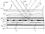
第1実施形態に係る液晶表示装置100は、照明装置LB、液晶装置LD、偏光板30U及び30L、並びに、タッチパネル40から構成されている(これらのうちタッチパネル40を除く各要素(LB,LD,30U,30L)は、本発明にいう「画像表示装置」を構成する。)。この液晶表示装置100の断面をみると、図3に示すように、その全体的な構成の積層順番は、同図中下から、照明装置LB、偏光板30L、第1基板10、液晶層LQ、遮光膜BM及びカラーフィルタCF、第2基板20、偏光板30U、タッチパネル40となっている。 The liquid
照明装置LBは、導光板及び光源からなる(いずれも不図示)。このうち光源は、例えば白色LED(Light Emitting Diode)である。この光源は、例えば、比較的長尺の棒状ないしは直方体形状をもち、その長手方向が、略平板状の導光板の側端に沿うようにして配置される。光源から発せられた光は、導光板の当該側端からその内部に入射する。光源は、照明駆動回路52によって、その点灯・消灯が制御される。 The illumination device LB includes a light guide plate and a light source (both not shown). Among these, the light source is, for example, a white LED (Light Emitting Diode). This light source has, for example, a relatively long rod shape or rectangular parallelepiped shape, and is arranged such that its longitudinal direction is along the side edge of the substantially flat light guide plate. Light emitted from the light source enters the light guide plate from the side end thereof. The light source is controlled to be turned on / off by the illumination drive circuit 52.
液晶装置LDは、図1、あるいは図3に示すように、相互に対向する第1基板10と第2基板20とを備えている。第1基板10と第2基板20との間隙には液晶層LQが位置する(図3参照)。第1基板10及び第2基板20は、例えばガラスや石英、プラスチックなどの透光性材料で作られる。
これら第1基板10及び第2基板20の上には、それぞれ、固有の積層構造物が構築される。As shown in FIG. 1 or FIG. 3, the liquid crystal device LD includes a
A unique laminated structure is constructed on each of the
第1基板10の側では、当該第1基板10の上に、例えば、スイッチング素子としてのTFT(Thin Film Transistor)、走査線、データ線、画素電極、及びこれら各要素間に適宜設けられる透光性の層間絶縁膜等が順次構築される。図1においては、このうち画素電極9及び光検出素子15が図示されている。なお、光検出素子15は、第1実施形態において中心的な機能・役割を担うが、その構成及び作用等についての詳細は後に改めて述べる。
画素電極9は、図1に示すように、平面視してマトリクス状に配列されている(図3では不図示)。この画素電極9は、例えばITO(Indium Tin Oxide)等の透光性かつ導電性材料で作られている。On the
As shown in FIG. 1, the
第1基板10の側には、上述に加えて、前記画素電極9の上に、配向膜(不図示)等が形成される。配向膜は液晶層LQに接する。この配向膜の表面には、液晶層LQを構成する液晶分子の初期配向状態を規制する配向処理が施されている。このような配向膜は、例えばポリイミド等の樹脂材料で作られている。
なお、液晶層LQは、正の誘電率異方性を有する液晶を用いたTNモードで動作する構成をとりうる。
また、上述のような配向膜は、第2基板20の側にも、液晶層LQに直接接する膜として形成されている(当該配向膜も不図示)。On the
Note that the liquid crystal layer LQ can be configured to operate in a TN mode using a liquid crystal having positive dielectric anisotropy.
The alignment film as described above is also formed on the
一方、第2基板20の側では、当該第2基板20の上に(図1及び図3の観点では「下に」ということになる。)、カラーフィルタCF、遮光膜BM、対向電極等が構築される。図1においては、このうちカラーフィルタCFのみが図示されており、図3においては、これに加えて遮光膜BMが図示されている。 On the other hand, on the
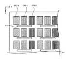
カラーフィルタCFは、図1に示すように、前記の画素電極9の形成領域と呼応するように、平面視してマトリクス状に配列されている(図2における符号“CF1,9”、“CF2,9”及び“CF3,9”のそれぞれは、そのような事情を表現している。)。このカラーフィルタCFは、赤フィルタCF1,緑フィルタCF2及び青フィルタCF3の三種のフィルタを含み、これら各々は、図1あるいは図2に示すように、所定の順番に従って配列される。図2では、X方向(行方向)に沿っては、赤フィルタCF1,緑フィルタCF2及び青フィルタCF3がこの順に配列され、かつ、これを一組とする繰り返し配列がなされるようになっている一方、Y方向(列方向)に沿っては、画素列毎に、赤フィルタCF1の列、緑フィルタCF2の列、及び青フィルタCF3の列が、それぞれ並ぶような配列がなされている。
このカラーフィルタCFは、照明装置LBから発し液晶層LQを透過してきた光のうち、所定の波長域にある光のみを透過させる。つまり、透過光はいわば「着色」される。As shown in FIG. 1, the color filters CF are arranged in a matrix in plan view so as to correspond to the formation region of the pixel electrode 9 (reference numerals “CF1, 9”, “CF2 in FIG. 2”). , 9 "and" CF3, 9 "represent such circumstances). The color filter CF includes three types of filters, a red filter CF1, a green filter CF2, and a blue filter CF3, each of which is arranged in a predetermined order as shown in FIG. 1 or FIG. In FIG. 2, along the X direction (row direction), the red filter CF1, the green filter CF2, and the blue filter CF3 are arranged in this order, and a repeated arrangement is made with this set as a set. On the other hand, along the Y direction (column direction), an array in which a column of the red filter CF1, a column of the green filter CF2, and a column of the blue filter CF3 are arranged for each pixel column.
The color filter CF transmits only light in a predetermined wavelength region out of light emitted from the illumination device LB and transmitted through the liquid crystal layer LQ. In other words, the transmitted light is “colored”.
なお、第1実施形態では、前述の赤フィルタCF1、緑フィルタCF2及び青フィルタCF3の一組によって規定される領域を、特に“1ピクセル”と定義する。この1ピクセルにおいては、前記の3つのフィルタCF1、CF2及びCF3それぞれの光の透過状態に応じて、これらを一組としてみた場合におけるカラードットが表示可能である。言い換えると、この1ピクセルは、液晶装置LDにおいて表示される画像の基礎単位ということができる。 In the first embodiment, an area defined by one set of the red filter CF1, the green filter CF2, and the blue filter CF3 is particularly defined as “1 pixel”. In this one pixel, color dots can be displayed when the three filters CF1, CF2, and CF3 are viewed as a set according to the light transmission state of each of the three filters CF1, CF2, and CF3. In other words, this one pixel can be said to be a basic unit of an image displayed in the liquid crystal device LD.
遮光膜BMは、前述したカラーフィルタCFの形成領域の間を縫うようにして、格子状に形成されている(図1及び図2では明示されていない。図3参照。)。
この遮光膜BMは、隣接する画素間で透過光が交じり合うのを防止する。また、遮光膜BMは、第1基板10上に形成される前記走査線、前記データ線、前記TFT等の不透明な材料を覆う役割も担う。逆に言えば、これら走査線等は、遮光膜BMが格子状をもつことに対応して、格子状領域に配置されるのである。The light shielding film BM is formed in a lattice shape so as to sew between the above-described color filter CF formation regions (not explicitly shown in FIGS. 1 and 2; see FIG. 3).
The light shielding film BM prevents transmitted light from intermingling between adjacent pixels. The light shielding film BM also serves to cover opaque materials such as the scanning lines, the data lines, and the TFTs formed on the
対向電極は、前述したカラーフィルタCF及び遮光膜BMを覆うようにして、第2基板20のほぼ全面に相当する領域に形成されている。対向電極は、前記画素電極9と同様、例えばITO(Indium Tin Oxide)等の透光性かつ導電性材料で作られている。 The counter electrode is formed in a region corresponding to almost the entire surface of the
前述した対向電極と画素電極9は、液晶駆動回路53に接続されている。
この液晶駆動回路53は、前述した走査線に選択信号を供給する走査線駆動回路、及び、前述したデータ線に画像信号を供給するデータ線駆動回路を含む。走査線駆動回路は、1つの画素行を単位として選択信号を発し、水平走査期間を規定する。データ線駆動回路は、走査線駆動回路によって選択された画素行に対して、画像信号を供給する(即ち、画像信号を書き込む。)。最初の画素行に画像信号の供給を開始してから、最終の画素行に画像信号を供給するまでの時間が、垂直走査期間となる。
なお、前記TFTは、前記選択信号の有無に応じて、ON状態及びOFF状態間を遷移し、そのON状態のときに、前記画像信号をデータ線から画素電極9へと伝達する。The counter electrode and the
The liquid crystal driving circuit 53 includes a scanning line driving circuit that supplies a selection signal to the above-described scanning line, and a data line driving circuit that supplies an image signal to the above-described data line. The scanning line driving circuit issues a selection signal in units of one pixel row and defines a horizontal scanning period. The data line driving circuit supplies an image signal to the pixel row selected by the scanning line driving circuit (that is, writes the image signal). The time from the start of the supply of the image signal to the first pixel row to the supply of the image signal to the final pixel row is the vertical scanning period.
The TFT transitions between an ON state and an OFF state according to the presence / absence of the selection signal, and transmits the image signal from the data line to the
以上の結果、各画素について、画素電極9及び対向電極間の電位差が適当に設定されることになり、その間に挟持された液晶層LQ内の液晶分子の配向状態が適当に調整される。これにより、照明装置LBからの出射光のうち観察側に透過する光量の割合(透過率)は画素電極9ごとに制御される。対向電極及び画素電極9間の電位差の大きさ等は、画素電極9に供給される画像信号の状態如何による。これにより、液晶装置LDは、画素電極9が配列された面で、画像を表示する(当該面は、図1から明らかなように、後述する導光板42の幅広面にほぼ相当する。)。
なお、偏光板30Lは、照明装置LBから発せられた光を偏光させ、偏光板30Uは、液晶装置LDを透過してきた光を照明装置LBから発せられた光を偏光させる。これらの偏光板30U及び30Lによる偏光の方向は、液晶層LQを透過する光が受ける偏光の方向に依存して決定される。As a result, for each pixel, the potential difference between the
The
以上の構成に加えて、第1実施形態の液晶表示装置100は特に、タッチパネル40及びこれに関連する構成を備えている。
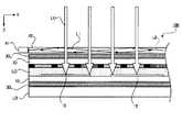
タッチパネル40は、図1あるいは図3に示すように、光源41及び導光板42を備えている。
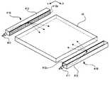
このうち光源41は、複数の発光ダイオード410を含む(図3では不図示)。これら複数の発光ダイオード410は、図1のY方向に沿って一列に配列されており、その発光部分を導光板42の側端面に向けている。図1では、このような構造をもつ光源41が、直方体状の部材として簡略化されて描かれている。なお、第1実施形態では、図1に示すように、かかる光源41が導光板42を挟むようにして2組設けられている。In addition to the above configuration, the liquid
The
Among these, the
一方、導光板42は、略平板状の形態をもつ光透過性の光学部材である。より具体的には、この導光板42は、例えばガラス、あるいはポリカーボネートやアクリル樹脂等の透明樹脂から好適に作られる。また、その厚さ(図1中Z方向に沿った長さ)は、例えば、0.5mmから1mm程度とされて好適である。図から明らかなように、この導光板42は、基本的に、前記光学部材のみからなる、いわば単純な一枚板として準備され得る。
前述のように、前記の2つの光源41は、この導光板42の相互に対向する2つの側端面に沿うように配される。また、これら側端面間に挟まれた2つの幅広面(の内側の面)では、光源41から入射した光が全反射する。これにより、光源41から入射した光は、当該導光板42の側端面からその内部に入射し、該内部全体に行き渡る。あるいは、当該導光板42の内部全体は当該光でいわば満たされるような状態になる。この際、光源41から発した光が、導光板42の内部からその外部に向けて、いわば自発的に出射するという事象は無視しうる程度の影響しか与えない。前記幅広面はそのように調整されている。On the other hand, the
As described above, the two
前記の光源41は、図1に示すように、位置検出回路54に接続されている。
この位置検出回路54は、光源41の点灯及び消灯のタイミングを制御する発光ダイオード駆動回路を含む。また、位置検出回路54は、液晶装置LD中の第1基板10上に形成された、前記光検出素子15に接続されている。The
The
この光検出素子15は、図1、あるいは図2に示すように、概ね長方形状をもち、その長手方向をX方向に一致させ、その短手方向をY方向に一致させている。また、光検出素子15は、図2に示すように、各画素行の間に位置づけられるように配置されている。
このような光検出素子15は、図1、あるいは図2に示すように、3つの画素電極9を一単位として、1個ずつ形成されている。第1実施形態では、ここでいう3つの画素電極9はそれぞれ、赤フィルタCF1、緑フィルタCF2及び青フィルタCF3のそれぞれに対応する(図2参照)。つまり、光検出素子15は、前述した“1ピクセル”を一単位として、1個ずつ形成されているのである。As shown in FIG. 1 or FIG. 2, the
As shown in FIG. 1 or FIG. 2, such
この光検出素子15は、該素子15に入射する光の強度に応じた大きさをもつ電流を発生する機能をもつ。具体的には、フォトダイオードが利用されて好適である。なお、光検出素子15の光検出面は、図1、あるいは図3中上方向を向いている。つまり、光検出素子15は、当該検出面を導光板42の幅広面に対向させるように、配置されているのである。これにより、光検出素子15は、照明装置LBから発した光の入射を直接に受けて、これを電流に変換することはない。 The
位置検出回路54は、以上のような光検出素子15からの出力を受ける。光検出素子15は、既述のように1ピクセルごとに配置されているから、どの光検出素子15からの出力に変化があったか等を観察・検知することにより、位置検出回路54は、その変化のあった光検出素子15の配置場所に対応する“位置”を検出することが可能である。なお、ここでいう位置は、明らかに、図1あるいは図2等のXY平面内における位置である。 The
以下では、以上のような構成を備える液晶表示装置100の動作について、既に参照した図1乃至図3に加えて、図4乃至図9を参照しながら説明する。
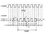
位置検出回路54中の発光ダイオード駆動回路は、光源41を構成する発光ダイオード410の点灯及び消灯のタイミングを、図4の上段に示すように制御する。すなわち、光源41は、期間T1において消灯、期間T2において点灯、が繰り返されるように制御される。この繰り返し周波数は、基本的に任意に設定可能であるが、好適には例えば60Hz程度とする。なお、第1実施形態では、T1=T2であるが、場合によっては、T1≠T2としてもよい。
このような制御により、光源41を出射した光が導光板42の内部に満たされる状態が間欠的に訪れる。Hereinafter, the operation of the liquid
The light emitting diode drive circuit in the
By such control, the state where the light emitted from the
このような状況の下、ユーザが、タッチパネル40の表面、即ち導光板42の幅広面に接触すると、以下のような状態変化が観測される。
まず、第1に、ユーザの指等の接触時点が、前記の期間T1内である場合、光源41出射の光に起因する変化は当然ながら生じない。一方、当該接触時点が、前記の期間T2内である場合、光源41出射の光は、当該指等の表面で散乱する。この散乱光は、光検出素子15に入射して、電流を発生させる。図4の下段において、符号SLが付され、実線で表されたパルスは、このような状況を表現している。Under such circumstances, when the user contacts the surface of the
First, when the contact time of the user's finger or the like is within the period T1, the change due to the light emitted from the
ここで第2に、光検出素子15は、当該液晶表示装置100の外部からその内部に進入しようとする光(以下、「外光」という。)と、照明装置LBから発した光が当該液晶表示装置100の内部の適当な界面で反射した光(以下、「内光」という。)との影響を受けることに注意する。 Here, secondly, the
まず、“外光”に関する影響について、図6及び図7を参照してより詳細に説明する。
なお、図6及び図7は、期間T2、即ち光源41から導光板42に光が入射している状態を表している(符号L1及びL2参照)。ちなみに、符号L1及びL2は、前者(L1)がこれら図6及び図7中左側に位置する光源41からの入射光を、後者(L2)が図示されない右側に位置する光源41からの入射光を、それぞれ表しているが、これらの区別は便宜上のものに過ぎない。いずれにせよ、光源41からの光は、図示するように導光板42の幅広面で全反射することにより、当該導光板42の内部全体を満たすことになる。First, the influence on “external light” will be described in more detail with reference to FIGS. 6 and 7.
6 and 7 show a period T2, that is, a state in which light is incident on the
さて、ユーザの指が導光板42に接触していない状態では、図6に示すように、外光LOは、そのまま液晶表示装置100の内部に進行する。したがって、光検出素子15は、この外光LOの入力を受けて、電流を発生させる。
他方、ユーザの指FUが導光板42に接触すると、図7に示すように、外光LOは、その進行が遮られる。進行が遮られるのは、指FUが存在する位置であって、それ以外の場所では外光LOの挙動に変化はない。ちなみに、指FUにより、光源41からの入射光L1ないしL2が散乱を受けることは既に述べたとおりである(図7では、散乱光SL1として図示されている。)。Now, in a state where the user's finger is not in contact with the
On the other hand, when the user's finger FU comes into contact with the
このような状態遷移により、光検出素子15は、図6の状態では、外光LO由来の、より大きな電流を発生し、図7の状態では、外光LO由来の、より小さな電流を発生する。また、図7の状態では、光検出素子15は、光源41、即ち散乱光SL1由来の電流も発生する。
図4下段において、破線及び実線で示す検出波形は、これをまとめた結果である。つまり、指FUが触れていないときには、光検出素子15は大きさΔ1の電流を発生し、触れているときには大きさΔ2(<Δ1)の電流を発生するとともに、大きさSLの電流を発生する。なお、外光LO由来の電流それ自体は、期間T1及びT2の区別(即ち、光源41の点灯・消灯)とは無関係である。Due to such state transition, the
In the lower part of FIG. 4, the detection waveforms indicated by a broken line and a solid line are a result of putting these together. That is, when the finger FU is not touching, the
次に、“内光”に関する影響について、図8及び図9を参照してより詳細に説明する。なお、図8及び図9は、期間T1、即ち光源41から導光板42に光が入射していない状態を表している。 Next, the influence on “inner light” will be described in more detail with reference to FIGS. 8 and 9. 8 and 9 show a period T1, that is, a state where light is not incident on the
まず、ユーザの指が導光板42に接触していない状態では、図8に示すように、内光LIは、光検出素子15にそのまま入力する。図においては、内光LIの例として、照明装置LBから発した光(符号“LId”参照)が、偏光板30Uの図中上面で反射した光、及び、導光板42の図中上面で反射した光がそれぞれ示されている。内光LIは、その他の界面における反射光をも含み得る。
他方、ユーザの指FUが導光板42に接触すると、図9に示すように、内光LIは、この指FUの表面で散乱する(図9中、散乱光SL2参照。)。この散乱が生じるのは、指FUが存在する位置であって、それ以外の場所では内光LIの挙動に変化はない。First, in a state where the user's finger is not in contact with the
On the other hand, when the user's finger FU contacts the
このような状態遷移により、光検出素子15は、図8の状態では、内光LI由来の、より小さな電流を発生し、図7の状態では、内光LI由来の、より大きな電流を発生する。後者において、より大きな電流が発生するのは、既述のように、光検出素子15が、指FUによる散乱光SL2由来の電流をも発生させるからである。
図4下段において、一点鎖線で示す検出波形は、これをまとめた結果である。つまり、指FUが触れていないときには、光検出素子15は大きさΔ3の電流を発生し、触れているときには大きさΔ4(>Δ3)の電流を発生する。なお、内光LI由来の電流それ自体も、外光LOの場合と同様、期間T1及びT2の区別とは無関係である。Due to such a state transition, the
In the lower part of FIG. 4, the detection waveform indicated by the alternate long and short dash line is a result of summarizing the detection waveforms. That is, when the finger FU is not touching, the
以上のようなことから、図4の全体は結局以下のように解釈される。すなわち、ユーザの指FUが導光板42に触れていない期間においては、光検出素子15は、外光LO由来の大きさΔ1の電流及び内光LI由来の大きさΔ3の電流を合算した電流を発生する。この状態は、外光LO及び内光LIの大きさに変化がない以上は、変化がない。また、光源41の点灯及び消灯の状態変化にも影響を受けない。
他方、指FUが導光板42に触れている期間(即ち、図4中の「接触期間」)においては、光検出素子15は、外光LO由来の大きさΔ2の電流及び内光LI由来の大きさΔ4の電流(指FUによる散乱光SL2由来の電流を含む。)、並びに、指FUによる散乱光SL1由来の大きさSLの電流、のそれぞれを合算した電流を発生する。この状態は、前二者の電流に関しては、上述のΔ1及びΔ3に関する記述と同様のことが言えるが、後一者の電流は、光源41の点灯及び消灯の状態変化に影響を受ける。これが、図4中実線で示されるパルスとなって現われる。なお、光検出素子15は、その受けた光の強度に応じた電流を発生することから、当該パルスの高さは、散乱光SL1の強度を意味しているとみることができる。From the above, the whole of FIG. 4 is finally interpreted as follows. That is, in a period when the user's finger FU is not touching the
On the other hand, during the period in which the finger FU is in contact with the light guide plate 42 (that is, the “contact period” in FIG. 4), the
位置検出回路54は、このような検出結果に基づいて、図5に示すような波形を演算、導出する。ここで図5は、図4中の検出波形において、相隣接する期間T1及びT2間の差分をそれぞれとり、かつ、それらを相互に接続することにより得られる、差分波形である。図4に関する上述したような性格により、指FUが導光板42に接触しないとき差分は0であり、接触するとき大きさSLに対応する差分が得られることになる。
このようにして、指FUの接触が検出される。
後は、このような差分波形の導出の元となった光検出素子15が、図2等に示す各光検出素子15のうちのどれであったかを確認すれば、指FUが、導光板42のどこに触れたかを検出することが可能になる。The
In this way, contact with the finger FU is detected.
After that, if it is confirmed which of the
以上のような構成及び作用をもつ液晶表示装置100によれば、次のような効果が奏される。
(1) まず、第1実施形態の液晶表示装置100、あるいはタッチパネル40によれば、外光LO及び内光LIの影響を受けずに、きわめて正確に指FUの接触位置の検出を行うことができる。これは、上述のように、光源41を点滅させること、及び、図5のような差分波形をとることに基づき指FUの散乱光の変化が求められることによっている。すなわち、図5のような差分をとることにより、外光LO及び内光LIの影響はいわばキャンセルされることから、光源41に起因する指FUによる散乱光の検出が比較的厳密に行われることになり、その結果、位置検出の正確性も高まるのである。According to the liquid
(1) First, according to the liquid
なお、これに関連して、外光LO及び内光LIの強度は、一般に、XY平面内において均一であるとは限らない。外光LOに関して言えば、例えば、太陽光、あるいは室内照明光がXY平面に対して斜めに射し込んでいる等という場合、XY平面内の当該外光LOの強度は、例えばY方向に沿って次第に低下していく等ということがあり得る。また、内光LIに関しては、その大元(図8のLId参照)は液晶層LQを透過してくる画像を表示するための光であるから、XY平面内の当該内光LIの強度は、場所場所に応じて相違するのがむしろ通常状態と考えることもできる。
このようであるから、これら外光LO及び内光LIが光検出素子15に与える、より実際的な影響は、図4、あるいは図6乃至図9を参照して説明したような場合に比べて、より複雑なものになることが考えられる(これは即ち、正確な位置検出を行おうとするにあたって、より深刻な事態といえる。)。
しかるに、第1実施形態によれば、このような複雑さ、あるいは深刻さが相当程度軽減される。というのも、既に述べたように、第1実施形態では、位置検出回路54が、図5のような差分波形をとるからである。これにより、XY平面内で外光LO及び内光LIの強度分布がみられるような場合であっても、ある1個の光検出素子15の検出結果についての直前・直後間の差分をとれば、結局、当該光検出素子15に関する前記複雑さ等はキャンセルされてしまうからである。このことは、図2等に示す光検出素子15の全部に関してもあてはまる。In this regard, in general, the intensity of the external light LO and the internal light LI is not always uniform in the XY plane. With regard to the external light LO, for example, when sunlight or indoor illumination light is obliquely incident on the XY plane, the intensity of the external light LO in the XY plane is, for example, along the Y direction. It is possible that it will gradually decrease. Further, with respect to the internal light LI, the principal element (see Lid in FIG. 8) is light for displaying an image transmitted through the liquid crystal layer LQ. Therefore, the intensity of the internal light LI in the XY plane is It can be considered that the normal state is different depending on the place.
Since this is the case, the more practical influence that the external light LO and the internal light LI have on the
However, according to the first embodiment, such complexity or seriousness is considerably reduced. This is because, as already described, in the first embodiment, the
また、このようなことと併せて、外光LO及び内光LIの強度変化の影響それ自体をなくす工夫が加えられることも排除されるわけではない。むしろ併用されて好適である。
例えば、位置検出機能を運用する際には、液晶装置LDは、ボタン、スイッチ等の簡易な図柄ないし形象をその内容とする静止画像を表示する、等といった態様を併せ用いれば、内光LIが位置検出に与える影響は一定程度軽減され得る。
また、液晶装置LDが動画像を表示する場合、内光LIの強度はXY平面内で位置的に分布するだけでなく、時間的にも変わっていくことになるが、このような場合であっても、位置検出機能を運用する際には、前記動画像中の一部に位置検出を行うための前記静止画像を表示したり、あるいは、図4を参照して説明した期間T1及びT2の長さを適当に調整(即ち、光源41の点灯及び消灯タイミング、あるいはその周波数を調整)したりすること等により、内光LIの強度が時々刻々変動することによる影響が、一定程度軽減されることになる。なお、後者の場合、期間T1及びT2で規定される周波数は、動画像表示のフレーム切換周波数よりも大きくするのが好適な一例である(より慎重を期せば、当該周波数は、液晶装置LDが静止画像を表示する場合であっても、そのフレーム切換周波数より大きくするのが好適である。)。In addition to this, it is not excluded that a device for eliminating the influence of the intensity change of the external light LO and the internal light LI is added. Rather, it is suitable to be used in combination.
For example, when the position detection function is used, the liquid crystal device LD can display the internal light LI by using a mode in which a simple image or a figure such as a button or a switch is displayed. The influence on the position detection can be reduced to some extent.
In addition, when the liquid crystal device LD displays a moving image, the intensity of the internal light LI is not only distributed in the XY plane, but also changes over time. However, when the position detection function is used, the still image for position detection is displayed on a part of the moving image, or during the periods T1 and T2 described with reference to FIG. By appropriately adjusting the length (that is, adjusting the timing of turning on and off the
これに関連して、外光LOも時間的に変わっていく場合があり得るが(昼夜の変わり目、あるいはトンネルの内外にわたる移動等)、期間T1及びT2を変更する手法は、かかる場合にも効く。例えば、これら期間T1及びT2の長さを短くして点灯及び消灯の繰り返し周波数を上げることで、結果的に図5様の差分波形を形作るための、より多くのデータの取得を行うとともに、それらの平均値、ないし積分値等を導出する、等によれば、外光LOの時間的変動の様子の読み取りとその結果に基づくキャンセルとが可能となる。
なお、外光LO及び内光LIの強度変化の影響それ自体をなくす、その他の工夫については、後の “各種の変形”を説明する際にも適宜触れる。In this connection, the external light LO may also change with time (changes between day and night, or movement across the tunnel), but the method of changing the periods T1 and T2 is also effective in such a case. . For example, by shortening the lengths of these periods T1 and T2 and increasing the repetition frequency of lighting and extinguishing, as a result, more data can be acquired to form the differential waveform as shown in FIG. By deriving the average value or the integral value, etc., it is possible to read the state of temporal fluctuation of the external light LO and cancel based on the result.
In addition, other contrivances for eliminating the influence of the intensity change of the external light LO and the internal light LI per se will be appropriately described when explaining the “various deformations” later.
(2) 以上のような正確な位置検出機能が発揮されるにもかかわらず、第1実施形態における液晶表示装置100では、タッチパネル40の存在が、液晶装置LDにおいて表示される画像の品質を貶める原因とはならない。これは、散乱光検出による位置検出という上述した原理が採用されていることにより、液晶装置LD上の画像表示面を覆う導光板42が、極めて簡単な、単なる一枚板たる構成のみを備えていればよいからである。また、同じ理由により、導光板42の厚さは比較的小さく抑制することが可能である。以上の結果、液晶層LQ等を透過してきた光は、大きく減衰等することなく、導光板42を透過可能であるから、画像の品質は貶められないのである。(2) In the liquid
<第2実施形態>
以下では、本発明に係る第2の実施の形態について図10を参照しながら説明する。なお、この第2実施形態では、上記第1実施形態と比べて特徴的な変更が加えられている部分について特に説明を行うこととし、両者で同一である点についてはその説明を省略する。また、図面における符号も同じものを使用する。Second Embodiment
In the following, a second embodiment according to the present invention will be described with reference to FIG. In the second embodiment, portions that are characteristically changed compared to the first embodiment will be described in particular, and descriptions of points that are the same in both are omitted. The same reference numerals are used in the drawings.
第2実施形態の液晶表示装置101は、立体画像表示機能をもつ。その構成に関しては、上記第1実施形態と比べて、光学体61が備えられている点で異なっている。この光学体61は、レンチキュラレンズを含む。
レンチキュラレンズは、図10に示すように、その1本1本がY方向に延在する半円筒状レンズの複数から構成される。そして、これら複数の半円筒状レンズは、X方向に沿って配列される。
このレンチキュラレンズは、照明装置LBから発し液晶装置LDを透過した光を方向DRに進行させ、あるいは方向DAに進行させる。方向DRと方向DAとは別方向である。この場合、方向DRに進行する光は視認者の右眼側に入射し、方向DAに進行する光は左眼側に入射する、という状態を実現することができる。
このような構成と、方向DR及びDAそれぞれに進む光によって構成される画像間に適当な内容の相違をもたせること等とにより、立体画像表示が行われ得る。The liquid
As shown in FIG. 10, the lenticular lens is composed of a plurality of semi-cylindrical lenses each of which extends in the Y direction. The plurality of semi-cylindrical lenses are arranged along the X direction.
This lenticular lens advances light emitted from the illumination device LB and transmitted through the liquid crystal device LD in the direction DR or in the direction DA. The direction DR and the direction DA are different directions. In this case, it is possible to realize a state in which light traveling in the direction DR is incident on the right eye side of the viewer and light traveling in the direction DA is incident on the left eye side.
A stereoscopic image display can be performed by such a configuration and by giving an appropriate content difference between images formed by light traveling in the directions DR and DA.
このような第2実施形態によっても、前述した第1実施形態と本質的に異ならない作用効果が奏されることは明らかである。 Obviously, the second embodiment as described above also has an effect that is not essentially different from the first embodiment described above.
加えて、この第2実施形態では、立体画像表示が行われることから、前述した効果(特に、前記の(2)に係る効果)がより一層実効的に奏されるということができる。なぜなら、立体画像表示を行うためには、右眼用及び左眼用画像間で微妙な視差を設定する必要があるが、タッチパネル40は、そのような視差設定を阻害することがないからである(言い換えると、仮に、タッチパネル40を設けない場合に実現される立体画像表示と変わらない品質の立体画像表示を行うことができる、ということでもある。)。
このように、第2実施形態は、立体画像表示を好適に行いながらも、正確な位置検出機能の発揮をも可能とする。In addition, since the stereoscopic image display is performed in the second embodiment, it can be said that the above-described effects (particularly, the effects according to the above (2)) are more effectively achieved. This is because in order to display a stereoscopic image, it is necessary to set a fine parallax between the right-eye image and the left-eye image, but the
As described above, the second embodiment also enables an accurate position detection function to be exhibited while suitably displaying a stereoscopic image.
また、この第2実施形態では、前記光検出素子15の、図2、あるいは図10に示すような配置態様が重要な意味をもつ。すなわち、液晶表示装置101が前述のような立体画像表示機能をもつ場合において、光検出素子15は、これらの図に示すように、レンチキュラレンズの延在方向と交わる方向に延在するように設けられて好適なのである。このようであれば、光検出素子15が方向DR及びDAそれぞれに進む光の進行方向に影響を与えることがない、換言すれば、視差設定の邪魔になるようなことがないからである(図10参照)。
なお、以上の事項に関しては、本発明において、「光検出素子」が、「画素電極からみて…所定量ずらされた位置に形成される」という文言で表現されているが、図2あるいは図10等に示す態様が、この文言によって特定される事項の一具体例に該当することは明らかである。In the second embodiment, the arrangement of the
In addition, regarding the above matters, in the present invention, the “photodetecting element” is expressed by the phrase “formed at a position shifted from the pixel electrode by a predetermined amount”. It is obvious that the aspect shown in the above corresponds to a specific example of the matter specified by this wording.
なお、この第2実施形態に関しては、以下のような変形例が可能である。
第1に、図11に示すように、光学体61と偏光板30Uとの配置を図10との対比で逆にすることが可能である。すなわち、図10では、図中下から順に、第2基板20、偏光板30U、光学体61、導光板42と並んでいるところ、図11では、第2基板20、光学体61、偏光板30U、導光板42と並んでいる。
このような結果、図11における液晶表示装置102を構成する光学体61は、図10の場合に比べて、より液晶装置LDに接近することになる。これにより、視認者が当該液晶表示装置102により接近する場合であっても、当該視認者に立体感を感じさせることが可能になるという利点が得られる。
ちなみに、図11のように、光学体61を液晶装置LDにより近づけさせることは、立体表示が可能な範囲をどの程度に調整するか、あるいは、画素自体の大きさがどの程度か等が考慮されることにより、要請される場合もある。In addition, the following modifications are possible regarding this 2nd Embodiment.
First, as shown in FIG. 11, the arrangement of the
As a result, the
Incidentally, as shown in FIG. 11, bringing the
なお、図11のような態様をとる場合には、偏光板30Uは、導光板42に貼り付けられてしまってもよい。この場合、当該液晶表示装置102の組立工程等において、偏光板30U及び導光板42は、一体的に、あるいは1個の部品として取り扱われることになるから、製造容易性等が高まる。また、この場合であって、導光板42がガラスから作られる場合には、当該導光板42の破損が未然に防止されるという効果も得られる。ちなみに、図11の更なる変形例として、偏光板30Uは、導光板42を基準に、光学体61からみた反対側に配置されてもよい。 In addition, when taking an aspect like FIG. 11, the
また、第2に、図示はしないが、前記の光学体61は、レンチキュラレンズのほかに、シャッタ装置を備えて好適である。このシャッタ装置は、例えば前記液晶装置LDとほぼ同様の構成を備えるものとして用意することができる。これによると、当該シャッタ装置は、その液晶層(これは、前記液晶装置LDを構成する液晶層LQではない。)における液晶の配向状態の相違に応じて、液晶装置LDからの光を通過させ、あるいは、遮蔽することが可能である。
このようなシャッタ装置を備えれば、例えば、前記方向DR及びDLに沿って進む光の進行制御をよりよく行うことができる。この場合、シャッタ装置が、Y方向に延在する、いわば細長いシャッタを複数備えるとともに、当該細長いシャッタの2本が円筒状レンズの1本に対応する構造をもつのであれば、更に好適である。かかる構成によれば、2本の細長いシャッタのうち一方が開き、他方が閉じているときには、光は、方向DRに沿って進み、その逆のときには、方向DAに沿って進む、ということをよりよく実現することができるからである。Secondly, although not shown, the
With such a shutter device, for example, it is possible to better control the progress of light traveling along the directions DR and DL. In this case, it is more preferable that the shutter device includes a plurality of so-called elongated shutters extending in the Y direction, and that the two elongated shutters have a structure corresponding to one cylindrical lens. According to such a configuration, when one of the two elongated shutters is open and the other is closed, the light travels along the direction DR, and vice versa, the light travels along the direction DA. This is because it can be realized well.
以上、本発明に係る実施の形態について説明したが、本発明に係る電気光学装置は、上述した形態に限定されることはなく、各種の変形が可能である。
(1) 上記各実施形態では、タッチパネル40は、図1中Y方向に一列に並ぶ発光ダイオード410を備える光源41を含む構成となっているが、本発明は、かかる形態に限定されない。本発明に係る「光源」は、例えば図12乃至図15に示すように様々に構成され得る。While the embodiments according to the present invention have been described above, the electro-optical device according to the present invention is not limited to the above-described embodiments, and various modifications can be made.
(1) In each of the above embodiments, the
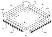
図12において、光源41Aは、4つの発光ダイオード411から構成されている。これら4つの発光ダイオード411は、同図に示すように、導光板42の四隅にほぼ対応するように均等に配置される。
このように、本発明において、光源として発光ダイオードを利用する場合における、その設置数は、基本的に自由に定められ得る事項である。現実にどの程度の個数の発光ダイオードを設けるかは、例えば、液晶装置LDの画面サイズ、要求される位置検出精度、等々を勘案して決められることになる(一般的にいって、画面サイズが大なら、発光ダイオードの数も多い方が好ましいと考えられる。)。In FIG. 12, the
Thus, in the present invention, when the light emitting diode is used as the light source, the number of the installed diodes is basically a matter that can be freely determined. The actual number of light emitting diodes to be provided is determined in consideration of, for example, the screen size of the liquid crystal device LD, the required position detection accuracy, and the like (in general, the screen size is If it is large, it is preferable that the number of light emitting diodes is large.)
図13においては、光源41Bは、2つの発光ダイオード411、及び、これらそれぞれに対応する2つの直方体状導光体412から構成されている。このうち直方体状導光体412は、基本的に、導光板42と本質的に同じ機能を果たす。すなわち、直方体状導光体412は、発光ダイオード411を発し該導光体412の端部から入射した光を、その内部に満たすのである。したがって、これは、導光板42と同様の材料(上述した)から作られて好適である。
ただし、この直方体状導光体412は、その一側面、即ち導光板42の側端面に対向する一側面から、光を出射する機能をもつ(図中符号“412a”参照)。この出射面412aは、そのような要求を満たすため、具体的には例えば、凹凸、あるいは、楔形断面をもつ微小な突起を所定方向に沿って並列させた構造等を備えて好適である。この場合更に、凹凸、あるいは突起の形成密度が、当該出射面412a内の位置に応じて、あるいは発光ダイオード411からの距離に応じて、変化させられること等により、当該出射面412a内における光射出効率を均一にする、等といった工夫が加えられてもよい。
あるいは、1個の直方体状導光体412の中で、前記出射面412aに対向する面には、場合により、例えばアルミニウム等の比較的高い光反射性能をもつ材料から作られる反射板が備えられてもよい。In FIG. 13, the
However, the rectangular parallelepiped
Alternatively, in one rectangular parallelepiped
図14において、光源41Cは、有機EL素子413EL及び導光体413から構成されている。
このうち導光体413は、少なくともその機能において、前述の直方体状導光体412と実質的に同じである。すなわち、導光体413は、有機EL素子413ELを出射した光をその内部に導入するとともに当該内部を当該光で満たし、かつ、その一側面から当該光を導光板42に向けて出射する。ただし、導光体413の場合は、その一側面上に有機EL素子413ELを形成可能とするために、その材料はガラスであることが好ましい。
他方、有機EL素子413ELは、この導光体413の一側面にあたかも貼り付けられるようにして形成されている。すなわち、有機EL素子413ELは、同図に示すように、反射電極413ELr、これに対向する透明電極413ELd、及び、これら両電極の間に挟持される発光機能層413ELoからなる積層構造をもつ。この有機EL素子413ELは、その透明電極413ELdが導光体413の一側面上に載るようにして、当該導光体413に直接的に形成されうる。
発光機能層413ELoには、反射電極413ELr及び透明電極413ELdそれぞれが所定の電位に設定されることにより、電流が流される。かかる電流の印加により、発光機能層18は発光する。発光機能層18を発した光は、直接、あるいは例えばアルミニウムやマグネシウム等で作られた反射電極413ELrで反射した後、例えばITO等で作られた透明電極413ELdを透過して導光体413の内部に導入される。
なお、これら導光体413及び有機EL素子413ELはいずれも、図14に示すように、導光板42の、ある一辺の長さに対応する長さをもつ。ただし、これら(特に、有機EL素子413EL)は、当該長さの方向に沿って、適当な数に分断されて形成されてよい。In FIG. 14, the
Among these, the
On the other hand, the organic EL element 413EL is formed so as to be attached to one side surface of the
A current flows through the light emitting functional layer 413ELo by setting each of the reflective electrode 413ELr and the transparent electrode 413ELd to a predetermined potential. By applying such a current, the light emitting functional layer 18 emits light. The light emitted from the light emitting functional layer 18 is reflected directly or after being reflected by a reflective electrode 413ELr made of, for example, aluminum or magnesium, and then transmitted through a transparent electrode 413ELd made of, for example, ITO. To be introduced.
Note that each of the
図15では、図14を参照して説明した光源41Cが、導光板42について4つある側端面(つまり、側端面の全部)に対応するように配置されている。 In FIG. 15, the
これら図14及び図15のように、光源41Cを有機EL素子413ELから構成する場合においては、上述した各実施形態に比べても、なお更に、当該光源41C及び導光板42を薄くすることが可能である。つまり、これらの形態では、画像品質の劣化のおそれを更に低減することが可能になるのである。
なお、有機EL素子を応用する形態に関する、その他のバリエーションについては、例えば特開平10−50124を参照されたい。本発明は、かかる文献に開示されるような光源をもまた、好適に利用可能である。
また、図15に示すような、いわば光源の四辺設置態様は、図12及び図13を参照して説明した光源41A及び41B、あるいは上記各実施形態の光源41についても同様に適用可能であることは言うまでもない。As shown in FIGS. 14 and 15, when the
For other variations regarding the form in which the organic EL element is applied, refer to, for example, JP-A-10-50124. The present invention can also suitably use a light source as disclosed in this document.
In addition, the four-sided installation mode of the light source as shown in FIG. 15 can be similarly applied to the
以上のように、本発明において採り得る光源の具体的態様は様々である。これらの各種態様のうちどれを選択するかは、上でも少し触れたように、液晶装置LDの画面サイズ、位置検出精度、材料コスト・製造コストの有利不利(例えば発光ダイオードの数が増えれば、光量の確保は容易だが、それだけコストは増加する。)、等々を勘案して決められる。 As described above, there are various specific modes of the light source that can be used in the present invention. As to which of these various aspects to select, as mentioned above, the screen size of the liquid crystal device LD, the position detection accuracy, the advantages and disadvantages of material cost and manufacturing cost (for example, if the number of light emitting diodes increases, It is easy to secure the amount of light, but the cost increases accordingly.)
ちなみに、光源(41,41A,41B,又は41C)から発せられる光強度が増大すれば、その散乱光(図7の散乱光SL1参照)の強度も増加することになるから、図6ないし図9を参照して説明した、外光LO、あるいは内光LIの影響を低減する効果がより実効的になるという傾向はある。したがって、光源の具体的態様をどのように構成するかを決めるにあたっては、このような事情を勘案することも極めて有意義である。
また、かかる事情は、ある特定の態様をとる光源(例えば、光源“41C”)を前提に、当該光源から発せられる光の強度をどの程度に設定するか(例えば、光源41Cなら、発光機能層413ELoにどの程度の大きさの電流を流すか)にあたっても、考慮されて好適である。
以上を要するに、本発明において、光源から発せられる光の強度は、所定値以上であることが好ましいということができる。Incidentally, if the intensity of light emitted from the light source (41, 41A, 41B, or 41C) increases, the intensity of the scattered light (see scattered light SL1 in FIG. 7) also increases. There is a tendency that the effect of reducing the influence of the external light LO or the internal light LI described with reference to is more effective. Therefore, it is very meaningful to take this situation into consideration when deciding how to configure the specific mode of the light source.
In addition, such a situation is based on the assumption that the intensity of light emitted from the light source is set on the premise of the light source (for example, the light source “41C”) taking a specific form (for example, if the
In short, in the present invention, it can be said that the intensity of light emitted from the light source is preferably a predetermined value or more.
(2) 上記各実施形態では、光検出素子15が、図1あるいは図2を参照して説明したように、1ピクセルごとに1個ずつ設けられているが、本発明は、かかる形態にも限定されない。光検出素子15の形成密度は、基本的に自由に設定され得る。一般的にいって、位置検出精度は、画像の分解能に比べて、より粗く設定することが可能であると考えられるから、光検出素子15は、図2との対比で言えば、より疎に形成することが可能である。例えば、ある画素行中の10ピクセルごとに、光検出素子を1個ずつ形成する等というようである(この場合、当該光検出素子を平面視した形状は、例えば、図2に比べてより長い長方形状となって好適である。)。
これによれば、実用上十分な位置検出精度を確保しながら、製造コスト等の低廉化を実現することができる。
あるいは、1ピクセルごとに1個ずつという場合よりも、より精細度が高まる形成密度(例えば、1“画素電極”ごとに1個の光検出素子)が採用されてもよい。(2) In each of the above embodiments, as described with reference to FIG. 1 or FIG. 2, one
According to this, it is possible to realize a reduction in manufacturing cost and the like while ensuring a practically sufficient position detection accuracy.
Alternatively, a formation density with higher definition (for example, one photodetecting element for each “pixel electrode”) may be employed than when one pixel is used for each pixel.
なお、これに関連して、本発明に係る「光検出素子」は、「複数」設けられて好適ではあるが、必ずしも、これが本発明の必要的要件になるわけではない。例えば、上述した、10ピクセルごとに1個の光検出素子の設置という例の場合、当該光検出素子は、これら10個のピクセルのうち両端のピクセル付近で発生した散乱光を受ける場合と、中央のピクセル付近で発生した散乱光を受ける場合とで、その発生する電流の大きさに相違を生じさせることが考えられる。これをうまく利用することができれば、場合によっては、1ピクセルごとに1個の光検出素子を設ける場合における位置検出精度と、それ程遜色のない精度による位置検出が行われる可能性がある。このような考え方を敷衍すれば、「光検出素子」は、絶対に、「複数」必要であるということにはならないのである(なお、そもそも「光検出素子」を何個設けるかは、画面サイズがどの程度であるか等その他の要因にもよる。)。
このようなことから、本発明においては、「光検出手段」が、「光検出素子」を究極的にいえば1個のみ含んでいる場合であっても、その範囲内に収める。特許請求の範囲において、「光検出手段は、複数の光検出素子」を含むとあっても、それは、「1個の光検出素子」を含む場合を積極的に排除するものではない。In this connection, it is preferable that “a plurality of” light detection elements according to the present invention be provided, but this is not necessarily a necessary requirement of the present invention. For example, in the case of the above-described example in which one photodetecting element is installed for every 10 pixels, the photodetecting element receives scattered light generated near the pixels at both ends of the ten pixels, and the center. It can be considered that the magnitude of the generated current is different from the case where the scattered light generated near the pixel is received. If this can be used successfully, in some cases, position detection may be performed with position detection accuracy in the case where one photodetecting element is provided for each pixel, and accuracy comparable to that. If this concept is used, it is not absolutely necessary that “photodetection elements” are “multiple” (in the first place, the number of “photodetection elements” depends on the screen size. It depends on other factors such as how much is.)
For this reason, in the present invention, even if the “photodetection means” includes only one “photodetection element” in the end, it falls within that range. In the claims, even though “the light detection means includes a plurality of light detection elements”, it does not actively exclude the case where “one light detection element” is included.
(3) また、上記各実施形態では、光検出素子15が、カラーフィルタCFとは無関係に、その検出面がいわば剥き出しになる状態で、第1基板10上に形成されているが、本発明は、これら光検出素子15及びカラーフィルタCFの関係を以下のように設定する態様も、その範囲内に収める。(3) Further, in each of the above embodiments, the
すなわち、図16及び図17において、光検出素子15は、第2基板20上に赤フィルタCF1と同時に形成された赤フィルタCF11に覆われるかのごとき状態におかれている。つまり、この赤フィルタCF11は、図2では遮光膜BM(図3参照)が形成されるべき領域の一部に形成されているということになる。これにより、光検出素子15には、赤色光のみが入射することになる。一方、この場合、光源41は、赤色光を発する発光ダイオード410から構成される。
このような形態によれば、図6ないし図9を参照して説明した外光LO、あるいは内光LIの影響はより低減する。なぜなら、一般に、外光LO、あるいは内光LIは、全波長領域の光を含んでいる(即ち、白色光である)ことが想定されるが、図16及び図17のような形態によれば、赤色光以外の光が光検出素子15に入射することが防止されることになるからである。つまり、光検出素子15が発生する電流の総量のうち、ノイズ成分としての外光LO及び内光LIによる寄与分が、相対的に減少するとみることができるのである。なお、位置検出にあたって重要な散乱光(図7の散乱光SL1)は、光源41から赤色光が発せられ、かつ、その赤色光は妨げられることなく光検出素子15に入射可能であるから、特に大きな問題なく検出可能である。
このように、図16及び図17に示す形態によれば、位置検出性能を貶めることなく、なお外光LO及び内光LIの影響を低減することができる。したがって、かかる形態では、上記各実施形態以上の正確な位置検出が可能性になる。That is, in FIGS. 16 and 17, the
According to such a form, the influence of the external light LO or the internal light LI described with reference to FIGS. 6 to 9 is further reduced. This is because, in general, the external light LO or the internal light LI is assumed to include light in the entire wavelength region (that is, white light). However, according to the configuration shown in FIGS. This is because light other than red light is prevented from entering the
As described above, according to the embodiments shown in FIGS. 16 and 17, the influence of the external light LO and the internal light LI can be reduced without giving up the position detection performance. Therefore, in this mode, it becomes possible to detect the position more accurately than in the above embodiments.
(4) 上記各実施形態では、導光板42の幅広面について何らかの要素を付加することについて特に説明していないが、本発明では、当該幅広面に、以下に述べるような様々な要素を備えさせることが可能である。
例えば、導光板42の幅広面には、光の反射を防止する反射防止膜が設けられてよい。この反射防止膜によれば、導光板42の表面における外光LOの反射を低減することができるので、外光LOの影響を受けない正確な位置検出という効果は、より確実に享受され得ることになる。同じことは、内光LIについても同様にいえる(即ち、導光板42の内部側の幅広面における反射が抑えられる。)。(4) In each of the above embodiments, there is no particular description about adding any element to the wide surface of the
For example, an antireflection film that prevents light reflection may be provided on the wide surface of the
あるいは、当該幅広面には、指の先の油脂等が導光板42に転写する、あるいは付着するのを防止する保護膜が設けられてもよい。また、かかる保護膜の設置に代えて又は加えて、当該幅広面には、付着した汚れの除去を容易にするための防汚処理を施してもよい。
あるいは更に、本発明は、当該幅広面に付着した汚れを検知する汚損検知手段と、その検知結果に基づいて、前記汚れの量が許容範囲を超えて存在する場合には、ユーザに対してその旨報知する報知手段とを併せ持つことにより、当該幅広面の清掃を一定期間ごとにユーザに促す機能を持たせてもよい。なお、この場合、前記汚損検知手段は、例えば、散乱光の異常発生を観測することを通じて汚れの位置及び程度を推定するものとして構成され得るし、あるいは、より端的に、パターン認識技術等を利用して汚れの位置及び程度を推定するものとして構成され得る。
以上述べたような形態によれば、導光板42の幅広面ないしその表面は、常に、一定程度以上の清浄さを保ち得ることになるから、例えば前記汚れ等による散乱光の発生等の不具合を被ることなく、位置検出の正確性は更に高まる。Alternatively, a protective film may be provided on the wide surface to prevent oil or fat at the tip of the finger from being transferred or adhered to the
Alternatively, the present invention provides a fouling detection means for detecting dirt adhering to the wide surface and, based on the detection result, when the amount of dirt is beyond an allowable range, In addition, a function for prompting the user to clean the wide surface at regular intervals may be provided by having a notification means for informing the user. In this case, the contamination detection means can be configured to estimate the position and degree of contamination by observing the occurrence of anomalies in scattered light, or more directly using pattern recognition technology or the like. Thus, it can be configured to estimate the position and degree of dirt.
According to the embodiment as described above, the wide surface of the
あるいは更に、これらの汚れ対策に代えて又は加えて、位置検出が、この汚れの存在をいわば織り込んだ上で行われるようにする形態も、本発明の範囲内にある。例えば、前記汚損検知手段により、定期的に、導光板42の幅広面上の汚れの存在位置を確認しておくとともに、位置検出の際には、当該汚れに起因する散乱光をノイズとして無視、あるいはキャンセルするのである。これによれば、汚れの存在にもかかわらず、位置検出をより正確に行うことができることとなる。 In addition, in place of or in addition to these countermeasures against contamination, a form in which position detection is performed after incorporating the presence of the contamination is also within the scope of the present invention. For example, the contamination detection means periodically confirms the presence position of dirt on the wide surface of the
(5) 上記第2実施形態では、本発明に係る「電気光学装置」が、もっぱら立体画像表示機能をもつ液晶表示装置に適用される例について説明しているが、本発明はかかる形態に限定されない。例えば、上述した液晶表示装置の構成及び駆動方法と殆ど同一の構成及び駆動方法をもつことで、二画像表示装置を構成することができる。ここでいう二画像表示装置とは、例えば、自動車のダッシュボードの中央に搭載されて好適な装置であり、これにより、運転席側に座る運転者にはある一の画像を、助手席側に座る同乗者にはそれとは別の画像を、それぞれ表示することが可能な装置である。この場合、図10あるいは図11における方向DRに進む光が運転席側の画像を、方向DAに進む光が助手席側の画像を、それぞれ構成する、といった運用を行うことになる。(5) In the second embodiment, an example in which the “electro-optical device” according to the present invention is applied exclusively to a liquid crystal display device having a stereoscopic image display function is described, but the present invention is limited to such a form. Not. For example, a two-image display device can be configured by having almost the same configuration and driving method as those of the liquid crystal display device described above. The two-image display device here is, for example, a device that is suitable for being mounted in the center of a dashboard of an automobile, whereby one image for a driver sitting on the driver's seat side is displayed on the passenger's seat side. It is a device that can display different images from the seated passengers. In this case, an operation is performed in which light traveling in the direction DR in FIG. 10 or FIG. 11 configures an image on the driver's seat side, and light traveling in the direction DA configures an image on the passenger seat side.
なお、本発明にいう「電気光学装置」とは、電気光学素子を備えることで、所定の画像を表示する機能を少なくとももつ装置をいう。ここで「電気光学素子」とは、電気信号(電流信号又は電圧信号)の供給によって透過率や輝度といった光学的特性が変化する素子である。具体的には例えば、上述した液晶素子や有機EL素子等がそれに該当する。この電気光学素子を適当な態様で複数配列し、かつ、これらを適当に制御することによって、前記所定の画像を表示することが可能となる。
また、本発明にいう「電気光学装置」は特に、いま述べた要素に加えて、上述したような「タッチパネル40」をその一具体例とする「タッチパネル」をその要素として含む用語として使用されている。The “electro-optical device” in the present invention refers to a device having at least a function of displaying a predetermined image by including an electro-optical element. Here, the “electro-optical element” is an element whose optical characteristics such as transmittance and luminance change when an electric signal (current signal or voltage signal) is supplied. Specifically, for example, the liquid crystal element and the organic EL element described above correspond to this. The predetermined image can be displayed by arranging a plurality of electro-optical elements in an appropriate manner and appropriately controlling them.
The “electro-optical device” according to the present invention is used in particular as a term including “touch panel” having the above-described “
<応用例>
次に、本発明に係る電気光学装置を利用した電子機器について説明する。図18ないし図21には、以上に説明した実施形態に係る液晶表示装置を採用した電子機器の形態が図示されている。<Application example>
Next, electronic equipment using the electro-optical device according to the invention will be described. 18 to 21 show forms of electronic devices that employ the liquid crystal display device according to the embodiment described above.
図18は、液晶表示装置を採用したモバイル型のパーソナルコンピュータの構成を示す斜視図である。パーソナルコンピュータ2000は、各種の画像を表示する液晶表示装置100と、電源スイッチ2001やキーボード2002が設置された本体部2010とを具備する。 FIG. 18 is a perspective view showing a configuration of a mobile personal computer employing a liquid crystal display device. The
図19は、液晶表示装置100を適用した携帯電話機の構成を示す斜視図である。携帯電話機3000は、複数の操作ボタン3001およびスクロールボタン3002と、各種の画像を表示する液晶表示装置100とを備える。スクロールボタン3002を操作することによって、液晶表示装置100に表示される画面がスクロールされる。 FIG. 19 is a perspective view illustrating a configuration of a mobile phone to which the liquid
図20は、液晶表示装置100を適用した携帯情報端末(PDA:Personal Digital Assistants)の構成を示す斜視図である。携帯情報端末4000は、複数の操作ボタン4001および電源スイッチ4002と、各種の画像を表示する液晶表示装置100とを備える。電源スイッチ4002を操作すると、住所録やスケジュール帳といった様々な情報が液晶表示装置100に表示される。 FIG. 20 is a perspective view showing a configuration of a personal digital assistant (PDA) to which the liquid
図21は、前述した、二画像表示装置を適用したカーナビゲーション装置の構成を示す図である。カーナビゲーション装置5000は、複数の操作ボタン5001と、各種の画像を表示する二画像表示装置1001とを備える。操作ボタン5001を操作すると、経路情報を含む道路地図や、渋滞情報、あるいは、お勧め観光スポット等の様々な情報(以下、「運行関連情報」という。)が二画像表示装置に表示される。
また、このカーナビゲーション装置5000では、二画像表示装置1001を利用して、DVD、ビデオテープ、あるいはテレビ受像信号等に基づく動画像等の表示を行うこともできる。
そして、このカーナビゲーション装置5000は、上述した二画像表示装置を搭載しているので、運転席5100に座る運転手に対して表示される画像と、助手席5200に座る同乗者に対して表示される画像とを異ならせることができる。この場合、好ましくは(特に、当該自動車の運行中には)、運転席5100の側に前記運行関連情報に係る画像が、助手席5200の側に前記動画像等が、それぞれ表示される。FIG. 21 is a diagram illustrating a configuration of the car navigation device to which the above-described two-image display device is applied. The
In the
Since the
なお、上述した図18乃至図21のいずれの場合においても、表示装置として、上記第2実施形態において説明した、立体画像表示機能をもつ液晶表示装置101又は102が適用されてよい。また、言うまでもないが、図21については、第1実施形態の液晶表示装置100が適用されてよく、さらに、図18乃至図20については、上述した二画像表示装置が適用されてよい。 In any of the cases of FIGS. 18 to 21 described above, the liquid
本発明に係る電気光学装置が適用される電子機器としては、図18から図21に例示した機器のほか、デジタルスチルカメラ、テレビ、ビデオカメラ、ページャ、電子手帳、電子ペーパー、電卓、ワードプロセッサ、ワークステーション、テレビ電話、POS端末、プリンタ、スキャナ、複写機、ビデオプレーヤ、タッチパネルを備えた機器等などが挙げられる。 As electronic apparatuses to which the electro-optical device according to the invention is applied, in addition to the apparatuses illustrated in FIGS. 18 to 21, a digital still camera, a television, a video camera, a pager, an electronic notebook, electronic paper, a calculator, a word processor, a work Examples include a station, a videophone, a POS terminal, a printer, a scanner, a copying machine, a video player, and a device equipped with a touch panel.
100,101,102……液晶表示装置、LB……照明装置、30U,30L……偏光板、LD……液晶装置、10……第1基板、9……画素電極、15……光検出素子、20……第2基板、CF……カラーフィルタ、CF1……赤フィルタ、CF2……緑フィルタ、CF3……青フィルタ、CF11……(光検出素子を覆うための)赤フィルタ、40……タッチパネル、41,41A,41B,41C……光源、42……導光板、410,411……発光ダイオード、412……直方体状導光体、412a……出射面、413……導光体、413EL……有機EL素子、413ELd……透明電極、413ELo……発光機能層、413ELr……反射電極、61……光学体、52……照明駆動回路、53……液晶駆動回路、54……位置検出回路、LO……外光、LI……内光、SL1……(光源出射光由来の)散乱光、SL2……(内光由来の)散乱光、FU……指100, 101, 102 ... Liquid crystal display device, LB ... Illumination device, 30U, 30L ... Polarizing plate, LD ... Liquid crystal device, 10 ... First substrate, 9 ... Pixel electrode, 15 ... Photodetection element , 20 ... second substrate, CF ... color filter, CF1 ... red filter, CF2 ... green filter, CF3 ... blue filter, CF11 ... red filter (to cover the light detection element), 40 ... Touch panel, 41, 41A, 41B, 41C... Light source, 42... Light guide plate, 410, 411. …… Organic EL element, 413ELd …… Transparent electrode, 413ELo …… Light emitting functional layer, 413ELr …… Reflective electrode, 61 …… Optical body, 52 …… Lighting drive circuit, 53 …… Liquid crystal drive circuit, 54 …… Position Detection circuit, LO ...... outside light, LI ...... internal light, SL1 ...... (from the light source emits light) scattered light, SL2 ...... (from internal light) scattered light, FU ...... finger
Claims (15)
Translated fromJapaneseその内部に前記光源から導入された光を、少なくともその幅広面で全反射する導光板と、
前記幅広面に接触した物体による、前記光に起因する散乱光を検出する光検出手段と、
前記光源の点灯時における前記光検出手段の出力と当該光源の消灯時における当該出力との差をとって前記散乱光の有無又は強度を検知することで、前記幅広面上における前記物体の接触位置を検出する位置検出手段と、
を備えることを特徴とするタッチパネル。A light source that repeatedly turns on and off;
A light guide plate that totally reflects light introduced from the light source therein at least on its wide surface;
Light detection means for detecting scattered light caused by the light by the object in contact with the wide surface;
By detecting the presence or absence or intensity of the scattered light by taking the difference between the output of the light detection means when the light source is turned on and the output when the light source is turned off, the contact position of the object on the wide surface Position detecting means for detecting
A touch panel comprising:
ことを特徴とする請求項1に記載のタッチパネル。The light source includes an organic EL element,
The touch panel according to claim 1.
ことを特徴とする請求項1又は2に記載のタッチパネル。An anti-reflection film provided to cover the wide surface;
The touch panel according to claim 1 or 2.
ことを特徴とする請求項1乃至3のいずれか一項に記載のタッチパネル。Further comprising an antifouling film for preventing dirt on the object from being transferred to the wide surface;
The touch panel according to claim 1, wherein the touch panel is provided.
前記位置検出手段は、
前記散乱光の有無又は強度を検知する際に、
前記汚損検知手段による検知結果に応じて、前記汚れに起因する撹乱散乱光の存在を無視する、
ことを特徴とする請求項1乃至4のいずれか一項に記載のタッチパネル。Further comprising a fouling detecting means for detecting dirt adhering to the wide surface;
The position detecting means includes
When detecting the presence or intensity of the scattered light,
Depending on the detection result by the contamination detection means, ignore the presence of disturbed scattered light due to the contamination,
The touch panel according to claim 1, wherein the touch panel is provided.
前記導光板の幅広面に略一致する面に、電気光学素子の光学的特性の変化に応じた画像を表示する画像表示装置と、
を備え、
前記画像表示装置は、
複数の画素電極が形成される第1基板と、
該第1基板に対向配置され、前記画素電極との間で所定の電位差を設定するための対向電極が形成される第2基板と、
これら第1基板及び第2基板間に挟持される電気光学物質と、
を含み、
前記導光板、前記第1基板及び前記第2基板は積層構造をとる、
ことを特徴とする電気光学装置。The touch panel according to any one of claims 1 to 5,
An image display device for displaying an image according to a change in the optical characteristics of the electro-optic element on a surface substantially coinciding with the wide surface of the light guide plate;
With
The image display device includes:
A first substrate on which a plurality of pixel electrodes are formed;
A second substrate disposed opposite to the first substrate and having a counter electrode for setting a predetermined potential difference with the pixel electrode;
An electro-optic material sandwiched between the first substrate and the second substrate;
Including
The light guide plate, the first substrate, and the second substrate have a laminated structure.
An electro-optical device.
前記光検出手段は、複数の光検出素子を含み、
前記複数の光検出素子は、
前記第1基板の上で、前記マトリクス状配列に応じた所定の配列に従って並ぶ、
ことを特徴とする請求項6に記載の電気光学装置。The plurality of pixel electrodes are arranged according to a matrix arrangement on the first substrate,
The light detection means includes a plurality of light detection elements,
The plurality of photodetecting elements are:
Arranged on the first substrate according to a predetermined arrangement according to the matrix arrangement,
The electro-optical device according to claim 6.
前記接触位置を検出するにあたり、
前記複数の光検出素子それぞれの前記第1基板上における配置位置を参照する、
ことを特徴とする請求項7に記載の電気光学装置。The position detecting means includes
In detecting the contact position,
Refer to the arrangement position of each of the plurality of light detection elements on the first substrate.
The electro-optical device according to claim 7.
前記カラーフィルタは、
前記光検出素子に係る前記所定の配列に対応する配列に従って並ぶ光検出素子用フィルタを含む、
ことを特徴とする請求項7又は8に記載の電気光学装置。A color filter arranged on the second substrate according to the arrangement corresponding to the matrix arrangement;
The color filter is
Including a light detection element filter arranged in accordance with an array corresponding to the predetermined array of the light detection elements,
The electro-optical device according to claim 7 or 8.
ことを特徴とする請求項9に記載の電気光学装置。The light source emits light of the same color as the color of the light detection element filter;
The electro-optical device according to claim 9.
当該電気光学装置は、
前記少なくとも2つの方向それぞれに対応する、少なくとも2つの表示範囲の各々に、画像を表示する、
ことを特徴とする請求項6乃至10のいずれか一項に記載の電気光学装置。Further comprising lens means for causing light emitted from or transmitted through the electro-optic material to travel along at least two different directions toward the light guide plate;
The electro-optical device is
Displaying an image in each of at least two display ranges corresponding to each of the at least two directions;
The electro-optical device according to any one of claims 6 to 10.
前記画素電極からみて、前記少なくとも2つの方向の各々に沿って延びる各直線全体が張る平面の法線方向に所定量ずらされた位置に形成される、
ことを特徴とする請求項11に記載の電気光学装置。The photodetecting element is
Each of the straight lines extending along each of the at least two directions as viewed from the pixel electrode is formed at a position shifted by a predetermined amount in the normal direction of the plane extending.
The electro-optical device according to claim 11.
前記画像表示装置は偏光板を更に含み、
当該偏光板は、前記レンズ手段に貼り付けられている、
ことを特徴とする請求項11又は12に記載の電気光学装置。The electro-optic material includes liquid crystal;
The image display device further includes a polarizing plate,
The polarizing plate is affixed to the lens means.
13. The electro-optical device according to claim 11 or 12,
前記画像を表示するためのフレーム周波数よりも大きい周波数で、点灯及び消灯を繰り返す、
ことを特徴とする請求項6乃至13のいずれか一項に記載の電気光学装置。The light source is
Repeat turning on and off at a frequency greater than the frame frequency for displaying the image,
The electro-optical device according to claim 6, wherein
ことを特徴とする電子機器。
The electro-optical device according to claim 6 is provided.
An electronic device characterized by that.
Priority Applications (1)
| Application Number | Priority Date | Filing Date | Title |
|---|---|---|---|
| JP2008027316AJP2009187342A (en) | 2008-02-07 | 2008-02-07 | Touch panel, electro-optical device and electronic apparatus |
Applications Claiming Priority (1)
| Application Number | Priority Date | Filing Date | Title |
|---|---|---|---|
| JP2008027316AJP2009187342A (en) | 2008-02-07 | 2008-02-07 | Touch panel, electro-optical device and electronic apparatus |
Publications (1)
| Publication Number | Publication Date |
|---|---|
| JP2009187342Atrue JP2009187342A (en) | 2009-08-20 |
Family
ID=41070507
Family Applications (1)
| Application Number | Title | Priority Date | Filing Date |
|---|---|---|---|
| JP2008027316APendingJP2009187342A (en) | 2008-02-07 | 2008-02-07 | Touch panel, electro-optical device and electronic apparatus |
Country Status (1)
| Country | Link |
|---|---|
| JP (1) | JP2009187342A (en) |
Cited By (13)
| Publication number | Priority date | Publication date | Assignee | Title |
|---|---|---|---|---|
| CN102200855A (en)* | 2010-03-24 | 2011-09-28 | 三星电子株式会社 | Object-sensing device |
| JP2011215904A (en)* | 2010-03-31 | 2011-10-27 | Casio Computer Co Ltd | Display device |
| JP2012008541A (en)* | 2010-05-28 | 2012-01-12 | Semiconductor Energy Lab Co Ltd | Photodetector |
| US8368677B2 (en) | 2010-03-31 | 2013-02-05 | Casio Computer Co., Ltd. | Optical sensor device, display apparatus, and method for driving optical sensor device |
| JP2013508851A (en)* | 2009-10-19 | 2013-03-07 | フラットフロッグ ラボラトリーズ アーベー | Touch surface with two-dimensional compensation |
| US8502772B2 (en) | 2010-07-02 | 2013-08-06 | Semiconductor Energy Laboratory Co., Ltd. | Driving method of input/output device |
| US8674972B2 (en) | 2010-09-08 | 2014-03-18 | Semiconductor Energy Laboratory Co., Ltd. | Semiconductor device |
| US8987651B2 (en) | 2010-10-07 | 2015-03-24 | Semiconductor Energy Laboratory Co., Ltd. | Photodetector including photodiodes overlapped with each other |
| US9200952B2 (en) | 2011-07-15 | 2015-12-01 | Semiconductor Energy Laboratory Co., Ltd. | Semiconductor device comprising a photodetector and an analog arithmetic circuit |
| US9390667B2 (en) | 2010-06-16 | 2016-07-12 | Semiconductor Energy Laboratory Co., Ltd. | Method for driving input-output device, and input-output device |
| US9459719B2 (en) | 2010-06-16 | 2016-10-04 | Semiconductor Energy Laboratory Co., Ltd. | Input-output device and method for driving the same |
| US9489088B2 (en) | 2010-06-16 | 2016-11-08 | Semiconductor Energy Laboratory Co., Ltd. | Input-output device and method for driving input-output device |
| US9946405B2 (en) | 2014-05-29 | 2018-04-17 | Semiconductor Energy Laboratory Co., Ltd. | Information processing device |
Citations (3)
| Publication number | Priority date | Publication date | Assignee | Title |
|---|---|---|---|---|
| JP2004318819A (en)* | 2003-03-31 | 2004-11-11 | Toshiba Matsushita Display Technology Co Ltd | Display device and information terminal device |
| JP2007506178A (en)* | 2003-09-22 | 2007-03-15 | コニンクリユケ フィリップス エレクトロニクス エヌ.ブイ. | Light touch screen |
| JP2007065508A (en)* | 2005-09-01 | 2007-03-15 | Sony Corp | Display device and display method |
- 2008
- 2008-02-07JPJP2008027316Apatent/JP2009187342A/enactivePending
Patent Citations (3)
| Publication number | Priority date | Publication date | Assignee | Title |
|---|---|---|---|---|
| JP2004318819A (en)* | 2003-03-31 | 2004-11-11 | Toshiba Matsushita Display Technology Co Ltd | Display device and information terminal device |
| JP2007506178A (en)* | 2003-09-22 | 2007-03-15 | コニンクリユケ フィリップス エレクトロニクス エヌ.ブイ. | Light touch screen |
| JP2007065508A (en)* | 2005-09-01 | 2007-03-15 | Sony Corp | Display device and display method |
Cited By (21)
| Publication number | Priority date | Publication date | Assignee | Title |
|---|---|---|---|---|
| JP2013508851A (en)* | 2009-10-19 | 2013-03-07 | フラットフロッグ ラボラトリーズ アーベー | Touch surface with two-dimensional compensation |
| KR101749266B1 (en)* | 2010-03-24 | 2017-07-04 | 삼성디스플레이 주식회사 | Touch sensing display device and cumputer-readable medium |
| JP2011204223A (en)* | 2010-03-24 | 2011-10-13 | Samsung Electronics Co Ltd | Touch sensing display |
| US9019238B2 (en) | 2010-03-24 | 2015-04-28 | Samsung Display Co., Ltd. | Object-sensing device |
| CN102200855A (en)* | 2010-03-24 | 2011-09-28 | 三星电子株式会社 | Object-sensing device |
| JP2011215904A (en)* | 2010-03-31 | 2011-10-27 | Casio Computer Co Ltd | Display device |
| US8368677B2 (en) | 2010-03-31 | 2013-02-05 | Casio Computer Co., Ltd. | Optical sensor device, display apparatus, and method for driving optical sensor device |
| KR101346456B1 (en) | 2010-03-31 | 2014-01-02 | 가시오게산키 가부시키가이샤 | Optical sensor device, display apparatus, and method for driving optical sensor device |
| US9846515B2 (en) | 2010-05-28 | 2017-12-19 | Semiconductor Energy Laboratory Co., Ltd. | Photodetector and display device with light guide configured to face photodetector circuit and reflect light from a source |
| US8772701B2 (en) | 2010-05-28 | 2014-07-08 | Semiconductor Energy Laboratory Co., Ltd. | Photodetector and display device with light guide configured to face photodetector circuit and reflect light from a source |
| JP2016192222A (en)* | 2010-05-28 | 2016-11-10 | 株式会社半導体エネルギー研究所 | Light detector and touch panel |
| JP2012008541A (en)* | 2010-05-28 | 2012-01-12 | Semiconductor Energy Lab Co Ltd | Photodetector |
| JP2015181022A (en)* | 2010-05-28 | 2015-10-15 | 株式会社半導体エネルギー研究所 | Light detector and touch panel |
| US9459719B2 (en) | 2010-06-16 | 2016-10-04 | Semiconductor Energy Laboratory Co., Ltd. | Input-output device and method for driving the same |
| US9390667B2 (en) | 2010-06-16 | 2016-07-12 | Semiconductor Energy Laboratory Co., Ltd. | Method for driving input-output device, and input-output device |
| US9489088B2 (en) | 2010-06-16 | 2016-11-08 | Semiconductor Energy Laboratory Co., Ltd. | Input-output device and method for driving input-output device |
| US8502772B2 (en) | 2010-07-02 | 2013-08-06 | Semiconductor Energy Laboratory Co., Ltd. | Driving method of input/output device |
| US8674972B2 (en) | 2010-09-08 | 2014-03-18 | Semiconductor Energy Laboratory Co., Ltd. | Semiconductor device |
| US8987651B2 (en) | 2010-10-07 | 2015-03-24 | Semiconductor Energy Laboratory Co., Ltd. | Photodetector including photodiodes overlapped with each other |
| US9200952B2 (en) | 2011-07-15 | 2015-12-01 | Semiconductor Energy Laboratory Co., Ltd. | Semiconductor device comprising a photodetector and an analog arithmetic circuit |
| US9946405B2 (en) | 2014-05-29 | 2018-04-17 | Semiconductor Energy Laboratory Co., Ltd. | Information processing device |
Similar Documents
| Publication | Publication Date | Title |
|---|---|---|
| JP2009187342A (en) | Touch panel, electro-optical device and electronic apparatus | |
| JP7349469B2 (en) | display device | |
| CN101997053B (en) | Photodetectors, Liquid Crystal Display Devices and Light Emitting Devices | |
| US8866797B2 (en) | Display device with position detecting function and electronic apparatus | |
| US8967847B2 (en) | Illumination assembly and display module | |
| KR101338114B1 (en) | Liquid crystal display device using Infrared Rays source and Multi Tourch System using the same | |
| JP4450089B2 (en) | Touch panel and electro-optical device | |
| JP2009116433A (en) | Electro-optical device with touch panel device and electronic apparatus | |
| JP2009134266A (en) | Display device and electronic device | |
| KR20090080487A (en) | Electro-optical devices, methods of manufacturing electro-optical devices, and electronic devices | |
| JP7123758B2 (en) | Electronics | |
| US11353647B2 (en) | Electronic device | |
| CN109725457B (en) | Backlight unit and liquid crystal display device including the same | |
| US20210263208A1 (en) | Display device | |
| US11988865B2 (en) | Display device | |
| JP2016071337A (en) | Display device | |
| JP2010056303A (en) | Optical sensor, and liquid crystal display using the same | |
| KR20130131147A (en) | Display device | |
| JP6131123B2 (en) | Display device with touch panel | |
| JP2014106428A (en) | Display device and electronic device | |
| JP2005043726A (en) | Display element and portable equipment using it | |
| KR20130010834A (en) | Display device | |
| US11041984B2 (en) | Display device and automobile | |
| US12147112B2 (en) | Transparent display apparatus for improving contrast ratio and manufacturing method | |
| JP6347987B2 (en) | Display device |
Legal Events
| Date | Code | Title | Description |
|---|---|---|---|
| A621 | Written request for application examination | Free format text:JAPANESE INTERMEDIATE CODE: A621 Effective date:20101208 | |
| A977 | Report on retrieval | Free format text:JAPANESE INTERMEDIATE CODE: A971007 Effective date:20111115 | |
| A131 | Notification of reasons for refusal | Free format text:JAPANESE INTERMEDIATE CODE: A131 Effective date:20111122 | |
| A521 | Written amendment | Free format text:JAPANESE INTERMEDIATE CODE: A523 Effective date:20120123 | |
| A02 | Decision of refusal | Free format text:JAPANESE INTERMEDIATE CODE: A02 Effective date:20120306 |