JP2009182343A - Wiring contact structure and manufacturing method thereof - Google Patents
Wiring contact structure and manufacturing method thereofDownload PDFInfo
- Publication number
- JP2009182343A JP2009182343AJP2009114497AJP2009114497AJP2009182343AJP 2009182343 AJP2009182343 AJP 2009182343AJP 2009114497 AJP2009114497 AJP 2009114497AJP 2009114497 AJP2009114497 AJP 2009114497AJP 2009182343 AJP2009182343 AJP 2009182343A
- Authority
- JP
- Japan
- Prior art keywords
- wiring
- film
- contact
- gate
- pattern
- Prior art date
- Legal status (The legal status is an assumption and is not a legal conclusion. Google has not performed a legal analysis and makes no representation as to the accuracy of the status listed.)
- Granted
Links
Images


Classifications
- G—PHYSICS
- G02—OPTICS
- G02F—OPTICAL DEVICES OR ARRANGEMENTS FOR THE CONTROL OF LIGHT BY MODIFICATION OF THE OPTICAL PROPERTIES OF THE MEDIA OF THE ELEMENTS INVOLVED THEREIN; NON-LINEAR OPTICS; FREQUENCY-CHANGING OF LIGHT; OPTICAL LOGIC ELEMENTS; OPTICAL ANALOGUE/DIGITAL CONVERTERS
- G02F1/00—Devices or arrangements for the control of the intensity, colour, phase, polarisation or direction of light arriving from an independent light source, e.g. switching, gating or modulating; Non-linear optics
- G02F1/01—Devices or arrangements for the control of the intensity, colour, phase, polarisation or direction of light arriving from an independent light source, e.g. switching, gating or modulating; Non-linear optics for the control of the intensity, phase, polarisation or colour
- G02F1/13—Devices or arrangements for the control of the intensity, colour, phase, polarisation or direction of light arriving from an independent light source, e.g. switching, gating or modulating; Non-linear optics for the control of the intensity, phase, polarisation or colour based on liquid crystals, e.g. single liquid crystal display cells
- G02F1/133—Constructional arrangements; Operation of liquid crystal cells; Circuit arrangements
- G02F1/1333—Constructional arrangements; Manufacturing methods
- G02F1/1345—Conductors connecting electrodes to cell terminals
- G02F1/13458—Terminal pads
- G—PHYSICS
- G02—OPTICS
- G02F—OPTICAL DEVICES OR ARRANGEMENTS FOR THE CONTROL OF LIGHT BY MODIFICATION OF THE OPTICAL PROPERTIES OF THE MEDIA OF THE ELEMENTS INVOLVED THEREIN; NON-LINEAR OPTICS; FREQUENCY-CHANGING OF LIGHT; OPTICAL LOGIC ELEMENTS; OPTICAL ANALOGUE/DIGITAL CONVERTERS
- G02F1/00—Devices or arrangements for the control of the intensity, colour, phase, polarisation or direction of light arriving from an independent light source, e.g. switching, gating or modulating; Non-linear optics
- G02F1/01—Devices or arrangements for the control of the intensity, colour, phase, polarisation or direction of light arriving from an independent light source, e.g. switching, gating or modulating; Non-linear optics for the control of the intensity, phase, polarisation or colour
- G02F1/13—Devices or arrangements for the control of the intensity, colour, phase, polarisation or direction of light arriving from an independent light source, e.g. switching, gating or modulating; Non-linear optics for the control of the intensity, phase, polarisation or colour based on liquid crystals, e.g. single liquid crystal display cells
- G02F1/133—Constructional arrangements; Operation of liquid crystal cells; Circuit arrangements
- G02F1/136—Liquid crystal cells structurally associated with a semi-conducting layer or substrate, e.g. cells forming part of an integrated circuit
- G02F1/1362—Active matrix addressed cells
- G02F1/136286—Wiring, e.g. gate line, drain line
- H—ELECTRICITY
- H10—SEMICONDUCTOR DEVICES; ELECTRIC SOLID-STATE DEVICES NOT OTHERWISE PROVIDED FOR
- H10D—INORGANIC ELECTRIC SEMICONDUCTOR DEVICES
- H10D86/00—Integrated devices formed in or on insulating or conducting substrates, e.g. formed in silicon-on-insulator [SOI] substrates or on stainless steel or glass substrates
- H10D86/40—Integrated devices formed in or on insulating or conducting substrates, e.g. formed in silicon-on-insulator [SOI] substrates or on stainless steel or glass substrates characterised by multiple TFTs
- H10D86/441—Interconnections, e.g. scanning lines
- H—ELECTRICITY
- H10—SEMICONDUCTOR DEVICES; ELECTRIC SOLID-STATE DEVICES NOT OTHERWISE PROVIDED FOR
- H10D—INORGANIC ELECTRIC SEMICONDUCTOR DEVICES
- H10D86/00—Integrated devices formed in or on insulating or conducting substrates, e.g. formed in silicon-on-insulator [SOI] substrates or on stainless steel or glass substrates
- H10D86/40—Integrated devices formed in or on insulating or conducting substrates, e.g. formed in silicon-on-insulator [SOI] substrates or on stainless steel or glass substrates characterised by multiple TFTs
- H10D86/60—Integrated devices formed in or on insulating or conducting substrates, e.g. formed in silicon-on-insulator [SOI] substrates or on stainless steel or glass substrates characterised by multiple TFTs wherein the TFTs are in active matrices
- G—PHYSICS
- G02—OPTICS
- G02F—OPTICAL DEVICES OR ARRANGEMENTS FOR THE CONTROL OF LIGHT BY MODIFICATION OF THE OPTICAL PROPERTIES OF THE MEDIA OF THE ELEMENTS INVOLVED THEREIN; NON-LINEAR OPTICS; FREQUENCY-CHANGING OF LIGHT; OPTICAL LOGIC ELEMENTS; OPTICAL ANALOGUE/DIGITAL CONVERTERS
- G02F1/00—Devices or arrangements for the control of the intensity, colour, phase, polarisation or direction of light arriving from an independent light source, e.g. switching, gating or modulating; Non-linear optics
- G02F1/01—Devices or arrangements for the control of the intensity, colour, phase, polarisation or direction of light arriving from an independent light source, e.g. switching, gating or modulating; Non-linear optics for the control of the intensity, phase, polarisation or colour
- G02F1/13—Devices or arrangements for the control of the intensity, colour, phase, polarisation or direction of light arriving from an independent light source, e.g. switching, gating or modulating; Non-linear optics for the control of the intensity, phase, polarisation or colour based on liquid crystals, e.g. single liquid crystal display cells
- G02F1/133—Constructional arrangements; Operation of liquid crystal cells; Circuit arrangements
- G02F1/136—Liquid crystal cells structurally associated with a semi-conducting layer or substrate, e.g. cells forming part of an integrated circuit
- G02F1/1362—Active matrix addressed cells
- G02F1/136227—Through-hole connection of the pixel electrode to the active element through an insulation layer
- G—PHYSICS
- G02—OPTICS
- G02F—OPTICAL DEVICES OR ARRANGEMENTS FOR THE CONTROL OF LIGHT BY MODIFICATION OF THE OPTICAL PROPERTIES OF THE MEDIA OF THE ELEMENTS INVOLVED THEREIN; NON-LINEAR OPTICS; FREQUENCY-CHANGING OF LIGHT; OPTICAL LOGIC ELEMENTS; OPTICAL ANALOGUE/DIGITAL CONVERTERS
- G02F1/00—Devices or arrangements for the control of the intensity, colour, phase, polarisation or direction of light arriving from an independent light source, e.g. switching, gating or modulating; Non-linear optics
- G02F1/01—Devices or arrangements for the control of the intensity, colour, phase, polarisation or direction of light arriving from an independent light source, e.g. switching, gating or modulating; Non-linear optics for the control of the intensity, phase, polarisation or colour
- G02F1/13—Devices or arrangements for the control of the intensity, colour, phase, polarisation or direction of light arriving from an independent light source, e.g. switching, gating or modulating; Non-linear optics for the control of the intensity, phase, polarisation or colour based on liquid crystals, e.g. single liquid crystal display cells
- G02F1/133—Constructional arrangements; Operation of liquid crystal cells; Circuit arrangements
- G02F1/136—Liquid crystal cells structurally associated with a semi-conducting layer or substrate, e.g. cells forming part of an integrated circuit
- G02F1/1362—Active matrix addressed cells
- G02F1/136286—Wiring, e.g. gate line, drain line
- G02F1/13629—Multilayer wirings
- H—ELECTRICITY
- H01—ELECTRIC ELEMENTS
- H01L—SEMICONDUCTOR DEVICES NOT COVERED BY CLASS H10
- H01L21/00—Processes or apparatus adapted for the manufacture or treatment of semiconductor or solid state devices or of parts thereof
- H01L21/70—Manufacture or treatment of devices consisting of a plurality of solid state components formed in or on a common substrate or of parts thereof; Manufacture of integrated circuit devices or of parts thereof
- H01L21/71—Manufacture of specific parts of devices defined in group H01L21/70
- H01L21/768—Applying interconnections to be used for carrying current between separate components within a device comprising conductors and dielectrics
- H01L21/76801—Applying interconnections to be used for carrying current between separate components within a device comprising conductors and dielectrics characterised by the formation and the after-treatment of the dielectrics, e.g. smoothing
- H01L21/76802—Applying interconnections to be used for carrying current between separate components within a device comprising conductors and dielectrics characterised by the formation and the after-treatment of the dielectrics, e.g. smoothing by forming openings in dielectrics
- H01L21/76805—Applying interconnections to be used for carrying current between separate components within a device comprising conductors and dielectrics characterised by the formation and the after-treatment of the dielectrics, e.g. smoothing by forming openings in dielectrics the opening being a via or contact hole penetrating the underlying conductor
- H—ELECTRICITY
- H01—ELECTRIC ELEMENTS
- H01L—SEMICONDUCTOR DEVICES NOT COVERED BY CLASS H10
- H01L21/00—Processes or apparatus adapted for the manufacture or treatment of semiconductor or solid state devices or of parts thereof
- H01L21/70—Manufacture or treatment of devices consisting of a plurality of solid state components formed in or on a common substrate or of parts thereof; Manufacture of integrated circuit devices or of parts thereof
- H01L21/71—Manufacture of specific parts of devices defined in group H01L21/70
- H01L21/768—Applying interconnections to be used for carrying current between separate components within a device comprising conductors and dielectrics
- H01L21/76801—Applying interconnections to be used for carrying current between separate components within a device comprising conductors and dielectrics characterised by the formation and the after-treatment of the dielectrics, e.g. smoothing
- H01L21/76802—Applying interconnections to be used for carrying current between separate components within a device comprising conductors and dielectrics characterised by the formation and the after-treatment of the dielectrics, e.g. smoothing by forming openings in dielectrics
- H01L21/76816—Aspects relating to the layout of the pattern or to the size of vias or trenches
- H—ELECTRICITY
- H01—ELECTRIC ELEMENTS
- H01L—SEMICONDUCTOR DEVICES NOT COVERED BY CLASS H10
- H01L23/00—Details of semiconductor or other solid state devices
- H01L23/52—Arrangements for conducting electric current within the device in operation from one component to another, i.e. interconnections, e.g. wires, lead frames
- H01L23/522—Arrangements for conducting electric current within the device in operation from one component to another, i.e. interconnections, e.g. wires, lead frames including external interconnections consisting of a multilayer structure of conductive and insulating layers inseparably formed on the semiconductor body
- H01L23/532—Arrangements for conducting electric current within the device in operation from one component to another, i.e. interconnections, e.g. wires, lead frames including external interconnections consisting of a multilayer structure of conductive and insulating layers inseparably formed on the semiconductor body characterised by the materials
- H01L23/53204—Conductive materials
- H01L23/53209—Conductive materials based on metals, e.g. alloys, metal silicides
- H01L23/53214—Conductive materials based on metals, e.g. alloys, metal silicides the principal metal being aluminium
- H01L23/53223—Additional layers associated with aluminium layers, e.g. adhesion, barrier, cladding layers
- H—ELECTRICITY
- H01—ELECTRIC ELEMENTS
- H01L—SEMICONDUCTOR DEVICES NOT COVERED BY CLASS H10
- H01L2924/00—Indexing scheme for arrangements or methods for connecting or disconnecting semiconductor or solid-state bodies as covered by H01L24/00
- H01L2924/0001—Technical content checked by a classifier
- H01L2924/0002—Not covered by any one of groups H01L24/00, H01L24/00 and H01L2224/00
Landscapes
- Physics & Mathematics (AREA)
- Nonlinear Science (AREA)
- Mathematical Physics (AREA)
- Chemical & Material Sciences (AREA)
- Crystallography & Structural Chemistry (AREA)
- General Physics & Mathematics (AREA)
- Optics & Photonics (AREA)
- Engineering & Computer Science (AREA)
- Microelectronics & Electronic Packaging (AREA)
- Thin Film Transistor (AREA)
- Liquid Crystal (AREA)
- Internal Circuitry In Semiconductor Integrated Circuit Devices (AREA)
- Electrodes Of Semiconductors (AREA)
Abstract
Translated fromJapaneseDescription
Translated fromJapanese本発明は、配線の接触構造及びその製造方法に関する。 The present invention relates to a wiring contact structure and a manufacturing method thereof.
一般に半導体装置の配線は信号を伝達する手段として用いられるため、信号遅延を最少化することが要求される。ここで、信号遅延を防止するために、配線は低抵抗を有する金属物質、特にアルミニウム(Al)やアルミニウム合金(Al alloy)などのようなアルミニウム系金属物質を使用することが一般的である。しかし、アルミニウムやアルミニウム合金の配線は物理的、化学的特性が脆いため、他の導電物質と連結される際に接触部で腐蝕が発生し、半導体素子の特性を低下させる問題がある。特に、液晶表示装置のように、透明な導電物質であるITOを使用して画素電極を形成する場合に、ITOとアルミニウムやアルミニウム合金の配線と接する接触部でアルミニウムやアルミニウム合金の配線が腐食する。このような問題を解決するために、ITOの代わりにアルミニウム系の配線と接しても腐蝕が発生しないIZOを画素電極として形成する技術が開発されているが、IZOの場合は接触部における接触抵抗が増加する問題がある。 In general, wiring of a semiconductor device is used as a means for transmitting a signal, so that it is required to minimize signal delay. Here, in order to prevent signal delay, the wiring generally uses a metal material having a low resistance, particularly an aluminum-based metal material such as aluminum (Al) or an aluminum alloy (Al alloy). However, since the wiring of aluminum or aluminum alloy is brittle in physical and chemical characteristics, there is a problem that corrosion occurs at the contact portion when it is connected to another conductive material, and the characteristics of the semiconductor element are deteriorated. In particular, when a pixel electrode is formed using ITO, which is a transparent conductive material, as in a liquid crystal display device, the aluminum or aluminum alloy wiring corrodes at the contact portion where the ITO contacts the aluminum or aluminum alloy wiring. . In order to solve such a problem, a technology has been developed for forming IZO as a pixel electrode that does not generate corrosion even when contacting with an aluminum-based wiring instead of ITO. In the case of IZO, the contact resistance at the contact portion is developed. There is a problem that increases.
本発明が目的とする技術的課題は、低抵抗物質からなると同時に低抵抗の接触特性を有する配線の接触構造及びその製造方法の提供にある。本発明の他の課題は、接触特性の良い配線の接触構造を含む薄膜トランジスタ基板及びその製造方法を提供することにある。 A technical problem to which the present invention is directed is to provide a contact structure of a wiring made of a low-resistance material and having low-resistance contact characteristics and a method for manufacturing the same. Another object of the present invention is to provide a thin film transistor substrate including a wiring contact structure with good contact characteristics and a method of manufacturing the same.
このような問題点を解決するために、本発明では、配線にアルミニウムやアルミニウム合金の導電膜を含めて形成し、接触部で接触孔を通じて側壁が露出されるように形成するか、または二重膜のうち一つに開口部を形成して他の膜を露出させる。この時、接触孔を通じて配線と連結されるIZOの導電層が、接触孔での段差によって断線しないように接触孔の境界線とこれと隣接した配線の境界線との間隔が2μm範囲を超えないことが好ましい。 In order to solve such a problem, in the present invention, the wiring is formed so as to include a conductive film of aluminum or an aluminum alloy, and the sidewall is exposed through the contact hole at the contact portion, or double An opening is formed in one of the films to expose the other film. At this time, the distance between the boundary line of the contact hole and the boundary line of the adjacent wiring does not exceed the 2 μm range so that the conductive layer of the IZO connected to the wiring through the contact hole does not break due to a step in the contact hole. It is preferable.
まず、本発明による配線の接触構造及びその製造方法において、基板上部に第1導電層により配線を形成し、その上部に絶縁膜を積層する。次に、絶縁膜をパターニングして配線の側壁を露出する接触孔を形成し、絶縁膜上に接触孔を通じて配線の側壁と接触する第2導電層を形成する。この時、第1導電層は低抵抗を有するアルミニウムやアルミニウム合金の上部膜と、IZOと低い接触抵抗を有するモリブデンやモリブデン合金またはクロムの下部膜とで形成されることが好ましい。第2導電層はIZOで形成することが好ましい。 First, in the wiring contact structure and the manufacturing method thereof according to the present invention, a wiring is formed on a substrate by a first conductive layer, and an insulating film is stacked on the wiring. Next, the insulating film is patterned to form contact holes that expose the side walls of the wiring, and a second conductive layer that contacts the side walls of the wiring through the contact holes is formed on the insulating film. At this time, the first conductive layer is preferably formed of an upper film of aluminum or aluminum alloy having low resistance and a lower film of molybdenum, molybdenum alloy or chromium having low contact resistance with IZO. The second conductive layer is preferably formed of IZO.
また、配線の外に位置する接触孔の境界線とこれと隣接した配線の境界線との間隔は2μm以内であるように接触孔を形成するのが好ましい。 Further, it is preferable that the contact hole is formed so that the distance between the boundary line of the contact hole located outside the wiring and the boundary line of the wiring adjacent thereto is within 2 μm.
また、本発明による他の配線の接触構造及びその製造方法において、基板上に開口部を有する配線を形成し、配線を覆う絶縁膜を積層する。次に、絶縁膜をパターニングして開口部を露出する接触孔を形成し、絶縁膜上に接触孔を通じて配線と接触する第1導電層を形成する。ここで、配線は、アルミニウムやアルミニウム合金の上部膜とモリブデンやモリブデン合金またはクロムの下部膜からなる第2導電層で形成し、第1導電層はIZOで形成するのが好ましい。この時、開口部は上部膜にのみ形成し、開口部は4μm×4μm以下の面積を有するように形成することが良い。 In another wiring contact structure and manufacturing method therefor according to the present invention, a wiring having an opening is formed on a substrate, and an insulating film covering the wiring is laminated. Next, the insulating film is patterned to form a contact hole that exposes the opening, and a first conductive layer that contacts the wiring through the contact hole is formed on the insulating film. Here, the wiring is preferably formed of an upper film of aluminum or an aluminum alloy and a second conductive layer made of a lower film of molybdenum, molybdenum alloy or chromium, and the first conductive layer is preferably formed of IZO. At this time, the opening is preferably formed only in the upper film, and the opening is preferably formed to have an area of 4 μm × 4 μm or less.
上部膜及び下部膜は、一つの感光膜パターンを用いた写真エッチング工程で形成できる。 The upper film and the lower film can be formed by a photolithography process using a single photosensitive film pattern.
このような本発明による配線の接触構造及びその製造方法は、薄膜トランジスタ基板及びその製造方法に適用することができる。 The wiring contact structure and the manufacturing method thereof according to the present invention can be applied to the thin film transistor substrate and the manufacturing method thereof.
本発明による薄膜トランジスタ基板には、絶縁基板上にゲート配線が形成されており、ゲート配線を覆うゲート絶縁膜及びその上に半導体層が形成されている。ゲート絶縁膜上にはデータ配線が形成され、その上部には半導体層を覆う保護膜が形成されている。ゲート絶縁膜または保護膜上には、少なくともゲート配線またはデータ配線の外に一部の境界線が位置し、ゲート配線またはデータ配線の側壁を露出するゲート絶縁膜または保護膜の第1接触孔を通じてゲート配線またはデータ配線の側壁と接触している透明導電膜パターンが形成されている。 In the thin film transistor substrate according to the present invention, a gate wiring is formed on an insulating substrate, a gate insulating film covering the gate wiring, and a semiconductor layer is formed thereon. A data wiring is formed on the gate insulating film, and a protective film covering the semiconductor layer is formed thereon. On the gate insulating film or the protective film, at least a part of the boundary line is located outside the gate wiring or the data wiring, and through the first contact hole of the gate insulating film or the protective film exposing the side wall of the gate wiring or the data wiring. A transparent conductive film pattern is formed in contact with the side walls of the gate wiring or data wiring.
ここで、ゲート配線またはデータ配線は、クロムまたはモリブデンやモリブデン合金の下部膜とアルミニウムやアルミニウム合金の上部膜からなり、ゲート絶縁膜及び保護膜は窒化ケイ素からなり、透明導電膜パターンはIZOからなることが好ましい。 Here, the gate wiring or the data wiring is made of a lower film of chromium, molybdenum or molybdenum alloy and an upper film of aluminum or aluminum alloy, the gate insulating film and the protective film are made of silicon nitride, and the transparent conductive film pattern is made of IZO. It is preferable.
ゲート配線は横方向に延びているゲート線、ゲート線と連結されているゲート電極及び外部から走査信号の伝達を受けてゲート線に伝達するゲートパッドを含み、データ配線は縦方向に延びているデータ線、データ線と連結されているソース電極、ソース電極と分離されゲート電極を中心にソース電極と対向し、第1接触孔を通じて側壁が露出されているドレーン電極及び外部から映像信号の伝達を受けてデータ線に伝達するデータパッドを含む。 The gate wiring includes a gate line extending in the horizontal direction, a gate electrode connected to the gate line, and a gate pad that receives a scanning signal from the outside and transmits the scanning signal to the gate line, and the data wiring extends in the vertical direction. A data line, a source electrode connected to the data line, a drain electrode separated from the source electrode, facing the source electrode with the gate electrode as the center, and a sidewall exposed through the first contact hole, and transmission of a video signal from the outside A data pad for receiving and transmitting to the data line.
この時、保護膜は、データパッドを露出する第2接触孔及びゲート絶縁膜と共にゲートパッドを露出させる第3接触孔を有し、第1乃至第3接触孔の大きさは4μm×4μm以上、10μm×10μm以下であるのが好ましい。透明導電膜パターンは、ドレーン電極の側壁と接触される。そして、画素電極は、第2及び第3接触孔を通じてデータパッド及びゲートパッドと各々連結されている補助データパッドまたは補助ゲートパッドと接触されている。この時、第2または第3接触孔では、データパッドまたはゲートパッドの側壁が露出されており、補助データパッドまたは補助ゲートパッドは少なくともデータパッド及びゲートパッドの側壁と接触されているのが好ましい。 At this time, the protective film has a second contact hole exposing the data pad and a third contact hole exposing the gate pad together with the gate insulating film, and the size of the first to third contact holes is 4 μm × 4 μm or more, It is preferably 10 μm × 10 μm or less. The transparent conductive film pattern is in contact with the sidewall of the drain electrode. The pixel electrode is in contact with the auxiliary data pad or the auxiliary gate pad connected to the data pad and the gate pad through the second and third contact holes. At this time, the side wall of the data pad or the gate pad is exposed in the second or third contact hole, and the auxiliary data pad or the auxiliary gate pad is preferably in contact with at least the side wall of the data pad and the gate pad.
このような本発明による薄膜トランジスタ基板の製造方法において、まず、絶縁基板上にゲート線、ゲート線と連結されているゲート電極を含むゲート配線を形成する。次に、ゲート配線を覆うゲート絶縁膜及びその上に半導体層を順次に形成し、ゲート線と交差するデータ線、データ線と連結され、ゲート電極に隣接するソース電極及びゲート電極に対してソース電極の対向側に位置するドレーン電極を含むデータ配線を形成する。次いで、保護膜を積層しパターニングして、少なくともドレーン電極の外に境界線が位置しドレーン電極の側壁を露出する第1接触孔を形成し、保護膜上に少なくともドレーン電極の側壁と接触する画素電極を形成する。 In such a method of manufacturing a thin film transistor substrate according to the present invention, first, a gate line including a gate line and a gate electrode connected to the gate line is formed on an insulating substrate. Next, a gate insulating film covering the gate wiring and a semiconductor layer are sequentially formed on the gate insulating film, and a data line crossing the gate line, a data line connected to the data line, and a source electrode adjacent to the gate electrode and a source with respect to the gate electrode A data wiring including a drain electrode located on the opposite side of the electrode is formed. Next, a protective film is stacked and patterned to form a first contact hole where a boundary line is located at least outside the drain electrode and exposes the side wall of the drain electrode, and a pixel that contacts at least the side wall of the drain electrode on the protective film An electrode is formed.
ここで、データ配線及び半導体層は、部分的に厚さが異なる感光膜パターンを用いた写真エッチング工程で共に形成でき、感光膜パターンは第1の厚さを有する第1部分、第1の厚さより厚い第2部分、厚さを有しない第3部分を含むことが好ましい。 Here, the data wiring and the semiconductor layer can be formed together by a photo etching process using a photosensitive film pattern having a partially different thickness, and the photosensitive film pattern includes a first portion having a first thickness, a first thickness. It is preferable to include a second portion that is thicker than the first portion and a third portion that does not have a thickness.
写真エッチング工程で感光膜パターンは、第1領域、第1領域より低い透過率を有する第2領域及び第1領域より高い透過率を有する第3領域を含む光マスクを用いて形成される。そして、写真エッチング工程において、第1部分はソース電極とドレーン電極との間、第2部分はデータ配線上に位置するように形成することが好ましい。 In the photoetching process, the photoresist pattern is formed using an optical mask including a first region, a second region having a lower transmittance than the first region, and a third region having a higher transmittance than the first region. In the photoetching process, it is preferable that the first portion is formed between the source electrode and the drain electrode and the second portion is positioned on the data wiring.
第1乃至第3領域の透過率を異ならせて調節するために、光マスクには半透明膜または露光器の分解能より小さいスリットパターンが形成されており、第1部分の厚さは第2部分の厚さに対して1/2以下にすることが好ましい。半導体層とデータ配線との間に抵抗性接触層を形成でき、データ配線と接触層及び半導体層を一つのマスクを用いて形成できる。 In order to adjust the transmittance of the first to third regions differently, a semi-transparent film or a slit pattern smaller than the resolution of the exposure device is formed on the optical mask, and the thickness of the first portion is the second portion. It is preferable to make it 1/2 or less with respect to the thickness. A resistive contact layer can be formed between the semiconductor layer and the data line, and the data line, the contact layer, and the semiconductor layer can be formed using one mask.
本発明によれば、接触部から配線の側壁傾斜面を露出させ、IZO膜との接触抵抗が低い導電膜とIZO膜とを接触させて、配線とIZO膜の接触抵抗を最少化し、接触部の信頼性を確保できる。また、低抵抗のアルミニウムやアルミニウム合金を含む導電膜を含む配線を形成することで、大画面、高精細の製品特性を向上させることができる。そして、製造工程を単純化して液晶表示装置用薄膜トランジスタ基板を製造するので、製造工程を単純化し、製造費用を削減できる。 According to the present invention, the sidewall inclined surface of the wiring is exposed from the contact portion, the conductive film having a low contact resistance with the IZO film is brought into contact with the IZO film, and the contact resistance between the wiring and the IZO film is minimized. Can be ensured. In addition, by forming a wiring including a conductive film containing low-resistance aluminum or aluminum alloy, it is possible to improve large-screen and high-definition product characteristics. And since a manufacturing process is simplified and the thin-film transistor substrate for liquid crystal display devices is manufactured, a manufacturing process can be simplified and manufacturing cost can be reduced.
添付した図面を参照して本発明の実施例よる配線の接触構造及びその製造方法と、これを含む薄膜トランジスタ基板及びその製造方法に対して本発明の属する技術分野における通常の知識を有する者が容易に実施できるように詳細に説明する。 Referring to the attached drawings, it is easy for a person having ordinary knowledge in the technical field to which the present invention relates to a wiring contact structure according to an embodiment of the present invention and a manufacturing method thereof, and a thin film transistor substrate including the same and a manufacturing method thereof. This will be described in detail so that it can be implemented.
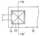
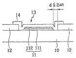
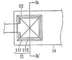
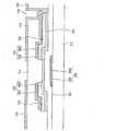
図1A乃至図3Eは、本発明の実施例に配線の接触構造を示した図面である。ここで、図1A、図2A、図2C及び図3A乃至図3Eは、配線の接触構造を示す配置図であり、図1B、図2B及び図2Dは、各々図1A、図2A及び図3CのIb-Ib’、IIb-IIb’及びIId-IId’線に沿った断面図である。 1A to 3E are views showing a contact structure of wiring in an embodiment of the present invention. Here, FIG. 1A, FIG. 2A, FIG. 2C, and FIG. 3A thru | or 3E are the layout views which show the contact structure of wiring, FIG. 1B, FIG. 2B and FIG. It is sectional drawing along the Ib-Ib ', IIb-IIb', and IId-IId 'line.
半導体装置、特に信号を伝達する配線として信号の遅延を最少化するためには、15μΩcm以下の低い比抵抗を有するアルミニウムやアルミニウム合金の金属物質が適する。この時、配線は外部から信号を受けたり、外部に信号を伝達するために他の導電層と連結されるが、製造過程で他の導電物質との接触抵抗が小さいことが要求される。このために、本発明の実施例による配線の接触構造製造方法では、図1A及び図1Bのように、基板10上にモリブデンやモリブデン合金またはクロムなどのようにIZOと低い接触抵抗を有する導電物質の下部膜111と、低抵抗を有するアルミニウムやアルミニウム合金からなる上部膜112を含む第1導電層11を積層しパターニングし、配線を形成し、配線11を覆う絶縁膜12を積層する。次に、絶縁膜12をパターニングして配線11を露出する接触孔13を形成し、絶縁膜12の上に接触孔13を通じて配線11と直接連結され、IZOからなる第2導電層14を形成する。この時、絶縁膜12の接触孔13は、配線11の側壁境界面、特に下部膜111の側壁境界面が十分露出されるように形成し、IZO膜14と下部膜111が十分に接するように接触部を形成する。ここで、接触孔13を通じて配線11と連結される第2導電層14が、接触孔13の段差または配線11下部のアンダーカット現象によって断線されることを防止できるように、接触孔13から露出された配線11の境界線とこれに隣接した接触孔13の境界線との間の間隔(d)が2μm範囲を超えないように接触孔13を形成することが好ましい。 In order to minimize signal delay as a semiconductor device, particularly as a signal transmission line, a metal material of aluminum or aluminum alloy having a low specific resistance of 15 μΩcm or less is suitable. At this time, the wiring is connected to another conductive layer in order to receive a signal from the outside or transmit the signal to the outside, but it is required that the contact resistance with the other conductive material is small in the manufacturing process. To this end, in the method for manufacturing a contact structure of a wiring according to an embodiment of the present invention, as shown in FIGS. 1A and 1B, a conductive material having a low contact resistance with IZO such as molybdenum, molybdenum alloy, or chromium on the
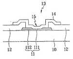
また、本発明の他の実施例による配線の接触構造及びその製造方法では、図2A及び図2Bのように、第1導電層の配線11の上部膜112に少なくとも一つ以上の開口部15を形成し、配線11を覆う絶縁膜12をパターニングし、開口部15を露出して接触孔13を形成する。次に、開口部15で配線11の下部膜111と接触する第2導電層14を形成する。この時、開口部15の面積は4×4μm以下で形成するのが好ましい。このように開口部15を小さく形成すれば、上部膜112と下部膜111を一つのマスクで形成できる。つまり、互いに異なるパターンの上部膜112と下部膜111をパターニングする時、まず写真エッチング工程で感光膜パターンをエッチングマスクとして、上部膜112を形成する。次いで、残った感光膜パターンまたは上部膜112をエッチングマスクとして下部膜111をエッチングする。この時、開口部15の面積は4×4μm以下と非常に小さいため、開口部15におけるエッチング速度が非常に遅く、下部膜111は完全に除去されず残る。こうして、互いに異なる模様の上部膜112と下部膜111を一つの感光膜パターンを用いる写真エッチング工程で形成できる。 In the wiring contact structure and the manufacturing method thereof according to another embodiment of the present invention, as shown in FIGS. 2A and 2B, at least one
さらに、本発明の他の実施例による配線の接触構造及びその製造方法において、下部膜111と第2導電層14の接触面積を確保するために、図2C及び図2Dのように、上部膜112の周囲外部に下部膜111の上部面が露出するように形成し、配線11の側面を階段構造に形成することもできる。この時、互いに異なるパターンの上部膜112と下部膜111を一つの感光膜パターンでパターニングする方法として、スリットパターンまたは半透明膜を用いたり、リフロー工程を用いて、周縁が他の部分より薄い配線用感光膜パターンを形成した後、二重でエッチングする方法が挙げられる。これに関しては、後に4枚マスクを用いた薄膜トランジスタアレイ基板の製造工程で具体的に説明する。 Furthermore, in the wiring contact structure and the manufacturing method thereof according to another embodiment of the present invention, in order to secure the contact area between the
一方、図3A乃至図3Dのように、配線11と接触孔13の誤整列マージンを有することができるように配線11または接触孔13を多様に変形でき、図3Eのように、配線11の開口部15を多数形成できる。 On the other hand, as shown in FIGS. 3A to 3D, the
このような配線の接触構造及びその製造方法は、液晶表示装置用薄膜トランジスタ及びその製造方法にも適用できる。 Such a wiring contact structure and a manufacturing method thereof can be applied to a thin film transistor for a liquid crystal display device and a manufacturing method thereof.
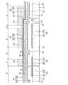
以下、このような本発明による配線の接触構造を含む液晶表示装置用薄膜トランジスタ基板及び製造方法について図面を参照して詳細に説明する。まず、図4及び図5を参照して本発明の第1の実施例による液晶表示装置用薄膜トランジスタ基板の構造について詳細に説明する。 Hereinafter, a thin film transistor substrate for a liquid crystal display device including a wiring contact structure according to the present invention and a manufacturing method thereof will be described in detail with reference to the drawings. First, the structure of the thin film transistor substrate for a liquid crystal display device according to the first embodiment of the present invention will be described in detail with reference to FIGS.
図4は、本発明の第1の実施例による液晶表示装置用薄膜トランジスタ基板であり、図5は、図4に示した薄膜トランジスタ基板のV-V’線に沿った断面図である。 4 is a thin film transistor substrate for a liquid crystal display device according to a first embodiment of the present invention, and FIG. 5 is a cross-sectional view taken along the line V-V ′ of the thin film transistor substrate shown in FIG. 4.
絶縁基板10上に、低抵抗を有するアルミニウムやアルミニウム合金の金属物質からなるゲート配線が形成されている。ゲート配線は横方向に延びているゲート線22、ゲート線22の端に連結され外部からのゲート信号の印加を受けてゲート線に伝達するゲートパッド24及びゲート線22に連結されている薄膜トランジスタのゲート電極26を含む。 On the insulating
基板10上には、窒化ケイ素(SiNx)などからなるゲート絶縁膜30がゲート配線22、24、26を覆っている。 A
ゲート電極26のゲート絶縁膜30上には、非晶質シリコンなどの半導体からなる半導体層40が島状に形成されており、半導体層40の上には、シリサイドまたはn型不純物が高濃度にドーピングされているn+水素化非晶質シリコンなどの物質で作られた抵抗接触層55、56が各々形成されている。 A
抵抗接触層55、56及びゲート絶縁膜30上には、アルミニウム(Al)やアルミニウム合金(Al alloy)、モリブデン(Mo)やモリブデン-タングステン(MoW)合金、クロム(Cr)、タンタル(Ta)、チタニウム(Ti)などの金属または導電体からなるデータ配線62、65、66、68が形成されている。データ配線は縦方向に形成され、ゲート線22と交差して画素領域を定義するデータ線62、データ線62に連結され抵抗接触層54の上部まで延びているソース電極65、データ線62の一端に連結され外部からの画像信号の印加を受けるデータパッド68、ソース電極65と分離されゲート電極26に対してソース電極65の反対側の抵抗接触層56上に形成されているドレーン電極66を含む。 On the resistive contact layers 55 and 56 and the
データ配線62、65、66、68は、アルミニウムやアルミニウム合金の単一膜で形成するのが好ましいが、二重層以上で形成しても良い。二重層以上で形成する場合には、一つの層は低抵抗物質で形成し、他の層は別の物質、特にIZOと低い接触抵抗を有する物質で作製することが好ましい。例として、Al(またはAl合金)/CrまたはAl(またはAl合金)/Mo(またはMo合金)などが挙げられ、本発明の実施例でデータ配線62、65、66、68は、クロムの下部膜601とアルミニウム-ネオジム合金の上部膜602の二重膜で形成されている。 The data wirings 62, 65, 66, and 68 are preferably formed of a single film of aluminum or aluminum alloy, but may be formed of a double layer or more. In the case of forming with two or more layers, it is preferable that one layer is formed of a low resistance material and the other layer is formed of another material, particularly a material having low contact resistance with IZO. Examples include Al (or Al alloy) / Cr or Al (or Al alloy) / Mo (or Mo alloy). In the embodiment of the present invention, the data wirings 62, 65, 66, and 68 are formed under the chromium. The
データ配線62、65、66、68及びこれらで覆われない半導体層40上には窒化ケイ素からなる保護膜70が形成されている。 A
保護膜70には、ドレーン電極66及びデータパッド68を各々露出する接触孔76、78が形成されており、ゲート絶縁膜30と共にゲートパッド24を露出する接触孔74が形成されている。ここで、接触孔76はドレーン電極66の境界線が露出されるように形成され、ドレーン電極68の下部膜601と上部膜602の側壁が全て接触孔76を通じて露出されている。この時、接触孔76及びデータ配線66は、図3A乃至図3Eのように様々な形になることができ、特にドレーン電極66を露出する接触孔76は10μm×10μm以下、4μm×4μm以上であるのが好ましい。また、パッド24、68を露出する接触孔74、78もパッドの境界線が露出されるように形成することができ、接触部の接触抵抗を最少化するために接触孔76より大きく形成することが好ましい。 Contact holes 76 and 78 for exposing the
保護膜70上には、接触孔76を通じてドレーン電極66と電気的に連結され画素に位置する画素電極82が形成されている。ここで、画素電極82は、接触孔76から露出されたドレーン電極66の側壁、特にドレーン電極66の下部膜601の側壁と十分に接触している。このような本発明の実施例による構造において、接触部の接触抵抗は良好なものと測定されている。これに関しては次の製造方法の記載で具体的に説明する。 A
また、保護膜70上には、接触孔74、78を通じて各々ゲートパッド24及びデータパッド68と連結されている補助ゲートパッド86及び補助データパッド88が形成されている。画素電極82と補助ゲート及びデータパッド86、88はIZOで形成されている。ここで、画素電極82は図4及び図5のように、ゲート線22と重なって維持蓄電器を構成し、保持容量が不足した場合にはゲート配線22、24、26と同一層に保持容量用配線を追加することもできる。 In addition, an
以下、このような本発明の第1の実施例による液晶表示装置用薄膜トランジスタ基板の製造方法について図4及び図5、図6A乃至図9Bを参照して詳細に説明する。 Hereinafter, a method of manufacturing a thin film transistor substrate for a liquid crystal display device according to the first embodiment of the present invention will be described in detail with reference to FIGS. 4 and 5 and FIGS. 6A to 9B.
まず、図6A及び6Bに示すように、基板10上に低抵抗を有するアルミニウムやアルミニウム合金のうち、2at%のNdを含むAl-Ndを含む標的を利用して2,500Å程度の膜厚に150℃程度でスパッタリングで積層しパターニングして、ゲート線22、ゲート電極26及びゲートパッド24を含み、テーパ構造を有する横方向のゲート配線を形成する。 First, as shown in FIGS. 6A and 6B, a film having a thickness of about 2,500 mm is obtained using a target containing Al—Nd containing 2 at% of Nd out of low-resistance aluminum or aluminum alloy on the
次に、図7A及び図7Bに示すように、窒化ケイ素からなるゲート絶縁膜30、非晶質シリコンからなる半導体層40、ドーピングされた非晶質シリコン層50の3層膜を連続積層し、マスクを用いたパターニング工程で半導体層40とドーピングされた非晶質シリコン層50をパターニングして、ゲート電極26と対向するゲート絶縁膜30上に半導体層40と抵抗接触層50を形成する。ここで、ゲート絶縁膜30は、窒化ケイ素を250〜400℃の温度範囲、2,000〜5,000Å程度の膜厚に積層して形成することが好ましい。 Next, as shown in FIGS. 7A and 7B, a three-layer film of a
次に、図8A乃至図8Bに示すように、モリブデンやモリブデン合金またはクロムなどからなる下部膜601を500Å程度の膜厚に、低抵抗を有するアルミニウムやアルミニウム合金のうち、2at%のNdを含むAl-Nd合金の標的を利用して上部膜602を150℃程度で2,500Å程度の膜厚さにスパッタリングで順次に積層する。その後、マスクを用いた写真工程でパターニングして、テーパ構造を有するデータ配線を形成する。データ配線としては、ゲート線22と交差するデータ線62、データ線62と連結されゲート電極26上部まで延びているソース電極65、データ線62は一側端に連結されているデータパッド68及びソース電極64と分離されており、ゲート電極26を中心にソース電極65と対向するドレーン電極66を含む。ここで、上部膜602及び下部膜601は、両方湿式エッチングでエッチングすることができる。また、上部膜602は湿式エッチングで、下部膜601は乾式エッチングでエッチングすることもでき、下部膜601がモリブデンやモリブデン合金膜である場合には、上部膜602と一つのエッチング条件でパターニングすることができる。また、ドレーン電極66の上部膜602にのみ開口部を形成し、最終的に図2A及び図2Bのような接触構造を形成することもできる。この開口部の面積を4μm×4μm以下と小さく形成し、マスクを用いる写真エッチング工程を別途追加しないことが好ましい。 Next, as shown in FIGS. 8A to 8B, the
そして、この後形成されるIZO膜と下部膜601とが十分に接触できるように下部膜601が上部膜602の下部にアンダーカットされることを防止することや、下部膜601が上部膜602の外に出るように形成することが好ましい。このために、モリブテンやモリブデン合金で下部膜601を形成する場合には、下部膜601と上部膜602の膜厚の比を1:5以上で積層し、DIPモードで実施して電池反応を最適化し、下部膜がアンダーカットされることを防止する。また、下部膜601をクロムで形成する場合には、下部膜601を500Å以下の膜厚さで積層し、洗浄工程または感光膜を除去する工程でアルミニウムやアルミニウム合金の上部膜602一部を除去する条件を適用し、クロムの下部膜601を上部膜602の外に出るように形成する。 Then, it is possible to prevent the
次に、データ配線62、65、66、68で覆われないドーピングされた非晶質シリコン層パターン50をエッチングしてゲート電極26を中心に両側に分離する一方、両側のドーピングされた非晶質シリコン層55、56の間の半導体層パターン40を露出させる。次いで、露出された半導体層40の表面を安定化するために酸素プラズマ処理を実施することが好ましい。 Next, the doped amorphous
次に、図9A及び図9Bのように、窒化ケイ素のような無機絶縁膜を250〜400℃の範囲で積層して保護膜70を形成し、マスクを用いた写真エッチング工程でゲート絶縁膜30と共に乾式エッチングでパターニングし、ゲートパッド24、ドレーン電極66及びデータパッド68を各々露出する接触孔74、76、78を形成する。ここで、接触孔74、76、78を形成する時のエッチング条件は、アルミニウムまたはアルミニウム合金の金属膜がエッチングされない条件を適用するのが好ましく、エッチング気体としてはF系の気体を使用できる。接触孔76は、ドレーン電極66の境界線及び上部膜601と下部膜601の側壁が露出されるように、また接触孔76からドレーン電極66の境界線が露出されるように形成する。この時、ドレーン電極66の外に位置する接触孔76の境界線とこれと隣接したドレーン電極66の境界線の間隔は、2μm以内の範囲になるように形成することが好ましい。これは、この後形成される画素電極82とドレーン電極66との間の接触抵抗を最少化し、接触孔76形成時にドレーン電極66の下部にアンダーカット現象が発生することを防止するためである。つまり、ドレーン電極66の外に位置する接触孔76の境界線とこれと隣接したドレーン電極66の境界線の間隔を3μm以上にして接触孔76を大きく形成すると、接触孔76を形成する時にドレーン電極66の下部でゲート絶縁膜30が過度にエッチングされ、アンダーカット現象が発生する。そうすると、ゲート絶縁膜30の段差によって、この後形成される画素電極82がドレーン電極66の下部で断線されるおそれがあり、これで接触部の接触抵抗が増加することになる。しかし、本発明の実施例のように、ドレーン電極66の外に位置する接触孔76の境界線と、これと隣接したドレーン電極66の境界線の間隔を2μm以内の範囲で接触孔76を形成すれば、ドレーン電極66の下部でゲート絶縁膜30が過度にエッチングされることなく、ドレーン電極66側壁の傾斜面を完全に露出させることができる。勿論、ここでパッド24、68を露出する接触孔74、78もパッド24、68の境界線が露出されるように形成し、図1A及び図1Bのように接触部を形成することもできる。 Next, as shown in FIGS. 9A and 9B, an inorganic insulating film such as silicon nitride is laminated at a temperature in the range of 250 to 400 ° C. to form the
最後に、図4及び5に示すように、IZO膜をスパッタリングで積層してマスクを用いたパターニングを実施し、接触孔76を通じてドレーン電極66と連結される画素電極82と接触孔74、78を通じてゲートパッド24及びデータパッド68と各々連結される補助ゲートパッド86及び補助データパッド88を各々形成する。この時、画素電極82は、ドレーン電極66の下部でアンダーカット現象が発生しないので断線されない。また、IZO膜と低い接触抵抗を有する下部膜601と十分に接しているので、接触部の接触抵抗を最少化することができる。本発明の実施例で、IZO膜82、86、88を形成するための標的は、出光(idemitsu)社のIDIXO(商品名:indium x-metal oxide)を使用し、標的はIn2O3及びZnOを含み、In+ZnでZnの含有量が15〜20at%の範囲であることが好ましい。また、IZO膜は、接触抵抗を最少化するために250℃以下の範囲で積層するのが好ましい。Finally, as shown in FIGS. 4 and 5, an IZO film is laminated by sputtering and patterning is performed using a mask, and the
このような本発明の実施例による製造工程で、画素の集合からなる表示領域の外の周辺領域に、画素領域に形成されている構造と同様なテストパターンで接触構造を形成し、接触部の接触抵抗を測定する。三つの場合に対してそれぞれ測定した。即ち、テストパターンは、接触孔76をドレーン電極66上に形成する第1の場合と、ドレーン電極66の外に位置する接触孔76の境界線とこれと隣接したドレーン電極66の境界線の間隔が3μm以上になるように接触孔を大きく形成する第2の場合、及び本発明の接触構造のようにドレーン電極66の外に位置する接触孔76の境界線とこれと隣接したドレーン電極66の境界線の間隔が2μm以内の範囲になるように形成する第3の場合に対するテストパターンを形成し、200個のテストパターンの接触抵抗を測定した。その結果、第1及び第2の場合は、接触抵抗がE7Ω以上と大きいものと測定されており、第3の場合はE6Ω以下と良好であった。 In the manufacturing process according to the embodiment of the present invention, a contact structure is formed in a peripheral area outside the display area composed of a set of pixels with a test pattern similar to the structure formed in the pixel area. Measure the contact resistance. Each of the three cases was measured. That is, the test pattern includes the first case where the
さらに、製造工程の時の様々な工程条件に対する接触部の接触抵抗をテストパターンを通じて測定した。 Furthermore, the contact resistance of the contact part with respect to various process conditions at the time of a manufacturing process was measured through the test pattern.
図10は、本発明の実施例による液晶表示装置用薄膜トランジスタ基板の周辺領域に形成されたテストパターンの接触抵抗を測定した結果を示す表である。 FIG. 10 is a table showing the results of measuring the contact resistance of the test pattern formed in the peripheral region of the thin film transistor substrate for a liquid crystal display device according to the embodiment of the present invention.
前記テストパターンは、表示領域の外の周辺部に形成し、図1A及び図1Bのようにデータ配線用金属層であるクロムの下部膜とアルミニウム合金の上部膜からなる配線、接触孔を有し窒化ケイ素からなる絶縁膜及びIZO膜からなる3層膜の構造に単純化し、200個の接触部を形成して接触抵抗を測定した。ここで、第1パターンは、接触孔の境界線が配線の上部にのみ位置するように接触部を形成しており、第2パターンは本発明の実施例のように配線側壁の傾斜面とIZO膜が接触するように接触部を形成している。絶縁膜は235℃、310℃の温度、2,000Å、3,000Åの膜厚の各々異なる条件で保護膜及びゲート絶縁膜を積層し、配線は150℃、50℃の温度で各々アルミニウム合金膜を積層する場合に対して接触抵抗を測定した。さらに、配線を1,500Å、3,000Åの抵抗性接触層をエッチングする気体に対して露出させた第1の場合と、63秒、68秒の間PEモードで絶縁膜をエッチングして接触孔を形成する第2の場合、1,000W、400WのICPモードで絶縁膜をエッチングして接触孔を形成する第3の場合、接触孔を通じて露出された配線を洗浄しない場合及び70秒間洗浄を行った第4の場合に対して各々接触抵抗を測定した。 The test pattern is formed in a peripheral portion outside the display area, and has wiring and contact holes made of a lower layer of chromium and an upper layer of aluminum alloy as a data wiring metal layer as shown in FIGS. 1A and 1B. Simplified into a structure of an insulating film made of silicon nitride and a three-layer film made of IZO film, 200 contact portions were formed, and contact resistance was measured. Here, the first pattern forms a contact portion so that the boundary line of the contact hole is located only at the upper part of the wiring, and the second pattern has an inclined surface of the wiring side wall and the IZO as in the embodiment of the present invention. A contact portion is formed so that the film contacts. The protective film and gate insulating film are laminated under different conditions of 235 ° C., 310 ° C., 2,000 ° C., and 3,000 ° C., and the wiring is made of an aluminum alloy film at temperatures of 150 ° C. and 50 ° C. The contact resistance was measured for the case of laminating. Further, in the first case where the wiring is exposed to the gas for etching the 1,500 mm and 3,000 mm resistive contact layer, the contact hole is formed by etching the insulating film in PE mode for 63 seconds and 68 seconds. In the second case where the contact hole is formed by etching the insulating film in the ICP mode of 1,000 W and 400 W, the case where the wiring exposed through the contact hole is not cleaned and the cleaning is performed for 70 seconds. The contact resistance was measured for each of the fourth cases.
図10に示すように、接触孔を10μm×10μmに形成した場合、第1のパターンの接触抵抗は5.3MΩ〜4.0GΩの範囲と大きく、第2のパターンの接触抵抗は14KΩ〜515KΩの範囲でE5Ω以下と良好なものと測定された。さらに、第1のパターンで接触抵抗が60KΩと良好に測定されたケースについて詳しく検討した結果、第1のパターンの接触構造が、第2のパターンの接触構造のように配線の境界線が接触孔から露出するように形成され、IZO膜と配線側壁、特に下部膜と十分に接触される構造であることが分かった。 As shown in FIG. 10, when the contact hole is formed to 10 μm × 10 μm, the contact resistance of the first pattern is as large as 5.3 MΩ to 4.0 GΩ, and the contact resistance of the second pattern is 14 KΩ to 515 KΩ. It was measured as good as E5Ω or less in the range. Furthermore, as a result of a detailed examination of the case where the contact resistance was measured as good as 60 KΩ in the first pattern, the contact structure of the first pattern is a contact hole of the wiring as in the contact structure of the second pattern. It was found that the structure is formed so as to be exposed from the IZO film, and is sufficiently in contact with the IZO film and the wiring side wall, particularly the lower film.
そして、接触孔を7μm×7μmに形成した場合は、第1のパターンの接触抵抗は12MΩ〜7.9GΩの範囲と大きく、第2のパターンの接触抵抗は18KΩ〜664KΩの範囲でE5Ω以下と良好なものと測定された。また、接触孔を4μm×4μmに形成した場合、第1のパターンの接触抵抗は48MΩ〜85GΩの範囲と大きく、第2のパターンの接触抵抗は30KΩ〜1.2MΩの範囲と良好な測定結果が出た。 When the contact hole is formed to 7 μm × 7 μm, the contact resistance of the first pattern is as large as 12 MΩ to 7.9 GΩ, and the contact resistance of the second pattern is as good as E5Ω or less in the range of 18 KΩ to 664 KΩ. It was measured. In addition, when the contact hole is formed to 4 μm × 4 μm, the contact resistance of the first pattern is as large as 48 MΩ to 85 GΩ, and the contact resistance of the second pattern is as high as 30 KΩ to 1.2 MΩ. I came out.
このような本発明の実施例による薄膜トランジスタアレイ基板の構造は、ゲート配線22、24、26及びデータ配線62、64、66、68が、低抵抗を有するアルミニウムやアルミニウム合金の導電膜を含むと同時に接触部、特にデータ配線とIZO膜の画素電極82の接触抵抗を最少化することができるので、大画面、高精細の液晶表示装置に適用することができる。 The structure of the thin film transistor array substrate according to the embodiment of the present invention is such that the gate wirings 22, 24, 26 and the data wirings 62, 64, 66, 68 include a low-resistance aluminum or aluminum alloy conductive film. Since the contact resistance between the contact portion, in particular, the data wiring and the
このような方法は、前述のように、5枚のマスクを用いる製造方法に適用できるが、4枚のマスクを用いる液晶表示装置用薄膜トランジスタ基板の製造方法にも同様に適用できる。これについて図面を参照して詳細に説明する。 Such a method can be applied to a manufacturing method using five masks as described above, but can be similarly applied to a manufacturing method of a thin film transistor substrate for a liquid crystal display device using four masks. This will be described in detail with reference to the drawings.
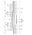
まず、図11乃至図13を参照して、本発明の実施例による4枚のマスクを用いて完成した液晶表示装置用薄膜トランジスタ基板の単位画素構造について詳細に説明する。図11は、本発明の第2の実施例による液晶表示装置用薄膜トランジスタ基板の配置図であり、図12及び図13は、各々図8に示す薄膜トランジスタ基板のXII-XII’線及びXIII-XIII’線に沿った断面図である。 First, a unit pixel structure of a thin film transistor substrate for a liquid crystal display device completed using four masks according to an embodiment of the present invention will be described in detail with reference to FIGS. FIG. 11 is a layout view of a thin film transistor substrate for a liquid crystal display according to a second embodiment of the present invention. FIGS. 12 and 13 are XII-XII ′ line and XIII-XIII ′ of the thin film transistor substrate shown in FIG. It is sectional drawing along a line.
絶縁基板10上には、第1の実施例と同様にアルミニウムまたはアルミニウム合金の低抵抗導電物質からなるゲート線22、ゲートパッド24及びゲート電極26を含むゲート配線が形成されている。そして、ゲート配線は、基板10上にゲート線22と平行し、上板の共通電極に入力される共通電極電圧などの電圧印加を外部から受ける維持電極28を含む。維持電極28は、後述する画素電極82と連結された維持蓄電器用導電体パターン68と重なり、画素の電荷保存能力を向上させる維持蓄電器を構成し、後述する画素電極82とゲート線22の重畳で発生する保持容量が十分な場合は形成しないこともある。 On the insulating
同様に、ゲート配線22、24、26、28は、アルミニウムやアルミニウム合金からなる単一層でも形成できるが、IZOと低い接触抵抗を有するクロムまたはモリブデンやモリブデン合金またはタンタルまたはチタニウムからなる下部膜201と、アルミニウムやアルミニウム合金からなる上部膜202を含む二重膜で形成されている。 Similarly, the gate wirings 22, 24, 26, and 28 can be formed of a single layer made of aluminum or aluminum alloy, but the
ゲート配線22、24、26、28上には、窒化ケイ素(SiNx)などからなるゲート絶縁膜30が形成され、ゲート配線22、24、26、28を覆っている。 A
ゲート絶縁膜30上には、水素化非晶質シリコンなどの半導体からなる半導体パターン42、48が形成されており、半導体パターン42、48上には、リン(P)などのn型不純物として高濃度でドーピングされている非晶質シリコンなどからなる抵抗性接触層パターンまたは中間層パターン55、56、58が形成されている。 On the
抵抗性接触層パターン55、56、58上には、低抵抗を有するアルミニウムやアルミニウム合金の導電物質からなる導電膜を含むデータ配線が形成されている。データ配線は、縦方向に形成されているデータ線62、データ線62の一端に連結され外部からの画像信号の印加を受けるデータパッド68、そしてデータ線62の分枝である薄膜トランジスタのソース電極65からなるデータ線部を含む。さらに、データ線部62、68、65と分離され、ゲート電極26または薄膜トランジスタのチャンネル部(C)に対してソース電極65の反対側に位置する薄膜トランジスタのドレーン電極66と維持電極28上に位置している維持蓄電器用導電体パターン64も含む。維持電極28を形成しない場合、維持蓄電器用導電体パターン64も形成しない。 On the resistive
データ配線62、64、65、66、68もゲート配線22、24、26、28と同様に、アルミニウムやアルミニウム合金の金属からなる単一層で形成できるが、第1の実施例と同様にクロムまたはモリブデンやモリブデン合金またはタンタルまたはチタニウムからなる下部膜601と、アルミニウムやアルミニウム合金からなる上部膜602を含む二重膜で形成されている。 The data lines 62, 64, 65, 66, and 68 can be formed of a single layer made of a metal such as aluminum or an aluminum alloy as in the case of the gate lines 22, 24, 26, and 28. It is formed of a double film including a
接触層パターン55、56、58は、その下部の半導体パターン42、48とその上部のデータ配線62、64、65、66、68の接触抵抗を小さくする役割をし、データ配線62、64、65、66、68と完全に同じ形態を有する。即ち、データ線部中間層パターン55はデータ線部62、68、65と同じであり、ドレーン電極用中間層パターン56はドレーン電極66と同じであり、維持蓄電器用中間層パターン58は維持蓄電器用導電体パターン64と同じである。 The
一方、半導体パターン42、48は、薄膜トランジスタのチャンネル部(C)を除けばデータ配線62、64、65、66、68及び抵抗性接触層パターン55、56、58と同じ形態である。具体的には、維持蓄電器用半導体パターン48と維持蓄電器用導電体パターン64及び維持蓄電器用接触層パターン58は同じ形態であるが、薄膜トランジスタ用半導体パターン42はデータ配線及び接触層パターンの他の部分と少し異なる。即ち、薄膜トランジスタのチャンネル部(C)でデータ線部62、68、65、特にソース電極65とドレーン電極66が分離されており、データ線部中間層55とドレーン電極用接触層パターン56も分離されているが、薄膜トランジスタ用半導体パターン42はここで切れることなく連結され、薄膜トランジスタのチャンネルを生成する。 On the other hand, the
データ配線62、64、65、66、68上には、窒化ケイ素からなる保護膜70が形成されている。保護膜70は、ドレーン電極66、データパッド68及び維持蓄電器用導電体パターン64を露出する接触孔76、78、72を有し、また、ゲート絶縁膜30と共にゲートパッド24を露出する接触孔74を有している。ここで、全ての接触孔72、74、76、78は、維持蓄電器用導電体パターン64、ゲートパッド24、ドレーン電極66、データパッド68の側壁、特にそれぞれのIZOと低い接触抵抗を有する下部膜201、601が露出するように形成されている。 A
保護膜70上には、薄膜トランジスタから画像信号を受けて上板の電極と共に電場を生成する画素電極82が形成されている。画素電極82は、IZOなどの透明な導電物質で形成され、接触孔76を通じてドレーン電極66と物理的・電気的に連結され画像信号の伝達を受ける。さらに、画素電極82は、隣接するゲート線22及びデータ線62と重なって開口率を高くしているが、重ならないこともある。また、画素電極82は、接触孔72を通じて維持蓄電器用導電体パターン64とも連結され導電体パターン64に画像信号を伝達する。一方、ゲートパッド24及びデータパッド68上には、接触孔74、78を通じて各々これらと連結される補助ゲートパッド86及び補助データパッド88が形成されており、これらはパッド24、68と外部回路装置との接着性を補完し、パッドを保護する役割をするもので必須ではなく、これらの適用の要否は選択的である。ここでも、接触部でIZO膜82、86、88は、維持蓄電器用導電体パターン64、ゲートパッド24、ドレーン電極66、データパッド68の側壁、特にIZOと低い接触抵抗を有する下部膜201、601と接触されている。 A
ここでは、画素電極82の材料の例として透明なIZOを挙げたが、透明な導電性ポリマーなどで形成することもでき、反射型液晶表示装置の場合、不透明な導電物質を用いても構わない。 Here, transparent IZO is given as an example of the material of the
以下、図11乃至図13の構造を有する液晶表示装置用薄膜トランジスタ基板を4枚のマスクを用いて製造する方法について図11乃至図13、図14A乃至図21Cを参照して詳細に説明する。 Hereinafter, a method for manufacturing a thin film transistor substrate for a liquid crystal display device having the structure of FIGS. 11 to 13 using four masks will be described in detail with reference to FIGS. 11 to 13 and FIGS. 14A to 21C.
まず、図14A乃至14Cに示したように、アルミニウムよりIZOと低い接触抵抗を有するモリブデンやモリブデン合金またはクロムなどからなる下部膜201と、低抵抗を有するアルミニウムやアルミニウム合金のうち、2at%のNdを含むAl-Nd合金の標的を利用して上部膜202をスパッタリングで順次に積層した後、1枚のマスクを用いた写真エッチング工程で基板10上にゲート線22、ゲートパッド24、ゲート電極26及び維持電極28を含むゲート配線をテーパ構造で形成する。ここでも、以後形成されるIZO膜と下部膜201とが十分に接触するように下部膜201が上部膜202の下部にアンダーカットされることを防止したり、下部膜が上部膜の外に出るように形成するのが好ましい。このために、モリブデンやモリブデン合金で下部膜201を形成する場合には、下部膜201と上部膜202の膜厚比を1:5以上に積層し、基板全体をエッチング液に浸してエッチングを行うDIPモードで電池反応を最適化し、下部膜がアンダーカットされることを防止する。また、下部膜201をクロムで形成する場合には、下部膜201を500Å以下の膜厚に積層し、洗浄工程または感光膜を除去する工程でアルミニウムやアルミニウム合金の上部膜202の一部を除去する条件を適用し、クロムの下部膜201が上部膜202の外に出るように形成する。 First, as shown in FIGS. 14A to 14C, a
次に、図15A及び15Bに示したように、窒化ケイ素からなるゲート絶縁膜30、半導体層40、中間層50を化学気相蒸着法を利用して各々1,500Å乃至5,000Å、500Å乃至2,000Å、300Å乃至600Åの膜厚に連続蒸着し、次いで低抵抗を有するアルミニウムやアルミニウム合金からなる上部膜601と、クロムまたはモリブデンやモリブデン合金からなる下部膜601を含む導電体層60をスパッタリングなどの方法で1,500Å乃至3,000Åの膜厚に蒸着した後、その上に感光膜110を1μm乃至2μmの膜厚に塗布する。 Next, as shown in FIGS. 15A and 15B, the
その後、第2マスクを通じて感光膜110に光を照射し現像して、図16B及び16Cに示したように、感光膜パターンの第2部分112、第1部分114を形成する。ここで、感光膜パターン112、114の中で薄膜トランジスタのチャンネル部(C)、つまり、ソース電極65とドレーン電極66の間に位置した第1部分114の厚さは、データ配線部(A)、つまり、データ配線62、64、65、66、68が形成される部分に位置した第2部分112の厚さより薄く形成し、その他の部分(B)の感光膜は全て取り除く。この時、チャンネル部(C)に残っている感光膜114の膜厚とデータ配線部(A)に残っている感光膜112の膜厚の比は後述するエッチング工程の工程条件によって異ならせる必要があり、第1部分114の厚さを第2部分112の厚さの1/2以下にするのが好ましく、例えば、4,000Å以下であることが好ましい。 Thereafter, the
このように、位置によって感光膜の膜厚を異ならせる方法としては様々なものがあり、A領域の光透過量を調節するために主にスリット(slit)や格子状のパターンを形成したり半透明膜を用いる。この時、スリットの間に位置したパターンの線幅やパターン間の間隔、即ちスリットの幅は、露光時使用する露光器の分解能より小さいのが好ましく、半透明膜を利用する場合には、マスク作製時に透過率を調節するために異なる透過率を有する薄膜を利用したり、異なる膜厚の薄膜を用いることができる。 As described above, there are various methods for changing the film thickness of the photosensitive film depending on the position. In order to adjust the light transmission amount in the area A, a slit or a lattice pattern is mainly formed. A transparent film is used. At this time, the line width of the pattern positioned between the slits and the interval between the patterns, that is, the width of the slit is preferably smaller than the resolution of the exposure device used at the time of exposure. In order to adjust the transmittance at the time of production, thin films having different transmittances can be used, or thin films having different film thicknesses can be used.
このようなマスクを通じて感光膜に光を照射すれば、光に直接露出される部分では高分子が完全分解され、スリットパターンや半透明膜が形成されている部分では光の照射量が少ないため高分子が不完全分解の状態となり、遮光膜で遮った部分では高分子がほとんど分解されない。次いで、感光膜を現像すると、分子が分解されなかった高分子部分だけが残され、照射光が少ない中央部分には光に全く照射されない部分より厚さの薄い感光膜を残すことができる。この時、露光時間を長くすれば全ての分子が分解されてしまうため、そうならないように注意する必要がある。 If the photosensitive film is irradiated with light through such a mask, the polymer is completely decomposed in the part exposed directly to the light, and the light irradiation amount is small in the part where the slit pattern or the translucent film is formed. The molecules are in an incompletely decomposed state, and the polymer is hardly decomposed at the portion blocked by the light shielding film. Next, when the photosensitive film is developed, only the polymer part where the molecules are not decomposed is left, and the photosensitive film having a thinner thickness than the part not irradiated with light can be left in the central part where the irradiation light is small. At this time, if the exposure time is increased, all molecules are decomposed, so care must be taken not to do so.
このような厚さの薄い感光膜114は、リフローが可能な物質からなる感光膜を用いて、光が完全に透過される部分と光が完全に透過されない部分に分けられた通常のマスクで露光した後、現像しリフローさせて感光膜が残留しない部分に感光膜の一部を流すことにより形成することもできる。 Such a thin
次に、感光膜パターン114及びその下部の膜など、即ち導電体層60、中間層50及び半導体層40に対するエッチングを行う。この時、データ配線部(A)にデータ配線及びその下部の膜などがそのまま残されることと、チャンネル部(C)に半導体層のみ残される必要があり、残りの部分(B)には前記三つの層である導電体層60、中間層50、半導体層40が全て除去され、ゲート絶縁膜30が露出されることが必要である。 Next, the
図14A及び14Bに示すように、その他の部分(B)の露出されている導電体層60を除去し、その下部の中間層50を露出させる。この過程では乾式エッチングや湿式エッチング方法を両方利用できる。この時、導電体層60はエッチングされ、感光膜パターン112、114はほとんどエッチングされない条件下で行うのが良い。しかし、乾式エッチングの場合、導電体層60のみをエッチングし、感光膜パターン112、114はエッチングされない条件を見つけ難いため、感光膜パターン112、114も一緒にエッチングされる条件下で行うこともできる。この場合には、湿式エッチングの場合より第1部分114の厚さを厚くし、この過程で感光膜パターンの第1部分114が除去され下部の導電体層60が露出されることがないようにする。 As shown in FIGS. 14A and 14B, the exposed
導電体層60がMoやMoW合金、AlやAl合金、Taのいずれかを含む場合には、乾式エッチングや湿式エッチングのいずれの方法でも良い。しかし、Crは乾式エッチングでは除去されないため、導電体層60がCrである場合は湿式エッチングのみを利用するのが良い。導電体層60がCrである湿式エッチングの場合には、エッチング液としてCeNHO3を使用でき、導電体層60がMoやMoWである乾式エッチングのエッチング気体としては、CF4とHClの混合気体やCF4とO2の混合気体を用いることができる。後者の場合、感光膜に対するエッチング比もほぼ同一である。When the
このようにすると、図17A及び図17Bに示すように、チャンネル部(C)及びデータ配線部(A)、(B)の導電体層、つまり、ソース/ドレーン用導電体パターン67と維持蓄電器用導電体パターン64だけ残され、その他の部分(B)の導電体層60は全て除去され、その下部の中間層50が露出される。残された導電体パターン67、64は、ソース及びドレーン電極65、66が分離されず連結されていることを除けば、データ配線62、64、65、66、68の形態と同一である。また、乾式エッチングを使用した場合、感光膜パターン112、114もある程度の厚さがエッチングされる。 In this way, as shown in FIGS. 17A and 17B, the conductor layers of the channel portion (C) and the data wiring portions (A) and (B), that is, the source /
図18A及び18Bに示すように、その他の部分(B)の露出された中間層50及びその下部の半導体層40を感光膜の第1部分114と共に乾式エッチング方法で同時に除去する。この時のエッチングは、感光膜パターン112、114と中間層50及び半導体層40(半導体層と中間層はエッチング選択性がほとんど無い)が同時にエッチングされ、ゲート絶縁膜30はエッチングされない条件下で行う必要がある。特に、感光膜パターン112、114と半導体層40に対するエッチング比がほとんど同一な条件下でエッチングすることが好ましい。例えば、SF6とHClの混合気体やSF6とO2の混合気体を使用すれば、ほとんど同一な膜厚に二つの膜をエッチングすることができる。感光膜パターン112、114と半導体層40に対するエッチング比が同一な場合、第1部分114の厚さは、半導体層40と中間層50の厚さを合せたものと同じであるか、それより小さい必要がある。As shown in FIGS. 18A and 18B, the exposed
このようにして、図18A及び18Bに示したように、チャンネル部(C)の第1部分114が除去されソース/ドレーン用導電体パターン67が露出され、その他の部分(B)の中間層50及び半導体層40が除去されその下部のゲート絶縁膜30が露出される。一方、データ配線部(A)の第2部分112もエッチングされるので厚さが薄くなる。そして、この工程で半導体パターン42、48が完成する。図面符号57と58は、各々ソース/ドレーン用導電体パターン67下部の中間層パターンと維持蓄電器用導電体パターン64下部の中間層パターンを示す。 In this way, as shown in FIGS. 18A and 18B, the
次いで、アッシング(ashing)を通じてチャンネル部(C)のソース/ドレーン用導電体パターン67表面の残留感光膜を除去する。 Next, the remaining photosensitive film on the surface of the source /
図19A及び19Bに示すように、チャンネル部(C)のソース/ドレーン用導電体パターン67及びその下部のソース/ドレーン用中間層パターン57をエッチングして除去する。この時、エッチングはソース/ドレーン用導電体パターン67及び中間層パターン57の両方に対して乾式エッチングのみで行うことができる。ソース/ドレーン用導電体パターン67に対しては湿式エッチングで、中間層パターン57に対しては乾式エッチングで行うこともできる。前者の場合、ソース/ドレーン用導電体パターン67及び中間層パターン57のエッチング選択比が大きい条件下でエッチングを行うことが好ましい。これは、エッチング選択比の大きくない場合、エッチング終了点を見つけ難くチャンネル部(C)に残る半導体パターン42の膜厚を調節することが容易ではないためである。例えば、SF6とO2の混合気体を用いてソース/ドレーン用導電体パターン67をエッチングする方法を挙げられる。湿式エッチングと乾式エッチングを入れ替えて行う後者の場合には、湿式エッチングされるソース/ドレーン用導電体パターン67の側面はエッチングされるが、乾式エッチングされる中間層パターン57はほとんどエッチングされないため階段状に形成される。中間層パターン57及び半導体パターン42のエッチング時に使用するエッチング気体の例としては、既に言及したCF4とHClの混合気体やCF4とO2の混合気体があり、CF4とO2を使用すれば、半導体パターン42を均一な膜厚に残すことができる。この時、図19Bに示すように、半導体パターン42の一部が除去され厚さが薄くなることもあり、感光膜パターンの第2部分112もこの時ある程度の厚さがエッチングされる。この時のエッチングはゲート絶縁膜30がエッチングされない条件で行う必要があり、第2部分112がエッチングされその下部のデータ配線62、64、65、66、68が露出されることがないように感光膜パターンの厚いことが良いのは勿論である。As shown in FIGS. 19A and 19B, the source /
このようにして、ソース電極65とドレーン電極66が分離されながらデータ配線62、64、65、66、68とその下部の接触層パターン55、56、58が完成する。 In this manner, the data wirings 62, 64, 65, 66, 68 and the
最後に、データ配線部(A)に残っている感光膜第2部分112を除去する。しかし、第2部分112の除去は、チャンネル部(C)ソース/ドレーン用導電体パターン67を除去した後、その下の中間層パターン57を除去する前に行われることもできる。 Finally, the second
前述のように、湿式エッチングと乾式エッチングを入れ替えて実施したり、乾式エッチングのみ用いることができる。後者の場合には、一種類のエッチングを使用するので工程が比較的に簡便であるが、適当なエッチング条件を見つけ出すことが難しい。前者の場合には、エッチング条件の検索は比較的に簡単であるが、後者に比べて工程が面倒な点がある。 As described above, wet etching and dry etching can be performed interchangeably, or only dry etching can be used. In the latter case, since one type of etching is used, the process is relatively simple, but it is difficult to find appropriate etching conditions. In the former case, the search of the etching conditions is relatively simple, but the process is troublesome compared to the latter.
このようにしてデータ配線62、64、65、66、68を形成した後、図20A及び図20Bに示す第1の実施例のように、窒化ケイ素をCVD方法で250〜400℃の範囲で蒸着して保護膜70を形成する。第3マスクを利用して保護膜70をゲート絶縁膜30と共にエッチングし、ドレーン電極66、ゲートパッド24、データパッド68及び維持蓄電器用導電体パターン64の下部膜201、601を各々露出する接触孔76、74、78、72を形成する。 After forming the data wirings 62, 64, 65, 66, and 68 in this way, silicon nitride is deposited in the range of 250 to 400 ° C. by the CVD method as in the first embodiment shown in FIGS. 20A and 20B. Thus, the
最後に、図11乃至図13のように、第1の実施例のような方法で厚さが400Å乃至500ÅであるIZO層をスパッタリング方法で蒸着し、第4マスクを使用してエッチングし、ドレーン電極66及び維持蓄電器用導電体パターン64と連結された画素電極82、ゲートパッド24と連結された補助ゲートパッド86及びデータパッド68と連結された補助データパッド88を形成する。IZOをパターニングするためのエッチング液は、クロム(Cr)の金属膜をエッチングするとき使用するクロムエッチング液を使用するが、これはアルミニウムを腐蝕させないので、データ配線とゲート配線が腐食することを防止できる。エッチング液として(HNO3/(NH4)2Ce(NO3)6/H2O)などが挙げられる。Finally, as shown in FIGS. 11 to 13, an IZO layer having a thickness of 400 to 500 mm is deposited by a sputtering method by the method as in the first embodiment, etched using a fourth mask, and drained. A
このような本発明の第2の実施例では、第1の実施例による効果だけでなく、さらに、データ配線62、64、65、66、68とその下部の接触層パターン55、56、58及び半導体パターン42、48を一つのマスクを用いて形成し、この過程でソース電極65とドレーン電極66が分離され、製造工程を単純化できる。 In the second embodiment of the present invention, not only the effects of the first embodiment but also the data wirings 62, 64, 65, 66, 68 and the
本発明の第1及び第2の実施例による液晶表示装置用薄膜トランジスタアレイ基板及びその製造方法では、図1A及び図1Bの接触構造を適用して説明したが、図2A乃至図3Eに示した接触構造も同様に適用できる。図1A乃至図3Eに示した接触構造は、他の半導体素子及びその製造方法に同様に適用できる。 The thin film transistor array substrate for a liquid crystal display device and the method of manufacturing the same according to the first and second embodiments of the present invention have been described by applying the contact structure of FIGS. 1A and 1B, but the contact shown in FIGS. 2A to 3E. The structure is applicable as well. The contact structure shown in FIGS. 1A to 3E can be similarly applied to other semiconductor elements and manufacturing methods thereof.
Claims (10)
Translated fromJapanese前記配線を覆う絶縁膜を積層する工程、
前記絶縁膜をパターニングし前記開口部を露出する接触孔を形成する工程、及び
前記絶縁膜上に前記接触孔を通じて前記配線と接触する第1導電層を形成する工程を含む配線の接触構造形成方法。Forming a wiring having an opening on a substrate;
Laminating an insulating film covering the wiring;
A method for forming a contact structure of a wiring, comprising: patterning the insulating film to form a contact hole exposing the opening; and forming a first conductive layer on the insulating film to contact the wiring through the contact hole .
前記配線を覆い、少なくとも前記開口部を露出する接触孔を有する絶縁膜、
前記絶縁膜上にIZOで形成され、前記接触孔及び前記開口部を通じて前記配線と接触している導電層を含む配線の接触構造。A wiring formed on the substrate and having an opening;
An insulating film covering the wiring and having a contact hole exposing at least the opening;
A wiring contact structure including a conductive layer formed of IZO on the insulating film and in contact with the wiring through the contact hole and the opening.
Applications Claiming Priority (2)
| Application Number | Priority Date | Filing Date | Title |
|---|---|---|---|
| KR2001/0022648 | 2001-04-26 | ||
| KR1020010022648AKR20020083249A (en) | 2001-04-26 | 2001-04-26 | A contact structure of a wires and method manufacturing the same, and thin film transistor substrate including the contact structure and method manufacturing the same |
Related Parent Applications (1)
| Application Number | Title | Priority Date | Filing Date |
|---|---|---|---|
| JP2002586379ADivisionJP4883878B2 (en) | 2001-04-26 | 2002-04-02 | Wiring contact structure, method of manufacturing the same, thin film transistor substrate including the same, and method of manufacturing the same |
Publications (2)
| Publication Number | Publication Date |
|---|---|
| JP2009182343Atrue JP2009182343A (en) | 2009-08-13 |
| JP5138633B2 JP5138633B2 (en) | 2013-02-06 |
Family
ID=19708759
Family Applications (2)
| Application Number | Title | Priority Date | Filing Date |
|---|---|---|---|
| JP2002586379AExpired - Fee RelatedJP4883878B2 (en) | 2001-04-26 | 2002-04-02 | Wiring contact structure, method of manufacturing the same, thin film transistor substrate including the same, and method of manufacturing the same |
| JP2009114497AExpired - Fee RelatedJP5138633B2 (en) | 2001-04-26 | 2009-05-11 | Method for manufacturing wiring contact structure |
Family Applications Before (1)
| Application Number | Title | Priority Date | Filing Date |
|---|---|---|---|
| JP2002586379AExpired - Fee RelatedJP4883878B2 (en) | 2001-04-26 | 2002-04-02 | Wiring contact structure, method of manufacturing the same, thin film transistor substrate including the same, and method of manufacturing the same |
Country Status (6)
| Country | Link |
|---|---|
| US (4) | US7303987B2 (en) |
| JP (2) | JP4883878B2 (en) |
| KR (1) | KR20020083249A (en) |
| CN (1) | CN100388506C (en) |
| AU (1) | AU2002246410A1 (en) |
| WO (1) | WO2002089177A2 (en) |
Cited By (5)
| Publication number | Priority date | Publication date | Assignee | Title |
|---|---|---|---|---|
| WO2012004958A1 (en)* | 2010-07-09 | 2012-01-12 | シャープ株式会社 | Thin-film transistor substrate, production method for same, and liquid crystal display panel |
| JP2012119664A (en)* | 2010-11-12 | 2012-06-21 | Kobe Steel Ltd | Wiring structure |
| JP2012138413A (en)* | 2010-12-24 | 2012-07-19 | Semiconductor Energy Lab Co Ltd | Formation method of opening and manufacturing method of semiconductor device |
| CN105158939A (en)* | 2015-09-14 | 2015-12-16 | 武汉华星光电技术有限公司 | Attaching method and assembly for backlight power supply welding disk and backlight golden finger |
| JP2020053694A (en)* | 2013-02-27 | 2020-04-02 | 株式会社半導体エネルギー研究所 | Semiconductor device |
Families Citing this family (38)
| Publication number | Priority date | Publication date | Assignee | Title |
|---|---|---|---|---|
| KR100796757B1 (en)* | 2001-11-29 | 2008-01-22 | 삼성전자주식회사 | Contact structure of the wiring and the thin film transistor substrate including the same |
| US7205570B2 (en) | 2002-07-19 | 2007-04-17 | Samsung Electronics Co., Ltd. | Thin film transistor array panel |
| KR100878238B1 (en)* | 2002-07-19 | 2009-01-13 | 삼성전자주식회사 | Thin film transistor array substrate and manufacturing method thereof |
| DE60336441D1 (en)* | 2002-09-02 | 2011-05-05 | Samsung Electronics Co Ltd | Contact structure for a semiconductor device, thin-layer transistor arrangement having such a contact structure and its production method |
| KR100872494B1 (en) | 2002-12-31 | 2008-12-05 | 엘지디스플레이 주식회사 | manufacturing method of array substrate for liquid crystal display device |
| KR100925458B1 (en) | 2003-01-17 | 2009-11-06 | 삼성전자주식회사 | Thin film transistor array panel and manufacturing method thereof |
| JP2004241774A (en)* | 2003-02-03 | 2004-08-26 | Samsung Electronics Co Ltd | Thin film transistor panel, method of manufacturing the same, and mask therefor |
| KR100947525B1 (en) | 2003-03-12 | 2010-03-12 | 삼성전자주식회사 | Thin film transistor substrate for liquid crystal display device and manufacturing method thereof |
| US7714820B2 (en) | 2003-06-27 | 2010-05-11 | Samsung Electronics Co., Ltd. | Contact structure of conductive films and thin film transistor array panel including the same |
| KR101039022B1 (en)* | 2004-02-11 | 2011-06-03 | 삼성전자주식회사 | Contact portion and manufacturing method thereof, thin film transistor array panel and manufacturing method thereof |
| KR101009677B1 (en)* | 2004-05-24 | 2011-01-19 | 엘지디스플레이 주식회사 | LCD and its manufacturing method |
| CN101044627B (en)* | 2004-09-15 | 2012-02-08 | 株式会社半导体能源研究所 | Semiconductor device |
| JP2006222386A (en)* | 2005-02-14 | 2006-08-24 | Toshiba Corp | Printed wiring boards, printed circuit boards, electronic equipment |
| JP4895102B2 (en) | 2005-06-09 | 2012-03-14 | 三星電子株式会社 | Thin film transistor display panel |
| KR20070003250A (en)* | 2005-07-01 | 2007-01-05 | 삼성전자주식회사 | Display device and manufacturing method thereof |
| EP1843194A1 (en) | 2006-04-06 | 2007-10-10 | Semiconductor Energy Laboratory Co., Ltd. | Liquid crystal display device, semiconductor device, and electronic appliance |
| KR100736576B1 (en)* | 2006-04-10 | 2007-07-06 | 엘지전자 주식회사 | Electroluminescent element and manufacturing method |
| TWI545380B (en) | 2006-05-16 | 2016-08-11 | 半導體能源研究所股份有限公司 | Liquid crystal display device and semiconductor device |
| US7847904B2 (en) | 2006-06-02 | 2010-12-07 | Semiconductor Energy Laboratory Co., Ltd. | Liquid crystal display device and electronic appliance |
| KR101499227B1 (en)* | 2008-08-20 | 2015-03-06 | 삼성디스플레이 주식회사 | Thin film transistor display panel and manufacturing method thereof |
| US8174021B2 (en)* | 2009-02-06 | 2012-05-08 | Semiconductor Energy Laboratory Co., Ltd. | Semiconductor device and method of manufacturing the semiconductor device |
| JP5271173B2 (en)* | 2009-06-26 | 2013-08-21 | 三菱電機株式会社 | Image display element and manufacturing method thereof |
| CN102034749B (en)* | 2009-09-25 | 2013-09-04 | 北京京东方光电科技有限公司 | Array substrate and manufacturing method thereof |
| TWM397596U (en)* | 2010-03-22 | 2011-02-01 | Mao Bang Electronic Co Ltd | Integrated circuit chip card |
| CN102844803B (en)* | 2010-04-22 | 2015-04-01 | 夏普株式会社 | Active matrix substrate and display device |
| KR101764902B1 (en) | 2010-12-06 | 2017-08-14 | 엘지디스플레이 주식회사 | Thin film Transistor substrate and method for manufacturing the same |
| TWI429985B (en)* | 2011-04-13 | 2014-03-11 | Au Optronics Corp | Lead structure and display panel having the same |
| TWI516851B (en)* | 2011-05-05 | 2016-01-11 | 友達光電股份有限公司 | Lead line structure of liquid crystal display panel and liquid crystal display panel having the same |
| CN102569416A (en)* | 2012-02-15 | 2012-07-11 | 华映光电股份有限公司 | Thin film transistor, thin film transistor substrate and production method thereof |
| JP2014081421A (en)* | 2012-10-15 | 2014-05-08 | Japan Display Inc | Wiring board and display device |
| KR102047004B1 (en)* | 2013-02-14 | 2019-11-21 | 삼성디스플레이 주식회사 | Organic light emitting display device and manufacturing method of the same |
| CN104241345B (en) | 2014-07-31 | 2017-11-28 | 京东方科技集团股份有限公司 | Aluminium electrode, the method and its electronic equipment for forming aluminium electrode |
| WO2016104216A1 (en)* | 2014-12-26 | 2016-06-30 | シャープ株式会社 | Semiconductor device, display device and method for manufacturing semiconductor device |
| CN106784015B (en)* | 2017-01-03 | 2019-12-03 | 京东方科技集团股份有限公司 | A kind of thin film transistor and its manufacturing method, display substrate and display device |
| CN109273483B (en)* | 2017-07-17 | 2021-04-02 | 京东方科技集团股份有限公司 | Display substrate, preparation method thereof, and display device |
| CN110211874B (en)* | 2019-05-13 | 2021-07-23 | 深圳市华星光电半导体显示技术有限公司 | Preparation method of thin film transistor and thin film transistor |
| CN114280863B (en)* | 2021-12-17 | 2024-04-12 | 滁州惠科光电科技有限公司 | Array substrate and display panel |
| CN119072116A (en)* | 2023-05-24 | 2024-12-03 | 长鑫存储技术有限公司 | Semiconductor structure and method for forming the same |
Citations (7)
| Publication number | Priority date | Publication date | Assignee | Title |
|---|---|---|---|---|
| JPS6235645A (en)* | 1985-08-09 | 1987-02-16 | Hitachi Ltd | Semiconductor devices and their manufacturing methods |
| JPH0222843A (en)* | 1988-07-11 | 1990-01-25 | Toshiba Corp | Semiconductor device |
| JPH08186174A (en)* | 1994-12-27 | 1996-07-16 | Nkk Corp | Wiring structure and method for forming the same |
| JPH1074834A (en)* | 1996-08-29 | 1998-03-17 | Nec Corp | Semiconductor device and manufacture thereof |
| JPH1126581A (en)* | 1997-07-07 | 1999-01-29 | Toshiba Corp | Semiconductor device and manufacturing method thereof |
| JPH11214504A (en)* | 1998-01-26 | 1999-08-06 | Mitsubishi Electric Corp | Semiconductor device and manufacturing method thereof |
| JP2001066639A (en)* | 1999-06-03 | 2001-03-16 | Samsung Electronics Co Ltd | Thin film transistor substrate for liquid crystal display device and method of manufacturing the same |
Family Cites Families (21)
| Publication number | Priority date | Publication date | Assignee | Title |
|---|---|---|---|---|
| KR0156178B1 (en)* | 1995-10-20 | 1998-11-16 | 구자홍 | Method for producing lcd device |
| KR0139346B1 (en)* | 1994-03-03 | 1998-06-15 | 김광호 | Manufacturing method of tft lcd |
| JPH0823028A (en)* | 1994-07-05 | 1996-01-23 | Oki Electric Ind Co Ltd | Semiconductor device having multilayer interconnect and manufacture thereof |
| JP3782194B2 (en)* | 1997-02-28 | 2006-06-07 | 株式会社東芝 | Active matrix liquid crystal display device |
| KR100262953B1 (en)* | 1997-06-11 | 2000-08-01 | 구본준 | Liquid crystal display device and manufacturing method of liquid crystal display device |
| KR100262954B1 (en)* | 1997-09-03 | 2000-08-01 | 구본준 | Liquid crystal display manufacturing method and structure by the manufacturing method |
| KR100316072B1 (en)* | 1997-12-10 | 2002-11-27 | 엘지.필립스 엘시디 주식회사 | Liquid crystal display and method of manufacturing the same |
| US6060714A (en)* | 1998-01-23 | 2000-05-09 | Ois Optical Imaging Systems, Inc. | Large area imager with photo-imageable interface barrier layer |
| JPH11337976A (en)* | 1998-03-26 | 1999-12-10 | Toshiba Corp | Array substrate for display device and flat display device provided with the array substrate |
| JP3463006B2 (en) | 1998-10-26 | 2003-11-05 | シャープ株式会社 | Method for manufacturing liquid crystal display device and liquid crystal display device |
| US6255130B1 (en)* | 1998-11-19 | 2001-07-03 | Samsung Electronics Co., Ltd. | Thin film transistor array panel and a method for manufacturing the same |
| JP2000330134A (en) | 1999-03-16 | 2000-11-30 | Furontekku:Kk | Thin film transistor substrate and liquid crystal display |
| KR100601170B1 (en) | 1999-04-26 | 2006-07-13 | 삼성전자주식회사 | Thin film transistor substrate for display device and manufacturing method thereof |
| US6218221B1 (en)* | 1999-05-27 | 2001-04-17 | Chi Mei Optoelectronics Corp. | Thin film transistor with a multi-metal structure and a method of manufacturing the same |
| US7411211B1 (en)* | 1999-07-22 | 2008-08-12 | Semiconductor Energy Laboratory Co., Ltd. | Contact structure and semiconductor device |
| KR100623979B1 (en)* | 1999-07-27 | 2006-09-13 | 삼성전자주식회사 | Liquid Crystal Display and Manufacturing Method Thereof |
| KR100333273B1 (en)* | 1999-08-02 | 2002-04-24 | 구본준, 론 위라하디락사 | The array substrate of TFT type liquid crystal display device and a method of fabricating the same |
| KR100646780B1 (en)* | 1999-08-12 | 2006-11-17 | 삼성전자주식회사 | Thin film transistor substrate for liquid crystal display device and manufacturing method thereof |
| KR100655276B1 (en)* | 1999-08-30 | 2006-12-08 | 삼성전자주식회사 | Thin film transistor liquid crystal display device and manufacturing method thereof |
| KR100366768B1 (en)* | 2000-04-19 | 2003-01-09 | 삼성전자 주식회사 | A contact portion of a wirings and method manufacturing the same, and thin film transistor substrate including the contact structure and method manufacturing the same |
| JP4342711B2 (en)* | 2000-09-20 | 2009-10-14 | 株式会社日立製作所 | Manufacturing method of liquid crystal display device |
- 2001
- 2001-04-26KRKR1020010022648Apatent/KR20020083249A/ennot_activeCeased
- 2002
- 2002-04-02JPJP2002586379Apatent/JP4883878B2/ennot_activeExpired - Fee Related
- 2002-04-02CNCNB028126904Apatent/CN100388506C/ennot_activeExpired - Lifetime
- 2002-04-02WOPCT/KR2002/000582patent/WO2002089177A2/ennot_activeCeased
- 2002-04-02AUAU2002246410Apatent/AU2002246410A1/ennot_activeAbandoned
- 2002-04-02USUS10/475,903patent/US7303987B2/ennot_activeExpired - Lifetime
- 2007
- 2007-11-29USUS11/947,204patent/US20080090404A1/ennot_activeAbandoned
- 2008
- 2008-12-12USUS12/333,973patent/US7659625B2/ennot_activeExpired - Lifetime
- 2009
- 2009-05-11JPJP2009114497Apatent/JP5138633B2/ennot_activeExpired - Fee Related
- 2009-12-22USUS12/645,458patent/US20100096176A1/ennot_activeAbandoned
Patent Citations (7)
| Publication number | Priority date | Publication date | Assignee | Title |
|---|---|---|---|---|
| JPS6235645A (en)* | 1985-08-09 | 1987-02-16 | Hitachi Ltd | Semiconductor devices and their manufacturing methods |
| JPH0222843A (en)* | 1988-07-11 | 1990-01-25 | Toshiba Corp | Semiconductor device |
| JPH08186174A (en)* | 1994-12-27 | 1996-07-16 | Nkk Corp | Wiring structure and method for forming the same |
| JPH1074834A (en)* | 1996-08-29 | 1998-03-17 | Nec Corp | Semiconductor device and manufacture thereof |
| JPH1126581A (en)* | 1997-07-07 | 1999-01-29 | Toshiba Corp | Semiconductor device and manufacturing method thereof |
| JPH11214504A (en)* | 1998-01-26 | 1999-08-06 | Mitsubishi Electric Corp | Semiconductor device and manufacturing method thereof |
| JP2001066639A (en)* | 1999-06-03 | 2001-03-16 | Samsung Electronics Co Ltd | Thin film transistor substrate for liquid crystal display device and method of manufacturing the same |
Cited By (9)
| Publication number | Priority date | Publication date | Assignee | Title |
|---|---|---|---|---|
| WO2012004958A1 (en)* | 2010-07-09 | 2012-01-12 | シャープ株式会社 | Thin-film transistor substrate, production method for same, and liquid crystal display panel |
| JP5269253B2 (en)* | 2010-07-09 | 2013-08-21 | シャープ株式会社 | Method for manufacturing thin film transistor substrate |
| US8623681B2 (en) | 2010-07-09 | 2014-01-07 | Sharp Kabushiki Kaisha | Thin film transistor substrate, method for manufacturing the same, and liquid crystal display panel |
| KR101356304B1 (en)* | 2010-07-09 | 2014-01-28 | 샤프 가부시키가이샤 | Production method for thin-film transistor substrate |
| JP2012119664A (en)* | 2010-11-12 | 2012-06-21 | Kobe Steel Ltd | Wiring structure |
| JP2012138413A (en)* | 2010-12-24 | 2012-07-19 | Semiconductor Energy Lab Co Ltd | Formation method of opening and manufacturing method of semiconductor device |
| JP2020053694A (en)* | 2013-02-27 | 2020-04-02 | 株式会社半導体エネルギー研究所 | Semiconductor device |
| CN105158939A (en)* | 2015-09-14 | 2015-12-16 | 武汉华星光电技术有限公司 | Attaching method and assembly for backlight power supply welding disk and backlight golden finger |
| CN105158939B (en)* | 2015-09-14 | 2019-02-22 | 武汉华星光电技术有限公司 | A kind of applying method and component of backlight power supply pad and backlight golden finger |
Also Published As
| Publication number | Publication date |
|---|---|
| CN1628389A (en) | 2005-06-15 |
| US7659625B2 (en) | 2010-02-09 |
| KR20020083249A (en) | 2002-11-02 |
| WO2002089177A3 (en) | 2003-03-13 |
| CN100388506C (en) | 2008-05-14 |
| JP5138633B2 (en) | 2013-02-06 |
| JP2005506683A (en) | 2005-03-03 |
| US20100096176A1 (en) | 2010-04-22 |
| US20040238825A1 (en) | 2004-12-02 |
| US20090096105A1 (en) | 2009-04-16 |
| JP4883878B2 (en) | 2012-02-22 |
| WO2002089177A2 (en) | 2002-11-07 |
| US20080090404A1 (en) | 2008-04-17 |
| AU2002246410A1 (en) | 2002-11-11 |
| US7303987B2 (en) | 2007-12-04 |
Similar Documents
| Publication | Publication Date | Title |
|---|---|---|
| JP5138633B2 (en) | Method for manufacturing wiring contact structure | |
| JP4928665B2 (en) | Wiring contact structure, method for forming the same, thin film transistor substrate including the same, and method for manufacturing the same | |
| JP4801828B2 (en) | Method for manufacturing thin film transistor substrate for liquid crystal display device | |
| JP4790134B2 (en) | Method for manufacturing thin film transistor substrate for liquid crystal display device | |
| JP4373789B2 (en) | Wiring structure, thin film transistor substrate using the same, and manufacturing method thereof | |
| US7666697B2 (en) | Thin film transistor substrate and method of manufacturing the same | |
| US7649581B2 (en) | Array substrate of an LCD comprising first and second gate insulating layers and method of fabricating the same | |
| JP2005510064A (en) | Contact portion of semiconductor element and manufacturing method thereof, thin film transistor array substrate for liquid crystal display device including the same, and manufacturing method thereof | |
| KR100372306B1 (en) | Manufacturing Method of Thin Film Transistor | |
| JP2004226975A (en) | Thin film transistor panel and method of manufacturing the same | |
| JP2001358343A (en) | Wiring contact structure, method of forming the same, thin film transistor substrate including the same, and method of manufacturing the same | |
| JP4996789B2 (en) | Method for forming wiring contact structure and method for manufacturing thin film transistor substrate | |
| KR100864490B1 (en) | The contact portion of the wiring and the thin film transistor substrate including the same | |
| KR100750914B1 (en) | Transparent conductive film for pixel electrode, thin film transistor substrate for liquid crystal display including the same, and manufacturing method thereof | |
| KR100750913B1 (en) | Method for manufacturing wiring and thin film transistor substrate for liquid crystal display device including the wiring and method for manufacturing same | |
| KR100796757B1 (en) | Contact structure of the wiring and the thin film transistor substrate including the same | |
| KR20090043213A (en) | Thin film transistor substrate and its manufacturing method | |
| KR100635949B1 (en) | Low resistance wiring structure, manufacturing method thereof, and thin film transistor substrate comprising same and manufacturing method thereof | |
| KR100848110B1 (en) | Thin film transistor substrate for liquid crystal display device and manufacturing method thereof | |
| KR20020028005A (en) | Structure of wire and method for manufacturing the wire, and thin film transistor substrate and method for manufacturing the substrate using the same | |
| KR20030033133A (en) | Method of forming contact part of wire, thin film transistor plate and method of forming the plate |
Legal Events
| Date | Code | Title | Description |
|---|---|---|---|
| A621 | Written request for application examination | Free format text:JAPANESE INTERMEDIATE CODE: A621 Effective date:20090511 | |
| A521 | Request for written amendment filed | Free format text:JAPANESE INTERMEDIATE CODE: A523 Effective date:20100427 | |
| A131 | Notification of reasons for refusal | Free format text:JAPANESE INTERMEDIATE CODE: A131 Effective date:20120306 | |
| A521 | Request for written amendment filed | Free format text:JAPANESE INTERMEDIATE CODE: A523 Effective date:20120518 | |
| RD02 | Notification of acceptance of power of attorney | Free format text:JAPANESE INTERMEDIATE CODE: A7422 Effective date:20120518 | |
| A02 | Decision of refusal | Free format text:JAPANESE INTERMEDIATE CODE: A02 Effective date:20120626 | |
| A521 | Request for written amendment filed | Free format text:JAPANESE INTERMEDIATE CODE: A523 Effective date:20120905 | |
| A911 | Transfer to examiner for re-examination before appeal (zenchi) | Free format text:JAPANESE INTERMEDIATE CODE: A911 Effective date:20120926 | |
| TRDD | Decision of grant or rejection written | ||
| A01 | Written decision to grant a patent or to grant a registration (utility model) | Free format text:JAPANESE INTERMEDIATE CODE: A01 Effective date:20121016 | |
| A01 | Written decision to grant a patent or to grant a registration (utility model) | Free format text:JAPANESE INTERMEDIATE CODE: A01 | |
| A61 | First payment of annual fees (during grant procedure) | Free format text:JAPANESE INTERMEDIATE CODE: A61 Effective date:20121114 | |
| R150 | Certificate of patent or registration of utility model | Free format text:JAPANESE INTERMEDIATE CODE: R150 | |
| FPAY | Renewal fee payment (event date is renewal date of database) | Free format text:PAYMENT UNTIL: 20151122 Year of fee payment:3 | |
| FPAY | Renewal fee payment (event date is renewal date of database) | Free format text:PAYMENT UNTIL: 20151122 Year of fee payment:3 | |
| S111 | Request for change of ownership or part of ownership | Free format text:JAPANESE INTERMEDIATE CODE: R313111 | |
| S631 | Written request for registration of reclamation of domicile | Free format text:JAPANESE INTERMEDIATE CODE: R313631 | |
| FPAY | Renewal fee payment (event date is renewal date of database) | Free format text:PAYMENT UNTIL: 20151122 Year of fee payment:3 | |
| R371 | Transfer withdrawn | Free format text:JAPANESE INTERMEDIATE CODE: R371 | |
| S631 | Written request for registration of reclamation of domicile | Free format text:JAPANESE INTERMEDIATE CODE: R313631 | |
| R350 | Written notification of registration of transfer | Free format text:JAPANESE INTERMEDIATE CODE: R350 | |
| S111 | Request for change of ownership or part of ownership | Free format text:JAPANESE INTERMEDIATE CODE: R313111 | |
| R350 | Written notification of registration of transfer | Free format text:JAPANESE INTERMEDIATE CODE: R350 | |
| R250 | Receipt of annual fees | Free format text:JAPANESE INTERMEDIATE CODE: R250 | |
| LAPS | Cancellation because of no payment of annual fees |