JP2009175652A - Organic electroluminescent display device and driving method thereof - Google Patents
Organic electroluminescent display device and driving method thereofDownload PDFInfo
- Publication number
- JP2009175652A JP2009175652AJP2008105891AJP2008105891AJP2009175652AJP 2009175652 AJP2009175652 AJP 2009175652AJP 2008105891 AJP2008105891 AJP 2008105891AJP 2008105891 AJP2008105891 AJP 2008105891AJP 2009175652 AJP2009175652 AJP 2009175652A
- Authority
- JP
- Japan
- Prior art keywords
- pixel
- light emitting
- organic light
- sub
- analog
- Prior art date
- Legal status (The legal status is an assumption and is not a legal conclusion. Google has not performed a legal analysis and makes no representation as to the accuracy of the status listed.)
- Granted
Links
Images


Classifications
- G—PHYSICS
- G09—EDUCATION; CRYPTOGRAPHY; DISPLAY; ADVERTISING; SEALS
- G09G—ARRANGEMENTS OR CIRCUITS FOR CONTROL OF INDICATING DEVICES USING STATIC MEANS TO PRESENT VARIABLE INFORMATION
- G09G3/00—Control arrangements or circuits, of interest only in connection with visual indicators other than cathode-ray tubes
- G09G3/20—Control arrangements or circuits, of interest only in connection with visual indicators other than cathode-ray tubes for presentation of an assembly of a number of characters, e.g. a page, by composing the assembly by combination of individual elements arranged in a matrix no fixed position being assigned to or needed to be assigned to the individual characters or partial characters
- G09G3/22—Control arrangements or circuits, of interest only in connection with visual indicators other than cathode-ray tubes for presentation of an assembly of a number of characters, e.g. a page, by composing the assembly by combination of individual elements arranged in a matrix no fixed position being assigned to or needed to be assigned to the individual characters or partial characters using controlled light sources
- G09G3/30—Control arrangements or circuits, of interest only in connection with visual indicators other than cathode-ray tubes for presentation of an assembly of a number of characters, e.g. a page, by composing the assembly by combination of individual elements arranged in a matrix no fixed position being assigned to or needed to be assigned to the individual characters or partial characters using controlled light sources using electroluminescent panels
- G09G3/32—Control arrangements or circuits, of interest only in connection with visual indicators other than cathode-ray tubes for presentation of an assembly of a number of characters, e.g. a page, by composing the assembly by combination of individual elements arranged in a matrix no fixed position being assigned to or needed to be assigned to the individual characters or partial characters using controlled light sources using electroluminescent panels semiconductive, e.g. using light-emitting diodes [LED]
- G09G3/3208—Control arrangements or circuits, of interest only in connection with visual indicators other than cathode-ray tubes for presentation of an assembly of a number of characters, e.g. a page, by composing the assembly by combination of individual elements arranged in a matrix no fixed position being assigned to or needed to be assigned to the individual characters or partial characters using controlled light sources using electroluminescent panels semiconductive, e.g. using light-emitting diodes [LED] organic, e.g. using organic light-emitting diodes [OLED]
- G09G3/3225—Control arrangements or circuits, of interest only in connection with visual indicators other than cathode-ray tubes for presentation of an assembly of a number of characters, e.g. a page, by composing the assembly by combination of individual elements arranged in a matrix no fixed position being assigned to or needed to be assigned to the individual characters or partial characters using controlled light sources using electroluminescent panels semiconductive, e.g. using light-emitting diodes [LED] organic, e.g. using organic light-emitting diodes [OLED] using an active matrix
- G09G3/3233—Control arrangements or circuits, of interest only in connection with visual indicators other than cathode-ray tubes for presentation of an assembly of a number of characters, e.g. a page, by composing the assembly by combination of individual elements arranged in a matrix no fixed position being assigned to or needed to be assigned to the individual characters or partial characters using controlled light sources using electroluminescent panels semiconductive, e.g. using light-emitting diodes [LED] organic, e.g. using organic light-emitting diodes [OLED] using an active matrix with pixel circuitry controlling the current through the light-emitting element
- G—PHYSICS
- G09—EDUCATION; CRYPTOGRAPHY; DISPLAY; ADVERTISING; SEALS
- G09G—ARRANGEMENTS OR CIRCUITS FOR CONTROL OF INDICATING DEVICES USING STATIC MEANS TO PRESENT VARIABLE INFORMATION
- G09G3/00—Control arrangements or circuits, of interest only in connection with visual indicators other than cathode-ray tubes
- G09G3/20—Control arrangements or circuits, of interest only in connection with visual indicators other than cathode-ray tubes for presentation of an assembly of a number of characters, e.g. a page, by composing the assembly by combination of individual elements arranged in a matrix no fixed position being assigned to or needed to be assigned to the individual characters or partial characters
- G09G3/22—Control arrangements or circuits, of interest only in connection with visual indicators other than cathode-ray tubes for presentation of an assembly of a number of characters, e.g. a page, by composing the assembly by combination of individual elements arranged in a matrix no fixed position being assigned to or needed to be assigned to the individual characters or partial characters using controlled light sources
- G09G3/30—Control arrangements or circuits, of interest only in connection with visual indicators other than cathode-ray tubes for presentation of an assembly of a number of characters, e.g. a page, by composing the assembly by combination of individual elements arranged in a matrix no fixed position being assigned to or needed to be assigned to the individual characters or partial characters using controlled light sources using electroluminescent panels
- G—PHYSICS
- G09—EDUCATION; CRYPTOGRAPHY; DISPLAY; ADVERTISING; SEALS
- G09G—ARRANGEMENTS OR CIRCUITS FOR CONTROL OF INDICATING DEVICES USING STATIC MEANS TO PRESENT VARIABLE INFORMATION
- G09G3/00—Control arrangements or circuits, of interest only in connection with visual indicators other than cathode-ray tubes
- G09G3/20—Control arrangements or circuits, of interest only in connection with visual indicators other than cathode-ray tubes for presentation of an assembly of a number of characters, e.g. a page, by composing the assembly by combination of individual elements arranged in a matrix no fixed position being assigned to or needed to be assigned to the individual characters or partial characters
- G09G3/22—Control arrangements or circuits, of interest only in connection with visual indicators other than cathode-ray tubes for presentation of an assembly of a number of characters, e.g. a page, by composing the assembly by combination of individual elements arranged in a matrix no fixed position being assigned to or needed to be assigned to the individual characters or partial characters using controlled light sources
- G09G3/30—Control arrangements or circuits, of interest only in connection with visual indicators other than cathode-ray tubes for presentation of an assembly of a number of characters, e.g. a page, by composing the assembly by combination of individual elements arranged in a matrix no fixed position being assigned to or needed to be assigned to the individual characters or partial characters using controlled light sources using electroluminescent panels
- G09G3/32—Control arrangements or circuits, of interest only in connection with visual indicators other than cathode-ray tubes for presentation of an assembly of a number of characters, e.g. a page, by composing the assembly by combination of individual elements arranged in a matrix no fixed position being assigned to or needed to be assigned to the individual characters or partial characters using controlled light sources using electroluminescent panels semiconductive, e.g. using light-emitting diodes [LED]
- H—ELECTRICITY
- H05—ELECTRIC TECHNIQUES NOT OTHERWISE PROVIDED FOR
- H05B—ELECTRIC HEATING; ELECTRIC LIGHT SOURCES NOT OTHERWISE PROVIDED FOR; CIRCUIT ARRANGEMENTS FOR ELECTRIC LIGHT SOURCES, IN GENERAL
- H05B33/00—Electroluminescent light sources
- H05B33/12—Light sources with substantially two-dimensional radiating surfaces
- G—PHYSICS
- G09—EDUCATION; CRYPTOGRAPHY; DISPLAY; ADVERTISING; SEALS
- G09G—ARRANGEMENTS OR CIRCUITS FOR CONTROL OF INDICATING DEVICES USING STATIC MEANS TO PRESENT VARIABLE INFORMATION
- G09G2300/00—Aspects of the constitution of display devices
- G09G2300/08—Active matrix structure, i.e. with use of active elements, inclusive of non-linear two terminal elements, in the pixels together with light emitting or modulating elements
- G09G2300/0809—Several active elements per pixel in active matrix panels
- G09G2300/0842—Several active elements per pixel in active matrix panels forming a memory circuit, e.g. a dynamic memory with one capacitor
- G09G2300/0861—Several active elements per pixel in active matrix panels forming a memory circuit, e.g. a dynamic memory with one capacitor with additional control of the display period without amending the charge stored in a pixel memory, e.g. by means of additional select electrodes
- G—PHYSICS
- G09—EDUCATION; CRYPTOGRAPHY; DISPLAY; ADVERTISING; SEALS
- G09G—ARRANGEMENTS OR CIRCUITS FOR CONTROL OF INDICATING DEVICES USING STATIC MEANS TO PRESENT VARIABLE INFORMATION
- G09G2320/00—Control of display operating conditions
- G09G2320/02—Improving the quality of display appearance
- G09G2320/029—Improving the quality of display appearance by monitoring one or more pixels in the display panel, e.g. by monitoring a fixed reference pixel
- G09G2320/0295—Improving the quality of display appearance by monitoring one or more pixels in the display panel, e.g. by monitoring a fixed reference pixel by monitoring each display pixel
- G—PHYSICS
- G09—EDUCATION; CRYPTOGRAPHY; DISPLAY; ADVERTISING; SEALS
- G09G—ARRANGEMENTS OR CIRCUITS FOR CONTROL OF INDICATING DEVICES USING STATIC MEANS TO PRESENT VARIABLE INFORMATION
- G09G2320/00—Control of display operating conditions
- G09G2320/04—Maintaining the quality of display appearance
- G09G2320/043—Preventing or counteracting the effects of ageing
- G09G2320/045—Compensation of drifts in the characteristics of light emitting or modulating elements
- G—PHYSICS
- G09—EDUCATION; CRYPTOGRAPHY; DISPLAY; ADVERTISING; SEALS
- G09G—ARRANGEMENTS OR CIRCUITS FOR CONTROL OF INDICATING DEVICES USING STATIC MEANS TO PRESENT VARIABLE INFORMATION
- G09G3/00—Control arrangements or circuits, of interest only in connection with visual indicators other than cathode-ray tubes
- G09G3/20—Control arrangements or circuits, of interest only in connection with visual indicators other than cathode-ray tubes for presentation of an assembly of a number of characters, e.g. a page, by composing the assembly by combination of individual elements arranged in a matrix no fixed position being assigned to or needed to be assigned to the individual characters or partial characters
- G09G3/22—Control arrangements or circuits, of interest only in connection with visual indicators other than cathode-ray tubes for presentation of an assembly of a number of characters, e.g. a page, by composing the assembly by combination of individual elements arranged in a matrix no fixed position being assigned to or needed to be assigned to the individual characters or partial characters using controlled light sources
- G09G3/30—Control arrangements or circuits, of interest only in connection with visual indicators other than cathode-ray tubes for presentation of an assembly of a number of characters, e.g. a page, by composing the assembly by combination of individual elements arranged in a matrix no fixed position being assigned to or needed to be assigned to the individual characters or partial characters using controlled light sources using electroluminescent panels
- G09G3/32—Control arrangements or circuits, of interest only in connection with visual indicators other than cathode-ray tubes for presentation of an assembly of a number of characters, e.g. a page, by composing the assembly by combination of individual elements arranged in a matrix no fixed position being assigned to or needed to be assigned to the individual characters or partial characters using controlled light sources using electroluminescent panels semiconductive, e.g. using light-emitting diodes [LED]
- G09G3/3208—Control arrangements or circuits, of interest only in connection with visual indicators other than cathode-ray tubes for presentation of an assembly of a number of characters, e.g. a page, by composing the assembly by combination of individual elements arranged in a matrix no fixed position being assigned to or needed to be assigned to the individual characters or partial characters using controlled light sources using electroluminescent panels semiconductive, e.g. using light-emitting diodes [LED] organic, e.g. using organic light-emitting diodes [OLED]
- G09G3/3275—Details of drivers for data electrodes
- G09G3/3291—Details of drivers for data electrodes in which the data driver supplies a variable data voltage for setting the current through, or the voltage across, the light-emitting elements
Landscapes
- Engineering & Computer Science (AREA)
- Physics & Mathematics (AREA)
- Computer Hardware Design (AREA)
- General Physics & Mathematics (AREA)
- Theoretical Computer Science (AREA)
- Electroluminescent Light Sources (AREA)
- Control Of El Displays (AREA)
- Control Of Indicators Other Than Cathode Ray Tubes (AREA)
Abstract
Translated fromJapaneseDescription
Translated fromJapanese本発明は、有機電界発光表示装置及びその駆動方法に関し、特に、アナログ-デジタル変換部を共有しながら、有機発光ダイオードの劣化を補償できるようにした有機電界発光表示装置及びその駆動方法に関する。 The present invention relates to an organic light emitting display device and a driving method thereof, and more particularly, to an organic light emitting display device that can compensate for deterioration of an organic light emitting diode while sharing an analog-digital conversion unit and a driving method thereof.
近年、陰極線管(Cathode Ray Tube)の短所である重さと体積を減らすことができる各種の平板表示装置が開発されている。平板表示装置としては、液晶表示装置(Liquid Crystal Display)、電界放出表示装置(Field Emission Display)、プラズマ表示パネル(Plasma Display Panel)及び有機電界発光表示装置(Organic Light Emitting Display)などが挙げられる。 2. Description of the Related Art In recent years, various flat panel display devices that can reduce the weight and volume, which are disadvantages of a cathode ray tube, have been developed. Examples of the flat panel display device include a liquid crystal display device, a field emission display device, a plasma display panel, and an organic light emitting display device such as an organic light emitting display device.
平板表示装置のうち有機電界発光表示装置は、電子と正孔の再結合によって光を発生する有機発光ダイオードを用いて映像を表示する。このような有機電界発光表示装置は、速い応答速度を有すると共に低い消費電力で駆動されるという長所がある。 Among the flat panel display devices, an organic light emitting display device displays an image using an organic light emitting diode that generates light by recombination of electrons and holes. Such an organic light emitting display device has an advantage that it has a high response speed and is driven with low power consumption.
一般に、有機電界発光表示装置は、画素毎に配置される有機発光ダイオードに階調に対応する電流を供給しながら、所望の映像を表示する。しかしながら、有機発光ダイオードは時間が経過するにつれて、劣化し、これにより所望の輝度の映像を表示できないという問題が生じる。実際に、有機発光ダイオードが劣化すれば、同一なデータ信号に対応して次第に低い輝度の光が生成される。 Generally, an organic light emitting display device displays a desired image while supplying a current corresponding to a gradation to an organic light emitting diode arranged for each pixel. However, the organic light emitting diode deteriorates over time, which causes a problem that an image with a desired luminance cannot be displayed. Actually, when the organic light emitting diode is deteriorated, light of gradually lower luminance is generated corresponding to the same data signal.
このような問題点を克服するために、有機発光ダイオードの劣化を補償できる多様な発明が出願されている(下記の特許文献1、2、3参照)。このような従来の発明では有機発光ダイオードOLEDに所定の電流を供給し、所定の電流が供給される時に有機発光ダイオードOLEDに印加される電圧を用いて有機発光ダイオードの劣化情報を把握する。 In order to overcome such problems, various inventions that can compensate for the deterioration of the organic light emitting diode have been filed (see
ここで、従来の発明では有機発光ダイオードに印加される電圧を変換するために、チャネル毎にアナログ-デジタル変換部(Analog−Digital Converter:以下、「ADC」という)が設置される。しかしながら、チャネル毎にADCが設置される場合、IC(Integrated Circuit)の体積が大きくなり、製造コストが増加してしまうという問題点がある。
従って、本発明は上記事情に鑑みてなされたものであって、その目的は、アナログ-デジタル変換部を共有しながら、有機発光ダイオードの劣化を補償できるようにした有機電界発光表示装置及びその駆動方法を提供することにある。 Accordingly, the present invention has been made in view of the above circumstances, and an object of the present invention is to provide an organic light emitting display device capable of compensating for deterioration of an organic light emitting diode while sharing an analog-digital conversion unit, and driving thereof. It is to provide a method.
本発明の実施形態に係る有機電界発光表示装置は、走査線及びデータ線の交差部に位置するサブ画素と、前記サブ画素のそれぞれに含まれる有機発光ダイオードの劣化情報を把握するためのセンシング期間に所定電流を前記有機発光ダイオードに供給するための電流ソース部と、前記有機発光ダイオードに印加された電圧をデジタル信号に変換するために前記データ線の数よりも少ない数で形成される少なくとも1つ以上のアナログ-デジタル変換部と、前記センシング期間に前記データ線と前記電流ソース部とを接続させ、前記センシング期間に前記少なくとも1つ以上のアナログ-デジタル変換部を前記データ線と順次接続させるためのスイッチング部とを備える。 An organic light emitting display device according to an embodiment of the present invention includes a sub-pixel located at an intersection of a scan line and a data line, and a sensing period for grasping deterioration information of the organic light-emitting diode included in each of the sub-pixels. A current source for supplying a predetermined current to the organic light emitting diode, and at least one formed by a number smaller than the number of the data lines for converting a voltage applied to the organic light emitting diode into a digital signal. One or more analog-digital conversion units, and the data line and the current source unit are connected in the sensing period, and the at least one analog-digital conversion unit is sequentially connected to the data line in the sensing period. A switching unit.
好ましくは、前記少なくとも1つ以上のアナログ-デジタル変換部は、赤色サブ画素に含まれる有機発光ダイオードの電圧をデジタル信号に変換するための第1アナログ-デジタル変換部と、緑色サブ画素に含まれる有機発光ダイオードの電圧をデジタル信号に変換するための第2アナログ-デジタル変換部と、青色サブ画素に含まれる有機発光ダイオードの電圧をデジタル信号に変換するための第3アナログ-デジタル変換部とを備える。 Preferably, the at least one analog-digital conversion unit is included in a first analog-digital conversion unit for converting a voltage of an organic light emitting diode included in a red sub-pixel into a digital signal, and a green sub-pixel. A second analog-to-digital converter for converting the voltage of the organic light emitting diode into a digital signal, and a third analog-to-digital converter for converting the voltage of the organic light emitting diode included in the blue subpixel into a digital signal. Prepare.
前記第1〜第3アナログ-デジタル変換部から供給されるデジタル信号に対応して前記有機発光ダイオードの劣化が補償されるように制御する劣化補償部と、前記劣化補償部の制御によって前記劣化が補償され得るようにデータのビット値を変更するためのタイミング制御部と、前記タイミング制御部から供給されるデータをデータ信号に変換して前記データ線に供給するためのデータ駆動部と、前記走査線に走査信号を供給し、前記走査線と平行に形成される制御線に制御信号を供給する走査駆動部とを更に備える。 A deterioration compensator that controls the deterioration of the organic light emitting diode to be compensated corresponding to a digital signal supplied from the first to third analog-digital converters, and the deterioration is controlled by the control of the deterioration compensator. A timing control unit for changing a bit value of data so as to be compensated; a data driving unit for converting data supplied from the timing control unit into a data signal and supplying the data signal; and the scanning And a scanning driver for supplying a scanning signal to the line and supplying a control signal to a control line formed in parallel with the scanning line.
前記走査駆動部は、前記センシング期間に前記制御線に前記制御信号を順次供給しながら、前記サブ画素のそれぞれに前記データ線と前記有機発光ダイオードとの間に位置するトランジスタをターンオンさせる。 The scan driver sequentially turns on a transistor located between the data line and the organic light emitting diode in each of the sub-pixels while sequentially supplying the control signal to the control line during the sensing period.
前記電流ソース部とデータ線との間に形成される第4スイッチと、前記データ駆動部とデータ線との間に形成される第5スイッチと、前記赤色サブ画素と接続されたデータ線のそれぞれと前記第1アナログ-デジタル変換部との間に位置する第1スイッチと、前記緑色サブ画素と接続されたデータ線のそれぞれと前記第2アナログ-デジタル変換部との間に位置する第2スイッチと、前記青色サブ画素と接続されたデータ線のそれぞれと前記第3アナログ-デジタル変換部との間に位置する第3スイッチとを備える。 A fourth switch formed between the current source unit and the data line; a fifth switch formed between the data driver and the data line; and a data line connected to the red sub-pixel. And a first switch located between the first analog-digital converter, and a second switch located between each of the data lines connected to the green sub-pixel and the second analog-digital converter. And a third switch located between each of the data lines connected to the blue sub-pixel and the third analog-digital converter.
前記第4スイッチは前記センシング期間にターンオン状態を維持し、前記第5スイッチは前記サブ画素に映像が表示される駆動期間にターンオン状態を維持する。前記制御信号が供給される時に前記第1スイッチ、第2スイッチ及び第3スイッチのそれぞれは順次ターンオンされる。前記赤色サブ画素、緑色サブ画素及び青色サブ画素は画素をなし、同一な画素と接続される第1スイッチ、第2スイッチ及び第3スイッチは同時にターンオンされる。前記電流ソース部は前記電流を供給するための少なくとも1つ以上の電流源を備える。 The fourth switch maintains a turn-on state during the sensing period, and the fifth switch maintains a turn-on state during a driving period in which an image is displayed on the sub-pixel. When the control signal is supplied, each of the first switch, the second switch, and the third switch is sequentially turned on. The red sub-pixel, the green sub-pixel, and the blue sub-pixel form a pixel, and the first switch, the second switch, and the third switch connected to the same pixel are turned on simultaneously. The current source unit includes at least one current source for supplying the current.
本発明の実施形態に係る有機電界発光表示装置の駆動方法は、センシング期間に水平ライン単位でサブ画素のそれぞれに含まれる有機発光ダイオードに所定の電流を供給する段階と、前記所定の電流に対応して前記有機発光ダイオードに印加される電圧を少なくとも1つ以上のアナログ-デジタル変換部を共有しながら、デジタル信号に変換する段階と、前記デジタル信号に対応して前記有機発光ダイオードの劣化が補償され得るようにデータのビット値を変更する段階と、駆動期間に前記データを用いてデータ信号を生成し、前記データ信号を前記サブ画素に供給する段階とを含む。 A driving method of an organic light emitting display device according to an embodiment of the present invention includes a step of supplying a predetermined current to an organic light emitting diode included in each subpixel in a horizontal line unit during a sensing period, and corresponds to the predetermined current. And converting the voltage applied to the organic light emitting diode into a digital signal while sharing at least one analog-digital converter, and compensating for the deterioration of the organic light emitting diode corresponding to the digital signal. And changing the bit value of the data, and generating a data signal using the data during a driving period and supplying the data signal to the sub-pixel.
好ましくは、前記デジタル信号に変換する段階は、第1アナログ-デジタル変換部を赤色サブ画素と、第2アナログ-デジタル変換部を緑色サブ画素と、第3アナログ-デジタル変換部を青色サブ画素と順次接続させながら、前記デジタル信号を生成する。前記赤色サブ画素、緑色サブ画素及び青色サブ画素は1つの画素をなし、同一な画素をなす赤色サブ画素、緑色サブ画素及び青色サブ画素は同時に前記第1アナログ-デジタル変換部、第2アナログ-デジタル変換部及び第3アナログ-デジタル変換部と接続される。 Preferably, in the step of converting into the digital signal, the first analog-digital conversion unit is a red sub-pixel, the second analog-digital conversion unit is a green sub-pixel, and the third analog-digital conversion unit is a blue sub-pixel. The digital signal is generated while being sequentially connected. The red sub-pixel, the green sub-pixel, and the blue sub-pixel form one pixel, and the red sub-pixel, the green sub-pixel, and the blue sub-pixel that form the same pixel are simultaneously the first analog-digital conversion unit, the second analog- It is connected to the digital conversion unit and the third analog-digital conversion unit.
本発明の有機電界発光表示装置及びその駆動方法によれば、アナログ-デジタル変換部を共有しながら、有機発光ダイオードに印加される電圧をデジタル信号に変換できるという効果を奏する。従って、本発明では製造コストを低減すると共に集積回路の体積を減らして設計自由度を確保することができる。 According to the organic light emitting display device and the driving method thereof of the present invention, the voltage applied to the organic light emitting diode can be converted into a digital signal while sharing the analog-digital conversion unit. Therefore, in the present invention, the manufacturing cost can be reduced and the volume of the integrated circuit can be reduced to ensure the degree of design freedom.
以下、添付する図1〜図5Eを参照しつつ、本発明の実施形態を説明する。ここで、第1構成要素と第2構成要素が連結されると説明するにあたり、第1構成要素は第2構成要素と直接連結されてもよく、第3構成要素を介して第2構成要素と間接的に連結されてもよい。また、本発明の完全な理解のための必須でない構成要素は明確性を図るために省略する。更に、同一部分には同一符号を付す。 Hereinafter, embodiments of the present invention will be described with reference to FIGS. Here, in explaining that the first component and the second component are connected, the first component may be directly connected to the second component, and the second component via the third component. It may be indirectly connected. Also, non-essential components for a complete understanding of the invention are omitted for clarity. Further, the same parts are denoted by the same reference numerals.
図1は、本発明の実施形態に係る有機電界発光表示装置を示す図である。
図1を参照すれば、本発明の実施形態に係る有機電界発光表示装置は、画素部130、走査駆動部110、制御線駆動部160、データ駆動部120及びタイミング制御部150を備える。FIG. 1 is a diagram illustrating an organic light emitting display according to an embodiment of the present invention.
Referring to FIG. 1, the organic light emitting display according to an embodiment of the present invention includes a
また、本発明の実施形態に係る有機電界発光表示装置は、ADC192、194、196、電流ソース部180、スイッチング部170及び劣化補償部200を更に備える。 In addition, the organic light emitting display according to the embodiment of the present invention further includes
画素部130は、走査線S1〜Sn、発光制御線E1〜En、制御線CL1〜CLn及びデータ線D1〜Dmの交差部に位置するサブ画素140を備える。サブ画素140は、外部から第1電源ELVDD及び第2電源ELVSSの供給を受ける。このようなサブ画素140は、データ信号に対応して第1電源ELVDDから有機発光ダイオードを経由して第2電源ELVSSに供給される電流量を制御する。すると、有機発光ダイオードで所定輝度の光が生成される。 The
制御線駆動部160は、タイミング制御部150の制御によって制御線CL1〜CLnに制御信号を順次供給することで、制御線CL1〜CLnを駆動する。ここで、制御線駆動部160は電流ソース部180からサブ画素140に所定の電流が供給される期間に制御信号を供給する。 The control line driver 160 drives the control lines CL1 to CLn by sequentially supplying control signals to the control lines CL1 to CLn under the control of the
走査駆動部110は、タイミング制御部150の制御によって駆動期間に走査線S1〜Snに走査信号を順次供給する。また、走査駆動部110はタイミング制御部150の制御によって発光制御線E1〜Enに発光制御信号を供給する。このような方式で、走査駆動部110は走査線S1〜Sn及び発光制御線E1〜Enを駆動する。 The scan driver 110 sequentially supplies scan signals to the scan lines S <b> 1 to Sn during the drive period under the control of the
データ駆動部120は、タイミング制御部150の制御によって駆動期間にデータ線D1〜Dmにデータ信号を供給する。これにより、データ駆動部120はデータ線D1〜Dmを駆動する。スイッチング部170は、電流ソース部180、データ駆動部120、ADC192、194、196とデータ線D1〜Dmの接続を制御する。より具体的に、スイッチング部170はセンシング期間に電流ソース部180とデータ線D1〜Dmとを接続させる。そして、スイッチング部170は、センシング期間にADC192、194、196とデータ線D1〜Dmとを順次接続させる。一方、スイッチング部170は、駆動期間にデータ線D1〜Dmとデータ駆動部120とを接続させる。 The
電流ソース部180は、センシング期間にデータ線D1〜Dmを経由してサブ画素140に所定の電流を供給する。詳細に説明すれば、電流ソース部180はセンシング期間にデータ線D1〜Dmに所定の電流を供給する。このとき、制御信号によってサブ画素140が水平ライン単位で順次選択されながら、所定の電流がサブ画素140のそれぞれに含まれる有機発光ダイオードに供給される。この場合、有機発光ダイオードには所定の電流に対応する電圧が印加される。 The
一方、電流ソース部180から供給される所定の電流の電流値は、有機発光ダイオードに充分な電圧が印加され得るように実験的に決定される。例えば、電流ソース部180は最も明るい階調に対応する電流を有機発光ダイオードに供給できる。 On the other hand, the current value of the predetermined current supplied from the
ADC192、194、196は、アナログ-デジタル変換部を構成し、サブ画素140のそれぞれの有機発光ダイオードに印加される電圧をデジタル信号に変換する。 The
より具体的に、第1ADC192は、センシング期間にスイッチング部170の制御によって赤色サブ画素140と順次接続される。このような第1ADC192は、赤色サブ画素140の有機発光ダイオードに印加される電圧をデジタル信号に変換して劣化補償部200に供給する。 More specifically, the
第2ADC194は、センシング期間にスイッチング部170の制御によって緑色サブ画素140と順次接続される。このような第2ADC194は、緑色サブ画素140の有機発光ダイオードに印加される電圧をデジタル信号に変換して劣化補償部200に供給する。 The
第3ADC196は、センシング期間にスイッチング部170の制御によって青色サブ画素140と順次接続される。このような第3ADC196は、青色サブ画素140の有機発光ダイオードに印加される電圧をデジタル信号に変換して劣化補償部200に供給する。 The
劣化補償部200は、ADC192、194、196から供給されるデジタル信号を用いて有機発光ダイオードの劣化を補償する。より具体的に、劣化補償部200は、ADC192、194、196から供給されるデジタル信号を用いてサブ画素140のそれぞれに含まれる有機発光ダイオードの劣化が補償されるようにタイミング制御部150を制御する。ここで、劣化補償部200は、本願出願人によって先に出願された構成又は現在公知となっている構成を含む。本発明は、ADC192、194、196を共有することをその特徴とするため、劣化補償部200の詳細な構成及び説明は省略する。 The
タイミング制御部150は、データ駆動部120、走査駆動部110、制御線駆動部160を制御する。また、タイミング制御部150は、劣化補償部200の制御によって劣化が補償され得るように外部から入力される第1データData1のビット値を変換して第2データData2を生成する。ここで、第1データData1はi(iは自然数)ビットに設定され、第2データData2はj(jはi以上の自然数)ビットに設定される。 The
タイミング制御部150で生成された第2データData2はデータ駆動部120に供給される。すると、データ駆動部120は第2データData2を用いてデータ信号を生成し、生成されたデータ信号をサブ画素140に供給する。 The second data Data2 generated by the
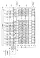
図2は、図1に示したスイッチング部及び電流ソース部を詳細に示す図である。
図2を参照すれば、本発明の電流ソース部180はチャネル毎に形成される電流源Isを備える。FIG. 2 is a diagram illustrating the switching unit and the current source unit illustrated in FIG. 1 in detail.
Referring to FIG. 2, the
電流源Isはセンシング期間にデータ線D1〜Dmに所定の電流を供給する。データ線D1〜Dmに供給された所定の電流は、制御信号によって選択されたサブ画素140に供給される。この場合、サブ画素140のそれぞれに含まれる有機発光ダイオードに所定の電流に対応する電圧が印加される。 The current source Is supplies a predetermined current to the data lines D1 to Dm during the sensing period. The predetermined current supplied to the data lines D1 to Dm is supplied to the sub-pixel 140 selected by the control signal. In this case, a voltage corresponding to a predetermined current is applied to the organic light emitting diodes included in each of the sub-pixels 140.
一方、図2では電流源Isがチャネル毎に設置されると示したが、本発明はこれに限定されるものではない。例えば、1つの電流源Isがあらゆる第4スイッチSW4と接続されてもよい。 On the other hand, FIG. 2 shows that the current source Is is installed for each channel, but the present invention is not limited to this. For example, one current source Is may be connected to every fourth switch SW4.
また、赤色サブ画素R、緑色サブ画素G及び青色サブ画素Bに電流を供給するための電流源が互いに異なるように設定されてもよい。詳細に説明すれば、赤色サブ画素R、緑色サブ画素G及び青色サブ画素Bのそれぞれに含まれる有機発光ダイオードは互いに異なる材料で形成される。従って、それぞれのサブ画素R、G、Bに含まれる有機発光ダイオードの特性を考慮して、互いに異なる電流を供給できるように赤色サブ画素R、緑色サブ画素G及び青色サブ画素Bに電流を供給するための電流源を互いに異なるように設定することもできる。 The current sources for supplying current to the red subpixel R, the green subpixel G, and the blue subpixel B may be set to be different from each other. More specifically, the organic light emitting diodes included in each of the red sub-pixel R, the green sub-pixel G, and the blue sub-pixel B are formed of different materials. Accordingly, in consideration of the characteristics of the organic light emitting diodes included in the sub-pixels R, G, and B, currents are supplied to the red sub-pixel R, the green sub-pixel G, and the blue sub-pixel B so that different currents can be supplied. It is also possible to set different current sources for the purpose.
スイッチング部170は、それぞれのチャネル毎に形成される第4スイッチSW4及び第5スイッチSW5と、第1〜第3スイッチSW1〜SW3を備える。ここで、第1スイッチSW1、第2スイッチSW2及び第3スイッチSW3は、それぞれ赤色サブ画素Rと接続されたデータ線D1、D4、...、緑色サブ画素Gと接続されたデータ線D2、D5、...及び青色サブ画素Bと接続されたデータ線D3、D6、...のそれぞれと連結されるように形成される。 The
第4スイッチSW4は、電流源Isとデータ線Dとの間に位置する。このような第4スイッチSW4はセンシング期間にターンオンされる。ここで、センシング期間はサブ画素140のそれぞれに含まれる有機発光ダイオードの劣化を測定する期間であり、設計者によって多様な時点に配置される。例えば、センシング期間は有機電界発光表示装置に電源が供給される時点に位置され得る。 The fourth switch SW4 is located between the current source Is and the data line D. The fourth switch SW4 is turned on during the sensing period. Here, the sensing period is a period in which the deterioration of the organic light emitting diode included in each of the sub-pixels 140 is measured, and is arranged at various times by the designer. For example, the sensing period may be located when power is supplied to the organic light emitting display device.
第5スイッチSW5は、データ駆動部120とデータ線Dとの間に位置する。このような第5スイッチSW5は駆動期間にターンオンされる。ここで、駆動期間はセンシング期間を除いたサブ画素140で所定の映像が表示される期間を意味する。 The fifth switch SW5 is located between the
第1スイッチSW1は、赤色サブ画素Rと接続されたデータ線D1、D4、...のそれぞれと、第1ADC192との間に形成される。このような第1スイッチSW1は、制御線CL1〜CLnのそれぞれに制御信号が供給される毎に順次ターンオンされる。 The first switch SW1 is connected to the data lines D1, D4,. . . And the
第2スイッチSW2は、緑色サブ画素Gと接続されたデータ線D2、D5、...のそれぞれと、第2ADC194との間に形成される。このような第2スイッチSW2は、制御線CL1〜CLnのそれぞれに制御信号が供給される毎に順次ターンオンされる。 The second switch SW2 is connected to the data lines D2, D5,. . . And the
第3スイッチSW3は、青色サブ画素Bと接続されたデータ線D3、D6、...のそれぞれと、第3ADC196との間に形成される。このような第3スイッチSW3は、制御線CL1〜CLnのそれぞれに制御信号が供給される毎に順次ターンオンされる。 The third switch SW3 is connected to the data lines D3, D6,. . . And the
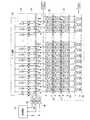
図3は、本発明の実施形態に係るサブ画素の実施形態を示す図である。図3では説明の便宜上、第mのデータ線Dm及び第nの走査線Snに接続された画素を示す。
図3を参照すれば、本発明の実施形態に係るサブ画素140は、有機発光ダイオードOLEDと、有機発光ダイオードOLEDに電流を供給するための画素回路142とを備える。FIG. 3 is a diagram illustrating an embodiment of a sub-pixel according to an embodiment of the present invention. FIG. 3 shows pixels connected to the mth data line Dm and the nth scanning line Sn for convenience of explanation.
Referring to FIG. 3, the sub-pixel 140 according to the embodiment of the present invention includes an organic light emitting diode OLED and a
有機発光ダイオードOLEDのアノード電極は画素回路142に接続され、カソード電極は第2電源ELVSSに接続される。このような有機発光ダイオードOLEDは、画素回路142から供給される電流に対応して所定輝度の光を生成する。 The anode electrode of the organic light emitting diode OLED is connected to the
画素回路142は走査線Snに走査信号が供給される時にデータ線Dmからデータ信号の供給を受ける。また、画素回路142は制御線CLnに制御信号が供給される時に電流ソース部180から所定の電流データの供給を受け、供給を受けた電流に対応する電圧を第3ADC196に供給する。このために、画素回路142は4つのトランジスタM1〜M4及びストレージキャパシタCstを備える。 The
第1トランジスタM1のゲート電極は走査線Snに接続され、第1電極はデータ線Dmに接続される。そして、第1トランジスタM1の第2電極はストレージキャパシタCstの第1端子に接続される。このような第1トランジスタM1は走査線Snに走査信号が供給される時にターンオンされる。ここで、走査信号はストレージキャパシタCstにデータ信号に対応する電圧が充電される期間に供給される。 The gate electrode of the first transistor M1 is connected to the scanning line Sn, and the first electrode is connected to the data line Dm. The second electrode of the first transistor M1 is connected to the first terminal of the storage capacitor Cst. The first transistor M1 is turned on when a scanning signal is supplied to the scanning line Sn. Here, the scanning signal is supplied during a period in which the storage capacitor Cst is charged with a voltage corresponding to the data signal.
第2トランジスタM2のゲート電極はストレージキャパシタCstの第1端子に接続され、第1電極はストレージキャパシタCstの第2端子及び第1電源ELVDDに接続される。このような第2トランジスタM2は、ストレージキャパシタCstに格納された電圧値に対応して第1電源ELVDDから有機発光ダイオードOLEDを経由して第2電源ELVSSに流れる電流量を制御する。このとき、有機発光ダイオードOLEDは、第2トランジスタM2から供給される電流量に対応する光を生成する。 The gate electrode of the second transistor M2 is connected to the first terminal of the storage capacitor Cst, and the first electrode is connected to the second terminal of the storage capacitor Cst and the first power supply ELVDD. The second transistor M2 controls the amount of current flowing from the first power supply ELVDD to the second power supply ELVSS via the organic light emitting diode OLED corresponding to the voltage value stored in the storage capacitor Cst. At this time, the organic light emitting diode OLED generates light corresponding to the amount of current supplied from the second transistor M2.
第3トランジスタM3のゲート電極は発光制御線Enに接続され、第1電極は第2トランジスタM2の第2電極に接続される。そして、第3トランジスタM3の第2電極は有機発光ダイオードOLEDに接続される。このような第3トランジスタM3は発光制御線Enに発光制御信号が供給される時にターンオフされ、発光制御信号が供給されない時にターンオンされる。ここで、発光制御信号はストレージキャパシタCstにデータ信号に対応する電圧が充電される期間及び有機発光ダイオードOLEDの劣化情報がセンシングされるセンシング期間に供給される。 The gate electrode of the third transistor M3 is connected to the light emission control line En, and the first electrode is connected to the second electrode of the second transistor M2. The second electrode of the third transistor M3 is connected to the organic light emitting diode OLED. The third transistor M3 is turned off when the light emission control signal is supplied to the light emission control line En, and turned on when the light emission control signal is not supplied. Here, the light emission control signal is supplied during a period during which the voltage corresponding to the data signal is charged in the storage capacitor Cst and during a sensing period during which deterioration information of the organic light emitting diode OLED is sensed.
第4トランジスタM4のゲート電極は制御線CLnに接続され、第1電極は第3トランジスタM3の第2電極に接続される。また、第4トランジスタM4の第2電極はデータ線Dmに接続される。このような第4トランジスタM4は、制御線CLnに制御信号が供給される時にターンオンされ、それ以外の場合にターンオフされる。ここで、制御線CL1〜CLnに供給される制御信号はセンシング期間に順次供給される。 The gate electrode of the fourth transistor M4 is connected to the control line CLn, and the first electrode is connected to the second electrode of the third transistor M3. The second electrode of the fourth transistor M4 is connected to the data line Dm. The fourth transistor M4 is turned on when a control signal is supplied to the control line CLn, and is turned off in other cases. Here, the control signals supplied to the control lines CL1 to CLn are sequentially supplied during the sensing period.
図4は、図2に示したスイッチング部の動作過程を示す波形図である。そして、図5A〜図5Eは、図4の波形図に対応するスイッチの動作過程を示す図である。
図4〜図5Eを参照して動作過程を詳細に説明すれば、まず、センシング期間に制御線CL1〜CLnに制御信号が順次供給される。そして、センシング期間に図5Aに示すように、第4スイッチSW4がターンオン状態を維持する。FIG. 4 is a waveform diagram illustrating an operation process of the switching unit illustrated in FIG. 5A to 5E are diagrams illustrating an operation process of the switch corresponding to the waveform diagram of FIG.
The operation process will be described in detail with reference to FIGS. 4 to 5E. First, control signals are sequentially supplied to the control lines CL1 to CLn in the sensing period. Then, as shown in FIG. 5A, the fourth switch SW4 maintains the turn-on state during the sensing period.
まず、第1制御線CL1に制御信号が供給されると、第1制御線CL1と接続されたサブ画素140に含まれる第4トランジスタM4がターンオンされる。すると、電流源Isの電流がデータ線D1〜Dm及び第4トランジスタM4を経由してサブ画素140の有機発光ダイオードOLEDに供給される。このとき、有機発光ダイオードOLEDには劣化に対応する所定の電圧が印加される。 First, when a control signal is supplied to the first control line CL1, the fourth transistor M4 included in the sub-pixel 140 connected to the first control line CL1 is turned on. Then, the current from the current source Is is supplied to the organic light emitting diode OLED of the sub-pixel 140 via the data lines D1 to Dm and the fourth transistor M4. At this time, a predetermined voltage corresponding to deterioration is applied to the organic light emitting diode OLED.
第1制御線CL1に制御信号が供給される期間に第1スイッチSW1、第2スイッチSW2及び第3スイッチSW3が画素単位で順次ターンオンされる。詳細に説明すれば、赤色サブ画素R、緑色サブ画素G及び青色サブ画素Bは1つの画素をなす。ここで、第1スイッチSW1、第2スイッチSW2及び第3スイッチSW3は画素単位でターンオンされながら、ADC192、194、196に有機発光ダイオードOLEDに印加された電圧を提供する。 The first switch SW1, the second switch SW2, and the third switch SW3 are sequentially turned on in units of pixels during a period in which a control signal is supplied to the first control line CL1. In detail, the red sub-pixel R, the green sub-pixel G, and the blue sub-pixel B form one pixel. Here, the first switch SW1, the second switch SW2, and the third switch SW3 provide the voltage applied to the organic light emitting diode OLED to the
実際に、第1スイッチSW1は、図5B〜図5Eに示すように、順次ターンオンされる。そして、第2スイッチSW2及び第3スイッチSW3も順次ターンオンされる。ここで、同一な画素をなすサブ画素140と接続されたスイッチSW1、SW2、SW3は同時にターンオンされながら、サブ画素140のそれぞれの有機発光ダイオードOLEDに印加された電圧をADC192、194、196に供給する。すると、ADC192、194、196は自分に供給される電圧をデジタル信号に変換して劣化補償部200に供給する。 Actually, the first switch SW1 is sequentially turned on as shown in FIGS. 5B to 5E. The second switch SW2 and the third switch SW3 are also turned on sequentially. Here, the switches SW1, SW2, and SW3 connected to the sub-pixel 140 forming the same pixel are simultaneously turned on, and the voltages applied to the respective organic light emitting diodes OLED of the sub-pixel 140 are supplied to the
その後、第1制御線CL1に制御信号の供給が中断されると同時に第2制御線CL2に制御信号が供給される。すると、第1乃至第3スイッチSW1〜SW3は、図5B〜5Eに示すように、順次ターンオンされながら第2制御線CL2と接続されたサブ画素140のそれぞれの有機発光ダイオードOLEDに印加された電圧をADC192、194、196に供給する。 Thereafter, the supply of the control signal to the first control line CL1 is interrupted, and at the same time, the control signal is supplied to the second control line CL2. Then, as shown in FIGS. 5B to 5E, the first to third switches SW1 to SW3 are sequentially turned on and voltages applied to the respective organic light emitting diodes OLED of the sub-pixels 140 connected to the second control line CL2. Is supplied to the
実際に、本発明ではセンシング期間に第1制御線CL1〜第nの制御線CLnに制御信号が順次供給される。すると、制御信号が供給される期間毎にスイッチSW1〜SW3が画素単位で順次ターンオンされながら、サブ画素140の劣化に対応する電圧をADC192、194、196に供給する。 Actually, in the present invention, control signals are sequentially supplied to the first control line CL1 to the nth control line CLn in the sensing period. Then, the switches SW <b> 1 to SW <b> 3 are sequentially turned on in units of pixels every period during which the control signal is supplied, and a voltage corresponding to the deterioration of the sub-pixel 140 is supplied to the
その後、劣化補償部200はADC192、194、196から供給されるデジタル信号(劣化情報)を用いてタイミング制御部150を制御する。すると、タイミング制御部150は劣化が補償され得るように、第1データData1のビット値を変更して第2データData2を生成し、生成された第2データData2をデータ駆動部120に供給する。データ駆動部120は、駆動期間に第2データData2を用いてデータ信号を生成し、生成されたデータ信号をデータ線D1〜Dmに供給する。そのために、駆動期間には第5スイッチSW5がターンオンされる。 Thereafter, the
前述したように、本発明では3つのADC192、194、196を共有しながらサブ画素140の劣化情報を劣化補償部200に提供できる。一方、本発明において、ADC192、194、196の数は少なくても1つ以上に設定されることができる(データ線の数よりは少ない数に設定)。例えば、1つのADCが設置される場合、第1スイッチSW1、第2スイッチSW2及び第3スイッチSW3が1つずつ順次ターンオンされながら(サブ画素単位でターンオン)、サブ画素140の劣化情報をADCに提供する。 As described above, in the present invention, the degradation information of the sub-pixel 140 can be provided to the
以上説明したように、本発明の最も好ましい実施の形態等について説明したが、本発明は、上記記載に限定されるものではなく、特許請求の範囲に記載され、または明細書に開示された発明の要旨に基づき、当業者において様々な変形や変更が可能であることは勿論であり、斯かる変形や変更が、本発明の範囲に含まれることは言うまでもない。 As described above, the most preferred embodiment of the present invention has been described. However, the present invention is not limited to the above description, and is described in the claims or disclosed in the specification. It goes without saying that various modifications and changes can be made by those skilled in the art based on the above gist, and such modifications and changes are included in the scope of the present invention.
110 走査駆動部
120 データ駆動部
150 タイミング制御部
160 制御線駆動部
170 スイッチング部
180 電流ソース部
200 劣化補償部110 Scan driver
120
Claims (12)
Translated fromJapanese前記サブ画素のそれぞれに含まれる有機発光ダイオードの劣化情報を把握するためのセンシング期間に所定電流を前記有機発光ダイオードに供給するための電流ソース部と、
前記有機発光ダイオードに印加された電圧をデジタル信号に変換するために前記データ線の数よりも少ない数で形成される少なくとも1つ以上のアナログ-デジタル変換部と、
前記センシング期間に前記データ線と前記電流ソース部とを接続させ、前記センシング期間に前記少なくとも1つ以上のアナログ-デジタル変換部を前記データ線と順次接続させるためのスイッチング部と
を備えることを特徴とする有機電界発光表示装置。A sub-pixel located at the intersection of the scan line and the data line;
A current source unit for supplying a predetermined current to the organic light emitting diode during a sensing period for grasping deterioration information of the organic light emitting diode included in each of the sub-pixels;
At least one analog-to-digital converter formed with a number smaller than the number of the data lines in order to convert a voltage applied to the organic light emitting diode into a digital signal;
A switching unit for connecting the data line and the current source unit during the sensing period, and sequentially connecting the at least one analog-digital conversion unit with the data line during the sensing period. An organic electroluminescent display device.
赤色サブ画素に含まれる有機発光ダイオードの電圧をデジタル信号に変換するための第1アナログ-デジタル変換部と、
緑色サブ画素に含まれる有機発光ダイオードの電圧をデジタル信号に変換するための第2アナログ-デジタル変換部と、
青色サブ画素に含まれる有機発光ダイオードの電圧をデジタル信号に変換するための第3アナログ-デジタル変換部と
を備えることを特徴とする請求項1に記載の有機電界発光表示装置。The at least one analog-to-digital conversion unit includes:
A first analog-digital converter for converting the voltage of the organic light emitting diode included in the red sub-pixel into a digital signal;
A second analog-digital converter for converting the voltage of the organic light emitting diode included in the green sub-pixel into a digital signal;
The organic light emitting display as claimed in claim 1, further comprising a third analog-digital converter for converting a voltage of the organic light emitting diode included in the blue sub-pixel into a digital signal.
前記劣化補償部の制御によって前記劣化が補償され得るようにデータのビット値を変更するためのタイミング制御部と、
前記タイミング制御部から供給されるデータをデータ信号に変換して前記データ線に供給するためのデータ駆動部と、
前記走査線に走査信号を供給し、前記走査線と平行に形成される制御線に制御信号を供給する走査駆動部と
を更に備えることを特徴とする請求項2に記載の有機電界発光表示装置。A deterioration compensator for controlling the organic light emitting diode to be compensated for deterioration corresponding to a digital signal supplied from the first to third analog-digital converters;
A timing control unit for changing a bit value of data so that the degradation can be compensated by the control of the degradation compensation unit;
A data driver for converting data supplied from the timing controller into a data signal and supplying the data signal;
The organic light emitting display according to claim 2, further comprising: a scan driver that supplies a scan signal to the scan line and supplies a control signal to a control line formed in parallel with the scan line. .
前記データ駆動部とデータ線との間に形成される第5スイッチと、
前記赤色サブ画素と接続されたデータ線のそれぞれと前記第1アナログ-デジタル変換部との間に位置する第1スイッチと、
前記緑色サブ画素と接続されたデータ線のそれぞれと前記第2アナログ-デジタル変換部との間に位置する第2スイッチと、
前記青色サブ画素と接続されたデータ線のそれぞれと前記第3アナログ-デジタル変換部との間に位置する第3スイッチと
を備えることを特徴とする請求項4に記載の有機電界発光表示装置。A fourth switch formed between the current source unit and the data line;
A fifth switch formed between the data driver and the data line;
A first switch located between each of the data lines connected to the red sub-pixel and the first analog-digital converter;
A second switch located between each of the data lines connected to the green sub-pixel and the second analog-digital converter;
5. The organic light emitting display as claimed in claim 4, further comprising a third switch positioned between each of the data lines connected to the blue sub-pixel and the third analog-digital converter.
前記所定の電流に対応して前記有機発光ダイオードに印加される電圧を少なくとも1つ以上のアナログ-デジタル変換部を共有しながら、デジタル信号に変換する段階と、
前記デジタル信号に対応して前記有機発光ダイオードの劣化が補償され得るようにデータのビット値を変更する段階と、
駆動期間に前記データを用いてデータ信号を生成し、前記データ信号を前記サブ画素に供給する段階と
を含むことを特徴とする有機電界発光表示装置の駆動方法。Supplying a predetermined current to the organic light emitting diodes included in each of the sub-pixels in units of horizontal lines during the sensing period;
Converting a voltage applied to the organic light emitting diode corresponding to the predetermined current into a digital signal while sharing at least one analog-digital conversion unit;
Changing a bit value of data so that deterioration of the organic light emitting diode can be compensated for in response to the digital signal;
Generating a data signal using the data during a driving period, and supplying the data signal to the sub-pixel.
第1アナログ-デジタル変換部を赤色サブ画素と、第2アナログ-デジタル変換部を緑色サブ画素と、第3アナログ-デジタル変換部を青色サブ画素と順次接続させながら、前記デジタル信号を生成することを特徴とする請求項10に記載の有機電界発光表示装置の駆動方法。Converting to the digital signal comprises:
Generating the digital signal while sequentially connecting the first analog-digital converter to the red sub-pixel, the second analog-digital converter to the green sub-pixel, and the third analog-digital converter to the blue sub-pixel. The method of driving an organic light emitting display according to claim 10.
Applications Claiming Priority (2)
| Application Number | Priority Date | Filing Date | Title |
|---|---|---|---|
| KR10-2008-0006143 | 2008-01-21 | ||
| KR1020080006143AKR100969769B1 (en) | 2008-01-21 | 2008-01-21 | Organic light emitting display device and driving method thereof |
Publications (2)
| Publication Number | Publication Date |
|---|---|
| JP2009175652Atrue JP2009175652A (en) | 2009-08-06 |
| JP4980977B2 JP4980977B2 (en) | 2012-07-18 |
Family
ID=40568425
Family Applications (1)
| Application Number | Title | Priority Date | Filing Date |
|---|---|---|---|
| JP2008105891AActiveJP4980977B2 (en) | 2008-01-21 | 2008-04-15 | Organic electroluminescent display device and driving method thereof |
Country Status (5)
| Country | Link |
|---|---|
| US (1) | US20090184896A1 (en) |
| EP (1) | EP2081177A3 (en) |
| JP (1) | JP4980977B2 (en) |
| KR (1) | KR100969769B1 (en) |
| CN (1) | CN101494023B (en) |
Cited By (1)
| Publication number | Priority date | Publication date | Assignee | Title |
|---|---|---|---|---|
| JP2011095750A (en)* | 2009-10-30 | 2011-05-12 | Silicon Works Co Ltd | Circuit and method for driving organic light-emitting diode (oled) display |
Families Citing this family (24)
| Publication number | Priority date | Publication date | Assignee | Title |
|---|---|---|---|---|
| KR101056317B1 (en)* | 2009-04-02 | 2011-08-11 | 삼성모바일디스플레이주식회사 | Pixel and organic light emitting display device using same |
| KR101178910B1 (en) | 2009-07-30 | 2012-09-03 | 삼성디스플레이 주식회사 | Organic Light Emitting Display Device and Driving Voltage Setting Method Thereof |
| KR101056281B1 (en) | 2009-08-03 | 2011-08-11 | 삼성모바일디스플레이주식회사 | Organic electroluminescent display and driving method thereof |
| KR20110013693A (en)* | 2009-08-03 | 2011-02-10 | 삼성모바일디스플레이주식회사 | Organic electroluminescent display and driving method thereof |
| KR101101097B1 (en)* | 2009-11-04 | 2012-01-03 | 삼성모바일디스플레이주식회사 | Organic light emitting display device and driving method thereof |
| KR101073226B1 (en)* | 2010-03-17 | 2011-10-12 | 삼성모바일디스플레이주식회사 | Organic Light Emitting Display Device |
| KR101223488B1 (en)* | 2010-05-11 | 2013-01-17 | 삼성디스플레이 주식회사 | Organic Light Emitting Display and Driving Method Thereof |
| KR101155897B1 (en)* | 2010-05-11 | 2012-06-20 | 삼성모바일디스플레이주식회사 | Display device |
| CN101861021A (en)* | 2010-05-25 | 2010-10-13 | 北京大学深圳研究生院 | A LED digital power supply drive management control circuit for lighting |
| KR101645404B1 (en)* | 2010-07-06 | 2016-08-04 | 삼성디스플레이 주식회사 | Organic Light Emitting Display |
| KR101147426B1 (en)* | 2010-10-27 | 2012-05-23 | 삼성모바일디스플레이주식회사 | Stereopsis display device and driving method thereof |
| KR101470688B1 (en)* | 2011-12-08 | 2014-12-08 | 엘지디스플레이 주식회사 | Organic Light Emitting Display And Compensation Method Of Degradation Thereof |
| KR101350592B1 (en)* | 2011-12-12 | 2014-01-16 | 엘지디스플레이 주식회사 | Organic light-emitting display device |
| KR101362002B1 (en)* | 2011-12-12 | 2014-02-11 | 엘지디스플레이 주식회사 | Organic light-emitting display device |
| KR101993747B1 (en)* | 2013-04-02 | 2019-07-02 | 삼성디스플레이 주식회사 | Organic Light Emitting Display Device and Driving Method Thereof |
| KR102238468B1 (en)* | 2013-12-16 | 2021-04-09 | 엘지디스플레이 주식회사 | Organic light emitting diode display device |
| CN104392685B (en)* | 2014-12-15 | 2017-06-09 | 合肥京东方光电科技有限公司 | Array base palte, display panel and polarity reversal driving method |
| KR102332276B1 (en)* | 2015-01-26 | 2021-12-01 | 엘지디스플레이 주식회사 | Organic Light Emitting Display For Sensing Degradation Of Organic Light Emitting Diode |
| CN105243996B (en)* | 2015-11-09 | 2018-01-30 | 深圳市华星光电技术有限公司 | Using the AMOLED drive circuit structures of external compensation |
| KR102509604B1 (en)* | 2015-12-30 | 2023-03-14 | 삼성디스플레이 주식회사 | Display apparatus |
| TWI683297B (en)* | 2017-11-21 | 2020-01-21 | 聯詠科技股份有限公司 | Driving apparatus for driving display panel |
| US10643543B2 (en)* | 2017-11-23 | 2020-05-05 | Novatek Microelectronics Corp. | Multi-sensing channels design for pixel compensation |
| US20220093035A1 (en)* | 2020-09-22 | 2022-03-24 | Innolux Corporation | Pixel circuit for a display device which has a compensation circuit for color shift issue |
| CN114333707A (en)* | 2020-09-29 | 2022-04-12 | 中强光电股份有限公司 | Driving device and driving method of backlight module |
Citations (6)
| Publication number | Priority date | Publication date | Assignee | Title |
|---|---|---|---|---|
| JP2002229513A (en)* | 2001-02-06 | 2002-08-16 | Tohoku Pioneer Corp | Device for driving organic el display panel |
| JP2005055909A (en)* | 2003-08-07 | 2005-03-03 | Barco Nv | OLED display element, control device for controlling it, and method for optimizing its service life |
| JP2008102404A (en)* | 2006-10-20 | 2008-05-01 | Hitachi Displays Ltd | Display device |
| JP2008224863A (en)* | 2007-03-09 | 2008-09-25 | Hitachi Displays Ltd | Image display device |
| JP2009075178A (en)* | 2007-09-19 | 2009-04-09 | Hitachi Displays Ltd | Image display device |
| JP2009168927A (en)* | 2008-01-11 | 2009-07-30 | Hitachi Displays Ltd | Organic EL display device |
Family Cites Families (16)
| Publication number | Priority date | Publication date | Assignee | Title |
|---|---|---|---|---|
| JP3866606B2 (en) | 2002-04-08 | 2007-01-10 | Necエレクトロニクス株式会社 | Display device drive circuit and drive method thereof |
| JP2005128089A (en)* | 2003-10-21 | 2005-05-19 | Tohoku Pioneer Corp | Luminescent display device |
| US8421715B2 (en)* | 2004-05-21 | 2013-04-16 | Semiconductor Energy Laboratory Co., Ltd. | Display device, driving method thereof and electronic appliance |
| CA2472671A1 (en)* | 2004-06-29 | 2005-12-29 | Ignis Innovation Inc. | Voltage-programming scheme for current-driven amoled displays |
| KR100624310B1 (en)* | 2004-08-20 | 2006-09-19 | 삼성에스디아이 주식회사 | Light emitting display device and brightness control method |
| KR100748739B1 (en)* | 2005-01-28 | 2007-08-13 | 도시바 마쯔시따 디스플레이 테크놀로지 컴퍼니, 리미티드 | El display apparatus and method of driving the same |
| JP5020484B2 (en)* | 2005-07-12 | 2012-09-05 | 東北パイオニア株式会社 | Self-luminous display device and driving method thereof |
| JP2007064999A (en)* | 2005-08-29 | 2007-03-15 | Mitsubishi Electric Corp | Liquid crystal display |
| TWI450247B (en)* | 2006-02-10 | 2014-08-21 | Ignis Innovation Inc | Method and system for pixel circuit displays |
| KR101200884B1 (en)* | 2006-06-14 | 2012-11-13 | 엘지디스플레이 주식회사 | Light Emitting Diode and Light Emitting Display Device and Method for Driving the same |
| EP1879171A1 (en)* | 2006-07-10 | 2008-01-16 | THOMSON Licensing | Organic electroluminescent display |
| GB2441354B (en)* | 2006-08-31 | 2009-07-29 | Cambridge Display Tech Ltd | Display drive systems |
| KR100858615B1 (en) | 2007-03-22 | 2008-09-17 | 삼성에스디아이 주식회사 | Organic light emitting display device and driving method thereof |
| KR100846970B1 (en) | 2007-04-10 | 2008-07-17 | 삼성에스디아이 주식회사 | Organic light emitting display device and driving method thereof |
| KR100858616B1 (en) | 2007-04-10 | 2008-09-17 | 삼성에스디아이 주식회사 | Organic light emitting display device and driving method thereof |
| US7859501B2 (en)* | 2007-06-22 | 2010-12-28 | Global Oled Technology Llc | OLED display with aging and efficiency compensation |
- 2008
- 2008-01-21KRKR1020080006143Apatent/KR100969769B1/enactiveActive
- 2008-04-15JPJP2008105891Apatent/JP4980977B2/enactiveActive
- 2008-07-08USUS12/169,089patent/US20090184896A1/ennot_activeAbandoned
- 2009
- 2009-01-20EPEP09150959Apatent/EP2081177A3/ennot_activeWithdrawn
- 2009-01-21CNCN2009100032482Apatent/CN101494023B/enactiveActive
Patent Citations (6)
| Publication number | Priority date | Publication date | Assignee | Title |
|---|---|---|---|---|
| JP2002229513A (en)* | 2001-02-06 | 2002-08-16 | Tohoku Pioneer Corp | Device for driving organic el display panel |
| JP2005055909A (en)* | 2003-08-07 | 2005-03-03 | Barco Nv | OLED display element, control device for controlling it, and method for optimizing its service life |
| JP2008102404A (en)* | 2006-10-20 | 2008-05-01 | Hitachi Displays Ltd | Display device |
| JP2008224863A (en)* | 2007-03-09 | 2008-09-25 | Hitachi Displays Ltd | Image display device |
| JP2009075178A (en)* | 2007-09-19 | 2009-04-09 | Hitachi Displays Ltd | Image display device |
| JP2009168927A (en)* | 2008-01-11 | 2009-07-30 | Hitachi Displays Ltd | Organic EL display device |
Cited By (2)
| Publication number | Priority date | Publication date | Assignee | Title |
|---|---|---|---|---|
| JP2011095750A (en)* | 2009-10-30 | 2011-05-12 | Silicon Works Co Ltd | Circuit and method for driving organic light-emitting diode (oled) display |
| US9311858B2 (en) | 2009-10-30 | 2016-04-12 | Silicon Works Co., Ltd. | Circuit and method for driving OLED display |
Also Published As
| Publication number | Publication date |
|---|---|
| EP2081177A3 (en) | 2009-12-16 |
| JP4980977B2 (en) | 2012-07-18 |
| KR20090080270A (en) | 2009-07-24 |
| US20090184896A1 (en) | 2009-07-23 |
| KR100969769B1 (en) | 2010-07-13 |
| EP2081177A2 (en) | 2009-07-22 |
| CN101494023B (en) | 2011-12-14 |
| CN101494023A (en) | 2009-07-29 |
Similar Documents
| Publication | Publication Date | Title |
|---|---|---|
| JP4980977B2 (en) | Organic electroluminescent display device and driving method thereof | |
| CN103971631B (en) | Organic light emitting display device and driving method thereof | |
| US9595228B2 (en) | Pixel array and organic light emitting display device including the same | |
| US8405582B2 (en) | Organic light emitting display and driving method thereof | |
| EP2237254B1 (en) | Pixel and organic light emitting display device using the same | |
| KR102050268B1 (en) | Organic light emitting display device | |
| JP4981098B2 (en) | Pixel and organic light emitting display using the same | |
| US8284132B2 (en) | Organic light emitting display device and method of driving the same | |
| JP5080765B2 (en) | Data driving circuit, flat panel display device including the same, and data driving method thereof | |
| US8558766B2 (en) | Organic light emitting display and method of driving the same | |
| US20110084955A1 (en) | Organic light emitting display | |
| KR101034690B1 (en) | Organic light emitting display device and driving method thereof | |
| KR101676780B1 (en) | Pixel and Organic Light Emitting Display Using the same | |
| KR102415732B1 (en) | Subpixel Circuit, Organic Light Emitting Display Device and Method of Driving the same | |
| KR20090080269A (en) | Organic light emitting display device and driving method thereof | |
| KR20240100697A (en) | Driving Device And Driving Method Of Electroluminescence Display Apparatus | |
| KR20150100997A (en) | Organic light emitting display device | |
| KR102656041B1 (en) | Display device and method for controlling display device |
Legal Events
| Date | Code | Title | Description |
|---|---|---|---|
| A131 | Notification of reasons for refusal | Free format text:JAPANESE INTERMEDIATE CODE: A131 Effective date:20110405 | |
| A521 | Request for written amendment filed | Free format text:JAPANESE INTERMEDIATE CODE: A523 Effective date:20110704 | |
| RD02 | Notification of acceptance of power of attorney | Free format text:JAPANESE INTERMEDIATE CODE: A7422 Effective date:20110704 | |
| A131 | Notification of reasons for refusal | Free format text:JAPANESE INTERMEDIATE CODE: A131 Effective date:20111213 | |
| A521 | Request for written amendment filed | Free format text:JAPANESE INTERMEDIATE CODE: A523 Effective date:20120301 | |
| TRDD | Decision of grant or rejection written | ||
| A01 | Written decision to grant a patent or to grant a registration (utility model) | Free format text:JAPANESE INTERMEDIATE CODE: A01 Effective date:20120327 | |
| A01 | Written decision to grant a patent or to grant a registration (utility model) | Free format text:JAPANESE INTERMEDIATE CODE: A01 | |
| A61 | First payment of annual fees (during grant procedure) | Free format text:JAPANESE INTERMEDIATE CODE: A61 Effective date:20120419 | |
| FPAY | Renewal fee payment (event date is renewal date of database) | Free format text:PAYMENT UNTIL: 20150427 Year of fee payment:3 | |
| R150 | Certificate of patent or registration of utility model | Ref document number:4980977 Country of ref document:JP Free format text:JAPANESE INTERMEDIATE CODE: R150 Free format text:JAPANESE INTERMEDIATE CODE: R150 | |
| FPAY | Renewal fee payment (event date is renewal date of database) | Free format text:PAYMENT UNTIL: 20150427 Year of fee payment:3 | |
| S111 | Request for change of ownership or part of ownership | Free format text:JAPANESE INTERMEDIATE CODE: R313115 | |
| FPAY | Renewal fee payment (event date is renewal date of database) | Free format text:PAYMENT UNTIL: 20150427 Year of fee payment:3 | |
| R350 | Written notification of registration of transfer | Free format text:JAPANESE INTERMEDIATE CODE: R350 | |
| R250 | Receipt of annual fees | Free format text:JAPANESE INTERMEDIATE CODE: R250 | |
| R250 | Receipt of annual fees | Free format text:JAPANESE INTERMEDIATE CODE: R250 | |
| R250 | Receipt of annual fees | Free format text:JAPANESE INTERMEDIATE CODE: R250 | |
| R250 | Receipt of annual fees | Free format text:JAPANESE INTERMEDIATE CODE: R250 | |
| R250 | Receipt of annual fees | Free format text:JAPANESE INTERMEDIATE CODE: R250 | |
| R250 | Receipt of annual fees | Free format text:JAPANESE INTERMEDIATE CODE: R250 | |
| R250 | Receipt of annual fees | Free format text:JAPANESE INTERMEDIATE CODE: R250 | |
| R250 | Receipt of annual fees | Free format text:JAPANESE INTERMEDIATE CODE: R250 | |
| R250 | Receipt of annual fees | Free format text:JAPANESE INTERMEDIATE CODE: R250 | |
| R250 | Receipt of annual fees | Free format text:JAPANESE INTERMEDIATE CODE: R250 | |
| R250 | Receipt of annual fees | Free format text:JAPANESE INTERMEDIATE CODE: R250 |