JP2009168867A - Display device - Google Patents
Display deviceDownload PDFInfo
- Publication number
- JP2009168867A JP2009168867AJP2008003849AJP2008003849AJP2009168867AJP 2009168867 AJP2009168867 AJP 2009168867AJP 2008003849 AJP2008003849 AJP 2008003849AJP 2008003849 AJP2008003849 AJP 2008003849AJP 2009168867 AJP2009168867 AJP 2009168867A
- Authority
- JP
- Japan
- Prior art keywords
- terminal group
- reference voltage
- input terminal
- circuit
- gradation reference
- Prior art date
- Legal status (The legal status is an assumption and is not a legal conclusion. Google has not performed a legal analysis and makes no representation as to the accuracy of the status listed.)
- Pending
Links
Images


Classifications
- G—PHYSICS
- G09—EDUCATION; CRYPTOGRAPHY; DISPLAY; ADVERTISING; SEALS
- G09G—ARRANGEMENTS OR CIRCUITS FOR CONTROL OF INDICATING DEVICES USING STATIC MEANS TO PRESENT VARIABLE INFORMATION
- G09G3/00—Control arrangements or circuits, of interest only in connection with visual indicators other than cathode-ray tubes
- G09G3/20—Control arrangements or circuits, of interest only in connection with visual indicators other than cathode-ray tubes for presentation of an assembly of a number of characters, e.g. a page, by composing the assembly by combination of individual elements arranged in a matrix no fixed position being assigned to or needed to be assigned to the individual characters or partial characters
- G09G3/34—Control arrangements or circuits, of interest only in connection with visual indicators other than cathode-ray tubes for presentation of an assembly of a number of characters, e.g. a page, by composing the assembly by combination of individual elements arranged in a matrix no fixed position being assigned to or needed to be assigned to the individual characters or partial characters by control of light from an independent source
- G09G3/36—Control arrangements or circuits, of interest only in connection with visual indicators other than cathode-ray tubes for presentation of an assembly of a number of characters, e.g. a page, by composing the assembly by combination of individual elements arranged in a matrix no fixed position being assigned to or needed to be assigned to the individual characters or partial characters by control of light from an independent source using liquid crystals
- G09G3/3611—Control of matrices with row and column drivers
- G09G3/3696—Generation of voltages supplied to electrode drivers
- G—PHYSICS
- G09—EDUCATION; CRYPTOGRAPHY; DISPLAY; ADVERTISING; SEALS
- G09G—ARRANGEMENTS OR CIRCUITS FOR CONTROL OF INDICATING DEVICES USING STATIC MEANS TO PRESENT VARIABLE INFORMATION
- G09G3/00—Control arrangements or circuits, of interest only in connection with visual indicators other than cathode-ray tubes
- G09G3/20—Control arrangements or circuits, of interest only in connection with visual indicators other than cathode-ray tubes for presentation of an assembly of a number of characters, e.g. a page, by composing the assembly by combination of individual elements arranged in a matrix no fixed position being assigned to or needed to be assigned to the individual characters or partial characters
- G09G3/34—Control arrangements or circuits, of interest only in connection with visual indicators other than cathode-ray tubes for presentation of an assembly of a number of characters, e.g. a page, by composing the assembly by combination of individual elements arranged in a matrix no fixed position being assigned to or needed to be assigned to the individual characters or partial characters by control of light from an independent source
- G09G3/36—Control arrangements or circuits, of interest only in connection with visual indicators other than cathode-ray tubes for presentation of an assembly of a number of characters, e.g. a page, by composing the assembly by combination of individual elements arranged in a matrix no fixed position being assigned to or needed to be assigned to the individual characters or partial characters by control of light from an independent source using liquid crystals
- G09G3/3611—Control of matrices with row and column drivers
- G09G3/3648—Control of matrices with row and column drivers using an active matrix
- G—PHYSICS
- G09—EDUCATION; CRYPTOGRAPHY; DISPLAY; ADVERTISING; SEALS
- G09G—ARRANGEMENTS OR CIRCUITS FOR CONTROL OF INDICATING DEVICES USING STATIC MEANS TO PRESENT VARIABLE INFORMATION
- G09G3/00—Control arrangements or circuits, of interest only in connection with visual indicators other than cathode-ray tubes
- G09G3/20—Control arrangements or circuits, of interest only in connection with visual indicators other than cathode-ray tubes for presentation of an assembly of a number of characters, e.g. a page, by composing the assembly by combination of individual elements arranged in a matrix no fixed position being assigned to or needed to be assigned to the individual characters or partial characters
- G09G3/34—Control arrangements or circuits, of interest only in connection with visual indicators other than cathode-ray tubes for presentation of an assembly of a number of characters, e.g. a page, by composing the assembly by combination of individual elements arranged in a matrix no fixed position being assigned to or needed to be assigned to the individual characters or partial characters by control of light from an independent source
- G09G3/36—Control arrangements or circuits, of interest only in connection with visual indicators other than cathode-ray tubes for presentation of an assembly of a number of characters, e.g. a page, by composing the assembly by combination of individual elements arranged in a matrix no fixed position being assigned to or needed to be assigned to the individual characters or partial characters by control of light from an independent source using liquid crystals
- G09G3/3611—Control of matrices with row and column drivers
- G09G3/3674—Details of drivers for scan electrodes
- G09G3/3677—Details of drivers for scan electrodes suitable for active matrices only
- G—PHYSICS
- G09—EDUCATION; CRYPTOGRAPHY; DISPLAY; ADVERTISING; SEALS
- G09G—ARRANGEMENTS OR CIRCUITS FOR CONTROL OF INDICATING DEVICES USING STATIC MEANS TO PRESENT VARIABLE INFORMATION
- G09G3/00—Control arrangements or circuits, of interest only in connection with visual indicators other than cathode-ray tubes
- G09G3/20—Control arrangements or circuits, of interest only in connection with visual indicators other than cathode-ray tubes for presentation of an assembly of a number of characters, e.g. a page, by composing the assembly by combination of individual elements arranged in a matrix no fixed position being assigned to or needed to be assigned to the individual characters or partial characters
- G09G3/34—Control arrangements or circuits, of interest only in connection with visual indicators other than cathode-ray tubes for presentation of an assembly of a number of characters, e.g. a page, by composing the assembly by combination of individual elements arranged in a matrix no fixed position being assigned to or needed to be assigned to the individual characters or partial characters by control of light from an independent source
- G09G3/36—Control arrangements or circuits, of interest only in connection with visual indicators other than cathode-ray tubes for presentation of an assembly of a number of characters, e.g. a page, by composing the assembly by combination of individual elements arranged in a matrix no fixed position being assigned to or needed to be assigned to the individual characters or partial characters by control of light from an independent source using liquid crystals
- G09G3/3611—Control of matrices with row and column drivers
- G09G3/3685—Details of drivers for data electrodes
- G09G3/3688—Details of drivers for data electrodes suitable for active matrices only
- G—PHYSICS
- G09—EDUCATION; CRYPTOGRAPHY; DISPLAY; ADVERTISING; SEALS
- G09G—ARRANGEMENTS OR CIRCUITS FOR CONTROL OF INDICATING DEVICES USING STATIC MEANS TO PRESENT VARIABLE INFORMATION
- G09G2300/00—Aspects of the constitution of display devices
- G09G2300/08—Active matrix structure, i.e. with use of active elements, inclusive of non-linear two terminal elements, in the pixels together with light emitting or modulating elements
- G09G2300/0809—Several active elements per pixel in active matrix panels
- G09G2300/0842—Several active elements per pixel in active matrix panels forming a memory circuit, e.g. a dynamic memory with one capacitor
- G—PHYSICS
- G09—EDUCATION; CRYPTOGRAPHY; DISPLAY; ADVERTISING; SEALS
- G09G—ARRANGEMENTS OR CIRCUITS FOR CONTROL OF INDICATING DEVICES USING STATIC MEANS TO PRESENT VARIABLE INFORMATION
- G09G2310/00—Command of the display device
- G09G2310/02—Addressing, scanning or driving the display screen or processing steps related thereto
- G09G2310/0264—Details of driving circuits
- G09G2310/0278—Details of driving circuits arranged to drive both scan and data electrodes
- G—PHYSICS
- G09—EDUCATION; CRYPTOGRAPHY; DISPLAY; ADVERTISING; SEALS
- G09G—ARRANGEMENTS OR CIRCUITS FOR CONTROL OF INDICATING DEVICES USING STATIC MEANS TO PRESENT VARIABLE INFORMATION
- G09G2320/00—Control of display operating conditions
- G09G2320/02—Improving the quality of display appearance
- G09G2320/0223—Compensation for problems related to R-C delay and attenuation in electrodes of matrix panels, e.g. in gate electrodes or on-substrate video signal electrodes
Landscapes
- Engineering & Computer Science (AREA)
- Chemical & Material Sciences (AREA)
- Crystallography & Structural Chemistry (AREA)
- Physics & Mathematics (AREA)
- Computer Hardware Design (AREA)
- General Physics & Mathematics (AREA)
- Theoretical Computer Science (AREA)
- Control Of Indicators Other Than Cathode Ray Tubes (AREA)
- Devices For Indicating Variable Information By Combining Individual Elements (AREA)
- Liquid Crystal (AREA)
- Liquid Crystal Display Device Control (AREA)
Abstract
Translated fromJapaneseDescription
Translated fromJapanese本発明は、表示装置に係り、特に、駆動回路間でデジタル信号を転送する方式の表示装置に適用して有効な技術に関する。 The present invention relates to a display device, and more particularly to a technique that is effective when applied to a display device that transfers digital signals between drive circuits.
アクティブ素子として薄膜トランジスタを使用するTFT(Thin Film Transistor)方式の液晶表示モジュールは、パーソナルコンピュータ等の表示装置として広く使用されている。これらの液晶表示装置は、液晶表示パネルと、液晶表示パネルを駆動する駆動回路を備えている。
そして、このような液晶表示モジュールにおいて、例えば、下記特許文献1に記載されているように、カスケード接続された駆動回路(ドレインドライバ、あるいゲートドライバ)の先頭の駆動回路にのみ、デジタル信号(例えば、表示データ、あるいはクロック)を入力し、他の駆動回路には、駆動回路内を通して、デジタル信号を順次転送する方式(以下、デジタル信号順次転送方式と称する。)のものが知られている。
下記特許文献1に記載されている液晶表示装置では、駆動回路(ドレインドライバ、又はゲートドライバ)を構成する半導体チップ(IC)は、液晶表示パネルを構成する基板(例えば、ガラス基板)上に直接実装されている。また、各ドレインドライバの電源電圧は、液晶表示パネルに接続されたフレキシブル配線基板を介して電源回路から供給される。A TFT (Thin Film Transistor) type liquid crystal display module using a thin film transistor as an active element is widely used as a display device for a personal computer or the like. These liquid crystal display devices include a liquid crystal display panel and a drive circuit that drives the liquid crystal display panel.
In such a liquid crystal display module, for example, as described in Patent Document 1 below, a digital signal (only in the first drive circuit of a cascade-connected drive circuit (drain driver or gate driver) ( For example, a system in which display data or a clock) is input and a digital signal is sequentially transferred to the other drive circuit through the drive circuit (hereinafter referred to as a digital signal sequential transfer system) is known. .
In the liquid crystal display device described in Patent Document 1 below, a semiconductor chip (IC) constituting a drive circuit (drain driver or gate driver) is directly on a substrate (for example, a glass substrate) constituting a liquid crystal display panel. Has been implemented. Further, the power supply voltage of each drain driver is supplied from the power supply circuit via a flexible wiring board connected to the liquid crystal display panel.
なお、本願発明に関連する先行技術文献としては以下のものがある。
前述の特許文献1に記載されている液晶表示装置では、表示制御回路(タイミングコントローラ)は、液晶表示パネルを構成する基板上に実装されていない。しかしながら、表示制御回路(タイミングコントローラ)も、液晶表示パネルを構成する基板上に実装することが想定される。
そして、表示制御回路(タイミングコントローラ)を液晶表示パネルを構成する基板上に実装し、電源電圧および階調基準電圧を、液晶表示パネルを構成する基板外から供給する場合、表示制御回路(タイミングコントローラ)からドレインドライバへ供給する信号(表示データ、制御信号)の配線と、外部から供給される電源電圧および階調基準電圧の配線とを交差することなく配線する必要がある。
しかしながら、前述の特許文献1には、ドレインドライバの端子(バンプ電極)配置については何ら考慮されていない。
本発明は、前記従来技術の問題点を解決するためになされたものであり、本発明の目的は、駆動回路と表示制御回路とを表示パネルを構成する基板上に実装する表示装置において、表示パネルを構成する基板で信号配線を交差させることなく、配線することが可能となる技術を提供することにある。
本発明の前記ならびにその他の目的と新規な特徴は、本明細書の記述及び添付図面によって明らかにする。In the liquid crystal display device described in Patent Document 1, the display control circuit (timing controller) is not mounted on the substrate constituting the liquid crystal display panel. However, it is assumed that the display control circuit (timing controller) is also mounted on the substrate constituting the liquid crystal display panel.
When the display control circuit (timing controller) is mounted on the substrate constituting the liquid crystal display panel and the power supply voltage and the gradation reference voltage are supplied from outside the substrate constituting the liquid crystal display panel, the display control circuit (timing controller) The wiring of signals (display data, control signal) supplied from the power source to the drain driver and the wiring of the power supply voltage and the gradation reference voltage supplied from the outside need to be wired without crossing each other.
However, in the above-mentioned Patent Document 1, no consideration is given to the terminal (bump electrode) arrangement of the drain driver.
The present invention has been made to solve the problems of the prior art, and an object of the present invention is to provide a display device in which a drive circuit and a display control circuit are mounted on a substrate constituting a display panel. An object of the present invention is to provide a technique that enables wiring without crossing signal wirings on a substrate constituting a panel.
The above and other objects and novel features of the present invention will become apparent from the description of this specification and the accompanying drawings.
本願において開示される発明のうち、代表的なものの概要を簡単に説明すれば、下記の通りである。
(1)複数の画素を有する表示パネルと、各画素に映像電圧を供給する複数の駆動回路と、前記複数の駆動回路を制御駆動する表示制御回路とを備える表示装置であって、前記表示パネルは、少なくとも第1の基板を有し、前記複数の駆動回路および前記表示制御回路は、前記第1の基板の一方の長辺の周辺部に実装され、前記第1の基板の一方の長辺には、回路基板が接続され、前記各駆動回路は、前記第1の基板と対向する面に、電源電圧が入力される電源電圧入力端子群と、階調基準電圧が入力される階調基準電圧入力端子群と、前記階調基準電圧を出力する階調基準電圧出力端子群とを有し、前記電源電圧入力端子群、前記階調基準電圧入力端子群、および前記階調基準電圧出力端子群は、前記各駆動回路の前記回路基板側の長辺に沿って配置され、前記電源電圧入力端子群は、前記階調基準電圧入力端子群と前記階調基準電圧出力端子群との間に配置され、前記電源電圧入力端子群の前記表示制御回路側には、前記階調基準電圧入力端子群が配置され、前記電源電圧入力端子群の前記表示制御回路と反対側には、前記階調基準電圧出力端子群が配置され、前記各駆動回路の前記電源電圧入力端子群には、前記回路基板を介して電源電圧が入力され、先頭の前記駆動回路の前記階調基準電圧入力端子群には、前記回路基板を介して階調基準電圧が入力され、先頭以外の前記駆動回路には、前段の駆動回路の前記階調基準電圧出力端子群から出力される階調基準電圧が入力される。Of the inventions disclosed in this application, the outline of typical ones will be briefly described as follows.
(1) A display device comprising: a display panel having a plurality of pixels; a plurality of drive circuits for supplying video voltages to each pixel; and a display control circuit for controlling and driving the plurality of drive circuits. Has at least a first substrate, and the plurality of drive circuits and the display control circuit are mounted on the periphery of one long side of the first substrate, and one long side of the first substrate Are connected to a circuit board, and each of the drive circuits has a power supply voltage input terminal group to which a power supply voltage is input and a gray scale reference to which a gray scale reference voltage is input on a surface facing the first board. A voltage input terminal group; and a gradation reference voltage output terminal group that outputs the gradation reference voltage; and the power supply voltage input terminal group, the gradation reference voltage input terminal group, and the gradation reference voltage output terminal The group is on the long side of each drive circuit on the circuit board side. The power supply voltage input terminal group is disposed between the gradation reference voltage input terminal group and the gradation reference voltage output terminal group, and is disposed on the display control circuit side of the power supply voltage input terminal group. The gray scale reference voltage input terminal group is disposed, and the gray scale reference voltage output terminal group is disposed on the opposite side of the power supply voltage input terminal group to the display control circuit, and the power source of each driving circuit is provided. A power supply voltage is input to the voltage input terminal group via the circuit board, and a gradation reference voltage is input to the gradation reference voltage input terminal group of the leading drive circuit via the circuit board. The grayscale reference voltage output from the grayscale reference voltage output terminal group of the previous stage drive circuit is input to the drive circuits other than the head.
(2)(1)において、前記電源電圧入力端子群は、前記各駆動回路の中央部に配置される。
(3)(1)または(2)において、前記各駆動回路は、前記第1の基板と対向する面に、表示データ入力端子群と表示データ出力端子群とを有し、前記各駆動回路の前記第1の基板と対向する面と反対側の面から見て時計回り方向を第1の方向、反時計回りを第2の方向とするとき、前記表示データ入力端子群は、前記第1の方向において前記階調基準電圧出力端子群よりも先に配置され、前記表示データ出力端子群は、前記第2の方向において前記階調基準電圧出力端子群よりも先に配置され、先頭の前記駆動回路の前記表示データ入力端子群には、前記表示制御回路から出力される表示データが入力され、先頭以外の前記駆動回路には、前段の駆動回路の前記表示データ出力端子群から出力される表示データが入力される。
(4)(3)において、前記各駆動回路は、前記第1の基板と対向する面に、制御信号入力端子群と制御信号出力端子群とを有し、前記制御信号入力端子群は、前記第1の方向において前記表示データ入力端子群よりも先に配置され、前記制御信号出力端子群は、前記第2の方向において前記表示データ出力端子群よりも先に配置され、先頭の前記駆動回路の前記制御信号入力端子群には、前記表示制御回路から出力される制御信号が入力され、先頭以外の前記駆動回路には、前段の駆動回路の前記制御信号出力端子群から出力される制御信号が入力される。(2) In (1), the power supply voltage input terminal group is arranged at the center of each drive circuit.
(3) In (1) or (2), each of the drive circuits has a display data input terminal group and a display data output terminal group on a surface facing the first substrate. When the clockwise direction when viewed from the surface opposite to the surface facing the first substrate is the first direction, and the counterclockwise direction is the second direction, the display data input terminal group includes the first data input terminal group. The display data output terminal group is arranged before the gradation reference voltage output terminal group in the second direction, and the display data output terminal group is arranged before the gradation reference voltage output terminal group in the direction. Display data output from the display control circuit is input to the display data input terminal group of the circuit, and display output from the display data output terminal group of the previous stage drive circuit is input to the drive circuit other than the head. Data is entered.
(4) In (3), each of the drive circuits has a control signal input terminal group and a control signal output terminal group on a surface facing the first substrate, and the control signal input terminal group includes: The display data input terminal group is arranged in the first direction, the control signal output terminal group is arranged in the second direction before the display data output terminal group, and the leading drive circuit A control signal output from the display control circuit is input to the control signal input terminal group, and a control signal output from the control signal output terminal group of the previous stage drive circuit is input to the drive circuit other than the head. Is entered.
(5)(4)において、前記表示データ入力端子群は、前記各駆動回路の前記表示制御回路側の短辺に沿って配置され、前記表示データ出力端子群は、前記各駆動回路の前記表示制御回路と反対側の短辺に沿って配置され、前記制御信号入力端子群は、前記各駆動回路の前記回路基板と反対側で、前記表示制御回路側の長辺に沿って配置され、前記制御信号出力端子群は、前記各駆動回路の前記回路基板と反対側で、前記表示制御回路と反対側の長辺に沿って配置される。
(6)(1)ないし(5)の何れかにおいて、前記回路基板には、電源回路と、階調基準電圧生成回路が実装されている。
(7)(6)において、前記回路基板には、階調基準電圧データを格納する格納手段が実装されており、前記階調基準電圧生成回路は、レジスタを有し、前記表示制御回路は、前記格納手段に格納されている前記階調基準データを読み込み、前記階調基準電圧生成回路に出力し、前記階調基準電圧生成回路は、前記表示制御回路から入力された前記階調基準電圧データを前記レジスタに格納し、当該レジスタに格納した階調基準電圧データに基づき階調基準電圧を生成する。
(8)(1)ないし(7)の何れかにおいて、前記表示装置は、液晶表示装置であり、前記表示パネルは、第1の基板と、第2の基板と、前記第1の基板と前記第2の基板との間に挟持される液晶層とを有する液晶表示パネルである。(5) In (4), the display data input terminal group is disposed along a short side of the drive circuit on the display control circuit side, and the display data output terminal group is the display of the drive circuit. Arranged along the short side opposite to the control circuit, the control signal input terminal group is arranged along the long side on the display control circuit side opposite to the circuit board of each drive circuit, The control signal output terminal group is disposed along the long side opposite to the display control circuit on the side opposite to the circuit board of each drive circuit.
(6) In any one of (1) to (5), a power supply circuit and a gradation reference voltage generation circuit are mounted on the circuit board.
(7) In (6), storage means for storing gradation reference voltage data is mounted on the circuit board, the gradation reference voltage generation circuit includes a register, and the display control circuit includes: The gradation reference data stored in the storage means is read and output to the gradation reference voltage generation circuit, and the gradation reference voltage generation circuit receives the gradation reference voltage data input from the display control circuit. Is stored in the register, and a gradation reference voltage is generated based on the gradation reference voltage data stored in the register.
(8) In any one of (1) to (7), the display device is a liquid crystal display device, and the display panel includes a first substrate, a second substrate, the first substrate, and the A liquid crystal display panel having a liquid crystal layer sandwiched between a second substrate.
本願において開示される発明のうち代表的なものによって得られる効果を簡単に説明すれば、下記の通りである。
本発明によれば、駆動回路と表示制御回路とを表示パネルを構成する基板上に実装する表示装置において、表示パネルを構成する基板で信号配線を交差させることなく、配線することが可能となる。The effects obtained by the representative ones of the inventions disclosed in the present application will be briefly described as follows.
According to the present invention, in a display device in which a drive circuit and a display control circuit are mounted on a substrate constituting a display panel, wiring can be performed without crossing signal wirings on the substrate constituting the display panel. .
以下、図面を参照して本発明の実施例を詳細に説明する。
なお、実施例を説明するための全図において、同一機能を有するものは同一符号を付け、その繰り返しの説明は省略する。
図1は、本発明の実施例の液晶表示装置の基本構成を示すブロック図である。
液晶表示パネル100は、画素電極、薄膜トランジスタ等が形成される第1の基板(例えば、ガラス板;TFT基板ともいう)(SUB1)と、カラーフィルタ等が形成される第2の基板(例えば、ガラス板;CF基板ともう)(SUB2)とを、所定の間隙を隔てて重ね合わせ、該両基板間の周縁部近傍に枠状に設けたシール材により、両基板を貼り合わせると共に、シール材の一部に設けた液晶封入口から両基板間のシール材の内側に液晶を封入、封止し、さらに、両基板の外側に偏光板を貼り付けて構成される。
このように、本実施例の液晶表示パネルは、液晶が一対の基板の間に挟持された構造となっている。なお、基板の材質は絶縁性の基板であればよく、ガラス基板に限られず、プラスチック基板などでもよい。
なお、本発明は液晶パネルの内部構造とは関係がないので、液晶パネルの内部構造の詳細な説明は省略する。さらに、本発明は、どのような構造の液晶パネルであっても適用可能である。
さらに、本実施例の液晶表示装置は、液晶表示パネルの裏側に配置されるバックライトを有するが、本発明はバックライトの内部構造とは関係がないので、バックライトの内部構造の詳細な説明は省略する。Hereinafter, embodiments of the present invention will be described in detail with reference to the drawings.
In all the drawings for explaining the embodiments, parts having the same functions are given the same reference numerals, and repeated explanation thereof is omitted.
FIG. 1 is a block diagram showing a basic configuration of a liquid crystal display device according to an embodiment of the present invention.
The liquid
Thus, the liquid crystal display panel of this example has a structure in which liquid crystal is sandwiched between a pair of substrates. The material of the substrate may be an insulating substrate, and is not limited to a glass substrate, but may be a plastic substrate.
Since the present invention is not related to the internal structure of the liquid crystal panel, a detailed description of the internal structure of the liquid crystal panel is omitted. Furthermore, the present invention can be applied to a liquid crystal panel having any structure.
Further, the liquid crystal display device of this embodiment has a backlight disposed on the back side of the liquid crystal display panel, but the present invention is not related to the internal structure of the backlight, so that the detailed description of the internal structure of the backlight is as follows. Is omitted.
各画素(サブピクセル)は、画素電極(PIX)と薄膜トランジスタ(TFT)を有し、複数の走査線(または、ゲート線)(GL)と映像線(または、ドレイン線、ソース線)(DL)との交差する部分に対応して設けられる。
また、画素電極(PIX)と対向電極(CT)との間には、液晶層が挟持されるので、画素電極(PIX)と対向電極(CT)との間には、液晶容量(CLC)が形成される。また、画素電極(PIX)の電位を保持するために、画素電極(PIX)と対向電極(CT)との間に、各画素毎に保持容量(Cadd)が設けられる。
さらに、図1では、画素電極(PIX)は、一個のみを図示しているが、この画素電極(PIX)、薄膜トランジスタ(TFT)はマトリクス状に複数配置される。また、対向電極(CT)は、TN方式やVA方式の液晶表示パネルであれば、第2の基板(SUB2)側に設けられる。IPS方式の場合は、第1の基板(SUB1)側に設けられる。
各サブピクセルの薄膜トランジスタ(TFT)は、ソースが画素電極(PIX)に、ドレインが映像線(DL)に、ゲートが走査線(GL)に接続され、画素電極(PIX)に映像電圧(階調電圧)を供給するためのスイッチとして機能する。
映像線(DL)はドレインドライバ130に接続され、ドレインドライバ130から映像電圧が供給される。また、走査線(GL)はゲートドライバ140に接続され、ゲートドライバ140から、選択走査電圧、あるいは非選択走査電圧が供給される。ここで、各ドレインドライバ130と、各ゲートドライバ140は、それぞれ1個の半導体チップ(IC)で構成される。
表示制御回路(タイミングコントローラ)110と、ドレインドライバ130と、ゲートドライバ140とは、液晶表示パネル100の第1の基板(SUB1)の2辺の周辺部に、それぞれ実装される。
また、電源回路120と階調基準電圧生成回路(DAC)は、液晶表示パネル100の一方の長辺に接続されるフレキシブル配線基板(以下、単に、回路基板という)(FPC)に実装される。Each pixel (subpixel) has a pixel electrode (PIX) and a thin film transistor (TFT), and has a plurality of scanning lines (or gate lines) (GL) and video lines (or drain lines, source lines) (DL). Are provided corresponding to the intersections.
In addition, since a liquid crystal layer is sandwiched between the pixel electrode (PIX) and the counter electrode (CT), a liquid crystal capacitor (CLC) is provided between the pixel electrode (PIX) and the counter electrode (CT). It is formed. In order to hold the potential of the pixel electrode (PIX), a holding capacitor (Cadd) is provided for each pixel between the pixel electrode (PIX) and the counter electrode (CT).
Further, in FIG. 1, only one pixel electrode (PIX) is illustrated, but a plurality of pixel electrodes (PIX) and thin film transistors (TFTs) are arranged in a matrix. The counter electrode (CT) is provided on the second substrate (SUB2) side in the case of a TN liquid crystal display panel or a VA liquid crystal display panel. In the case of the IPS system, it is provided on the first substrate (SUB1) side.
The thin film transistor (TFT) of each subpixel has a source connected to the pixel electrode (PIX), a drain connected to the video line (DL), a gate connected to the scanning line (GL), and a video voltage (grayscale) applied to the pixel electrode (PIX). Function as a switch for supplying voltage.
The video line (DL) is connected to the
The display control circuit (timing controller) 110, the
The
表示制御回路110は、1個の半導体集積回路(LSI)から構成され、コンピュータ本体側から送信されてくる表示制御信号(SCL)と表示デ−タ(DATA)とに基づき、ドレインドライバ130、およびゲートドライバ140を制御・駆動する。
ここで、表示制御信号(SCL)は、クロック信号(CK)、ディスプレイタイミング信号(DTMG)、水平同期信号(HSYNC)、垂直同期信号(VSYNC)を含み、表示データ(DATA)は、例えば、それぞれ6ビットのR・G・Bの表示データで構成される。
表示制御回路110から出力された表示データ・制御信号132は、先頭のドレインドライバ130に入力され、各ドレインドライバ130内の内部信号線、および各ドレインドライバ130間の伝送線路(第1の基板(SUB1)上の配線層)を伝搬して、各ドレインドライバ130に入力される。
階調電圧生成回路(DAC)から供給される階調基準電圧133は、回路基板(FPC)を介して、先頭のドレインドライバ130に入力され、各ドレインドライバ130内の内部信号線、および各ドレインドライバ130間の伝送線路(第1の基板(SUB1)上の配線層)を伝搬して、各ドレインドライバ130に入力される。また、各ドレインドライバ130の電源電圧は、回路基板(FPC)上の電源ライン131を介して、電源回路120からそれぞれ供給される。
同様に、表示制御回路110から送出された制御信号141は、先頭のゲートドライバ140に入力され、各ゲートドライバ140内の内部信号線、および各ゲートドライバ140間の伝送線路(第1の基板(SUB1)上の配線層)を伝搬して、各ゲートドライバ140に入力される。
また、各ゲートドライバ140の、ゲートオン電圧(Vgh)などの電源電圧は、液晶表示パネル100の第1の基板(SUB1)上の電源配線142を介して、電源回路120からそれぞれ供給される。The
Here, the display control signal (SCL) includes a clock signal (CK), a display timing signal (DTMG), a horizontal synchronization signal (HSYNC), and a vertical synchronization signal (VSYNC). The display data (DATA) is, for example, It consists of 6-bit R / G / B display data.
The display data /
The
Similarly, the
Further, the power supply voltage such as the gate-on voltage (Vgh) of each
[従来技術の問題点]
図6〜図8は、一般的な端子(バンプ電極)配置を有するドレインドライバ130を使用し、ドレインドライバ130と表示制御回路110とを第1の基板(SUB1)上に実装した液晶表示装置の問題点を説明するための図である。
図6に示すドレインドライバ130の端子配置では、回路基板(FPC)から供給される階調基準電圧(Vref)が、第2の基板(SUB2)側の長辺に沿って形成された端子群に入力される。そのため、図6のAの点線枠で示す箇所において、階調基準電圧(Vref)を回路基板(FPC)から供給するための第1の基板(SUB1)上の配線と、表示制御回路110から出力される表示データ(DATA)と制御信号(D−SCL)をドレインドライバ130に入力するための配線とが交差することになる。
なお、階調基準電圧(Vref)は、例えば、V0〜V12の13個の階調基準電圧で構成される。
図7に示すドレインドライバ130の端子配置では、表示制御回路110から出力される表示データ(DATA)と制御信号(D−SCL)が、液晶表示パネル100側の長辺に沿って形成された端子群に入力される。そのため、図7のBの点線枠で示す箇所において、電源電圧(Vdgn)と階調基準電圧(Vref)を回路基板(FPC)から供給するための第1の基板(SUB1)上の配線と、表示制御回路110から出力される表示データ(DATA)と制御信号(D−SCL)をドレインドライバ130に入力するための配線とが交差することになる。
なお、電源電圧(Vdgn)は、例えば、ドレインドライバ130の電源電圧(VDD)と、接地電圧(GND)と、それ以外の電圧とを含んで構成される。
図8に示すドレインドライバ130の端子配置でも、表示制御回路110から出力される表示データ(DATA)と制御信号(D−SCL)が、液晶表示パネル100側の長辺に沿って形成された端子群に入力される。そのため、図8のCの点線枠で示す箇所において、電源電圧(Vdgn)と階調基準電圧(Vref)を回路基板(FPC)から供給するための第1の基板(SUB1)上の配線と、表示制御回路110から出力される表示データ(DATA)と制御信号(D−SCL)をドレインドライバ130に入力するための配線とが交差することになる。[Problems of conventional technology]
6 to 8 show a liquid crystal display device in which a
In the terminal arrangement of the
The gradation reference voltage (Vref) is composed of, for example, 13 gradation reference voltages V0 to V12.
In the terminal arrangement of the
The power supply voltage (Vdgn) includes, for example, the power supply voltage (VDD) of the
Even in the terminal arrangement of the
図2は、本実施例の液晶表示装置のより具体的な構成の一例を説明するための図である。
本実施例では、回路基板(FPC)から供給される電源電圧(Vdgn)は、ドレインドライバ130の回路基板側の辺に沿って形成された中央部の端子群に入力される。また、回路基板(FPC)から供給される階調基準電圧(Vref)は、ドレインドライバ130の回路基板側の辺に沿って形成された端子群で、表示制御回路110側の端子群に入力され、ドレインドライバ130から出力される階調基準電圧(Vref)は、ドレインドライバ130の回路基板側の辺に沿って形成された端子群で、表示制御回路110と反対側の端子群から出力される。
そのため、図6〜図8で説明したような、電源電圧(Vdgn)あるいは階調基準電圧(Vref)を回路基板(FPC)から供給するための第1の基板(SUB1)上の配線と、表示制御回路110から出力される表示データ(DATA)と制御信号(D−SCL)をドレインドライバ130に入力するための配線とが交差することがなくなる。
なお、図2では、回路基板(FPC)上に、電源回路120と階調基準電圧生成回路(DAC)が実装されていない。そのため、電源電圧(Vdgn)あるいは階調基準電圧(Vref)は外部から入力されることになる。このように、本実施例において、電源回路120と階調基準電圧生成回路(DAC)とは、必ずしも回路基板(FPC)上に実装される必要ない。
なお、制御信号(D−SCL)は、例えば、スタートパルス、交流化信号(M)、クロック(CL1、CL2)を含んで構成され、また、図2において、G−SCLは、ゲートドライバ140に入力する制御信号であり、制御信号(G−SCL)は、例えば、フレーム開始信号(FLM)、クロック(CL3)を含んで構成される。FIG. 2 is a diagram for explaining an example of a more specific configuration of the liquid crystal display device of the present embodiment.
In the present embodiment, the power supply voltage (Vdgn) supplied from the circuit board (FPC) is input to a terminal group at the center formed along the side of the
Therefore, the wiring on the first substrate (SUB1) for supplying the power supply voltage (Vdgn) or the gradation reference voltage (Vref) from the circuit board (FPC) as described in FIGS. The display data (DATA) output from the
In FIG. 2, the
The control signal (D-SCL) includes, for example, a start pulse, an alternating signal (M), and clocks (CL1, CL2). In FIG. 2, G-SCL is sent to the
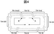
以下、図4を用いて、本実施例のドレインドライバ130の端子(バンプ電極)配置について説明する。なお、図4は、ドレインドライバ130の第1の基板(SUB1)と対向する面と反対側の面から見た図である。今、ドレインドライバ130の第1の基板(SUB1)と対向する面と反対の面から見て、時計回りの方向を第1の方向(図4の矢印Aに示す方向)、反時計回りを第2の方向(図4の矢印Bに示す方向)とするとき、ドレインドライバ130の回路基板側の長辺に沿って形成される端子の中央部に、電源電圧(Vdd)の入力端子群(TA−VI)が配置され、電源電圧(Vdgn)の入力端子群(TA−VI)から第1の方向に、階調基準電圧(Vref)の入力端子群(TA−VreI)、表示データ(DATA)の入力端子群(TA−DI)、制御信号の入力端子群(TA−SI)が順番に配置される。
また、電源電圧(Vdgn)の入力端子群(TA−VI)から第2の方向に、階調基準電圧(Vref)の出力端子群(TA−VreO)、表示データ(DATA)の出力端子群(TA−DO)、制御信号の出力端子群(TA−SO)が順番に配置される。
即ち、電源電圧(Vdgn)の入力端子群(TA−VI)、階調基準電圧(Vref)の入力端子群(TA−VreI)、および階調基準電圧(Vref)の出力端子群(TA−VreO)は、ドレインドライバ130の回路基板側の長辺に沿って配置され、表示データ(DATA)の入力端子群(TA−DI)は、ドレインドライバ130の表示制御回路側の短辺に沿って配置され、表示データ(DATA)の出力端子群(TA−DO)は、ドレインドライバ130の表示制御回路110と反対側の短辺に沿って配置され、制御信号の入力端子群(TA−SI)は、ドレインドライバ130の回路基板(FPC)と反対側で、表示制御回路側の長辺に沿って配置され、制御信号の出力端子群(TA−SO)は、ドレインドライバ130の回路基板(FPC)と反対側で、表示制御回路110と反対側の長辺に沿って配置される。
なお、図4において、TA−Oは映像電圧出力端子群であり、映像電圧出力端子群(TA−O)の端子は、それぞれ対応する映像線(DL)に接続される。
これにより、表示制御回路110とドレインドライバ130を、第1の基板(SUB1)上に実装し、各ドレインドライバ間でデータ転送を行うような液晶表示装置において、第1の基板(SUB1)上で配線を交差させることなく、配線を行うことができるので、安価でコンパクトな液晶表示装置を実現することが可能となる。Hereinafter, the terminal (bump electrode) arrangement of the
Further, in the second direction from the input terminal group (TA-VI) of the power supply voltage (Vdgn), the output terminal group (TA-VreO) of the gradation reference voltage (Vref) and the output terminal group of display data (DATA) ( TA-DO) and control signal output terminals (TA-SO) are arranged in order.
That is, the input terminal group (TA-VI) for the power supply voltage (Vdgn), the input terminal group (TA-VreI) for the gradation reference voltage (Vref), and the output terminal group (TA-VreO) for the gradation reference voltage (Vref). ) Is arranged along the long side of the
In FIG. 4, TA-O is a video voltage output terminal group, and the terminals of the video voltage output terminal group (TA-O) are respectively connected to the corresponding video lines (DL).
Accordingly, in the liquid crystal display device in which the
図3は、本実施例のより具体的な構成の他の例を説明するための図である。
図3に示す例では、回路基板(FPC)上に階調基準電圧生成回路(DAC)とEEPROM(EROM)とが実装される。さらに、階調基準電圧生成回路(DAC)と、EEPROM(EROM)と、表示制御回路110とを、I2Cバスなどのシリアルバス(S−BUS)で接続する。ここで、EEPROM(EROM)には、階調基準電圧データが保持される。
電源が投入されると、表示制御回路110は、EEPROM(EROM)の階調基準データを読み込み、当該読み込んだ階調基準電圧データを、階調基準電圧生成回路(DAC)内のレジスタ66に書き込む。
階調基準電圧生成回路(DAC)は、レジスタ66に書き込まれた階調基準電圧データに対応した階調基準電圧(Vref)を各ドレインドライバ130に供給する。
図3に示す例では、例えば、液晶表示パネルの階調−輝度特性に合わせて、最適な階調基準電圧を生成することが可能となる。FIG. 3 is a diagram for explaining another example of a more specific configuration of the present embodiment.
In the example shown in FIG. 3, a gradation reference voltage generation circuit (DAC) and an EEPROM (EROM) are mounted on a circuit board (FPC). Further, the gradation reference voltage generation circuit (DAC), the EEPROM (EROM), and the
When the power is turned on, the
The gradation reference voltage generation circuit (DAC) supplies a gradation reference voltage (Vref) corresponding to the gradation reference voltage data written in the
In the example shown in FIG. 3, for example, it is possible to generate an optimum gradation reference voltage in accordance with the gradation-luminance characteristics of the liquid crystal display panel.
図5は、図3に示す階調基準電圧生成回路(DAC)の一例を示す図である。
図5に示す階調基準電圧生成回路(DAC)は、VRinの電圧と接地電圧(GND)との間に接続される抵抗分圧回路で構成した例を示す図である。
V1〜V12の階調基準電圧は、分圧抵抗の比により設定され、抵抗分圧回路の出力は、バッファ回路63により、電流増幅されてドレインドライバ130の階調電圧生成回路に出力される。
ここで、図5では、分圧抵抗を、RBn−1、RBn−2、RBn−3の3つの抵抗で構成し、その中の一つを選択回路65で選択する。そして、表示制御回路110からレジスタ66に格納された階調基準電圧データに基づき、選択回路65を制御し、選択回路65で選択する抵抗を切り替えることにより、各ドレインドライバ130に出力する階調基準電圧(Vref)の電圧値を変更する。
一般に、階調基準電圧生成回路(DAC)と、EEPROM(EROM)は、表示制御回路110やドレインドライバ130に比べると、小さな半導体チップ(IC)で構成され、かつ安価なパッケージ品が主流なので、これらは第1の基板(SUB1)上に実装するよりも回路基板(FPC)上に実装したほうが、低コストで実現することが可能である。
なお、前述の説明では、本発明を液晶表示装置に適用した実施例について説明したが、本発明はこれに限定されるものではなく、本発明は、有機ELなどの大型高精細パネルを備える表示装置全てに適用可能である。
以上、本発明者によってなされた発明を、前記実施例に基づき具体的に説明したが、本発明は、前記実施例に限定されるものではなく、その要旨を逸脱しない範囲において種々変更可能であることは勿論である。FIG. 5 is a diagram illustrating an example of the gradation reference voltage generation circuit (DAC) illustrated in FIG.
The gradation reference voltage generation circuit (DAC) shown in FIG. 5 is a diagram showing an example of a resistor voltage dividing circuit connected between the voltage of VRin and the ground voltage (GND).
The gradation reference voltages V1 to V12 are set by the ratio of the voltage dividing resistors, and the output of the resistance voltage dividing circuit is current-amplified by the
Here, in FIG. 5, the voltage dividing resistor is configured by three resistors RBn−1, RBn−2 and RBn−3, and one of them is selected by the
In general, the gray scale reference voltage generation circuit (DAC) and the EEPROM (EROM) are configured by a small semiconductor chip (IC) and are inexpensive package products as compared with the
In the above description, the embodiment in which the present invention is applied to the liquid crystal display device has been described. However, the present invention is not limited to this, and the present invention is a display including a large-sized high-definition panel such as an organic EL. Applicable to all devices.
As mentioned above, the invention made by the present inventor has been specifically described based on the above embodiments. However, the present invention is not limited to the above embodiments, and various modifications can be made without departing from the scope of the invention. Of course.
63 バッファ回路
65 選択回路(スイッチ回路)
66 レジスタ
100 液晶表示パネル
110 表示制御回路(タイミングコントローラ)
120 電源回路
130 ドレインドライバ
131 電源ライン
132 表示データ・制御信号
133 階調基準電圧
140 ゲートドライバ
141 制御信号
142 電源配線
FPC フレキシブル配線基板
SUB1 第1の基板
SUB1 第2の基板
PIX 画素電極
TFT 薄膜トランジスタ
GL 走査線(またはゲート線)
DL 映像線(またはドレイン線、ソース線)
CLC 液晶容量
Cadd 保持容量
CT 対向電極
DAC 階調基準電圧生成回路
S−BUS シリアルバス
EROM EEPROM63
66
DESCRIPTION OF
DL video line (or drain line, source line)
CLC Liquid crystal capacitance Cadd Holding capacitance CT Counter electrode DAC Gray scale reference voltage generation circuit S-BUS Serial bus EROM EEPROM
Claims (8)
Translated fromJapanese各画素に映像電圧を供給する複数の駆動回路と、
前記複数の駆動回路を制御駆動する表示制御回路とを備える表示装置であって、
前記表示パネルは、少なくとも第1の基板を有し、
前記複数の駆動回路および前記表示制御回路は、前記第1の基板の一方の長辺の周辺部に実装され、
前記第1の基板の一方の長辺には、回路基板が接続され、
前記各駆動回路は、前記第1の基板と対向する面に、電源電圧が入力される電源電圧入力端子群と、階調基準電圧が入力される階調基準電圧入力端子群と、前記階調基準電圧を出力する階調基準電圧出力端子群とを有し、
前記電源電圧入力端子群、前記階調基準電圧入力端子群、および前記階調基準電圧出力端子群は、前記各駆動回路の前記回路基板側の長辺に沿って配置され、
前記電源電圧入力端子群は、前記階調基準電圧入力端子群と前記階調基準電圧出力端子群との間に配置され、
前記電源電圧入力端子群の前記表示制御回路側には、前記階調基準電圧入力端子群が配置され、
前記電源電圧入力端子群の前記表示制御回路と反対側には、前記階調基準電圧出力端子群が配置され、
前記各駆動回路の前記電源電圧入力端子群には、前記回路基板を介して電源電圧が入力され、
先頭の前記駆動回路の前記階調基準電圧入力端子群には、前記回路基板を介して階調基準電圧が入力され、
先頭以外の前記駆動回路には、前段の駆動回路の前記階調基準電圧出力端子群から出力される階調基準電圧が入力されることを特徴とする表示装置。A display panel having a plurality of pixels;
A plurality of drive circuits for supplying a video voltage to each pixel;
A display control circuit that controls and drives the plurality of drive circuits,
The display panel has at least a first substrate,
The plurality of drive circuits and the display control circuit are mounted on a peripheral portion of one long side of the first substrate,
A circuit board is connected to one long side of the first board,
Each of the driving circuits includes a power supply voltage input terminal group to which a power supply voltage is input, a grayscale reference voltage input terminal group to which a grayscale reference voltage is input, and the grayscale on a surface facing the first substrate. Gradation reference voltage output terminal group for outputting a reference voltage,
The power supply voltage input terminal group, the gradation reference voltage input terminal group, and the gradation reference voltage output terminal group are arranged along the long side of the drive circuit on the circuit board side,
The power supply voltage input terminal group is disposed between the gradation reference voltage input terminal group and the gradation reference voltage output terminal group,
The gradation reference voltage input terminal group is disposed on the display control circuit side of the power supply voltage input terminal group,
The gradation reference voltage output terminal group is disposed on the opposite side of the power supply voltage input terminal group from the display control circuit,
A power supply voltage is input to the power supply voltage input terminal group of each drive circuit via the circuit board,
A gradation reference voltage is input to the gradation reference voltage input terminal group of the leading drive circuit via the circuit board,
The display device characterized in that a gradation reference voltage output from the gradation reference voltage output terminal group of the preceding stage drive circuit is input to the drive circuits other than the head.
前記各駆動回路の前記第1の基板と対向する面と反対側の面から見て時計回り方向を第1の方向、反時計回りを第2の方向とするとき、前記表示データ入力端子群は、前記第1の方向において前記階調基準電圧出力端子群よりも先に配置され、
前記表示データ出力端子群は、前記第2の方向において前記階調基準電圧出力端子群よりも先に配置され、
先頭の前記駆動回路の前記表示データ入力端子群には、前記表示制御回路から出力される表示データが入力され、
先頭以外の前記駆動回路には、前段の駆動回路の前記表示データ出力端子群から出力される表示データが入力されることを特徴とする請求項1または請求項2に記載の表示装置。Each of the drive circuits has a display data input terminal group and a display data output terminal group on a surface facing the first substrate,
When the clockwise direction when viewed from the surface opposite to the surface facing the first substrate of each drive circuit is the first direction and the counterclockwise direction is the second direction, the display data input terminal group is , Arranged in the first direction before the grayscale reference voltage output terminal group,
The display data output terminal group is disposed before the gradation reference voltage output terminal group in the second direction,
Display data output from the display control circuit is input to the display data input terminal group of the leading drive circuit,
3. The display device according to claim 1, wherein display data output from the display data output terminal group of the preceding drive circuit is input to the drive circuits other than the head. 4.
前記制御信号入力端子群は、前記第1の方向において前記表示データ入力端子群よりも先に配置され、
前記制御信号出力端子群は、前記第2の方向において前記表示データ出力端子群よりも先に配置され、
先頭の前記駆動回路の前記制御信号入力端子群には、前記表示制御回路から出力される制御信号が入力され、
先頭以外の前記駆動回路には、前段の駆動回路の前記制御信号出力端子群から出力される制御信号が入力されることを特徴とする請求項3に記載の表示装置。Each of the driving circuits has a control signal input terminal group and a control signal output terminal group on a surface facing the first substrate,
The control signal input terminal group is disposed before the display data input terminal group in the first direction,
The control signal output terminal group is arranged before the display data output terminal group in the second direction,
A control signal output from the display control circuit is input to the control signal input terminal group of the leading drive circuit,
The display device according to claim 3, wherein a control signal output from the control signal output terminal group of the preceding drive circuit is input to the drive circuits other than the head.
前記表示データ出力端子群は、前記各駆動回路の前記表示制御回路と反対側の短辺に沿って配置され、
前記制御信号入力端子群は、前記各駆動回路の前記回路基板と反対側で、前記表示制御回路側の長辺に沿って配置され、
前記制御信号出力端子群は、前記各駆動回路の前記回路基板と反対側で、前記表示制御回路と反対側の長辺に沿って配置されることを特徴とする請求項4に記載の表示装置。The display data input terminal group is disposed along a short side of the drive circuit on the display control circuit side,
The display data output terminal group is disposed along a short side opposite to the display control circuit of each drive circuit,
The control signal input terminal group is disposed along the long side on the display control circuit side on the side opposite to the circuit board of each drive circuit,
5. The display device according to claim 4, wherein the control signal output terminal group is disposed along a long side opposite to the display control circuit on a side opposite to the circuit board of each of the drive circuits. .
前記階調基準電圧生成回路は、レジスタを有し、
前記表示制御回路は、前記格納手段に格納されている前記階調基準データを読み込み、前記階調基準電圧生成回路に出力し、
前記階調基準電圧生成回路は、前記表示制御回路から入力された前記階調基準電圧データを前記レジスタに格納し、当該レジスタに格納した階調基準電圧データに基づき階調基準電圧を生成することを特徴とする請求項6に記載の表示装置。The circuit board is mounted with storage means for storing gradation reference voltage data,
The gradation reference voltage generation circuit has a register,
The display control circuit reads the gradation reference data stored in the storage means, and outputs the gradation reference data to the gradation reference voltage generation circuit.
The gradation reference voltage generation circuit stores the gradation reference voltage data input from the display control circuit in the register, and generates a gradation reference voltage based on the gradation reference voltage data stored in the register. The display device according to claim 6.
前記表示パネルは、第1の基板と、第2の基板と、前記第1の基板と前記第2の基板との間に挟持される液晶層とを有する液晶表示パネルであることを特徴とする請求項1ないし請求項7のいずれか1項に記載の表示装置。The display device is a liquid crystal display device,
The display panel is a liquid crystal display panel having a first substrate, a second substrate, and a liquid crystal layer sandwiched between the first substrate and the second substrate. The display device according to any one of claims 1 to 7.
Priority Applications (2)
| Application Number | Priority Date | Filing Date | Title |
|---|---|---|---|
| JP2008003849AJP2009168867A (en) | 2008-01-11 | 2008-01-11 | Display device |
| US12/318,269US8085231B2 (en) | 2008-01-11 | 2008-12-23 | Display device |
Applications Claiming Priority (1)
| Application Number | Priority Date | Filing Date | Title |
|---|---|---|---|
| JP2008003849AJP2009168867A (en) | 2008-01-11 | 2008-01-11 | Display device |
Publications (1)
| Publication Number | Publication Date |
|---|---|
| JP2009168867Atrue JP2009168867A (en) | 2009-07-30 |
Family
ID=40850243
Family Applications (1)
| Application Number | Title | Priority Date | Filing Date |
|---|---|---|---|
| JP2008003849APendingJP2009168867A (en) | 2008-01-11 | 2008-01-11 | Display device |
Country Status (2)
| Country | Link |
|---|---|
| US (1) | US8085231B2 (en) |
| JP (1) | JP2009168867A (en) |
Cited By (3)
| Publication number | Priority date | Publication date | Assignee | Title |
|---|---|---|---|---|
| WO2012033012A1 (en)* | 2010-09-09 | 2012-03-15 | シャープ株式会社 | Display device |
| US9343145B2 (en) | 2008-01-15 | 2016-05-17 | Micron Technology, Inc. | Memory cells, memory cell programming methods, memory cell reading methods, memory cell operating methods, and memory devices |
| US11158252B2 (en) | 2018-08-08 | 2021-10-26 | Joled Inc. | Circuit board and display device |
Families Citing this family (4)
| Publication number | Priority date | Publication date | Assignee | Title |
|---|---|---|---|---|
| CN104737218B (en)* | 2012-11-16 | 2017-03-01 | 夏普株式会社 | Driver module, display device and multi-display device |
| JP2015079187A (en)* | 2013-10-18 | 2015-04-23 | シナプティクス・ディスプレイ・デバイス株式会社 | Display device and display driver |
| CN103680437A (en)* | 2013-11-11 | 2014-03-26 | 京东方科技集团股份有限公司 | Current acquisition device, drive unit and method, array substrate and its preparation method |
| CN105185325A (en)* | 2015-08-12 | 2015-12-23 | 深圳市华星光电技术有限公司 | Liquid crystal display driving system and driving method |
Citations (5)
| Publication number | Priority date | Publication date | Assignee | Title |
|---|---|---|---|---|
| JPS61172348A (en)* | 1985-01-28 | 1986-08-04 | Hitachi Ltd | Lsi element for liquid crystal drive |
| JP2001306040A (en)* | 2000-02-18 | 2001-11-02 | Hitachi Ltd | Liquid crystal display |
| JP2001331150A (en)* | 2000-05-18 | 2001-11-30 | Hitachi Ltd | Liquid crystal display |
| JP2005326790A (en)* | 2004-05-17 | 2005-11-24 | Nec Saitama Ltd | Liquid crystal display, driving method used for the liquid crystal display, and electronic equipent equipped with the liquid crystal display |
| JP2007243128A (en)* | 2005-06-30 | 2007-09-20 | Seiko Epson Corp | Integrated circuit device and electronic apparatus |
Family Cites Families (10)
| Publication number | Priority date | Publication date | Assignee | Title |
|---|---|---|---|---|
| JP3495960B2 (en)* | 1999-12-10 | 2004-02-09 | シャープ株式会社 | Gray scale display reference voltage generating circuit and liquid crystal driving device using the same |
| JP2003280615A (en)* | 2002-01-16 | 2003-10-02 | Sharp Corp | Gray scale reference voltage generating circuit and liquid crystal display device using the same |
| US20040134988A1 (en)* | 2003-01-09 | 2004-07-15 | Hand Held Products, Inc. | Analog-to-digital converter with automatic range and sensitivity adjustment |
| KR100603457B1 (en)* | 2003-07-18 | 2006-07-20 | 엘지전자 주식회사 | Power supply device for improving power factor and driving method thereof |
| GB0318611D0 (en)* | 2003-08-08 | 2003-09-10 | Koninkl Philips Electronics Nv | Circuit for signal amplification and use of the same in active matrix devices |
| JP2005157321A (en)* | 2003-11-07 | 2005-06-16 | Renesas Technology Corp | Semiconductor device and method for testing semiconductor device |
| JP4412027B2 (en)* | 2004-03-29 | 2010-02-10 | 日本電気株式会社 | Amplifier circuit and display device |
| JP2006178283A (en)* | 2004-12-24 | 2006-07-06 | Matsushita Electric Ind Co Ltd | Current drive device and current drive method |
| KR20070007591A (en)* | 2005-07-11 | 2007-01-16 | 삼성전자주식회사 | Voltage generator circuit of flat panel display device |
| KR100751368B1 (en)* | 2006-02-20 | 2007-08-22 | 삼성에스디아이 주식회사 | Driving device for display panel and driving method thereof |
- 2008
- 2008-01-11JPJP2008003849Apatent/JP2009168867A/enactivePending
- 2008-12-23USUS12/318,269patent/US8085231B2/enactiveActive
Patent Citations (5)
| Publication number | Priority date | Publication date | Assignee | Title |
|---|---|---|---|---|
| JPS61172348A (en)* | 1985-01-28 | 1986-08-04 | Hitachi Ltd | Lsi element for liquid crystal drive |
| JP2001306040A (en)* | 2000-02-18 | 2001-11-02 | Hitachi Ltd | Liquid crystal display |
| JP2001331150A (en)* | 2000-05-18 | 2001-11-30 | Hitachi Ltd | Liquid crystal display |
| JP2005326790A (en)* | 2004-05-17 | 2005-11-24 | Nec Saitama Ltd | Liquid crystal display, driving method used for the liquid crystal display, and electronic equipent equipped with the liquid crystal display |
| JP2007243128A (en)* | 2005-06-30 | 2007-09-20 | Seiko Epson Corp | Integrated circuit device and electronic apparatus |
Cited By (3)
| Publication number | Priority date | Publication date | Assignee | Title |
|---|---|---|---|---|
| US9343145B2 (en) | 2008-01-15 | 2016-05-17 | Micron Technology, Inc. | Memory cells, memory cell programming methods, memory cell reading methods, memory cell operating methods, and memory devices |
| WO2012033012A1 (en)* | 2010-09-09 | 2012-03-15 | シャープ株式会社 | Display device |
| US11158252B2 (en) | 2018-08-08 | 2021-10-26 | Joled Inc. | Circuit board and display device |
Also Published As
| Publication number | Publication date |
|---|---|
| US8085231B2 (en) | 2011-12-27 |
| US20090179922A1 (en) | 2009-07-16 |
Similar Documents
| Publication | Publication Date | Title |
|---|---|---|
| CN111048025B (en) | Shift register and display device using the same | |
| KR102169169B1 (en) | Display device and method for driving the same | |
| US9910329B2 (en) | Liquid crystal display device for cancelling out ripples generated the common electrode | |
| JP5043415B2 (en) | Display device | |
| CN1940658B (en) | Liquid crystal display and manufacturing method thereof | |
| US20070085800A1 (en) | Liquid crystal display driving device that reduces crosstalk | |
| KR20170080002A (en) | Array substrate and display device including the same | |
| KR20150127500A (en) | Source driver and Display device comprising thereof | |
| KR102684634B1 (en) | Display device | |
| JP2009168867A (en) | Display device | |
| JP2003107423A (en) | Liquid crystal display device and method of manufacturing liquid crystal display device | |
| CN116069179A (en) | Touch driver circuit, driving method, and driver device for touch display device | |
| KR20160033351A (en) | Display device | |
| KR20170062573A (en) | Display device | |
| CN101236722A (en) | Display device and driving method thereof | |
| JP4241858B2 (en) | Liquid crystal device and electronic device | |
| US7782282B2 (en) | Display device and driving method thereof | |
| JP5022651B2 (en) | Display device | |
| CN101593499A (en) | Display device | |
| CN101241678A (en) | Display device driving device and driving method thereof | |
| JP4595008B2 (en) | Display device, electronic device, electronic system | |
| JP4283431B2 (en) | Liquid crystal display | |
| JP4516307B2 (en) | Liquid crystal display | |
| KR20110032837A (en) | Liquid crystal display | |
| JP5046230B2 (en) | Liquid crystal device and electronic device |
Legal Events
| Date | Code | Title | Description |
|---|---|---|---|
| A621 | Written request for application examination | Free format text:JAPANESE INTERMEDIATE CODE: A621 Effective date:20101215 | |
| A711 | Notification of change in applicant | Free format text:JAPANESE INTERMEDIATE CODE: A712 Effective date:20110218 | |
| RD03 | Notification of appointment of power of attorney | Free format text:JAPANESE INTERMEDIATE CODE: A7423 Effective date:20110218 | |
| A131 | Notification of reasons for refusal | Free format text:JAPANESE INTERMEDIATE CODE: A131 Effective date:20120731 | |
| A977 | Report on retrieval | Free format text:JAPANESE INTERMEDIATE CODE: A971007 Effective date:20120801 | |
| A521 | Written amendment | Free format text:JAPANESE INTERMEDIATE CODE: A523 Effective date:20120921 | |
| A02 | Decision of refusal | Free format text:JAPANESE INTERMEDIATE CODE: A02 Effective date:20121016 |