JP2009147512A - Pre-emphasis circuit - Google Patents
Pre-emphasis circuitDownload PDFInfo
- Publication number
- JP2009147512A JP2009147512AJP2007320771AJP2007320771AJP2009147512AJP 2009147512 AJP2009147512 AJP 2009147512AJP 2007320771 AJP2007320771 AJP 2007320771AJP 2007320771 AJP2007320771 AJP 2007320771AJP 2009147512 AJP2009147512 AJP 2009147512A
- Authority
- JP
- Japan
- Prior art keywords
- emphasis
- differential
- transconductance amplifier
- output
- pass filter
- Prior art date
- Legal status (The legal status is an assumption and is not a legal conclusion. Google has not performed a legal analysis and makes no representation as to the accuracy of the status listed.)
- Granted
Links
Images


Landscapes
- Dc Digital Transmission (AREA)
- Cable Transmission Systems, Equalization Of Radio And Reduction Of Echo (AREA)
- Logic Circuits (AREA)
- Networks Using Active Elements (AREA)
- Amplifiers (AREA)
Abstract
Translated fromJapaneseDescription
Translated fromJapanese本発明は、信号の変化点で振幅を大きくするプリエンファシス回路に関し、特に簡単な構成でプリエンファシス信号を生成することが可能なプリエンファシス回路に関する。 The present invention relates to a pre-emphasis circuit that increases the amplitude at a signal change point, and more particularly to a pre-emphasis circuit that can generate a pre-emphasis signal with a simple configuration.
従来の信号の変化点で振幅を大きくするプリエンファシス回路に関連する先行技術文献としては次のようなものがある。 Prior art documents related to a pre-emphasis circuit in which the amplitude is increased at the signal change point are as follows.
図7は損失を有する伝送線路における信号の送受信を説明する説明図であり、図7において、1は信号を送信する送信器、2は信号を受信する受信器、3は損失を有する伝送線路である。送信器1は伝送線路3の一端に接続され、受信器2は伝送線路3の他端に接続される。 FIG. 7 is an explanatory diagram for explaining transmission / reception of a signal in a transmission line having a loss. In FIG. 7, 1 is a transmitter for transmitting a signal, 2 is a receiver for receiving a signal, and 3 is a transmission line having a loss. is there. The transmitter 1 is connected to one end of the transmission line 3, and the receiver 2 is connected to the other end of the transmission line 3.
ここで、図7に示す伝送線路における信号の送受信を説明する。送信器1が、図7(a)に示すような矩形波信号を送信信号として伝送線路3に送信した場合、伝送線路3の損失によって信号の変化点が丸められて、受信器2では、図7(b)に示すような受信信号が受信される。 Here, transmission and reception of signals in the transmission line shown in FIG. 7 will be described. When the transmitter 1 transmits a rectangular wave signal as shown in FIG. 7A as a transmission signal to the transmission line 3, the signal change point is rounded due to the loss of the transmission line 3. A received signal as shown in 7 (b) is received.
一方、送信器1が、図7(c)に示すような信号の変化点で振幅を大きくしたプリエンファシス信号を送信信号として伝送線路3に送信した場合、伝送線路3の損失によって信号の強調部分が丸められて、受信器2では、図7(d)に示すようなきれいな矩形波信号が受信信号として受信される。 On the other hand, when the transmitter 1 transmits a pre-emphasis signal whose amplitude is increased at the signal change point as shown in FIG. 7C to the transmission line 3 as a transmission signal, the signal enhancement portion is caused by the loss of the transmission line 3. Is rounded, and the receiver 2 receives a clean rectangular wave signal as shown in FIG.
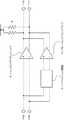
また、図8は「特許文献5」に記載された従来のプリエンファシス回路の一例を示す構成ブロック図である。図8において、4及び6は差動信号を後段に出力するドライバ回路、5は入力された差動信号を遅延させる遅延回路、7は2つの差動信号を減算して差動信号として出力する減算回路、100及び101は差動入力信号、102及び103は差動出力信号である。 FIG. 8 is a block diagram showing an example of a conventional pre-emphasis circuit described in “Patent Document 5”. In FIG. 8, 4 and 6 are driver circuits that output differential signals to the subsequent stage, 5 is a delay circuit that delays the inputted differential signals, and 7 is a subtracted two differential signals and outputs them as differential signals. Subtraction circuits, 100 and 101 are differential input signals, and 102 and 103 are differential output signals.
差動入力信号100及び101はドライバ回路4及び遅延回路5の差動入力端子にそれぞれ印加され、遅延回路5の差動出力はドライバ回路6の差動入力端子にそれぞれ接続される。 The
また、ドライバ回路4及びドライバ回路6の差動出力は減算回路7の2つの差動入力端子にそれぞれ接続され、減算回路7の差動出力端子からは差動出力信号102及び103がそれぞれ出力される。 The differential outputs of the driver circuit 4 and the driver circuit 6 are connected to the two differential input terminals of the subtractor circuit 7, respectively, and
ここで、図8に示す従来例の動作を図9を用いて説明する。図9は従来のプリエンファシス回路の動作を説明するタイミング図である。 Here, the operation of the conventional example shown in FIG. 8 will be described with reference to FIG. FIG. 9 is a timing chart for explaining the operation of the conventional pre-emphasis circuit.
差動入力信号100及び101はドライバ回路4を介して減算回路7に印加され、一方、遅延回路5で遅延された差動入力信号100及び101はドライバ回路6を介して減算回路7に印加され、その差分が差動出力信号102及び103として出力される。 The
例えば、ドライバ回路4の出力信号とドライバ回路6の出力信号が図9(a)及び(b)に示すタイミングであった場合、図9(c)に示すような信号の変化点で振幅を大きくされたプリエンファシス信号が減算回路7の出力信号として出力される。 For example, when the output signal of the driver circuit 4 and the output signal of the driver circuit 6 have the timing shown in FIGS. 9A and 9B, the amplitude is increased at the signal change point as shown in FIG. 9C. The pre-emphasis signal thus output is output as an output signal of the subtraction circuit 7.
この結果、差動入力信号を2分割すると共に一方の差動入力信号を遅延させ両者の差分を求めることにより、プリエンファシス信号を生成することができる。 As a result, the pre-emphasis signal can be generated by dividing the differential input signal into two and delaying one differential input signal to obtain the difference between the two.
しかし、図8に示す従来例では、構成要素として素子数が多く構成が複雑である遅延回路を用いているため、チップ面積が大きくなってしまうと言った問題点があった。 However, the conventional example shown in FIG. 8 has a problem that the chip area increases because a delay circuit having a large number of elements and a complicated configuration is used as a component.
また、プリエンファシス強度を変化させる場合、差動入力信号と遅延された差動入力信号を混合(減算)する割合を調整することによって対応可能であるものの、直流レベルが混合の割合に起因して変化してしまうと言った問題点があった。
従って本発明が解決しようとする課題は、簡単な構成でプリエンファシス信号を生成することが可能なプリエンファシス回路を実現することにある。Also, when changing the pre-emphasis intensity, it can be handled by adjusting the ratio of mixing (subtracting) the differential input signal and the delayed differential input signal, but the DC level is caused by the mixing ratio. There was a problem that it would change.
Therefore, the problem to be solved by the present invention is to realize a pre-emphasis circuit capable of generating a pre-emphasis signal with a simple configuration.
このような課題を達成するために、本発明のうち請求項1記載の発明は、
信号の変化点で振幅を大きくするプリエンファシス回路において、
差動入力信号を差動電流出力に変換する第1のトランスコンダクタンスアンプと、ハイパスフィルタ回路と、このハイパスフィルタ回路を介した前記差動入力信号を差動電流出力に変換する第2のトランスコンダクタンスアンプと、2つの前記差動電流出力をそれぞれ加算して電圧変換する第1及び第2の抵抗とを備えたことにより、簡単な構成でプリエンファシス信号を生成することが可能になる。In order to achieve such a problem, the invention according to claim 1 of the present invention is:
In the pre-emphasis circuit that increases the amplitude at the signal change point,
A first transconductance amplifier that converts a differential input signal into a differential current output, a high-pass filter circuit, and a second transconductance that converts the differential input signal through the high-pass filter circuit into a differential current output By providing the amplifier and the first and second resistors for adding and converting the two differential current outputs, respectively, it is possible to generate a pre-emphasis signal with a simple configuration.
請求項2記載の発明は、
請求項1記載の発明であるプリエンファシス回路において、
前記トランスコンダクタンスアンプが、
エミッタが相互に接続されそれぞれのコレクタから前記差動電流出力を出力する2つのトランジスタと、これらトランジスタのエミッタに接続された定電流源から構成されたことにより、簡単な構成でプリエンファシス信号を生成することが可能になる。The invention according to claim 2
In the pre-emphasis circuit according to the invention of claim 1,
The transconductance amplifier is
Pre-emphasis signals can be generated with a simple configuration by comprising two transistors whose emitters are connected to each other and outputting the differential current output from each collector, and a constant current source connected to the emitters of these transistors. It becomes possible to do.
請求項3記載の発明は、
信号の変化点で振幅を大きくするプリエンファシス回路において、
差動入力信号を差動電流出力に変換する第1のトランスコンダクタンスアンプと、ハイパスフィルタ回路と、このハイパスフィルタ回路を介した前記差動入力信号を差動電流出力に変換する第2のトランスコンダクタンスアンプと、2つの前記差動電流出力をそれぞれ加算して電圧変換する第1及び第2の抵抗と、前記第1及び第2の抵抗に出力電流を出力する直流レベル調整手段と、前記第2のトランスコンダクタンスアンプと前記直流レベル調整手段とに定電流を分配して供給するプリエンファシス強度調整手段とを備えたことにより、簡単な構成で直流レベルを変化させることなくプリエンファシス強度が可変であるプリエンファシス信号を生成することが可能になる。The invention described in claim 3
In the pre-emphasis circuit that increases the amplitude at the signal change point,
A first transconductance amplifier that converts a differential input signal into a differential current output, a high-pass filter circuit, and a second transconductance that converts the differential input signal through the high-pass filter circuit into a differential current output An amplifier, first and second resistors for voltage conversion by adding the two differential current outputs, DC level adjusting means for outputting an output current to the first and second resistors, and the second Pre-emphasis intensity adjusting means for distributing and supplying a constant current to the transconductance amplifier and the DC level adjusting means is provided, so that the pre-emphasis intensity is variable without changing the DC level with a simple configuration. A pre-emphasis signal can be generated.
請求項4記載の発明は、
請求項3記載の発明であるプリエンファシス回路において、
前記第1のトランスコンダクタンスアンプが、
エミッタが相互に接続されそれぞれのコレクタから前記差動電流出力を出力する2つのトランジスタと、これらトランジスタのエミッタに接続された定電流源から構成されたことにより、簡単な構成で直流レベルを変化させることなくプリエンファシス強度が可変であるプリエンファシス信号を生成することが可能になる。The invention according to claim 4
In the pre-emphasis circuit as claimed in claim 3,
The first transconductance amplifier is
The DC level is changed with a simple configuration by comprising two transistors whose emitters are connected to each other and outputting the differential current output from the respective collectors, and a constant current source connected to the emitters of these transistors. Without this, it is possible to generate a pre-emphasis signal having a variable pre-emphasis intensity.
請求項5記載の発明は、
請求項3記載の発明であるプリエンファシス回路において、
前記第2のトランスコンダクタンスアンプが、
エミッタが相互に接続されそれぞれのコレクタから前記差動電流出力を出力する2つのトランジスタとから構成されたことにより、簡単な構成で直流レベルを変化させることなくプリエンファシス強度が可変であるプリエンファシス信号を生成することが可能になる。The invention according to claim 5
In the pre-emphasis circuit as claimed in claim 3,
The second transconductance amplifier is
Pre-emphasis signal whose emitter emphasis is variable and the pre-emphasis intensity is variable without changing the DC level with a simple configuration by being composed of two transistors connected to each other and outputting the differential current output from each collector Can be generated.
請求項6記載の発明は、
請求項3記載の発明であるプリエンファシス回路において、
前記直流レベル調整手段が、
ベースにバイアス電圧が印加されエミッタが相互に接続されそれぞれのコレクタから前記第1及び第2の抵抗に出力電流を出力する2つのトランジスタとから構成されたことにより、簡単な構成で直流レベルを変化させることなくプリエンファシス強度が可変であるプリエンファシス信号を生成することが可能になる。The invention described in claim 6
In the pre-emphasis circuit as claimed in claim 3,
The DC level adjusting means is
The bias voltage is applied to the base, the emitters are connected to each other, and the two transistors that output the output current from the respective collectors to the first and second resistors are used to change the DC level with a simple configuration. Thus, it is possible to generate a pre-emphasis signal having a variable pre-emphasis intensity.
請求項7記載の発明は、
請求項3記載の発明であるプリエンファシス回路において、
前記プリエンファシス強度調整手段が、
ベースにそれぞれ制御信号が印加されエミッタが相互に接続されそれぞれのコレクタから前記第2のトランスコンダクタンスアンプと前記直流レベル調整手段とに電流を出力する2つのトランジスタと、これらトランジスタのエミッタに接続された定電流源から構成されたことにより、簡単な構成で直流レベルを変化させることなくプリエンファシス強度が可変であるプリエンファシス信号を生成することが可能になる。The invention described in claim 7
In the pre-emphasis circuit as claimed in claim 3,
The pre-emphasis intensity adjusting means is
Control transistors are applied to the bases, emitters are connected to each other, two transistors for outputting current from the respective collectors to the second transconductance amplifier and the DC level adjusting means, and connected to the emitters of these transistors With the configuration of the constant current source, it is possible to generate a pre-emphasis signal having a variable pre-emphasis intensity without changing the DC level with a simple configuration.
請求項8記載の発明は、
請求項1若しくは請求項3記載の発明であるプリエンファシス回路において、
前記ハイパスフィルタ回路が、
前記差動入力信号がそれぞれ一端に接続される2つの容量と、これら容量の他端がそれぞれ一端に接続される2つの抵抗と、これら抵抗の他端の両方が一端に接続される定電圧源とから構成されたことにより、簡単な構成で直流レベルを変化させることなくプリエンファシス強度が可変であるプリエンファシス信号を生成することが可能になる。The invention described in claim 8
In the pre-emphasis circuit according to the invention of claim 1 or claim 3,
The high-pass filter circuit is
Two capacitors each connected to one end of the differential input signal, two resistors each having the other end connected to one end, and a constant voltage source having both ends connected to the other end Thus, it is possible to generate a pre-emphasis signal with a variable pre-emphasis intensity without changing the DC level with a simple configuration.
請求項9記載の発明は、
請求項1若しくは請求項3記載の発明であるプリエンファシス回路において、
前記ハイパスフィルタ回路が、
周波数特性が可変なハイパスフィルタ回路であることにより、プリエンファシス時間が可変であるプリエンファシス信号を生成することが可能になる。The invention according to claim 9
In the pre-emphasis circuit according to the invention of claim 1 or claim 3,
The high-pass filter circuit is
By using a high-pass filter circuit with variable frequency characteristics, it is possible to generate a pre-emphasis signal with a variable pre-emphasis time.
請求項10記載の発明は、
請求項9記載の発明であるプリエンファシス回路において、
前記ハイパスフィルタ回路が、
前記差動入力信号がそれぞれ一端に接続される2つの容量と、これら容量の他端がそれぞれ一端に接続される2つの抵抗と、これら抵抗の他端の両方が一端に接続される定電圧源と、前記2つの容量のそれぞれに設けられスイッチ回路によって並列に接続/非接続される1つ以上の容量とから構成されたことにより、プリエンファシス時間が可変であるプリエンファシス信号を生成することが可能になる。The invention according to claim 10 is:
In the pre-emphasis circuit according to the invention of claim 9,
The high-pass filter circuit is
Two capacitors each connected to one end of the differential input signal, two resistors each having the other end connected to one end, and a constant voltage source having both ends connected to the other end And one or more capacitors provided in each of the two capacitors and connected / disconnected in parallel by a switch circuit, thereby generating a pre-emphasis signal having a variable pre-emphasis time. It becomes possible.
本発明によれば次のような効果がある。
請求項1,2及び請求項8の発明によれば、差動入力信号を2分割すると共に一方の差動入力信号を第1のトランスコンダクタンスアンプで差動電流出力に変換し、他方の差動入力信号をハイパスフィルタ回路を介して第2のトランスコンダクタンスアンプで差動電流出力に変換し、2つの差動電流出力を加算して電圧変換することにより、簡単な構成でプリエンファシス信号を生成することが可能になる。The present invention has the following effects.
According to the first, second, and eighth aspects of the present invention, the differential input signal is divided into two, one differential input signal is converted into a differential current output by the first transconductance amplifier, and the other differential A pre-emphasis signal is generated with a simple configuration by converting the input signal to a differential current output by a second transconductance amplifier via a high-pass filter circuit and adding the two differential current outputs for voltage conversion. It becomes possible.
また、請求項3,4,5,6,7及び請求項8の発明によれば、差動入力信号を2分割して、一方の差動入力信号を第1のトランスコンダクタンスアンプで差動電流出力に変換し、他方の差動入力信号をハイパスフィルタ回路を介して第2のトランスコンダクタンスアンプで差動電流出力に変換し、2つの差動電流出力を加算して電圧変換すると共にプリエンファシス強度調整手段が定電流を第2のトランスコンダクタンスアンプと直流レベル調整手段とに分配することにより、簡単な構成で直流レベルを変化させることなくプリエンファシス強度が可変であるプリエンファシス信号を生成することが可能になる。 According to the third, fourth, fifth, sixth, seventh, and eighth aspects of the present invention, the differential input signal is divided into two, and one differential input signal is converted into a differential current by the first transconductance amplifier. The other differential input signal is converted to a differential current output by a second transconductance amplifier via a high-pass filter circuit, and the two differential current outputs are summed and converted to voltage, and the pre-emphasis intensity The adjustment unit distributes the constant current to the second transconductance amplifier and the DC level adjustment unit, thereby generating a pre-emphasis signal having a variable pre-emphasis intensity without changing the DC level with a simple configuration. It becomes possible.
また、請求項9及び請求項10の発明によれば、差動入力信号を2分割して、一方の差動入力信号を第1のトランスコンダクタンスアンプで差動電流出力に変換し、他方の差動入力信号をハイパスフィルタ回路を介して第2のトランスコンダクタンスアンプで差動電流出力に変換し、2つの差動電流出力を加算して電圧変換すると共に周波数特性(カットオフ周波数)が可変なハイパスフィルタ回路を用いることにより、プリエンファシス時間が可変であるプリエンファシス信号を生成することが可能になる。 According to the ninth and tenth aspects of the present invention, the differential input signal is divided into two parts, one differential input signal is converted into a differential current output by the first transconductance amplifier, and the other difference A high-pass that converts a dynamic input signal into a differential current output through a high-pass filter circuit by a second transconductance amplifier, adds two differential current outputs, converts the voltage, and has variable frequency characteristics (cut-off frequency) By using the filter circuit, a pre-emphasis signal having a variable pre-emphasis time can be generated.
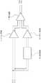
以下本発明を図面を用いて詳細に説明する。図1は本発明に係るプリエンファシス回路の一実施例を示す構成ブロック図である。 Hereinafter, the present invention will be described in detail with reference to the drawings. FIG. 1 is a block diagram showing a pre-emphasis circuit according to an embodiment of the present invention.
図1において、8及び10は差動入出力のトランスコンダクタンスアンプ、9は差動入出力のハイパスフィルタ回路、11及び12は2つのトランスコンダクタンスアンプからの差動電流出力をそれぞれ加算して電圧変換する抵抗、104及び105は差動入力信号、106及び107は差動出力信号である。 In FIG. 1, 8 and 10 are differential input / output transconductance amplifiers, 9 is a differential input / output high-pass filter circuit, and 11 and 12 are voltage conversions by adding differential current outputs from two transconductance amplifiers, respectively.
差動入力信号100及び101はトランスコンダクタンスアンプ8及びハイパスフィルタ回路9の差動入力端子にそれぞれ印加され、ハイパスフィルタ回路9の差動出力はトランスコンダクタンスアンプ10の差動入力端子にそれぞれ接続される。 The differential input signals 100 and 101 are applied to the differential input terminals of the transconductance amplifier 8 and the high-pass filter circuit 9, respectively, and the differential outputs of the high-pass filter circuit 9 are connected to the differential input terminals of the transconductance amplifier 10, respectively. .
また、トランスコンダクタンスアンプ8及びトランスコンダクタンスアンプ10の差動電流出力は抵抗11及び12の一端にそれぞれ接続されると共に差動出力信号106及び107として出力される。最後に、抵抗11及び12の他端は正電圧源に接続される。 The differential current outputs of the transconductance amplifier 8 and the transconductance amplifier 10 are connected to one ends of the
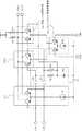
また、図2は図1に示す実施例の具体例を説明する回路である。図2において、11,12,104,105,106及び107は図1と同一符号を付してあり、13,14,21及び22はトランジスタ、15及び23は定電流源、16及び17は容量、18及び19は抵抗、20は定電圧源である。 FIG. 2 is a circuit for explaining a specific example of the embodiment shown in FIG. In FIG. 2, 11, 12, 104, 105, 106 and 107 are assigned the same reference numerals as in FIG. 1, 13, 14, 21 and 22 are transistors, 15 and 23 are constant current sources, and 16 and 17 are capacitors. , 18 and 19 are resistors, and 20 is a constant voltage source.
また、トランジスタ13及び14、定電流源15はトランスコンダクタンスアンプ50を、容量16及び17、抵抗18及び19、定電圧源20はハイパスフィルタ回路51を、トランジスタ21及び22、定電流源23はトランスコンダクタンスアンプ52をそれぞれ構成している。 The
差動入力信号104はトランジスタ13のベース及び容量16の一端にそれぞれ印加され、差動入力信号105はトランジスタ14のベース及び容量17の一端にそれぞれ印加される。また、トランジスタ13のエミッタはトランジスタ14のエミッタ及び定電流源15の一端にそれぞれ接続される。 The
容量16の他端はトランジスタ21のベース及び抵抗18の一端にそれぞれ接続され、容量17の他端はトランジスタ22のベース及び抵抗19の一端にそれぞれ接続される。また、抵抗18の他端は抵抗19の他端及び定電圧源20の一端にそれぞれ接続される。 The other end of the
トランジスタ21のエミッタはトランジスタ22のエミッタ及び定電流源23の一端にそれぞれ接続される。 The emitter of the
さらに、トランジスタ13のコレクタはトランジスタ21のコレクタ及び抵抗11の一端にそれぞれ接続されると共に差動出力信号106として出力され、トランジスタ14のコレクタはトランジスタ22のコレクタ及び抵抗12の一端にそれぞれ接続されると共に差動出力信号107として出力される。 Further, the collector of the
最後に、抵抗11及び12の他端は正電圧源にそれぞれ接続され、定電流源15及び23の他端と、定電圧源20の他端はそれぞれ接地される。 Finally, the other ends of the
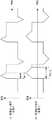
ここで、図1に示す実施例の動作を図2及び図3を用いて説明する。図3は図1に示す実施例の動作を説明するタイミング図である。 The operation of the embodiment shown in FIG. 1 will be described with reference to FIGS. FIG. 3 is a timing chart for explaining the operation of the embodiment shown in FIG.
差動入力信号104及び105は、トランスコンダクタンスアンプ8に入力され差動電流出力として出力され、一方、ハイパスフィルタ回路9に入力された差動入力信号104及び105は、低周波成分が除去された後、トランスコンダクタンスアンプ10に入力され差動電流出力として出力される。 The differential input signals 104 and 105 are input to the transconductance amplifier 8 and output as a differential current output, while the differential input signals 104 and 105 input to the high-pass filter circuit 9 have low frequency components removed. Thereafter, it is input to the transconductance amplifier 10 and output as a differential current output.
すなわち、図2において、差動入力信号104及び105は、トランジスタ13及び14、定電流源15で構成されるトランスコンダクタンスアンプ50に入力され差動電流出力として出力される。 That is, in FIG. 2, differential input signals 104 and 105 are input to a
同様に、図2において、差動入力信号104及び105は、容量16及び17、抵抗18及び19、定電圧源20で構成されるハイパスフィルタ回路51を介してトランジスタ21及び22、定電流源23で構成されるトランスコンダクタンスアンプ52に入力され差動電流出力として出力される。 Similarly, in FIG. 2, differential input signals 104 and 105 are converted into
例えば、図3(a)に示すような差動入力信号がトランスコンダクタンスアンプ8に入力された場合、トランスコンダクタンスアンプ8の差動電流出力は図3(b)に示すようになる。 For example, when a differential input signal as shown in FIG. 3A is input to the transconductance amplifier 8, the differential current output of the transconductance amplifier 8 is as shown in FIG.
一方、例えば、図3(a)に示すような差動入力信号がハイパスフィルタ回路9を介してトランスコンダクタンスアンプ10に入力された場合、トランスコンダクタンスアンプ10の差動電流出力は図3(c)に示すように差動入力信号の立ち上がり、若しくは、立下りの時点でパルス状の出力となる。 On the other hand, for example, when a differential input signal as shown in FIG. 3A is input to the transconductance amplifier 10 via the high-pass filter circuit 9, the differential current output of the transconductance amplifier 10 is as shown in FIG. As shown in FIG. 4, a pulse-like output is obtained when the differential input signal rises or falls.
2つのトランスコンダクタンスアンプ8及び10の差動電流出力は、抵抗11及び12よってそれぞれ加算され電圧変換されて、差動出力信号106及び107として出力される。 The differential current outputs of the two transconductance amplifiers 8 and 10 are added and voltage-converted by the
すなわち、図2において、2つのトランスコンダクタンスアンプ50及び52の差動電流出力は、抵抗11及び12よってそれぞれ加算され電圧変換されて、差動出力信号106及び107として出力される。 That is, in FIG. 2, the differential current outputs of the two
例えば、抵抗11及び12では、図3(b)及び図3(c)に示す差動電流出力がそれぞれ加算されて電圧変換されて出力されるので、差動出力信号は図3(d)に示すようになる。すなわち、差動入力信号の変化点での振幅を大きくしたプリエンファシス信号を得ることができる。 For example, in the
ちなみに、ハイパスフィルタ回路は、従来例で用いられている遅延回路と比較して構成が簡単であるので、チップ面積が大きくなってしまうと言った問題を改善することができる。 Incidentally, the high-pass filter circuit has a simpler configuration than the delay circuit used in the conventional example, so that the problem that the chip area becomes large can be improved.
この結果、差動入力信号を2分割すると共に一方の差動入力信号を第1のトランスコンダクタンスアンプで差動電流出力に変換し、他方の差動入力信号をハイパスフィルタ回路を介して第2のトランスコンダクタンスアンプで差動電流出力に変換し、2つの差動電流出力をそれぞれ加算して電圧変換することにより、簡単な構成でプリエンファシス信号を生成することが可能になる。 As a result, the differential input signal is divided into two, one differential input signal is converted into a differential current output by the first transconductance amplifier, and the other differential input signal is converted to the second through the high-pass filter circuit. It is possible to generate a pre-emphasis signal with a simple configuration by converting to a differential current output by a transconductance amplifier and adding two differential current outputs to perform voltage conversion.
また、図1及び図2に示す実施例では図3中”PE01”に示すようなプリエンファシス強度を変化させることはできない。図4は本発明に係る他の実施例を示す構成ブロック図であり、プリエンファシス強度を変化させることが可能なプリエンファシス回路である。 In the embodiment shown in FIGS. 1 and 2, the pre-emphasis intensity as shown by “PE01” in FIG. 3 cannot be changed. FIG. 4 is a block diagram showing another embodiment of the present invention, which is a pre-emphasis circuit capable of changing the pre-emphasis intensity.
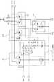
図4において、13,14,15,16,17,18,19,20,21,22,50,51,104及び105は図2と同一符号を付してあり、24及び25は2つのトランスコンダクタンスアンプからの差動電流出力をそれぞれ加算して電圧変換する抵抗、26,27,28及び29はトランジスタ、30は定電流源、106a及び107aは差動出力信号、108及び109はプリエンファシス強度の制御信号である。 4, 13, 14, 15, 16, 17, 18, 19, 20, 21, 22, 50, 51, 104, and 105 are assigned the same reference numerals as in FIG. 2, and 24 and 25 are two transformers. Resistors for adding and converting differential current outputs from conductance amplifiers,
また、トランジスタ21及び22はトランスコンダクタンスアンプ52aを、トランジスタ26及び27は直流レベル調整手段53を、トランジスタ28及び29、定電流源30はプリエンファシス強度調整手段54をそれぞれ構成している。 The
差動入力信号104はトランジスタ13のベース及び容量16の一端にそれぞれ印加され、差動入力信号105はトランジスタ14のベース及び容量17の一端にそれぞれ印加される。また、トランジスタ13のエミッタはトランジスタ14のエミッタ及び定電流源15の一端にそれぞれ接続される。 The
容量16の他端はトランジスタ21のベース及び抵抗18の一端にそれぞれ接続され、容量17の他端はトランジスタ22のベース及び抵抗19の一端にそれぞれ接続される。また、抵抗18の他端は抵抗19の他端、定電圧源20の一端、トランジスタ26及び27のベースにそれぞれ接続される。 The other end of the
トランジスタ21のエミッタはトランジスタ22のエミッタ及びトランジスタ28のコレクタにそれぞれ接続され、トランジスタ26のエミッタはトランジスタ27のエミッタ及びトランジスタ29のコレクタにそれぞれ接続される。また、トランジスタ28のエミッタはトランジスタ29のエミッタ及び定電流源30の一端にそれぞれ接続される。 The emitter of
さらに、トランジスタ13のコレクタはトランジスタ21及び26のコレクタ、抵抗24の一端にそれぞれ接続されると共に差動出力信号106aとして出力され、トランジスタ14のコレクタはトランジスタ22及び27のコレクタ、抵抗25の一端にそれぞれ接続されると共に差動出力信号107aとして出力される。 Further, the collector of the
最後に、抵抗24及び25の他端は正電圧源にそれぞれ接続され、定電流源15及び30の他端と、定電圧源20の他端はそれぞれ接地される。また、トランジスタ28及び29のベースにはプリエンファシス強度の制御信号108及び109がそれぞれ印加される。 Finally, the other ends of the
ここで、図4に示す実施例の動作を説明する。但し、図2に示す実施例と同様の動作に関しては説明を省略する。 Here, the operation of the embodiment shown in FIG. 4 will be described. However, description of operations similar to those in the embodiment shown in FIG. 2 is omitted.
プリエンファシス強度調整手段54において、定電流源30に流れる定電流は、トランジスタ28及び29によってトランスコンダクタンスアンプ52aと直流レベル調整手段53とに分配される。また、直流レベル調整手段53の差動入力端子には定電圧源20の出力電圧がバイアス電圧として印加されている。 In the pre-emphasis intensity adjusting means 54, the constant current flowing through the constant
このため、制御信号108及び109を調整して、トランスコンダクタンスアンプ52aに流れる電流を増加させ、直流レベル調整手段53に流れる電流を減少させることにより、図3中”PE01”に示すプリエンファシス強度を大きくすることができる。 Therefore, by adjusting the control signals 108 and 109, the current flowing through the
一方、制御信号108及び109を調整して、トランスコンダクタンスアンプ52aに流れる電流を減少させ、直流レベル調整手段53に流れる電流を増加させることにより、図3中”PE01”に示すプリエンファシス強度を小さくすることができる。 On the other hand, the control signals 108 and 109 are adjusted to decrease the current flowing through the
プリエンファシス強度を大きくする場合、プリエンファシス強度を小さくする場合、何れの場合であっても、抵抗24および25に供給される電流の和は、トランスコンダクタンスアンプ52aと直流レベル調整手段53とに流れる電流の和、言い換えれば、定電流源30の出力電流となり、直流レベルは変化することはない。 In either case of increasing the pre-emphasis intensity or decreasing the pre-emphasis intensity, the sum of the currents supplied to the
この結果、差動入力信号を2分割して、一方の差動入力信号を第1のトランスコンダクタンスアンプで差動電流出力に変換し、他方の差動入力信号をハイパスフィルタ回路を介して第2のトランスコンダクタンスアンプで差動電流出力に変換し、2つの差動電流出力をそれぞれ加算して電圧変換すると共にプリエンファシス強度調整手段が定電流を第2のトランスコンダクタンスアンプと直流レベル調整手段とに分配することにより、簡単な構成で直流レベルを変化させることなくプリエンファシス強度が可変であるプリエンファシス信号を生成することが可能になる。 As a result, the differential input signal is divided into two, one differential input signal is converted into a differential current output by the first transconductance amplifier, and the other differential input signal is converted to the second through the high-pass filter circuit. Is converted into a differential current output by the transconductance amplifier, and the two differential current outputs are added to each other for voltage conversion, and the pre-emphasis intensity adjusting means converts the constant current to the second transconductance amplifier and the DC level adjusting means. By distributing, it is possible to generate a pre-emphasis signal with a variable pre-emphasis intensity without changing the DC level with a simple configuration.
また、図5は本発明に係る他の実施例を示す構成ブロック図であり、プリエンファシス時間(プリエンファシスされている時間)を変化させることが可能なプリエンファシス回路である。 FIG. 5 is a block diagram showing the configuration of another embodiment according to the present invention, which is a pre-emphasis circuit capable of changing the pre-emphasis time (pre-emphasis time).
図5において、13,14,15,16,17,18,19,20,21,22,24,25,26,27,28,29,30,50,52a,53,54,104,105,108及び109は図4と同一符号を付してあり、31及び32はスイッチ回路、33及び34は容量、106b及び107bは差動出力信号である。 In FIG. 5, 13, 14, 15, 16, 17, 18, 19, 20, 21, 22, 24, 25, 26, 27, 28, 29, 30, 50, 52a, 53, 54, 104, 105,
また、容量16,17,33及び34、抵抗18及び19、定電圧源20、並びに、スイッチ回路31及び32は周波数特性(カットオフ周波数)が可変なハイパスフィルタ回路55を構成している。 The
ここで、図5に示す実施例の動作を図6を用いて説明する。図6は図5に示す実施例の動作を説明するタイミング図である。但し、図2、或いは、図4に示す実施例と同様の動作に関しては説明を省略する。 Here, the operation of the embodiment shown in FIG. 5 will be described with reference to FIG. FIG. 6 is a timing chart for explaining the operation of the embodiment shown in FIG. However, the description of the same operation as that of the embodiment shown in FIG. 2 or FIG. 4 is omitted.
スイッチ回路31及び32は図示しない制御信号によって”ON/OFF”を制御され、スイッチ回路31及び32が”OFF”の場合、ハイパスフィルタ回路55は、容量16と抵抗18、並びに、容量17と抵抗19によって個々のハイパスフィルタが構成される。 The
一方、スイッチ回路31及び32が”ON”の場合、ハイパスフィルタ回路55は、容量16及び容量33の並列回路と抵抗18、並びに、容量17及び容量34の並列回路と抵抗19によって個々のハイパスフィルタが構成されることになる。 On the other hand, when the
スイッチ回路31及び32が”ON”の場合は、スイッチ回路31及び32が”OFF”の場合と比較して容量が大きくなり、周波数特性(カットオフ周波数)が変化してプリエンファシス時間を長くすることができる。 When the
例えば、図6(a)はスイッチ回路31及び32が”OFF”の場合(容量小)の差動出力信号を示し、また、図6(b)はスイッチ回路31及び32が”ON”の場合(容量大)の差動出力信号を示している。 For example, FIG. 6A shows the differential output signal when the
図6中”PE12”に示すプリエンファシス時間は、図6中”PE11”に示すプリエンファシス時間と比較して長くなり、言い換えれば、周波数特性(カットオフ周波数)が可変なハイパスフィルタ回路55を用いることにより。プリエンファシス時間が可変になる。 The pre-emphasis time indicated by “PE12” in FIG. 6 is longer than the pre-emphasis time indicated by “PE11” in FIG. 6, in other words, the high-pass filter circuit 55 having a variable frequency characteristic (cutoff frequency) is used. By Pre-emphasis time is variable.
この結果、差動入力信号を2分割して、一方の差動入力信号を第1のトランスコンダクタンスアンプで差動電流出力に変換し、他方の差動入力信号をハイパスフィルタ回路を介して第2のトランスコンダクタンスアンプで差動電流出力に変換し、2つの差動電流出力をそれぞれ加算して電圧変換すると共に周波数特性(カットオフ周波数)が可変なハイパスフィルタ回路を用いることにより、プリエンファシス時間が可変であるプリエンファシス信号を生成することが可能になる。 As a result, the differential input signal is divided into two, one differential input signal is converted into a differential current output by the first transconductance amplifier, and the other differential input signal is converted to the second through the high-pass filter circuit. The pre-emphasis time is converted into a differential current output by a transconductance amplifier, and the two differential current outputs are summed and converted into a voltage, and a high-pass filter circuit having a variable frequency characteristic (cut-off frequency) is used. It is possible to generate a pre-emphasis signal that is variable.
なお、図1等に示す実施例の説明に際しては、具体例としてトランジスタ(正確には、バイポーラトランジスタ)を用いているが、勿論、MOS(Metal Oxide Semiconductor)トランジスタを用いて構成しても構わない。 In the description of the embodiment shown in FIG. 1 and the like, a transistor (precisely, a bipolar transistor) is used as a specific example, but of course, a MOS (Metal Oxide Semiconductor) transistor may be used. .
また、図4及び図5に示す実施例のプリエンファシス強度調整手段54では、ベースにそれぞれ制御信号が印加されエミッタが相互に接続されそれぞれのコレクタから第2のトランスコンダクタンスアンプと直流レベル調整手段とに電流を出力する2つのトランジスタと、これらトランジスタのエミッタに接続された定電流源から構成されているが、リニアリティ向上のために、2つのトランジスタのエミッタと定電流源の一端の間に抵抗をそれぞれ設けても構わない。 In the pre-emphasis intensity adjusting means 54 of the embodiment shown in FIGS. 4 and 5, the control signal is applied to the bases, the emitters are connected to each other, and the second transconductance amplifier and the DC level adjusting means are connected to each collector. In order to improve linearity, a resistor is connected between the emitter of the two transistors and one end of the constant current source. Each may be provided.
また、同様に、2つのトランジスタのエミッタ間に抵抗を設けると共に、2つのトランジスタのエミッタに一端がそれぞれ接続される2つの定電流源を設ける構成であっても構わない。 Similarly, a configuration in which a resistor is provided between the emitters of the two transistors and two constant current sources each having one end connected to the emitters of the two transistors may be provided.
また、図5に示す実施例では、図4の実施例に周波数特性(カットオフ周波数)が可変なハイパスフィルタ回路を適用しているが、図2に示す実施例(プリエンファシス強度が固定のプリエンファシス回路)に周波数特性(カットオフ周波数)が可変なハイパスフィルタ回路を適用しても勿論構わない。 In the embodiment shown in FIG. 5, the high-pass filter circuit having a variable frequency characteristic (cut-off frequency) is applied to the embodiment shown in FIG. 4, but the embodiment shown in FIG. 2 (the pre-emphasis intensity is fixed). Of course, a high-pass filter circuit having a variable frequency characteristic (cut-off frequency) may be applied to the emphasis circuit.
また、図5に示す実施例では、ハイパスフィルタ回路を構成する2つの容量16及び17のそれぞれに対してスイッチ回路によって1つの容量を並列に接続/非接続する構成となっているが、スイッチ回路によって並列に接続/非接続される容量の数は、勿論、2以上であっても構わない。 In the embodiment shown in FIG. 5, one capacitor is connected / disconnected in parallel by the switch circuit to each of the two
1 送信器
2 受信器
3 伝送線路
4,6 ドライバ回路
5 遅延回路
7 減算回路
8,10,50,52,52a トランスコンダクタンスアンプ
9,51,55 ハイパスフィルタ回路
11,12,18,19,24,25 抵抗
13,14,21,22,26,27,28,29 トランジスタ
15,23,30 定電流源
16,17,33,34 容量
20 定電圧源
31,32 スイッチ回路
53 直流レベル調整手段
54 プリエンファシス強度調整手段
100,101,104,105 差動入力信号
102,103,106,106a,106b,107,107a,107b 差動出力信号
108,109 制御信号DESCRIPTION OF SYMBOLS 1 Transmitter 2 Receiver 3 Transmission line 4,6 Driver circuit 5 Delay circuit 7
Claims (10)
Translated fromJapanese差動入力信号を差動電流出力に変換する第1のトランスコンダクタンスアンプと、
ハイパスフィルタ回路と、
このハイパスフィルタ回路を介した前記差動入力信号を差動電流出力に変換する第2のトランスコンダクタンスアンプと、
2つの前記差動電流出力をそれぞれ加算して電圧変換する第1及び第2の抵抗と
を備えたことを特徴とするプリエンファシス回路。In the pre-emphasis circuit that increases the amplitude at the signal change point,
A first transconductance amplifier that converts a differential input signal to a differential current output;
A high-pass filter circuit;
A second transconductance amplifier that converts the differential input signal through the high-pass filter circuit into a differential current output;
A pre-emphasis circuit comprising a first resistor and a second resistor for adding two differential current outputs to perform voltage conversion.
エミッタが相互に接続されそれぞれのコレクタから前記差動電流出力を出力する2つのトランジスタと、
これらトランジスタのエミッタに接続された定電流源から構成されたことを特徴とする
請求項1記載のプリエンファシス回路。The transconductance amplifier is
Two transistors having emitters connected to each other and outputting the differential current output from respective collectors;
2. A pre-emphasis circuit according to claim 1, comprising a constant current source connected to the emitters of these transistors.
差動入力信号を差動電流出力に変換する第1のトランスコンダクタンスアンプと、
ハイパスフィルタ回路と、
このハイパスフィルタ回路を介した前記差動入力信号を差動電流出力に変換する第2のトランスコンダクタンスアンプと、
2つの前記差動電流出力をそれぞれ加算して電圧変換する第1及び第2の抵抗と、
前記第1及び第2の抵抗に出力電流を出力する直流レベル調整手段と、
前記第2のトランスコンダクタンスアンプと前記直流レベル調整手段とに定電流を分配して供給するプリエンファシス強度調整手段と
を備えたことを特徴とするプリエンファシス回路。In the pre-emphasis circuit that increases the amplitude at the signal change point,
A first transconductance amplifier that converts a differential input signal to a differential current output;
A high-pass filter circuit;
A second transconductance amplifier that converts the differential input signal through the high-pass filter circuit into a differential current output;
First and second resistors for adding and converting the two differential current outputs, respectively,
DC level adjusting means for outputting an output current to the first and second resistors;
A pre-emphasis circuit comprising pre-emphasis intensity adjusting means for distributing and supplying a constant current to the second transconductance amplifier and the DC level adjusting means.
エミッタが相互に接続されそれぞれのコレクタから前記差動電流出力を出力する2つのトランジスタと、
これらトランジスタのエミッタに接続された定電流源から構成されたことを特徴とする
請求項3記載のプリエンファシス回路。The first transconductance amplifier is
Two transistors having emitters connected to each other and outputting the differential current output from respective collectors;
4. The pre-emphasis circuit according to claim 3, comprising a constant current source connected to the emitters of these transistors.
エミッタが相互に接続されそれぞれのコレクタから前記差動電流出力を出力する2つのトランジスタとから構成されたことを特徴とする
請求項3記載のプリエンファシス回路。The second transconductance amplifier is
4. The pre-emphasis circuit according to claim 3, wherein the pre-emphasis circuit is composed of two transistors that are connected to each other and that output the differential current output from each collector.
ベースにバイアス電圧が印加されエミッタが相互に接続されそれぞれのコレクタから前記第1及び第2の抵抗に出力電流を出力する2つのトランジスタとから構成されたことを特徴とする
請求項3記載のプリエンファシス回路。The DC level adjusting means is
4. A pre-transistor according to claim 3, wherein a bias voltage is applied to the base, emitters are connected to each other, and two transistors output output currents from the respective collectors to the first and second resistors. Emphasis circuit.
ベースにそれぞれ制御信号が印加されエミッタが相互に接続されそれぞれのコレクタから前記第2のトランスコンダクタンスアンプと前記直流レベル調整手段とに電流を出力する2つのトランジスタと、
これらトランジスタのエミッタに接続された定電流源から構成されたことを特徴とする
請求項3記載のプリエンファシス回路。The pre-emphasis intensity adjusting means is
Two transistors each having a control signal applied to a base and emitters connected to each other and outputting current from the respective collectors to the second transconductance amplifier and the DC level adjusting means;
4. The pre-emphasis circuit according to claim 3, comprising a constant current source connected to the emitters of these transistors.
前記差動入力信号がそれぞれ一端に接続される2つの容量と、
これら容量の他端がそれぞれ一端に接続される2つの抵抗と、
これら抵抗の他端の両方が一端に接続される定電圧源とから構成されたことを特徴とする
請求項1若しくは請求項3記載のプリエンファシス回路。The high-pass filter circuit is
Two capacitors each connected to one end of the differential input signal;
Two resistors each having the other end of the capacitor connected to one end;
4. The pre-emphasis circuit according to claim 1, wherein both of the other ends of the resistors are constituted by a constant voltage source connected to one end.
周波数特性が可変なハイパスフィルタ回路であることを特徴とする
請求項1若しくは請求項3記載のプリエンファシス回路。The high-pass filter circuit is
4. The pre-emphasis circuit according to claim 1, wherein the pre-emphasis circuit is a high-pass filter circuit having variable frequency characteristics.
前記差動入力信号がそれぞれ一端に接続される2つの容量と、
これら容量の他端がそれぞれ一端に接続される2つの抵抗と、
これら抵抗の他端の両方が一端に接続される定電圧源と、
前記2つの容量のそれぞれに設けられスイッチ回路によって並列に接続/非接続される1つ以上の容量とから構成されたことを特徴とする
請求項9記載のプリエンファシス回路。The high-pass filter circuit is
Two capacitors each connected to one end of the differential input signal;
Two resistors each having the other end of the capacitor connected to one end;
A constant voltage source in which both ends of these resistors are connected to one end;
The pre-emphasis circuit according to claim 9, wherein the pre-emphasis circuit includes one or more capacitors provided in each of the two capacitors and connected / disconnected in parallel by a switch circuit.
Priority Applications (1)
| Application Number | Priority Date | Filing Date | Title |
|---|---|---|---|
| JP2007320771AJP5098617B2 (en) | 2007-12-12 | 2007-12-12 | Pre-emphasis circuit |
Applications Claiming Priority (1)
| Application Number | Priority Date | Filing Date | Title |
|---|---|---|---|
| JP2007320771AJP5098617B2 (en) | 2007-12-12 | 2007-12-12 | Pre-emphasis circuit |
Publications (2)
| Publication Number | Publication Date |
|---|---|
| JP2009147512Atrue JP2009147512A (en) | 2009-07-02 |
| JP5098617B2 JP5098617B2 (en) | 2012-12-12 |
Family
ID=40917650
Family Applications (1)
| Application Number | Title | Priority Date | Filing Date |
|---|---|---|---|
| JP2007320771AExpired - Fee RelatedJP5098617B2 (en) | 2007-12-12 | 2007-12-12 | Pre-emphasis circuit |
Country Status (1)
| Country | Link |
|---|---|
| JP (1) | JP5098617B2 (en) |
Cited By (15)
| Publication number | Priority date | Publication date | Assignee | Title |
|---|---|---|---|---|
| JP2010056620A (en)* | 2008-08-26 | 2010-03-11 | Ricoh Co Ltd | Driver circuit |
| JP2012104953A (en)* | 2010-11-08 | 2012-05-31 | Fujitsu Ltd | Emphasis signal generation circuit and signal synthesis circuit |
| JP2012161077A (en)* | 2011-01-28 | 2012-08-23 | Silicon Works Co Ltd | Pre-emphasis circuit and differential current signal transmission system |
| JP2012204948A (en)* | 2011-03-24 | 2012-10-22 | Kawasaki Microelectronics Inc | Differential output buffer |
| US8710918B2 (en) | 2011-08-30 | 2014-04-29 | Fujitsu Limited | Electronic component and reflected-wave cancelling method |
| JP2014090317A (en)* | 2012-10-30 | 2014-05-15 | Fujitsu Ltd | Light-emitting element driving circuit and light-emitting device |
| JP2015019352A (en)* | 2013-07-12 | 2015-01-29 | 富士通株式会社 | Transmitter, circuit and method having high frequency amplification |
| JP2015065687A (en)* | 2014-11-26 | 2015-04-09 | 富士通株式会社 | Signal shaping circuit |
| JP2015139039A (en)* | 2014-01-21 | 2015-07-30 | 富士通株式会社 | Emphasis signal generation circuit |
| JP2016040896A (en)* | 2014-08-13 | 2016-03-24 | 日本電信電話株式会社 | Pre-emphasis circuit and output buffer circuit |
| JP5971366B1 (en)* | 2015-02-27 | 2016-08-17 | 沖電気工業株式会社 | driver |
| JP2016534599A (en)* | 2013-10-25 | 2016-11-04 | 華為技術有限公司Huawei Technologies Co.,Ltd. | Copper wire interface circuit |
| US9722545B2 (en) | 2013-03-04 | 2017-08-01 | Mitsubishi Electric Corporation | Emphasis circuit |
| JP2018532295A (en)* | 2015-08-25 | 2018-11-01 | クアルコム,インコーポレイテッド | Low noise amplifier and notch filter |
| JP2018198261A (en)* | 2017-05-24 | 2018-12-13 | 富士通株式会社 | Light-emitting element drive circuit, optical module, and active optical cable |
Citations (12)
| Publication number | Priority date | Publication date | Assignee | Title |
|---|---|---|---|---|
| JPH0630378A (en)* | 1992-07-08 | 1994-02-04 | Toshiba Corp | White clip / dark clip circuit |
| JPH06152340A (en)* | 1992-10-29 | 1994-05-31 | Fujitsu Ltd | Line equalizing circuit |
| JPH0766708A (en)* | 1993-08-30 | 1995-03-10 | Fujitsu Ltd | Input buffer gate |
| JP2004088693A (en)* | 2002-08-29 | 2004-03-18 | Toshiba Corp | Differential data driver circuit |
| JP2004357004A (en)* | 2003-05-29 | 2004-12-16 | Nec Electronics Corp | Transmitter circuit, transmission circuit and driving device |
| JP2005217999A (en)* | 2004-02-02 | 2005-08-11 | Hitachi Ltd | Digital data transmission circuit |
| JP2005229595A (en)* | 2004-01-26 | 2005-08-25 | Lg Electronics Inc | Emphasis circuit |
| JP2007505575A (en)* | 2003-09-11 | 2007-03-08 | ザイリンクス インコーポレイテッド | DAC-based line driver with selectable pre-emphasis signal level |
| JP2007060073A (en)* | 2005-08-23 | 2007-03-08 | Nec Electronics Corp | Output buffer circuit having de-emphasis function |
| JP2007081608A (en)* | 2005-09-13 | 2007-03-29 | Nec Electronics Corp | Output buffer circuit |
| JP2007129619A (en)* | 2005-11-07 | 2007-05-24 | National Institute Of Advanced Industrial & Technology | Equalizer circuit |
| JP2007158557A (en)* | 2005-12-02 | 2007-06-21 | Yokogawa Electric Corp | Self-excited oscillation circuit |
- 2007
- 2007-12-12JPJP2007320771Apatent/JP5098617B2/ennot_activeExpired - Fee Related
Patent Citations (12)
| Publication number | Priority date | Publication date | Assignee | Title |
|---|---|---|---|---|
| JPH0630378A (en)* | 1992-07-08 | 1994-02-04 | Toshiba Corp | White clip / dark clip circuit |
| JPH06152340A (en)* | 1992-10-29 | 1994-05-31 | Fujitsu Ltd | Line equalizing circuit |
| JPH0766708A (en)* | 1993-08-30 | 1995-03-10 | Fujitsu Ltd | Input buffer gate |
| JP2004088693A (en)* | 2002-08-29 | 2004-03-18 | Toshiba Corp | Differential data driver circuit |
| JP2004357004A (en)* | 2003-05-29 | 2004-12-16 | Nec Electronics Corp | Transmitter circuit, transmission circuit and driving device |
| JP2007505575A (en)* | 2003-09-11 | 2007-03-08 | ザイリンクス インコーポレイテッド | DAC-based line driver with selectable pre-emphasis signal level |
| JP2005229595A (en)* | 2004-01-26 | 2005-08-25 | Lg Electronics Inc | Emphasis circuit |
| JP2005217999A (en)* | 2004-02-02 | 2005-08-11 | Hitachi Ltd | Digital data transmission circuit |
| JP2007060073A (en)* | 2005-08-23 | 2007-03-08 | Nec Electronics Corp | Output buffer circuit having de-emphasis function |
| JP2007081608A (en)* | 2005-09-13 | 2007-03-29 | Nec Electronics Corp | Output buffer circuit |
| JP2007129619A (en)* | 2005-11-07 | 2007-05-24 | National Institute Of Advanced Industrial & Technology | Equalizer circuit |
| JP2007158557A (en)* | 2005-12-02 | 2007-06-21 | Yokogawa Electric Corp | Self-excited oscillation circuit |
Cited By (17)
| Publication number | Priority date | Publication date | Assignee | Title |
|---|---|---|---|---|
| JP2010056620A (en)* | 2008-08-26 | 2010-03-11 | Ricoh Co Ltd | Driver circuit |
| JP2012104953A (en)* | 2010-11-08 | 2012-05-31 | Fujitsu Ltd | Emphasis signal generation circuit and signal synthesis circuit |
| JP2012161077A (en)* | 2011-01-28 | 2012-08-23 | Silicon Works Co Ltd | Pre-emphasis circuit and differential current signal transmission system |
| JP2012204948A (en)* | 2011-03-24 | 2012-10-22 | Kawasaki Microelectronics Inc | Differential output buffer |
| US8710918B2 (en) | 2011-08-30 | 2014-04-29 | Fujitsu Limited | Electronic component and reflected-wave cancelling method |
| JP2014090317A (en)* | 2012-10-30 | 2014-05-15 | Fujitsu Ltd | Light-emitting element driving circuit and light-emitting device |
| US9722545B2 (en) | 2013-03-04 | 2017-08-01 | Mitsubishi Electric Corporation | Emphasis circuit |
| JP2015019352A (en)* | 2013-07-12 | 2015-01-29 | 富士通株式会社 | Transmitter, circuit and method having high frequency amplification |
| JP2016534599A (en)* | 2013-10-25 | 2016-11-04 | 華為技術有限公司Huawei Technologies Co.,Ltd. | Copper wire interface circuit |
| US9742463B2 (en) | 2013-10-25 | 2017-08-22 | Huawei Technologies Co., Ltd. | Copper wire interface circuit |
| KR101897526B1 (en)* | 2013-10-25 | 2018-10-31 | 후아웨이 테크놀러지 컴퍼니 리미티드 | Copper wire interface circuit |
| JP2015139039A (en)* | 2014-01-21 | 2015-07-30 | 富士通株式会社 | Emphasis signal generation circuit |
| JP2016040896A (en)* | 2014-08-13 | 2016-03-24 | 日本電信電話株式会社 | Pre-emphasis circuit and output buffer circuit |
| JP2015065687A (en)* | 2014-11-26 | 2015-04-09 | 富士通株式会社 | Signal shaping circuit |
| JP5971366B1 (en)* | 2015-02-27 | 2016-08-17 | 沖電気工業株式会社 | driver |
| JP2018532295A (en)* | 2015-08-25 | 2018-11-01 | クアルコム,インコーポレイテッド | Low noise amplifier and notch filter |
| JP2018198261A (en)* | 2017-05-24 | 2018-12-13 | 富士通株式会社 | Light-emitting element drive circuit, optical module, and active optical cable |
Also Published As
| Publication number | Publication date |
|---|---|
| JP5098617B2 (en) | 2012-12-12 |
Similar Documents
| Publication | Publication Date | Title |
|---|---|---|
| JP5098617B2 (en) | Pre-emphasis circuit | |
| EP0766381B1 (en) | Improved single-ended to differential converter with relaxed common-mode input requirements | |
| JP4664835B2 (en) | Regulator structure with variable amplifier | |
| WO2017014262A1 (en) | Analog multiplexer core circuit and analog multiplexer circuit | |
| US12149219B2 (en) | Transconductor circuitry with adaptive biasing | |
| US7696822B2 (en) | Amplifying circuit and associated linearity improving method | |
| JP2019041155A (en) | OTA circuit and filter | |
| JP4763662B2 (en) | Transimpedance amplifier | |
| US6972624B1 (en) | Low-voltage high dynamic range variable-gain amplifier | |
| US7477103B2 (en) | Amplifier circuit | |
| JP2010220195A (en) | Current conveyor based instrumentation amplifier | |
| US8680919B2 (en) | Impedance adjustments in amplifiers | |
| JP5238604B2 (en) | Voltage conversion circuit and wireless communication device | |
| CN101171745B (en) | Receiver having a gain-controllable input amplifier | |
| US20160181997A1 (en) | Signal amplifying circuit | |
| US10003304B2 (en) | Operational amplifier and method for reducing offset voltage of operational amplifier | |
| CN101453195A (en) | Method for improving common mode feedback stability by using grounding capacitor | |
| JP4613495B2 (en) | Preamplifier | |
| JP4571145B2 (en) | Transconductance circuit | |
| JP5007937B2 (en) | Attenuator | |
| CN112865730B (en) | Class-D amplifier circuit and audio amplification method | |
| JP4721928B2 (en) | Variable transconductor | |
| CN218499143U (en) | Inverting circuit, modulation circuit, modulator, transmitting device and communication system | |
| US20050063477A1 (en) | Transmitter/receiver for bidirectional communications | |
| WO2011027387A1 (en) | Amplifier |
Legal Events
| Date | Code | Title | Description |
|---|---|---|---|
| A621 | Written request for application examination | Free format text:JAPANESE INTERMEDIATE CODE: A621 Effective date:20100924 | |
| A977 | Report on retrieval | Free format text:JAPANESE INTERMEDIATE CODE: A971007 Effective date:20120622 | |
| A131 | Notification of reasons for refusal | Free format text:JAPANESE INTERMEDIATE CODE: A131 Effective date:20120628 | |
| A521 | Written amendment | Free format text:JAPANESE INTERMEDIATE CODE: A523 Effective date:20120808 | |
| TRDD | Decision of grant or rejection written | ||
| A01 | Written decision to grant a patent or to grant a registration (utility model) | Free format text:JAPANESE INTERMEDIATE CODE: A01 Effective date:20120828 | |
| A01 | Written decision to grant a patent or to grant a registration (utility model) | Free format text:JAPANESE INTERMEDIATE CODE: A01 | |
| A61 | First payment of annual fees (during grant procedure) | Free format text:JAPANESE INTERMEDIATE CODE: A61 Effective date:20120910 | |
| FPAY | Renewal fee payment (event date is renewal date of database) | Free format text:PAYMENT UNTIL: 20151005 Year of fee payment:3 | |
| R150 | Certificate of patent or registration of utility model | Free format text:JAPANESE INTERMEDIATE CODE: R150 | |
| LAPS | Cancellation because of no payment of annual fees |