JP2009145500A - Video display apparatus and method for driving the same - Google Patents
Video display apparatus and method for driving the sameDownload PDFInfo
- Publication number
- JP2009145500A JP2009145500AJP2007321212AJP2007321212AJP2009145500AJP 2009145500 AJP2009145500 AJP 2009145500AJP 2007321212 AJP2007321212 AJP 2007321212AJP 2007321212 AJP2007321212 AJP 2007321212AJP 2009145500 AJP2009145500 AJP 2009145500A
- Authority
- JP
- Japan
- Prior art keywords
- liquid crystal
- crystal display
- correction value
- display element
- electrode
- Prior art date
- Legal status (The legal status is an assumption and is not a legal conclusion. Google has not performed a legal analysis and makes no representation as to the accuracy of the status listed.)
- Pending
Links
- 238000000034methodMethods0.000titleclaimsdescription12
- 239000004973liquid crystal related substanceSubstances0.000claimsabstractdescription128
- 239000011159matrix materialSubstances0.000claimsabstractdescription12
- 239000000758substrateSubstances0.000claimsdescription69
- 238000000926separation methodMethods0.000claimsdescription24
- 230000007274generation of a signal involved in cell-cell signalingEffects0.000claimsdescription3
- 230000015556catabolic processEffects0.000abstractdescription4
- 238000006731degradation reactionMethods0.000abstractdescription4
- 235000019557luminanceNutrition0.000description16
- 239000010408filmSubstances0.000description9
- 239000003990capacitorSubstances0.000description6
- 238000001514detection methodMethods0.000description5
- 238000010586diagramMethods0.000description4
- 230000002159abnormal effectEffects0.000description3
- 239000003086colorantSubstances0.000description3
- 230000007423decreaseEffects0.000description3
- 230000006866deteriorationEffects0.000description3
- 230000010287polarizationEffects0.000description3
- 239000011521glassSubstances0.000description2
- 229910010272inorganic materialInorganic materials0.000description2
- 239000011147inorganic materialSubstances0.000description2
- 230000003287optical effectEffects0.000description2
- 230000003071parasitic effectEffects0.000description2
- 239000004033plasticSubstances0.000description2
- 239000010453quartzSubstances0.000description2
- VYPSYNLAJGMNEJ-UHFFFAOYSA-Nsilicon dioxideInorganic materialsO=[Si]=OVYPSYNLAJGMNEJ-UHFFFAOYSA-N0.000description2
- 239000012780transparent materialSubstances0.000description2
- 241000255777LepidopteraSpecies0.000description1
- 230000005684electric fieldEffects0.000description1
- 229910052736halogenInorganic materials0.000description1
- 150000002367halogensChemical class0.000description1
- AMGQUBHHOARCQH-UHFFFAOYSA-Nindium;oxotinChemical compound[In].[Sn]=OAMGQUBHHOARCQH-UHFFFAOYSA-N0.000description1
- QSHDDOUJBYECFT-UHFFFAOYSA-NmercuryChemical compound[Hg]QSHDDOUJBYECFT-UHFFFAOYSA-N0.000description1
- 229910052753mercuryInorganic materials0.000description1
- 229910001507metal halideInorganic materials0.000description1
- 150000005309metal halidesChemical class0.000description1
- 239000003566sealing materialSubstances0.000description1
- 239000010409thin filmSubstances0.000description1
- 238000002834transmittanceMethods0.000description1
- 229910052724xenonInorganic materials0.000description1
- FHNFHKCVQCLJFQ-UHFFFAOYSA-Nxenon atomChemical compound[Xe]FHNFHKCVQCLJFQ-UHFFFAOYSA-N0.000description1
Images


Classifications
- H—ELECTRICITY
- H04—ELECTRIC COMMUNICATION TECHNIQUE
- H04N—PICTORIAL COMMUNICATION, e.g. TELEVISION
- H04N9/00—Details of colour television systems
- H04N9/12—Picture reproducers
- H04N9/31—Projection devices for colour picture display, e.g. using electronic spatial light modulators [ESLM]
- H04N9/3102—Projection devices for colour picture display, e.g. using electronic spatial light modulators [ESLM] using two-dimensional electronic spatial light modulators
- H04N9/3105—Projection devices for colour picture display, e.g. using electronic spatial light modulators [ESLM] using two-dimensional electronic spatial light modulators for displaying all colours simultaneously, e.g. by using two or more electronic spatial light modulators
- H04N9/3108—Projection devices for colour picture display, e.g. using electronic spatial light modulators [ESLM] using two-dimensional electronic spatial light modulators for displaying all colours simultaneously, e.g. by using two or more electronic spatial light modulators by using a single electronic spatial light modulator
- G—PHYSICS
- G09—EDUCATION; CRYPTOGRAPHY; DISPLAY; ADVERTISING; SEALS
- G09G—ARRANGEMENTS OR CIRCUITS FOR CONTROL OF INDICATING DEVICES USING STATIC MEANS TO PRESENT VARIABLE INFORMATION
- G09G3/00—Control arrangements or circuits, of interest only in connection with visual indicators other than cathode-ray tubes
- G09G3/20—Control arrangements or circuits, of interest only in connection with visual indicators other than cathode-ray tubes for presentation of an assembly of a number of characters, e.g. a page, by composing the assembly by combination of individual elements arranged in a matrix no fixed position being assigned to or needed to be assigned to the individual characters or partial characters
- G09G3/34—Control arrangements or circuits, of interest only in connection with visual indicators other than cathode-ray tubes for presentation of an assembly of a number of characters, e.g. a page, by composing the assembly by combination of individual elements arranged in a matrix no fixed position being assigned to or needed to be assigned to the individual characters or partial characters by control of light from an independent source
- G09G3/36—Control arrangements or circuits, of interest only in connection with visual indicators other than cathode-ray tubes for presentation of an assembly of a number of characters, e.g. a page, by composing the assembly by combination of individual elements arranged in a matrix no fixed position being assigned to or needed to be assigned to the individual characters or partial characters by control of light from an independent source using liquid crystals
- G—PHYSICS
- G02—OPTICS
- G02F—OPTICAL DEVICES OR ARRANGEMENTS FOR THE CONTROL OF LIGHT BY MODIFICATION OF THE OPTICAL PROPERTIES OF THE MEDIA OF THE ELEMENTS INVOLVED THEREIN; NON-LINEAR OPTICS; FREQUENCY-CHANGING OF LIGHT; OPTICAL LOGIC ELEMENTS; OPTICAL ANALOGUE/DIGITAL CONVERTERS
- G02F1/00—Devices or arrangements for the control of the intensity, colour, phase, polarisation or direction of light arriving from an independent light source, e.g. switching, gating or modulating; Non-linear optics
- G02F1/01—Devices or arrangements for the control of the intensity, colour, phase, polarisation or direction of light arriving from an independent light source, e.g. switching, gating or modulating; Non-linear optics for the control of the intensity, phase, polarisation or colour
- G02F1/13—Devices or arrangements for the control of the intensity, colour, phase, polarisation or direction of light arriving from an independent light source, e.g. switching, gating or modulating; Non-linear optics for the control of the intensity, phase, polarisation or colour based on liquid crystals, e.g. single liquid crystal display cells
- G02F1/133—Constructional arrangements; Operation of liquid crystal cells; Circuit arrangements
- G—PHYSICS
- G09—EDUCATION; CRYPTOGRAPHY; DISPLAY; ADVERTISING; SEALS
- G09G—ARRANGEMENTS OR CIRCUITS FOR CONTROL OF INDICATING DEVICES USING STATIC MEANS TO PRESENT VARIABLE INFORMATION
- G09G3/00—Control arrangements or circuits, of interest only in connection with visual indicators other than cathode-ray tubes
- G09G3/20—Control arrangements or circuits, of interest only in connection with visual indicators other than cathode-ray tubes for presentation of an assembly of a number of characters, e.g. a page, by composing the assembly by combination of individual elements arranged in a matrix no fixed position being assigned to or needed to be assigned to the individual characters or partial characters
- G09G3/34—Control arrangements or circuits, of interest only in connection with visual indicators other than cathode-ray tubes for presentation of an assembly of a number of characters, e.g. a page, by composing the assembly by combination of individual elements arranged in a matrix no fixed position being assigned to or needed to be assigned to the individual characters or partial characters by control of light from an independent source
- G09G3/36—Control arrangements or circuits, of interest only in connection with visual indicators other than cathode-ray tubes for presentation of an assembly of a number of characters, e.g. a page, by composing the assembly by combination of individual elements arranged in a matrix no fixed position being assigned to or needed to be assigned to the individual characters or partial characters by control of light from an independent source using liquid crystals
- G09G3/3611—Control of matrices with row and column drivers
- G09G3/3648—Control of matrices with row and column drivers using an active matrix
- G—PHYSICS
- G09—EDUCATION; CRYPTOGRAPHY; DISPLAY; ADVERTISING; SEALS
- G09G—ARRANGEMENTS OR CIRCUITS FOR CONTROL OF INDICATING DEVICES USING STATIC MEANS TO PRESENT VARIABLE INFORMATION
- G09G5/00—Control arrangements or circuits for visual indicators common to cathode-ray tube indicators and other visual indicators
- G09G5/10—Intensity circuits
- G—PHYSICS
- G09—EDUCATION; CRYPTOGRAPHY; DISPLAY; ADVERTISING; SEALS
- G09G—ARRANGEMENTS OR CIRCUITS FOR CONTROL OF INDICATING DEVICES USING STATIC MEANS TO PRESENT VARIABLE INFORMATION
- G09G2320/00—Control of display operating conditions
- G09G2320/02—Improving the quality of display appearance
- G09G2320/0204—Compensation of DC component across the pixels in flat panels
- G—PHYSICS
- G09—EDUCATION; CRYPTOGRAPHY; DISPLAY; ADVERTISING; SEALS
- G09G—ARRANGEMENTS OR CIRCUITS FOR CONTROL OF INDICATING DEVICES USING STATIC MEANS TO PRESENT VARIABLE INFORMATION
- G09G2320/00—Control of display operating conditions
- G09G2320/02—Improving the quality of display appearance
- G09G2320/0209—Crosstalk reduction, i.e. to reduce direct or indirect influences of signals directed to a certain pixel of the displayed image on other pixels of said image, inclusive of influences affecting pixels in different frames or fields or sub-images which constitute a same image, e.g. left and right images of a stereoscopic display
- G09G2320/0214—Crosstalk reduction, i.e. to reduce direct or indirect influences of signals directed to a certain pixel of the displayed image on other pixels of said image, inclusive of influences affecting pixels in different frames or fields or sub-images which constitute a same image, e.g. left and right images of a stereoscopic display with crosstalk due to leakage current of pixel switch in active matrix panels
- G—PHYSICS
- G09—EDUCATION; CRYPTOGRAPHY; DISPLAY; ADVERTISING; SEALS
- G09G—ARRANGEMENTS OR CIRCUITS FOR CONTROL OF INDICATING DEVICES USING STATIC MEANS TO PRESENT VARIABLE INFORMATION
- G09G2320/00—Control of display operating conditions
- G09G2320/02—Improving the quality of display appearance
- G09G2320/0219—Reducing feedthrough effects in active matrix panels, i.e. voltage changes on the scan electrode influencing the pixel voltage due to capacitive coupling
- G—PHYSICS
- G09—EDUCATION; CRYPTOGRAPHY; DISPLAY; ADVERTISING; SEALS
- G09G—ARRANGEMENTS OR CIRCUITS FOR CONTROL OF INDICATING DEVICES USING STATIC MEANS TO PRESENT VARIABLE INFORMATION
- G09G2320/00—Control of display operating conditions
- G09G2320/02—Improving the quality of display appearance
- G09G2320/0242—Compensation of deficiencies in the appearance of colours
- G—PHYSICS
- G09—EDUCATION; CRYPTOGRAPHY; DISPLAY; ADVERTISING; SEALS
- G09G—ARRANGEMENTS OR CIRCUITS FOR CONTROL OF INDICATING DEVICES USING STATIC MEANS TO PRESENT VARIABLE INFORMATION
- G09G2320/00—Control of display operating conditions
- G09G2320/04—Maintaining the quality of display appearance
- G09G2320/043—Preventing or counteracting the effects of ageing
- G09G2320/046—Dealing with screen burn-in prevention or compensation of the effects thereof
Landscapes
- Engineering & Computer Science (AREA)
- Physics & Mathematics (AREA)
- General Physics & Mathematics (AREA)
- Computer Hardware Design (AREA)
- Theoretical Computer Science (AREA)
- Chemical & Material Sciences (AREA)
- Crystallography & Structural Chemistry (AREA)
- Nonlinear Science (AREA)
- Multimedia (AREA)
- Signal Processing (AREA)
- Mathematical Physics (AREA)
- Optics & Photonics (AREA)
- Control Of Indicators Other Than Cathode Ray Tubes (AREA)
- Liquid Crystal Display Device Control (AREA)
- Liquid Crystal (AREA)
Abstract
Description
Translated fromJapanese本発明は、表示画像の品質劣化を防ぐことができる映像表示装置及びその映像表示装置の駆動方法に関する。 The present invention relates to a video display device capable of preventing quality degradation of a display image and a driving method of the video display device.
近年、液晶表示素子を備える映像表示装置は、低消費電力や携帯利便性を有することから、CRT(Cathode ray tube)に置き換わりPC用表示装置のみでなく、TVや携帯機器など様々な機器に用いられている。 2. Description of the Related Art In recent years, video display devices including liquid crystal display elements have low power consumption and portability, so they are replaced by CRT (Cathode ray tube) and are used not only for PC display devices but also for various devices such as TVs and mobile devices. It has been.
この映像表示装置に設けられる液晶表示素子は、画素電極を有する透明基板と、透明基板に対向配置され、共通電極を有する共通基板と、これら基板間に介在される液晶層とから構成されている。液晶表示素子は、2つの電極が生成する電場の強さを変化させることで、液晶層を通過する光の透過率が変化するので、この原理を利用して、2つの電極の電圧差を調節し、所望とする映像を表示するようにしている。 A liquid crystal display element provided in this video display device is composed of a transparent substrate having pixel electrodes, a common substrate having a common electrode disposed opposite to the transparent substrate, and a liquid crystal layer interposed between the substrates. . In the liquid crystal display element, the transmittance of light passing through the liquid crystal layer changes by changing the strength of the electric field generated by the two electrodes, and this principle is used to adjust the voltage difference between the two electrodes. The desired video is displayed.
従来の液晶表示素子に用いられる液晶は、直流成分が印加されると、液晶の分極などにより、液晶の信頼性が低下し、表示面に焼き付き現象が発生してしまうため、共通電極を中心として画素電極に印加される電圧を反転させ、交流駆動することで、この焼き付きの発生を回避している。 The liquid crystal used in the conventional liquid crystal display element, when a direct current component is applied, decreases the reliability of the liquid crystal due to the polarization of the liquid crystal and causes a burn-in phenomenon on the display surface. The occurrence of image sticking is avoided by inverting the voltage applied to the pixel electrode and performing AC driving.
このような液晶表示素子は、表示画像の高精細化による画素電極の高密度化、すなわち画素トランジスタの小型化によって、画素部の寄生容量が増加し、画素部での信号電流リークが発生してしまう。また、液晶表示素子においては、表示画像の高輝度化も要求され、画素部へ照射される光強度が増加し、その結果、画素部の光リークによる異常電流(リーク電流)が発生してしまう。このリーク電流により電圧が変動し、輝度変化によるフリッカ現象や、直流成分の印加による焼き付きなどの問題が生じていた。 Such a liquid crystal display element has a high pixel electrode density due to high definition of the display image, that is, a reduction in the size of the pixel transistor, which increases the parasitic capacitance of the pixel portion and causes a signal current leak in the pixel portion. End up. In addition, in the liquid crystal display element, it is also required to increase the brightness of the display image, the light intensity irradiated to the pixel portion increases, and as a result, an abnormal current (leakage current) due to light leakage of the pixel portion occurs. . The voltage fluctuates due to the leakage current, and problems such as flicker phenomenon due to luminance change and image sticking due to application of a DC component have occurred.
そこで、このような問題点を解決するために、画素トランジスタの寄生容量及び画素電極と共通電極の基板の特性の違いから予め映像信号に補正値を加味した補正電圧を印加させるようにしたものが提案されている(例えば、特許文献1参照。)。 Therefore, in order to solve such a problem, a correction voltage in which a correction value is added to a video signal in advance is applied from the difference in parasitic capacitance of the pixel transistor and the characteristics of the substrate of the pixel electrode and the common electrode. It has been proposed (see, for example, Patent Document 1).
しかしながら、特許文献1において記載される方法では、映像信号の階調及び電圧極性が考慮されておらず、補正方式としては不十分である。 However, the method described in Patent Document 1 does not take into account the gradation and voltage polarity of the video signal, and is insufficient as a correction method.
さらに、液晶表示素子を1つ備える、いわゆる単板式の映像表示装置においては、光源からの光をダイクロイックミラーにより、RGBの3原色に分離し、それぞれやや角度をつけてカラーフィルタのない液晶表示素子の所定の画素を通過させ、投写させるような構成を有するため、当該液晶表示素子に入射する入射光の入射角が、波長に応じて異なり、この入射角の差異については考慮されておらず、補正方式としては不十分なものである。 Furthermore, in a so-called single-plate type image display device having one liquid crystal display element, the light from the light source is separated into three primary colors of RGB by a dichroic mirror, and each has a slight angle and has no color filter. Therefore, the incident angle of the incident light incident on the liquid crystal display element varies depending on the wavelength, and the difference in the incident angle is not taken into consideration. The correction method is insufficient.
そこで、本発明は、このような従来の実情に鑑みてなされたものであり、リーク電流を抑制するように電圧を補正し、輝度変化によるフリッカを抑え、表示画像の品質劣化を防ぐことができる映像表示装置及びその駆動方法を提供することを目的とする。 Therefore, the present invention has been made in view of such a conventional situation, and it is possible to correct a voltage so as to suppress a leakage current, suppress flicker due to a luminance change, and prevent quality deterioration of a display image. An object is to provide a video display device and a driving method thereof.
上述した目的を達成するために、本発明は、光源と、該光源から出射された光を光変調する液晶表示素子と、入力される画像信号に応じて該液晶表示素子を駆動し入射光を光変調するための信号を生成する信号生成手段とを備え、該液晶表示素子は、第1の電極を有する第1の基板と、該第1の基板と対向配置され、第2の電極を有する第2の基板と、該第1の基板と第2の基板との間に保持される液晶層とからなるアクティブマトリクス型の液晶表示素子である映像表示装置であって、上記信号生成手段は、上記液晶表示素子の着目画素に入力される画像信号の階調を検出し、該検出された階調により、第1の補正値を算出する第1の補正手段と、上記液晶表示素子の着目画素に入力される画像信号に対応して上記第1の電極と上記第2の電極との間に印加される電圧成分の極性を検出し、該検出された極性により、第2の補正値を算出する第2の補正手段と、上記液晶表示素子の着目画素に上記光源から照射される光の波長及び/又は輝度を検出し、該検出された波長及び/又は輝度により、第3の補正値を算出する第3の補正手段と、上記第1乃至第3の補正手段により算出された上記第1乃至第3の補正値により、上記第1の電極と上記第2の電極との間に印加される電圧成分を補正する補正値を算出する補正値算出手段とを備えることを特徴とする。 In order to achieve the above-described object, the present invention is directed to a light source, a liquid crystal display element that optically modulates light emitted from the light source, and driving the liquid crystal display element in accordance with an input image signal to generate incident light. Signal generating means for generating a signal for optical modulation, and the liquid crystal display element includes a first substrate having a first electrode, a second substrate disposed opposite to the first substrate, and the second substrate. An image display device which is an active matrix type liquid crystal display element comprising a second substrate and a liquid crystal layer held between the first substrate and the second substrate, wherein the signal generating means comprises: First correction means for detecting a gradation of an image signal input to the target pixel of the liquid crystal display element and calculating a first correction value based on the detected gradation; and a target pixel of the liquid crystal display element Corresponding to the image signal input to the first electrode and the second electrode The polarity of the voltage component applied to the pole is detected, the second correction means for calculating the second correction value based on the detected polarity, and the pixel of interest of the liquid crystal display element is irradiated from the light source A third correction unit that detects a wavelength and / or luminance of the light to be detected, and calculates a third correction value based on the detected wavelength and / or luminance, and is calculated by the first to third correction units. Correction value calculation means for calculating a correction value for correcting a voltage component applied between the first electrode and the second electrode by the first to third correction values. Features.
また、本発明は、光源と、該光源から出射された光を色分離する色分離部と、該色分離部により色分離された各光を光変調する液晶表示素子と、入力される画像信号に応じて該液晶表示素子を駆動し入射光を光変調するための信号を生成する信号生成手段とを備え、該液晶表示素子は、第1の電極を有する第1の基板と、該第1の基板と対向配置され、第2の電極を有する第2の基板と、該第1の基板と第2の基板との間に保持される液晶層とからなるアクティブマトリクス型の液晶表示素子である映像表示装置であって、上記信号生成手段は、上記液晶表示素子の着目画素に入力される画像信号の階調を検出し、該検出された階調により、第1の補正値を算出する第1の補正手段と、上記液晶表示素子の着目画素に入力される画像信号に対応して上記第1の電極と上記第2の電極との間に印加される電圧成分の極性を検出し、該検出された極性により、第2の補正値を算出する第2の補正手段と、上記液晶表示素子の着目画素に、上記色分離部を介して上記光源から照射される光の波長及び/又は輝度を検出し、該検出された波長及び/又は輝度により、第3の補正値を算出する第3の補正手段と、上記液晶表示素子の着目画素に、上記色分離部を介して上記光源から照射される光の入射角を検出し、該検出された入射角により第4の補正値を算出する第4の補正手段と、上記第1乃至第4の補正手段により算出された上記第1乃至第4の補正値により、上記第1の電極と上記第2の電極との間に印加される電圧成分を補正する補正値を算出する補正値算出手段とを備えることを特徴とする。 The present invention also provides a light source, a color separation unit for color-separating light emitted from the light source, a liquid crystal display element for optically modulating each light color-separated by the color separation unit, and an input image signal And a signal generating means for driving the liquid crystal display element to generate a signal for optically modulating the incident light. The liquid crystal display element includes a first substrate having a first electrode, and the first substrate. An active matrix type liquid crystal display element comprising a second substrate having a second electrode disposed opposite to the substrate and a liquid crystal layer held between the first substrate and the second substrate. In the video display device, the signal generation unit detects a gradation of an image signal input to the target pixel of the liquid crystal display element, and calculates a first correction value based on the detected gradation. 1 correction means and an image signal input to the pixel of interest of the liquid crystal display element. A second correction unit that detects a polarity of a voltage component applied between the first electrode and the second electrode, and calculates a second correction value based on the detected polarity; A wavelength and / or luminance of light emitted from the light source to the target pixel of the liquid crystal display element via the color separation unit is detected, and a third correction value is set based on the detected wavelength and / or luminance. The incident angle of the light emitted from the light source to the target pixel of the liquid crystal display element is calculated via the color separation unit, and the fourth correction is performed based on the detected incident angle. The fourth correction means for calculating the value and the first to fourth correction values calculated by the first to fourth correction means provide a gap between the first electrode and the second electrode. Correction value calculation means for calculating a correction value for correcting the applied voltage component. And butterflies.
さらに、本発明は、光源と、該光源から出射された光を光変調する液晶表示素子と、入力される画像信号に応じて該液晶表示素子を駆動し入射光を光変調するための信号を生成する信号生成手段とを備え、該液晶表示素子は、第1の電極を有する第1の基板と、該第1の基板と対向配置され、第2の電極を有する第2の基板と、該第1の基板と第2の基板との間に保持される液晶層とからなるアクティブマトリクス型の液晶表示素子である映像表示装置の駆動方法であって、上記液晶表示素子の着目画素に入力される画像信号の階調を検出し、該検出された階調により、第1の補正値を算出する第1の補正値算出ステップと、上記液晶表示素子の着目画素に入力される画像信号に対応して上記第1の電極と上記第2の電極との間に印加される電圧成分の極性を検出し、該検出された極性により、第2の補正値を算出する第2の補正値算出ステップと、上記液晶表示素子の着目画素に上記光源から照射される光の波長及び/又は輝度を検出し、該検出された波長及び/又は輝度により、第3の補正値を算出する第3の補正値算出ステップと、上記第1乃至第3の補正手段により算出された上記第1乃至第3の補正値により、上記第1の電極と上記第2の電極との間に印加される電圧成分を補正する補正値を算出する補正値算出ステップとを有することを特徴とする。 Further, the present invention provides a light source, a liquid crystal display element that optically modulates light emitted from the light source, and a signal for driving the liquid crystal display element in accordance with an input image signal to optically modulate incident light. The liquid crystal display element includes: a first substrate having a first electrode; a second substrate having a second electrode disposed opposite to the first substrate; and A driving method of a video display device which is an active matrix type liquid crystal display element including a liquid crystal layer held between a first substrate and a second substrate, and is input to a target pixel of the liquid crystal display element. A first correction value calculating step of detecting a gradation of the image signal to be detected, and calculating a first correction value based on the detected gradation, and corresponding to the image signal input to the target pixel of the liquid crystal display element Applied between the first electrode and the second electrode. A second correction value calculating step of detecting a polarity of the pressure component and calculating a second correction value based on the detected polarity; a wavelength of light emitted from the light source to the target pixel of the liquid crystal display element; And / or a third correction value calculating step of detecting a luminance and calculating a third correction value based on the detected wavelength and / or luminance; and the first correction value calculated by the first to third correction means. And a correction value calculating step of calculating a correction value for correcting a voltage component applied between the first electrode and the second electrode by the first to third correction values.
さらに、本発明は、光源と、該光源から出射された光を色分離する色分離部と、該色分離部により色分離された各光を光変調する液晶表示素子と、入力される画像信号に応じて該液晶表示素子を駆動し入射光を光変調するための信号を生成する信号生成手段とを備え、該液晶表示素子は、第1の電極を有する第1の基板と、該第1の基板と対向配置され、第2の電極を有する第2の基板と、該第1の基板と第2の基板との間に保持される液晶層とからなるアクティブマトリクス型の液晶表示素子である映像表示装置の駆動方法であって、上記液晶表示素子の着目画素に入力される画像信号の階調を検出し、該検出された階調により、第1の補正値を算出する第1の補正値算出ステップと、上記液晶表示素子の着目画素に入力される画像信号に対応して上記第1の電極と上記第2の電極との間に印加される電圧成分の極性を検出し、該検出された極性により、第2の補正値を算出する第2の補正値算出ステップと、上記液晶表示素子の着目画素に、上記色分離部を介して上記光源から照射される光の波長及び/又は輝度を検出し、該検出された波長及び/又は輝度により、第3の補正値を算出する第3の補正値算出ステップと、上記液晶表示素子の着目画素に、上記色分離部を介して上記光源から照射される光の入射角を検出し、該検出された入射角により第4の補正値を算出する第4の補正値算出ステップと、上記第1乃至第4の補正手段により算出された上記第1乃至第4の補正値により、上記第1の電極と上記第2の電極との間に印加される電圧成分を補正する補正値を算出する補正値算出ステップとを有することを特徴とする。 Furthermore, the present invention provides a light source, a color separation unit that color-separates light emitted from the light source, a liquid crystal display element that optically modulates each light color-separated by the color separation unit, and an input image signal And a signal generating means for driving the liquid crystal display element to generate a signal for optically modulating the incident light. The liquid crystal display element includes a first substrate having a first electrode, and the first substrate. An active matrix type liquid crystal display element comprising a second substrate having a second electrode disposed opposite to the substrate and a liquid crystal layer held between the first substrate and the second substrate. A driving method of a video display device, wherein a gradation of an image signal input to a pixel of interest of the liquid crystal display element is detected, and a first correction value is calculated based on the detected gradation A value calculation step and an image signal input to the target pixel of the liquid crystal display element. Accordingly, the polarity of the voltage component applied between the first electrode and the second electrode is detected, and the second correction value calculation for calculating the second correction value based on the detected polarity. Detecting a wavelength and / or luminance of light emitted from the light source to the target pixel of the liquid crystal display element via the color separation unit, and a third wavelength is detected based on the detected wavelength and / or luminance. A third correction value calculating step for calculating a correction value; and detecting an incident angle of light emitted from the light source to the target pixel of the liquid crystal display element via the color separation unit, and detecting the detected incident angle The fourth correction value calculating step for calculating the fourth correction value by the first correction method, and the first to fourth correction values calculated by the first to fourth correction means. A correction value for correcting a voltage component applied between the two electrodes is calculated. And having a correction value calculation step.
本発明は、複数の補正手段を有し、これらの補正手段により、第1の電極と第2の電極との間に印加される電圧成分において発生する異常電流を補正する補正値を算出するので、当該異常電流により発生する画質劣化や、輝度変化によるフリッカや、直流成分の印加による焼き付きを防止することができ、液晶の品質劣化を防止することができる。 The present invention has a plurality of correction means, and these correction means calculate a correction value for correcting an abnormal current generated in the voltage component applied between the first electrode and the second electrode. Therefore, it is possible to prevent image quality degradation caused by the abnormal current, flicker due to luminance change, and burn-in due to application of a DC component, and it is possible to prevent quality degradation of the liquid crystal.
以下、本発明を適用した映像表示装置について、図面を参照しながら詳細に説明する。本発明を適用した映像表示装置1は、液晶表示素子である液晶パネル15を1つ備える、いわゆる単板式の映像表示装置である。映像表示装置1は、図1に示すように、光源11と、光源11から発せられた光を反射し、所望とする方向に光を投射するリフレクタ12と、光源11からの光が入射され、入射光を集光し出射するコンデンサレンズ13と、コンデンサレンズ13からの光を色分離する色分離部14と、色分離部14からの光が入射される液晶パネル15と、液晶パネル15からの光を拡大して投写する投写レンズ16とから構成されている。映像表示装置1は、液晶パネル15に画像信号が入力され、この液晶パネル15を駆動することにより所望とする画像を表示することができる。 Hereinafter, a video display device to which the present invention is applied will be described in detail with reference to the drawings. The video display device 1 to which the present invention is applied is a so-called single-plate video display device that includes one
光源11は、カラー画像表示に必要とされる、赤色光、青色光および緑色光を含んだ白色光を発する。リフレクタ12は、光源11から発せられる光を反射、集光する。光源11は、発光体として、例えば、超高圧水銀ランプ、ハロゲンランプ、メタルハライドランプ、キセノンランプ等のランプが使用される。リフレクタ12は、集光効率が良い形状であることが望ましく、例えば、回転楕円鏡、回転放物面等の回転対称な凹面形状となっている。また、光源11としての発光体の発光点は、凹面形状のリフレクタ12の焦点位置に配置される。 The light source 11 emits white light including red light, blue light, and green light, which is necessary for color image display. The
光源11の発光体から出射された白色光は、リフレクタ12によって、コンデンサレンズ13に向けて投射される光となる。コンデンサレンズ13は、リフレクタ12からの入射光を集光し、後段の色分離部14に出射する。 The white light emitted from the light emitter of the light source 11 becomes light projected toward the
色分離部14は、コンデンサレンズ13からの光を、赤色光(R)、緑色光(G)、青色光(B)の3原色の光に色分解する。色分離部14は、第1のダイクロイックミラー14Bと、第2のダイクロイックミラー14Rと、反射ミラー14Gとから構成され、これらのミラーが光源11からの光の光路上に順に並んで設けられている。 The
第1のダイクロイックミラー14Bは、光源11からの光のうち、青色光(B)のみを反射し、その他の光を透過する。第2のダイクロイックミラー14Rは、第1のダイクロイックミラー14Bを透過した光のうち、赤色光(R)のみを反射し、その他の光を透過する。反射ミラー14Gは、第2のダイクロイックミラー14Rを透過した光を反射する。これらのミラー14R、14G、14Bによって反射された光は、液晶パネル15に向けて出射される。 The first dichroic mirror 14B reflects only blue light (B) out of light from the light source 11 and transmits other light. The second dichroic mirror 14R reflects only red light (R) out of the light transmitted through the first dichroic mirror 14B and transmits other light. The reflection mirror 14G reflects the light transmitted through the second dichroic mirror 14R. The light reflected by these mirrors 14R, 14G, and 14B is emitted toward the
液晶パネル15は、詳細は後述するが、入射した光を画像信号に応じて変調する変調装置であり、いわゆるアクティブマトリクス型の液晶表示素子であり、入射光が入射される面と、出射光が出射される面とが異なる面である、いわゆる透過型の液晶表示素子である。なお、液晶パネル15は、その前段に、色分離部14からの出射光を所定の位置に集光し、明るさ特性を向上させるマイクロレンズアレイ15aが設けられている。液晶パネル15を通過した光は、後段の投写レンズ16に出射される。 Although described in detail later, the
投写レンズ16は、複数のレンズからなり、スクリーン17に投写する画像の大きさを調整するズーム機能や、ピント合わせ機能を有する。 The
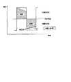
次に、液晶パネル15について説明をする。液晶パネル15は、図2に示すように、いわゆる透過型の液晶パネルであり、映像信号に応じた信号電圧が印加される透明な画素電極22が形成された画素電極基板21と、液晶層23を挟んで画素電極基板21と対向して配置され、対向電極24を有する対向基板25とを備える。液晶パネル15は、例えば、フレーム毎に各画素電極22に印加する電圧を対向電極電圧に対して反転させるフレーム反転駆動を行うアクティブマトリクス型液晶表示素子として構成される。 Next, the
液晶パネル15の液晶層23は、画素電極基板21と、対向基板25と、画素電極基板21と対向基板25との間において周囲を枠状に囲うシール材(不図示)とにより形成される空間に、封入される液晶26からなる。 The
画素電極基板21は、石英、ガラス、プラスチック等の透明材料からなり、対向基板25と対向する内面側に、TFT(Thin Film Transistor)と、このTFTに接続された画素電極22とが画素毎に設けられている。画素電極22は、ITO膜(インジウム・ティン・オキサイド膜)等の透明導電膜により形成されている。また、画素電極基板21の内面側には、画素電極22を覆うように、例えば、無機材料により形成され、液晶26の分子群を所定方向に配列させる配向膜27が設けられている。 The
対向基板25は、画素電極基板21と同様に、石英、ガラス、プラスチック等の透明材料からなり、画素電極基板21と対向する内面側に、対向電極24が設けられている。対向電極24は、ITO膜等の透明導電膜により形成されている。さらに、対向基板25の内面側には、対向電極24を覆うように、例えば、無機材料により形成され、液晶26の分子群を所定方向に配列させる配向膜28が設けられている。 Similar to the
また、液晶パネル15は、入射側及び出射側に、第1の偏光板29と第2の偏光板30とが設けられており、この第1及び第2の偏光板29、30により、液晶パネル15の画素電極基板21及び対向基板25を挟むように配設されている。 In addition, the
第1の偏光板29は、液晶パネル15の入射側に設けられ、光源11から出射された直線偏光光の偏光度を高める機能を有している。第2の偏光板30は、液晶パネル15からの出射側に設けられ、第1の偏光板29と同様に、液晶パネル15からの変調光の偏光度を高める機能を有している。 The first
続いて、液晶パネル15の駆動回路構成について、図3を参照して説明する。液晶パネル15は、画素電極基板21上に、図3に示すように、マトリクス状に配列された複数の画素スイッチSvh(v、hはそれぞれ自然数)と、画素容量Cvhと、画素電極Pvh(図2中、画素電極22)とからなる画素セル駆動回路と、シフトレジスタを備えた垂直駆動回路31と、水平駆動回路32と、垂直駆動回路31及び水平駆動回路32の駆動タイミング等の駆動を制御する駆動制御回路33とを備えている。液晶パネル15は、対向基板25の対向電極24に、共通電位Vcomが印加される。このような構成を有する液晶パネル15においては、画素電極Pvh毎に対応した液晶層23における表示領域が1つの画素を示す画素セルvhとなる。 Next, the drive circuit configuration of the
画素スイッチSvhのソース(S)は、画素容量Cvhを介して共通電極(図2中、対向電極24)と接続されている。また、画素スイッチSvhのソースと画素容量Cvhとの接続点には、画素電極Pvhが接続されている。さらに、画素スイッチSvhのゲート(G)に対しては、垂直駆動回路31から引き出されるゲート線Gvが接続され、ドレイン(D)に対しては、水平駆動回路32から引き出されるデータ線Dhが接続される。 The source (S) of the pixel switch Svh is connected to the common electrode (the
垂直駆動回路31は、シフトレジスタを備えており、このシフトレジスタから水平方向に引き出され、画素セルvhが備える画素スイッチSvhのゲートに接続されたゲート線G1、G2・・・Gvを順次走査する。また、水平駆動回路32は、シフトレジスタを備えており、このシフトレジスタから垂直方向に引き出され、画素セルvhが備える画素スイッチSvhのドレインに接続されたデータ線D1、D2・・・Dhを順次走査する。 The
駆動制御回路33は、垂直駆動タイミングパルス発生回路を有し、垂直駆動回路31のシフトレジスタに対して、垂直シフトクロックVC1、VC2・・・VCvを供給する。また、駆動制御回路33は、水平駆動タイミングパルス発生回路を有し、水平駆動回路32のシフトレジスタに対して、水平シフトクロックHC1、HC2・・・HChを供給する。 The drive control circuit 33 has a vertical drive timing pulse generation circuit, and supplies vertical shift clocks VC1, VC2,... VCv to the shift register of the
このような構成の液晶パネル15は、以下のようにして画素に電荷が書き込まれることになる。まず、垂直駆動回路31によってゲート線G1の電圧がハイになると、1行目の画素スイッチS11〜Svhがオンする。画素スイッチS11〜Svhがオンした後、水平駆動回路32によってデータ線D1がドライブされると、画素スイッチS11を介して画素容量C11にデータ(映像信号)が書き込まれる。 In the
次に、水平駆動回路32は、データ線D1のドライブをストップして、画素スイッチS11をオフにし、さらにデータ線D2をドライブして、画素スイッチS12をオンする。これにより、画素容量C11に書き込まれたデータ(映像信号)は保持されて、画素スイッチS12を介して画素容量C12にデータが書き込まれる。これを順次、データ線Dhまで繰り返すことにより水平方向の1両目の画素へデータを書き込むことができる。 Next, the
水平方向の1行目の画素へのデータ書き込みが終了したら、垂直駆動回路31は、ゲート線G1を立ち下げ、ゲート線G2を立ち上げる。垂直駆動回路31は、ゲート線G2が立ち上がったことに応じて、順次、データ線D1〜Dhをドライブして、上述したように水平方向の画素へのデータ書き込みを実行する。この動作を、ゲート線Gvまで全て繰り返すことにより、液晶パネル15の全ての画素に対してデータ(映像信号)の書き込みが実行される。 When the data writing to the pixels in the first row in the horizontal direction is completed, the
次に、上述のように構成される液晶パネル15の信号処理回路について説明をする。液晶パネル15の信号処理回路40は、図4に示すように、画像信号が入力端子Dinから入力され、その画像信号が、遅延調整回路41と、階調検出回路42とに供給される。また、信号処理回路40には、極性切替信号が供給される極性判別回路43と、色設定信号が供給される色判別回路44と、入射角設定信号が供給される入射角補正回路45とを備える。 Next, the signal processing circuit of the
遅延調整回路41は、入力端子Dinを介して画像信号が供給され、各補正信号との遅延量を調整、制御する回路である。 The
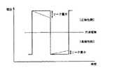
階調検出回路42は、遅延調整回路41と同様に、入力端子Dinを介して画像信号が供給され、画像信号の階調を検出し、検出された階調に応じて階調補正値HGを算出する。階調検出回路42は、図5に示すように、階調に応じて変動する電圧値の大小によりリーク量も増減することになり、この階調、すなわち、電圧値の大小を検出し、電圧値が大きい場合には、リーク量を少なくし、電圧値が小さい場合と同量のリーク量となるように適正な階調補正値HGを算出する。 Similar to the
極性判別回路43は、垂直駆動回路31によって行われる垂直走査の周期毎に所定の電位レベルに対して極性を切り替える極性切替信号が、入力端子Ginを介して供給され、供給される極性切替信号に応じて、正極性か負極性かを判別し、極性補正値HPを算出する。極性判別回路43は、図6に示すように、リーク量が、極性に応じて異なる、すなわち、正極性側が負極性側よりも多くなることから、極性を判別し、正極性の場合には、負極性と同量のリーク量となるように補正する、極性に応じた極性補正値HPを算出する。 The
色判別回路44は、供給される画像信号に対応する色設定信号が、入力端子Cinを介して供給され、供給された色設定信号に応じて、当該画像信号の色判別を行う。具体的には、色判別回路44は、画像信号の波長・輝度を検出、判別し、この波長・輝度に応じた色補正値HCを算出する。色判別回路44は、図7に示すように、リーク量が、光の波長に応じて異なる、すなわち、短波長が長波長よりも多くなることから、色(波長、輝度)を検出、判別し、短波長の場合には、長波長と同量のリーク量となるように補正する、色に応じた色補正値HCを算出する。 The
入射角補正回路45は、供給される画像信号に対応する入射角設定信号が、入力端子Ainを介して供給され、供給された入射角設定信号に応じて、各画素セルvhに入射される光の入射角度を検出し、当該入射角度に応じて入射角補正値HAを算出する。入射角補正回路45は、画素セルvhに入射される光が、図1に示すように、色分離部14の各ミラーに応じて入射角が異なり、このとき、図8に示すように、リーク量が、入射角度に応じて異なる、すなわち、入射角度が大きいほどリーク量も多くなることから、当該入射角度を検出し、入射角が大きい場合には、入射角が小さい場合と同量のリーク量となるように補正する、入射角度に応じた入射角補正値HAを算出する。 The incident
信号処理回路40では、各回路42〜45において算出される補正値HG、HP、HC、HAを加算することにより求められる補正値Hが、遅延調整回路41において遅延制御された画像信号と加算することにより、図9に示すように、正極性側と負極性側の積分値が等しくなるように補正される。 In the
なお、図9においては、負極性側の値を補正値Hにより補正することについて示したが、これに限らず、正極性側を補正するようにしてもよく、さらには、両極性ともに、補正するようにしてもよい。 In FIG. 9, correction of the negative polarity value by the correction value H is shown. However, the present invention is not limited to this, and the positive polarity side may be corrected. You may make it do.
以上のような構成を備える映像表示装置1は、リーク電流を発生させる要因として考えられる、階調、極性、色(波長、輝度)、入射角等を勘案し、これらの値に応じた補正値を算出することができるので、確実に画質劣化や、輝度変化によるフリッカや、直流成分の印加による焼き付きを防止することができ、液晶の品質劣化を防止することができる。 The video display device 1 having the above-described configuration takes into account the gradation, polarity, color (wavelength, luminance), incident angle, and the like, which are considered as factors that cause leakage current, and correction values according to these values. Therefore, it is possible to reliably prevent image quality deterioration, flicker due to luminance change, and burn-in due to application of a DC component, and to prevent deterioration of liquid crystal quality.
なお、本発明においては、いわゆる透過型の液晶表示素子についての実施の形態について説明をしたが、これに限らず、反射型の液晶表示素子を用いるものであってもよい。また、その際、本説明においては、短波長においてはリーク量が大きくなり、長波長においてはリーク量が小さくなる旨の実施の形態について示したが、液晶表示素子の構造によっては、リーク量が逆、すなわち短波長においてはリーク量が小さくなり、長波長においてはリーク量が大きくなる場合もある。 In the present invention, an embodiment of a so-called transmissive liquid crystal display element has been described. However, the present invention is not limited to this, and a reflective liquid crystal display element may be used. At this time, in the present description, the embodiment has been shown in which the amount of leakage increases at short wavelengths and the amount of leakage decreases at long wavelengths. However, depending on the structure of the liquid crystal display element, the amount of leakage may be small. Conversely, the leak amount may be small at short wavelengths and the leak amount may be large at long wavelengths.
1 映像表示装置、11 光源、12 リフレクタ、13 コンデンサレンズ、14 色分離部、14B ダイクロイックミラー、14G 反射ミラー、14R ダイクロイックミラー、15 液晶パネル、15a マイクロレンズアレイ、16 投写レンズ、17 スクリーン、21 画素電極基板、22 画素電極、23 液晶層、24 対向電極、25 対向基板、26 液晶、27、28 配向膜、29、30 偏光板、31 垂直駆動回路、32 水平駆動回路、33 駆動制御回路、40 信号処理回路、41 遅延調整回路、42 階調検出回路、43 極性判別回路、44 色判別回路、45 入射角補正回路 DESCRIPTION OF SYMBOLS 1 Image display apparatus, 11 Light source, 12 Reflector, 13 Condenser lens, 14 Color separation part, 14B Dichroic mirror, 14G Reflection mirror, 14R Dichroic mirror, 15 Liquid crystal panel, 15a Micro lens array, 16 Projection lens, 17 Screen, 21 pixels Electrode substrate, 22 pixel electrode, 23 liquid crystal layer, 24 counter electrode, 25 counter substrate, 26 liquid crystal, 27, 28 alignment film, 29, 30 polarizing plate, 31 vertical drive circuit, 32 horizontal drive circuit, 33 drive control circuit, 40 Signal processing circuit, 41 delay adjustment circuit, 42 gradation detection circuit, 43 polarity discrimination circuit, 44 color discrimination circuit, 45 incident angle correction circuit
Claims (4)
Translated fromJapanese上記信号生成手段は、
上記液晶表示素子の着目画素に入力される画像信号の階調を検出し、該検出された階調により、第1の補正値を算出する第1の補正手段と、
上記液晶表示素子の着目画素に入力される画像信号に対応して上記第1の電極と上記第2の電極との間に印加される電圧成分の極性を検出し、該検出された極性により、第2の補正値を算出する第2の補正手段と、
上記液晶表示素子の着目画素に上記光源から照射される光の波長及び/又は輝度を検出し、該検出された波長及び/又は輝度により、第3の補正値を算出する第3の補正手段と、
上記第1乃至第3の補正手段により算出された上記第1乃至第3の補正値により、上記第1の電極と上記第2の電極との間に印加される電圧成分を補正する補正値を算出する補正値算出手段とを備えることを特徴とする映像表示装置。A light source; a liquid crystal display element that optically modulates light emitted from the light source; and a signal generation unit that generates a signal for driving the liquid crystal display element in accordance with an input image signal to optically modulate incident light. The liquid crystal display element includes: a first substrate having a first electrode; a second substrate having a second electrode disposed opposite to the first substrate; the first substrate; In an image display device which is an active matrix type liquid crystal display element comprising a liquid crystal layer held between two substrates,
The signal generating means includes
First correction means for detecting a gradation of an image signal input to the pixel of interest of the liquid crystal display element and calculating a first correction value based on the detected gradation;
The polarity of the voltage component applied between the first electrode and the second electrode corresponding to the image signal input to the pixel of interest of the liquid crystal display element is detected, and the detected polarity Second correction means for calculating a second correction value;
Third correction means for detecting a wavelength and / or luminance of light emitted from the light source to the pixel of interest of the liquid crystal display element, and calculating a third correction value based on the detected wavelength and / or luminance; ,
A correction value for correcting a voltage component applied between the first electrode and the second electrode is calculated based on the first to third correction values calculated by the first to third correction means. An image display device comprising correction value calculation means for calculating.
上記信号生成手段は、
上記液晶表示素子の着目画素に入力される画像信号の階調を検出し、該検出された階調により、第1の補正値を算出する第1の補正手段と、
上記液晶表示素子の着目画素に入力される画像信号に対応して上記第1の電極と上記第2の電極との間に印加される電圧成分の極性を検出し、該検出された極性により、第2の補正値を算出する第2の補正手段と、
上記液晶表示素子の着目画素に、上記色分離部を介して上記光源から照射される光の波長及び/又は輝度を検出し、該検出された波長及び/又は輝度により、第3の補正値を算出する第3の補正手段と、
上記液晶表示素子の着目画素に、上記色分離部を介して上記光源から照射される光の入射角を検出し、該検出された入射角により第4の補正値を算出する第4の補正手段と、
上記第1乃至第4の補正手段により算出された上記第1乃至第4の補正値により、上記第1の電極と上記第2の電極との間に印加される電圧成分を補正する補正値を算出する補正値算出手段とを備えることを特徴とする映像表示装置。A light source, a color separation unit that color-separates light emitted from the light source, a liquid crystal display element that optically modulates each light color-separated by the color separation unit, and the liquid crystal display according to an input image signal Signal generating means for driving the element and generating a signal for optically modulating incident light, and the liquid crystal display element is disposed opposite to the first substrate having the first electrode and the first substrate. In an image display device which is an active matrix type liquid crystal display element including a second substrate having a second electrode and a liquid crystal layer held between the first substrate and the second substrate,
The signal generating means includes
First correction means for detecting a gradation of an image signal input to the pixel of interest of the liquid crystal display element and calculating a first correction value based on the detected gradation;
The polarity of the voltage component applied between the first electrode and the second electrode corresponding to the image signal input to the pixel of interest of the liquid crystal display element is detected, and the detected polarity Second correction means for calculating a second correction value;
A wavelength and / or luminance of light emitted from the light source to the target pixel of the liquid crystal display element via the color separation unit is detected, and a third correction value is set based on the detected wavelength and / or luminance. A third correction means for calculating;
Fourth correction means for detecting an incident angle of light emitted from the light source to the target pixel of the liquid crystal display element via the color separation unit, and calculating a fourth correction value based on the detected incident angle. When,
A correction value for correcting a voltage component applied between the first electrode and the second electrode by the first to fourth correction values calculated by the first to fourth correction means. An image display device comprising correction value calculation means for calculating.
上記液晶表示素子の着目画素に入力される画像信号の階調を検出し、該検出された階調により、第1の補正値を算出する第1の補正値算出ステップと、
上記液晶表示素子の着目画素に入力される画像信号に対応して上記第1の電極と上記第2の電極との間に印加される電圧成分の極性を検出し、該検出された極性により、第2の補正値を算出する第2の補正値算出ステップと、
上記液晶表示素子の着目画素に上記光源から照射される光の波長及び/又は輝度を検出し、該検出された波長及び/又は輝度により、第3の補正値を算出する第3の補正値算出ステップと、
上記第1乃至第3の補正手段により算出された上記第1乃至第3の補正値により、上記第1の電極と上記第2の電極との間に印加される電圧成分を補正する補正値を算出する補正値算出ステップとを有することを特徴とする映像表示装置の駆動方法。A light source; a liquid crystal display element that optically modulates light emitted from the light source; and a signal generation unit that generates a signal for driving the liquid crystal display element in accordance with an input image signal to optically modulate incident light. The liquid crystal display element includes: a first substrate having a first electrode; a second substrate having a second electrode disposed opposite to the first substrate; the first substrate; In a driving method of a video display device which is an active matrix type liquid crystal display element comprising a liquid crystal layer held between two substrates,
A first correction value calculating step of detecting a gradation of an image signal input to the pixel of interest of the liquid crystal display element and calculating a first correction value based on the detected gradation;
The polarity of the voltage component applied between the first electrode and the second electrode corresponding to the image signal input to the pixel of interest of the liquid crystal display element is detected, and the detected polarity A second correction value calculating step for calculating a second correction value;
Third correction value calculation for detecting a wavelength and / or luminance of light emitted from the light source to the pixel of interest of the liquid crystal display element, and calculating a third correction value based on the detected wavelength and / or luminance. Steps,
A correction value for correcting a voltage component applied between the first electrode and the second electrode is calculated based on the first to third correction values calculated by the first to third correction means. And a correction value calculating step for calculating the image display device.
上記液晶表示素子の着目画素に入力される画像信号の階調を検出し、該検出された階調により、第1の補正値を算出する第1の補正値算出ステップと、
上記液晶表示素子の着目画素に入力される画像信号に対応して上記第1の電極と上記第2の電極との間に印加される電圧成分の極性を検出し、該検出された極性により、第2の補正値を算出する第2の補正値算出ステップと、
上記液晶表示素子の着目画素に、上記色分離部を介して上記光源から照射される光の波長及び/又は輝度を検出し、該検出された波長及び/又は輝度により、第3の補正値を算出する第3の補正値算出ステップと、
上記液晶表示素子の着目画素に、上記色分離部を介して上記光源から照射される光の入射角を検出し、該検出された入射角により第4の補正値を算出する第4の補正値算出ステップと、
上記第1乃至第4の補正手段により算出された上記第1乃至第4の補正値により、上記第1の電極と上記第2の電極との間に印加される電圧成分を補正する補正値を算出する補正値算出ステップとを有することを特徴とする映像表示装置の駆動方法。A light source, a color separation unit that color-separates light emitted from the light source, a liquid crystal display element that optically modulates each light color-separated by the color separation unit, and the liquid crystal display according to an input image signal Signal generating means for driving the element and generating a signal for optically modulating incident light, and the liquid crystal display element is disposed opposite to the first substrate having the first electrode and the first substrate. And a driving method of a video display device, which is an active matrix type liquid crystal display element, comprising: a second substrate having a second electrode; and a liquid crystal layer held between the first substrate and the second substrate. In
A first correction value calculating step of detecting a gradation of an image signal input to the pixel of interest of the liquid crystal display element and calculating a first correction value based on the detected gradation;
The polarity of the voltage component applied between the first electrode and the second electrode corresponding to the image signal input to the pixel of interest of the liquid crystal display element is detected, and the detected polarity A second correction value calculating step for calculating a second correction value;
A wavelength and / or luminance of light emitted from the light source to the target pixel of the liquid crystal display element via the color separation unit is detected, and a third correction value is set based on the detected wavelength and / or luminance. A third correction value calculating step for calculating;
A fourth correction value for detecting an incident angle of light emitted from the light source to the target pixel of the liquid crystal display element via the color separation unit and calculating a fourth correction value based on the detected incident angle; A calculation step;
A correction value for correcting a voltage component applied between the first electrode and the second electrode by the first to fourth correction values calculated by the first to fourth correction means. And a correction value calculating step for calculating the image display device.
Priority Applications (5)
| Application Number | Priority Date | Filing Date | Title |
|---|---|---|---|
| JP2007321212AJP2009145500A (en) | 2007-12-12 | 2007-12-12 | Video display apparatus and method for driving the same |
| US12/289,996US20090153457A1 (en) | 2007-12-12 | 2008-11-10 | Display apparatus and method for driving the same |
| TW097143541ATWI399579B (en) | 2007-12-12 | 2008-11-11 | Display apparatus and method for driving the same |
| KR1020080119415AKR20090063097A (en) | 2007-12-12 | 2008-11-28 | Display device and driving method |
| CNA2008101867117ACN101458413A (en) | 2007-12-12 | 2008-12-12 | Display apparatus and method for driving the same |
Applications Claiming Priority (1)
| Application Number | Priority Date | Filing Date | Title |
|---|---|---|---|
| JP2007321212AJP2009145500A (en) | 2007-12-12 | 2007-12-12 | Video display apparatus and method for driving the same |
Publications (1)
| Publication Number | Publication Date |
|---|---|
| JP2009145500Atrue JP2009145500A (en) | 2009-07-02 |
Family
ID=40752525
Family Applications (1)
| Application Number | Title | Priority Date | Filing Date |
|---|---|---|---|
| JP2007321212APendingJP2009145500A (en) | 2007-12-12 | 2007-12-12 | Video display apparatus and method for driving the same |
Country Status (5)
| Country | Link |
|---|---|
| US (1) | US20090153457A1 (en) |
| JP (1) | JP2009145500A (en) |
| KR (1) | KR20090063097A (en) |
| CN (1) | CN101458413A (en) |
| TW (1) | TWI399579B (en) |
Families Citing this family (9)
| Publication number | Priority date | Publication date | Assignee | Title |
|---|---|---|---|---|
| KR100886557B1 (en)* | 2007-05-03 | 2009-03-02 | 삼성전자주식회사 | Face Recognition System and Method Based on Adaptive Learning |
| US8493057B2 (en) | 2009-05-15 | 2013-07-23 | Advantest Corporation | Electromagnetic wave measuring apparatus, measuring method, program, and recording medium |
| JP5617262B2 (en)* | 2010-02-02 | 2014-11-05 | セイコーエプソン株式会社 | Liquid crystal device, liquid crystal device control method, and electronic apparatus |
| GB2480874B (en)* | 2010-06-04 | 2017-07-12 | Flexenable Ltd | Tuning Display Devices |
| KR20150059686A (en)* | 2013-11-22 | 2015-06-02 | 삼성전자주식회사 | Method and apparatus for image processing |
| CN104599632B (en)* | 2015-01-05 | 2017-10-27 | 昆山国显光电有限公司 | Improve the method and device of OLED display brightness uniformities |
| CN107238929A (en)* | 2017-07-17 | 2017-10-10 | 深圳市世尊科技有限公司 | Wearable system |
| CN110827733B (en)* | 2018-08-07 | 2023-11-14 | 奇景光电股份有限公司 | Display method and display device for display panel |
| JP7239460B2 (en)* | 2019-12-24 | 2023-03-14 | パナソニック液晶ディスプレイ株式会社 | Image processing device and liquid crystal display device |
Family Cites Families (7)
| Publication number | Priority date | Publication date | Assignee | Title |
|---|---|---|---|---|
| JPH0667153A (en)* | 1992-08-21 | 1994-03-11 | Matsushita Electric Ind Co Ltd | Matrix-type display drive device and projection-type image display device using the device |
| US5597223A (en)* | 1993-12-27 | 1997-01-28 | Kabushiki Kaisha Toshiba | Display apparatus |
| JP2002182008A (en)* | 2000-10-04 | 2002-06-26 | Sharp Corp | Optical lens system, image display device, microlens array, liquid crystal display element, and projection type liquid crystal display device |
| JP3771157B2 (en)* | 2000-10-13 | 2006-04-26 | シャープ株式会社 | Display device driving method and liquid crystal display device driving method |
| JP3473600B2 (en)* | 2000-12-01 | 2003-12-08 | セイコーエプソン株式会社 | Liquid crystal display device, image data correction circuit, image data correction method, and electronic device |
| JP4493274B2 (en)* | 2003-01-29 | 2010-06-30 | 富士通株式会社 | Display device and display method |
| JP4052282B2 (en)* | 2004-05-07 | 2008-02-27 | セイコーエプソン株式会社 | projector |
- 2007
- 2007-12-12JPJP2007321212Apatent/JP2009145500A/enactivePending
- 2008
- 2008-11-10USUS12/289,996patent/US20090153457A1/ennot_activeAbandoned
- 2008-11-11TWTW097143541Apatent/TWI399579B/ennot_activeIP Right Cessation
- 2008-11-28KRKR1020080119415Apatent/KR20090063097A/ennot_activeCeased
- 2008-12-12CNCNA2008101867117Apatent/CN101458413A/enactivePending
Also Published As
| Publication number | Publication date |
|---|---|
| TWI399579B (en) | 2013-06-21 |
| KR20090063097A (en) | 2009-06-17 |
| CN101458413A (en) | 2009-06-17 |
| US20090153457A1 (en) | 2009-06-18 |
| TW200928493A (en) | 2009-07-01 |
Similar Documents
| Publication | Publication Date | Title |
|---|---|---|
| JP4923866B2 (en) | Liquid crystal display device and video display device | |
| TWI399579B (en) | Display apparatus and method for driving the same | |
| TWI393945B (en) | Video signal processing circuit, display apparatus, liquid crystal display apparatus, projection type display apparatus, and video signal processing method | |
| US5805243A (en) | Liquid crystal projector using a spatial light modulator and two rotating color filters | |
| US7581836B2 (en) | Image display device and projector | |
| US11595627B2 (en) | Liquid crystal projector | |
| JP4799629B2 (en) | Projection display device | |
| JP5790256B2 (en) | Electro-optical device, driving method of electro-optical device, electronic apparatus, projector | |
| JP2008268904A (en) | Liquid crystal display | |
| JP2008292861A (en) | Liquid crystal display device and video display device | |
| JP6642618B2 (en) | Electro-optical devices, projection display devices | |
| JP2008268253A (en) | Liquid crystal display device, method for driving liquid crystal display device, and video display device | |
| US7319439B2 (en) | Image display device and projector | |
| CN100394264C (en) | Image display device and method for driving liquid crystal panel | |
| US20150222863A1 (en) | Projector | |
| US12236909B2 (en) | Drive circuit of display panel, display device, and drive method of display panel | |
| JP2005195832A (en) | Image display apparatus and image display method | |
| JP2002357809A (en) | Image display device | |
| JP2011197384A (en) | Liquid crystal driving device, liquid crystal display device, and projector | |
| JP2022190312A (en) | Display and method for controlling display | |
| JP2009151190A (en) | Liquid crystal display, its manufacturing method, and image display | |
| KR100557638B1 (en) | Optical system of 3 plate type liquid crystal projector | |
| JP2013057823A (en) | Spatial optical modulation element, and projection display device | |
| KR100841327B1 (en) | Liquid crystal display device and driving method thereof | |
| JP2008288496A (en) | Liquid crystal display unit and manufacturing method thereof, video display unit and manufacturing method thereof |
Legal Events
| Date | Code | Title | Description |
|---|---|---|---|
| A977 | Report on retrieval | Free format text:JAPANESE INTERMEDIATE CODE: A971007 Effective date:20091029 | |
| A131 | Notification of reasons for refusal | Free format text:JAPANESE INTERMEDIATE CODE: A131 Effective date:20091104 | |
| A02 | Decision of refusal | Free format text:JAPANESE INTERMEDIATE CODE: A02 Effective date:20100309 |