JP2009130216A - Magnetic device and frequency detector - Google Patents
Magnetic device and frequency detectorDownload PDFInfo
- Publication number
- JP2009130216A JP2009130216AJP2007305010AJP2007305010AJP2009130216AJP 2009130216 AJP2009130216 AJP 2009130216AJP 2007305010 AJP2007305010 AJP 2007305010AJP 2007305010 AJP2007305010 AJP 2007305010AJP 2009130216 AJP2009130216 AJP 2009130216A
- Authority
- JP
- Japan
- Prior art keywords
- layer
- magnetization
- magnetic device
- magnetization free
- effect element
- Prior art date
- Legal status (The legal status is an assumption and is not a legal conclusion. Google has not performed a legal analysis and makes no representation as to the accuracy of the status listed.)
- Pending
Links
Images


Classifications
- G—PHYSICS
- G01—MEASURING; TESTING
- G01R—MEASURING ELECTRIC VARIABLES; MEASURING MAGNETIC VARIABLES
- G01R33/00—Arrangements or instruments for measuring magnetic variables
- G01R33/02—Measuring direction or magnitude of magnetic fields or magnetic flux
- G01R33/06—Measuring direction or magnitude of magnetic fields or magnetic flux using galvano-magnetic devices
- G01R33/09—Magnetoresistive devices
- G01R33/093—Magnetoresistive devices using multilayer structures, e.g. giant magnetoresistance sensors
- B—PERFORMING OPERATIONS; TRANSPORTING
- B82—NANOTECHNOLOGY
- B82Y—SPECIFIC USES OR APPLICATIONS OF NANOSTRUCTURES; MEASUREMENT OR ANALYSIS OF NANOSTRUCTURES; MANUFACTURE OR TREATMENT OF NANOSTRUCTURES
- B82Y25/00—Nanomagnetism, e.g. magnetoimpedance, anisotropic magnetoresistance, giant magnetoresistance or tunneling magnetoresistance
- H—ELECTRICITY
- H01—ELECTRIC ELEMENTS
- H01F—MAGNETS; INDUCTANCES; TRANSFORMERS; SELECTION OF MATERIALS FOR THEIR MAGNETIC PROPERTIES
- H01F10/00—Thin magnetic films, e.g. of one-domain structure
- H01F10/32—Spin-exchange-coupled multilayers, e.g. nanostructured superlattices
- H01F10/324—Exchange coupling of magnetic film pairs via a very thin non-magnetic spacer, e.g. by exchange with conduction electrons of the spacer
- H01F10/3254—Exchange coupling of magnetic film pairs via a very thin non-magnetic spacer, e.g. by exchange with conduction electrons of the spacer the spacer being semiconducting or insulating, e.g. for spin tunnel junction [STJ]
- H01F10/3259—Spin-exchange-coupled multilayers comprising at least a nanooxide layer [NOL], e.g. with a NOL spacer
- H—ELECTRICITY
- H10—SEMICONDUCTOR DEVICES; ELECTRIC SOLID-STATE DEVICES NOT OTHERWISE PROVIDED FOR
- H10B—ELECTRONIC MEMORY DEVICES
- H10B61/00—Magnetic memory devices, e.g. magnetoresistive RAM [MRAM] devices
- H—ELECTRICITY
- H10—SEMICONDUCTOR DEVICES; ELECTRIC SOLID-STATE DEVICES NOT OTHERWISE PROVIDED FOR
- H10N—ELECTRIC SOLID-STATE DEVICES NOT OTHERWISE PROVIDED FOR
- H10N50/00—Galvanomagnetic devices
- H10N50/10—Magnetoresistive devices
- H—ELECTRICITY
- H10—SEMICONDUCTOR DEVICES; ELECTRIC SOLID-STATE DEVICES NOT OTHERWISE PROVIDED FOR
- H10N—ELECTRIC SOLID-STATE DEVICES NOT OTHERWISE PROVIDED FOR
- H10N59/00—Integrated devices, or assemblies of multiple devices, comprising at least one galvanomagnetic or Hall-effect element covered by groups H10N50/00 - H10N52/00
- G—PHYSICS
- G01—MEASURING; TESTING
- G01R—MEASURING ELECTRIC VARIABLES; MEASURING MAGNETIC VARIABLES
- G01R23/00—Arrangements for measuring frequencies; Arrangements for analysing frequency spectra
- G01R23/02—Arrangements for measuring frequency, e.g. pulse repetition rate; Arrangements for measuring period of current or voltage
- G01R23/06—Arrangements for measuring frequency, e.g. pulse repetition rate; Arrangements for measuring period of current or voltage by converting frequency into an amplitude of current or voltage
- G01R23/07—Arrangements for measuring frequency, e.g. pulse repetition rate; Arrangements for measuring period of current or voltage by converting frequency into an amplitude of current or voltage using response of circuits tuned on resonance, e.g. grid-drip meter
- H—ELECTRICITY
- H01—ELECTRIC ELEMENTS
- H01F—MAGNETS; INDUCTANCES; TRANSFORMERS; SELECTION OF MATERIALS FOR THEIR MAGNETIC PROPERTIES
- H01F10/00—Thin magnetic films, e.g. of one-domain structure
- H01F10/08—Thin magnetic films, e.g. of one-domain structure characterised by magnetic layers
- H01F10/10—Thin magnetic films, e.g. of one-domain structure characterised by magnetic layers characterised by the composition
- H01F10/18—Thin magnetic films, e.g. of one-domain structure characterised by magnetic layers characterised by the composition being compounds
- H01F10/193—Magnetic semiconductor compounds
- H01F10/1936—Half-metallic, e.g. epitaxial CrO2 or NiMnSb films
- H—ELECTRICITY
- H01—ELECTRIC ELEMENTS
- H01F—MAGNETS; INDUCTANCES; TRANSFORMERS; SELECTION OF MATERIALS FOR THEIR MAGNETIC PROPERTIES
- H01F10/00—Thin magnetic films, e.g. of one-domain structure
- H01F10/32—Spin-exchange-coupled multilayers, e.g. nanostructured superlattices
- H01F10/324—Exchange coupling of magnetic film pairs via a very thin non-magnetic spacer, e.g. by exchange with conduction electrons of the spacer
- H01F10/3268—Exchange coupling of magnetic film pairs via a very thin non-magnetic spacer, e.g. by exchange with conduction electrons of the spacer the exchange coupling being asymmetric, e.g. by use of additional pinning, by using antiferromagnetic or ferromagnetic coupling interface, i.e. so-called spin-valve [SV] structure, e.g. NiFe/Cu/NiFe/FeMn
- H01F10/3272—Exchange coupling of magnetic film pairs via a very thin non-magnetic spacer, e.g. by exchange with conduction electrons of the spacer the exchange coupling being asymmetric, e.g. by use of additional pinning, by using antiferromagnetic or ferromagnetic coupling interface, i.e. so-called spin-valve [SV] structure, e.g. NiFe/Cu/NiFe/FeMn by use of anti-parallel coupled [APC] ferromagnetic layers, e.g. artificial ferrimagnets [AFI], artificial [AAF] or synthetic [SAF] anti-ferromagnets
Landscapes
- Chemical & Material Sciences (AREA)
- Engineering & Computer Science (AREA)
- Crystallography & Structural Chemistry (AREA)
- Nanotechnology (AREA)
- Physics & Mathematics (AREA)
- Power Engineering (AREA)
- Condensed Matter Physics & Semiconductors (AREA)
- General Physics & Mathematics (AREA)
- Hall/Mr Elements (AREA)
- Measuring Frequencies, Analyzing Spectra (AREA)
Abstract
Description
Translated fromJapanese本発明は、磁気デバイス及び周波数検出器に関する。 The present invention relates to a magnetic device and a frequency detector.
磁気抵抗効果素子として、磁化の向きが固定された固定層と、磁化の向きが自由に変化する磁化自由層(磁化自由層)との間に非磁性導電層を介在させてなるGMR(Giant Magnetoresistive)素子が知られている。また、別の磁気抵抗効果素子として、固定層と磁化自由層との間に非磁性絶縁層を介在させてなるTMR(Tunnel Magnetoresistive)素子が知られている。これらの磁気抵抗効果素子に電流を流すと、スピン偏極電流が流れ、磁化自由層内に蓄積されたスピンとの相互作用によりトルクが発生し、スピン偏極電流の極性に応じて、磁化自由層の磁化の向きが変更する。一定の磁場内に配置された磁化自由層では、その磁化の向きを変更しようとしても、磁場によって拘束される安定な方向へ復元するように、磁化の向きにトルクが働く。この磁化の向きの運動は、重力によって引っ張られた振り子の重りが、特定の力で揺らされると、ゆらゆらと振動するのに似ており、歳差運動と呼ばれる。 As a magnetoresistive effect element, a GMR (Giant Magnetoresistive) in which a nonmagnetic conductive layer is interposed between a fixed layer in which the magnetization direction is fixed and a magnetization free layer (magnetization free layer) in which the magnetization direction freely changes. ) The device is known. As another magnetoresistive effect element, a TMR (Tunnel Magnetoresistive) element is known in which a nonmagnetic insulating layer is interposed between a fixed layer and a magnetization free layer. When a current is passed through these magnetoresistive elements, a spin-polarized current flows, and torque is generated by interaction with the spin accumulated in the magnetization free layer. Depending on the polarity of the spin-polarized current, magnetization free The magnetization direction of the layer changes. In the magnetization free layer arranged in a constant magnetic field, even if the magnetization direction is changed, a torque acts on the magnetization direction so that the magnetization direction is restored in a stable direction constrained by the magnetic field. This movement in the direction of magnetization resembles that the weight of a pendulum pulled by gravity oscillates swaying with a specific force, and is called precession.
近年、この磁化の向きの歳差運動の固有振動数と、磁化自由層に流れる交流電流の周波数とが一致すると、共振が生じる現象が発見された(非特許文献1参照)。TMR素子の抵抗値は、磁化自由層の磁化の向きと、固定層の磁化の向きとが成す角度に依存する。磁化自由層において磁化の向きの共振が生じると、磁化自由層の磁化の向きは大きく振動し、TMR素子の抵抗値が周期的に大きく変動する。一方、入力される交流電流に同期してTMR素子の抵抗値が大きく変動すると、TMR素子の両端間を流れる交流電流がゼロレベルに対して非対称に変動して直流成分を有するようになり、変動分を出力として取り出すことができる(スピントルクダイオード効果)。
上述のように磁気抵抗効果素子がスピントルクダイオード効果を発揮する場合、出力直流電圧は、入力される交流電圧の特定の周波数領域においてピークを有することとなる。そして、スピントルクダイオード効果を応用した磁気デバイスにおいては、このような出力直流電圧のピークの半値幅は小さい程好ましい。 As described above, when the magnetoresistive element exhibits the spin torque diode effect, the output DC voltage has a peak in a specific frequency region of the input AC voltage. And in the magnetic device which applied the spin torque diode effect, the half value width of the peak of such an output DC voltage is so preferable that it is small.
しかしながら、従来のスピントルクダイオード効果を発揮する磁気抵抗効果素子においては、出力される直流電圧のピークの半値幅が十分に小さいとは言えず、また、出力直流電圧のピークの半値幅を小さくする素子構成も知られていなかった。 However, in the conventional magnetoresistive effect element exhibiting the spin torque diode effect, it cannot be said that the half width of the peak of the output DC voltage is sufficiently small, and the half width of the peak of the output DC voltage is reduced. The element configuration was not known.
本発明は、このような課題に鑑みてなされたものであり、出力直流電圧のピークの半値幅が十分に小さいスピントルクダイオード効果を利用した磁気デバイス、及び、このような磁気デバイスを利用した周波数検出器を提供することを目的とする。 The present invention has been made in view of such problems, and a magnetic device using the spin torque diode effect in which the half width of the peak of the output DC voltage is sufficiently small, and a frequency using such a magnetic device. An object is to provide a detector.
上述の課題を解決するため、本発明に係る磁気デバイスは、磁化固定層、磁化自由層、及び磁化固定層と磁化自由層とに挟まれた非磁性層を有する磁気抵抗効果素子と、磁気抵抗効果素子に対して、その積層方向に交流信号を流すための入力端子と、磁気抵抗効果素子から出力電圧を取り出す出力端子とを備え、非磁性層は、絶縁体からなる絶縁層部と、絶縁層部をその膜厚方向に貫通する導電体からなる電流狭窄層部とを含むことを特徴とする。 In order to solve the above-described problems, a magnetic device according to the present invention includes a magnetoresistive element having a magnetization fixed layer, a magnetization free layer, and a nonmagnetic layer sandwiched between the magnetization fixed layer and the magnetization free layer, and a magnetoresistance The effect element has an input terminal for flowing an AC signal in the stacking direction and an output terminal for extracting an output voltage from the magnetoresistive effect element. The nonmagnetic layer is insulated from an insulating layer portion made of an insulator. And a current confinement layer portion made of a conductor that penetrates the layer portion in the film thickness direction.
本発明の磁気デバイスによれば、磁気抵抗効果素子に電流を流すとスピン偏極電流が流れ、磁化自由層と磁化自由層内に蓄積されたスピンとの相互作用によりトルクが発生し、スピン偏極電流の極性に応じて、磁化自由層の磁化の向きが変更する。そして、磁気抵抗効果素子の磁化自由層の磁化の向きの固有振動数と、磁気抵抗効果素子を流れる交流電流の周波数が一致した場合、磁化自由層の磁化の向きの振動が共振する。この際、磁気抵抗効果素子の抵抗値は磁化自由層の磁化の向きと磁化固定層の磁化の向きの相対的な角度に依存する。その結果、磁気抵抗効果素子の抵抗値はその周波数で急激に変動することとなり、出力電圧はゼロレベルに対して非対称に変動して直流成分を有することとなる。 According to the magnetic device of the present invention, when a current is passed through the magnetoresistive effect element, a spin-polarized current flows, and torque is generated by the interaction between the magnetization free layer and the spin accumulated in the magnetization free layer. The magnetization direction of the magnetization free layer changes according to the polarity of the polar current. When the natural frequency of the magnetization direction of the magnetization free layer of the magnetoresistive effect element matches the frequency of the alternating current flowing through the magnetoresistive effect element, the vibration of the magnetization direction of the magnetization free layer resonates. At this time, the resistance value of the magnetoresistive element depends on the relative angle between the magnetization direction of the magnetization free layer and the magnetization direction of the magnetization fixed layer. As a result, the resistance value of the magnetoresistive effect element fluctuates abruptly at the frequency, and the output voltage fluctuates asymmetrically with respect to the zero level and has a direct current component.
そして、本発明の磁気デバイスでは、入力された交流信号の電流は、磁気抵抗効果素子の非磁性層を通過する際、非磁性層の絶縁層部を通過することはできず、電流狭窄層部のみを通過することとなる。そのため、出力直流電圧のピークの半値幅は十分に小さくなる。 In the magnetic device of the present invention, when the current of the input AC signal passes through the nonmagnetic layer of the magnetoresistive effect element, it cannot pass through the insulating layer portion of the nonmagnetic layer. Will only pass through. Therefore, the half width of the peak of the output DC voltage is sufficiently small.
さらに、磁気デバイスは、磁化自由層に磁界を印加するように設けられた磁界印加部をさらに備えていることが好ましい。 Furthermore, it is preferable that the magnetic device further includes a magnetic field applying unit provided so as to apply a magnetic field to the magnetization free layer.
これにより、磁化自由層に所定の大きさの磁場を印加することができる。そして、磁化自由層の磁化の向きの固有振動数(共振周波数)は、磁化自由層に印加される磁場の大きさに依存して決定される。そのため、入力された交流信号のうち、決定された共振周波数の成分に対応する特定の周波数の信号の電圧を選択的に変動させて直流成分を出力する磁気デバイスが得られる。 Thereby, a magnetic field of a predetermined magnitude can be applied to the magnetization free layer. The natural frequency (resonance frequency) of the magnetization direction of the magnetization free layer is determined depending on the magnitude of the magnetic field applied to the magnetization free layer. Therefore, a magnetic device that outputs a DC component by selectively changing the voltage of a signal having a specific frequency corresponding to the determined resonance frequency component among the input AC signals can be obtained.
さらに、電流狭窄部は、その膜厚方向と垂直な面についての断面積が、0.00001〜0.01μm2であることが好ましい。
これにより、磁気デバイスの出力直流電圧のピークの半値幅は特に小さくなる。Further, the current confinement part preferably has a cross-sectional area of 0.00001 to 0.01 μm2 with respect to a plane perpendicular to the film thickness direction.
Thereby, the half width of the peak of the output DC voltage of the magnetic device is particularly small.
さらに、磁化固定層と磁化自由層の少なくとも一方は、ハーフメタル層を含んでいることが好ましい。さらに、ハーフメタル層は、ホイスラー合金であることが好ましい。 Furthermore, it is preferable that at least one of the magnetization fixed layer and the magnetization free layer includes a half metal layer. Furthermore, the half metal layer is preferably a Heusler alloy.
これにより、磁気デバイスの出力直流電圧を増大させることができる。即ち、ホイスラー合金等のハーフメタルは室温でのスピン分極率が略100%であるため、磁気抵抗効果素子の磁気抵抗効果率が増大する。そのため、磁化自由層の磁化の向きが磁気抵抗効果素子を流れる交流電流と共振した際、磁気抵抗効果素子の抵抗値はその周波数でさらに急激に変動することとなる。その結果、磁気デバイスの出力直流電圧は増大することとなる。 Thereby, the output DC voltage of the magnetic device can be increased. That is, since the half metal such as Heusler alloy has a spin polarizability of about 100% at room temperature, the magnetoresistance effect ratio of the magnetoresistance effect element is increased. Therefore, when the magnetization direction of the magnetization free layer resonates with an alternating current flowing through the magnetoresistive effect element, the resistance value of the magnetoresistive effect element varies more rapidly with the frequency. As a result, the output DC voltage of the magnetic device increases.
さらに、交流信号が含む周波数成分のうち、磁化自由層の磁化の向きの固有振動数に対応する周波数成分と、磁化自由層の磁化方向とが共振し、固有振動数に対応する周波数成分を変動させて直流電圧を出力することが好ましい。これにより、磁化自由層の固有振動数が所定の大きさになるように磁気デバイスを製造すれば、交流信号が含む周波数成分のうちの所定の周波数成分を選択的に変動させて直流電圧を出力する磁気デバイスを得ることができる。 Furthermore, among the frequency components included in the AC signal, the frequency component corresponding to the natural frequency of the magnetization direction of the magnetization free layer and the magnetization direction of the magnetization free layer resonate, and the frequency component corresponding to the natural frequency varies. It is preferable to output a DC voltage. Thus, if a magnetic device is manufactured so that the natural frequency of the magnetization free layer has a predetermined magnitude, a predetermined voltage component of the frequency component included in the AC signal is selectively changed to output a DC voltage. To obtain a magnetic device.
さらに、磁気デバイスは、固有振動数がそれぞれ異なる複数の磁気抵抗効果素子と、複数の磁気抵抗効果素子から出力電圧を取り出すための複数の出力端子とを備えることが好ましい。これにより、交流信号が複数の周波数成分を含んでいる場合に、複数の固有振動数に対応した複数の周波数成分を変動させ、それに対応して複数の直流電圧をそれぞれ出力する磁気デバイスを得ることができる。 Furthermore, the magnetic device preferably includes a plurality of magnetoresistive elements having different natural frequencies, and a plurality of output terminals for extracting output voltages from the plurality of magnetoresistive elements. As a result, when an AC signal includes a plurality of frequency components, a plurality of frequency components corresponding to a plurality of natural frequencies are varied, and a magnetic device that outputs a plurality of DC voltages corresponding to the frequency components is obtained. Can do.
さらに、磁気デバイスは、交流信号を発生させるための信号発生装置をさらに備えることが好ましい。これにより、信号発生装置から発生する信号を処理する磁気デバイスを得ることができる。 Furthermore, it is preferable that the magnetic device further includes a signal generator for generating an AC signal. Thereby, the magnetic device which processes the signal which generate | occur | produces from a signal generator can be obtained.
さらに、信号発生装置がアンテナであることが好ましい。これにより、アンテナで受信した信号を処理する磁気デバイスを得ることができる。 Furthermore, the signal generator is preferably an antenna. Thereby, the magnetic device which processes the signal received with the antenna can be obtained.
本発明に係る周波数検出器は、上述のいずれかの磁気デバイスと、出力端子から出力される電圧をモニタするモニタ回路とを備える。本発明によれば、入力された交流信号のうち、特定の周波数の信号の電圧がモニタ回路によって検出される。そのため、この装置は周波数検出器として機能する。さらに、上述のような出力直流電圧のピークの半値幅が十分に小さい磁気デバイスを利用しているため、周波数分解能の高い周波数検出器が得られる。 A frequency detector according to the present invention includes any one of the magnetic devices described above and a monitor circuit that monitors a voltage output from an output terminal. According to the present invention, the voltage of a signal having a specific frequency among the input AC signals is detected by the monitor circuit. Therefore, this device functions as a frequency detector. Furthermore, since a magnetic device having a sufficiently small half width of the peak of the output DC voltage as described above is used, a frequency detector with high frequency resolution can be obtained.
さらに、モニタ回路と磁気抵抗効果素子との間に介在するローパスフィルタを更に備えることが好ましい。これにより、磁気抵抗効果素子からの直流成分のみを透過させてモニタ回路に入力させることができる。即ち、磁気抵抗効果素子の両端間には交流信号が印加されているため、ローパスフィルタを設けることにより、交流信号のうち選択的に変動した特定の周波数の信号の直流電圧のみを取り出すことができる。 Furthermore, it is preferable to further include a low-pass filter interposed between the monitor circuit and the magnetoresistive effect element. As a result, only the DC component from the magnetoresistive effect element can be transmitted and input to the monitor circuit. That is, since an AC signal is applied between both ends of the magnetoresistive effect element, by providing a low-pass filter, only a DC voltage of a signal having a specific frequency selectively varied among the AC signals can be extracted. .
本発明の磁気デバイス及び周波数検出器によれば、出力直流電圧のピークの半値幅が十分に小さいスピントルクダイオード効果を利用した磁気デバイス、及び、このような磁気デバイスを利用した周波数検出器が提供される。 According to the magnetic device and the frequency detector of the present invention, a magnetic device using the spin torque diode effect in which the half width of the peak of the output DC voltage is sufficiently small, and a frequency detector using such a magnetic device are provided. Is done.
以下、実施の形態に係る磁気デバイス及び周波数検出器について、添付図面を参照しながら詳細に説明する。なお、各図面において、同一要素には同一符号を用いることとし、重複する説明は省略する。また、図面中の構成要素内及び構成要素間の寸法比は、図面の見易さのため、それぞれ任意となっている。 Hereinafter, a magnetic device and a frequency detector according to embodiments will be described in detail with reference to the accompanying drawings. In addition, in each drawing, the same code | symbol is used for the same element and the overlapping description is abbreviate | omitted. In addition, the dimensional ratios in the components in the drawings and between the components are arbitrary for easy viewing of the drawings.
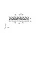
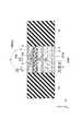
図1は、本発明に係る磁気デバイス30を備えた周波数検出器100の斜視図である。なお、図1においては、図面の見易さのため、後述のシリコン基板10、離間層16及び保護層22の図示を省略している(図2参照)。 FIG. 1 is a perspective view of a
磁気デバイス30は、磁気抵抗効果素子14と、磁気抵抗効果素子14に静磁界を印加するように設けられた磁界印加部としての一対のバイアス磁界印加層18と、磁気抵抗効果素子14の両端間に交流信号iを供給する一対の入力端子INPUT1,INPUT2と、磁気抵抗効果素子14の両端間出力電圧Vを取り出す一対の出力端子OUTPUT1,OUTPUT2とを備えている。なお、入力端子INPUT2及び出力端子OUTPUT2は、基準端子VREFであり、グランドに接続されている。 The
磁気抵抗効果素子14の積層方向をZ軸方向とし、これに直交する2軸をそれぞれX軸及びY軸とする。磁気抵抗効果素子14に対して、磁気抵抗効果素子14の膜面方向(XY平面方向)の一つであるX軸方向に離間した位置に、磁気抵抗効果素子14を挟むように一対のバイアス磁界印加層18が設けられている。磁気抵抗効果素子14のZ軸方向の両端には、それぞれ上部電極層20及び下部電極層12が接触し、磁気抵抗効果素子14に電気的に接続されている。上部電極層20及び下部電極層12は、突部を有する板状の電極であり、それぞれの突部間に磁気抵抗効果素子14が配置されている。なお、上部及び下部なる用語は、それぞれZ軸の正側の位置及び負側の位置を意味するものであり、重力の方向とは無関係である。 The stacking direction of the
上部電極層20及び下部電極層12には、それぞれ一対の上部電極層用パッド28及び下部電極層用パッド24が電気的に接続されている。なお、上部電極層用パッド28及び下部電極層用パッド24の一部は、それぞれ保護層22(図1においては図示せず。図2参照)内に埋設されているが、図1においては、上部電極層用パッド28及び下部電極層用パッド24のうち、保護層22内に埋設されている部分を破線で示している。 A pair of upper
一方の上部電極層用パッド28と一方の下部電極層用パッド24間には、入力端子INPUT1,INPUT2を介して信号源Sから交流信号iが印加される。即ち、交流信号iは、磁気抵抗効果素子14内をその積層方向に流れる。また、一方の上部電極層用パッド28と一方の下部電極層用パッド24間に直流が印加されないように、一方の入力端子INPUT1と一方の上部電極層用パッド28との間の配線には、キャパシタCが直列に挿入されている。 An AC signal i is applied from the signal source S between the one upper
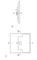
図2は、図1におけるII−II線に沿った磁気デバイス30の端面図である。図2に示すように、下部電極層12、磁気抵抗効果素子14及び上部電極層20は、この順にシリコン基板10上に積層されている。また、一対のバイアス磁界印加層18は、磁気抵抗効果素子14に対して、X軸方向に離間した位置に磁気抵抗効果素子14を挟むように設けられている。そして、一対のバイアス磁界印加層18と磁気抵抗効果素子14との間、及び一対のバイアス磁界印加層18と下部電極層12との間には、絶縁体からなる離間層16が設けられている。これにより、上部電極層20と下部電極層12とは、電気的には磁気抵抗効果素子14のみを介して接続されている。さらに、上部電極層20、一対のバイアス磁界印加層18及び離間層16を覆うように、保護層22が形成されている。 FIG. 2 is an end view of the
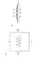
図3、図5及び図6を用いて、磁気抵抗効果素子14、離間層16及び一対のバイアス磁界印加層18の詳細について説明する。図3は、図2の磁気抵抗効果素子14付近の拡大端面図であり、図5は図3のV−V線に沿った磁気抵抗効果素子14の端面図であり、図6は図3のVI−VI線に沿った磁気抵抗効果素子14の端面図である。 The details of the
図3に示すように、磁気抵抗効果素子14は、磁化固定層3、磁化自由層5、及び磁化固定層3と磁化自由層5とに挟まれた非磁性層4を有している。具体的には、磁気抵抗効果素子14は、下地層1と、反強磁性層2と、反強磁性層2と交換結合して磁化の向き3AMがY軸の正方向に固定された下部強磁性層3Aと、Ruなどの導電性金属からなる非磁性中間層3Bと、非磁性中間層3Bを介して磁化の向き3CMが下部強磁性層3Aの磁化の向き3AMと反対向き(Y軸の負方向)に固定された上部強磁性層3Cと、非磁性層4と、強磁性体からなる磁化自由層5と、キャップ層9とがこの順に積層された構成を有している。ここで、下部強磁性層3Aと非磁性中間層3Bと上部強磁性層3Cとで磁化固定層3となるが、磁化固定層3の磁化の向きとは、磁化固定層3の2つの強磁性層のうち磁化自由層5に近い方である上部強磁性層3Cの磁化の向き3CMを意味するものとする。なお、磁気抵抗効果素子14は、下地層1又は/及びキャップ層9を有していなくてもよい。 As shown in FIG. 3, the
強磁性とは、隣り合うスピンが同一の方向を向いて整列し、全体として大きな磁気モーメントを持つ物質の磁性であり、強磁性体は外部磁場が無い場合においても自発磁化を有する。室温で強磁性を示す物質としては、Fe、Co、Ni及びGdがある。下部強磁性層3A、上部強磁性層3C、及び磁化自由層5を構成する強磁性体としては、例えば、Co、NiFe合金、CoFe合金等を用いることができるが、下部強磁性層3A、上部強磁性層3C、及び磁化自由層5のうちの少なくとも一つは、ハーフメタルで構成された層であることが好ましい。ハーフメタルとしては、例えば、Co2MnSi等のホイスラー合金、CrAsやCrSb等の閃亜鉛鉱型化合物、及びLa0.7Sr0.3MnO3等のペロブスカイト型Mn酸化物等を用いることができる。ホイスラー合金としては、X2YZ(ただし、XはFe,Co及びNiのいずれか、YはV,Cr及びMnのいずれか、ZはAl,Si,Ga,Ge及びSnのいずれか)で表される合金が好適である。また、ハーフメタルとして、規則構造であるL21又はB2構造のホイスラー合金はキュリー温度が室温以上であるため実用化の観点から好適である。Ferromagnetism is the magnetism of a substance that has adjacent spins aligned in the same direction and has a large magnetic moment as a whole, and a ferromagnetic material has spontaneous magnetization even in the absence of an external magnetic field. Materials that exhibit ferromagnetism at room temperature include Fe, Co, Ni, and Gd. As the ferromagnetic material constituting the lower
ハーフメタルとは、スピン分極率が略100%となる材料である。図4に通常の強磁性材料(CoFe合金等)の状態密度図(図4(A))、及びハーフメタルの状態密度図(図4(B))を示す。図4において、縦軸はエネルギー、横軸は電子の状態密度を表しており、縦軸よりも左側にアップスピンの状態密度を、縦軸よりも右側にダウンスピンの状態密度を表している。通常の強磁性材料の場合、図4(A)に示すように、フェルミ準位Ef近傍におけるアップスピンの状態密度Dupとダウンスピンの状態密度Ddownに差がある。そのため、P=(Dup−Ddown)/(Dup+Ddown)×100[%]で定義されるスピン分極率Pは、0<P<100[%]となる。一方、ハーフメタルの場合、図4(B)に示すように、フェルミ準位Ef近傍において、アップスピンのみが状態密度Dupを有し、ダウンスピンは状態密度を有していない。そのため、上記のように定義されるスピン分極率Pは100[%]となる。 Half metal is a material having a spin polarizability of approximately 100%. FIG. 4 shows a state density diagram (FIG. 4A) of a normal ferromagnetic material (CoFe alloy or the like) and a state density diagram of a half metal (FIG. 4B). In FIG. 4, the vertical axis represents energy, the horizontal axis represents the density of states of electrons, the upspin state density on the left side of the vertical axis, and the downspin state density on the right side of the vertical axis. In the case of a normal ferromagnetic material, as shown in FIG. 4A, there is a difference between the up-spin state density Dup and the down-spin state density Ddown in the vicinity of the Fermi level Ef. Therefore, the spin polarizability P defined by P = (Dup−Ddown) / (Dup + Ddown) × 100 [%] is 0 <P <100 [%]. On the other hand, in the case of the half metal, as shown in FIG. 4B, only the up spin has a density of states Dup and the down spin has no density of states in the vicinity of the Fermi level Ef. Therefore, the spin polarizability P defined as described above is 100 [%].
反強磁性層2を構成する反強磁性体としては、FeMn、IrMn、PtMn、NiMn等を用いることができる。As the antiferromagnetic material constituting the
また、磁化自由層5の膜厚は、例えば1〜10nmとすることができ、磁気抵抗効果素子14全体の膜厚は、例えば10〜100nmとすることができる。 The film thickness of the magnetization
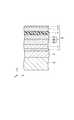
また、図3及び図5に示すように、非磁性層4は導電体からなる複数の電流狭窄層部4aと、絶縁体からなる絶縁層部4bとで構成されている。そして、電流狭窄層部4aは、絶縁層部4bをその膜厚方向(Z軸に沿った方向)に貫通している。そのため、磁気抵抗効果素子14内をその積層方向に流れる交流信号i(図1参照)は、非磁性層4を通過する際、絶縁層部4bを通過することはできず、電流狭窄層部4aのみを通過する。そのため、磁気抵抗効果素子14の非磁性層4が全て導電性金属で形成されている場合と比較して、即ち磁気抵抗効果素子14が通常のCPP(Current Perpendicular to Plane)型のGMR素子である場合と比較して、非磁性層4を通過する電流の経路は電流狭窄層部4aが形成された特定の領域に制限されている。この電流狭窄層部4aは、その膜厚方向(Z軸に沿った方向)と垂直な面(XY平面)についての一つの断面積4aSが0.00001〜0.01μm2であることが好ましい。また、非磁性層4の膜厚は、例えば0.5〜3nmとすることができる。電流狭窄層部4aを構成する材料としては、例えばCu、Au、Ag、Ruを用いることができ、絶縁層部4bを構成する材料としては、例えばAl2O3、SiO2、TiO2、HfO2、MgOを用いることができる。As shown in FIGS. 3 and 5, the
また、図3に示すように、磁気抵抗効果素子14に対してX軸方向に離間した位置に、磁化自由層5を挟むように磁界印加部としての一対のバイアス磁界印加層18が設けられている。バイアス磁界印加層は、CoCrPt等の硬磁性材料で構成されており、その残留磁化18M1の方向が図3のX軸方向に向くように着磁されている。そのため、バイアス磁界印加層18は、自発的に静磁界18M2を図3のX軸方向に発生し、この静磁界18M2はバイアス磁界として磁化自由層5に印加される。その結果、磁化自由層5の磁化の方向5Mは、静磁界18M2の磁化自由層5内における向き、即ち、X軸の方向を向くことになる。また、バイアス磁界印加層18の厚さは、後述するように共振周波数f0が所定の値になるように調整されるが、例えば1〜100nmとすることができる。Further, as shown in FIG. 3, a pair of bias magnetic field application layers 18 as magnetic field application parts are provided so as to sandwich the magnetization
また、図6に示すように、静磁界18M2の磁化自由層5内における向きと、磁化固定層3の磁化方向3CMとが磁化固定層3の膜面内において成す角度θは、本実施形態の場合90度となっている。この角度θは、90度以外の角度であってもよいが、後述のように磁化自由層5の磁化の向き5Mを容易に振動させる観点から、この角度θは5度以上であることが好ましい。 In addition, as shown in FIG. 6, the angle θ formed by the direction of the static magnetic field 18M2 in the magnetization
次に、磁気デバイス及び周波数検出器の動作について、図1〜図3を用いて説明する。 Next, operations of the magnetic device and the frequency detector will be described with reference to FIGS.
交流信号iを磁気抵抗効果素子14に供給すると、磁気抵抗効果素子14の磁化自由層5内に特定の極性のスピンが注入され、この注入量に応じて、磁化自由層5の磁化の向き5Mが変化する。磁化自由層5の磁化の向き5Mは、交流信号iが供給されていないときには、バイアス磁界印加層18から発生する静磁界18M2の磁化自由層5内での方向に一致している。磁気抵抗効果素子14の磁化固定層3側から磁化自由層5に偏極スピンが注入される場合、上部強磁性層3Cの磁化の向き3CMに、その磁化の向きが揃う向きの極性のスピンが磁化自由層5に注入され、磁化自由層5は、磁化自由層5の磁化の向き5Mを上部強磁性層3Cの磁化の向き3CMと平行になる方向に回転させるようなトルクを受ける。これとは逆向きに磁化自由層5に電子を注入した場合には、上部強磁性層3Cの磁化の向き3CMに揃った極性のスピンは磁化自由層5内には注入されないので、上記とは逆の極性のスピンが磁化自由層5に注入され、磁化自由層5は、磁化自由層5の磁化の向き5Mを上部強磁性層3Cの磁化の向き3CMと反平行になる方向に回転させるようなトルクを受ける。 When the AC signal i is supplied to the
交流信号iの極性は時間と共に変化するので、磁化自由層5の磁化の向き5Mは、交流信号iの大きさと周波数に影響を受けて振動する。磁気抵抗効果素子14の磁化自由層5の磁化の向き5Mの固有振動数fFと、磁気抵抗効果素子14を流れる交流信号iの周波数fが一致した場合(f0=fF=f)、磁化自由層5の磁化の向き5Mの振動が共振する。この際、磁気抵抗効果素子14の抵抗値は磁化自由層5の磁化の向き5Mと磁化固定層3の磁化の向き3CMの相対的な角度に依存する。その結果、磁気抵抗効果素子14の素子の抵抗値はその周波数で急激に変動することとなり、交流信号iの電圧が変動して直流成分を有し、他方の上部電極層用パッド28と他方の下部電極層用パッド24にそれぞれ接続された出力端子OUTPUT1,OUTPUT2の間の電圧Vとして出力される。Since the polarity of the AC signal i changes with time, the
共振周波数f0(固有振動数fF)は、磁気抵抗効果素子14の磁化自由層5に印加される静磁界18M2の大きさに依存し、静磁界18M2が大きくなるに従って上昇する。この静磁界18M2の大きさは、バイアス磁界印加層18の材質、膜厚等に依存する。これらの条件を調節して静磁界18M2の大きさを増大させると(18M2a<18M2b<18M2c)、共振(共鳴)周波数f0が上昇する(図7参照)。すなわち、バイアス磁界印加層18の材質、膜厚等に依存して共振周波数f0が決定され、入力された交流信号iのうち、決定された共振周波数f0の成分に対応する電圧Vが選択的に変動して直流成分を有し、出力端子OUTPUT1,OUTPUT2の間に現れる(図8参照)。The resonance frequency f0 (natural frequency fF ) depends on the magnitude of the static magnetic field 18M2 applied to the magnetization
また、本実施形態の周波数検出器100は、磁気デバイス30を備えており、出力端子OUTPUT1,OUTPUT2から出力される電圧Vをモニタするモニタ回路40を更に備えている。交流信号iを磁気抵抗効果素子14に供給すると、磁化自由層5の固有振動数fFに対応した特定の共振周波数f0の電圧Vがモニタ回路40によって検出される(図8参照)。すなわち、本実施形態の周波数検出器100は交流信号iに含まれる特定の周波数を検出する周波数検出器として機能する。Further, the
また、周波数検出器100は、モニタ回路40と磁気抵抗効果素子14との間に介在するローパスフィルタLを更に備えている。これは、磁気抵抗効果素子14の両端間には、一対の入力端子INPUT1,INPUT2と、一対の出力端子OUTPUT1,OUTPUT2が接続されているが、入力端子INPUT1,INPUT2には交流信号iが印加されているため、出力端子OUTPUT1,OUTPUT2から磁化自由層5の磁化の向き5Mの固有振動数fFに対応した特定の周波数の信号電圧の直流電圧のみを選択的に取り出すためである。ローパスフィルタLは、磁気抵抗効果素子14からの直流成分のみを透過させてモニタ回路40に入力させる。本実施形態においては、ローパスフィルタLは、上部電極層用パッド28と出力端子OUTPUT1との間に介在するコイルから構成されている。The
次に、本実施形態に係る磁気デバイス30の製造方法を、図9〜図19を用いて説明する。図9〜図15の(A)は磁気デバイス30の中間体の平面図である。また、図9〜図14の(B)及び図15の(B)(C)は、各図の平面図(A)における所定の線に沿った磁気デバイス30の中間体の端面図である。 Next, a method for manufacturing the
まず、図9に示すように、シリコン基板10上に所定形状にパターニングされたCu等の導電性材料からなる下部電極層12を形成し、全面に磁気抵抗効果素子14を形成し、将来磁気抵抗効果素子14を残す部分にパターニングされたレジストマスク15を形成する。ここで、下部電極層12及び磁気抵抗効果素子14は、例えばスパッタリング装置を用いて成膜することができる。磁気抵抗効果素子14の形成方法の詳細は、後述する。 First, as shown in FIG. 9, a
続いて、図10に示すように、磁気抵抗効果素子14のうちレジストマスク15によってマスクされていない部分を、イオンミリング等によって除去する。これにより、磁気抵抗効果素子14のパターンが形成される。 Subsequently, as shown in FIG. 10, a portion of the
次に、図11に示すように、磁気抵抗効果素子14の側面と、下部電極層12とシリコン基板10の露出表面に、SiO2等からなる離間層16を形成した後、磁気抵抗効果素子14の両側面に磁気抵抗効果素子14と離間するようにパターニングされた一対のバイアス磁界印加層18を形成する。ここで、離間層16は、例えばSi(OC2H5)4を用いたCVD装置によって形成することができる。Next, as shown in FIG. 11, a
そして、図12に示すように、Ta等からなる保護層22aを全面に成膜した後、磁気抵抗効果素子14及びバイアス磁界印加層18が露出するまでCMP等によって表面をラッピングすることにより、凹部に保護層22aを埋め、全面を平坦にする。 Then, as shown in FIG. 12, a
続いて、図13に示すように、所定形状にパターニングされたCu等の導電性材料からなる上部電極層20を、磁気抵抗効果素子14と電気的に接触するように形成する。 Subsequently, as shown in FIG. 13, an
次に、図14に示すように、全体にSiO2等からなる保護層22bを形成した後に、表面をCMP等によってラッピングして平坦化する。Next, as shown in FIG. 14, after a
そして、図15に示すように、保護層22(=保護層22a+保護層22b)の表面の将来上部電極層用パッド28及び下部電極層用パッド24を形成する領域以外をレジストでマスクし、マスクされていない領域の保護層22を、例えばC4F8等を用いた反応性イオンエッチング装置等によって除去して上部電極層20及び下部電極層12に達するスルーホールを形成し、このスルーホール内にスパッタ装置等によってAu等の導電性材料を成膜して一対の上部電極層用パッド28及び下部電極層用パッド24を形成する。Then, as shown in FIG. 15, the surface of the protective layer 22 (=
そして、図1に示すように、一対の上部電極層用パッド28及び下部電極層用パッド24の一方に一対の入力端子INPUT1,INPUT2を接続し、一対の上部電極層用パッド28及び下部電極層用パッド24の他方に一対の出力端子OUTPUT1,OUTPUT2を接続することにより、磁気デバイス30が完成する。 As shown in FIG. 1, a pair of input terminals INPUT1 and INPUT2 are connected to one of a pair of upper
次に、磁気抵抗効果素子14の形成方法の詳細について、図16〜図19を用いて説明する。 Next, details of a method of forming the
まず、図16に示すように、シリコン基板10上に形成された下部電極層12上に、例えばスパッタリング法によって、Ta、Ta/NiFe、又はNiCr等からなる下地層1と、FeMn、IrMn、PtMn、又はNiMn等からなる反強磁性層2と、Co、NiFe合金、CoFe合金やハーフメタルからなる下部強磁性層3Aと、Ru等からなる非磁性中間層3Bと、下部強磁性層3Aと同様の材料からなる上部強磁性層3Cと、酸化され易さの異なる2種類の金属(例えば、CuとAl)からなる合金層4Xをこの順に形成する。この合金層4Xは、スパッタリング法を用いる場合、2種類の金属の合金ターゲットを用いて形成してもよいし、2種類の金属についての別個のターゲットを用いて同時スパッタリングによって形成してもよい。 First, as shown in FIG. 16, an
次に、図17に示すように、合金層4Xを構成する金属のうち酸化され易い金属(例えば、Al)のみを選択的に酸化させることにより、Cu等の導電体からなる複数の電流狭窄層部4aと、Al2O3等の絶縁体からなる絶縁層部4bとからなる非磁性層4を形成する。この選択的な酸化は、例えば、スパッタリング法によって合金層4Xを形成した後に、成膜チャンバー内に所定流量の酸素を所定時間導入して自然酸化を行うことによって実現することができる。また、この自然酸化は、合金層4XにArイオンを照射しながら行うことが好ましい。これにより、酸化されにくい金属(例えばCu)の一部が酸化されてしまった場合においても、酸化された金属をArイオンビームによって還元し、金属状態に戻すことが可能となる。このようにして、絶縁層部4bと、絶縁層部4bをその膜厚方向に貫通する電流狭窄層部4aとからなる非磁性層4が形成される。このような方法で発明者らが非磁性層4を形成したところ、電流狭窄層部4aの一つの断面積4aS(図5参照)を、1.0×10⁻⁴μm2とすることができた。Next, as shown in FIG. 17, a plurality of current confinement layers made of a conductor such as Cu are selectively oxidized by selectively oxidizing only a metal (for example, Al) that is easily oxidized among the metals constituting the
次に、図18に示すように、非磁性層4上に、Co−Fe合金やNi−Fe合金等、或いはこれらの積層体等からなる磁化自由層5と、Ta等からなるキャップ層9を順次形成する。このようにして、磁気抵抗効果素子14が形成される。 Next, as shown in FIG. 18, on the
続いて、磁気抵抗効果素子14に対して、図18のY軸の正方向に磁場を印加しながら、アニール処理を行う。このアニール処理における最高到達温度は、反強磁性層2のブロッキング温度程度とする。すると、図19に示すように、下部強磁性層3Aと反強磁性層2は交換結合し、下部強磁性層3Aの磁化の向き3AMはアニール処理時の磁場印加方向であるY軸の正方向に固定される。そして、上部強磁性層3Cの磁化の向き3CMは、非磁性中間層3Bを介して下部強磁性層3Aの磁化の向き3AMと反対向き(Y軸の負方向)に固定される。また、その後、X軸方向に磁場を印加しながらアニール処理を行い、磁化自由層5の磁化容易軸をX軸方向に設定するのが好ましい。この際、磁化固定層3の磁化方向3CMを変化させないように、上述の磁化固定層3の磁化方向3CMの固定のためのアニール処理の場合と比較して、印加磁場を弱く、加熱温度を低くするのが好ましい。なお、これらのアニール処理を行うのは、磁気抵抗効果素子14の形成直後でなくてもよい。例えば、保護層22を形成した後にこれらのアニール処理を行ってもよい(図14参照)。 Subsequently, annealing is performed on the
上述のような本実施形態に係る磁気デバイス30及び周波数検出器100によってスピンデバイスの共振を用いれば、通常のSi半導体技術では得られないGHz帯の周波数解析を行うことができるため、通信技術の更なる発展を期待することができる。 If the resonance of the spin device is used by the
また、本実施形態に係る磁気デバイス30では、入力された交流信号iの電流は、磁気抵抗効果素子14の非磁性層14を通過する際、非磁性層14の絶縁層部14bを通過することはできず、電流狭窄層部14aのみを通過することとなる(図3参照)。磁気抵抗効果素子14の非磁性層14をこのような構成にすることにより、磁気デバイス30の出力直流電圧のピークの半値幅が十分に小さくなることを発明者らは新たに見出した。このような現象について、推測される原理を図20を用いて説明する。 In the
図20(A)は、従来の磁気デバイスの磁気抵抗効果素子が有する非磁性層近傍の断面図であり、図20(B)は、本実施形態に係る磁気デバイスの磁気抵抗効果素子が有する非磁性層近傍の断面図である。図20(A)に示すように、従来の磁気デバイスの磁気抵抗効果素子が有する非磁性層4Cは、Cu等の導電性材料のみで形成されている。そのため、上部強磁性層3Cから磁化自由層5に向かって電子eが移動する際、電子eは、非磁性層4Cの全体を通過することになる。そして、磁化自由層5に到達した電子eは、磁化自由層5の磁化と相互作用して、磁化自由層5内に磁化の共振5hを多数生じさせる。その際、電子eは非磁性層4Cの全体を通過しているため、磁化自由層5内の比較的広い領域の磁化を共振させる電子eと、磁化自由層5内の比較的狭い領域の磁化を共振させる電子eがある。その結果、磁化自由層5内に生じた磁化の共振5hの共振の大きさはばらつくことになり、これが原因で磁気デバイスの出力直流電圧のピーク形状が鈍くなると考えられる。 FIG. 20A is a cross-sectional view of the vicinity of the nonmagnetic layer of the magnetoresistive effect element of the conventional magnetic device, and FIG. It is sectional drawing of the magnetic layer vicinity. As shown in FIG. 20A, the
それに対して、図20(B)に示すように、本実施形態に係る磁気デバイス30の磁気抵抗効果素子14が有する非磁性層4は、絶縁体からなる絶縁層部4bと、絶縁層部4bをその膜厚方向に貫通する電流狭窄層部4aとで構成されている。そのため、上部強磁性層3Cから磁化自由層5に向かって電子eが移動する際、電子eは、非磁性層4の電流狭窄層部4a内のみを通過する。そして、磁化自由層5に到達した電子eは、磁化自由層5の磁化と相互作用して、磁化自由層5内に磁化の共振5hを多数生じさせる。その際、電子eは非磁性層4の電流狭窄層部4a内のみを通過しているため、磁化自由層5内の電流狭窄層部4a近傍の領域の磁化のみが電子eによって共振する。そのため、共振する磁化自由層5内の領域の大きさのばらつきは従来と比較して小さくなる。その結果、磁化自由層5内に生じた磁化の共振5hの共振の大きさのばらつきは抑制され、磁気デバイスの出力直流電圧のピーク形状は鋭くなると考えられる。 On the other hand, as shown in FIG. 20B, the
さらに、本実施形態に係る磁気デバイス30は、磁化自由層5に静磁界18M2を印加するように設けられた磁界印加部としての一対のバイアス磁界印加層18を備えている(図3参照)。そのため、磁化自由層5の材料や膜厚等を適切に選択すれば、磁化自由層5に所定の大きさの静磁場18M2を印加することができる。そして、磁化自由層5の磁化の向き5Mの固有振動数fF(共振周波数f0)は、磁化自由層5に印加される静磁場5Mの大きさに依存して決定される。そのため、入力された交流信号i(図1参照)のうち、決定された共振周波数f0の成分に対応する特定の周波数の信号の電圧を選択的に変動させて直流成分を出力することが可能な磁気デバイス30となっている。Furthermore, the
さらに、本実施形態の係る磁気デバイス30は、電流狭窄部4aのその膜厚方向と垂直な面についての一つの断面積4aSが、好ましくは、0.00001〜0.01μm2としている(図3、図5参照)。このため、磁気デバイス30の出力直流電圧のピークの半値幅が特に小さくなっている。Furthermore, in the
さらに、本実施形態の係る磁気デバイス30は、好ましくは下部強磁性層3A、上部強磁性層3C、及び磁化自由層5のうちの少なくとも一つは、ハーフメタルで構成された層
としている(図3参照)。 そのため、磁気デバイス30の出力直流電圧を増大させることができる。即ち、ホイスラー合金等のハーフメタルは室温でのスピン分極率が略100%であるため、磁気抵抗効果素子14の磁気抵抗効果率が増大する。そのため、磁化自由層5の磁化の向き5Mが磁気抵抗効果素子14を流れる交流信号iと共振した際、磁気抵抗効果素子14の抵抗値はその周波数でさらに急激に変動することとなる。その結果、磁気デバイス30の出力直流電圧は増大することとなる。Furthermore, in the
さらに、本実施形態に係る磁気デバイス30は、交流信号iが含む周波数成分のうち、磁化自由層5の磁化の向き5Mの固有振動数fFに対応する周波数成分と、磁化自由層5の磁化の向き5Mとが共振し、固有振動数fFに対応する周波数成分を変動させて直流電圧を出力している。そのため、磁化自由層5の固有振動数fFが所定の大きさになるように磁気デバイス30を製造すれば、交流信号iが含む周波数成分のうちの所定の周波数成分を選択的に変動させて直流電圧を出力することが可能な磁気デバイス30とすることができる。Furthermore, the
また、本実施形態の周波数検出器100は、上述の磁気デバイス30と、一対の出力端子OUTPUT1,OUTPUT2から出力される電圧をモニタするモニタ回路40とを備えている(図1参照)。このため、入力された交流信号iのうち、特定の周波数の信号の電圧がモニタ回路40によって検出されるような周波数検出器100が実現されている。 Further, the
また、本実施形態の周波数検出器100は、モニタ回路40と磁気抵抗効果素子14との間に介在するローパスフィルタLを更に備えている(図1参照)。このため、磁気抵抗効果素子14からの直流成分のみを透過させてモニタ回路40に入力させることができる。即ち、磁気抵抗効果素子14の両端間には交流信号iが印加されているため、ローパスフィルタLを設けることにより、交流信号iのうち選択的に変動した特定の周波数の信号の直流電圧のみを取り出すことが可能となっている。 Further, the
以下、本発明の効果をより一層明らかなものとするため、実施例および比較例を用いて説明する。図21〜図24は実施例1〜4に係る磁気デバイスに関して入力信号の周波数対出力電圧の関係を示す図である。また、図25は比較例1に係る磁気デバイスに関して入力信号の周波数対出力電圧の関係を示す図である。 Hereinafter, in order to further clarify the effects of the present invention, description will be made using examples and comparative examples. FIGS. 21 to 24 are diagrams illustrating the relationship between the frequency of the input signal and the output voltage for the magnetic devices according to the first to fourth embodiments. FIG. 25 is a diagram showing the relationship between the frequency of the input signal and the output voltage with respect to the magnetic device according to Comparative Example 1.
実施例1〜4に係る磁気デバイスについては、磁気抵抗効果素子が有する非磁性層を、絶縁体からなる絶縁層部4bと、絶縁層部4bをその膜厚方向に貫通する電流狭窄層部4aとで構成した(図3、図5参照)。また、実施例1及び実施例2に係る磁気デバイスについては、下部強磁性層3A、上部強磁性層3C、及び磁化自由層5を構成する強磁性体として、ハーフメタル以外の強磁性体を用いた。また、実施例1及び実施例2は、非磁性層4の製造方法、特に電流狭窄部4aの形成方法の点において相違する。実施例1に係る磁気デバイスは、上述の実施形態における製造方法により非磁性層4を形成し(図16及び図17参照)、導電性狭窄部4aの断面積4aS(図5参照)は約0.00003μm2となった。For the magnetic devices according to Examples 1 to 4, the nonmagnetic layer included in the magnetoresistive effect element includes an insulating
一方、実施例2に係る磁気デバイスは、非磁性層4を次の製造方法を用いて形成した。即ち、まず、磁化固定層3上に、例えばSi(OC2H5)4を用いたCVD装置によってSiO2層を形成した(図17参照)。そして、電流狭窄層部4a形成予定領域に開口を有するレジストパターンをSiO2層上に形成し、例えばC4F8ガスを用いた反応性イオンエッチング装置によってマスクされていない領域のSiO2層を除去した。そして、スパッタ装置等によってCu等の導電性金属を成膜し、CMP装置等によってSiO2層が露出するまで表面を平坦化することにより、図17に示されるような電流狭窄層部4a及び絶縁層部4bからなる非磁性層4を形成した。このような方法で発明者らが非磁性層4を形成したところ、電流狭窄層部4aの厚さ方向に垂直な一つの断面積4aS(図5参照)は、0.004μm2となった。On the other hand, in the magnetic device according to Example 2, the
また、実施例3は、固定層3の上部磁性層3Cを形成する材料として、ハーフメタルであるCo2MnGeを用いたものである。その他の構成は、実施例1と同一である。また、比較例1は、非磁性層をCuのみで形成したものであり、その他の構成は、実施例1と同一である。In Example 3, Co2 MnGe, which is a half metal, is used as a material for forming the upper
図21に示すように、実施例1の出力電圧は、入力信号の周波数に対して鋭いピーク形状を示した。そして、出力電圧の最大値は、51μVとなり、出力電圧のピークの半値幅は0.30[GHz]となった。また、図22に示すように、実施例2の出力電圧は、入力信号の周波数に対して鋭いピーク形状を示した。そして、出力電圧の最大値は、57μVとなり、出力電圧のピークの半値幅は0.55[GHz]となった。 As shown in FIG. 21, the output voltage of Example 1 showed a sharp peak shape with respect to the frequency of the input signal. The maximum value of the output voltage was 51 μV, and the half width of the peak of the output voltage was 0.30 [GHz]. Also, as shown in FIG. 22, the output voltage of Example 2 showed a sharp peak shape with respect to the frequency of the input signal. The maximum value of the output voltage was 57 μV, and the half width of the peak of the output voltage was 0.55 [GHz].
また、図23に示すように、実施例3の出力電圧は、入力信号の周波数に対して鋭いピーク形状を示した。そして、出力電圧の最大値は、150μVとなり、出力電圧のピークの半値幅は0.28[GHz]となった。実施例3においては、上述のように、出力電圧のピークが鋭くなったのに加え、出力電圧の最大値が大きくなった。 Moreover, as shown in FIG. 23, the output voltage of Example 3 showed a sharp peak shape with respect to the frequency of the input signal. The maximum value of the output voltage was 150 μV, and the half width of the peak of the output voltage was 0.28 [GHz]. In Example 3, the peak value of the output voltage became sharper as described above, and the maximum value of the output voltage was increased.
一方、図24に示すように、比較例1の出力電圧は、入力信号の周波数に対して緩やかなピーク形状を示した。そして、出力電圧の最大値は、50μVとなり、出力電圧のピークの半値幅は1.30[GHz]となった。 On the other hand, as shown in FIG. 24, the output voltage of Comparative Example 1 showed a gradual peak shape with respect to the frequency of the input signal. The maximum value of the output voltage was 50 μV, and the half width of the peak of the output voltage was 1.30 [GHz].
本発明は上記実施形態に限定されるものではなく、様々な変形態様が可能である。 The present invention is not limited to the above embodiment, and various modifications can be made.
例えば、上述の実施形態においては、磁界印加部としての一対のバイアス磁界印加層18が磁気抵抗効果素子14の両側面に設けられているが(図3参照)、磁界印加部はこのような態様に限られない。例えば、バイアス磁界印加層18の代わりに、磁気抵抗効果素子14内において、磁化自由層5上に非磁性層を介して硬磁性層を設けてもよい。この場合、硬磁性層が磁界印加部となり、そこから発生する静磁界が磁化自由層5に印加される。また、磁化自由層5上に非磁性層を介して、又は直接反強磁性層を設けてもよい。この場合、反強磁性層が磁界印加部となり、そこから発生する交換結合磁界が磁化自由層5に印加される。 For example, in the above-described embodiment, a pair of bias magnetic field application layers 18 as magnetic field application units are provided on both side surfaces of the magnetoresistive effect element 14 (see FIG. 3). Not limited to. For example, instead of the bias magnetic
さらに、磁界印加部の別の態様として、図25に示すような構成も可能である。即ち、磁気抵抗効果素子14に近接して、磁界印加部としての電流磁界発生部18aを設けることも可能である。電流磁界発生部は、図25のY軸方向に沿って延びる導電体で形成されており、これに電流を流すことによって電流磁界18M2が発生し、この電流磁界18M2が磁化自由層5に印加される。 Furthermore, as another aspect of the magnetic field application unit, a configuration as shown in FIG. 25 is possible. That is, it is possible to provide a current
なお、磁界印加部を特に設けない構成であっても、本発明の実施は可能である。 Note that the present invention can be implemented even if the magnetic field application unit is not particularly provided.
また、上述の実施形態においては、磁気抵抗効果素子14の磁化固定層3及び磁化自由層5の間には非磁性層として非磁性層4のみが設けられているが、非磁性層4と磁化固定層3との間、又は/及び非磁性層4と磁化自由層5との間にさらにCu層等の非磁性層を設けてもよい。 In the above-described embodiment, only the
また、上述の実施形態においては、磁化固定層3を下部強磁性層3A、非磁性中間層3B、及び上部強磁性層3Cによって構成しているが、磁化固定層3は上部強磁性層3Cのみで構成してもよい。 In the above-described embodiment, the fixed
また、交流信号を発生させるための信号発生装置を信号源Sとしてさらに備える構成も可能である。これにより、信号発生装置から発生する信号を処理する磁気デバイスを得ることができる。信号発生装置としてVCO(Voltage Controlled Oscillator)を用いれば、送信機として用いることができる。また、信号発生装置としてアンテナを用いることもできる。この場合、アンテナで受信した信号を処理する磁気デバイスを得ることができる。 Moreover, the structure further provided as the signal source S with the signal generator for generating an alternating current signal is also possible. Thereby, the magnetic device which processes the signal which generate | occur | produces from a signal generator can be obtained. If a VCO (Voltage Controlled Oscillator) is used as the signal generator, it can be used as a transmitter. An antenna can also be used as the signal generator. In this case, a magnetic device that processes a signal received by the antenna can be obtained.
また、図26に示すように、固有振動数fFがそれぞれ異なる複数の磁気抵抗効果素子30a、30b、30cと、複数の磁気抵抗効果素子30a、30b、30cから出力電圧を取り出すための複数の出力端子OUTPUT1a、OUTPUT2a、OUTPUT1b、OUTPUT2b、OUTPUT1c、OUTPUT2cとを備える周波数検出器100aも可能である。ここで、出力端子OUTPUT1a、OUTPUT1b及びOUTPUT1cは、それぞれ上述の実施形態における出力端子OUTPUT1に対応し、出力端子OUTPUT2a、OUTPUT2b及びOUTPUT2cは、それぞれ上述の実施形態における出力端子OUTPUT2に対応し、磁気デバイス30a、30b及び30cは、それぞれ上述の実施形態における磁気デバイス30に対応する(図1参照)。これにより、交流信号iが複数の周波数成分を含んでいる場合に、複数の固有振動数fFに対応した複数の周波数成分を変動させ、それに対応して複数の電圧Va、Vb、Vcをそれぞれ出力する周波数検出器100aを得ることができる。ここで、直流電圧Va、Vb及びVcは、上述の実施形態における出力電圧Vに対応し、周波数検出器100aは、上述の実施形態における周波数検出器100に対応する(図1参照)。Further, as shown in FIG. 26, a plurality of
3・・・磁化固定層、4・・・非磁性層、4a・・・電流狭窄層部、4b・・・絶縁層部、14・・・磁気抵抗効果素子、INPUT1,INPUT2・・・入力端子、OUTPUT1,OUTPUT2・・・出力端子。
DESCRIPTION OF
Claims (11)
Translated fromJapanese前記磁気抵抗効果素子に対して、その積層方向に交流信号を流すための入力端子と、
前記磁気抵抗効果素子から出力電圧を取り出すための出力端子と、
を備え、
前記非磁性層は、絶縁体からなる絶縁層部と、前記絶縁層部をその膜厚方向に貫通する導電体からなる電流狭窄層部と、を含むことを特徴とする磁気デバイス。A magnetoresistive element having a magnetization fixed layer, a magnetization free layer, and a nonmagnetic layer sandwiched between the magnetization fixed layer and the magnetization free layer;
For the magnetoresistive effect element, an input terminal for flowing an AC signal in the stacking direction;
An output terminal for extracting an output voltage from the magnetoresistive element;
With
The nonmagnetic layer includes an insulating layer portion made of an insulator, and a current confinement layer portion made of a conductor that penetrates the insulating layer portion in the film thickness direction.
前記固有振動数に対応する周波数成分を変動させて直流電圧を出力することを特徴とする請求項1〜5のいずれか一項に記載の磁気デバイス。Of the frequency components included in the AC signal, the frequency component corresponding to the natural frequency of the magnetization direction of the magnetization free layer resonates with the magnetization direction of the magnetization free layer,
The magnetic device according to claim 1, wherein a DC voltage is output by changing a frequency component corresponding to the natural frequency.
前記出力端子から出力される電圧をモニタするモニタ回路と、
を備えることを特徴とする周波数検出器。A magnetic device according to any one of claims 1 to 9,
A monitor circuit for monitoring the voltage output from the output terminal;
A frequency detector comprising:
Priority Applications (2)
| Application Number | Priority Date | Filing Date | Title |
|---|---|---|---|
| JP2007305010AJP2009130216A (en) | 2007-11-26 | 2007-11-26 | Magnetic device and frequency detector |
| US12/271,238US7825658B2 (en) | 2007-11-26 | 2008-11-14 | Magnetic device and frequency detector |
Applications Claiming Priority (1)
| Application Number | Priority Date | Filing Date | Title |
|---|---|---|---|
| JP2007305010AJP2009130216A (en) | 2007-11-26 | 2007-11-26 | Magnetic device and frequency detector |
Publications (1)
| Publication Number | Publication Date |
|---|---|
| JP2009130216Atrue JP2009130216A (en) | 2009-06-11 |
Family
ID=40675050
Family Applications (1)
| Application Number | Title | Priority Date | Filing Date |
|---|---|---|---|
| JP2007305010APendingJP2009130216A (en) | 2007-11-26 | 2007-11-26 | Magnetic device and frequency detector |
Country Status (2)
| Country | Link |
|---|---|
| US (1) | US7825658B2 (en) |
| JP (1) | JP2009130216A (en) |
Cited By (1)
| Publication number | Priority date | Publication date | Assignee | Title |
|---|---|---|---|---|
| JP2016092746A (en)* | 2014-11-11 | 2016-05-23 | Tdk株式会社 | Detector |
Families Citing this family (15)
| Publication number | Priority date | Publication date | Assignee | Title |
|---|---|---|---|---|
| JP4905402B2 (en)* | 2008-03-31 | 2012-03-28 | Tdk株式会社 | Mixer and frequency converter |
| JP5347718B2 (en)* | 2009-05-28 | 2013-11-20 | Tdk株式会社 | Mixer and frequency converter |
| DE102009030723A1 (en)* | 2009-06-26 | 2011-01-05 | Siemens Aktiengesellschaft | Magnetic field sensor with crossed magnetizations in reference and measuring layer |
| US8994370B2 (en)* | 2010-07-30 | 2015-03-31 | Peugeot Citroën Automobiles SA | Magnetoresistor integrated sensor for measuring voltage or current, and diagnostic system |
| US8421440B2 (en)* | 2010-10-25 | 2013-04-16 | Nokia Corporation | Apparatus for spectrum sensing and associated methods |
| JP5796431B2 (en) | 2011-09-16 | 2015-10-21 | Tdk株式会社 | Frequency converter |
| JP5790359B2 (en) | 2011-09-16 | 2015-10-07 | Tdk株式会社 | Mixer |
| JP5790360B2 (en) | 2011-09-16 | 2015-10-07 | Tdk株式会社 | Mixer with frequency selectivity |
| US9116197B2 (en)* | 2012-07-11 | 2015-08-25 | Wisconsin Alumni Research Foundation | Integrated interconnect and magnetic-field detector for current sensing |
| FR3014205B1 (en)* | 2013-12-04 | 2016-01-01 | Thales Sa | ANALOG SPECTRUM ANALYZER |
| CN103794224B (en)* | 2014-01-27 | 2017-01-11 | 华中科技大学 | Non-volatile logic device and logic operation method based on phase-change magnetic materials |
| US9966922B2 (en)* | 2016-05-25 | 2018-05-08 | Tdk Corporation | Magnetoresistive effect device |
| JP2019047030A (en) | 2017-09-05 | 2019-03-22 | Tdk株式会社 | Spin current magnetization reversal element, magnetoresistance effect element, magnetic memory, and high frequency magnetic element |
| US10741318B2 (en)* | 2017-09-05 | 2020-08-11 | Tdk Corporation | Spin current magnetization rotational element, spin-orbit-torque magnetoresistance effect element, magnetic memory, and high-frequency magnetic element |
| US10818990B2 (en)* | 2018-02-01 | 2020-10-27 | Tdk Corporation | Magnetoresistance effect device and magnetoresistance effect module |
Citations (4)
| Publication number | Priority date | Publication date | Assignee | Title |
|---|---|---|---|---|
| JP2006286855A (en)* | 2005-03-31 | 2006-10-19 | Toshiba Corp | Magnetic oscillation element, magnetic sensor, magnetic head, and magnetic reproducing apparatus |
| JP2006295908A (en)* | 2005-03-18 | 2006-10-26 | Japan Science & Technology Agency | Microwave transmission element integrated microwave generation element and microwave transmission circuit integrated microwave detection element |
| JP2007124340A (en)* | 2005-10-28 | 2007-05-17 | Toshiba Corp | High-frequency oscillation element, in-vehicle radar device using the same, inter-vehicle communication device, and inter-information terminal communication device |
| JP2009135471A (en)* | 2007-10-31 | 2009-06-18 | National Institute Of Advanced Industrial & Technology | Micro oscillation element and detection element |
- 2007
- 2007-11-26JPJP2007305010Apatent/JP2009130216A/enactivePending
- 2008
- 2008-11-14USUS12/271,238patent/US7825658B2/ennot_activeExpired - Fee Related
Patent Citations (4)
| Publication number | Priority date | Publication date | Assignee | Title |
|---|---|---|---|---|
| JP2006295908A (en)* | 2005-03-18 | 2006-10-26 | Japan Science & Technology Agency | Microwave transmission element integrated microwave generation element and microwave transmission circuit integrated microwave detection element |
| JP2006286855A (en)* | 2005-03-31 | 2006-10-19 | Toshiba Corp | Magnetic oscillation element, magnetic sensor, magnetic head, and magnetic reproducing apparatus |
| JP2007124340A (en)* | 2005-10-28 | 2007-05-17 | Toshiba Corp | High-frequency oscillation element, in-vehicle radar device using the same, inter-vehicle communication device, and inter-information terminal communication device |
| JP2009135471A (en)* | 2007-10-31 | 2009-06-18 | National Institute Of Advanced Industrial & Technology | Micro oscillation element and detection element |
Cited By (1)
| Publication number | Priority date | Publication date | Assignee | Title |
|---|---|---|---|---|
| JP2016092746A (en)* | 2014-11-11 | 2016-05-23 | Tdk株式会社 | Detector |
Also Published As
| Publication number | Publication date |
|---|---|
| US7825658B2 (en) | 2010-11-02 |
| US20090140733A1 (en) | 2009-06-04 |
Similar Documents
| Publication | Publication Date | Title |
|---|---|---|
| JP2009130216A (en) | Magnetic device and frequency detector | |
| US8203389B1 (en) | Field tunable spin torque oscillator for RF signal generation | |
| JP4633689B2 (en) | Microwave oscillation device, method for manufacturing the same, and microwave oscillation device including the microwave oscillation device | |
| JP6621839B2 (en) | Magnetoresistive element, magnetic memory, magnetization switching method, and spin current magnetization switching element | |
| JP5036585B2 (en) | Magnetic oscillation element, magnetic head having the magnetic oscillation element, and magnetic recording / reproducing apparatus | |
| EP1704638B1 (en) | Tuneable spin torque device for generating an oscillating signal and method for tuning | |
| US9461586B2 (en) | Spintronic oscillator, and use thereof in radiofrequency devices | |
| CN107919434B (en) | Frequency-variable magnetoresistive effect element, and oscillator, detector and filter using the same | |
| US20120075031A1 (en) | Spin-valve or tunnel-junction radio-frequency oscillator, process for adjusting the frequency of such an oscillator and network consisting of a plurality of such oscillators | |
| JP5233201B2 (en) | Magnetic device and frequency detector | |
| JP2012044649A (en) | Oscillator and method of operating the same | |
| JP2014229660A (en) | Thin film magnetic element | |
| JP5056261B2 (en) | Magnetic device and frequency detector | |
| US7808229B2 (en) | Magnetic device and frequency analyzer | |
| US20110109397A1 (en) | Radiofrequency oscillator | |
| JP7137882B2 (en) | Qubit cells and qubit integrated circuits | |
| KR20120029172A (en) | Oscillator and methods of manufacturing and operating the same | |
| Garcia et al. | Ballistic magnetoresistance in different nanocontact configurations: a basis for future magnetoresistance sensors | |
| US8878618B2 (en) | Spin transfer oscillator | |
| US9083279B2 (en) | Oscillator using spin transfer torque | |
| JP5125287B2 (en) | Magnetic device and frequency analyzer | |
| JP2016537827A (en) | Magnetically enhanced energy storage system and method | |
| US10522172B2 (en) | Oscillator and calculating device | |
| US20240355521A1 (en) | Spin inductor | |
| WO2020090719A1 (en) | Spin torque generating element, manufacturing method thereof, and magnetization control device |
Legal Events
| Date | Code | Title | Description |
|---|---|---|---|
| A621 | Written request for application examination | Free format text:JAPANESE INTERMEDIATE CODE: A621 Effective date:20100907 | |
| A977 | Report on retrieval | Free format text:JAPANESE INTERMEDIATE CODE: A971007 Effective date:20111122 | |
| A131 | Notification of reasons for refusal | Free format text:JAPANESE INTERMEDIATE CODE: A131 Effective date:20111129 | |
| A521 | Request for written amendment filed | Free format text:JAPANESE INTERMEDIATE CODE: A523 Effective date:20120130 | |
| A02 | Decision of refusal | Free format text:JAPANESE INTERMEDIATE CODE: A02 Effective date:20120605 |